


Integrated Device Technology Inc IDT71256SA12P, IDT71256SA12PZ, IDT71256SA12TP, IDT71256SA12Y, IDT71256SA15P Datasheet
...
Integrated Device Technology, Inc.
INDUSTRIAL AND COMMERCIAL TEMPERATURE RANGES MAY 1997
1997 Integrated Device Technology, Inc. DSC-2948/04
FEATURES:
• 32K x 8 advanced high-speed CMOS static RAM
• Commercial (0° to 70°C) and Industrial (-40° to 85°C)
temperature options
• Equal access and cycle times
— Commercial: 12/15/20/25ns
— Industrial: 15/20ns
• One Chip Select plus one Output Enable pin
• Bidirectional data inputs and outputs directly
TTL-compatible
• Low power consumption via chip deselect
• Commercial product available in 28-pin 300- and 600-mil
Plastic DIP, 300 mil Plastic SOJ and TSOP packages
• Industrial product available in 28-pin 300 mil Plastic SOJ
and TSOP packages
DESCRIPTION:
The ID71256SA is a 262,144-bit high-speed Static RAM
organized as 32K x 8. It is fabricated using IDT’s highperfomance, high-reliability CMOS technology. This state-ofthe-art technology, combined with innovative circuit design
techniques, provides a cost-effective solution for high-speed
memory needs.
The IDT71256SA has an output enable pin which operates
as fast as 6ns, with address access times as fast as 12ns. All
bidirectional inputs and outputs of the IDT71256SA are TTLcompatible and operation is from a single 5V supply. Fully
static asynchronous circuitry is used, requiring no clocks or
refresh for operation.
The IDT71256SA is packaged in 28-pin 300- and 600-mil
Plastic DIP, 28-pin 300 mil Plastic SOJ and TSOP.
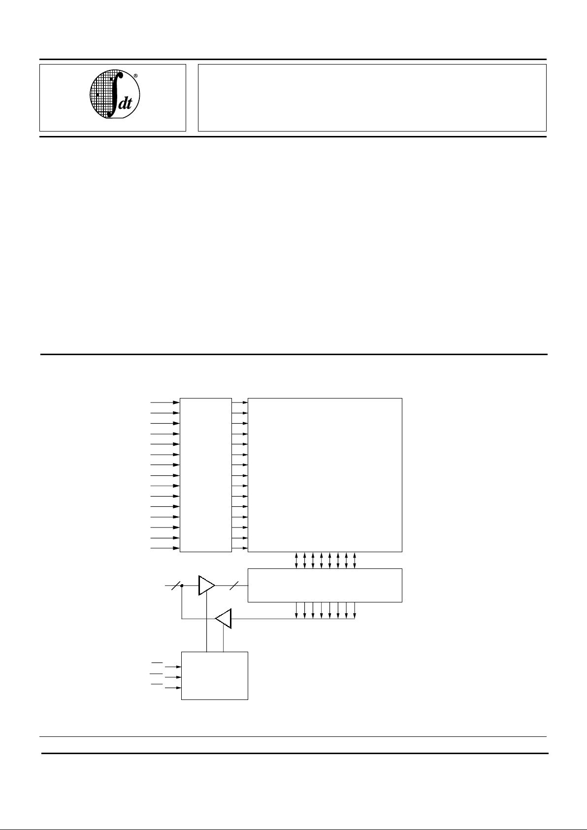
FUNCTIONAL BLOCK DIAGRAM
1
The IDT logo is a registered trademark of Integrated Device Technology, Inc.
A10
A11
A12
A13
A14
A0
A
1
A2
A
3
A4
A
5
A6
A
7
A8
A
9
262,144-BIT
MEMORY
ARRAY
I/O CONTROL
I/O0– I/O
7
CONTROL
LOGIC
WE
OE
CS
2948 drw 01
8 8
ADDRESS
DECODER
CMOS STATIC RAM
256K (32K x 8-BIT)
IDT71256SA
2
IDT71256SA
CMOS STATIC RAM 256K (32K x 8-BIT) INDUSTRIAL AND COMMERCIAL TEMPERATURE RANGES
ABSOLUTE MAXIMUM RATINGS
(1)
Symbol Rating Value Unit
V
CC Supply Voltage –0.5 to +7.0 V
Relative to GND
V
TERM Terminal Voltage –0.5 to VCC+0.5 V
Relative to GND
T
BIAS Temperature –55 to +125 °C
Under Bias
T
STG Storage –55 to +125 °C
Temperature
P
T Power 1.0 W
Dissipation
I
OUT DC Output 50 mA
Current
NOTES: 2948 tbl 02
1. Stresses greater than those listed under ABSOLUTE MAXIMUM
RATINGS may cause permanent damage to the device. This is a stress
rating only and functional operation of the device at these or any other
conditions above those indicated in the operational sections of this
specification is not implied. Exposure to absolute maximum rating
conditions for extended periods may affect reliability.
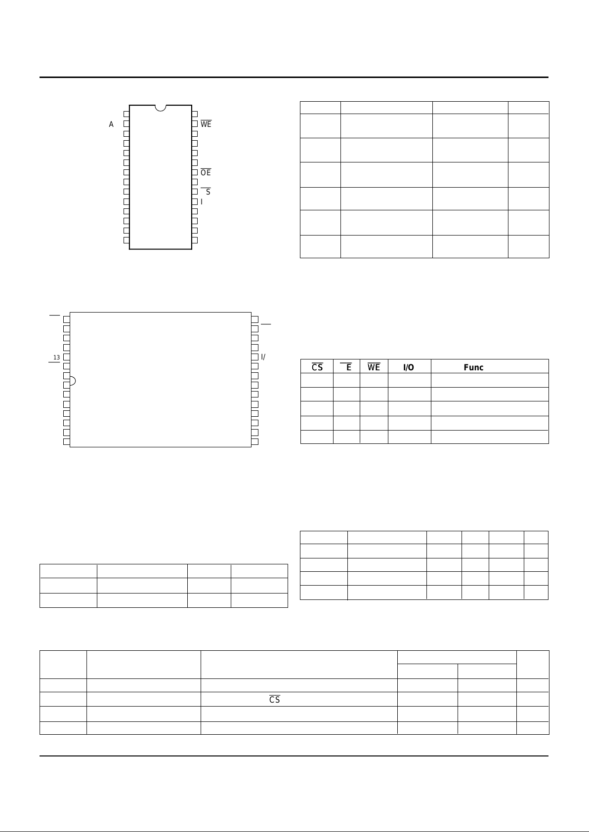
PIN CONFIGURATIONS
2948 tbl 05
DC ELECTRICAL CHARACTERISTICS
VCC = 5.0V ± 10%
IDT71256SA
Symbol Parameter Test Condition Min. Max. Unit
|I
LI| Input Leakage Current VCC = Max., VIN = GND to VCC — 5 µA
|I
LO| Output Leakage Current VCC = Max.,
CS
= VIH, VOUT = GND to VCC — 5 µA
V
OL Output Low Voltage IOL = 8mA, VCC = Min. — 0.4 V
V
OH Output High Voltage IOH = –4mA, VCC = Min. 2.4 — V
2948 drw 02
5
6
7
8
9
10
11
12
GND
1
2
3
4
24
23
22
21
20
19
18
17
SO28-5
P28-2
P28-1
13
14
28
27
26
25
A
7
A
6
A
5
A
4
A
3
A
2
A
1
A
0
I/O
0
I/O
1
I/O
2
V
CC
A
14
WE
A
13
A
8
A
10
A
11
OE
A
12
CS
I/O
7
I/O
6
I/O
5
I/O
4
I/O
3
A
9
16
15
DIP/SOJ
TOP VIEW
RECOMMENDED OPERATING
TEMPERATURE AND SUPPLY VOLTAGE
Grade Temperature GND VCC
Commercial 0°C to +70°C 0V 4.5V to 5.5V
Industrial -40°C to +85°C 0V 4.5V to 5.5V
3948 tbl 09
RECOMMENDED DC OPERATING
CONDITIONS
Symbol Parameter Min. Typ. Max. Unit
V
CC Supply Voltage 4.5 5.0 5.5 V
GND Supply Voltage 0 0 0 V
V
IH Input High Voltage 2.2 — VCC+0.5 V
V
IL Input Low Voltage –0.5
(1)
— 0.8 V
NOTE: 2948 tbl 01
1. VIL (min.) = –1.5V for pulse width less than 10ns, once per cycle.
TRUTH TABLE
(1,2)
CSCSOEOEWEWE I/O Function
L L H DATA
OUT Read Data
L X L DATA
IN Write Data
L H H High-Z Outputs Disabled
H X X High-Z Deselected — Standby (I
SB)
V
HC X X High-Z Deselected — Standby (ISB1)
NOTES: 2948 tbl 04
1. H = VIH, L = VIL, x = Don't care.
2. V
LC = 0.2V, VHC = VCC –0.2V.
3. Other inputs ≥V
HC or ≤VLC.
(3)
TSOP
TOP VIEW
2948 drw 11
22
23
24
25
26
27
28
1
2
3
4
5
7
6
21
20
19
18
17
16
15
14
13
12
11
10
9
8
A10
CS
I/O
7
I/O6
I/O5
I/O4
I/O3
GND
I/O
2
I/O1
I/O0
A0
A1
A2
SO28-8
OE
A
11
A9
A8
A13
A14
A7
A6
A5
A4
A3
A12
WE
V
CC