

Integrated Device Technology Inc IDT71024S15Y, IDT71024S15YI, IDT71024S17LB, IDT71024S17TY, IDT71024S17Y Datasheet
...
Integrated Device Technology, Inc.
CMOS STATIC RAM
1 MEG (128K x 8-BIT)
IDT71024
FEATURES:
• 128K x 8 advanced high-speed CMOS static RAM
• Commercial (0° to 70°C), Industrial (-40° to 85°C) and
Military (-55° to 125°C) temperature options
• Equal access and cycle times
— Military: 15/17/20/25ns
— Industrial: 15/20ns
— Commercial: 12/15/17/20ns
• Two Chip Selects plus one Output Enable pin
• Bidirectional inputs and outputs directly TTL-compatible
• Low power consumption via chip deselect
• Available in 300 and 400 mil Plastic SOJ, and LCC packages
• Military product compliant to MIL-STD-883, Class B
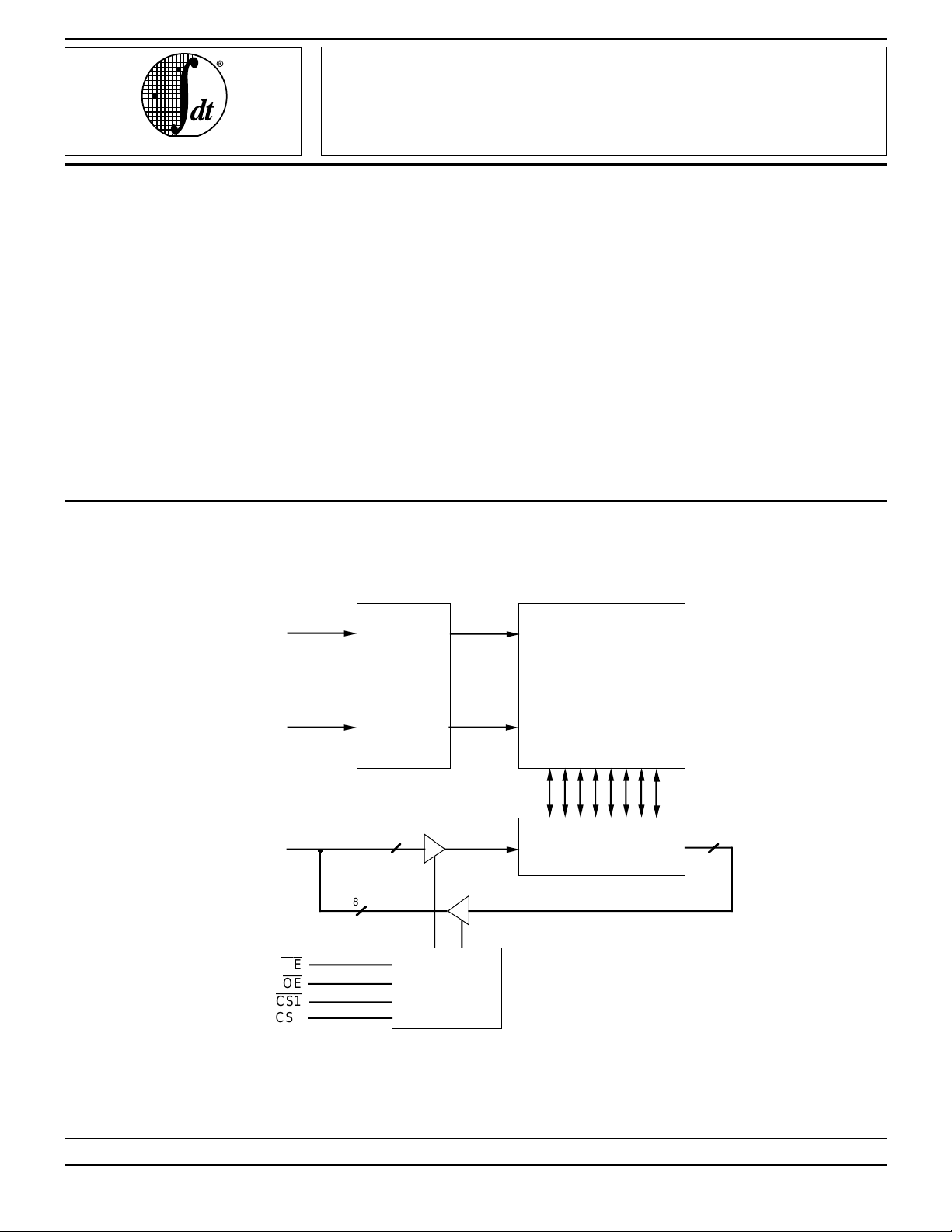
FUNCTIONAL BLOCK DIAGRAM
A
0
DESCRIPTION:
The IDT71024 is a 1,048,576-bit high-speed static RAM
organized as 128K x 8. It is fabricated using IDT’s highperformance, high-reliability CMOS technology. This stateof-the-art technology, combined with innovative circuit design
techniques, provides a cost-effective solution for high-speed
memory needs.
The IDT71024 has an output enable pin which operates as
fast as 6ns, with address access times as fast as 12ns
available. All bidirectional inputs and outputs of the IDT71024
are TTL-compatible and operation is from a single 5V supply.
Fully static asynchronous circuitry is used; no clocks or
refreshes are required for operation.
The IDT71024 is packaged in 32-pin 300 mil Plastic SOJ,
32-pin 400 mil Plastic SOJ, and 32-pin 400 x 820 mil LCC
packages.
A
I/O0 – I/O
16
7
WE
OE
CS1
CS2
•
•
•
•
ADDRESS
DECODER
8
8
CONTROL
LOGIC
•
•
1,048,576-BIT
MEMORY ARRAY
•
I/O CONTROL
8
2964 drw 01
The IDT logo is a registered trademark of Integrated Device Technology, Inc.
MILITARY, INDUSTRIAL AND COMMERCIAL TEMPERATURE RANGES MAY 1997
1996 Integrated Device Technology, Inc. DSC-2964/08
1
IDT71024
CMOS STATIC RAM 1MEG (128K x 8-BIT) MILITARY, INDUSTRIAL AND COMMERCIAL TEMPERATURE RANGES
PIN CONFIGURATION
1
NC
16
A7
A6
A5
A4
A3
A2
A1
A0
2
3
4
5
6
SO32-2
7
SO32-3
L32-2
8
9
10
11
12
13 20
14 19
15 18
A
A14
A12
I/O0
I/O1
I/O2
16GND 17
SOJ/LCC
TOP VIEW
TRUTH TABLE
(1,2)
INPUTS
WEWECS1
CS1
CS2
OE
OE
I/O FUNCTION
X H X X High-Z Deselected–Standby (I
(3)
HC
XV
X X High-Z Deselected–Standby (ISB1)
X X L X High-Z Deselected–Standby (I
(3)
LC
XXV
X High-Z Deselected–Standby (ISB1)
H L H H High-Z Outputs Disabled
H L H L DATA
L L H X DATA
NOTES: 2964 tbl 01
1. H = VIH, L = VIL, X = Don't care.
2. V
LC = 0.2V, VHC = VCC -0.2V.
3. Other inputs ≥V
HC or ≤VLC.
32
VCC
A15
31
CS2
30
WE
29
13
A
28
A8
27
A9
26
A11
25
OE
24
A10
23
CS1
22
I/O
21
I/O6
I/O5
I/O4
I/O3
2964 drw 02
OUT Read Data
IN Write Data
7
SB)
SB)
ABSOLUTE MAXIMUM RATINGS
(1)
Symbol Rating Com’l, Ind'l Mil. Unit
(2)
V
TERM
Terminal Voltage –0.5 to +7.0 –0.5 to +7.0 V
Relative to GND
T
BIAS Temperature –55 to +125 –65 to +135 °C
Under Bias
STG Storage –55 to +125 –65 to +150 °C
T
Temperature
P
T Power 1.25 1.25 W
Dissipation
I
OUT DC Output 50 50 mA
Current
NOTES: 2964 tbl 02
1. Stresses greater than those listed under ABSOLUTE MAXIMUM
RATINGS may cause permanent damage to the device. This is a stress
rating only and functional operation of the device at these or any other
conditions above those indicated in the operational sections of this
specification is not implied. Exposure to absolute maximum rating
conditions for extended periods may affect reliability.
2. V
TERM must not exceed VCC + 0.5V.
RECOMMENDED OPERATING
TEMPERATURE AND SUPPLY VOLTAGE
Grade Temperature GND VCC
Commercial 0°C to +70°C 0V 5.0V ± 0.5V
Industrial -40°C to +85°C 0V 5.0V ± 0.5V
Military -55°C to +125°C 0V 5.0V ± 0.5V
2964 tbl 03
RECOMMENDED DC OPERATING
CONDITIONS
Symbol Parameter Min. Typ. Max. Unit
CC Supply Voltage 4.5 5.0 5.5 V
V
GND Supply Voltage 0 0 0 V
IH Input High Voltage 2.2 — Vcc+0.5 V
V
IL Input Low Voltage –0.5
V
NOTE: 2964 tbl 04
1. VIL (min.) = –1.5V for pulse width less than 10ns, once per cycle.
(1)
— 0.8 V
DC ELECTRICAL CHARACTERISTICS
VCC = 5.0V ± 10%
IDT71024
Symbol Parameter Test Condition Min. Max. Unit
LI| Input Leakage Current VCC = Max., VIN = GND to VCC — 5 µA
|I
LO| Output Leakage Current VCC = Max.,
|I
OL Output LOW Voltage IOL = 8mA, VCC = Min. — 0.4 V
V
OH Output HIGH Voltage IOH = –4mA, VCC = Min. 2.4 — V
V
CS1
= VIH, CS2 = VIL, VOUT = GND to VCC — 5 µA
2964 tbl 05
2
IDT71024
CMOS STATIC RAM 1MEG (128K x 8-BIT) MILITARY, INDUSTRIAL AND COMMERCIAL TEMPERATURE RANGES
DC ELECTRICAL CHARACTERISTICS
(1)
(VCC = 5.0V ± 10%, VLC = 0.2V, VHC = VCC – 0.2V)
71024S12 71024S15 71024S17 71024S20 71024S25
Symbol Parameter Com'l. Mil. Com'l. Mil. Com'l. Mil. Com'l. Mil. Com'l. Mil. Unit
CC Dynamic Operating Current, CS2 ≥ VIH and 160 — 155 180 150 170 140 160 — 145 mA
I
CS2 ≥ V
V
IH and
CS1
CC = Max., f = fMAX
≤ VIL, Outputs Open,
(2)
ISB Standby Power Supply Current (TTL Level) 35 — 35 40 35 40 35 40 — 35 mA
CS1
V
IH or CS2 ≤ VIL, Outputs Open,
≥ V
CC = Max., f = fMAX
(2)
ISB1 Full Standby Power Supply Current 10 — 10 15 10 15 10 15 — 15 mA
(CMOS Level)
or CS2 ≤ VLC Outputs Open,
V
CC = Max., f = 0
NOTES: 2964 tbl 06
1. All values are maximum guaranteed values.
MAX = 1/tRC (all address inputs are cycling at fMAX); f = 0 means no address input lines are changing.
2. f
DC ELECTRICAL CHARACTERISTICS
CS1
≥ V
HC,
(2)
, VIN ≤ VLC or VIN ≥ VHC
(1)
(VCC = 5.0V ± 10%, VLC = 0.2V, VHC = VCC – 0.2V)
71024S15 71024S20
Symbol Parameter Industrial Industrial Unit
CC Dynamic Operating Current, CS2 ≥ VIH and 180 160 mA
I
CS2 ≥ V
V
ISB Standby Power Supply Current (TTL Level) 45 45 mA
CS1
V
ISB1 Full Standby Power Supply Current 15 15 mA
(CMOS Level)
or CS2 ≤ VLC Outputs Open,
V
NOTES: 2964 tbl 07
1. All values are maximum guaranteed values.
2. f
MAX = 1/tRC (all address inputs are cycling at fMAX); f = 0 means no address input lines are changing.
IH and
CS1
≤ VIL, Outputs Open,
CC = Max., f = fMAX
IH or CS2 ≤ VIL, Outputs Open,
≥ V
CC = Max., f = fMAX
CC = Max., f = 0
(2)
(2)
CS1
≥ V
(2)
, VIN ≤ VLC or VIN ≥ VHC
HC,
CAPACITANCE
(TA = +25°C, f = 1.0MHz, SOJ package)
Symbol Parameter
IN Input Capacitance VIN = 3dV 7 pF
C
I/O I/O Capacitance V OUT = 3dV 8 pF
C
NOTE: 2964 tbl 08
1. This parameter is guaranteed by device characterization, but is not production tested.
(1)
Conditions Max. Unit
3
 Loading...