

IDT IDT70V3599-89S User Manual
BE
查询IDT70V3589供应商
HIGH-SPEED 3.3V
128/64K x 36
SYNCHRONOUS
DUAL-PORT STATIC RAM
WITH 3.3V OR 2.5V INTERFACE
Features:
◆
True Dual-Port memory cells which allow simultaneous
access of the same memory location
◆
High-speed data access
– Commercial: 3.6ns (166MHz)/4.2ns (133MHz) (max.)
– Industrial: 4.2ns (133MHz) (max.)
◆
Selectable Pipelined or Flow-Through output mode
◆
Counter enable and repeat features
◆
Dual chip enables allow for depth expansion without
additional logic
◆
Full synchronous operation on both ports
– 6ns cycle time, 166MHz operation (12Gbps bandwidth)
– Fast 3.6ns clock to data out
– 1.7ns setup to clock and 0.5ns hold on all control, data, and
address inputs @ 166MHz
– Data input, address, byte enable and control registers
– Self-timed write allows fast cycle time
IDT70V3599/89S
◆
Separate byte controls for multiplexed bus and bus
matching compatibility
◆
Dual Cycle Deselect (DCD) for Pipelined Output mode
◆
LVTTL- compatible, 3.3V (±150mV) power supply
for core
◆
LVTTL compatible, selectable 3.3V (±150mV) or 2.5V
(±100mV) power supply for I/Os and control signals on
each port
◆
Industrial temperature range (-40°C to +85°C) is
available at 133MHz.
◆
Available in a 208-pin Plastic Quad Flatpack (PQFP),
208-pin fine pitch Ball Grid Array (fpBGA), and 256-pin Ball
Grid Array (BGA)
◆
Supports JTAG features compliant with IEEE 1149.1
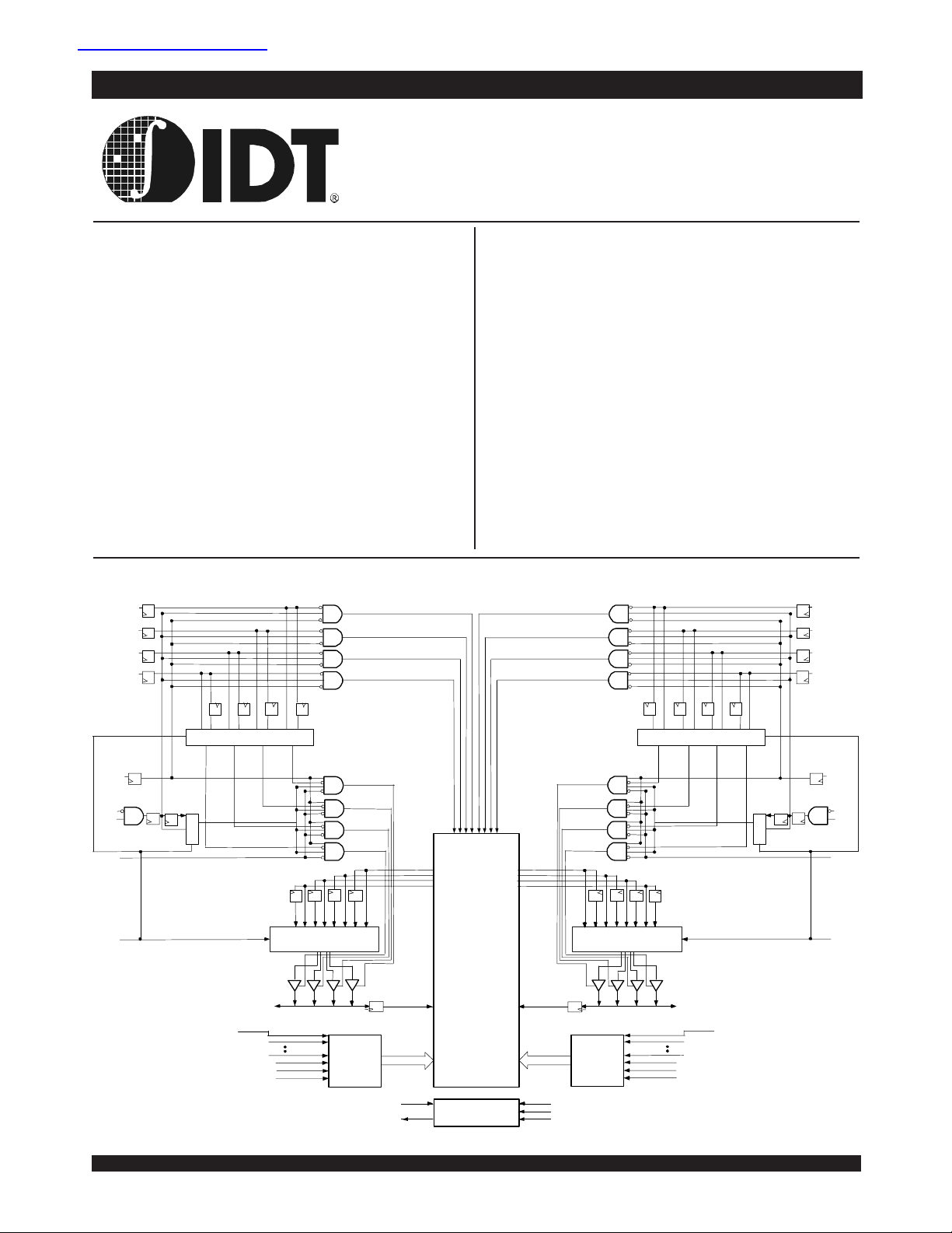
Functional Block Diagram
BE
3L
BE
2L
BE
1L
BE
0L
FT/PIPE
CE
CE
FT/PIPE
R/W
OE
L
L
0L
1L
L
L
1/0
abcd
1
0
1/0
I/O0L-I/O
CLK
L
REPEAT
NOTE:
16 is a NC for IDT70V3589.
1. A
©2003 Integrated Device Technology, Inc.
A
CNTEN
ADS
0d 1d0c 1c0b 1b0a 1a
1d 0d 1c 0c
abcd
1b 0b 1a 0a
Counter/
Address
Reg.
0/1
35L
(1)
16L
A
0L
L
L
L
TDO
3R
BE
2R
BE
1R
BE
0R
1a 0a1b 0b1c 0c1d 0d
dcba
B
B
B
B
B
B
B
B
W
W
W
W
W
W
W
W
0
1
2
3
2
3
1
0
L
L
L
L
R
R
R
R
Dout0-8_L
Dout9-17_L
Dout18- 26_L
Dout27- 35_L
Din_L
ADDR_L
TDI
Dout18 -26_R
Dout27 -35_R
128Kx 36
MEMORY
ARRAY
JTAG
Dout0-8_R
Dout9-17_R
Din_R
ADDR_R
TCK
TMS
TRST
0b 1b0a 1a
Counter/
Address
Reg.
dcba
0d 1d0c 1c
0/1
I/O0R- I/O
35R
(1)
A
16R
A
0R
REPEAT
R
ADS
R
CNTEN
R
1/0
1
0
1/0
CLK
,
R
5617 tbl 01
FT/PIPE
R/W
CE
CE
OE
FT/PIPE
R
R
0R
1R
R
R
MAY 2003
1
DSC 5617/6
IDT70V3599/89S
High-Speed 3.3V 128/64K x 36 Dual-Port Synchronous Static RAM Industrial and Commercial Temperature Ranges
Description:
The IDT70V3599/89 is a high-speed 128/64K x 36 bit synchronous
Dual-Port RAM. The memory array utilizes Dual-Port memory cells to
allow simultaneous access of any address from both ports. Registers on
control, data, and address inputs provide minimal setup and hold
times. The timing latitude provided by this approach allows systems
to be designed with very short cycle times. With an input data register, the
IDT70V3599/89 has been optimized for applications having unidirectional
or bidirectional data flow in bursts. An automatic power down feature,
controlled by CE
0 and CE1, permits the on-chip circuitry of each port to
enter a very low standby power mode.
The 70V3599/89 can support an operating voltage of either 3.3V or
2.5V on one or both ports, controllable by the OPT pins. The power supply
for the core of the device (V
DD) remains at 3.3V.
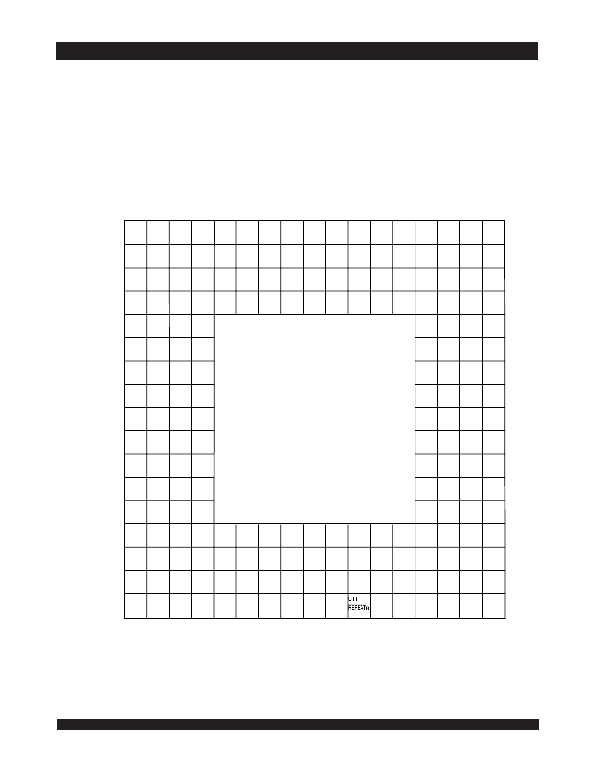
A2
B2
C2
I/O
D2
E2
I/O
F2
I/O
G2
H2
I/O
J2
K2
L2
M2
N2
P2
R2
I/O
T2
U2
I/O
IO
I/O
I/O
I/O
I/O
18L
V
SS
19R
V
SS
22R
23R
V
SS
26R
V
DD
V
SS
V
SS
32L
33L
35L
(1,2,3,4,5)
A3
V
SS
B3
I/O
18R
C3
V
DDQR
D3
I/O
21L
E3
V
DDQR
F3
I/O
24L
G3
I/O
H3
V
DDQR
J3
V
SS
K3
I/O
27R
L3
V
DDQR
28L
M3
29L
I/O
30R
N3
I/O
31R
P3
V
DDQR
R3
I/O
34R
T3
34L
V
DDQL
U3
PL/
FT
25L
A8
A7
A
8L
A
12L
B7
B8
A
9L
BE
2L
C8
C7
BE
10L
3L
D8
BE
0L
7L
A
D7
A
70V3599/89BF
BF-208
208-Pin fpBGA
Top View
P8
P7
A
8R
A
12R
R7
R8
BE
A
T7
A
U7
2R
9R
T8
BE
3R
10R
U8
A
7R
BE
0R
A9
A10
BE
1L
V
DD
B9
B10
CE
0L
V
SS
C10
C9
V
SS
CE
1L
D9
D10
V
DD
OE
L
(6)
(7)
P9
P10
BE
1R
V
DD
R10
R9
CE
0R
V
SS
T9
T10
CE
1R
V
SS
U10
U9
OE
V
R
DD
L
A5
NC
B5
NC
C5
NC
D5
A
15L
P5
TRST
R5
NC
T5
NC
U5
A
15R
A6
(1)
A
16L
B6
A
13L
C6
A
14L
D6
A
11L
P6
(1)
A
16R
R6
A
13R
T6
A
14R
U6
A
11R
A4
TDO
B4
TDI
C4
PL/
FT
D4
I/O
20L
E4
I/O
21R
F4
V
SS
G4
I/O
24R
H4
I/O
25R
J4
V
SS
K4
V
SS
L4
I/O
27L
M4
V
SS
N4
I/O
30L
P4
I/O
35R
R4
TCK
T4
TMS
U4
R
NC
A11
CLK
B11
ADS
C11
R/W
D11
REPEAT
P11
CLK
R11
ADS
T11
R/W
L
L
L
L
R
R
R
A12
CNTEN
B12
A
5L
C12
A
6L
D12
A
3L
P12
CNTEN
R12
A
5R
T12
A
6R
U12
A
3R
A14
A13
A
L
B13
C13
D13
P13
R
R13
T13
U13
0L
A
4L
B14
A
1L
V
SS
C14
A
2L
V
DD
D14
I/O
17R
V
DD
E14
I/O
12L
F14
V
SS
G14
I/O
9L
H14
V
DD
J14
V
SS
K14
I/O
7R
L14
I/O
6R
M14
V
SS
N14
I/O
3R
P14
I/O
A
A
A
A
2L
4R
R14
1R
V
SS
T14
2R
V
SS
U14
0R
V
DD
Pin Configuration
06/28/0 2
A1
IO
19L
B1
I/O
20R
C1
V
DDQL
D1
I/O
22L
E1
I/O
23L
F1
V
DDQL
G1
I/O
26L
H1
V
DD
J1
V
DDQL
K1
I/O
28R
L1
I/O
29R
M1
V
DDQL
N1
I/O
31L
P1
I/O
32R
R1
V
SS
T1
I/O
33R
U1
V
SS
NOTES:
1. A
16 is a NC for IDT70V3589.
DD pins must be connected to 3.3V power supply.
2. All V
DDQ pins must be connected to appropriate power supply: 3.3V if OPT pin for that port is set to VIH (3.3V), and 2.5V if OPT pin for that port is
3. All V
4. All V
IL (0V).
set to V
SS pins must be connected to ground supply.
5. Package body is approximately 15mm x 15mm x 1.4mm with 0.8mm ball pitch.
6. This package code is used to reference the package diagram.
7. This text does not indicate orientation of the actual part-marking.
6.42
2
A15
OPT
B15
V
DDQR
C15
I/O
D15
V
E15
I/O
F15
I/O
G15
V
DDQL
H15
IO
J15
V
K15
V
L15
I/O
M15
I/O
N15
V
P15
I/O
R15
V
T15
I/O
U15
OPT
16R
DDQL
13R
12R
9R
DD
DDQL
7L
6L
DDQL
3L
DDQL
0R
L
R
A16
I/O
B16
I/O
C16
I/O
D16
I/O
E16
F16
I/O
G16
I/O
H16
J16
K16
I/O
L16
M16
N16
I/O
P16
R16
T16
U16
I/O
I/O
I/O
17L
16L
15L
14L
V
SS
11L
10L
V
SS
V
SS
V
SS
4R
V
SS
V
SS
A17
V
SS
B17
I/O
15R
C17
V
SS
D17
I/O
14R
E17
I/O
13L
F17
V
DDQR
G17
I/O
11R
H17
I/O
10R
J17
V
DDQR
K17
8R
V
SS
L17
I/O
8L
M17
V
DDQR
5R
N17
I/O
P17
I/O
4L
R17
1R
V
DDQR
T17
I/O
2R
U17
I/O
1L
0L
5617 drw 02c
5L
,

IDT70V3599/89S
High-Speed 3.3V 128/64K x 36 Dual-Port Synchronous Static RAM Industrial and Commercial Temperature Ranges
Pin Configuration
(1,2,3,4,5)
(con't.)
06/2 8/02
A1
NC
B1
I/O
18L
C1
I/O
18R
D1
I/O
20R
E1
I/O
21R
F1
I/O
23L
G1
I/O
24R
H1
I/O
26L
J1
I/O
27L
K1
I/O
29R
L1
I/O
30L
M1
I/O
32R
N1
I/O
33L
P1
I/O
35R
R1
I/O
35L
T1
NC
A3
A2
NC
TDI
B3
B2
TDO
NC
C2
C3
V
19L
19R
21L
22R
24L
25R
28R
29L
31R
32L
34R
34L
SS
D3
I/O
20L
E3
I/O
22L
F3
I/O
23R
G3
I/O
25L
H3
I/O
26R
J3
I/O
27R
K3
I/O
28L
L3
I/O
30R
M3
I/O
31L
N3
I/O
33R
P3
TMSP4A
I/O
D2
I/O
E2
I/O
F2
I/O
G2
I/O
H2
I/O
J2
I/O
K2
I/O
L2
I/O
M2
I/O
N2
I/O
P2
I/O
R2
NCR3TRSTR4NC
T2
TCKT3NC
A4
NC
B4
NC
C4
A
16L
D4
PIPE/
E4
V
DDQL
F4
V
DDQL
G4
V
DDQR
H4
V
DDQR
J4
V
DDQL
K4
V
DDQL
L4
V
DDQR
M4
V
DDQR
N4
PIPE/
16R
T4
NC
FT
FT
70V3599/89BC
BC-256
(6)
256-Pin BGA
2L
3L
DDQR
V
SS
SS
SS
SS
SS
V
SS
V
SS
V
SS
DDQL
1R
3R
2R
(7)
A12
B12
C12
D12
V
E12
F12
G12
H12
J12
K12
L12
M12
N12
V
P12
R12
T12
A
A
A
DDQR
V
V
DD
V
SS
V
SS
V
SS
V
SS
V
DD
V
DD
DDQL
A
A
A
DD
6R
4R
A13
A14
A
2L
A
1L
A
3L
DD
DDQL
DDQR
DDQL
DDQL
DD
3R
1R
2R
B14
V
C14
OPT
D14
I/O
E14
I/O
F14
I/O
G14
I/O
H14
I/O
J14
I/O
K14
I/O
L14
I/O
M14
I/O
N14
I/O
P14
I/O
R14
OPT
T14
A
0L
DD
L
15R
13L
12R
10L
9R
8R
6R
5L
3R
2L
0L
R
0R
5L
A
B13
4L
C13
6L
D13
V
E13
V
DDQR
F13
V
DDQR
G13
V
H13
V
DDQL
J13
V
DDQR
K13
V
L13
V
M13
V
N13
V
P13
A
R13
A
T13
5R
A
A16
A15
NC
B15
B16
I/O
17L
C16
C15
I/O
17R
D15
D16
I/O
15L
E16
E15
I/O
14L
F15
F16
I/O
13R
G15
G16
I/O
I/O
11L
H16
H15
I/O
IO
9L
J15
J16
I/O
7R
K15
K16
I/O
6L
L15
L16
I/O
4R
M16
M15
I/O
3L
N16
N15
I/O
1R
P15
P16
I/O
0R
R16
R15
NC
T15NCT16
I/O
I/O
I/O
I/O
I/O
I/O
I/O
I/O
I/O
I/O
NC
NC
NC
NC
16L
16R
14R
12L
11R
10R
8L
7L
5R
4L
2R
1L
,
A10
OE
B10
R/W
C10
CLK
D10
V
DDQL
E10
V
F10
V
G10
V
H10
V
J10
V
K10
V
L10
V
M10
V
N10
V
DDQR
P10
CLK
R10
R/W
T10
OE
A11
CNTEN
L
L
B11
REPEA T
L
L
C11
ADS
L
L
D11
V
DDQR
E11
SS
V
DD
F11
SS
V
SS
G11
SS
V
SS
H11
V
SS
SS
J11
SS
V
SS
K11
SS
V
SS
L11
V
SS
SS
M11
SS
V
DD
N11
V
DDQL
P11
R
ADS
R
R11
REPEAT
R
R
T11
CNTEN
R
R
A9
CE
1L
B9
CE
0L
C9
1L
BE
0L
D9
V
DDQL
E9
V
SS
F9
V
SS
G9
V
SS
H9
V
SS
J9
V
SS
K9
V
SS
L9
V
SS
M9
V
SS
N9
V
DDQR
P9
BE
0R
R9
CE
0R
T9
CE
1R
Top View
A7
B7
C7
D7
V
E7
F7
G7
H7
J7
K7
L7
M7
N7
V
P7
R7
T7
A
8L
A
9L
A
7L
DDQR
V
SS
V
SS
V
SS
V
SS
V
SS
V
SS
V
SS
V
SS
DDQL
A
7R
A
9R
A
8R
A8
BE
B8
BE
C8
BE
D8
V
E8
F8
V
G8
V
H8
V
J8
V
K8
L8
M8
N8
V
P8
BE
R8
BE
T8
BE
A6
A5
A
11L
A
14L
B6
B5
A
12L
A
15L
C6
C5
(1)
L
R
(1)
D5
V
E5
F5
G5
H5
J5
K5
L5
M5
N5
V
P5
R5
T5
A
DDQL
V
V
V
V
V
V
V
V
DDQR
A
13R
A
A
13L
DD
DD
SS
SS
SS
SS
DD
DD
15R
14R
D6
V
E6
F6
G6
H6
J6
K6
L6
M6
N6
V
P6
R6
T6
A
10L
DDQL
V
V
V
V
V
V
V
V
DDQR
A
10R
A
12R
A
11R
DD
SS
SS
SS
SS
SS
SS
DD
NOTES:
1. A
16 is a NC for IDT70V3589.
DD pins must be connected to 3.3V power supply.
2. All V
DDQ pins must be connected to appropriate power supply: 3.3V if OPT pin for that port is set to VIH (3.3V), and 2.5V if OPT pin for that port is
3. All V
4. All V
IL (0V).
set to V
SS pins must be connected to ground supply.
5. Package body is approximately 17mm x 17mm x 1.4mm, with 1.0mm ball-pitch.
6. This package code is used to reference the package diagram.
7. This text does not indicate orientation of the actual part-marking.
6.42
3
5617 drw 02d
,

IDT70V3599/89S
High-Speed 3.3V 128/64K x 36 Dual-Port Synchronous Static RAM Industrial and Commercial Temperature Ranges
R
R
Q
8
1
D
D
O
/
V
I
6
7
0
0
2
2
5
4
5
5
L
R
5
Q
3
D
O
D
/
I
V
(1,2,3,4,5)
L
L
T
8
F
I
1
/
S
S
L
D
O
/
I
V
P
T
4
5
2
3
0
0
0
0
2
2
2
2
9
8
7
6
5
5
5
5
L
R
K
S
5
T
3
C
M
F
T
/
O
T
/
L
I
P
(con't.)
)
1
(
L
L
L
L
L
L
O
6
5
C
C
C
1
D
T
1
0
2
1
A
A
N
N
N
6
7
8
9
0
9
9
9
9
0
2
1
1
1
1
L
4
3
2
1
0
L
L
1
1
1
A
A
A
5
3
4
9
9
9
1
1
1
L
1
1
9
8
7
A
A
A
A
A
0
1
2
8
9
9
9
9
8
8
1
1
1
1
1
L
L
3
E
B
7
8
1
L
L
L
L
1
0
2
1
0
E
E
E
E
E
B
B
B
C
C
2
3
4
5
6
8
8
8
8
8
1
1
1
1
1
70V3599/89DR
DR-208
208-Pin PQFP
Top View
9
8
7
6
5
4
3
2
1
0
9
8
7
6
5
4
3
2
1
0
6
6
6
6
6
)
T
1
C
C
C
(
S
R
N
N
N
6
R
1
T
A
6
6
6
6
6
R
R
R
R
R
5
4
3
2
1
1
1
1
1
1
A
A
A
A
A
7
7
7
7
7
R
R
R
R
R
0
9
8
7
3
1
E
A
A
A
A
B
7
7
7
7
7
R
R
R
R
R
2
1
0
1
0
E
E
E
E
E
B
B
B
C
C
L
K
D
D
S
S
L
D
D
S
S
V
V
V
V
C
9
0
1
7
8
7
8
8
7
7
1
1
1
1
1
(6)
(7)
4
3
2
1
0
8
8
8
8
8
S
S
D
D
R
S
S
D
D
K
V
V
V
V
L
C
L
L
T
A
N
L
E
E
L
L
T
P
S
L
L
W
E
/
D
O
R
A
6
4
5
7
7
7
1
1
1
7
6
5
8
8
8
R
R
R
E
S
W
/
D
O
R
A
L
N
E
6
5
4
C
R
A
A
A
3
1
2
0
9
7
7
7
7
6
1
1
1
1
1
2
1
0
9
8
9
9
9
8
8
R
R
R
R
R
6
5
4
T
N
A
A
A
A
E
E
T
P
N
E
C
R
D
L
3
A
8
6
1
3
9
R
3
A
D
L
L
L
2
1
0
D
D
A
A
A
V
V
3
4
5
6
7
6
6
6
6
6
1
1
1
1
1
8
7
6
5
4
9
9
9
9
9
S
D
R
R
R
2
1
0
S
D
A
A
A
V
V
R
L
R
L
Q
7
7
T
1
1
D
S
S
V
2
6
1
9
9
S
S
V
S
P
D
S
O
O
/
/
O
I
I
V
V
9
0
1
7
8
5
6
6
5
5
1
1
1
1
1
I/O
16L
156
I/O
16R
155
I/O
15L
154
I/O
15R
153
V
SS
152
V
DDQL
151
I/O
14L
150
I/O
14R
149
I/O
13L
148
I/O
13R
147
V
SS
146
V
DDQR
145
I/O
12L
144
I/O
12R
143
I/O
11L
142
I/O
11R
141
V
SS
140
V
DDQL
139
I/O
10L
138
I/O
10R
137
I/O
9L
136
I/O
9R
135
V
SS
134
V
DDQR
133
V
DD
132
V
DD
131
V
SS
130
V
SS
129
V
SS
128
V
DDQL
127
I/O
8R
126
I/O
8L
125
I/O
7R
124
I/O
7L
123
V
SS
122
V
DDQR
121
I/O
6R
120
I/O
6L
119
I/O
5R
118
I/O
5L
117
V
SS
116
V
DDQL
115
I/O
4R
114
I/O
4L
113
I/O
3R
112
I/O
3L
111
V
SS
110
V
DDQR
109
I/O
2R
108
I/O
2L
107
I/O
1R
106
I/O
1L
105
4
3
2
1
0
0
0
0
0
0
1
1
1
1
1
L
R
0
T
O
P
/
I
O
5617 drw 02a
L
S
R
0
Q
S
D
V
O
/
D
I
V
,
Pin Configuration
S
S
06/2 8/02
V
8
0
2
1
I/O
19L
2
I/O
19R
3
I/O
20L
4
I/O
20R
5
V
DDQL
6
V
SS
7
I/O
21L
8
I/O
21R
9
I/O
22L
10
I/O
22R
I/O
I/O
I/O
I/O
V
I/O
I/O
I/O
I/O
V
I/O
I/O
I/O
I/O
I/O
I/O
I/O
I/O
V
I/O
I/O
I/O
I/O
I/O
I/O
I/O
I/O
DDQR
V
DDQL
V
DDQR
V
V
V
V
V
DDQL
V
DDQR
V
DDQL
V
DDQR
V
11
12
SS
13
23L
14
23R
15
24L
24R
16
17
18
SS
25L
19
25R
20
26L
21
26R
22
23
SS
24
DD
25
DD
26
SS
27
SS
28
29
SS
30
27R
31
27L
32
28R
33
28L
34
35
SS
36
29R
37
29L
38
30R
39
30L
40
41
SS
42
43
31R
44
31L
32R
45
46
32L
47
48
SS
49
33R
50
33L
51
34R
52
34L
3
5
S
S
V
V
V
V
V
NOTES:
1. A16 is a NC for IDT70V3589.
2. All VDD pins must be connected to 3.3V power supply.
DDQ pins must be connected to appropriate power supply: 3.3V if OPT pin for that port is set to VIH (3.3V), and 2.5V if OPT pin for that port is set to VIL (0V).
3. All V
SS pins must be connected to ground supply.
4. All V
5. Package body is approximately 28mm x 28mm x 3.5mm.
6. This package code is used to reference the package diagram.
7. This text does not indicate orientation of the actual part-marking.
6.42
4
IDT70V3599/89S
High-Speed 3.3V 128/64K x 36 Dual-Port Synchronous Static RAM Industrial and Commercial Temperature Ranges
Pin Names
Left Port Right Port Names
0L
,
CE
CE
R/W
L
L
OE
0L
- A
16 L
A
0L
- I/O
I/O
L
CLK
L
PL/FT
L
ADS
CNTEN
L
REPEAT
BE0L - BE
V
OPT
1L
(1)
35L
L
3L
DD Q L
CE
0R
,
CE
1R
R/ W
R
OE
R
A0R - A
I/O0R - I/O
CLK
PL/FT
ADS
CNTEN
REPEAT
BE0R - BE
L
V
DD
V
SS
(1 )
16R
35R
R
R
R
R
R
3R
V
DDQR
OPT
R
TDI Test Data Inp ut
TDO Test Data Output
TCK Test Logic Clock (10MHz)
TMS Test Mode Select
TRST
Chip Enables
Read/ Write Enable
Output Enable
Address
Data Input/Outp ut
Clock
Pipeline/Flow-Through
Address Strobe Enable
Counter Enable
Counter Repeat
Byte Enables (9-bit bytes)
Po wer (I/O Bus) (3.3V o r 2.5V)
Op tio n for selecti ng V
Po wer (3.3V)
Ground (0V)
Re se t (Initialize TAP Co ntrol le r)
(5)
(4)
(5)
(2)
NOTES:
(2,3)
DDQX
(2 )
16 is a NC for IDT70V3589.
1. A
2. V
DD, OPTX, and VDDQX must be set to appropriate operating levels prior to
applying inputs on the I/Os and controls for that port.
X selects the operating voltage levels for the I/Os and controls on that port.
3. OPT
X is set to VIH (3.3V), then that port's I/Os and controls will operate at 3.3V
If OPT
levels and V
DDQX must be supplied at 3.3V. If OPTX is set to VIL (0V), then that
port's I/Os and address controls will operate at 2.5V levels and V
DDQX must be
supplied at 2.5V. The OPT pins are independent of one another—both ports can
operate at 3.3V levels, both can operate at 2.5V levels, or either can operate
at 3.3V with the other at 2.5V.
X is asserted, the counter will reset to the last valid address loaded
X.
IH, i.e., the
56 17 tbl 01
4. When REPEAT
via ADS
5. Chip Enables and Byte Enables are double buffered when PL/FT = V
signals take two cycles to deselect.
6.42
5
IDT70V3599/89S
High-Speed 3.3V 128/64K x 36 Dual-Port Synchronous Static RAM Industrial and Commercial Temperature Ranges
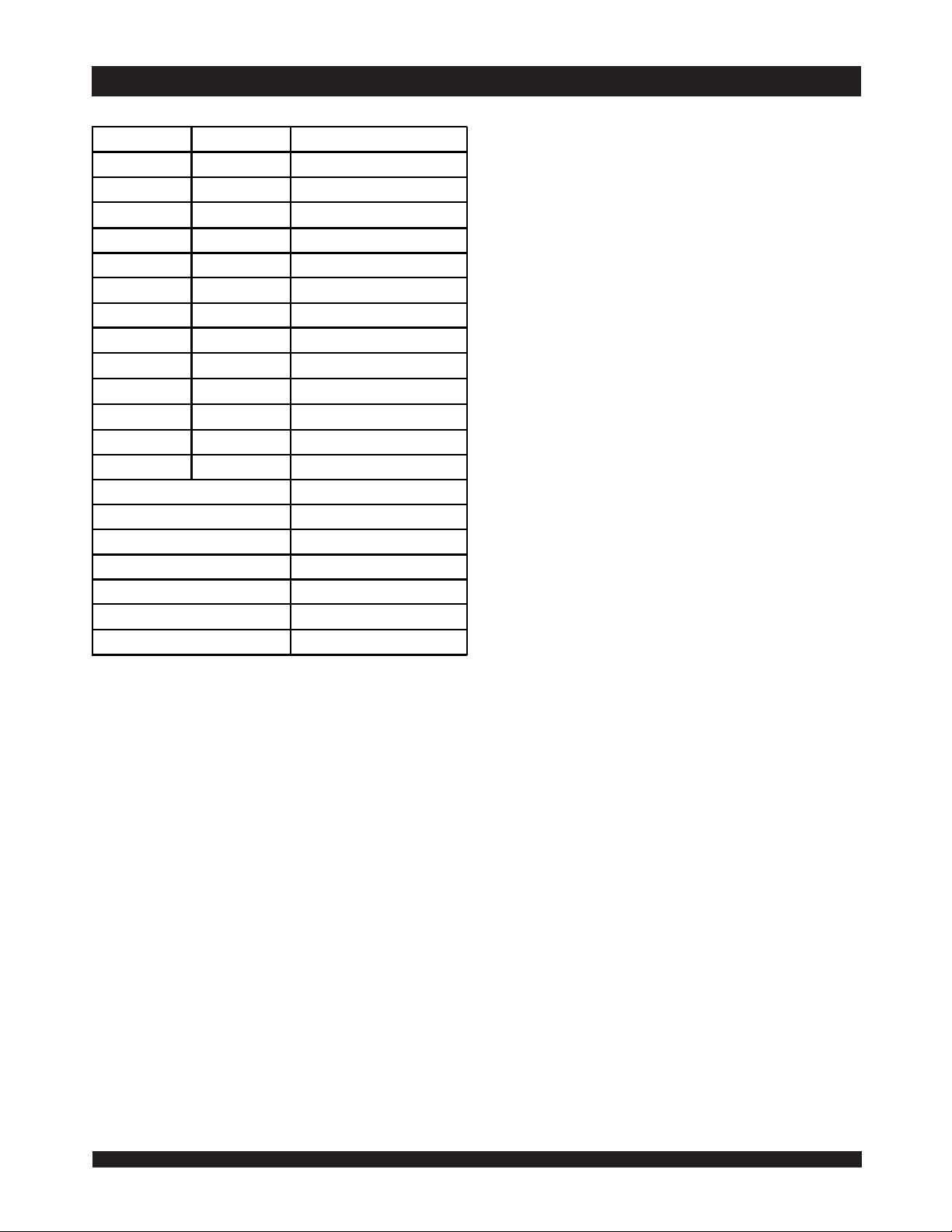
Truth Table I—Read/Write and Enable Control
CE
OE
CLK
CE
X
↑
X
↑
X
↑
X
↑
X
↑
X
↑
X
↑
X
↑
X
↑
X
↑
L
↑
L
↑
L
↑
L
↑
L
↑
L
↑
L
↑
H
↑
1
0
HXXXXXXHigh-ZHigh-ZHigh-ZHigh-ZDeselected–Power Down
XLXXXXXHigh-ZHigh-ZHigh-ZHigh-ZDeselected–Power Down
L H H H H H X High-Z High-Z High-Z High-Z All Bytes Deselected
L H H H H L L High-Z High-Z High-Z D
LHHHLHLHigh-ZHigh-Z D
LHHLHHLHigh-Z D
LHLHHHL D
L H H H L L L Hig h-Z Hig h-Z D
LHLLHHL D
LHLLLLL D
L H H H H L H High-Z High-Z High-Z D
LHHHLHHHigh-ZHigh-Z D
LHHLHHHHigh-ZD
LHLHHHH D
LHHHLLHHigh-ZHigh-ZD
LHLLHHH D
LHLLLLH D
LHLLLLXHigh-ZHigh-ZHigh-ZHigh-ZOutputs Disabled
NOTES:
1. "H" = V
IH, "L" = VIL, "X" = Don't Care.
2. ADS, CNTEN, REPEAT = V
BE3BE2BE1BE
IH.
Byte 3
R/W
0
I/O
OUT
OUT
OUT
Byte 2
I/O
27-35
IN
IN
IN
18-26
IN
High-Z High-Z High-Z Write to Byte 3 Only
D
IN
D
IN
OUT
High-Z High-Z High-Z Read Byte 3 Only
D
OUT
D
OUT
(1,2,3,4)
Byte 1
I/O
Byte 0
I/O
9-17
IN
0-8
IN
High-Z Write to Byte 1 Only
MODE
Write to Byte 0 Only
High-Z High-Z Write to Byte 2 Only
IN
D
IN
Write to Lower 2 Bytes Only
High-Z High-Z Write to Upper 2 bytes Only
D
IN
OUT
D
IN
Write to All By tes
OUT
Rea d B yte 0 Only
Hig h-Z Rea d B yte 1 Only
High-Z High-Z Read Byte 2 Only
OUT
D
OUT
Rea d Lowe r 2 B yte s Only
High-Z High-Z Read Upper 2 Bytes Only
D
OUT
D
OUT
Read All Bytes
5617 tb l 02
3. OE is an asynchronous input signal.
4. It is possible to read or write any combination of bytes during a given access. A few representative samples have been illustrated here.
Truth Table II—Address Counter Control
External
Addr ess
Internal
Addr ess
XXAn
An X An
An Ap Ap
XApAp + 1↑H L
NOTES:
Previ ous
1. "H" = V
IH, "L" = VIL, "X" = Don't Care.
2. Read and write operations are controlled by the appropriate setting of R/W, CE
Internal
Addr ess
Used CLK
ADS CNTEN REPEAT
XX L
↑
(4)
L
↑
↑
XHD
HH H D
(5)
(6)
(4)
HD
(1,2)
(3)
I/O
D
I/O
(0) Counter Reset to last valid ADS load
I/O
(n) External Address Used
I/O
(p) External Address Blocked—Counter disabled (Ap reused)
I/ O
(p+1) Counter Enabled—Internal Address generation
0, CE1, BEn and OE.
MODE
5617 tb l 03
3. Outputs configured in flow-through output mode: if outputs are in pipelined mode the date out will be delayed by one cycle.
4. ADS and REPEAT are independent of all other memory control signals including CE
5. The address counter advances if CNTEN = V
IL on the rising edge of CLK, regardless of all other memory control signals including CE0, CE1, BEn.
0, CE1 and BEn
6. When REPEAT is asserted, the counter will reset to the last valid address loaded via ADS. This value is not set at power-up: a known location should be loaded
via ADS during initialization if desired. Any subsequent ADS access during operations will update the REPEAT address location.
6.42
6
IDT70V3599/89S
High-Speed 3.3V 128/64K x 36 Dual-Port Synchronous Static RAM Industrial and Commercial Temperature Ranges
Recommended Operating
DD
Unit
o
o
o
(1)
5617 tbl 04
C
C
C
5617 tbl 06
Temperature and Supply Voltage
Ambient
Grade
Commercial 0OC to +70OC0V3.3V + 150mV
Industrial -40
NOTES:
1. This is the parameter TA. This is the "instant on" case temperature.
Absolute Maximum Ratings
Symbol Rating Comm ercial
(2 )
TERM
V
(3)
BIAS
T
STG
T
T
JN
I
OUT
NOTES:
1. Stresses greater than those listed under ABSOLUTE MAXIMUM RATINGS may
cause permanent damage to the device. This is a stress rating only and functional
operation of the device at these or any other conditions above those indicated
in the operational sections of this specification is not implied. Exposure to absolute
maximum rating conditions for extended periods may affect reliability.
TERM must not exceed VDD + 150mV for more than 25% of the cycle time or
2. V
4ns maximum, and is limited to
3. Ambient Temperature Under Bias. No AC Conditions. Chip Deselected.
Terminal Voltage
with Resp ect to GND
Temperature Under Bias -55 to +125
Sto rag e Tempe rature -65 to +150
Junction Temperature +150
DC Outp ut Current 50 mA
Temperature GND V
O
C to +85OC0V3.3V + 150mV
(1)
& Industrial
-0.5 to +4.6 V
< 20mA for the period of VTERM > VDD + 150mV.
Recommended DC Operating
Conditions with V
Symbol Parameter Min. Typ. Max. Unit
DD
Core Sup ply Voltage 3.15 3.3 3.45 V
V
DDQ
I/O S upply Voltage
V
SS
Ground 0 0 0 V
V
Input Hig h Vo lta ge
IH
V
(Ad dre ss & Co ntrol Inp uts)
V
IH
Input High Voltage - I/O
IL
Input Lo w Voltag e -0. 3
V
NOTES:
1. Undershoot of V
TERM must not exceed VDDQ + 100mV.
2. V
3. To select operation at 2.5V levels on the I/Os and controls of a given port, the
OPT pin for that port must be set to V
as indicated above.
IL > -1.5V for pulse width less than 10ns is allowed.
DDQ at 2.5V
(3 )
2.4 2.5 2.6 V
____
V
DDQ
V
DDQ
+ 100mV
+ 100mV
0.7 V
1.7
(3)
IL (0V), and VDDQX for that port must be supplied
1.7
____
(1)
____
(2 )
(2 )
5617 tb l 05a
V
V
Recommended DC Operating
Conditions with V
Symbol Parameter Min. Typ. Max. Unit
DD
Core Supply Voltage 3.15 3.3 3.45 V
V
V
DDQ
I/O Supply Voltage
SS
Ground 0 0 0 V
V
Inp ut Hig h Vo ltage
IH
V
(Address & Control Inputs)
IH
Inp ut Hig h Vo ltage - I/O
V
V
IL
Input Lo w Voltage -0.3
NOTES:
1. Undershoot of V
TERM must not exceed VDDQ + 150mV.
2. V
3. To select operation at 3.3V levels on the I/Os and controls of a given port, the
OPT pin for that port must be set to V
supplied as indicated above.
IL > -1.5V for pulse width less than 10ns is allowed.
DDQ at 3.3V
(3)
3.15 3. 3 3. 45 V
____
2.0
(3)
(3)
2.0
(1)
IH (3.3V), and VDDQX for that port must be
V
DDQ
+ 150mV
____
V
DDQ
+ 150mV
____
0.8 V
(2)
(2)
5617 tbl 05b
V
V
6.42
7
 Loading...