

IDT IDT49FCT805CT User Manual
查询IDT49FCT805BT供应商
IDT49FCT805BT/CT
FAST CMOS BUFFER/CLOCK DRIVER
MILITARY AND COMMERCIAL TEMPERATURE RANGES
FAST CMOS
BUFFER/CLOCK DRIVER
FEA TURES:
• 0.5 MICRON CMOS Technology
• Guaranteed low skew < 500ps (max.)
• Very low duty cycle distortion < 600ps (max.)
• Low CMOS power levels
• TTL compatible inputs and outputs
• TTL level output voltage swings
• High drive: -32mA I
• Two independent output banks with 3-state control
• 1:5 fanout per bank
• "Heartbeat" monitor output
• ESD > 2000V per MIL-STD-883, Method 3015; > 200V using
machine model (C = 200pF, R = 0)
• Available in the following packages:
– Commercial: QSOP, SOIC, SSOP
– Military: CERDIP, LCC
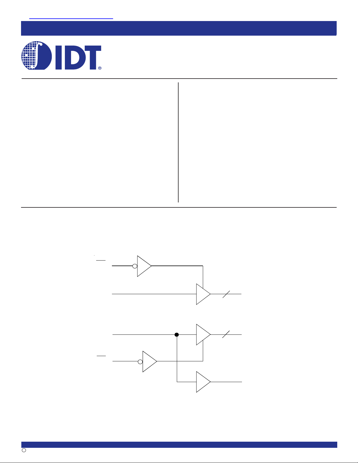
FUNCTIONAL BLOCK DIAGRAM
OH, +48mA IOL
IDT49FCT805BT/CT
DESCRIPTION:
This buffer/clock driver is built using advanced dual metal CMOS
technology. The FCT805T is a non-inverting clock driver consisting of two
banks of drivers. Each bank drives five output buffers from a standard TTL
compatible input. This part has extremely low output skew, pulse skew, and
package skew. The device has a “heart-beat” monitor for diagnostics and
PLL driving. The monitor output is identical to all other outputs and complies
with the output specifications in this document.
The FCT805T is designed for fast, clean edge rates to provide accurate
clock distribution in high speed systems.
OEA
INA
IN B
OEB
The IDT logo is a registered trademark of Integrated Device Technology, Inc.
MILITARY AND COMMERCIAL TEMPERATURE RANGES
2000 Integrated Device Technology, Inc. DSC-4771/2c
1
5
OA1-O A 5
5
OB1-O B 5
MON
JULY 2000
IDT49FCT805BT/CT
FAST CMOS BUFFER/CLOCK DRIVER
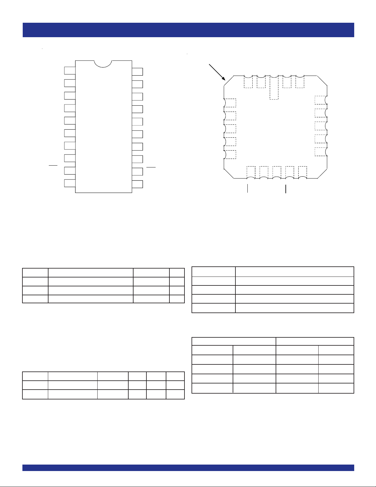
PIN CONFIGURATION
MILITARY AND COMMERCIAL TEMPERATURE RANGES
VCC
OA1
OA2
OA3
GND
OA4
OA5
(1)
GND
OEA
INA
NOTE:
1. Pin 8 is internally connected to GND. To insure compatibility with all products, pin
8 should be connected to GND at the board level.
2
3
4
5
6
7
8
9
10
QSOP/ SOIC/ SSOP/ CERDIP
TOP VIEW
201
19
18
17
16
15
14
13
12
11
VCC
OB1
OB2
OB3
GND
OB4
OB5
MON
OEB
B
IN
INDEX
GND
OA
GND
OA4
OA5
(1)
2
1
C
C
A
A
O
3
3
4
V
O
2
20
1
5
6
7
8
1
C
C
B
V
O
19
18
17
16
15
14
OB2
OB3
GND
OB4
OB5
9 10111213
A
E
O
TOP VIEW
A
N
I
LCC
B
B
N
I
E
O
N
O
M
ABSOLUTE MAXIMUM RATINGS
Symbol Description Ma x Unit
VTERM Terminal Voltage with Respect to GND –0.5 to +7 V
TSTG Storage Temperature –65 to +150 °C
IOUT DC Output Current –60 to +120 mA
NOTE:
1. Stresses greater than those listed under ABSOLUTE MAXIMUM RATINGS may cause
permanent damage to the device. This is a stress rating only and functional operation
of the device at these or any other conditions above those indicated in the operational
sections of this specification is not implied. Exposure to absolute maximum rating
conditions for extended periods may affect reliability.
(1)
CAPACITANCE (TA = +25OC, f = 1.0MHz)
Symbol Parameter
CIN Input Capacitance VIN = 0V 4.5 6 pF
COUT Output Capacitance VOUT = 0V 5.5 8 pF
NOTE:
1. This parameter is measured at characterization but not tested.
(1)
Conditions Typ. Max. Unit
PIN DESCRIPTION
Pin Names Description
OEA, OEB 3-State Output Enable Inputs (Active LOW)
INA, INB Clock Inputs
OAx, OBx Clock Outputs
MON Monitor Output
FUNCTION T ABLE
Inputs Outputs
OEA, OEB INA, INB OAx, OBx MON
LLLL
LHHH
HLZL
HHZH
NOTE:
1. H = HIGH
L = LOW
Z = High-Impedance
(1)
2
IDT49FCT805BT/CT
FAST CMOS BUFFER/CLOCK DRIVER
MILITARY AND COMMERCIAL TEMPERATURE RANGES
DC ELECTRICAL CHARACTERISTICS OVER OPERATING RANGE
Following Conditions Apply Unless Otherwise Specified:
Commercial: TA = 0°C to +70°C, Military: TA = -55°C to +125°C, VCC = 5V ± 10%
Symbol Parameter Test Conditions
(1)
Min. Typ.
VIH Input HIGH Level Guaranteed Logic HIGH Level 2 — — V
VIL Input LOW Level Guaranteed Logic LOW Level — — 0.8 V
IIH Input HIGH Current
IIL Input LOW Current
OZH High Impedance Output Current VCC = Max. VO = 2.7V — — ±1µA
I
(5)
(5)
VCC = Max. VI = 2.7V — — ±1µA
VCC = Max. VI = 0.5V — — ±1µA
IOZL (3-State Output Pins) VO = 0.5V — — ±1
II Input HIGH Current VCC = Max., VI = VCC (Max.) — — ±1µA
VIK Clamp Diode Voltage VCC = Min., IIN = –18mA — –0.7 –1.2 V
IOS Short Circuit Current VCC = Max., VO = GND
CC = Min. IOH = –12mA MIL 2.4 3.3 — V
V
V
OH Output HIGH Voltage VIN = VIH or VIL IOH = –15mA COM'L
(3)
–60 –120 –255 mA
IOH = –24mA MIL 2 3 — V
IOH = –32mA COM'L
(4)
VOL Output LOW Voltage VCC = Min. IOL = 32mA MIL — 0.3 0.55 V
VIN = VIH or VIL IOL = 48mA COM'L
IOFF Input/Output Power Off Leakage
(5)
VCC = 0V, VIN or VO ≤ 4.5V — — ±1µA
VH Input Hysteresis for all inputs — — 15 0 — mV
ICCL Quiescent Power Supply Current VCC = Max., VIN = GND or VCC — 5 500 µA
ICCH
ICCZ
(2)
Max. Unit
NOTES:
1. For conditions shown as Max. or Min., use appropriate value specified under Electrical Characteristics for the applicable device type.
2. Typical values are at Vcc = 5V, +25°C ambient.
3. Not more than one output should be shorted at one time. Duration of the test should not exceed one second.
4. Duration of the condition should not exceed one second.
5. The test limit for this parameter is ±5µA at TA = -55°C.
3
 Loading...