

PRELIMINARY DATASHEET
27 MHZ FIXED AND SPREAD CLOCK GENERATOR ICS8OSK270
Description
The ICS8OSK270 is a low cost integrated clock
synthesizer solution replacing crystals and crystal
oscillators.
The ICS8OSK270 generates a very accurate 27.00
MHz fixed clock output, and a 27.00 MHz spread
spectrum clock output from a 14.31818 MHz reference
clock or crystal input.
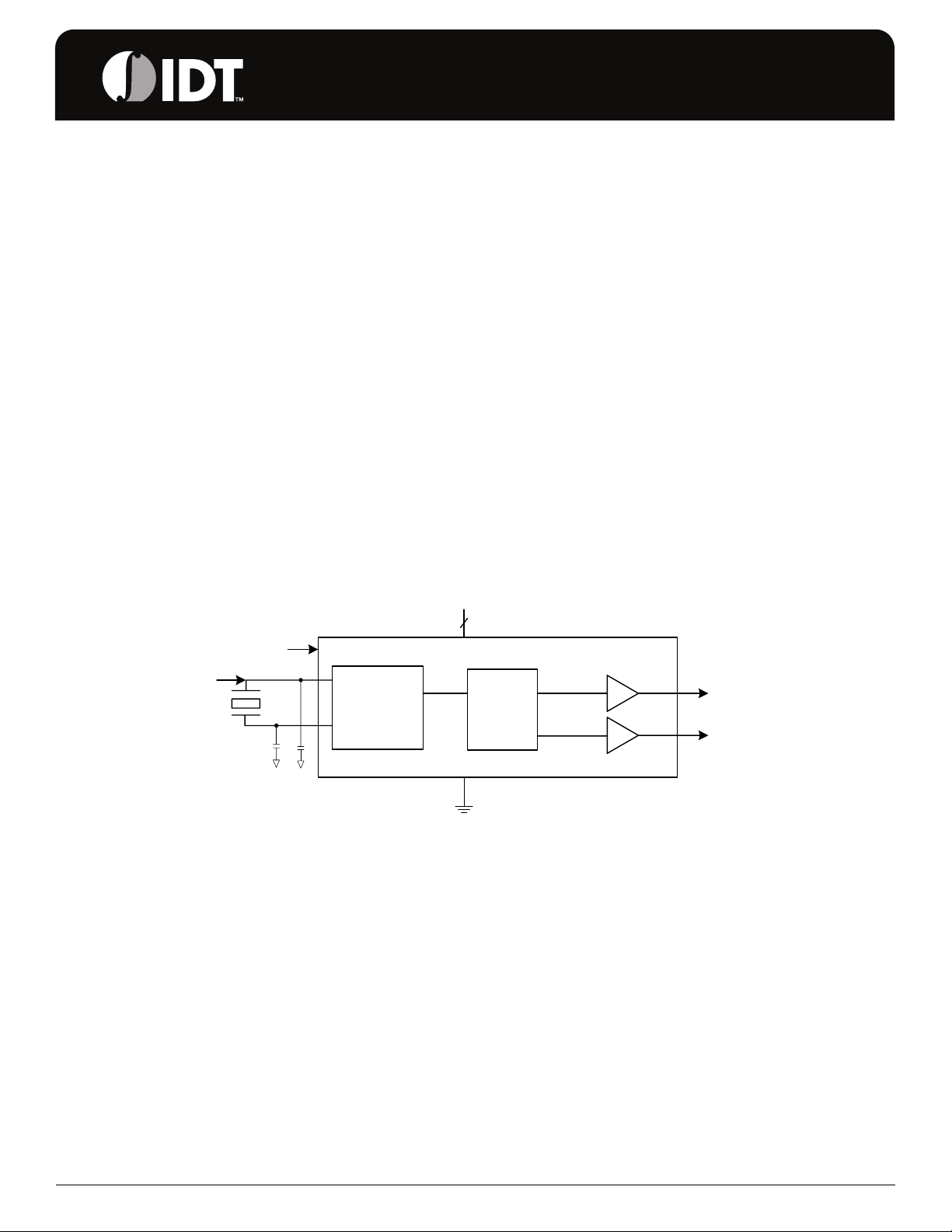
Block Diagram
14.318 MHz
crystal or clock
input
X1/ICLK
X2
S0
Crystal
Oscillator/
Clock Buffer
VDD
Features
• 14.31818 MHz crystal or clock input
• The 27 MHz_Fixed clock output is non-spread with
<10 ppm synthesis error
• 27 MHz_SS clock output with selectable spread
spectrum for EMI reduction
• Output duty cycle 45/55% (worst case)
• Advanced, low-power CMOS process
• Industrial temperature range (-40 to 85°C)
• Packaged in 8-pin MSOP (3.00 mm body)
• RoHS 5 (green) or RoHS 6 (green and lead free)
compliant packaging
2
27M_Fixed
PLL
27M_SS
IDT™ / ICS™
External capacitors are
required with a crystal input
GND
27 MHZ FIXED AND SPREAD CLOCK GENERATOR 1
ICS8OSK270 REV C 050406
ICS8OSK270
27 MHZ FIXED AND SPREAD CLOCK GENERATOR SSCG
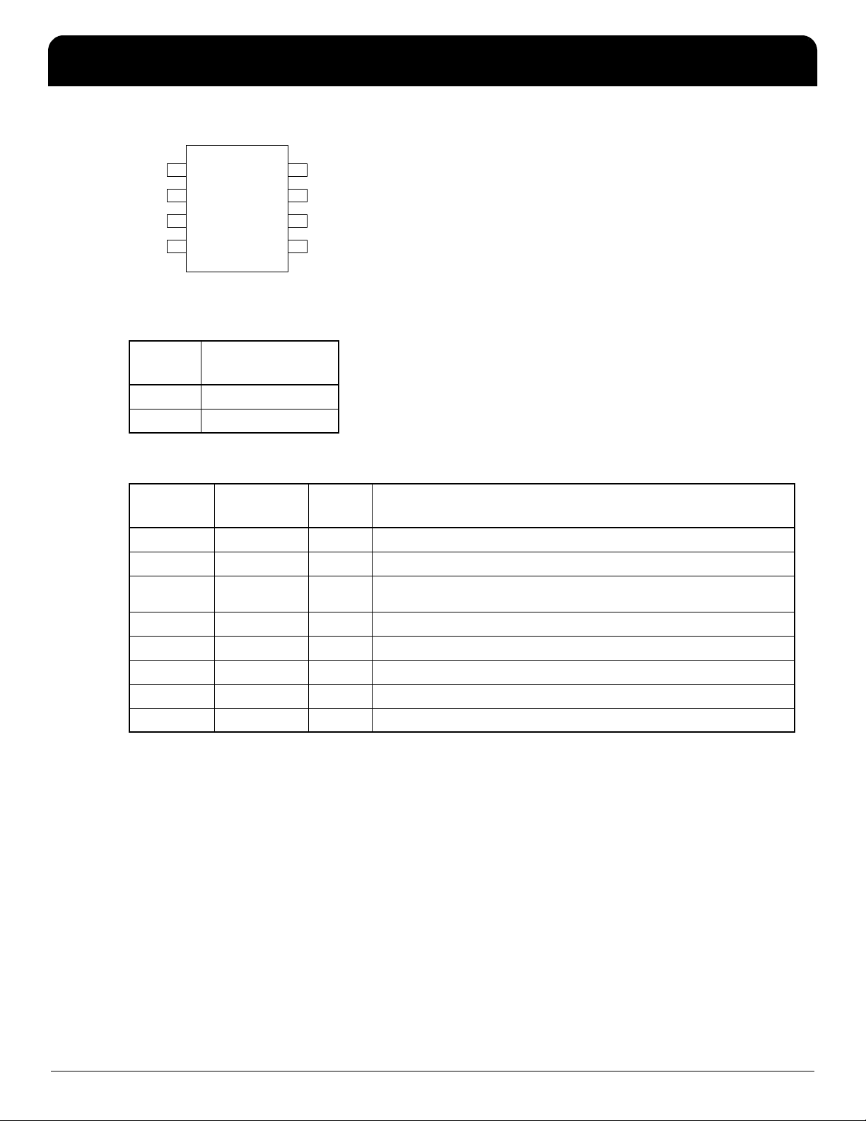
Pin Assignment
8
S0
1
VDD
VDD
X1/I CLK
X2
2
3
4
7
6
5
GND
27M_SS
27M_FIXED
Spread Spectrum Percentage Selection Table
S0 27M_SS Down
Spread
0 -0.5%
1 -1.5%
Pin Descriptions
Pin
Number
1 S0 Input Spread Spectrum percentage select 0. See table above.
2 VDD Power Connect to +3.3 V.
3 X1/ICLK Input Crystal connection. Connect to14.31818 MHz crystal or clock
4 X2 Output Crystal connection. Connect to14.31818 MHz crystal.
Pin
Name
Pin
Typ e
input.
Pin Description
5 27M_FIXED Output 27 MHz fixed clock output at 3.3 V.
6 27M_SS Output 27 MHz spread spectrum clock output at 3.3 V.
7 GND Power Connect to ground.
8 VDD Power Connect to +3.3 V.
IDT™ / ICS™
27 MHZ FIXED AND SPREAD CLOCK GENERATOR 2
ICS8OSK270 REV C 050406

ICS8OSK270
27 MHZ FIXED AND SPREAD CLOCK GENERATOR SSCG
External Components
Decoupling Capacitor
As with any high-performance mixed-signal IC, the
ICS8OSK270 must be isolated from system power
supply noise to perform optimally.
A decoupling capacitor of 0.01µF must be connected
between each VDD and the PCB ground plane.
Series Termination Resistor
Clock output traces over one inch should use series
termination. To series terminate a 50Ω trace (a
commonly used trace impedance), place a 33Ω resistor
in series with the clock line, as close to the clock output
pin as possible. The nominal impedance of the clock
output is 20Ω.
Crystal Load Capacitors
The device crystal connections should include pads for
small capacitors from X1 to ground and from X2 to
ground. These capacitors are used to adjust the stray
capacitance of the board to match the nominally
required crystal load capacitance. Because load
capacitance can only be increased in this trimming
process, it is important to keep stray capacitance to a
minimum by using very short PCB traces (and no vias)
between the crystal and device. Crystal capacitors must
be connected from each of the pins X1 and X2 to
ground.
PCB Layout Recommendations
For optimum device performance and lowest output
phase noise, the following guidelines should be
observed.
1) The 0.01µF decoupling capacitors should be
mounted on the component side of the board as close
to the VDD pin as possible. No vias should be used
between the decoupling capacitors and VDD pins. The
PCB trace to VDD pins should be kept as short as
possible, as should the PCB trace to the ground via.
2) The external crystal should be mounted just next to
the device with short traces. The X1 and X2 traces
should not be routed next to each other with minimum
spaces, instead they should be separated and away
from other traces.
3) To minimize EMI, the 33Ω series termination resistor
(if needed) should be placed close to the clock output.
4) An optimum layout is one with all components on the
same side of the board, minimizing vias through other
signal layers. Other signal traces should be routed away
from the ICS8OSK270. This includes signal traces just
underneath the device, or on layers adjacent to the
ground plane layer used by the device.
The value (in pF) of these crystal caps should equal (C
-6 pF)*2. In this equation, C
in pF. Example: For a crystal with a 16 pF load
capacitance, each crystal capacitor would be 20 pF
[(16-6) x 2 = 20].
IDT™ / ICS™
27 MHZ FIXED AND SPREAD CLOCK GENERATOR 3
= crystal load capacitance
L
L
ICS8OSK270 REV C 050406

ICS8OSK270
27 MHZ FIXED AND SPREAD CLOCK GENERATOR SSCG
Absolute Maximum Ratings
Stresses above the ratings listed below can cause permanent damage to the ICS8OSK270. These ratings,
which are standard values for ICS commercially rated parts, are stress ratings only. Functional operation of
the device at these or any other conditions above those indicated in the operational sections of the
specifications is not implied. Exposure to absolute maximum rating conditions for extended periods can
affect product reliability. Electrical parameters are guaranteed only over the recommended operating
temperature range.
Item Rating
Supply Voltage, VDD -0.5 V to 7 V
All Inputs -0.5 V to VDD+0.5 V
All Outputs -0.5 V to 2.5V+0.5 V
Storage Temperature -65 to +150°C
Junction Temperature 125°C
Soldering Temperature 260°C
ESD (HBM) 2000V min.
MSL (Moisture Sensitivity Level) 3
Recommended Operation Conditions
Parameter Min. Typ. Max. Units
Ambient Operating Temperature -40 +85 °C
Power Supply Voltage (measured in respect to GND) +3.135 +3.465 V
DC Electrical Characteristics
Unless stated otherwise, VDD = 3.3 V ±5%, Ambient Temp -40°C to +85°C
Parameter Symbol Conditions Min. Typ. Max. Units
Operating Voltage VDD 3.135 3.465 V
Supply Current IDD
Input High Voltage V
Input Low Voltage V
Output High Voltage V
Output Low Voltage V
Load Capacitance,
OH
OL
C
X1 and X2
No load
IH
IL
I
= -25 mA 2.4 V
OH
IOL = +25 mA 0.4 V
No internal load
L
capacitance
30 mA
2V
0.8 V
5pF
IDT™ / ICS™
27 MHZ FIXED AND SPREAD CLOCK GENERATOR 4
ICS8OSK270 REV C 050406

ICS8OSK270
27 MHZ FIXED AND SPREAD CLOCK GENERATOR SSCG
AC Electrical Characteristics
Unless stated otherwise, VDD = 3.3 V ±5%, Ambient Temperature -40°C to +85°C
Parameter Symbol Conditions Min. Typ. Max. Units
Input Frequency f
Output Rise Time t
Output Fall Time t
Output Impedance R
IN
OR
OF
20% to 80%, Note 1 0.7 1.0 2.2 ns
80% to 20%, Note 1 0.7 1.0 2.2 ns
VO=VDD/2 20 Ω
O
Output Clock Duty Cycle VDD/2, Note 1 45 50 55 %
Frequency Synthesis Error 27M_FIXED 10 ppm
Short Term Jitter Cycle-to-Cycle 100 200 ps
Long Term Jitter 27M_FIXED, n=1000 200 400 ps
Power-up Time t
PU
From minimum VDD to
outputs stable
Note 1: Measured with a 15 pF load.
14.31818
MHz
13ms
IDT™ / ICS™
27 MHZ FIXED AND SPREAD CLOCK GENERATOR 5
ICS8OSK270 REV C 050406

ICS8OSK270
27 MHZ FIXED AND SPREAD CLOCK GENERATOR SSCG
Package Outline and Package Dimensions (8-pin MSOP, 3.00 mm Body)
Package dimensions are kept current with JEDEC Publication No. 95
IND EX
AREA
8
Symbol Min Max Min Max
Millimeters Inches*
A--1.10--0.043
A1 00.1500.006
E1
E
A2 0.79 0.97 0.031 0.038
b 0.22 0.38 0.008 0.015
C 0.08 0.23 0.003 0.009
D 3.00 BASIC 0.118 BASIC
E 4.90 BASIC 0.193 BASIC
1 2
E1 3.00 BASIC 0.118 BASIC
e 0.65 Basic 0.0256 Basic
D
L 0.40 0.80 0.016 0.032
α 0° 8° 0° 8°
aaa - 0.10 - 0.004
*For reference only. Controlling dimensions in mm.
A
2
A
A
1
- C -
c
e
b
SEATING
PLANE
aaa
L
C
Ordering Information
Part / Order Number Marking Shipping Packaging Package Temperature
ICS8OSK270GILF TBD Tubes 8-pin MSOP -40 to +85° C
ICS8OSK270GILFT Tape and Reel 8-pin MSOP -40 to +85° C
Parts that are ordered with a “LF” suffix to the part number are the Pb-Free configuration and are RoHS compliant.
While the information presented herein has been checked for both accuracy and reliability, Integrated Circuit Systems (ICS)
assumes no responsibility for either its use or for the infringement of any patents or other rights of third parties, which would
result from its use. No other circuits, patents, or licenses are implied. This product is intended for use in normal commercial
applications. Any other applications such as those requiring extended temperature range, high reliability, or other extraordinary
environmental requirements are not recommended without additional processing by ICS. ICS reserves the right to change any
circuitry or specifications without notice. ICS does not authorize or warrant any ICS product for use in life support devices or
critical medical instruments.
IDT™ / ICS™
27 MHZ FIXED AND SPREAD CLOCK GENERATOR 6
ICS8OSK270 REV C 050406

ICS8OSK270
27 MHZ FIXED AND SPREAD CLOCK GENERATOR SSCG
Revision History
Rev. Originator Date Description of Change
A J.Sarma 03/02/06 Released from Proposal to Preliminary; added TSSOP package information.
B J.Sarma 03/08/06 Corrected the part number. The 8MSOP package part is the ICS8OSK270AGILF and the
8TSSOP package part is the ICS8OSK270GILF.
C J.Sarma 05/04/06 Deleted the TSSOP package availability–8MSOP package only.
IDT™ / ICS™
27 MHZ FIXED AND SPREAD CLOCK GENERATOR 7
ICS8OSK270 REV C 050406

ICS8OSK270
27 MHZ FIXED AND SPREAD CLOCK GENERATOR SSCG
Innovate with IDT and accelerate your future networks. Contact:
www.IDT.com
For Sales
800-345-7015
408-284-8200
Fax: 408-284-2775
Corporate Headquarters
Integrated Device Technology, Inc.
6024 Silver Creek Valley Road
San Jose, CA 95138
United States
800 345 7015
+408 284 8200 (outside U.S.)
© 2006 Integrated Device Technology, Inc. All rights reserved. Product specifications subject to change without notice. IDT an d the IDT logo are trademarks of Integrated Device
Technology, Inc. Accelerated Thinking is a service mark of Integrated Device Technology, Inc. All other brands, product names and marks are o r may be trademarks or registered
trademarks used to identify products or services of their respective owners.
Printed in USA
For Tech Support
<product line email>
<product line phone>
Asia Pacific and Japan
Integrated Device Technology
Singapore (1997) Pte. Ltd.
Reg. No. 199707558G
435 Orchard Road
#20-03 Wisma Atria
Singapore 238877
+65 6 887 5505
Europe
IDT Europe, Limited
Prime House
Barnett Wood Lane
Leatherhead, Surrey
United Kingdom KT22 7DE
+44 1372 363 339

 Loading...