

PRELIMINARY
LOW SKEW, DUAL, 1-TO-2 DIFFERENTIALTO-LVDS, LVPECL FANOUT BUFFER
GENERAL DESCRIPTION
ICS
HiPerClockS™
differential input levels. The ICS854S204I is characterized to
operate from either a 2.5V or a 3.3V power supply. Guaranteed output and bank skew characteristics make the
ICS854S204I ideal for those clock distribution applications
demanding well defined performance and repeatability.
SUPPLY MODE OPERATION T ABLE
V
The ICS854S204I is a l ow skew, high performance
dual, 1-to-2 Differential-to-LVDS, LVPECL Fanout
Buffer and a member of the HiPerClockS™ fam-
ily of High Performance Clock Solutions from IDT.
The CLKx, nCLKx pairs can accept most standard
noitarepOV3.3noitarepOV5.2
V3.3=V
DD
V
cn=V
PAT
V5.2=
DD
V5.2=
PAT
ICS854S204I
FEATURES
• Two differential LVDS or LVPECL output banks
• Two differential clock input pairs
• CLKx, nCLKx pairs can accept the following differential
input levels: LVDS, LVPECL, LVHSTL, SSTL, HCSL
• Maximum output frequency: >3GHz
• Translates any single ended input signal to LVDS levels
with resistor bias on nCLKx inputs
• Output skew: <25ps (typical) design target
• Bank skew: <50ps (typical) design target
• Propagation delay: TBD
• Additive phase jitter, RMS: 0.15ps (typical)
• Full 3.3V or 2.5V power supply
• -40°C to 85°C ambient operating temperature
• Available in both standard (RoHS 5) and lead-free (RoHS 6)
packages
SEL_OUT FUNCTION TABLE
TUO_LESleveLtuptuO
0SDVL
1LCEPVL
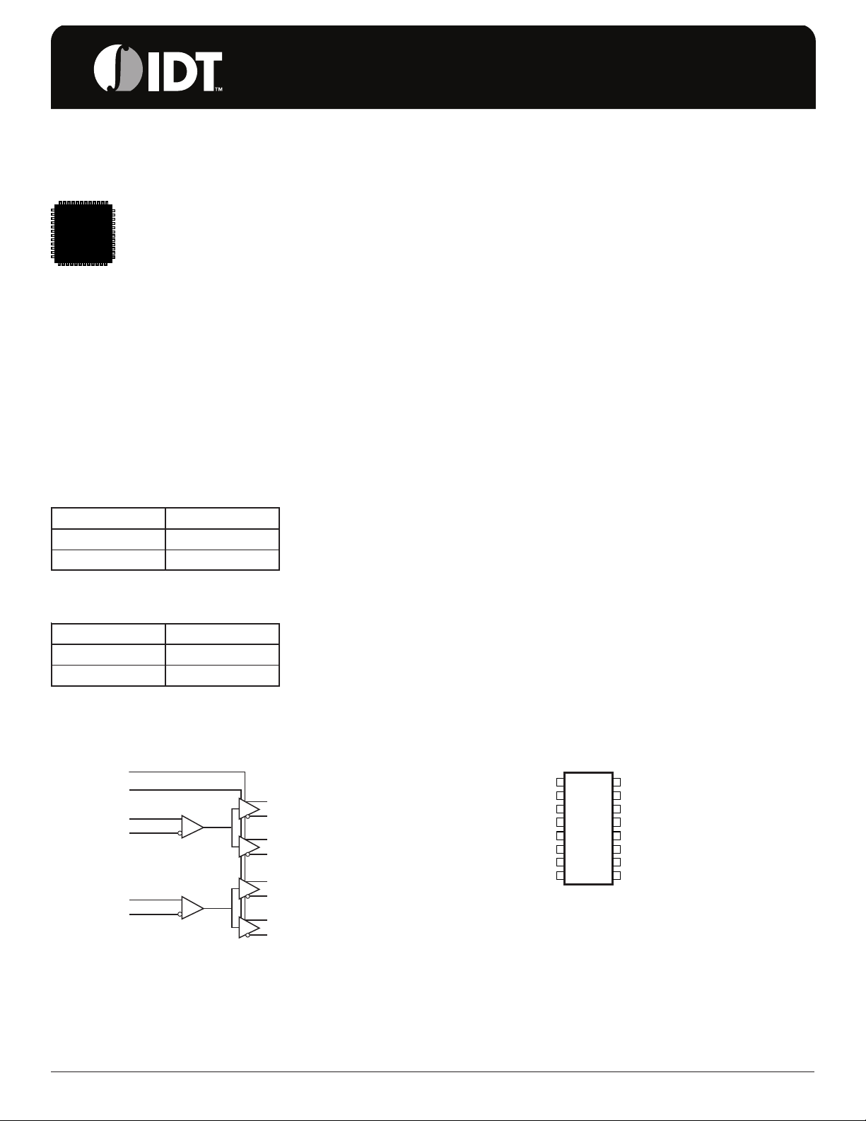
BLOCK DIAGRAM PIN ASSIGNMENT
V
TAP
CLKA
nCLKA
CLKB
nCLKB
Pulldown
Pulldown
Pullup
Pulldown
Pullup
QA0
nQA0
QA1
nQA1
QB0
nQB0
QB1
nQB1
nCLKA
4.4mm x 5.0mm x 0.92mm package body
SEL_OUT
The Preliminary Information presented herein represents a product in prototyping or pre-production. The noted characteristics are based on initial product
characterization. Integrated Device Technology, Incorporated (IDT) reserves the right to change any circuitry or specifications without notice.
1
CLKA
QA0
nQA0
QA1
nQA1
V
TAP
GND
16
2
15
3
14
4
13
5
12
6
11
7
10
8
9
ICS854S204I
16-Lead TSSOP
G Package
Top View
nCLKB
CLKB
QB0
nQB0
QB1
nQB1
V
DD
SEL_OUT
IDT™ / ICS™ LVDS, LVPECL FANOUT BUFFER 1 ICS854S204AGI REV A AUGUST 14, 2006
ICS854S204I
LOW SKEW, DUAL, 1-TO-2 DIFFERENTIAL-TO-LVDS, LVPECL FANOUT BUFFER PRELIMINARY
TABLE 1. PIN DESCRIPTIONS
rebmuNemaNepyTnoitpircseD
1AKLCtupnInwodlluP.tupnikcolclaitnereffidgnitrevni-noN
2AKLCntupnIpulluP.tupnikcolclaitnereffidgnitrevnI
4,30AQn,0AQtuptuO .slevelecafretniLCEPVLroSDVL.riaptuptuolaitnereffiD
6,51AQn,1AQtuptuO .slevelecafretniLCEPVLroSDVL.riaptuptuolaitnereffiD
7V
PAT
rewoPVoteiT.nipylppusrewoP
8DNGrewoP.dnuorgylppusrewoP
9TUO_LEStupnInwodlluP.stuptuoLCEPVLroSDVLneewtebstceleS
01V
DD
rewoP.nipylppusrewoP
21,111BQ,1BQntuptuO .slevelecafretniLCEPVLroSDVL.riaptuptuolaitnereffiD
41,310BQ,0BQntuptuO .slevelecafretniLCEPVLroSDVL.riaptuptuolaitnereffiD
51BKLCtupnInwodlluP.tupnikcolclaitnereffidgnitrevni-noN
61BKLCntupnIpulluP.tupnikcolclaitnereffidgnitrevnI
pulluP
:ETON
dna
nwodlluP
DD
.noitarepoV5.2rof
.seulavlacipytrof,scitsiretcarahCniP,2elbaTeeS.srotsisertupnilanretniotrefer
TABLE 2. PIN CHARACTERISTICS
lobmySretemaraPsnoitidnoCtseTmuminiMlacipyTmumixaMstinU
C
NI
R
PULLUP
R
NWODLLUP
ecnaticapaCtupnI 4Fp
rotsiseRpulluPtupnI 15kΩ
rotsiseRnwodlluPtupnI 15kΩ
TABLE 3. CLOCK INPUT FUNCTION TABLE
stupnIstuptuO
BKLCroAKLCBKLCnroAKLCn
01WOLHGIHlaitnereffiDotlaitnereffiDgnitrevnInoN
10 HGIHWOLlaitnereffiDotlaitnereffiDgnitrevnInoN
01ETON;desaiBWOLHGIHlaitnereffiDotdednEelgniSgnitrevnInoN
11ETON;desaiBHGIHWOLlaitnereffiDotdednEelgniSgnitrevnInoN
1ETON;desaiB0HGIHWOLlaitnereffiDotdednEelgniSgnitrevnI
1ETON;desaiB1WOLHGIHlaitnereffiDotdednEelgniSgnitrevnI
,1AQ,0AQ
1BQ,0BQ
,1AQn,0AQn
1BQn,0BQn
edoMtuptuOottupnIytiraloP
."sleveLdednEelgniStpeccAottupnIlaitnereffiDehtgniriW",noitamrofnInoitacilppAehtotreferesaelP:1ETON
IDT™ / ICS™ LVDS, LVPECL FANOUT BUFFER 2 ICS854S204AGI REV A AUGUST 14, 2006
ICS854S204I
LOW SKEW, DUAL, 1-TO-2 DIFFERENTIAL-TO-LVDS, LVPECL FANOUT BUFFER PRELIMINARY
ABSOLUTE MAXIMUM RATINGS
Supply Voltage, V
Inputs, V
Outputs, I
I
O
(LVPECL)
DD
4.6V
-0.5V to V
+ 0.5 V
DD
Continuous Current 50mA
Surge Current 100mA
Outputs, I
(LVDS)
O
Continuous Current 10mA
Surge Current 15mA
Package Thermal Impedance, θ
Storage Temperature, T
(Junction-to-Ambient)
STG
89°C/W (0 lfpm)
JA
-65°C to 150°C
TABLE 4A. LVDS POWER SUPPLY DC CHARACTERISTICS, V
lobmySretemaraPsnoitidnoCtseTmuminiMlacipyTmumixaMstinU
V
DD
I
DD
egatloVylppuSrewoP 531.33.3564.3V
tnerruCylppuSrewoP 001Am
NOTE: Stresses beyond those listed under Absolute
Maximum Ratings may cause permanent damage to the
device. These ratings are stress specifications only. Functional operation of product at these conditions or any conditions beyond
those listed in the
implied. Exposure to absolute maximum rating conditions for extended periods may affect product reliability.
= 3.3V±5%, TA = -40°C TO 85°C
DD
DC Characteristics
or
AC Characteristics
is not
TABLE 4B. LVDS POWER SUPPLY DC CHARACTERISTICS, V
DD
lobmySretemaraPsnoitidnoCtseTmuminiMlacipyTmumixaMstinU
V
DD
V
PAT
I
DD
I
PAT
egatloVylppuSrewoP 573.25.2526.2V
egatloVylppuSrewoP 573.25.2526.2V
tnerruCylppuSrewoP 59Am
tnerruCylppuSrewoP 5Am
TABLE 4C. LVPECL POWER SUPPLY DC CHARACTERISTICS, V
lobmySretemaraPsnoitidnoCtseTmuminiMlacipyTmumixaMstinU
V
DD
I
DD
egatloVylppuSrewoP 531.33.3564.3V
tnerruCylppuSrewoP 001Am
TABLE 4D. LVPECL POWER SUPPLY DC CHARACTERISTICS, V
lobmySretemaraPsnoitidnoCtseTmuminiMlacipyTmumixaMstinU
V
DD
V
PAT
I
DD
I
PAT
egatloVylppuSrewoP 573.25.2526.2V
egatloVylppuSrewoP 573.25.2526.2V
tnerruCylppuSrewoP 59Am
tnerruCylppuSrewoP 5Am
= V
= 2.5V±5%, TA = -40°C TO 85°C
TAP
= 3.3V±5%, TA = -40°C TO 85°C
DD
= V
DD
= 2.5V±5%, TA = -40°C TO 85°C
TAP
IDT™ / ICS™ LVDS, LVPECL FANOUT BUFFER 3 ICS854S204AGI REV A AUGUST 14, 2006
ICS854S204I
LOW SKEW, DUAL, 1-TO-2 DIFFERENTIAL-TO-LVDS, LVPECL FANOUT BUFFER PRELIMINARY
TABLE 4E. LVCMOS / LVTTL DC CHARACTERISTICS, V
lobmySretemaraPsnoitidnoCtseTmuminiMlacipyTmumixaMstinU
V
HI
V
LI
I
HI
I
LI
TABLE 4F. DIFFERENTIAL DC CHARACTERISTICS, V
lobmySretemaraPsnoitidnoCtseTmuminiMlacipyTmumixaMstinU
I
HI
I
LI
V
PP
V
RMC
2,1ETON
egatloVhgiHtupnI
egatloVwoLtupnI
tnerruChgiHtupnITUO_LESV
tnerruCwoLtupnITUO_LESV
V=
DD
DD
= 3.3V±5% OR VDD = V
DD
,AKLC
BKLC
tnerruChgiHtupnI
,AKLCn
V
BKLCn
,AKLC
BKLC
tnerruCwoLtupnI
,AKLCn
V
BKLCn
egatloVtupnIkaeP-ot-kaeP 51.03.1V
;egatloVtupnIedoMnommoC
.
VsadenifedsiegatlovedomnommoC:1ETON
HI
= 3.3V±5% OR VDD = V
DD
V
V
DD
V
V
DD
NI
V
DD
V3.3=2V
DD
V526.2=7.1V
V3.3=3.0-8.0V
DD
V526.2=3.0-7.0V
V,V526.2ro564.3=
NI
V=
NI
V564.3=
V526.2ro
DD
V
V0=
NI
V=
V
DD
NI
V564.3=
V526.2ro
DD
V0=
V
NI
= 2.5V±5%, TA = -40°C TO 85°C
TAP
3.0+V
CC
3.0+V
CC
V526.2roV564.3=051Aµ
V0=5-Aµ
= 2.5V±5%, TA = -40°C TO 85°C
TAP
051Aµ
,V526.2roV564.3=
5Aµ
5-Aµ
,V526.2roV564.3=
051-Aµ
5.0+DNGV
VsixKLCn,xKLCrofegatlovtupnimumixameht,snoitacilppadedneelgnisroF:2ETON
.V3.0+
58.0-V
DD
TABLE 4G. LVDS DC CHARACTERISTICS, V
= 3.3V±5%, TA = -40°C TO 85°C
DD
lobmySretemaraPsnoitidnoCtseTmuminiMlacipyTmumixaMstinU
V
∆ V
V
∆ V
DO
V
DO
SO
SO
DO
egatloVtesffO0=TUO_LES53.1V
V
SO
egatloVtuptuOlaitnereffiD0=TUO_LES004Vm
egnahCedutingaM0=TUO_LES04Vm
egnahCedutingaM0=TUO_LES05Vm
.noitamrofnituptuorofnoitamrofnItnemerusaeMretemaraPotreferesaelP:ETON
TABLE 4H. LVDS DC CHARACTERISTICS, V
DD
= V
= 2.5V±5%, TA = -40°C TO 85°C
TAP
lobmySretemaraPsnoitidnoCtseTmuminiMlacipyTmumixaMstinU
V
∆ V
V
∆ V
DO
V
DO
SO
SO
DO
egatloVtesffO0=TUO_LES3.1V
V
SO
egatloVtuptuOlaitnereffiD0=TUO_LES073Vm
egnahCedutingaM0=TUO_LES04Vm
egnahCedutingaM0=TUO_LES05Vm
.noitamrofnituptuorofnoitamrofnItnemerusaeMretemaraPotreferesaelP:ETON
IDT™ / ICS™ LVDS, LVPECL FANOUT BUFFER 4 ICS854S204AGI REV A AUGUST 14, 2006
ICS854S204I
LOW SKEW, DUAL, 1-TO-2 DIFFERENTIAL-TO-LVDS, LVPECL FANOUT BUFFER PRELIMINARY
TABLE 4I. LVPECL DC CHARACTERISTICS, V
= 3.3V±5% OR VDD = V
DD
= 2.5V±5%, TA = -40°C TO 85°C
TAP
lobmySretemaraPsnoitidnoCtseTmuminiMlacipyTmumixaMstinU
V
HO
V
LO
V
GNIWS
TABLE 5A. LVDS AC CHARACTERISTICS, V
1ETON;egatloVhgiHtuptuO1=TUO_LESV
1ETON;egatloVwoLtuptuO1=TUO_LESV
4.1-V
DD
0.2-V
DD
gniwSegatloVtuptuOkaeP-ot-kaeP1=TUO_LES6.00.1V
05htiwdetanimretstuptuO:1ETON Ω Vot
.V2-
DD
= 3.3V ± 5%, TA = -40°C TO 85°C
DD
9.0-V
DD
7.1-V
DD
lobmySretemaraPsnoitidnoCtseTmuminiMlacipyTmumixaMstinU
f
t
t
t
t
t
R/tF
XAM
DP
)o(ks4,2ETON;wekStuptuO
)b(ks4,3ETON;wekSknaB
tij
ycneuqerFtuptuO 3>zHG
1ETON;yaleDnoitagaporP DBTsn
52<
tegrat
05<
tegrat
;SMR,rettiJesahPevitiddAreffuB
noitceSrettiJesahPevitiddAotrefer
51.0sp
emiTllaF/esiRtuptuO%08ot%02052sp
sp
sp
cdoelcyCytuDtuptuO 05%
.esiwrehtodetonsselnuzHM005taderusaemsretemarapllA
.tniopgnissorctuptuolaitnereffidehtottniopgnissorctupnilaitnereffidehtmorfderusaeM:1ETON
.snoitidnocdaollauqehtiwdnaegatlovylppusemasehttastuptuoneewtebwekssadenifeD:2ETON
.stniopssorclaitnereffidtuptuoehtmorfderusaeM
.snoitidnocdaollauqehtiwdnaegatlovylppusemasehttastuptuofoknabanihtiwwekssadenifeD:3ETON
.56dradnatSCEDEJhtiwecnadroccanidenifedsiretemarapsihT:4ETON
TABLE 5B. LVDS AC CHARACTERISTICS, V
DD
= V
= 2.5V ± 5%, TA = -40°C TO 85°C
TAP
lobmySretemaraPsnoitidnoCtseTmuminiMlacipyTmumixaMstinU
f
t
t
t
t
t
R/tF
XAM
DP
)o(ks4,2ETON;wekStuptuO
)b(ks4,3ETON;wekSknaB
tij
ycneuqerFtuptuO 3>zHG
1ETON;yaleDnoitagaporP DBTsn
52<
tegrat
05<
tegrat
;SMR,rettiJesahPevitiddAreffuB
noitceSrettiJesahPevitiddAotrefer
31.0sp
emiTllaF/esiRtuptuO%08ot%02052sp
sp
sp
cdoelcyCytuDtuptuO 05%
.esiwrehtodetonsselnuzHM005taderusaemsretemarapllA
.tniopgnissorctuptuolaitnereffidehtottniopgnissorctupnilaitnereffidehtmorfderusaeM:1ETON
.snoitidnocdaollauqehtiwdnaegatlovylppusemasehttastuptuoneewtebwekssadenifeD:2ETON
.stniopssorclaitnereffidtuptuoehtmorfderusaeM
.snoitidnocdaollauqehtiwdnaegatlovylppusemasehttastuptuofoknabanihtiwwekssadenifeD:3ETON
.56dradnatSCEDEJhtiwecnadroccanidenifedsiretemarapsihT:4ETON
IDT™ / ICS™ LVDS, LVPECL FANOUT BUFFER 5 ICS854S204AGI REV A AUGUST 14, 2006
ICS854S204I
LOW SKEW, DUAL, 1-TO-2 DIFFERENTIAL-TO-LVDS, LVPECL FANOUT BUFFER PRELIMINARY
TABLE 5C. LVPECL AC CHARACTERISTICS, V
= 3.3V ± 5%, TA = -40°C TO 85°C
DD
lobmySretemaraPsnoitidnoCtseTmuminiMlacipyTmumixaMstinU
f
t
t
t
t
t
R/tF
XAM
DP
)o(ks4,2ETON;wekStuptuO
)b(ks4,3ETON;wekSknaB
tij
ycneuqerFtuptuO 3>zHG
1ETON;yaleDnoitagaporP DBTsn
52<
tegrat
05<
tegrat
;SMR,rettiJesahPevitiddAreffuB
noitceSrettiJesahPevitiddAotrefer
21.0sp
emiTllaF/esiRtuptuO%08ot%02052sp
sp
sp
cdoelcyCytuDtuptuO 05%
.esiwrehtodetonsselnuzHM005taderusaemsretemarapllA
.tniopgnissorctuptuolaitnereffidehtottniopgnissorctupnilaitnereffidehtmorfderusaeM:1ETON
.snoitidnocdaollauqehtiwdnaegatlovylppusemasehttastuptuoneewtebwekssadenifeD:2ETON
.stniopssorclaitnereffidtuptuoehtmorfderusaeM
.snoitidnocdaollauqehtiwdnaegatlovylppusemasehttastuptuofoknabanihtiwwekssadenifeD:3ETON
.56dradnatSCEDEJhtiwecnadroccanidenifedsiretemarapsihT:4ETON
TABLE 5D. LVPECL AC CHARACTERISTICS, V
DD
= V
= 2.5V ± 5%, TA = -40°C TO 85°C
TAP
lobmySretemaraPsnoitidnoCtseTmuminiMlacipyTmumixaMstinU
f
t
t
t
t
t
R/tF
XAM
DP
)o(ks4,2ETON;wekStuptuO
)b(ks4,3ETON;wekSknaB
tij
ycneuqerFtuptuO 3>zHG
1ETON;yaleDnoitagaporP DBTsn
52<
tegrat
05<
tegrat
;SMR,rettiJesahPevitiddAreffuB
noitceSrettiJesahPevitiddAotrefer
70.0sp
emiTllaF/esiRtuptuO%08ot%02052sp
sp
sp
cdoelcyCytuDtuptuO 05%
.esiwrehtodetonsselnuzHM005taderusaemsretemarapllA
.tniopgnissorctuptuolaitnereffidehtottniopgnissorctupnilaitnereffidehtmorfderusaeM:1ETON
.snoitidnocdaollauqehtiwdnaegatlovylppusemasehttastuptuoneewtebwekssadenifeD:2ETON
.stniopssorclaitnereffidtuptuoehtmorfderusaeM
.snoitidnocdaollauqehtiwdnaegatlovylppusemasehttastuptuofoknabanihtiwwekssadenifeD:3ETON
.56dradnatSCEDEJhtiwecnadroccanidenifedsiretemarapsihT:4ETON
IDT™ / ICS™ LVDS, LVPECL FANOUT BUFFER 6 ICS854S204AGI REV A AUGUST 14, 2006

ICS854S204I
SCOPE
Qx
nQx
LVDS
2.5V±5%
POWER SUPPLY
+–
Float GND
LOW SKEW, DUAL, 1-TO-2 DIFFERENTIAL-TO-LVDS, LVPECL FANOUT BUFFER PRELIMINARY
PARAMETER MEASUREMENT INFORMATION
SCOPE
3.3V±5%
POWER SUPPLY
+–
Float GND
V
DD
LVDS
Qx
nQx
V
DD,
V
TAP
2V
V
DD
LVPECL
V
EE
-1.3V±0.165V
V
DD
nCLKA, nCLKB
CLKA, CLKB
GND
2.5V LVDS OUTPUT LOAD AC TEST CIRCUIT3.3V LVDS OUTPUT LOAD AC TEST CIRCUIT
2V
Qx
nQx
SCOPE
V
DD,
V
TAP
LVPECL
V
EE
-0.5V±0.125V
Qx
nQx
SCOPE
2.5V LVPECL OUTPUT LOAD AC TEST CIRCUIT3.3V LVPECL OUTPUT LOAD AC TEST CIRCUIT
nQXx
QXx
V
PP
Cross Points
V
CMR
nQXy
QXy
t
sk(b)
Where X = A or B
DIFFERENTIAL INPUT LEVEL
IDT™ / ICS™ LVDS, LVPECL FANOUT BUFFER 7 ICS854S204AGI REV A AUGUST 14, 2006
BANK SKEW

ICS854S204I
LOW SKEW, DUAL, 1-TO-2 DIFFERENTIAL-TO-LVDS, LVPECL FANOUT BUFFER PRELIMINARY
nQx
Qx
nQy
Qy
OUTPUT SKEW
nQAx,
nQBx
QAx,
QBx
t
sk(o)
tPW
odc = x 100%
t
PERIOD
t
t
PERIOD
PW
nCLKA,
nCLKB
CLKA,
CLKB
nQAx,
nQBx
QAx,
QBx
PROPAGATION DELAY
Clock
Outputs
20%
t
PD
80%
t
R
80%
t
F
20%
V
SWING
OUTPUT RISE/FALL TIMEOUTPUT DUTY CYCLE/PULSE WIDTH/PERIOD
DC Input
V
DD
LV DS
out
➤
out
➤
VOS/∆ V
➤
OS
V
DD
➤
out
➤
DC Input
LVDS
100
DIFFERENTIAL OUTPUT VOLTAGE SETUP
IDT™ / ICS™ LVDS, LVPECL FANOUT BUFFER 8 ICS854S204AGI REV A AUGUST 14, 2006
out
V
/∆ V
OD
OD
➤
OFFSET VOLTAGE SETUP

ICS854S204I
LOW SKEW, DUAL, 1-TO-2 DIFFERENTIAL-TO-LVDS, LVPECL FANOUT BUFFER PRELIMINARY
APPLICATION INFORMATION
WIRING THE DIFFERENTIAL INPUT TO ACCEPT SINGLE ENDED LEVELS
Figure 1
single ended levels. The reference voltage V_REF ~ VDD/2 is
generated by the bias resistors R1, R2 and C1. This bias circuit
should be located as close as possible to the input pin. The ratio
shows how the differential input can be wired to accept
Single Ended Clock Input
of R1 and R2 might need to be adjusted to position the V_REF in
the center of the input voltage swing. For example, if the input
clock swing is only 2.5V and V
and R2/R1 = 0.609.
VDD
R1
1K
CLKx
= 3.3V, V_REF should be 1.25V
DD
V_REF
C1
0.1u R2
FIGURE 1. SINGLE ENDED SIGNAL DRIVING DIFFERENTIAL INPUT
RECOMMENDATIONS FOR UNUSED INPUT AND OUTPUT PINS
INPUTS:
CLK/nCLK INPUT:
For applications not requiring the use of the differential input,
both CLK and nCLK can be left floating. Though not required,
but for additional protection, a 1kΩ resistor can be tied from CLK
to ground.
nCLKx
1K
OUTPUTS:
LVDS OUTPUT
All unused LVDS output pairs can be either left floating or
terminated with 100Ω across. If they are left floating, there should
be no trace attached.
LVPECL O
All unused LVPECL outputs can be left floating. We recommend
that there is no trace attached. Both sides of the differential output
pair should either be left floating or terminated.
UTPUT
IDT™ / ICS™ LVDS, LVPECL FANOUT BUFFER 9 ICS854S204AGI REV A AUGUST 14, 2006

ICS854S204I
LOW SKEW, DUAL, 1-TO-2 DIFFERENTIAL-TO-LVDS, LVPECL FANOUT BUFFER PRELIMINARY
DIFFERENTIAL CLOCK INPUT INTERFACE
The CLK /nCLK accepts LVDS, LVPECL, LVHSTL, SSTL, HCSL
and other differential signals. Both V
V
PP
and V
input requirements. Figures 2A to 2E show interface
CMR
and VOH must meet the
SWING
examples for the HiPerClockS CLK/nCLK input driven by the most
common driver types. The input interfaces suggested here are
examples only. Please consult with the vendor of the driver
component to confirm the driver termination requirements. For
example in
Figure 2A,
the input termination applies for ICS
HiPerClockS LVHSTL drivers. If you are using an LVHSTL driver
from another vendor, use their termination recommendation.
1.8V
LVHSTL
ICS
HiPerClockS
LVHSTL Driver
Zo = 50 Ohm
Zo = 50 Ohm
R1
50
3.3V
CLK
nCLK
HiPerClockS
Input
R2
50
FIGURE 2A. HIPERCLOCKS CLK/nCLK INPUT DRIVEN BY
ICS HIPERCLOCKS LVHSTL DRIVER
3.3V
LVPECL
Zo = 50 Ohm
Zo = 50 Ohm
3.3V
R3
125
R4
125
R1
84
3.3V
CLK
nCLK
HiPerClockS
Input
R2
84
FIGURE 2B. HIPERCLOCKS CLK/nCLK INPUT DRIVEN BY
3.3V LVPECL DRIVER
3.3V
3.3V
LVDS_D river
3.3V
Zo = 50 Ohm
Zo = 50 Ohm
LVPECL
Zo = 50 Ohm
Zo = 50 Ohm
HiPerClockS
Input
CLK
nCLK
Receiv er
3.3V
R1
100
CLK
nCLK
R1
R2
50
50
FIGURE 2C. HIPERCLOCKS CLK/nCLK INPUT DRIVEN BY
3.3V LVPECL DRIVER
3.3V
CLK
nCLK
3.3V
HiPerClockS
Input
3.3V
LVPECL
R5
100 - 200
R5,R6 locate near the driver pin.
Zo = 50 Ohm
Zo = 50 Ohm
R6
100 - 200
R3
R4
125
C1
C2
125
R2
R1
84
84
FIGURE 2D. HIPERCLOCKS CLK/nCLK INPUT DRIVEN BY
3.3V LVDS DRIVER
R3
50
FIGURE 2E. HIPERCLOCKS CLK/nCLK INPUT DRIVEN BY
3.3V LVPECL DRIVER WITH AC COUPLE
IDT™ / ICS™ LVDS, LVPECL FANOUT BUFFER 10 ICS854S204AGI REV A AUGUST 14, 2006

ICS854S204I
LOW SKEW, DUAL, 1-TO-2 DIFFERENTIAL-TO-LVDS, LVPECL FANOUT BUFFER PRELIMINARY
3.3V, 2.5V LVDS DRIVER T ERMINATION
A general LVDS interface is shown in
differential transmission line environment, LVDS drivers
require a matched load termination of 100Ω across near
Figure 3.
In a 100Ω
the receiver input. For a multiple LVDS outputs buffer, if only partial
outputs are used, it is recommended to terminate the
unused outputs.
VDD
LVDS_Driv er
100 Ohm Differential Transmission Line
FIGURE 3. TYPICAL LVDS DRIVER T ERMINATION
TERMINATION FOR 3.3V LVPECL OUTPUTS
The clock layout topology shown below is a typical termination
for LVPECL outputs. The two different layouts mentioned are
recommended only as guidelines.
FOUT and nFOUT are low impedance follower outputs that generate ECL/LVPECL compatible outputs. Therefore, terminating
resistors (DC current path to ground) or current sources must
be used for functionality. These outputs are designed to drive
50Ω transmission lines. Matched impedance techniques should
2.5V or 3. 3V
+
R1
100
-
be used to maximize operating frequency and minimize signal
distortion.
Figures 4A and 4B
show two different layouts which
are recommended only as guidelines. Other suitable clock layouts may exist and it would be recommended that the board
designers simulate to guarantee compatibility across all printed
circuit and clock component process variations.
Z
= 50Ω
o
FOUT
= 50Ω
Z
o
RTT = Z
((V
OH
1
+ VOL) / (VCC – 2)) – 2
50Ω 50Ω
o
RTT
FIN
VCC - 2V
125Ω 125Ω
= 50Ω
Z
o
FOUT FIN
= 50Ω
Z
o
3.3V
84Ω 84Ω
FIGURE 4B. LVPECL OUTPUT TERMINATIONFIGURE 4A. LVPECL OUTPUT TERMINATION
IDT™ / ICS™ LVDS, LVPECL FANOUT BUFFER 11 ICS854S204AGI REV A AUGUST 14, 2006

ICS854S204I
LOW SKEW, DUAL, 1-TO-2 DIFFERENTIAL-TO-LVDS, LVPECL FANOUT BUFFER PRELIMINARY
TERMINATION FOR 2.5V LVPECL OUTPUT
Figure 5A
LVPECL driver. These terminations are equivalent to terminating
50Ω to V
and
Figure 5B
- 2V. For V
CC
show examples of termination for 2.5V
= 2.5V, the V
CC
- 2V is very close to ground
CC
level. The R3 in Figure 5B can be eliminated and the termination
is shown in
Figure 5C.
VCC O=2.5V
2,5V LVPECL
Driver
Zo = 50 Ohm
Zo = 50 Ohm
2.5V
R1
250
R2
62.5
R3
250
R4
62.5
2.5V
+
-
FIGURE 5A. 2.5V LVPECL DRIVER TERMINATION EXAMPLE
VCC O=2.5V
2,5V LVPECL
Driver
Zo = 50 Ohm
Zo = 50 Ohm
R2
R1
50
50
2.5V
+
-
VCCO=2. 5V
2,5V LVPEC L
Driver
Zo = 50 Ohm
Zo = 50 Ohm
R150R2
50
R3
18
2.5V
+
-
FIGURE 5B. 2.5V LVPECL DRIVER TERMINATION EXAMPLE
FIGURE 5C. 2.5V LVPECL TERMINATION EXAMPLE
IDT™ / ICS™ LVDS, LVPECL FANOUT BUFFER 12 ICS854S204AGI REV A AUGUST 14, 2006

ICS854S204I
LOW SKEW, DUAL, 1-TO-2 DIFFERENTIAL-TO-LVDS, LVPECL FANOUT BUFFER PRELIMINARY
RELIABILITY INFORMATION
TABLE 6. θ
VS. AIR FLOW TABLE FOR 16 LEAD TSSOP
JA
θθ
θJA by Velocity (Linear Feet per Minute)
θθ
Single-Layer PCB, JEDEC Standard Test Boards 137.1°C/W 118.2°C/W 106.8°C/W
Multi-Layer PCB, JEDEC Standard Test Boards 89.0°C/W 81.8°C/W 78.1°C/W
NOTE: Most modern PCB designs use multi-layered boards. The data in the second row pertains to most designs.
TRANSISTOR COUNT
The transistor count for ICS854S204I is: 454
0 200 500
IDT™ / ICS™ LVDS, LVPECL FANOUT BUFFER 13 ICS854S204AGI REV A AUGUST 14, 2006

ICS854S204I
LOW SKEW, DUAL, 1-TO-2 DIFFERENTIAL-TO-LVDS, LVPECL FANOUT BUFFER PRELIMINARY
PACKAGE OUTLINE - G SUFFIX FOR 16 LEAD TSSOP
T
ABLE 7. PACKAGE DIMENSIONS
LOBMYS
N61
A--02.1
1A50.051.0
2A08.050.1
b91.003.0
c90.002.0
D09.401.5
ECISAB04.6
1E03.405.4
eCISAB56.0
L54.057.0
α
aaa--01.0
Reference Document: JEDEC Publication 95, MO-153
muminiMmumixaM
°0°8
sretemilliM
IDT™ / ICS™ LVDS, LVPECL FANOUT BUFFER 14 ICS854S204AGI REV A AUGUST 14, 2006

ICS854S204I
LOW SKEW, DUAL, 1-TO-2 DIFFERENTIAL-TO-LVDS, LVPECL FANOUT BUFFER PRELIMINARY
TABLE 8. ORDERING INFORMATION
rebmuNredrO/traPgnikraMegakcaPgnigakcaPgnippihSerutarepmeT
IGA402S458SCIIA402S45POSSTdael61ebutC°58otC°04-
TIGA402S458SCIIA402S45POSSTdael61leer&epat0052C°58otC°04-
FLIGA402S458SCILIA402S4POSST"eerF-daeL"dael61ebutC°58otC°04-
TFLIGA402S458SCILIA402S4POSST"eerF-daeL"dael61leer&epat0052C°58otC°04-
.tnailpmocSHoReradnanoitarugifnoceerF-bPehterarebmuntrapehtotxiffus"FL"nahtiwderedroeratahtstraP:ETON
While the information presented herein has been checked for both accuracy and reliability, Integrated Device Technology, Incorporated (IDT) assumes no responsibility for either its use or for
infringement of any patents or other rights of third parties, which would result from its use. No other circuits, patents, or licenses are implied. This product is intended for use in normal commercial and
industrial applications. Any other applications such as those requiring high reliability or other extraordinary environmental requirements are not recommended without additional processing by IDT. IDT
reserves the right to change any circuitry or specifications without notice. IDT does not authorize or warrant any IDT product for use in life support devices or critical medical instruments.
IDT™ / ICS™ LVDS, LVPECL FANOUT BUFFER 15 ICS854S204AGI REV A AUGUST 14, 2006

ICS854S204I
LOW SKEW, DUAL, 1-TO-2 DIFFERENTIAL-TO-LVDS, LVPECL FANOUT BUFFER PRELIMINARY
Innovate with IDT and accelerate your future networks. Contact:
www.IDT.com
For Sales
800-345-7015
408-284-8200
Fax: 408-284-2775
Corporate Headquarters
Integrated Device Technology, Inc.
6024 Silver Creek Valley Road
San Jose, CA 95138
United States
800 345 7015
+408 284 8200 (outside U.S.)
© 2006 Integrated Device Technology, Inc. All rights reserved. Product specifications subject to change without notice. IDT, the IDT logo, ICS and HiPerClockS are trademarks
of Integrated Device Technology, Inc. Accelerated Thinking is a service mark of Integrated Device Technology, Inc. All other brands, product names and marks are or may be
trademarks or registered trademarks used to identify products or services of their respective owners.
Printed in USA
For Tech Support
netcom@idt.com
480-763-2056
Asia Pacific and Japan
Integrated Device Technology
Singapore (1997) Pte. Ltd.
Reg. No. 199707558G
435 Orchard Road
#20-03 Wisma Atria
Singapore 238877
+65 6 887 5505
Europe
IDT Europe, Limited
321 Kingston Road
Leatherhead, Surrey
KT22 7TU
England
+44 (0) 1372 363 339
Fax: +44 (0) 1372 378851

 Loading...