

Integrated Device Technology Inc 7429FCT521DTSOB, 7429FCT521DTSO, 7429FCT521DTQB, 7429FCT521DTQ, 7429FCT521CTSO Datasheet
...
Integrated Device Technology, Inc.
The IDT logo is a registered trademark of Integrated Device Technology, Inc.
DESCRIPTION:
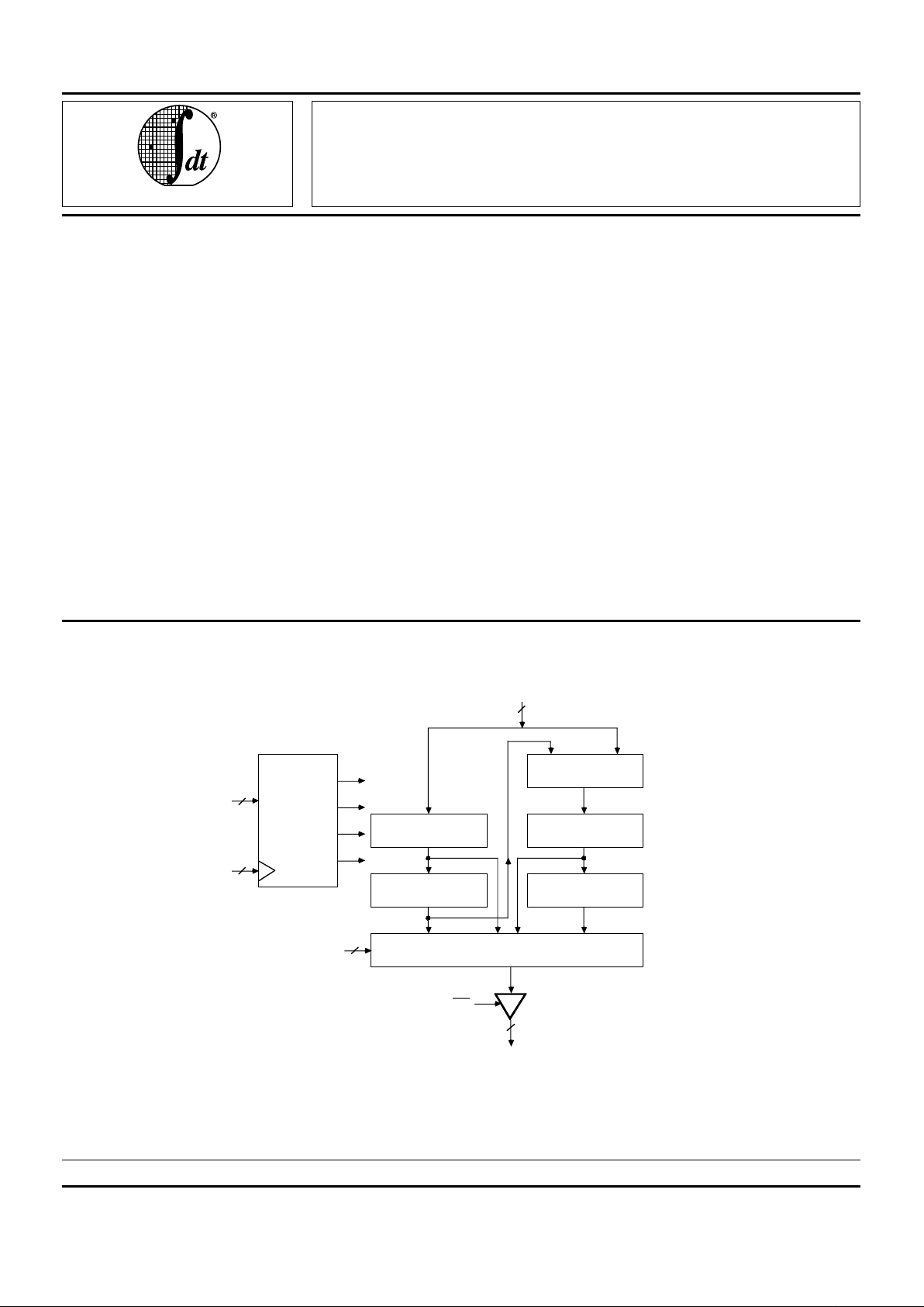
The IDT29FCT520AT/BT/CT/DT and IDT29FCT521AT/
BT/CT/DT each contain four 8-bit positive edge-triggered
registers. These may be operated as a dual 2-level or as a
single 4-level pipeline. A single 8-bit input is provided and any
of the four registers is available at the 8-bit, 3-state output.
These devices differ only in the way data is loaded into and
between the registers in 2-level operation. The difference is
illustrated in Figure 1. In the IDT29FCT520AT/BT/CT/DT
when data is entered into the first level (I = 2 or I = 1), the
existing data in the first level is moved to the second level. In
the IDT29FCT521AT/BT/CT/DT, these instructions simply
cause the data in the first level to be overwritten. Transfer of
data to the second level is achieved using the 4-level shift
instruction (I = 0). This transfer also causes the first level to
change. In either part I=3 is for hold.
FUNCTIONAL BLOCK DIAGRAM
2619 drw 01
REGISTER
CONTROL
2
1
I ,I10
CLK
OCTAL REG. A1
OCTAL REG. A2
OCTAL REG. B1
OCTAL REG. B2
MUX
MUX
2
S ,S10
8
Y -Y70
OE
8
D -D70
MULTILEVEL
PIPELINE REGISTERS
IDT29FCT520AT/BT/CT/DT
IDT29FCT521AT/BT/CT/DT
MILITARY AND COMMERCIAL TEMPERATURE RANGES APRIL 1994
1994 Integrated Device Technology, Inc. DSC-4215/4
1
FEATURES:
• A, B, C and D speed grades
• Low input and output leakage ≤1µA (max.)
• CMOS power levels
• True TTL input and output compatibility
– VOH = 3.3V (typ.)
– VOL = 0.3V (typ.)
• High drive outputs (-15mA IOH, 48mA IOL)
• Meets or exceeds JEDEC standard 18 specifications
• Product available in Radiation Tolerant and Radiation
Enhanced versions
• Military product compliant to MIL-STD-883, Class B
and DESC listed (dual marked)
• Available in DIP, SOIC, SSOP, QSOP, CERPACK and
LCC packages
6.2
6.2 2
IDT29FCT520AT/BT/CT/DT, 521AT/BT/CT/DT
MULTILEVEL PIPELINE REGISTERS MILITARY AND COMMERCIAL TEMPERATURE RANGES
PIN CONFIGURATIONS
NOTE:
1. I = 3 for hold.
Figure 1. Data Loading in 2-Level Operation
DUAL 2-LEVEL SINGLE 4-LEVEL
2619 drw 04
A1
A2
B1
B2
A1
A2
B1
B2
I = 2 I = 1
A
1
A2
B1
B2
A1
A2
B1
B2
I = 2 I = 1
A
1
A2
B1
B2
I = 0
A
1
A2
B1
B2
I = 0
IDT29FCT520T
IDT29FCT521T
5
6
7
8
9
10
11
12
GND
1
2
3
4
24
23
22
21
20
19
18
17
Vcc
16
15
14
13
P24-1
D24-1
SO24-2
SO24-7
SO24-8*
&
E24-1
S
0
S
1
Y
0
Y1
Y2
Y
3
Y
4
Y5
OE
I
0
I1
D0
D
1
D
2
D3
D4
D
5
D
6
D7
CLK
Y
6
Y
7
*FCT520 only
DEFINITION OF FUNCTIONAL TERMS
Pin Names Description
D
n Register input Port.
CLK Clock input. Enter data into registers on LOW-
to-HIGH transitions.
I
0, I1 Instruction inputs. See Figure 1 and in-
struction Control Tables.
S
0, S1 Multiplexer select. Inputs either register A1, A2,
B
1 or B2 data to be available at the output port.
OE
Output enable for 3-state output port.
Y
n Register output port.
2619 tbl 01
REGISTER SELECTION
S1 S0 Register
00B
2
01B1
10A2
11A1
2619 tbl 02
I
2619 drw 03
5
6
7
8
9
10
11
L28-1
25
24
23
22
21
20
19
INDEX
D
1
D
2
D
3
D
4
D
5
D
6
NC
Vcc
S
0S1
D0I
1
0
GND
NC
NC
NC
Y
0
Y
1
Y
2
Y
3
Y
4
Y
5
D
7
CLK
OE
Y
6Y7
12 13 14 15 16 17 18
432128 27 26
2619 drw 02
DIP/SOIC/SSOP/QSOP/CERPACK
TOP VIEW
LCC
TOP VIEW
IDT29FCT520AT/BT/CT/DT, 521AT/BT/CT/DT
MULTILEVEL PIPELINE REGISTERS MILITARY AND COMMERCIAL TEMPERATURE RANGES
6.2 3
CAPACITANCE (TA = +25°C, f = 1.0MHz)ABSOLUTE MAXIMUM RATINGS
(1)
Symbol Rating Commercial Military Unit
VTERM
(2)
Terminal Voltage
with Respect to
GND
–0.5 to +7.0 –0.5 to +7.0 V
VTERM
(3)
Terminal Voltage
with Respect to
GND
–0.5 to
V
CC +0.5
–0.5 to
VCC +0.5
V
TA Operating
Temperature
0 to +70 –55 to +125 °C
TBIAS Temperature
Under Bias
–55 to +125 –65 to +135 °C
TSTG Storage
Temperature
–55 to +125 –65 to +150 °C
PT Power Dissipation 0.5 0.5 W
IOUT DC Output
Current
–60 to +120 –60 to +120 mA
NOTES:
1. Stresses greater than those listed under ABSOLUTE MAXIMUM RATINGS may cause permanent damage to the device. This is a stress rating
only and functional operation of the device at these or any other conditions
above those indicated in the operational sections of this specification is
not implied. Exposure to absolute maximum rating conditions for
extended periods may affect reliability. No terminal voltage may exceed
V
CC by +0.5V unless otherwise noted.
2. Input and V
CC terminals only.
3. Outputs and I/O terminals only.
DC ELECTRICAL CHARACTERISTICS OVER OPERATING RANGE
Following Conditions Apply Unless Otherwise Specified:
Commercial: TA = 0°C to +70°C, VCC = 5.0V ± 5%; Military: TA = –55°C to +125°C, VCC = 5.0V ± 10%
Symbol Parameter Test Conditions
(1)
Min. Typ.
(2)
Max. Unit
V
IH Input HIGH Level Guaranteed Logic HIGH Level 2.0 — — V
V
IL Input LOW Level Guaranteed Logic LOW Level — — 0.8 V
I
IH Input HIGH Current
(4)
VCC = Max. VI = 2.7V — — ±1 µA
I
IL Input LOW Current
(4)
VCC = Max. VI = 0.5V — — ±1 µA
I
OZH High Impedance
(4)
VCC = Max. VO = 2.7V — — ±1 µA
I
OZL Output Current VO = 0.5V — — ±1
I
I Input HIGH Current
(4)
VCC = Max., VI = VCC (Max.) — — ±1 µA
V
IK Clamp Diode Voltage VCC = Min., IN = –18mA — –0.7 –1.2 V
I
OS Short Circuit Current VCC = Max.
(3)
, VO = GND –60 –120 –225 mA
V
OH Output HIGH Voltage VCC = Min. IOH = –6mA MIL. 2.4 3.3 — V
V
IN = VIH or VIL IOH = –8mA COM’L.
I
OH = –12mA MIL. 2.0 3.0 —
I
OH = –15mA COM’L.
V
OL Output LOW Voltage VCC = Min. IOL = 32mA MIL. — 0.3 0.5 V
V
IN = VIH or VIL IOL = 48mA COM’L.
V
H Input Hysteresis — — 200 — mV
I
CC Quiescent Power VCC = Max. — 0.01 1 mA
Supply Current V
IN = GND or VCC
NOTES: 2619 tbl 05
1. For conditions shown as Max. or Min., use appropriate value specified under Electrical Characteristics for the applicable device type.
2. Typical values are at V
CC = 5.0V, +25°C ambient.
3. Not more than one output should be shorted at one time. Duration of the short circuit test should not exceed one second.
4. The test limit for this parameter is ±5µA at T
A = -55°C.
Symbol Parameter
(1)
Conditions Typ. Max. Unit
CIN Input
Capacitance
VIN = 0V 6 10 pF
COUT Output
Capacitance
VOUT = 0V 8 12 pF
2619 lnk 04
2619 lnk 03
NOTE:
1. This parameter is measured at characterization but not tested.

6.2 4
IDT29FCT520AT/BT/CT/DT, 521AT/BT/CT/DT
MULTILEVEL PIPELINE REGISTERS MILITARY AND COMMERCIAL TEMPERATURE RANGES
POWER SUPPLY CHARACTERISTICS
Symbol Parameter Test Conditions
(1)
Min. Typ.
(2)
Max. Unit
∆I
CC Quiescent Power Supply VCC = Max. — 0.5 2.0 mA
Current, TTL Inputs HIGH V
IN = 3.4V
(3)
ICCD Dynamic Power Supply Current
(4)
VCC = Max., Outputs Open VIN = VCC — 0.15 0.25 mA/
OE
= GND V
IN = GND MHz
One Input Toggling
50% Duty Cycle
I
C Total Power Supply Current
(6)
VCC = Max., Outputs Open VIN = VCC — 1.5 3.5 mA
f
CP = 10MHz VIN = GND
50% Duty Cycle
OE
= GND
One Bit Toggling V
IN = 3.4V — 2.0 5.5
at f
i = 5MHz VIN = GND
50% Duty Cycle
V
CC = Max., Outputs Open VIN = VCC — 3.8 7.3
(5)
fCP = 10MHz VIN = GND
50% Duty Cycle
OE
= GND
Eight Bits Toggling V
IN = 3.4V — 6.0 16.3
(5)
at fi = 2.5MHz VIN = GND
50% Duty Cycle
NOTES: 2619 tbl 06
1. For conditions shown as Max. or Min., use appropriate value specified under Electrical Characteristics for the applicable device type.
2. Typical values are at V
CC = 5.0V, +25°C ambient.
3. Per TTL driven input (V
IN = 3.4V); all other inputs at VCC or GND.
4. This parameter is not directly testable, but is derived for use in Total Power Supply calculations.
5. Values for these conditions are examples of the I
CC formula. These limits are guaranteed but not tested.
6. I
C = IQUIESCENT +IINPUTS + IDYNAMIC
IC = ICC + ∆ICC DHNT + ICCD (fCP/2 + fiNi)
I
CC = Quiescent Current
∆I
CC = Power Supply Current for a TTL HIgh Input (VIN = 3.4V)
D
H = Duty Cycle for TTL Inputs High
N
T = Number of TTL inputs at DH
ICCD = Dynamic Current Caused by an Input Transition Pair (HLH or LHL)
f
CP = Clock Frequency for Register Devices (Zero for Non-Register Devices)
f
i = Input Frequency
N
i = Number of Inputs at fi
All currents are in milliamps and all frequencies are in megahertz.

IDT29FCT520AT/BT/CT/DT, 521AT/BT/CT/DT
MULTILEVEL PIPELINE REGISTERS MILITARY AND COMMERCIAL TEMPERATURE RANGES
6.2 5
SWITCHING CHARACTERISTICS OVER OPERATING RANGE
FCT520AT/521AT FCT520BT/521BT
Com'l. Mil. Com'l. Mil.
Symbol Parameter Condition
(1)
Min.
(2)
Max. Min.
(2)
Max. Min.
(2)
Max. Min.
(2)
Max. Unit
tPHL
tPLH
Propagation Delay
CLK to Yn
CL = 50pF
R
L = 500Ω
2.0 14.0 2.0 16.0 2.0 7.5 2.0 8.0 ns
tPHL
tPLH
Propagation Delay
S
0 or S1 to Yn
2.0 13.0 2.0 15.0 2.0 7.5 2.0 8.0 ns
tSU Set-up Time, HIGH or LOW
Dn to CLK
5.0 — 6.0 — 2.5 — 2.8 — ns
tH Hold Time, HIGH or LOW
Dn to CLK
2.0 — 2.0 — 2.0 — 2.0 — ns
tSU Set-up Time, HIGH or LOW
I
0 or I1 to CLK
5.0 — 6.0 — 4.0 — 4.5 — ns
tH Hold Time, HIGH or LOW
I
0 or I1 to CLK
2.0 — 2.0 — 2.0 — 2.0 — ns
tPHZ
tPLZ
Output Disable Time
1.5 12.0 1.5 13.0 1.5 7.0 1.5 7.5 ns
tPZH
tPZL
Output Enable Time
1.5 15.0 1.5 16.0 1.5 7.5 1.5 8.0 ns
tW Clock Pulse Width
HIGH or LOW
7.0 — 8.0 — 5.5 — 6.0 — ns
NOTES: 2619 tbl 08
1. See test circuit and waveforms.
2. Minimum units are guaranteed but not tested on Propagation Delays.
2619 tbl 07
FCT520CT/521CT FCT520DT/521DT
Com'l. Mil. Com'l. Mil.
Symbol Parameter Condition
(1)
Min.
(2)
Max. Min.
(2)
Max. Min.
(2)
Max. Min.
(2)
Max. Unit
tPHL
tPLH
Propagation Delay
CLK to Yn
CL = 50pF
R
L = 500Ω
2.0 6.0 2.0 7.0 2.0 5.2 — — ns
tPHL
tPLH
Propagation Delay
S
0 or S1 to Yn
2.0 6.0 2.0 7.0 2.0 4.8 — — ns
tSU Set-up Time, HIGH or LOW
Dn to CLK
2.5 — 2.8 — 1.5 — — — ns
tH Hold Time, HIGH or LOW
Dn to CLK
2.0 — 2.0 — 1.0 — — — ns
tSU Set-up Time, HIGH or LOW
I
0 or I1 to CLK
4.0 — 4.5 — 2.0 — — — ns
tH Hold Time, HIGH or LOW
I
0 or I1 to CLK
2.0 — 2.0 — 1.0 — — — ns
tPHZ
tPLZ
Output Disable Time
1.5 6.0 1.5 6.0 1.5 4.8 — — ns
tPZH
tPZL
Output Enable Time
1.5 6.0 1.5 7.0 1.5 4.0 — — ns
tW Clock Pulse Width
HIGH or LOW
(3)
5.5 — 6.0 — 3.0 — — — ns

6.2 6
IDT29FCT520AT/BT/CT/DT, 521AT/BT/CT/DT
MULTILEVEL PIPELINE REGISTERS MILITARY AND COMMERCIAL TEMPERATURE RANGES
TEST CIRCUITS AND WAVEFORMS
TEST CIRCUITS FOR ALL OUTPUTS
SET-UP, HOLD AND RELEASE TIMES PULSE WIDTH
SWITCH POSITION
ENABLE AND DISABLE TIMESPROPAGATION DELAY
Pulse
Generator
R
T
D.U.T.
V
CC
V
IN
C
L
V
OUT
50pF
500
Ω
500
Ω
7.0V
3V
1.5V
0V
3V
1.5V
0V
3V
1.5V
0V
3V
1.5V
0V
DATA
INPUT
TIMING
INPUT
ASYNCHRONOUS CONTROL
PRESET
CLEAR
ETC.
SYNCHRONOUS CONTROL
t
SU
t
H
t
REM
t
SU
t
H
HIGH-LOW-HIGH
PULSE
LOW-HIGH-LOW
PULSE
t
W
1.5V
1.5V
SAME PHASE
INPUT TRANSITION
3V
1.5V
0V
1.5V
V
OH
t
PLH
OUTPUT
OPPOSITE PHASE
INPUT TRANSITION
3V
1.5V
0V
t
PLH
t
PHL
t
PHL
V
OL
CONTROL
INPUT
3V
1.5V
0V
3.5V
0V
OUTPUT
NORMALLY
LOW
OUTPUT
NORMALLY
HIGH
SWITCH
CLOSED
SWITCH
OPEN
V
OL
0.3V
0.3V
t
PLZ
t
PZL
t
PZH
t
PHZ
3.5V
0V
1.5V
1.5V
ENABLE DISABLE
V
OH
PRESET
CLEAR
CLOCK ENABLE
ETC.
NOTES:
1. Diagram shown for input Control Enable-LOW and input Control DisableHIGH
2. Pulse Generator for All Pulses: Rate ≤ 1.0MHz; t
F ≤ 2.5ns; tR ≤ 2.5ns
Test
Switch
Disable Low
Enable Low
Closed
All Other Tests
Open
Open Drain
DEFINITIONS:
C
L= Load capacitance: includes jig and probe capacitance.
R
T = Termination resistance: should be equal to ZOUT of the Pulse
Generator.
2619 drw 05
2619 drw 06
2619 drw 07
2619 drw 08
2619 drw 09
2619 lnk 09

IDT29FCT520AT/BT/CT/DT, 521AT/BT/CT/DT
MULTILEVEL PIPELINE REGISTERS MILITARY AND COMMERCIAL TEMPERATURE RANGES
6.2 7
ORDERING INFORMATION
2619 drw 10
Blank
Commercial
B
MIL-STD-883, Class B
P
D
L
SO
PY
E
Q
Plastic DIP
CERDIP
Leadless Chip Carrier
Small Outline IC
Shrink Small Outline Package
CERPACK
Quarter-size Small Outline Package
520AT
521AT
520BT
521BT
520CT
521CT
520DT
521DT
Multilevel Pipeline Register
Multilevel Pipeline Register
XX
Device Type
X
Package
X
29FCT
Process
Temperature
Range
Family
X
Blank
2
High Drive
Balanced Drive
54
74
-55
°
C to +125°C
0
°
C to +70°C
XX
 Loading...