

Page 1

FC6A SERIES
LAD Programming Manual
B-1726(2)
Page 2
SAFETY PRECAUTIONS
Warning
Caution
• Read the "FC6A Series MicroSmart LAD Programming Manual" to ensure correct operation before starting installation, wiring, operation,
maintenance, and inspection of the FC6A Series MicroSmart.
• All FC6A Series MicroSmart modules are manufactured under IDEC’s rigorous quality control system, but users must add a backup or failsafe
provision to the control system when using the FC6A Series MicroSmart in applications where heavy damage or personal injury may be caused,
in case the FC6A Series MicroSmart should fail.
• In this manual, safety precautions are categorized in order of importance:
Warning notices are used to emphasize that improper operation may cause severe personal injury or death.
• The FC6A Series MicroSmart is not designed for use in applications requiring a high degree of reliability and safety. The FC6A Series MicroSmart
should not be used for such applications.
• When using the FC6A Series MicroSmart in applications (not described above) that require a high degree of reliability in terms of functionality
and precision, appropriate measures such as failsafe mechanisms and redundant mechanisms must be taken for the system containing the
FC6A Series MicroSmart. The following are specific examples.
• Emergency stop and interlocking circuits must be configured outside the FC6A Series MicroSmart.
• If relays or transistors in the FC6A Series MicroSmart output circuits should fail, outputs may remain at on or off state. For output signals
which may cause serious accidents, configure monitor circuits outside the FC6A Series MicroSmart.
• The FC6A Series MicroSmart self-diagnostic function may detect internal circuit or program errors, stop programs, and turn outputs off.
Configure circuits so that the system containing the FC6A Series MicroSmart is not jeopardized when outputs turn off.
• Turn off power to the FC6A Series MicroSmart before installation, removal, wiring, maintenance, and inspection of the FC6A Series MicroSmart.
Failure to turn power off may cause electrical shocks or fire hazard.
• Special expertise is required to install, wire, program, and operate the FC6A Series MicroSmart. People without such expertise must not use the
FC6A Series MicroSmart.
• Install the FC6A Series MicroSmart according to the instructions described in the "FC6A Series MicroSmart All-in-One Type User’s Manual".
Improper installation will result in falling, failure, or malfunction of the FC6A Series MicroSmart.
Caution notices are used where inattention might cause personal injury or damage to equipment.
• The FC6A Series MicroSmart is designed for installation in a cabinet. Do not install the FC6A Series MicroSmart outside a cabinet.
• Install the FC6A Series MicroSmart in env ironments described in the "FC6A Series MicroSmart All-in-One Type User ’s Manual". If the FC6A Series
MicroSmart is used in places where the FC6A Series MicroSmart is subjected to high-temperature, high-humidity, condensation, corrosive gases,
excessive vibrations, or excessive shocks, then electrical shocks, fire hazard, or malfunction will result.
• The environment for using the FC6A Series MicroSmart is "Pollution degree 2." Use the FC6A Series MicroSmart in environments of pollution
degree 2 (according to IEC 60664-1).
• Prevent the FC6A Series MicroSmart from falling while moving or transporting the FC6A Series MicroSmart, otherwise damage or malfunction of
the FC6A Series MicroSmart will result.
• Wiring must use lead sizes that are appropriate for the applied voltage and current. Terminal screws must be tightened with the prescribed
tightening torque.
• Prevent metal fragments and pieces of wire from dropping inside the FC6A Series MicroSmart housing. Put a cover on the FC6A Series
MicroSmart modules during installation and wiring. Ingress of such fragments and chips may cause fire hazard, damage, or malfunction.
• Use a power supply of the rated value. Use of a wrong power supply may cause fire hazard.
• Use an IEC 60127-approved fuse on the power line outside the FC6A Series MicroSmart. This is required when equipment containing the FC6A
Series MicroSmart is destined for Europe.
• Use an IEC 60127-approved fuse on the output circuit. This is required when equipment containing the FC6A Series MicroSmart is destined for
Europe.
• Use an EU-approved circuit breaker. This is required when equipment containing the FC6A Series MicroSmart is destined for Europe.
• Make sure of safety before starting and stopping the FC6A Series MicroSmart or when operating the FC6A Seri es MicroSmart to force outputs on
or off. Incorrect operation of the FC6A Series MicroSmart may cause machine damage or accidents.
• Do not connect the ground wire directly to the FC6A Series MicroSmart. Connect a protective ground to the cabinet containing the FC6A Series
MicroSmart using an M4 or larger screw. This is required when equipment containing the FC6A Series MicroSmart is destined for Europe.
• Do not disassemble, repair, or modify the FC6A Series MicroSmart modules.
• The FC6A Series MicroSmart contains electronic parts and batteries. When disposing of the FC6A Series
MicroSmart, do so in accordance with national and local regulations.
Preface-1 FC6A S
ERIES MICROSMART
LAD P
ROGRAMMING MANUAL
FC9Y-B1726
Page 3

ABOUT THIS MANUAL
This manual describes functions, specifications, installation, and operation basics of the FC6A Series MicroSmart. Also included is
information on the powerful communications tools of the FC6A Series MicroSmart, as well as troubleshooting procedures.
Chapter 1: Operation Basics
General information about setting up the basic FC6A Series MicroSmart system for programming, starting and stopping the FC6A
Series MicroSmart operation, and simple operating procedures. Everything from creating a user program using WindLDR on a
computer to monitoring the FC6A Series MicroSmart operation.
Chapter 2: Devices
Descriptions of the allocations of devices such as inputs, outputs, internal relays, registers, timers, and counters that are used in
the basic and advanced instructions, as well as details about the allocations of special internal relays and special data registers.
Chapter 3: Installation and Wiring
Methods and precautions for installing and wiring the FC6A Series MicroSmart.
Chapter 4: Instructions Reference
List of basic and advanced instructions to program the FC6A Series MicroSmart and general rules of using advanced instructions.
Chapter 5: Basic Instructions
Programming of the basic instructions, available devices, and sample programs.
Chapter 6 through Chapter 27:
Detailed descriptions for advanced instructions.
Appendix
Additional information about execution times and byte sizes for instructions.
Index
Alphabetical listing of key words.
Publication history
December 2015: First Edition
December 2016: Second Edition
March 2017: Third Edition
Trademarks
FC6A Series MicroSmart is a trademark of IDEC Corporation.
FC6A S
ERIES MICROSMART
LAD P
ROGRAMMING MANUAL
FC9Y-B1726 Preface-2
Page 4

Regarding laws and compatible standards
IMPORTANT INFORMATION
Under no circumstances shall IDEC Corporation be held liable or responsible for indirect or consequential damages resulting from
the use of or the application of IDEC PLC components, individually or in combination with other equipment.
All persons using these components must be willing to accept responsibility for choosing the correct component to suit their
application and for choosing an application appropriate for the component, individually or in combination with other equipment.
All diagrams and examples in this manual are for illustrative purposes only. In no way does including these diagrams and
examples in this manual constitute a guarantee as to their suitability for any specific application. To test and approve all
programs, prior to installation, is the responsibility of the end user.
This product adheres to the laws and compatible standards of all countries involved, as shown below.
European laws and standards
This product complies with the following EU directives.
• Low Voltage Directive
• EMC Directive
To comply with these directives, this product has been designed and evaluated on the basis of the following international and
European standard.
• IEC/EN 61131-2: 2007
For details on the compatible standards and EU Directives, contact the distributor from which you purchased this product or visit our web site.
North America laws and standards
This product complies with the following standards.
• UL508
• CSA C22.2 No.142
• ANSI/ISA 12,12,01
• CAN/CSA C22.2 No.213
*1 Certain FC6A Series MicroSmart models are not compatible. For details, please contact IDEC Corporation.
For details on compatible standards and EU directives, please contact the dealer where purchased or check the IDEC website.
*1
*1
Preface-3 FC6A S
ERIES MICROSMART
LAD P
ROGRAMMING MANUAL
FC9Y-B1726
Page 5

RELATED MANUALS
The following manuals related to the FC6A Series MicroSmart are available. Refer to them in conjunction with this manual.
Type No. Manual Name Description
Describes product specifications, installation and wiring instructions, instructions for
FC9Y-B1722
FC9Y-B1726
FC9Y-B1730
FC9Y-B1734
WindLDR Help
FC6A Series MicroSmart
All-in-One Type User’s Manual
FC6A Series MicroSmart
LAD Programming Manual
(this manual)
FC6A Series MicroSmart
All-in-One Type Communication
Manual
FC6A Series MicroSmart
PID Module User's Manual
basic programming operations and special functions, device and instruction lists,
communication functions, and troubleshooting procedures for the FC6A Series
MicroSmart series.
Describes basic operations for programming with ladders on the FC6A Series
MicroSmart, monitoring methods, device and instruction lists, and details of each
instruction.
Describes specifications related to FC6A Series MicroSmart communication,
descriptions of functions, configuration methods, and usage examples.
Describes PID module specifications and functions.
Describes usage instructions for WindLDR, programming software for the FC6A
Series MicroSmart series.
FC6A S
ERIES MICROSMART
LAD P
ROGRAMMING MANUAL
FC9Y-B1726 Preface-4
Page 6
NAMES AND ABBREVIATIONS USED IN THIS MANUAL
Model Names
Name Used in This Manual Type Number, Part Code, or Official Name
FC6A Series MicroSmart FC6A Series MICROSmart
FC6A-C16R1AE, FC6A-C16R1CE, FC6A-C16K1CE, FC6A-C16P1CE,
All-in-One Type
CAN J1939 All-in-One Type
16-I/O type
24-I/O type
40-I/O type
CPU module
AC power type FC6A-C16R1AE, FC6A-C24R1AE, FC6A-C40R1AE, FC6A-C40R1AEJ
24V DC power type
DC power type
12V DC power type
Relay output type
Transistor sink output
Transistor output type
Expansion module Expansion I/O module, functional module
Expansion I/O module Input module, output module, mixed I/O module
Functional module Analog module, PID module
Analog module
Option module
Cartridge Analog cartridge, communication cartridge
WindLDR WindLDR application software
USB cable
type
Transistor protection
source output type
FC6A-C24R1AE, FC6A-C24R1CE, FC6A-C24K1CE, FC6A-C24P1CE,
FC6A-C40R1AE, FC6A-C40R1CE, FC6A-C40K1CE, FC6A-C40P1CE,
FC6A-C40R1DE, FC6A-C40R1DE, FC6A-C40K1DE, FC6A-C40P1DE
FC6A-C40R1AEJ, FC6A-C40R1CEJ, FC6A-C40K1CEJ, FC6A-C40P1CEJ,
FC6A-C40R1DEJ, FC6A-C40K1DEJ, FC6A-C40P1DEJ
The general term for the model with 16 I/O points
(FC6A-C16R1AE, FC6A-C16R1CE, FC6A-C16K1CE, FC6A-C16P1CE)
The general term for the model with 24 I/O points
(FC6A-C24R1AE, FC6A-C24R1CE, FC6A-C24K1CE, FC6A-C24P1CE)
The general term for the model with 40 I/O points
(FC6A-C40R1AE, FC6A-C40R1CE, FC6A-C40K1CE, FC6A-C40P1CE,
FC6A-C40R1DE, FC6A-C40R1DE, FC6A-C40K1DE, FC6A-C40P1DE,
FC6A-C40R1AEJ, FC6A-C40R1CEJ, FC6A-C40K1CEJ, FC6A-C40P1CEJ,
FC6A-C40R1DEJ, FC6A-C40K1DEJ, FC6A-C40P1DEJ)
FC6A-C16R1CE, FC6A-C24R1CE, FC6A-C40R1CE, FC6A-C16K1CE,
FC6A-C24K1CE, FC6A-C40K1CE, FC6A-C16P1CE, FC6A-C24P1CE,
FC6A-C40P1CE, FC6A-C40R1CEJ, FC6A-C40K1CEJ, FC6A-C40P1CEJ
FC6A-C40R1DE, FC6A-C40K1DE, FC6A-C40P1DE, FC6A-C40R1DEJ,
FC6A-C40K1DEJ, FC6A-C40P1DEJ
FC6A-C16R1AE, FC6A-C16R1CE, FC6A-C24R1AE, FC6A-C24R1CE,
FC6A-C40R1AE, FC6A-C40R1CE, FC6A-C40R1DE, FC6A-C40R1AEJ,
FC6A-C40R1CEJ, FC6A-C40R1DEJ
FC6A-C16K1CE, FC6A-C24K1CE, FC6A-C40K1CE, FC6A-C40K1DE,
FC6A-C40K1CEJ, FC6A-C40K1DEJ
FC6A-C16P1CE, FC6A-C24P1CE, FC6A-C40P1CE, FC6A-C40P1DE,
FC6A-C40P1CEJ, FC6A-C40P1DEJ
Analog input module, analog output module,
mixed analog I/O module
HMI module, expansion interface module,
analog cartridge, communication cartridge
USB maintenance cable (HG9Z-XCM42),
USB Mini-B extension cable (HG9Z-XCE21)
Name Used in this Manual WindLDR Operating Procedure
Function area settings Configuration tab > Function Area Settings group
Monitors Select Online > Monitor > Start Monitor.
PLC status Select Online > PLC > Status.
Communication settings Select Online > Communication > Set Up.
On the Configuration tab, in Function Area Settings, click Communication Ports, and in the
Modbus master request table
Application button
Preface-5 FC6A S
displayed Function Area Settings dialog box, for Communication Mode under Communication
Ports, select Modbus RTU Master or Modbus TCP Client
The button displayed on the left side of the menu bar. Click to display the menu with New, Save, and
Save As, recent projects, WindLDR Options, and Exit WindLDR.
ERIES MICROSMART
LAD P
ROGRAMMING MANUAL
FC9Y-B1726
Page 7

T
ABLE OF
C
HAPTER
C
HAPTER
C
HAPTER
1: Operation Basics
2: Devices
3: Instructions Reference
C
ONTENTS
Safety Precautions............................................................................................................................. Preface-1
About This Manual............................................................................................................................. Preface-2
Related Manuals................................................................................................................................ Preface-4
Names and Abbreviations Used in this Manual ..................................................................................... Preface-5
Start WindLDR ............................................................................................................................................ 1-1
PLC Selection ..............................................................................................................................................1-2
Create Program...........................................................................................................................................1-3
Save Project................................................................................................................................................ 1-8
Simulate Operation ...................................................................................................................................... 1-9
Download Program .................................................................................................................................... 1-10
Monitor Operation ..................................................................................................................................... 1-12
Exit WindLDR ............................................................................................................................................ 1-12
Checking the WindLDR Version Number ...................................................................................................... 1-13
Ladder Program Operation ......................................................................................................................... 1-14
Start/Stop Operation.................................................................................................................................. 1-15
Device Addresses ........................................................................................................................................ 2-1
Special Internal Relay ..................................................................................................................................2-3
Special Data Register ................................................................................................................................. 2-13
Basic Instruction List....................................................................................................................................3-1
Advanced Instruction List ............................................................................................................................. 3-3
Structure of an Advanced Instruction ............................................................................................................3-6
Input Condition for Advanced Instructions..................................................................................................... 3-6
Source and Destination Devices .................................................................................................................... 3-6
Using Timer or Counter as Source Device ...................................................................................................... 3-6
Using Timer or Counter as Destination Device ............................................................................................... 3-6
Data Types for Advanced Instructions ........................................................................................................... 3-7
Discontinuity of Device Areas ..................................................................................................................... 3-11
NOP (No Operation) .................................................................................................................................. 3-11
C
HAPTER
4: Basic Instructions
LOD (Load) and LODN (Load Not) ................................................................................................................ 4-1
OUT (Output) and OUTN (Output Not) .......................................................................................................... 4-1
SET and RST (Reset) ...................................................................................................................................4-3
AND and ANDN (And Not)............................................................................................................................ 4-4
OR and ORN (Or Not) .................................................................................................................................. 4-4
AND LOD (Load) ......................................................................................................................................... 4-5
OR LOD (Load) ...........................................................................................................................................4-5
BPS (Bit Push), BRD (Bit Read), and BPP (Bit Pop) ......................................................................................... 4-6
TML, TIM, TMH, and TMS (Timer) ................................................................................................................ 4-7
TMLO, TIMO, TMHO, and TMSO (Off-Delay Timer) ...................................................................................... 4-10
CNT, CDP, and CUD (Counter).................................................................................................................... 4-11
CNTD, CDPD, and CUDD (Double-Word Counter)......................................................................................... 4-14
CC= and CC>= (Counter Comparison) ........................................................................................................ 4-18
DC= and DC>= (Data Register Comparison) ............................................................................................... 4-20
SFR and SFRN (Forward and Reverse Shift Register) .................................................................................... 4-22
SOTU and SOTD (Single Output Up and Down) ........................................................................................... 4-26
MCS and MCR (Master Control Set and Reset) ............................................................................................. 4-27
JMP (Jump) and JEND (Jump End) ............................................................................................................. 4-29
END ......................................................................................................................................................... 4-30
Restriction on Ladder Programming ............................................................................................................ 4-31
FC6A S
ERIES MICROSMART
LAD P
ROGRAMMING MANUAL
FC9Y-B1726 Preface-6
Page 8

T
ABLE OF CONTENTS
C
HAPTER
C
HAPTER
5: Move Instructions
6: Data Comparison Instructions
MOV (Move) ............................................................................................................................................... 5-1
MOVN (Move Not)....................................................................................................................................... 5-5
IMOV (Indirect Move).................................................................................................................................. 5-6
IMOVN (Indirect Move Not) ......................................................................................................................... 5-8
BMOV (Block Move) .................................................................................................................................... 5-9
IBMV (Indirect Bit Move) ............................................................................................................................5-10
IBMVN (Indirect Bit Move Not) ....................................................................................................................5-12
NSET (N Data Set) .....................................................................................................................................5-13
NRS (N Data Repeat Set)............................................................................................................................5-14
XCHG (Exchange) ......................................................................................................................................5-15
TCCST (Timer/Counter Current Value Store) ................................................................................................5-16
CMP= (Compare Equal To) .......................................................................................................................... 6-1
CMP<> (Compare Unequal To) .................................................................................................................... 6-1
CMP< (Compare Less Than) ........................................................................................................................ 6-1
CMP> (Compare Greater Than).................................................................................................................... 6-1
CMP<= (Compare Less Than or Equal To) .................................................................................................... 6-1
CMP>= (Compare Greater Than or Equal To) ............................................................................................... 6-1
ICMP>= (Interval Compare Greater Than or Equal To).................................................................................. 6-6
LC= (Load Compare Equal To)..................................................................................................................... 6-8
LC<> (Load Compare Unequal To) .............................................................................................................. 6-8
LC< (Load Compare Less Than) ................................................................................................................... 6-8
LC> (Load Compare Greater Than) .............................................................................................................. 6-8
LC<= (Load Compare Less Than or Equal To)............................................................................................... 6-8
LC>= (Load Compare Greater Than or Equal To) .......................................................................................... 6-8
C
HAPTER
C
HAPTER
C
HAPTER
C
HAPTER
7: Binary Arithmetic Instructions
ADD (Addition) ........................................................................................................................................... 7-1
SUB (Subtraction) ....................................................................................................................................... 7-1
MUL (Multiplication) .................................................................................................................................... 7-1
DIV (Division) ............................................................................................................................................. 7-1
INC (Increment) ........................................................................................................................................7-13
DEC (Decrement).......................................................................................................................................7-13
ROOT (Root) .............................................................................................................................................7-14
SUM (Sum)................................................................................................................................................7-15
RNDM (Random)........................................................................................................................................7-18
8: Boolean Computation Instructions
ANDW (AND Word) ..................................................................................................................................... 8-1
ORW (OR Word) ......................................................................................................................................... 8-1
XORW (Exclusive OR Word) ......................................................................................................................... 8-1
9: Shift / Rotate Instructions
SFTL (Shift Left) ......................................................................................................................................... 9-1
SFTR (Shift Right) ....................................................................................................................................... 9-3
BCDLS (BCD Left Shift)................................................................................................................................ 9-5
WSFT (Word Shift)...................................................................................................................................... 9-7
ROTL (Rotate Left)...................................................................................................................................... 9-8
ROTR (Rotate Right) ..................................................................................................................................9-10
10: Data Conversion Instructions
HTOB (Hex to BCD) ...................................................................................................................................10-1
BTOH (BCD to Hex) ...................................................................................................................................10-3
HTOA (Hex to ASCII) .................................................................................................................................10-5
ATOH (ASCII to Hex) .................................................................................................................................10-7
BTOA (BCD to ASCII) .................................................................................................................................10-9
ATOB (ASCII to BCD) ...............................................................................................................................10-12
ENCO (Encode)........................................................................................................................................10-15
DECO (Decode) .......................................................................................................................................10-16
Preface-7 FC6A S
ERIES MICROSMART
LAD P
ROGRAMMING MANUAL
FC9Y-B1726
Page 9

C
HAPTER
C
HAPTER
C
HAPTER
C
HAPTER
BCNT (Bit Count)..................................................................................................................................... 10-17
ALT (Alternate Output) ............................................................................................................................ 10-18
CVDT (Convert Data Type)....................................................................................................................... 10-19
DTDV (Data Divide) ................................................................................................................................. 10-21
DTCB (Data Combine) ............................................................................................................................. 10-22
SWAP (Data Swap).................................................................................................................................. 10-23
11: Week Programmer Instructions
WEEK (Weekly Timer)................................................................................................................................ 11-3
YEAR (Yearly Timer) ................................................................................................................................ 11-16
12: Display Instructions
MSG (Message) ......................................................................................................................................... 12-1
DISP (Display)......................................................................................................................................... 12-20
DGRD (Digital Read) ................................................................................................................................ 12-22
13: Program Branching Instructions
LABEL (Label) ........................................................................................................................................... 13-1
LJMP (Label Jump) .................................................................................................................................... 13-1
LCAL (Label Call) ....................................................................................................................................... 13-3
LRET (Label Return) .................................................................................................................................. 13-3
DJNZ (Decrement Jump Non-zero) ............................................................................................................. 13-5
14: Refresh Instructions
IOREF (I/O Refresh) .................................................................................................................................. 14-1
HSCRF (High-speed Counter Refresh) ......................................................................................................... 14-3
FRQRF (Frequency Measurement Refresh) .................................................................................................. 14-4
COMRF (Communication Refresh) ............................................................................................................... 14-5
T
ABLE OF CONTENTS
C
HAPTER
C
HAPTER
C
HAPTER
C
HAPTER
C
HAPTER
15: Interrupt Control Instructions
DI (Disable Interrupt) ................................................................................................................................ 15-1
EI (Enable Interrupt) ................................................................................................................................. 15-1
16: Coordinate Conversion Instructions
XYFS (XY Format Set) ................................................................................................................................ 16-1
CVXTY (Convert X to Y) ............................................................................................................................. 16-2
CVYTX (Convert Y to X) ............................................................................................................................. 16-3
17: Average Instructions
AVRG (Average) ........................................................................................................................................ 17-1
18: Pulse Output Instructions
PULS (Pulse Output) .................................................................................................................................. 18-1
PWM (Variable Duty Cycle Pulse Output) ..................................................................................................... 18-8
RAMP (Trapezoidal Control) ..................................................................................................................... 18-15
ZRN (Zero Return)................................................................................................................................... 18-27
ARAMP (RAMP with Table) ....................................................................................................................... 18-37
ABS (Set Absolute Position) ...................................................................................................................... 18-59
JOG (JOG Operation) ............................................................................................................................... 18-63
19: PID Control Instruction
PID (PID Control) ...................................................................................................................................... 19-1
PIDA (PID Control) .................................................................................................................................... 19-3
PIDD (PID with Derivative Decay) ............................................................................................................. 19-26
PID Monitor ............................................................................................................................................ 19-36
Application Example ................................................................................................................................ 19-42
C
HAPTER
20: Dual / Teaching Timer Instructions
DTML (1-s Dual Timer) .............................................................................................................................. 20-1
DTIM (100-ms Dual Timer) ........................................................................................................................ 20-1
DTMH (10-ms Dual Timer) ......................................................................................................................... 20-1
DTMS (1-ms Dual Timer) ........................................................................................................................... 20-1
TTIM (Teaching Timer) .............................................................................................................................. 20-3
FC6A S
ERIES MICROSMART
LAD P
ROGRAMMING MANUAL
FC9Y-B1726 Preface-8
Page 10

T
ABLE OF CONTENTS
C
HAPTER
C
HAPTER
C
HAPTER
C
HAPTER
21: Trigonometric Function Instructions
22: Logarithm / Power Instructions
23: File Data Processing Instructions
24: Clock Instructions
RAD (Degree to Radian) .............................................................................................................................21-1
DEG (Radian to Degree) .............................................................................................................................21-2
SIN (Sine) .................................................................................................................................................21-3
COS (Cosine) .............................................................................................................................................21-4
TAN (Tangent)...........................................................................................................................................21-5
ASIN (Arc Sine) .........................................................................................................................................21-6
ACOS (Arc Cosine) .....................................................................................................................................21-7
ATAN (Arc Tangent)...................................................................................................................................21-8
LOGE (Natural Logarithm) ..........................................................................................................................22-1
LOG10 (Common Logarithm) ......................................................................................................................22-2
EXP (Exponent) .........................................................................................................................................22-3
POW (Power).............................................................................................................................................22-4
FIFOF (FIFO Format)..................................................................................................................................23-1
FIEX (First-In Execute) ...............................................................................................................................23-3
FOEX (First-Out Execute)............................................................................................................................23-3
NDSRC (N Data Search) .............................................................................................................................23-5
TADD (Time Addition) ................................................................................................................................24-1
TSUB (Time Subtraction) ............................................................................................................................24-5
HTOS (HMS to Sec)....................................................................................................................................24-9
STOH (S to HMS) .....................................................................................................................................24-10
HOUR (Hour Meter) .................................................................................................................................24-11
C
HAPTER
C
HAPTER
C
HAPTER
C
HAPTER
A
PPENDIX
25: Data Log Instructions
DLOG (Data Log) .......................................................................................................................................25-1
TRACE (Data Trace) ...................................................................................................................................25-7
26: Script
SCRPT (Script)...........................................................................................................................................26-1
Script Function Overview ............................................................................................................................26-3
Script Programming and Management .........................................................................................................26-5
Programming Scripts ................................................................................................................................26-12
Script Programming Examples...................................................................................................................26-19
Important Notes ......................................................................................................................................26-42
About the Priority of the Operator .............................................................................................................26-42
27: Flow Calculation Instructions
SCALE (Convert Analog Input) ....................................................................................................................27-1
FLWA (Analog Flow Totalizer) .....................................................................................................................27-9
FLWP (Pulse Flow Totalizer)......................................................................................................................27-18
28: User-defined Macro Instruction
UMACRO (User-defined Macro) ...................................................................................................................28-1
Execution Times for Instructions .................................................................................................................. A-1
Breakdown of END Processing Time ............................................................................................................. A-5
Differences between User-defined Macros and Subroutines ............................................................................ A-5
Instruction Bytes......................................................................................................................................... A-6
User Program Execution Error ...................................................................................................................... A-9
I
NDEX
Preface-9 FC6A S
ERIES MICROSMART
LAD P
ROGRAMMING MANUAL
FC9Y-B1726
Page 11
1: O
Introduction
WindLDR (version 8.0.0 or later) is required for FC6A Series MicroSmart programming and maintenance. For details on how to
check the version, see "Checking the WindLDR Version Number" on page 1-13.
This chapter describes basic procedures for operating WindLDR, programming and maintenance software for the FC6A Series
MicroSmart.
PERATION
B
ASICS
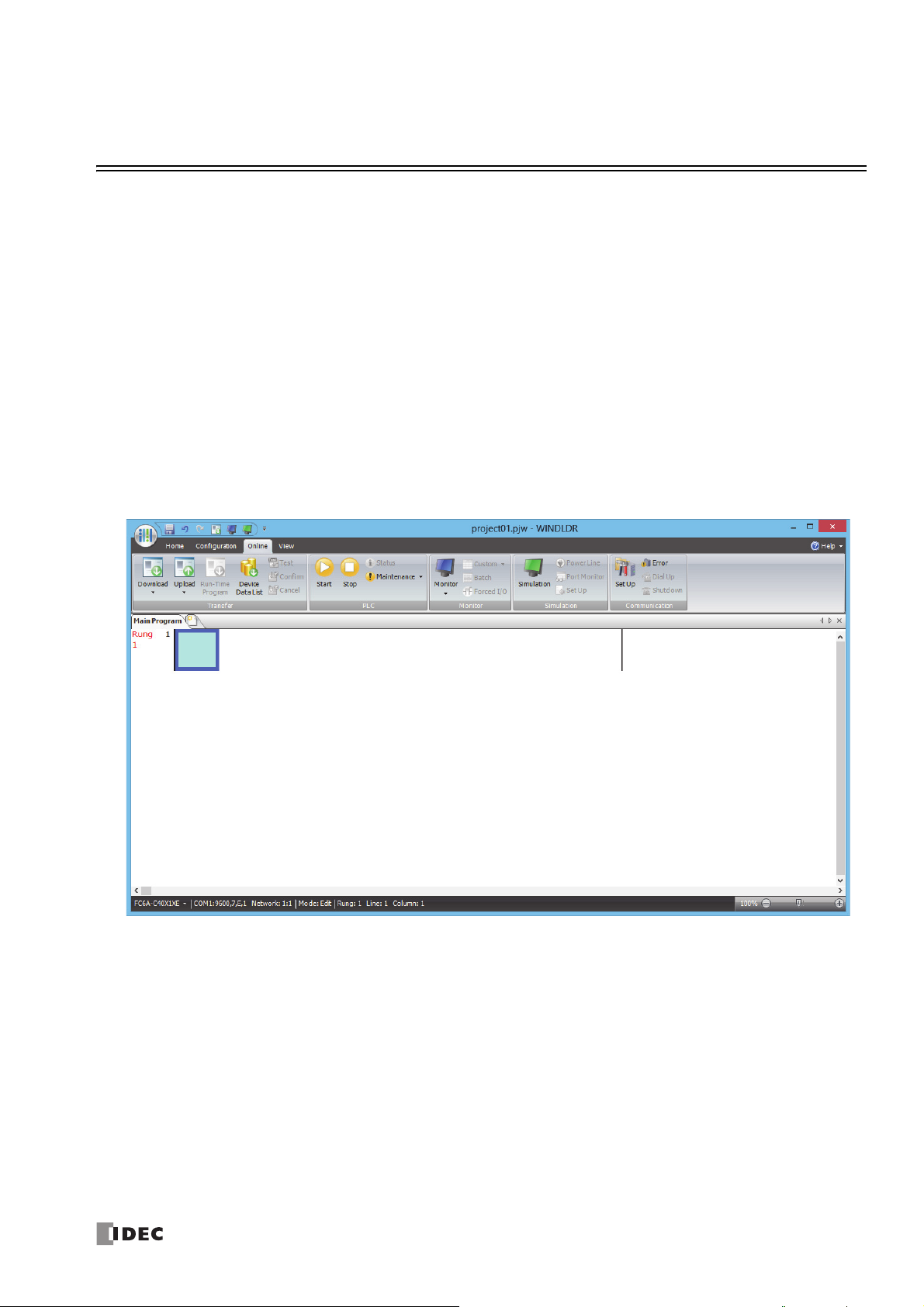
Start WindLDR
■ Windows 8
Click WindLDR in the tiles on the Start screen.
■ Windows 7, Windows Vista
Click Start and then Programs > Automation Organizer V2 > WindLDR > WindLDR.
■ Windows XP
From the Start menu of Windows, select Programs > Automation Organizer V2 > WindLDR > WindLDR.
WindLDR starts and a blank ladder editing screen appears with menus and tool bars shown on top of the screen.
FC6A S
ERIES MICROSMART
LAD P
ROGRAMMING MANUAL
FC9Y-B1726 1-1
Page 12
1: O
Select the PLC type from the list and click Use as
Default to set the selected PLC type as the default
type when WindLDR starts.
In WindLDR, the FC6A Series MicroSmart is categorized by the number of
inputs and outputs and the PLC type names are displayed as follows.
PLC Selection Option Type No.
FC6A-C16X1XE
FC6A-C16R1AE
FC6A-C16R1CE
FC6A-C16P1CE
FC6A-C16K1CE
FC6A-C24X1XE
FC6A-C24R1AE
FC6A-C24R1CE
FC6A-C24P1CE
FC6A-C24K1CE
FC6A-C40X1XE
FC6A-C40R1AE
FC6A-C40R1CE
FC6A-C40P1CE
FC6A-C40K1CE
FC6A-C40R1DE
FC6A-C40P1DE
FC6A-C40K1DE
FC6A-C40X1XEJ
FC6A-C40R1AEJ
FC6A-C40R1CEJ
FC6A-C40P1CEJ
FC6A-C40K1CEJ
FC6A-C40R1DEJ
FC6A-C40P1DEJ
FC6A-C40K1DEJ
PERATION BASICS
PLC Selection
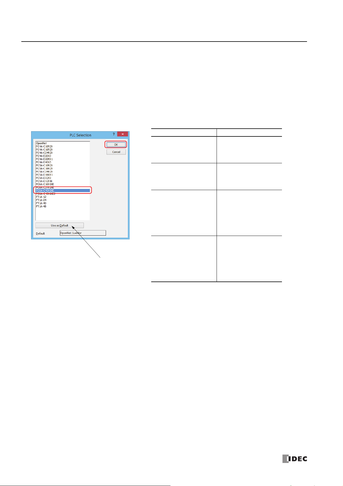
Before programming a user program on WindLDR, select a PLC type.
1. Select Configuration from the WindLDR menu bar, then select PLC Type.
The PLC Selection dialog box appears.
2. Select a PLC type in the selection box and the programming language to use.
3. Click OK.
PLC selection is now complete. Next, create a ladder program.
1-2 FC6A S
ERIES MICROSMART
LAD P
ROGRAMMING MANUAL
FC9Y-B1726
Page 13

1: O
PERATION BASICS
Create Program
Create Ladder Program
This section describes the operating procedure to create a ladder program in WindLDR.
Note: For details about devices, see "Devices" on page 2-1.
Sample User Program
Create a simple program using WindLDR. The sample program performs the following operation:
When only input I0 is turned on, output Q0 is turned on.
When only input I1 is turned on, output Q1 is turned on.
When both inputs I0 and I1 are turned on, output Q2 flashes in 1-s increments.
Rung No. Input I0 Input I1 Output Operation
1 ON OFF Output Q0 is turned ON.
2 OFF ON Output Q1 is turned ON.
3 ON ON Output Q2 flashes in 1-s increments.
Note: One collection of a group of instructions that control output or advanced instructions is called a rung. WindLDR manages programs in rung
units. Function descriptions can be configured as rung comments for individual rungs.
Start WindLDR
From the Start menu of Windows, select Programs > Automation Organizer V2 > WindLDR > WindLDR.
WindLDR starts and a blank ladder editing screen appears with menus and tool bars shown on top of the screen.
FC6A S
ERIES MICROSMART
LAD P
ROGRAMMING MANUAL
FC9Y-B1726 1-3
Page 14
1: O
PERATION BASICS
Edit User Program Rung by Rung
Start the user program with the LOD instruction by inserting a NO contact of input I0.
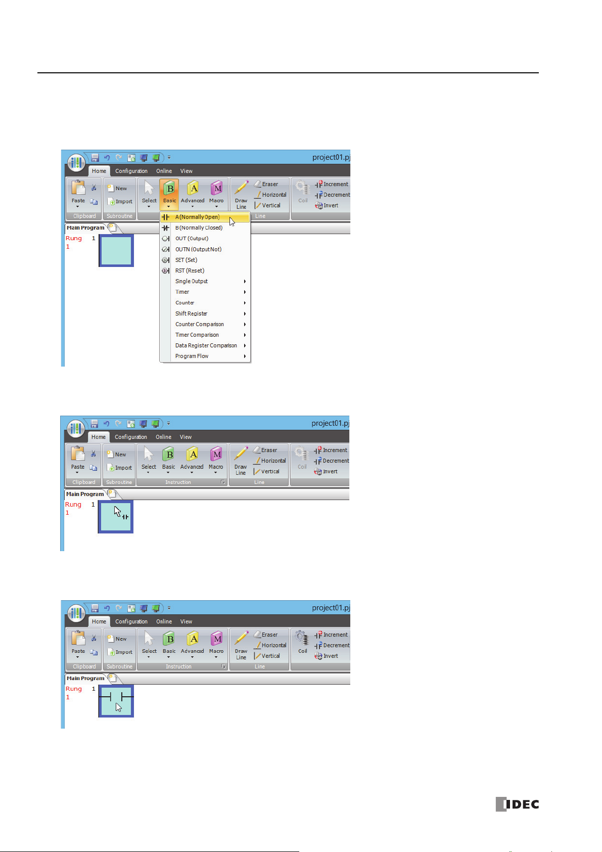
1. From the WindLDR menu bar, select Home > Basic > A (Normally Open).
2. Move the mouse pointer to the first column of the first line where you want to insert a NO contact, and click the left mouse
button.
3. Double-click Normally Open.
The A (Normally Open) dialog box is displayed.
1-4 FC6A S
ERIES MICROSMART
LAD P
ROGRAMMING MANUAL
FC9Y-B1726
Page 15
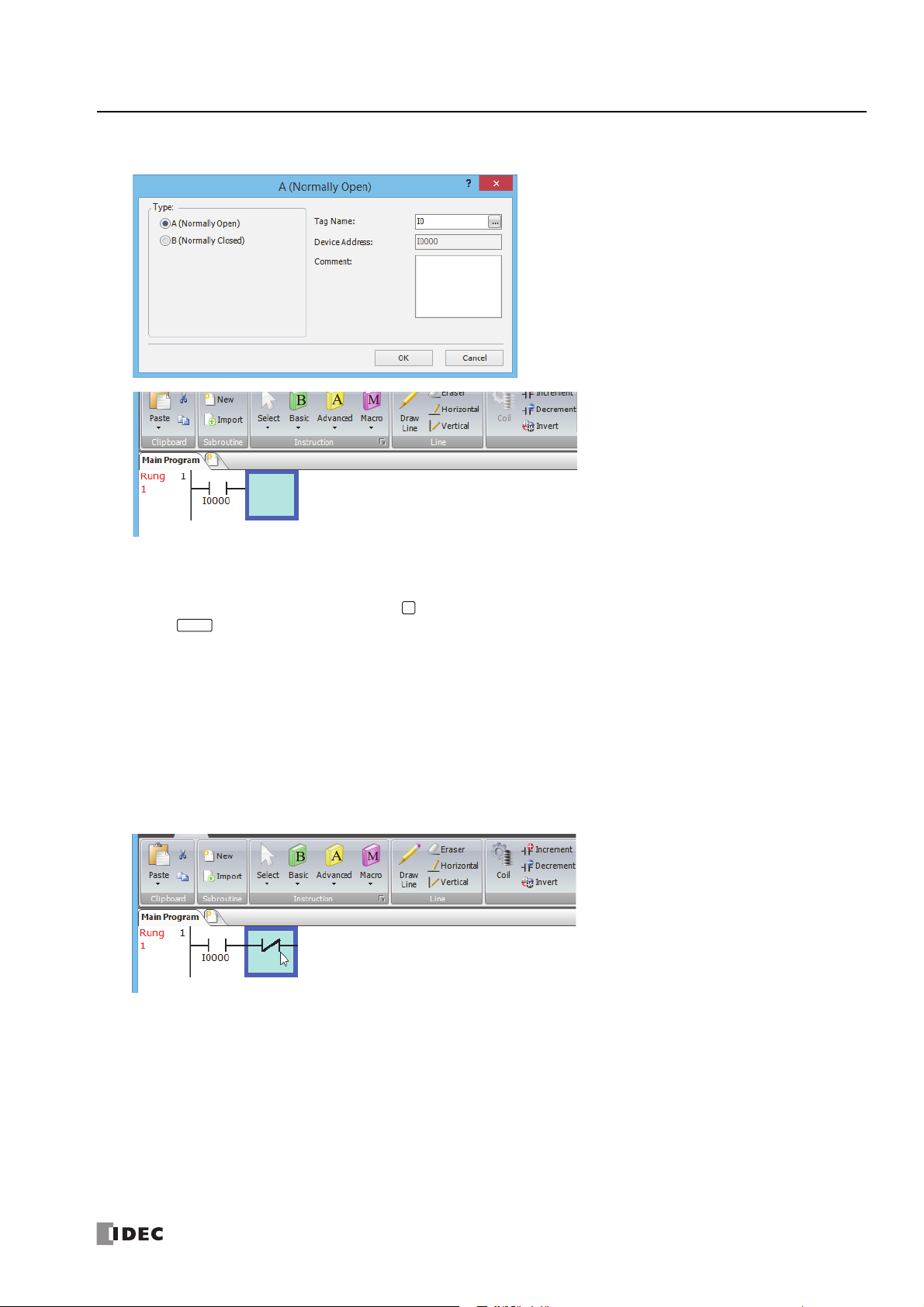
4. Enter I0 in the Tag Name field, and click OK.
A
Enter
1: O
PERATION BASICS
Note:
• To enter an NO contact from the right-click menu, right-click at the location to insert the NO contact, and on the right-click menu, click Basic
Instructions (B), then A (Normally Open).
• To enter an NO contact from the keyboard, press (A) to display the Coil Selection dialog box. Select A (Normally Open), and then
press (Enter).
A NO contact of input I0 is programmed in the first column of the first ladder line.
Next, program the ANDN instruction by inserting a NC contact of input I1.
5. From the WindLDR menu bar, select Home > Basic > B (Normally Closed).
6. Move the mouse pointer to the second column of the first ladder line where you want to insert a NC contact, and click the left
mouse button.
7. Double-click Normally Closed.
The B (Normally Closed) dialog box is displayed.
8. Enter I1 in the Tag Name field, and click OK.
An NC contact of input I1 is programmed in the second column of the first ladder line.
At the end of the first ladder line, program the OUT instruction by inserting a NO coil of output Q0.
9. From the WindLDR menu bar, select Home > Basic > OUT (Output).
10. Move the mouse pointer to the third column of the first ladder line where you want to insert an output coil, and click the left
mouse button.
Note: Another method to insert an instruction (either basic or advanced) is to type the instruction symbol, OUT, where you want to insert the
instruction.
FC6A S
ERIES MICROSMART
LAD P
ROGRAMMING MANUAL
FC9Y-B1726 1-5
Page 16
1: O
To insert a new ladder line
without creating a new rung,
press the down arrow key when
the cursor is on the last line or
press the right arrow key when
the cursor is at the right-most
column of the last line.
PERATION BASICS
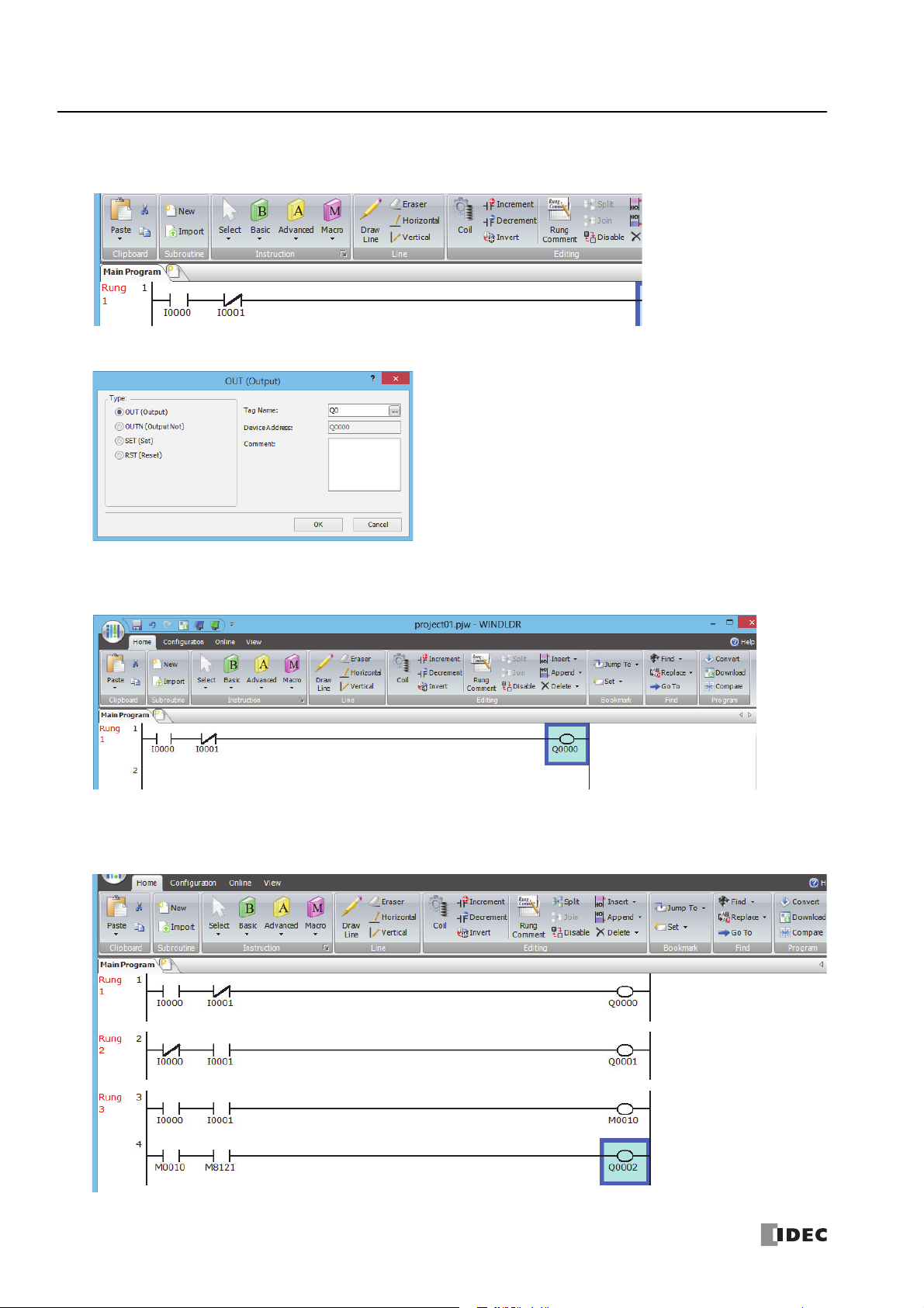
11. Double-click Output.
The Out (Output) dialog box is displayed.
12. Enter Q0 in the Tag Name field, and click OK.
A NO output coil of output Q0 is programmed in the right-most column of the first ladder line. This completes programming for
rung 1.
Continue programming for rungs 2 and 3 by repeating similar procedures.
A new rung is inserted by pressing the Enter key while the cursor is on the preceding rung. A new rung can also be inserted
by selecting Home > Append > Append a Rung.
When completed, the ladder program looks like below.
1-6 FC6A S
ERIES MICROSMART
LAD P
ROGRAMMING MANUAL
FC9Y-B1726
Page 17
1: O
Info Window
PERATION BASICS
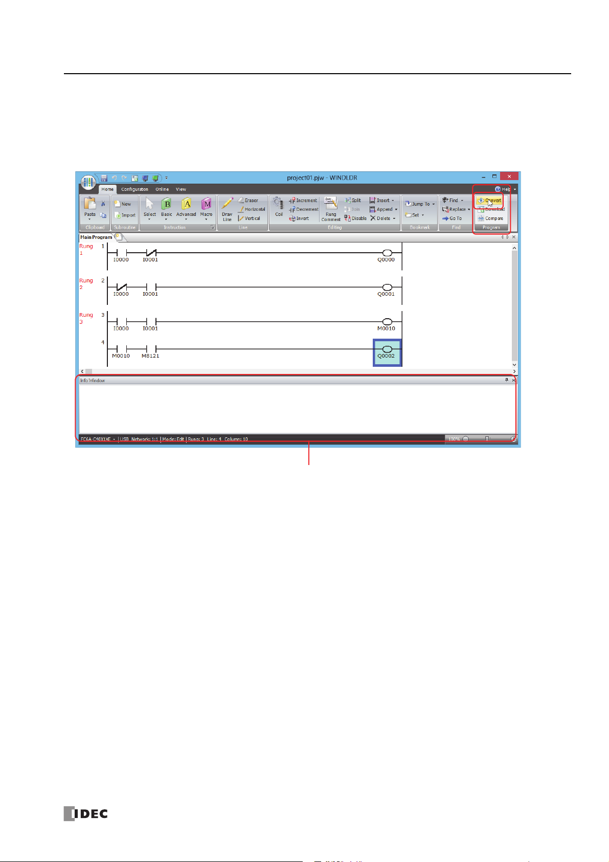
Convert Program
The program can be checked whether it contains any user program syntax error.
From the menu bar, select Home > Convert (Program group).
When the instruction/FB symbols are connected correctly, the program conversion is completed successfully. If any error is found,
the errors are listed on the Info Window. Then, make corrections as necessary.
FC6A S
ERIES MICROSMART
LAD P
ROGRAMMING MANUAL
FC9Y-B1726 1-7
Page 18
1: O
PERATION BASICS
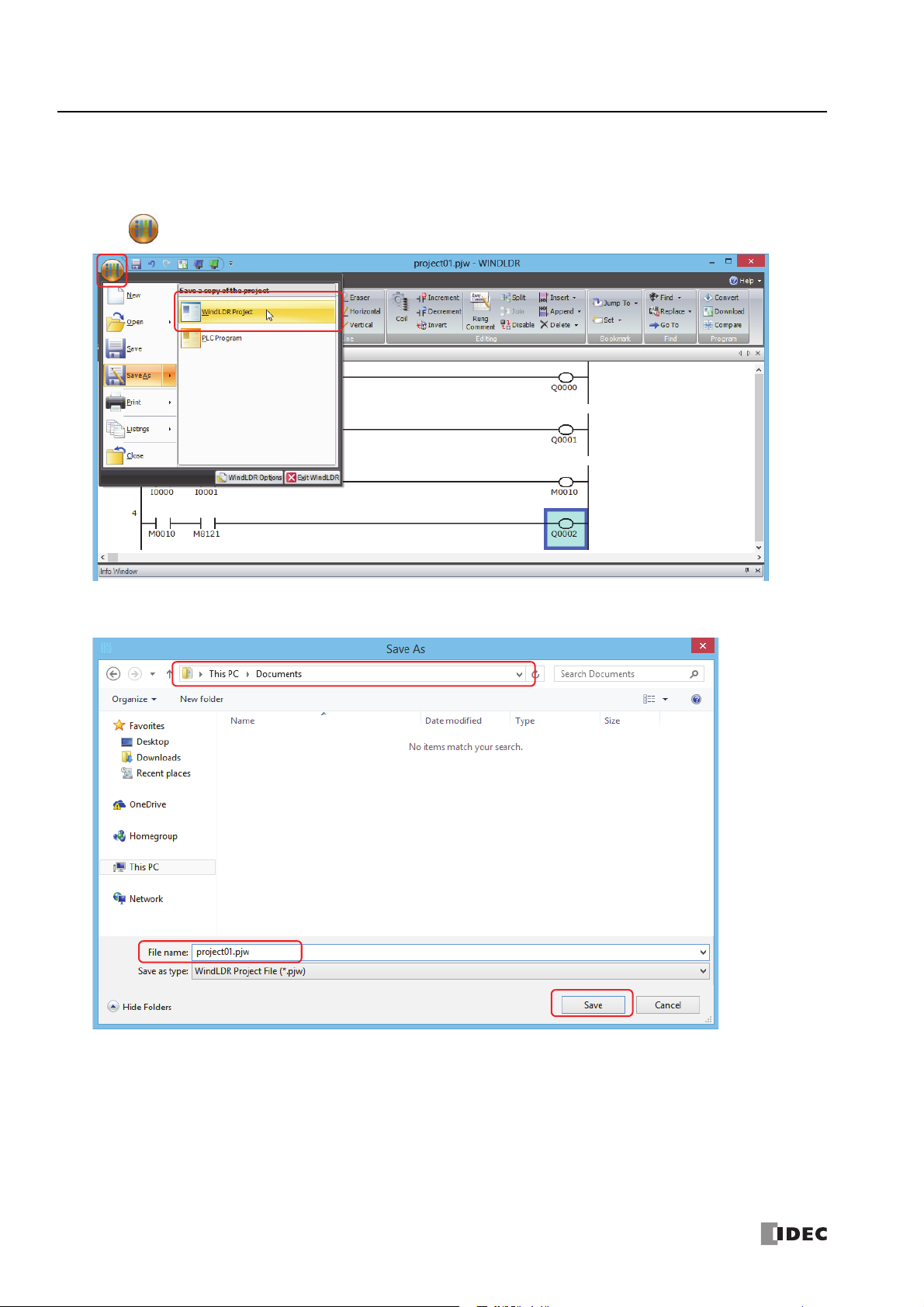
Save Project
This section describes the operating procedure to save the created ladder program as a project file.
1. Save the current project with a new name.
Click
2. Enter the file name in File name, specify the folder to save to, and click Save.
(application) button > Save As > WindLDR Project.
This completes the procedure to save a project to a file.
Note: The saved file is called a project file. The extension is ".pjw".
1-8 FC6A S
ERIES MICROSMART
LAD P
ROGRAMMING MANUAL
FC9Y-B1726
Page 19
1: O
PERATION BASICS
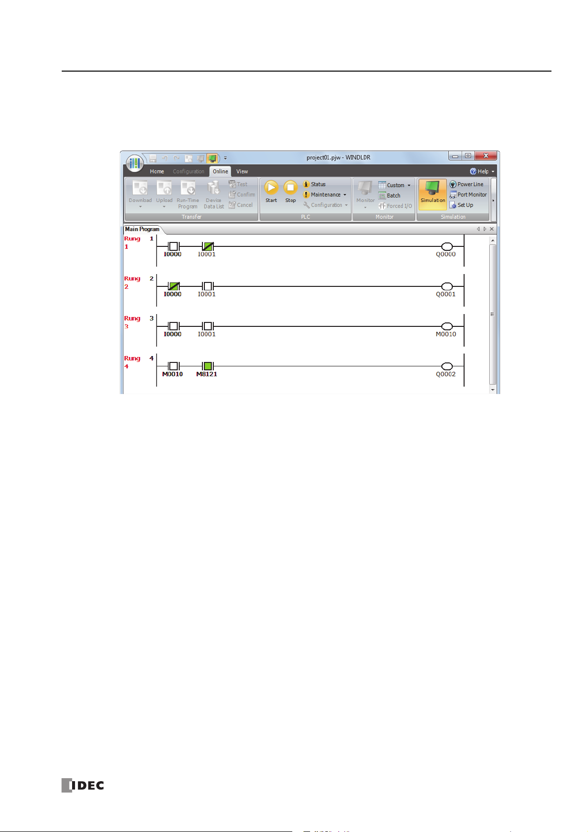
Simulate Operation
This section describes the operating procedure to check the operation of the user program before transferring it to the FC6A Series
MicroSmart.
From the WindLDR menu bar, select Online > Simulation. The Simulation screen appears.
Select and right-click the input contact you want to change, and on the right-click menu, click Set or Reset.
To quit simulation, from the WindLDR menu bar, select Online > Simulation.
Notes:
• You can also change the status of an input contact by double-clicking it.
• To quit simulation, from the WindLDR menu bar, once more select Online > Simulation > Simulation.
FC6A S
ERIES MICROSMART
LAD P
ROGRAMMING MANUAL
FC9Y-B1726 1-9
Page 20
1: O
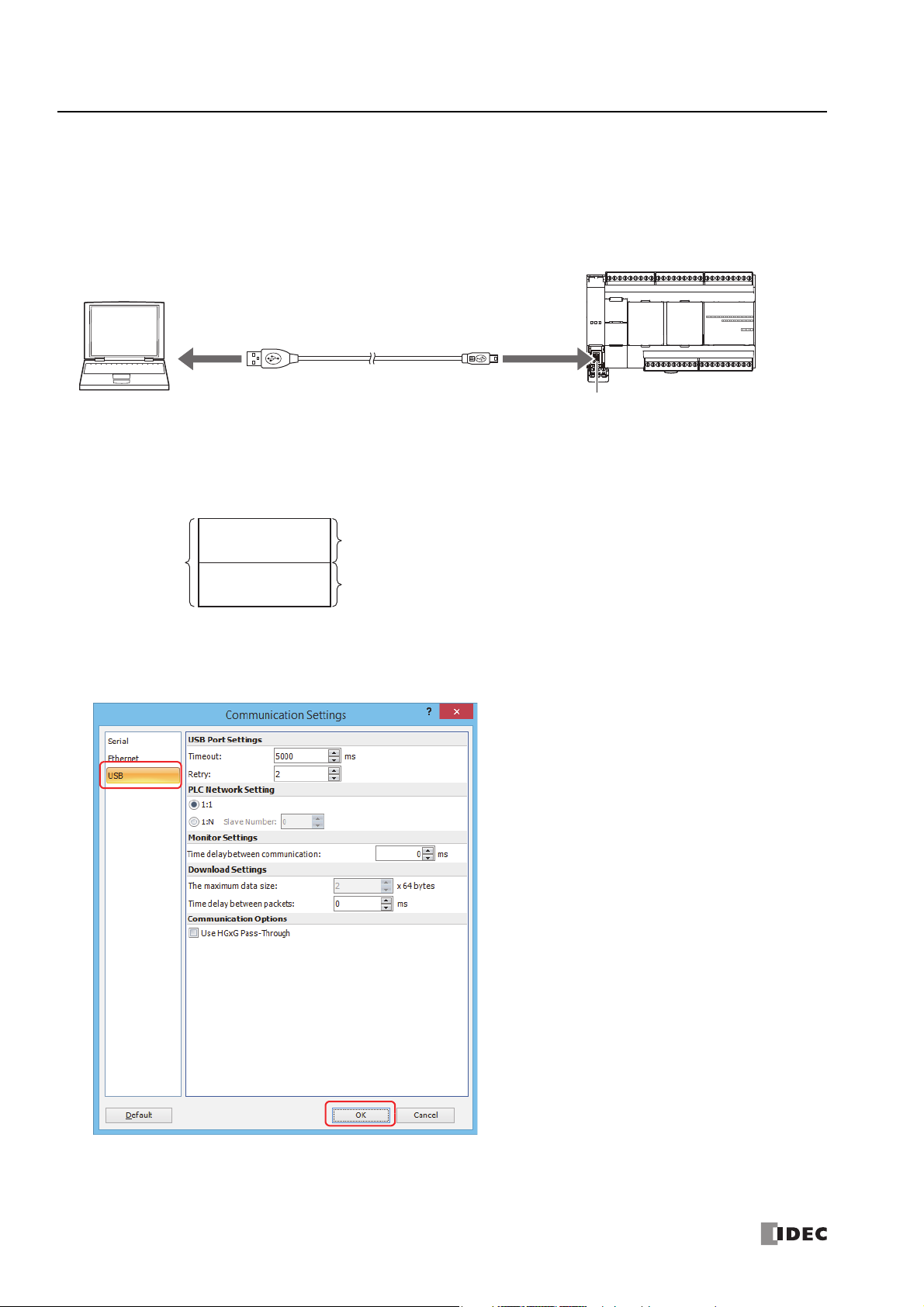
Windows Computer
USB Port
USB Cable
HG9Z-XCM42 USB Maintenance Cable
FC6A Series MicroSmart
Type A Plug Mini-B Plug
USB Port
(USB 2.0 Mini-B Connector)
Ladder Program
Function Area Settings
User Program
Details programmed with a ladder diagram
Details of the FC6A Series MicroSmart settings
The majority of these items are those set on the Configuration tab.
PERATION BASICS
Download Program
While WindLDR is running on a PLC, you can download the user program to the FC6A Series MicroSmart.
User programs can be downloaded to the FC6A Series MicroSmart from WindLDR using USB or Ethernet.
This section describes the operating procedure from configuring communication settings to downloading the user program using a
USB connection as an example.
Notes:
• In order for WindLDR to communicate with the FC6A Series MicroSmart via USB, a dedicated USB driver must be installed on the computer.
See Appendix "USB Driver Installation Procedure" in the "FC6A Series MicroSmart All-in-One Type User’s Manual".
• A user program is a combination of a ladder program and the setting details (Function Area Settings).
1. From the WindLDR menu bar, select Online > Set Up.
The Communication Settings dialog box is displayed.
2. Click the USB tab and then click OK.
1-10 FC6A S
The communication method is now set to USB. Next, download a user program.
ERIES MICROSMART
LAD P
ROGRAMMING MANUAL
FC9Y-B1726
Page 21
1: O
PERATION BASICS
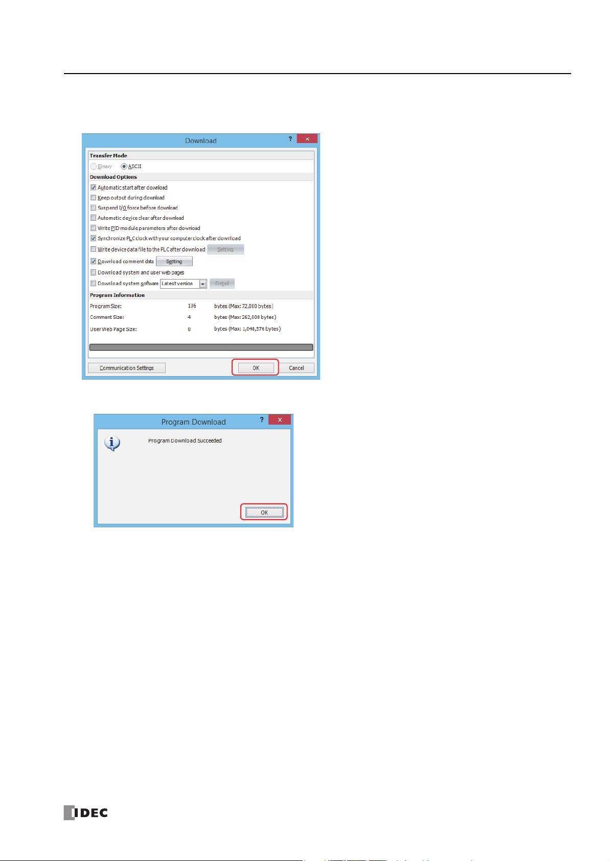
3. From the WindLDR menu bar, select Online > Download. The Download dialog box appears, then click OK. The user
program is downloaded to the FC6A Series MicroSmart.
Note: The Download dialog box can also be opened by
selecting Home > Download.
Note: When downloading a user program, all values and
selections in the Function Area Settings are also
downloaded to the FC6A Series MicroSmart. For details on
function settings, see Chapter 5 "Functions and Settings" in
the "FC6A Series MicroSmart All-in-One Type User’s Manual".
When the following message appears, the download has completed successfully. Click OK.
FC6A S
ERIES MICROSMART
LAD P
ROGRAMMING MANUAL
FC9Y-B1726 1-11
Page 22
1: O
Rung 1:
When both inputs I0 and I1 are on,
output Q0 is turned off.
Rung 2:
When both inputs I0 and I1 are on,
output Q1 is turned off.
Rung 3:
When both input I0 and I1 are on,
internal relay M10 is turned on.
M8121 is the 1-s clock special
internal relay.
While M10 is on, output Q2 flashes
in 1-s increments.
PERATION BASICS
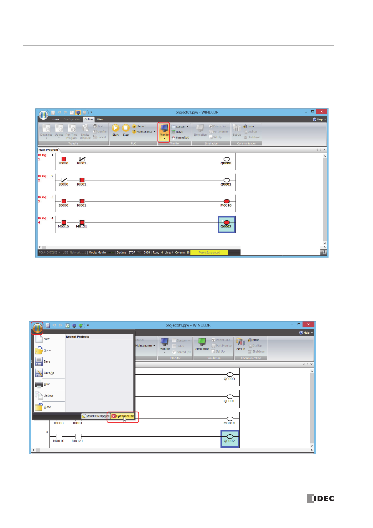
Monitor Operation
Another powerful function of WindLDR is to monitor the PLC operation on the computer. The input and output statuses of the
sample program can be monitored in the ladder diagram.
From the WindLDR menu bar, select Online > Monitor > Monitor.
When both inputs I0 and I1 are on, the ladder diagram on the monitor screen looks as follows:
Exit WindLDR
This section describes the operating procedure to exit WindLDR.
When you have completed monitoring, you can exit WindLDR either directly from the monitor screen or from the editing screen. In
both cases, from the WindLDR application button, click Exit WindLDR.
1-12 FC6A S
ERIES MICROSMART
LAD P
ROGRAMMING MANUAL
FC9Y-B1726
Page 23
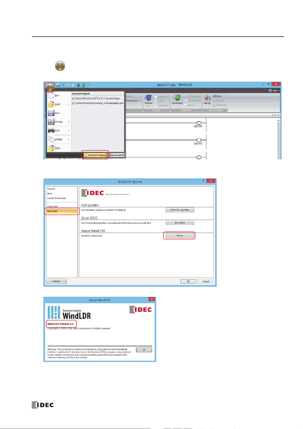
Checking the WindLDR Version Number
This section describes how to check the WindLDR version.
1. Click (application) button > WindLDR Options.
The WindLDR Options dialog box appears.
2. Click the Resources tab, and then click About.
The About WindLDR dialog box appears.
1: O
PERATION BASICS
You can check the WindLDR version. When finished, click OK.
Note: When using the FC6A Series MicroSmart, use version 8.0.0 or later of WindLDR.
If you are using a version of WindLDR that does not meet this condition, click Check for Updates on the Resources tab to obtain the latest
version of WindLDR.
This concludes the procedure for checking the WindLDR version.
FC6A S
ERIES MICROSMART
LAD P
ROGRAMMING MANUAL
FC9Y-B1726 1-13
Page 24
1: O
Input Refresh
Input Terminals
Input Device
Output Device
Ladder Processing
Output Refresh
Other Processing
Output Terminals
Input CircuitOutput Circuit
I0: ON
I1: OFF
I2: ON
Q0: ON
Q1: OFF
Q2: ON
0: ON
1: OFF
2: ON
0: ON
1: OFF
2: ON
Repeat operations
One sequence of operations is set as one
scan, and the time required is set as the
scan time.
The output devices are updated
according to the ladder program.
The input device values are applied to the
ladder program.
Processing other than the ladder
processing is called the END
processing.
The ON/OFF status of the input terminal
(external input) is applied to the input
circuit. The input refresh loads the external
input status into the input devices (I) by
way of the input circuit.
A delay occurs until the ON/OFF status of
the input circuit is applied to the input
devices (I). The delay time is equal to filter
time + 1 scan time.
The output refresh applies the status of the
output devices (Q) to the output circuit, and
then the ON/OFF status of the output
terminals (external input) is updated.
A delay occurs until the values of the output
devices (Q) are applied to the output circuit.
The delay time is at maximum 1 scan time.
PERATION BASICS
Ladder Program Operation
The FC6A Series MicroSmart performs the following operations to process ladder programs.
Notes:
• The delay time of the hardware is added to the actual input and output delay times.
For details on the hardware input/output delay times, see Chapter 2 "Product Specifications" in the "FC6A Series MicroSmart All-in-One Type
User’s Manual".
• The filter time differs depending on the input used.
• When the input is a CPU module input (I0 to I27)
See the input filter time configured in the WindLDR Function Area Settings. The initial value is 3 ms.
• When the input is an expansion input (I30 or greater)
There is no filter time.
1-14 FC6A S
ERIES MICROSMART
LAD P
ROGRAMMING MANUAL
FC9Y-B1726
Page 25

1: O
Caution
PERATION BASICS
Start/Stop Operation
This section describes how to run and stop the FC6A Series MicroSmart.
Make sure of safety before starting and stopping the FC6A Series MicroSmart. Incorrect operation of the FC6A Series
MicroSmart may cause machine damage or accidents.
Start/Stop Schematic
You can start and stop FC6A Series MicroSmart operations by using WindLDR operations, FC6A Series MicroSmart operations,
function switch operations, menu operations using an HMI module, by turning the FC6A Series MicroSmart on or off, or by using
the stop/reset input function by way of external input.
• For operations using WindLDR, see "Start/Stop Operation Using WindLDR" on page 1-15.
• For operations using the FC6A Series MicroSmart power supply, see "Start/Stop Operation Using the Power Supply" on page
1-16.
• For operations using the function switch, see Chapter 5 "Function Switch Configuration" in the "FC6A Series MicroSmart All-inOne Type User’s Manual".
• For operations using an HMI module, see Chapter 7 "HMI Function" in the "FC6A Series MicroSmart All-in-One Type User’s
Manual".
• For the stop input settings, see Chapter 5 "Stop Input" in the "FC6A Series MicroSmart All-in-One Type User’s Manual".
• For the reset input settings, see Chapter 5 "Reset Input" in the "FC6A Series MicroSmart All-in-One Type User’s Manual".
The switch from start to stop is performed during the END processing of the user program, and the following functions are also
stopped when the user program is stopped. For details on END processing, see the "Breakdown of END Processing Time" on page
A-5.
High-speed counter/frequency measurement/user interrupt/catch input/timer interrupt/user communication/pulse output
• You can use M8025 (Maintain Outputs While Stopped) to select whether to maintain or clear the outputs while the CPU is
stopped.
For details on M8025 (Maintain Outputs While Stopped), see "M8025: Maintain Outputs While Stopped" on page 2-8.
• The current value of the timer instruction is reset.
For details on timer instructions, see "TML (1-s Timer)" on page 4-7".
Also, when you switch from stop to start, the device status is cleared or kept depending on Memory Backup in the Function
Area Settings. For details, see Chapter 5 "Memory Backup" in the "FC6A Series MicroSmart All-in-One Type User’s Manual".
Start/Stop Operation Using WindLDR
The FC6A Series MicroSmart can be started and stopped using WindLDR run on a Windows computer connected to the FC6A
Series MicroSmart. When the
turned on to start the FC6A Series MicroSmart. When the
MicroSmart.
1. Connect the computer to the FC6A Series MicroSmart, start WindLDR, and power up the FC6A Series MicroSmart.
2. Check that a stop input is not designated using Configuration > Run/Stop Control > Stop and Reset Inputs. See
Chapter 5 "Stop Input and Reset Input" in the "FC6A Series MicroSmart All-in-One Type User’s Manual".
Note: When a stop input is designated, the FC6A Series MicroSmart cannot be started or stopped by turning start control special internal relay
M8000 on or off.
3. Select Online from the WindLDR menu bar.
The Online tab appears.
4. Click the Start button to start operation, then the start control special internal relay M8000 is turned on.
Start button is pressed in the menu bar shown below, start control special internal relay M8000 is
Stop button is pressed, M8000 is turned off to stop the FC6A Series
FC6A S
ERIES MICROSMART
LAD P
ROGRAMMING MANUAL
FC9Y-B1726 1-15
Page 26

1: O
PERATION BASICS
5. Click the Stop button to stop operation, then the start control special internal relay M8000 is turned off.
The PLC operation can also be started and stopped while WindLDR is in the monitor mode. Select Online
> Monitor >
Monitor and click the Start or Stop button.
Note: Special internal relay M8000 is a keep type internal relay and stores the status when power is turned off. M8000 retains its previous status
when power is turned on again. However, when the backup battery is dead, M8000 loses the stored status, and can be turned on or off as
programmed when the FC6A Series MicroSmart is powered up. The selection is made in Configuration > Run/Stop Control > Run/Stop
Selection at Memory Backup Error. See Chapter 5 "Run/Stop Selection at Keep Data Error" in the "FC6A Series MicroSmart All-in-One Type
User’s Manual".
The backup duration is approximately 30 days (typical) at 25°C after the backup battery is fully charged.
Start/Stop Operation Using the Power Supply
The FC6A Series MicroSmart can be started and stopped by turning power on and off.
1. Power up the FC6A Series MicroSmart to start operation.
2. Turn power on and off to start and stop operation.
1-16 FC6A S
ERIES MICROSMART
LAD P
ROGRAMMING MANUAL
FC9Y-B1726
Page 27

2: D
EVICES
This chapter provides detailed descriptions of the allocations of devices such as inputs, outputs, internal relays, registers, timers,
and counters that are used in the basic and advanced instructions, as well as details about the allocations of special internal relays
and special data registers.
Please use this chapter as a reference for the devices.
Note: The entry and operation of FC6A Series MicroSmart user programs requires specialist knowledge.
Take the time to develop a thorough understanding of the contents and programs in this manual before using the FC6A Series MicroSmart.
Device Addresses
Device Symbol Unit
*1
Inputs
Expansion Input Relays
*1
Output
Expansion Outputs
Internal Relay
Special Internal Relay
Shift Register R Bit
Timer T Bit/Word
Counter C Bit/Word
Data Register D Bit/Word
Special Data Register D Bit/Word
*1 The least significant digit of the device address is an octal number (0 to 7).
*2 I190 to I507 and Q190 to Q507 are devices that can only be used when an expansion module (expansion interface side) is connected using the
expansion interface module.
*3 I310 to I627 and Q310 to Q627 are devices that can only be used when an expansion module (expansion interface side) is connected using the
expansion interface module.
*1
*1
*1*3
*1
IBit
IBit
QBit
QBit
MBit
MBit
16-I/O Type 24-I/O Type 40-I/O Type
I0 - I10
(9 points)
I30 - I187
(128 points)
I190 - I507
(256 points)
(7 points)
Q30 - Q187
(128 points)
Q190 - Q507
(256 points)
*2
Q0 - Q6
*2
Range (Points)
I0 - I15
(14 points)
(224 points)
I310 - I627
(256 points)
Q0 - Q11
(10 points)
Q30 - Q307
(224 points)
Q310 - Q627
(256 points)
M0 - M7997
(6,400 points)
M10000 - M17497
(6,000 points)
M8000 - M8317
(256 points)
R0 - R255
(256 points)
T0 - T1023
(1,024 points)
C0 - C511
(512 points)
D0000 - D7999
(8,000 points)
D10000 to D55999
(46,000 points)
D8000 - D8499
(500 points)
I0 - I27
(24 points)
I30 - I307
*3
Q0 - Q17
(16 points)
*3
FC6A S
ERIES MICROSMART
LAD P
ROGRAMMING MANUAL
FC9Y-B1726 2-1
Page 28

2: D
EVICES
■ Inputs (I), Expansion Inputs (I)
Devices that input on/off information from external devices to the FC6A Series MicroSmart.
■ Outputs (Q), Expansion Outputs (Q)
Devices that output on/off information from the FC6A Series MicroSmart to external devices.
■ Internal Relays (M)
Bit devices used internally on the FC6A Series MicroSmart.
■ Special Internal Relays (M)
Bit devices used internally on the FC6A Series MicroSmart. Special functions are assigned to each bit.
■ Shift Registers (R)
Bit devices that are used with the SFR instruction and the SFRN instruction. The bit sequence of the data is shifted according to
pulse input.
■ Timer (T)
Timers used internally in the FC6A Series MicroSmart. There are three devices: Timer bits (symbol: T, unit: bit), timer preset
values (symbol: TP, unit: word), and timer current values (symbol: TC, unit: word).
These can be used as an on-delay timer or an off-delay timer. For details on timers (T), see "Using Timer or Counter as Source
Device" on page 3-6.
■ Counters (C)
Counters used internally in the FC6A Series MicroSmart. There are three devices: Counter bits (symbol: C, unit: bit), counter
preset values (symbol: CP, unit: word), and counter current values (symbol: CC, unit: word). These can be used as an adding
counter or a reversible counter. For details on counters (C), see "Using Timer or Counter as Source Device" on page 3-6.
■ Data Registers (D)
Word devices that are used for writing numerical data internally in the FC6A Series MicroSmart. These can also be used as bit
devices.
■ Special Data Registers (D)
Word devices that are used for writing numerical data internally in the FC6A Series MicroSmart. Special functions are assigned to
each data register. These can also be used as bit devices.
Notes:
• Although the device symbol for internal relays (M0000 to M7997, M10000 to M17497) and special internal relays (M8000 to M8317) is the
same ("M"), the device characteristics are different. Special functions are assigned to each bit of the special internal relays.
• Although the device symbol for the data registers (D0000 to D7999, D10000 to D55999) and special data registers (D8000 to D8499) is the
same ("D"), the device characteristics are different. Special functions are assigned to each special data register.
2-2 FC6A S
ERIES MICROSMART
LAD P
ROGRAMMING MANUAL
FC9Y-B1726
Page 29
Special Internal Relay
Warning
Special Internal Relay Device Addresses
Do not write to data in the area marked as reserved in the special internal relays list. Otherwise the system may not operate
correctly.
Note: R/W is an abbreviation for read/write.
The notation for the R/W field is as follows.
R/W: The device can be both read from and written to
R: Read-only
W: Write-only
2: D
EVICES
Device
Address
M8000 Start Control Maintained Maintained R/W
M8001 1-s Clock Reset Cleared Cleared R/W
M8002 All Outputs OFF Cleared Cleared R/W
M8003 Carry (Cy) or Borrow (Bw) Cleared Cleared R/W
M8004 User Program Execution Error Cleared Cleared R/W
M8005 Communication Error Maintained Cleared R/W
M8006 Communication Prohibited Flag (When Data Link Master) Maintained Maintained R/W
M8007
M8010 Status LED Operation Operating Cleared R/W
M8011
M8012
M8013 Calendar/Clock Data Write/Adjust Error Flag Operating Cleared R/W
M8014 Calendar/Clock Data Read Error Flag Operating Cleared R/W
M8015 — Reserved — — — —
M8016 Calendar Data Write Flag Operating Cleared R/W
M8017 Clock Data Write Flag Operating Cleared R/W
M8020 Calendar/Clock Data Write Flag Operating Cleared R/W
M8021 Clock Data Adjust Flag Operating Cleared R/W
M8022 User Communication Receive Instruction Cancel Flag (Port 1) Cleared Cleared R/W
M8023 User Communication Receive Instruction Cancel Flag (Port 2) Cleared Cleared R/W
M8024 BMOV/WSFT Executing Flag Maintained Maintained R/W
M8025 Maintain Outputs While Stopped Maintained Cleared R/W
M8026 User Communication Receive Instruction Cancel Flag (Port 3) Cleared Cleared R/W
M8027
M8030 Comparison Output Reset Cleared Cleared R/W
M8031 Gate Input Maintained Cleared R/W
M8032 Reset Input Maintained Cleared R/W
M8033 — Reserved — — — —
M8034
M8035 Gate Input Maintained Cleared R/W
M8036 Reset Input Maintained Cleared R/W
M8037 — Reserved — — — —
M8040
M8041 Gate Input Maintained Cleared R/W
M8042 Reset Input Maintained Cleared R/W
M8043
M8044 Comparison Output Reset Maintained Cleared R/W
M8045 Gate Input Maintained Cleared R/W
M8046 Reset Input Maintained Cleared R/W
M8047
M8050
Initialization Flag (When Data Link Master)/Stop Communication Flag (When
Data Link Slave)
— Reserved — — — —
High-speed Counter (Group 1/I0)
High-speed Counter (Group 3/I3)
High-speed Counter (Group 4/I4)
High-speed Counter (Group 5/I6)
— Reserved — — — —
Description
Count Direction Flag Maintained Cleared R/W
Comparison Output Reset Cleared Cleared R/W
Comparison Output Reset Cleared Cleared R/W
Count Direction Flag Cleared Cleared R/W
When
Stopped
Cleared Cleared R/W
Power
OFF
R/W
FC6A S
ERIES MICROSMART
LAD P
ROGRAMMING MANUAL
FC9Y-B1726 2-3
Page 30

2: D
EVICES
Device
Address
M8051
M8052 Gate Input Maintained Cleared R/W
M8053 Reset Input Maintained Cleared R/W
M8054 Comparison ON Status Maintained Cleared R
M8055 Overflow Maintained Cleared R
M8056 — Reserved — — — —
M8057
M8060 Gate Input Maintained Cleared R/W
M8061 Reset Input Maintained Cleared R/W
M8062 Comparison ON Status Maintained Cleared R
M8063 Overflow Maintained Cleared R
M8064 to
M8067
M8070 SD Memory Card Mount Status Maintained Cleared R
M8071 Accessing SD Memory Card Maintained Cleared R
M8072 Unmount SD Memory Card Operating Cleared R/W
M8073 Function Switch Status Operating Cleared R
M8074 Battery Voltage Measurement Flag Operating Cleared R/W
M8075 to
M8077
M8080 Data Link Slave 1 Communication Completed Relay (When Data Link Master) Operating Cleared R
M8081 Data Link Slave 2 Communication Completed Relay Operating Cleared R
M8082 Data Link Slave 3 Communication Completed Relay Operating Cleared R
M8083 Data Link Slave 4 Communication Completed Relay Operating Cleared R
M8084 Data Link Slave 5 Communication Completed Relay Operating Cleared R
M8085 Data Link Slave 6 Communication Completed Relay Operating Cleared R
M8086 Data Link Slave 7 Communication Completed Relay Operating Cleared R
M8087 Data Link Slave 8 Communication Completed Relay Operating Cleared R
M8090 Data Link Slave 9 Communication Completed Relay Operating Cleared R
M8091 Data Link Slave 10 Communication Completed Relay Operating Cleared R
M8092 Data Link Slave 11 Communication Completed Relay Operating Cleared R
M8093 Data Link Slave 12 Communication Completed Relay Operating Cleared R
M8094 Data Link Slave 13 Communication Completed Relay Operating Cleared R
M8095 Data Link Slave 14 Communication Completed Relay Operating Cleared R
M8096 Data Link Slave 15 Communication Completed Relay Operating Cleared R
M8097 Data Link Slave 16 Communication Completed Relay Operating Cleared R
M8100 Data Link Slave 17 Communication Completed Relay Operating Cleared R
M8101 Data Link Slave 18 Communication Completed Relay Operating Cleared R
M8102 Data Link Slave 19 Communication Completed Relay Operating Cleared R
M8103 Data Link Slave 20 Communication Completed Relay Operating Cleared R
M8104 Data Link Slave 21 Communication Completed Relay Operating Cleared R
M8105 Data Link Slave 22 Communication Completed Relay Operating Cleared R
M8106 Data Link Slave 23 Communication Completed Relay Operating Cleared R
M8107 Data Link Slave 24 Communication Completed Relay Operating Cleared R
M8110 Data Link Slave 25 Communication Completed Relay Operating Cleared R
M8111 Data Link Slave 26 Communication Completed Relay Operating Cleared R
M8112 Data Link Slave 27 Communication Completed Relay Operating Cleared R
M8113 Data Link Slave 28 Communication Completed Relay Operating Cleared R
M8114 Data Link Slave 29 Communication Completed Relay Operating Cleared R
M8115 Data Link Slave 30 Communication Completed Relay Operating Cleared R
M8116 Data Link Slave 31 Communication Completed Relay Operating Cleared R
M8117 Data Link All Slaves Communication Completed Relay Operating Cleared R
M8120 Initialize Pulse Cleared Cleared R
M8121 1-s Clock Operating Cleared R
M8122 100-ms Clock Operating Cleared R
High-speed Counter (Group 2/I1)
High-speed Counter (Group 6/I7)
— Reserved — — — —
— Reserved — — — —
Description
Comparison Output Reset Cleared Cleared R/W
Comparison Output Reset Cleared Cleared R/W
When
Stopped
Power
OFF
R/W
2-4 FC6A S
ERIES MICROSMART
LAD P
ROGRAMMING MANUAL
FC9Y-B1726
Page 31

2: D
EVICES
Device
Address
M8123 10-ms Clock Operating Cleared R
M8124 Timer/Counter Preset Value Changed Maintained Cleared R
M8125 In-operation Output Cleared Cleared R
M8126 1 Scan ON After Run-Time Download Completes Cleared Cleared R
M8127 — Reserved — — — —
M8130
M8131 Comparison ON Status Maintained Cleared R
M8132 — Reserved — — — —
M8133 High-speed Counter (Group 3/I3) Comparison ON Status Maintained Cleared R
M8134 High-speed Counter (Group 4/I4) Comparison ON Status Maintained Cleared R
M8135
M8136 Comparison ON Status Maintained Cleared R
M8137 Interrupt Input I0 Status (Group 1/I0)
M8140 Interrupt Input I1 Status (Group 2/I1) Cleared Cleared R
M8141 Interrupt Input I3 Status (Group 3/I3) Cleared Cleared R
M8142 Interrupt Input I4 Status (Group 4/I4) Cleared Cleared R
M8143 Interrupt Input I6 Status (Group 5/I6) Cleared Cleared R
M8144 Timer Interrupt Status Cleared Cleared R
M8145 to
M8147
M8150 Comparison Result 1 Maintained Cleared R
M8151 Comparison Result 2 Maintained Cleared R
M8152 Comparison Result 3 Maintained Cleared R
M8153
M8154 Group 2/I1 Maintained Cleared R
M8155 Group 3/I3 Maintained Cleared R
M8156 Group 4/I4 Maintained Cleared R
M8157 Group 5/I6 Maintained Cleared R
M8160 Group 6/I7 Maintained Cleared R
M8161
M8162 Underflow Maintained Cleared R
M8163
M8164 Underflow Maintained Cleared R
M8165 High-speed Counter (Group 3/I3) Overflow Maintained Cleared R
M8166 High-speed Counter (Group 4/I4) Overflow Maintained Cleared R
M8167 Interrupt Input I7 Status (Group 6/I7) (ON: Allowed, OFF: Prohibited) Maintained Cleared R
M8170
M8171
M8172
M8173 Group 2 Operating Cleared R
M8174 Group 3 Operating Cleared R
M8175 Group 4 Operating Cleared R
M8176 to
M8183
M8184 Change HMI Module Network Settings Trigger Operating Cleared R/W
M8185 In Daylight Saving Time Period Operating Cleared R
M8186 Executing Auto Ping Operating Cleared R
M8187 Auto Ping Stop Flag Operating Cleared R/W
M8190 Change CPU Module Network Settings Trigger Operating Cleared R/W
M8191 SNTP Acquisition Flag Operating Cleared R/W
High-speed Counter (Group 1/I0)
High-speed Counter (Group 5/I6)
— Reserved — — — —
Catch Input ON/OFF Status
High-speed Counter (Group 1/I0)
High-speed Counter (Group 5/I6)
— Reserved — — — —
Transistor Source Output Overcurrent
Detection
— Reserved — — — —
Description
Reset Status Maintained Cleared R
Reset Status Maintained Cleared R
(ON: Allowed, OFF: Prohibited)
Group 1/I0 Maintained Cleared R
Overflow Maintained Cleared R
Overflow Maintained Cleared R
Group 1 Operating Cleared R
When
Stopped
Cleared Cleared R
Power
OFF
R/W
FC6A S
ERIES MICROSMART
LAD P
ROGRAMMING MANUAL
FC9Y-B1726 2-5
Page 32

2: D
EVICES
Device
Address
M8192 Interrupt Input I0 Edge
M8193 Interrupt Input I3 Edge Cleared Cleared R
M8194 Interrupt Input I4 Edge Cleared Cleared R
M8195 Interrupt Input I6 Edge Cleared Cleared R
M8196 Interrupt Input I7 Edge Cleared Cleared R
M8197 Interrupt Input I1 Edge Cleared Cleared R
M8200
M8201 Connection 2 Cleared Cleared R/W
M8202 Connection 3 Cleared Cleared R/W
M8203 Connection 4 Cleared Cleared R/W
M8204 Connection 5 Cleared Cleared R/W
M8205 Connection 6 Cleared Cleared R/W
M8206 Connection 7 Cleared Cleared R/W
M8207 Connection 8 Cleared Cleared R/W
M8210 — Reserved — — — —
M8211 Send E-mail Server Settings Initialization Operating Cleared R/W
M8212
M8213 Connection 2 Operating Cleared R
M8214 Connection 3 Operating Cleared R
M8215 Connection 4 Operating Cleared R
M8216 Connection 5 Operating Cleared R
M8217 Connection 6 Operating Cleared R
M8220 Connection 7 Operating Cleared R
M8221 Connection 8 Operating Cleared R
M8222
M8223 Connection 2 Operating Cleared R/W
M8224 Connection 3 Operating Cleared R/W
M8225 Connection 4 Operating Cleared R/W
M8226 Connection 5 Operating Cleared R/W
M8227 Connection 6 Operating Cleared R/W
M8230 Connection 7 Operating Cleared R/W
M8231 Connection 8 Operating Cleared R/W
M8232 HMI Module Connection Information Reference Connection Status Operating Cleared R
M8233 to
M8247
M8250 Download from SD Memory Card Execution Flag Operating Cleared R/W
M8251 Upload to SD Memory Card Execution Flag Operating Cleared R/W
M8252 Executing SD Memory Card Download Operating Cleared R
M8253 Executing SD Memory Card Upload Operating Cleared R
M8254 SD Memory Card Download/Upload Execution Completed Output Operating Cleared R
M8255 SD Memory Card Download/Upload Execution Error Output Operating Cleared R
M8256
M8257
M8260 Write Recipe Execution Flag Operating Cleared R/W
M8261 Read Recipe Execution Flag Operating Cleared R/W
M8262 Executing Write Recipe Operating Cleared R/W
M8263 Executing Read Recipe Operating Cleared R/W
M8264 Recipe Execution Completed Output Operating Cleared R/W
M8265 Recipe Execution Error Output Operating Cleared R/W
M8266 to
M8297
M8300 J1939 Communication Permitted Flag Cleared Cleared R/W
M8301 J1939 Online Status Cleared Cleared R
M8302 J1939 Local Station Address Confirmation Status Cleared Cleared R
M8303 J1939 Communication Error Output Cleared Cleared R
User Communication Receive
Instruction Cancel Flag
Connection Status
(ON: Connected, OFF: Not Connected)
Disconnect User Communication
Connection
— Reserved — — — —
— Reserved — — — —
— Reserved — — — —
Description
On: Rising Edge
Off: Falling Edge
Connection 1 Cleared Cleared R/W
Connection 1 Operating Cleared R
Connection 1 Operating Cleared R/W
When
Stopped
Cleared Cleared R
Power
OFF
R/W
2-6 FC6A S
ERIES MICROSMART
LAD P
ROGRAMMING MANUAL
FC9Y-B1726
Page 33

2: D
EVICES
Device
Address
M8304 J1939 Communication Bus Off Occurrence Output Cleared Cleared R
M8305 to
M8310
M8311 ESC+Key Input (Up) ESC+Key Input ( ) Cleared Cleared R
M8312 ESC+Key Input (Down) ESC+Key Input ( ) Cleared Cleared R
M8313 ESC+Key Input (Left) ESC+Key Input ( ) Cleared Cleared R
M8314 ESC+Key Input (Right) ESC+Key Input ( ) Cleared Cleared R
M8315 to
M8317
— Reserved — — — —
— Reserved — — — —
Description
When
Stopped
Power
OFF
R/W
Supplementary Descriptions of the Special Internal Relays
■ M8000: Start Control
M8000 controls the run/stop status of the FC6A Series MicroSmart. The CPU is set to run when M8000 is turned on, and the CPU
is set to off when M8000 is turned off. See "Start/Stop Operation" on page 1-15. However, the function switch, stop input, and
reset input have precedence over start control. M8000 maintains its status when the CPU is powered down. When data to be
maintained during a power failure disappears after the CPU has been off for a period longer than the battery backup duration,
the CPU restarts operation as selected in Configuration > Run/Stop Control > Run/Stop Selection at Keep Data Error. For details,
see Chapter 5 "Run/Stop Selection at Keep Data Error" in the "FC6A Series MicroSmart All-in-One Type User’s Manual".
■ M8001: 1-s Clock Reset
While M8001 is on, M8121 (1-s clock) is always off.
■ M8002: All Outputs OFF
While M8002 is on, all outputs are off. The self-holding circuit created in the ladder program is also off.
■ M8003: Carry/Borrow
When a carry (Cy) or borrow (Bw) results from executing an addition or subtraction instruction, M8003 is turned on. For details,
see "Carry and Borrow" on page 3-10".
■ M8004: User Program Execution Error
When an error occurs while executing a user program, M8004 is turned on. For details on user program execution errors, see
Chapter 13 "User Program Execution Error" in the "FC6A Series MicroSmart All-in-One Type User’s Manual".
■ M8005: Communication Error
When an error occurs during data link communication, M8005 is turned on. The state is retained even when the error is cleared.
■ M8006: Communication Prohibited Flag (When Data Link Master)
During data link communication, communication is stopped while M8006 is on.
■ M8007: Initialization Flag (When Data Link Master)/Stop Communication Flag (When Data Link Slave)
When data link master: When this flag is turned on in the run status, the data link is initialized just once to check the connection
status. Use this when the slave configured in the data link is powered at a timing slower than the
master.
When data link slave : This flag is turned on when communication from the master is interrupted for 10 s or longer. This flag is
turned off when communication can be normally received.
■ M8010: Status LED Operation
While M8010 is on, the status LED [STAT] is turned on. While off, the status LED [STAT] is turned off.
■ M8013: Calendar/Clock Data Write/Adjust Error Flag
When the clock writing or clock adjustment processing could not be executed normally, M8013 is turned on. It is turned off
when the processing completes normally.
■ M8014: Calendar/Clock Data Read Error Flag
When an error occurs while calendar/clock data is read from the internal clock to the special data registers (D8008 to D8021),
M8014 is turned on. It is turned off when reading completes normally.
■ M8016: Calendar Data Write Flag
When M8016 is turned on after writing data to the calendar data (write-only) special data registers (D8015 to D8018), the
calendar data (year, month, day, day of the week) is written to the internal clock.
FC6A S
ERIES MICROSMART
LAD P
ROGRAMMING MANUAL
FC9Y-B1726 2-7
Page 34

2: D
EVICES
■ M8017: Clock Data Write Flag
When M8017 is turned on after writing data to the clock data (write-only) special data registers (D8019 to D8021), the clock
data (hours, minutes, seconds) is written to the internal clock.
■ M8020: Calendar/Clock Data Write Flag
When M8020 is turned on after writing data to the calendar/clock data (write-only) special data registers (D8015 to D8021), the
calendar data (year, month, day, day of the week) and the clock data (hours, minutes, seconds) is written to the internal clock.
■ M8021: Clock Data Adjust Flag
When M8021 is turned on, the clock is adjusted with respect to seconds.
• When M8021 is turned on, if the seconds are between 0 and 29, the seconds will be set to 0 and the minutes remain the
same.
• When M8021 is turned on, if the seconds are between 30 and 59, the seconds will be set to 0 and 1 will be added to the
minutes.
■ M8022: User Communication Receive Instruction Cancel Flag (Port 1)
While M8022 is on, user communication (receive instruction) executing on Port 1 is canceled.
■ M8023: User Communication Receive Instruction Cancel Flag (Port 2)
While M8023 is on, user communication (receive instruction) executing on Port 2 is canceled.
■ M8024: BMOV/WSFT Executing Flag
While the WSFT (word shift) instruction or the BMOV (block move) instruction is executing, M8024 is turned on. When
completed, M8024 is turned off.
■ M8025: Maintain Outputs While Stopped
When the FC6A Series MicroSmart is stopped while running with M8025 turned on, the outputs maintain their runtime status.
When set to run again, M8025 is automatically turned off.
■ M8026: User Communication Receive Instruction Cancel Flag (Port 3)
While M8026 is on, user communication (receive instruction) executing on Port 3 is canceled.
■ M8027 to M8032, M8034 to M8036, M8040 to M8046, M8051 to M8055, M8057 to M8063, M8130, M8131,
M8133 to M8136, M8161 to M8167: Special Internal Relays for High-speed Counter
Special internal relays used for the high-speed counter. For details, see Chapter 5 "High-Speed Counter" in the "FC6A Series
MicroSmart All-in-One Type User’s Manual".
M8027 to M8032, M8130, M8131, M8161, M8162 = High-speed counter (group 1/I0)
M8034 to M8036, M8133, M8165 = High-speed counter (group 3/I3)
M8040 to M8042, M8134, M8166 = High-speed counter (group 4/I4)
M8043 to M8046, M8135, M8136, M8163, M8164 = High-speed counter (group 5/I6)
M8051 to M8055 = High-speed counter (group 2/I1)
M8057 to M8063 = High-speed counter (group 6/I7)
■ M8070: SD Memory Card Mount Status
When an SD memory card is inserted in the FC6A Series MicroSmart and it has been recognized and can be used, M8070 is
turned on. M8070 is turned off if no SD memory card has been inserted or if it is not recognized.
■ M8071: Accessing SD Memory Card
M8071 is turned on while the SD memory card is being accessed. It is turned off when access has finished.
■ M8072: Unmount SD Memory Card
When M8072 is turned on, access to the SD memory card is stopped. To make an SD memory card accessible that has had
access to it stopped, insert the card once again.
■ M8073: Function Switch Status
This relay indicates the status of the function switch on the front of the CPU module.
M8073 is on when the function switch is 1. M8073 is off when the function switch is 0.
■ M8074: Battery Voltage Measurement Flag
This relay indicates the battery voltage measurement status of the backup battery.
When M8074 is turned on, the battery voltage starts being measured, and it is turned off when the measurement has finished.
■ M8080 to M8117: Data Link Communication Completed Relay
Special internal relays used for data link communication. For details, see Chapter 7 "Data Link Communication" in the "FC6A
Series MicroSmart All-in-One Type Communication Manual".
2-8 FC6A S
ERIES MICROSMART
LAD P
ROGRAMMING MANUAL
FC9Y-B1726
Page 35

■ M8120: Initialize Pulse
Start
1 scan time
M8120
M8121
500 ms
500 ms
1 s
50 ms
100 ms
50 ms
M8122
10 ms
M8123
5 ms 5 ms
When operation (RUN) starts, M8120 is turned on for a period of one scan.
■ M8121: 1-s Clock
While M8001 is off, M8121 generates clock pulses in a 1 s cycle, with a duty
ratio of 1:1 (500 ms on and 500 ms off).
■ M8122: 100-ms Clock
M8122 generates clock pulses in a 100 ms cycle, with a duty ratio of 1:1
(50 ms on and 50 ms off).
■ M8123: 10-ms Clock
M8123 generates clock pulses in a 10 ms cycle, with a duty ratio of 1:1
(5 ms on and 5 ms off).
2: D
EVICES
■ M8124: Timer/Counter Preset Value Changed
When timer or counter preset values are changed, M8124 is turned on. When a user program is transferred or when the
changed data is cleared, M8124 is turned off.
■ M8125: In-operation Output
M8125 is on during the run status.
■ M8126: Scan ON After Run-Time Download Completes
When the user program is changed during the run status (run-time download), after the download completes, M8126 is turned
on for one scan only when the user program starts operation.
■ M8137 to M8143, M8167: Interrupt Input Status
These relays are turned on when the corresponding user interrupt is allowed. These relays are turned off when the user
interrupt is prohibited.
M8137 = Interrupt input I0 status
M8140 = Interrupt input I1 status
M8141 = Interrupt input I3 status
M8142 = Interrupt input I4 status
M8143 = Interrupt input I6 status
M8167 = Interrupt input I7 status
■ M8144: Timer Interrupt Status
When the timer interrupt is allowed, M8144 is turned on. When the timer interrupt is prohibited, M8144 is turned off.
■ M8150 to M8152: Comparison Result
M8150 to M8152 turn on according to the comparison results of the CMP= (Compare(=)) instruction and the ICMP>= (Interval
comparison) instruction.
For details, see "Special Internal Relays M8150, M8151, and M8152 in ICMP>=" on page 6-6.
■ M8153 to M8160: Catch Input ON/OFF Status
When the rising or falling input edge of the input contact specified as the catch input is detected during a scan, the input contact
status is captured. The detectable edges are once per scan.
M8153 = Group 1/I0 status
M8154 = Group 2/I1 status
M8155 = Group 3/I3 status
M8156 = Group 4/I4 status
M8157 = Group 5/I6 status
M8160 = Group 6/I7 status
FC6A S
ERIES MICROSMART
LAD P
ROGRAMMING MANUAL
FC9Y-B1726 2-9
Page 36

2: D
EVICES
■ M8172 to M8175: Transistor Source Output Overcurrent Detection
When overcurrent output occurs in a transistor protection source output on the CPU module, a special internal relay (M8172 to
M8175) is turned on. The following special internal relays have been allocated with four outputs set as one group. If overcurrent
output occurs in any of the special internal relays, it is turned on.
Even if the overcurrent output has been cleared, these special internal relays are not reset to off. To reset a special internal relay
to off, create programming to do so in the ladder program.
M8172 = Group 1 (Q0 to Q3) status
M8173 = Group 2 (Q4 to Q7) status
M8174 = Group 3 (Q10 to Q13) status
M8175 = Group 4 (Q14 to Q17) status
■ M8184: Change HMI Module Network Settings Trigger
When M8184 is turned on, the values written to D8437 to D8456 are set as the HMI module IP address.
The IP address is not set just by changing the values of D8437 to D8456. For details on changing the HMI module network
settings, see Chapter 3 "Network settings by HMI module special data registers" in the "FC6A Series MicroSmart All-in-One Type
Communication Manual".
■ M8185: In Daylight Saving Time Period
When the daylight saving time function is enabled, M8185 is on during the daylight saving time period. When outside of the
daylight saving time period, M8185 is off.
When the daylight saving time function is disabled, M8185 is off.
■ M8186: Executing Auto Ping
M8186 is on when auto ping is operating. M8186 is off when auto ping is stopped. For details on auto ping, see Chapter 3 "Auto
Ping Function" in the "FC6A Series MicroSmart All-in-One Type Communication Manual".
■ M8187: Auto Ping Stop Flag
While M8187 is on, auto ping stops. While M8187 is off, auto ping is executed. At that time, auto ping is executed from the
smallest remote host number specified in the remote host list, regardless of the previous end status.
■ M8190: Change CPU Module Network Settings Trigger
When M8190 is turned on, the values written to D8304 to D8323 are set as the CPU module IP address.
The IP address is not set just by changing the values of D8304 to D8323. For details on changing the CPU module network
settings, see Chapter 3 "Network settings by special data registers" in the "FC6A Series MicroSmart All-in-One Type
Communication Manual".
■ M8191: SNTP Acquisition Flag
When M8191 is turned on, the time information is acquired from the SNTP server.
■ M8192 to M8197: Interrupt Input Edge
These relays turn on when an interrupt occurs with the rising edge of an interrupt input. They turn off when an interrupt occurs
with the falling edge of an interrupt input.
M8192 = Interrupt input I0 edge
M8193 = Interrupt input I3 edge
M8194 = Interrupt input I4 edge
M8195 = Interrupt input I6 edge
M8196 = Interrupt input I7 edge
M8197 = Interrupt input I1 edge
■ M8200 to M8207: User Communication Receive Instruction Cancel Flag
When M8200 to M8207 are turned on, the user communication receive instruction being executed is stopped.
M8200 = User communication receive instruction being executed on client connection 1
M8201 = User communication receive instruction being executed on client connection 2
M8202 = User communication receive instruction being executed on client connection 3
M8203 = User communication receive instruction being executed on client connection 4
M8204 = User communication receive instruction being executed on client connection 5
M8205 = User communication receive instruction being executed on client connection 6
M8206 = User communication receive instruction being executed on client connection 7
M8207 = User communication receive instruction being executed on client connection 8
■ M8211: Send E-mail Server Settings Initialization
When M8211 is turned on, the send E-mail server settings are initialized.
2-10 FC6A S
ERIES MICROSMART
LAD P
ROGRAMMING MANUAL
FC9Y-B1726
Page 37

2: D
EVICES
■ M8212 to M8221: Connection Status
While connected to a network device via the maintenance communication server, user communication server/client, or Modbus
TCP server/client, the connection status is turned on. While not connected to a network device, the connection status is turned
off.
M8212 = Connection 1
M8213 = Connection 2
M8214 = Connection 3
M8215 = Connection 4
M8216 = Connection 5
M8217 = Connection 6
M8220 = Connection 7
M8221 = Connection 8
■ M8222 to M8231: Disconnect User Communication Connection
When connected to a remote host via user communication, the corresponding connection is disconnected when M8222 to
M8231 is turned on.
M8222 = Connection 1
M8223 = Connection 2
M8224 = Connection 3
M8225 = Connection 4
M8226 = Connection 5
M8227 = Connection 6
M8230 = Connection 7
M8231 = Connection 8
These relays are enabled only when a user communication client is used.
■ M8232: HMI Module Connection Information Reference Connection Status
M8232 is turned on when there is a connection with the connection number specified by D8429. M8232 is turned off when there
is no connection.
■ M8250: Download from SD Memory Card Execution Flag
When M8250 is turned on, a ZLD file is downloaded from the SD memory card. The file that will be downloaded is the ZLD file
specified in the autoexec.ini file.
■ M8251: Upload to SD Memory Card Execution Flag
When M8251 is turned on, a ZLD file is uploaded to the SD memory card.
A ZLD file is created with the file name specified in the autoexec.ini file.
■ M8252: Executing SD Memory Card Download
M8252 is turned on when starting execution of the download from the SD memory card, and when the download has completed,
it is turned off.
■ M8253: Executing SD Memory Card Upload
M8253 is turned on when starting execution of the upload to the SD memory card, and when the upload has completed, it is
turned off.
■ M8254: SD Memory Card Download/Upload Execution Completed Output
M8254 is turned off when starting execution of the download from the SD memory card or the upload to the SD memory card,
and when the download or upload has completed, it is turned on.
■ M8255: SD Memory Card Download/Upload Execution Error Output
M8255 is updated when execution of the download from the SD memory card or the upload to the SD memory card has
completed. M8255 is turned on when D8255 (Download/Upload Execution Status) is a value other than 0.
■ M8260: Write Recipe Execution Flag
When M8260 is turned on, write recipe is executed.
■ M8261: Read Recipe Execution Flag
When M8261 is turned on, read recipe is executed.
■ M8262: Executing Write Recipe
M8262 is turned on when the write recipe processing starts, and it is turned off when the processing has completed. M8262 also
is turned off when read recipe processing starts.
FC6A S
ERIES MICROSMART
LAD P
ROGRAMMING MANUAL
FC9Y-B1726 2-11
Page 38

2: D
EVICES
■ M8263: Executing Read Recipe
M8263 is turned on when the read recipe processing starts, and it is turned off when the processing has completed. M8263 also
is turned off when write recipe processing starts.
■ M8264: Recipe Execution Completed Output
M8264 is turned off when starting to read or write a recipe, and it is turned on when reading or writing a recipe has completed.
■ M8265: Recipe Execution Error Output
M8265 is turned on when recipe execution has completed and D8264 (Recipe Execution Status) is a value other than 0. For
details on recipes, see Chapter 11 "Recipe Function" in the "FC6A Series MicroSmart All-in-One Type User’s Manual".
■ M8300 to M8304: J1939 Communication
Special data registers used in J1939 communication. For details, see Chapter 8 "J1939 Communication" in the "FC6A Series
MicroSmart All-in-One Type Communication Manual".
■ M8311 to M8314: Key Input Status
While the ESC button and direction buttons on the HMI module are simultaneously pressed, the corresponding special internal
relays are turned on. When the keys are not pressed, the relays are turned off.
M8311 = ESC key + Up
M8312 = ESC key + Down
M8313 = ESC key + Left
M8314 = ESC key + Right
() key
() key
() key
() key
2-12 FC6A S
ERIES MICROSMART
LAD P
ROGRAMMING MANUAL
FC9Y-B1726
Page 39
Special Data Register
Warning
Special Data Register Device Addresses
Do not write to data in the area marked as reserved in the special data registers list. Otherwise the system may not operate
correctly.
Note: R/W is an abbreviation for read/write.
The notation for the R/W field is as follows.
R/W: The device can be both read from and written to
R: Read-only
W: Write-only
2: D
EVICES
Device
Address
D8000 Quantity of Inputs When I/O initialized R
D8001 Quantity of Outputs When I/O initialized R
D8002 CPU Module Type Information Power-up R
D8003
D8004
D8005 General Error Code When error occurred R/W
D8006 User Program Execution Error Code When error occurred R
D8007 — Reserved — ― -
D8008
D8009 Month Every 500 ms R
D8010 Day Every 500 ms R
D8011 Day of the Week Every 500 ms R
D8012 Hour Every 500 ms R
D8013 Minute Every 500 ms R
D8014 Second Every 500 ms R
D8015
D8016 Month ― W
D8017 Day ― W
D8018 Day of the Week ― W
D8019 Hour ― W
D8020 Minute ― W
D8021 Second ― W
D8022
D8023 Scan Time Current Value (ms) Every scan R
D8024 Scan Time Maximum Value (ms) At occurrence R
D8025 Scan Time Minimum Value (ms) At occurrence R
D8026 Communication Mode Information (Port 1 to Port 3) Every scan R
D8027
D8028
D8029 System Software Version Power-up R
D8030 Communication Adapter Information Power-up R
D8031 Optional Cartridge Connection Information Power-up R
D8032 Interrupt Input Jump Destination Label No. (I1) ― R/W
D8033 Interrupt Input Jump Destination Label No. (I3) ― R/W
D8034 Interrupt Input Jump Destination Label No. (I4) ― R/W
D8035 Interrupt Input Jump Destination Label No. (I6) ― R/W
D8036 Timer Interrupt Jump Destination Label No. ― R/W
D8037 Number of Connected I/O Modules When I/O initialized R
D8038 to
D8051
D8052 J1939 Communication Error Code Every scan R/W
D8053 to
D8055
D8056 Battery Voltage ― R
— Reserved — ― -
Calendar/Clock Current Data
(Read only)
Calendar/Clock New Data
(Write only)
Scan Time Data
— Reserved — ― -
— Reserved — ――
— Reserved — ――
Description Update Timing R/W
Year Every 500 ms R
Yea r ― W
Constant Scan Time Preset Value (1 to 1,000 ms) ― W
FC6A S
ERIES MICROSMART
LAD P
ROGRAMMING MANUAL
FC9Y-B1726 2-13
Page 40

2: D
EVICES
Device
Address
D8057 Analog Volume (AI0) Every scan R
D8058 Built-in Analog Input (AI1) Every scan R
D8059 Analog Input Status AI0 Every scan R
D8060 Analog Input Status AI1 Every scan R
D8061 to
D8066
D8067 Backlight ON Time ― R/W
D8068 — Reserved — ――
D8069
D8070 Slave 2 Communication Status/Error (When Data Link Master Mode) When error occurred R
D8071 Slave 3 Communication Status/Error (When Data Link Master Mode) When error occurred R
D8072 Slave 4 Communication Status/Error (When Data Link Master Mode) When error occurred R
D8073 Slave 5 Communication Status/Error (When Data Link Master Mode) When error occurred R
D8074 Slave 6 Communication Status/Error (When Data Link Master Mode) When error occurred R
D8075 Slave 7 Communication Status/Error (When Data Link Master Mode) When error occurred R
D8076 Slave 8 Communication Status/Error (When Data Link Master Mode) When error occurred R
D8077 Slave 9 Communication Status/Error (When Data Link Master Mode) When error occurred R
D8078 Slave 10 Communication Status/Error (When Data Link Master Mode) When error occurred R
D8079 Slave 11 Communication Status/Error (When Data Link Master Mode) When error occurred R
D8080 Slave 12 Communication Status/Error (When Data Link Master Mode) When error occurred R
D8081 Slave 13 Communication Status/Error (When Data Link Master Mode) When error occurred R
D8082 Slave 14 Communication Status/Error (When Data Link Master Mode) When error occurred R
D8083 Slave 15 Communication Status/Error (When Data Link Master Mode) When error occurred R
D8084 Slave 16 Communication Status/Error (When Data Link Master Mode) When error occurred R
D8085 Slave 17 Communication Status/Error (When Data Link Master Mode) When error occurred R
D8086 Slave 18 Communication Status/Error (When Data Link Master Mode) When error occurred R
D8087 Slave 19 Communication Status/Error (When Data Link Master Mode) When error occurred R
D8088 Slave 20 Communication Status/Error (When Data Link Master Mode) When error occurred R
D8089 Slave 21 Communication Status/Error (When Data Link Master Mode) When error occurred R
D8090 Slave 22 Communication Status/Error (When Data Link Master Mode) When error occurred R
D8091 Slave 23 Communication Status/Error (When Data Link Master Mode) When error occurred R
D8092 Slave 24 Communication Status/Error (When Data Link Master Mode) When error occurred R
D8093 Slave 25 Communication Status/Error (When Data Link Master Mode) When error occurred R
D8094 Slave 26 Communication Status/Error (When Data Link Master Mode) When error occurred R
D8095 Slave 27 Communication Status/Error (When Data Link Master Mode) When error occurred R
D8096 Slave 28 Communication Status/Error (When Data Link Master Mode) When error occurred R
D8097 Slave 29 Communication Status/Error (When Data Link Master Mode) When error occurred R
D8098 Slave 30 Communication Status/Error (When Data Link Master Mode) When error occurred R
D8099 Slave 31 Communication Status/Error (When Data Link Master Mode) When error occurred R
D8100 Slave Number (Port 1) ― R/W
D8101 — Reserved — ――
D8102 Slave Number (Port 2) ― R/W
D8103 Slave Number (Port 3) ― R/W
D8104 Control Signal Status (Port 1 to 3) Every scan R
D8105 RS232C DSR Input Control Signal Option (Port 1 to 3)
D8106 RS232C DTR Output Control Signal Option (Port 1 to 3)
D8107 to
D8119
D8120
D8121 System Software Version ― R
D8122
D8123 System Software Version ― R
— Reserved — ――
Slave 1 Communication Status/Error (When Data Link Master Mode)
Slave Communication Status/Error (When Data Link Slave Mode)
— Reserved — ――
HMI Module Information
Cartridge Slot 1 Information
Description Update Timing R/W
When error occurred R
When sending/
receiving data
When sending/
receiving data
Typ e I D / Statu s ― R
Typ e I D / Statu s ― R
R
R
2-14 FC6A S
ERIES MICROSMART
LAD P
ROGRAMMING MANUAL
FC9Y-B1726
Page 41

2: D
EVICES
Device
Address
D8124
D8125 System Software Version ― R
D8126
D8127 System Software Version ― R
D8128 to
D8169
D8170 Analog Cartridge I/O AI2/AQ2 Every scan R
D8171 Analog Cartridge I/O AI3/AQ3 Every scan R
D8172 Analog Cartridge Status AI2/AQ2 Every scan R
D8173 Analog Cartridge Status AI3/AQ3 Every scan R
D8174 Analog Cartridge I/O AI4/AQ4 Every scan R
D8175 Analog Cartridge I/O AI5/AQ5 Every scan R
D8176 Analog Cartridge Status AI4/AQ4 Every scan R
D8177 Analog Cartridge Status AI5/AQ5 Every scan R
D8178 Analog Cartridge I/O AI6/AQ6 Every scan R
D8179 Analog Cartridge I/O AI7/AQ7 Every scan R
D8180 Analog Cartridge Status AI6/AQ6 Every scan R
D8181 Analog Cartridge Status AI7/AQ7 Every scan R
D8182 to
D8191
D8192
D8193 Low Word Every scan R
D8194 High Word
D8195 Low Word ― R/W
D8196 High Word
D8197 Low Word ― R/W
D8198
D8199 Low Word Every scan R
D8200 High Word
D8201 Low Word ― R/W
D8202 High Word
D8203 Low Word ― R/W
D8204 to
D8209
D8210
D8211 Low Word Every scan R
D8212 High Word
D8213 Low Word ― R/W
D8214 Interrupt Input Jump Destination Label No. (I7) ― R/W
D8215 Interrupt Input Jump Destination Label No. (I0) ― R/W
D8216
D8217 Low Word ― R/W
D8218
D8219 Low Word Every scan R
D8220 High Word
D8221 Low Word ― R/W
D8222
D8223 Low Word Every scan R
D8224 High Word
D8225 Low Word ― R/W
D8226
D8227 Low Word Every scan R
D8228 High Word
D8229 Low Word ― R/W
Cartridge Slot 2 Information
Cartridge Slot 3 Information
— Reserved — ――
— Reserved — ――
High Word
High-speed
Counter
(Group 2/I1)
High Word
High-speed
Counter
(Group 6/I7)
— Reserved — ――
High-speed
Counter
(Group 1/I0)
High-speed
Counter
(Group 1/I0)
High-speed
Counter
(Group 3/I3)
High-speed
Counter
(Group 4/I4)
High-speed
Counter
(Group 5/I6)
High Word
High Word
High Word
High Word
High Word
Description Update Timing R/W
Type I D / S t a t u s ― R
Type I D / S t a t u s ― R
Current Value/Frequency Measurement (I1) Current
Value
Preset Value
Preset Value
Current Value/Frequency Measurement (I7) Current
Value
Preset Value
Preset Value
Current Value/Frequency Measurement (I0) Current
Value
Preset Value
Preset Value
Current Value/Frequency Measurement (I3) Current
Value
Preset Value
Current Value/Frequency Measurement (I4) Current
Value
Preset Value
Current Value/Frequency Measurement (I6) Current
Value
Preset Value
Every scan R
― R/W
― R/W
Every scan R
― R/W
― R/W
Every scan R
― R/W
― R/W
Every scan R
― R/W
Every scan R
― R/W
Every scan R
― R/W
FC6A S
ERIES MICROSMART
LAD P
ROGRAMMING MANUAL
FC9Y-B1726 2-15
Page 42

2: D
EVICES
Device
Address
D8230
D8231
D8232
D8233 Low Word ― R/W
D8234
D8235 Low Word ― R/W
D8236
D8237 Low Word ― R/W
D8238 — Reserved — ――
D8239 Absolute Position Control Status Every scan R
D8240
D8241 Low Word Every scan R
D8242
D8243 Low Word Every scan R
D8244
D8245 Low Word Every scan R
D8246
D8247 Low Word Every scan R
D8248
D8249
D8250 Read SD Memory Card Capacity Every scan R
D8251 Read SD Memory Card Free Capacity Every scan R
D8252
D8253
D8254 SD Memory Card Download/Upload Execution Information
D8255 SD Memory Card Download/Upload Execution Status
D8256 to
D8359
D8260 Recipe Block Number ― R/W
D8261 Recipe Execution Block Number
D8262 Recipe Execution Channel No.
D8263 Recipe Execution Operation
D8264 Recipe Execution Status
D8265 Recipe Execution Error Information
D8266 to
D8277
D8278
D8279 Connection 5 to 8 ― R
D8280 to
D8283
D8284
D8285 HMI Connection 5 to 8 ― R
D8286 to
D8303
— Reserved — ――
High-speed
Counter
(Group 5/I6)
High-speed
Counter
(Group 3/I3)
High-speed
Counter
(Group 4/I4)
Absolute Position
Counter 1
Absolute Position
Counter 2
Absolute Position
Counter 3
Absolute Position
Counter 4
— Reserved — ――
— Reserved — ――
— Reserved — ――
— Reserved — ――
Communication Mode Information
(Client Connection)
— Reserved — ――
Communication Mode Information
(HMI Connection)
— Reserved — ――
High Word
High Word
High Word
High Word
High Word
High Word
High Word
Description Update Timing R/W
Preset Value
Preset Value
Preset Value
Absolute Position
Absolute Position
Absolute Position
Absolute Position
When processing has
When processing has
When recipe execution
When recipe execution
When recipe execution
When recipe execution
When recipe execution
Connection 1 to 4 ― R
HMI Connection 1 to 4 ― R
― R/W
― R/W
― R/W
Every scan R
Every scan R
Every scan R
Every scan R
completed
completed
has completed
has completed
has completed
has completed
has completed
R
R
R
R
R
R
R
2-16 FC6A S
ERIES MICROSMART
LAD P
ROGRAMMING MANUAL
FC9Y-B1726
Page 43

2: D
EVICES
Device
Address
D8304
D8305 ― W
D8306 ― W
D8307 ― W
D8308
D8309 ― W
D8310 ― W
D8311 ― W
D8312
D8313 ― W
D8314 ― W
D8315 ― W
D8316
D8317 ― W
D8318 ― W
D8319 ― W
D8320
D8321 ― W
D8322 ― W
D8323 ― W
D8324
D8325 Every 1 s R
D8326 Every 1 s R
D8327 Every 1 s R
D8328 Every 1 s R
D8329 Every 1 s R
D8330
D8331 Every 1 s R
D8332 Every 1 s R
D8333 Every 1 s R
D8334
D8335 Every 1 s R
D8336 Every 1 s R
D8337 Every 1 s R
D8338
D8339 Every 1 s R
D8340 Every 1 s R
D8341 Every 1 s R
D8342
D8343 Every 1 s R
D8344 Every 1 s R
D8345 Every 1 s R
D8346
D8347 Every 1 s R
D8348 Every 1 s R
D8349 Every 1 s R
D8350
D8351 Every 1 s R
D8352 Every 1 s R
D8353 Every 1 s R
D8354
D8355 Every 1 s R
D8356 Every 1 s R
D8357 Every 1 s R
CPU Module IP Address (Write-only)
CPU Module Subnet Mask (Write-only)
CPU Module Default Gateway (Write-only)
CPU Module Preferred DNS Server (Write-only)
CPU Module Alternate DNS Server (Write-only)
CPU Module MAC Address (Current Value Read-only)
CPU Module IP Address (Current Value Read-only)
CPU Module Subnet Mask (Current Value Read-only)
CPU Module Default Gateway (Current Value Read-only)
CPU Module Preferred DNS Server (Current Value Read-only)
CPU Module Alternate DNS Server (Current Value Read-only)
Connection 1 Connected IP Address
Connection 2 Connected IP Address
Description Update Timing R/W
― W
― W
― W
― W
― W
Every 1 s R
Every 1 s R
Every 1 s R
Every 1 s R
Every 1 s R
Every 1 s R
Every 1 s R
Every 1 s R
FC6A S
ERIES MICROSMART
LAD P
ROGRAMMING MANUAL
FC9Y-B1726 2-17
Page 44

2: D
EVICES
Device
Address
D8358
D8359 Every 1 s R
D8360 Every 1 s R
D8361 Every 1 s R
D8362
D8363 Every 1 s R
D8364 Every 1 s R
D8365 Every 1 s R
D8366
D8367 Every 1 s R
D8368 Every 1 s R
D8369 Every 1 s R
D8370
D8371 Every 1 s R
D8372 Every 1 s R
D8373 Every 1 s R
D8374
D8375 Every 1 s R
D8376 Every 1 s R
D8377 Every 1 s R
D8378
D8379 Every 1 s R
D8380 Every 1 s R
D8381 Every 1 s R
D8382
D8383 Every 1 s R
D8384 Every 1 s R
D8385 Every 1 s R
D8386 Every 1 s R
D8387 Every 1 s R
D8388
D8389 Every 1 s R
D8390 Every 1 s R
D8391 Every 1 s R
D8392
D8393 Every 1 s R
D8394 Every 1 s R
D8395 Every 1 s R
D8396
D8397 Every 1 s R
D8398 Every 1 s R
D8399 Every 1 s R
D8400
D8401 Every 1 s R
D8402 Every 1 s R
D8403 Every 1 s R
D8404
D8405 Every 1 s R
D8406 Every 1 s R
D8407 Every 1 s R
D8408 to
D8412
D8413 Time Zone Offset ― R/W
D8414 SNTP Operation Status ― R
D8415 SNTP Access Elapsed Time ― R
Connection 3 Connected IP Address
Connection 4 Connected IP Address
Connection 5 Connected IP Address
Connection 6 Connected IP Address
Connection 7 Connected IP Address
Connection 8 Connected IP Address
HMI Module MAC Address (Current Value Read-only)
HMI Module IP Address (Current Value Read-only)
HMI Module Subnet Mask (Current Value Read-only)
HMI Module Default Gateway (Current Value Read-only)
HMI Module Preferred DNS Server (Current Value Read-only)
HMI Module Alternate DNS Server (Current Value Read-only)
— Reserved — ――
Description Update Timing R/W
Every 1 s R
Every 1 s R
Every 1 s R
Every 1 s R
Every 1 s R
Every 1 s R
Every 1 s R
Every 1 s R
Every 1 s R
Every 1 s R
Every 1 s R
Every 1 s R
2-18 FC6A S
ERIES MICROSMART
LAD P
ROGRAMMING MANUAL
FC9Y-B1726
Page 45

2: D
EVICES
Device
Address
D8416 to
D8428
D8429
D8430
D8431 Every 1 s R
D8432 Every 1 s R
D8433 Every 1 s R
D8434 Connected Port No. Every 1 s R
D8435
D8436
D8437
D8438 ― W
D8439 ― W
D8440 ― W
D8441
D8442 ― W
D8443 ― W
D8444 ― W
D8445
D8446 ― W
D8447 ― W
D8448 ― W
D8449
D8450 ― W
D8451 ― W
D8452 ― W
D8453
D8454 ― W
D8455 ― W
D8456 ― W
D8457 EMAIL Instruction Detailed Error Information ― R
D8458 to
D8469
D8470
D8471 System Software Version ― R
D8472
D8473 System Software Version ― R
D8474
D8475 System Software Version ― R
D8476
D8477 System Software Version ― R
D8478
D8479 System Software Version ― R
D8480
D8481 System Software Version ― R
D8482
D8483 System Software Version ― R
D8484
D8485 System Software Version ― R
D8486
D8487 System Software Version ― R
D8488
D8489 System Software Version ― R
D8490
D8491 System Software Version ― R
— Reserved — ――
HMI Module Connection
Information Reference
— Reserved — ――
HMI Module IP Address (Write-only)
HMI Module Subnet Mask (Write-only)
HMI Module Default Gateway (Write-only)
HMI Module Preferred DNS Server (Write-only)
HMI Module Alternate DNS Server (Write-only)
— Reserved — ――
Expansion Module Slot 1
Information
Expansion Module Slot 2
Information
Expansion Module Slot 3
Information
Expansion Module Slot 4
Information
Expansion Module Slot 5
Information
Expansion Module Slot 6
Information
Expansion Module Slot 7
Information
Expansion Module Slot 8
Information
Expansion Module Slot 9
Information
Expansion Module Slot 10
Information
Expansion Module Slot 11
Information
Description Update Timing R/W
Connection No. ― R/W
Every 1 s R
Connected IP Address
― W
― W
― W
― W
― W
Type I D / S t a t u s ― R
Type I D / S t a t u s ― R
Type I D / S t a t u s ― R
Type I D / S t a t u s ― R
Type I D / S t a t u s ― R
Type I D / S t a t u s ― R
Type I D / S t a t u s ― R
Type I D / S t a t u s ― R
Type I D / S t a t u s ― R
Type I D / S t a t u s ― R
Type I D / S t a t u s ― R
FC6A S
ERIES MICROSMART
LAD P
ROGRAMMING MANUAL
FC9Y-B1726 2-19
Page 46

2: D
Bit
15
Bit
0
Bit
7
Bit
8
Bit
4
Port 1
Port 2
Port 3
Bit
3
Bit
11
0 (0000): Maintenance communication
1 (0001): User communication
2 (0010): Modbus RTU master
3 (0011): Modbus RTU slave
4 (0100): Data link communication
EVICES
Device
Address
D8492
D8493 System Software Version ― R
D8494
D8495 System Software Version ― R
D8496
D8497 System Software Version ― R
D8498
D8499 System Software Version ― R
Expansion Module Slot 12
Information
Expansion Module Slot 13
Information
Expansion Module Slot 14
Information
Expansion Module Slot 15
Information
Description Update Timing R/W
Typ e I D / Statu s ― R
Typ e I D / Statu s ― R
Typ e I D / Statu s ― R
Typ e I D / Statu s ― R
Supplementary Descriptions of the Special Data Registers
■ D8000: Quantity of Inputs
The number of FC6A Series MicroSmart inputs is written to this register.
The total number of inputs for the CPU module and the expansion modules is written to this register.
■ D8001: Quantity of Outputs
The number of FC6A Series MicroSmart outputs is written to this register.
The total number of outputs for the CPU module and the expansion modules is written to this register.
■ D8002: CPU Module Type Information
CPU module type information is written this register.
0 (00h): 16-I/O type
1 (01h): 24-I/O type
2 (02h): 40-I/O type (All-in-One Type)
18 (12h): 40-I/O type (CAN J1939 All-in-One Type)
■ D8005: General Error Code
FC6A Series MicroSmart general error information is written to this register. When a general error occurs, the bit corresponding
to the error occurred turns on. The general error and user program execution error can be cleared by writing "1" to the most
significant bit of D8005. For details on general error codes, see Chapter 13 "General Error Codes" in the "FC6A Series
MicroSmart All-in-One Type User’s Manual".
■ D8006: User Program Execution Error Code
FC6A Series MicroSmartuser program execution error information is written to this register. When a user program execution
error occurs, the error code corresponding to the error that occurred is written to this register. For details on user program
execution errors, see Chapter 13 "User Program Execution Error" in the "FC6A Series MicroSmart All-in-One Type User’s Manual".
■ D8008 to D8021: Calendar/Clock Data
D8008 through D8021 are used for reading calendar/clock data from the internal clock and for writing calendar/clock data to the
internal clock. For details on the calendar/clock data, see Chapter 5 "Clock Function" in the "FC6A Series MicroSmart All-in-One
Type User’s Manual".
■ D8022 to D8025: Scan Time Data
D8022 through D8025 are special data registers for checking the scan time and configuring the constant scan time. For details
on the scan time, see Chapter 5 "Constant Scan Time" in the "FC6A Series MicroSmart All-in-One Type User’s Manual".
■ D8026: Communication Mode Information (Port 1 to 3)
This register indicates communication mode information for Port 1 to Port 3.
The allocation of communication ports in the device (bit assignment) is as follows.
2-20 FC6A S
ERIES MICROSMART
LAD P
ROGRAMMING MANUAL
FC9Y-B1726
Page 47
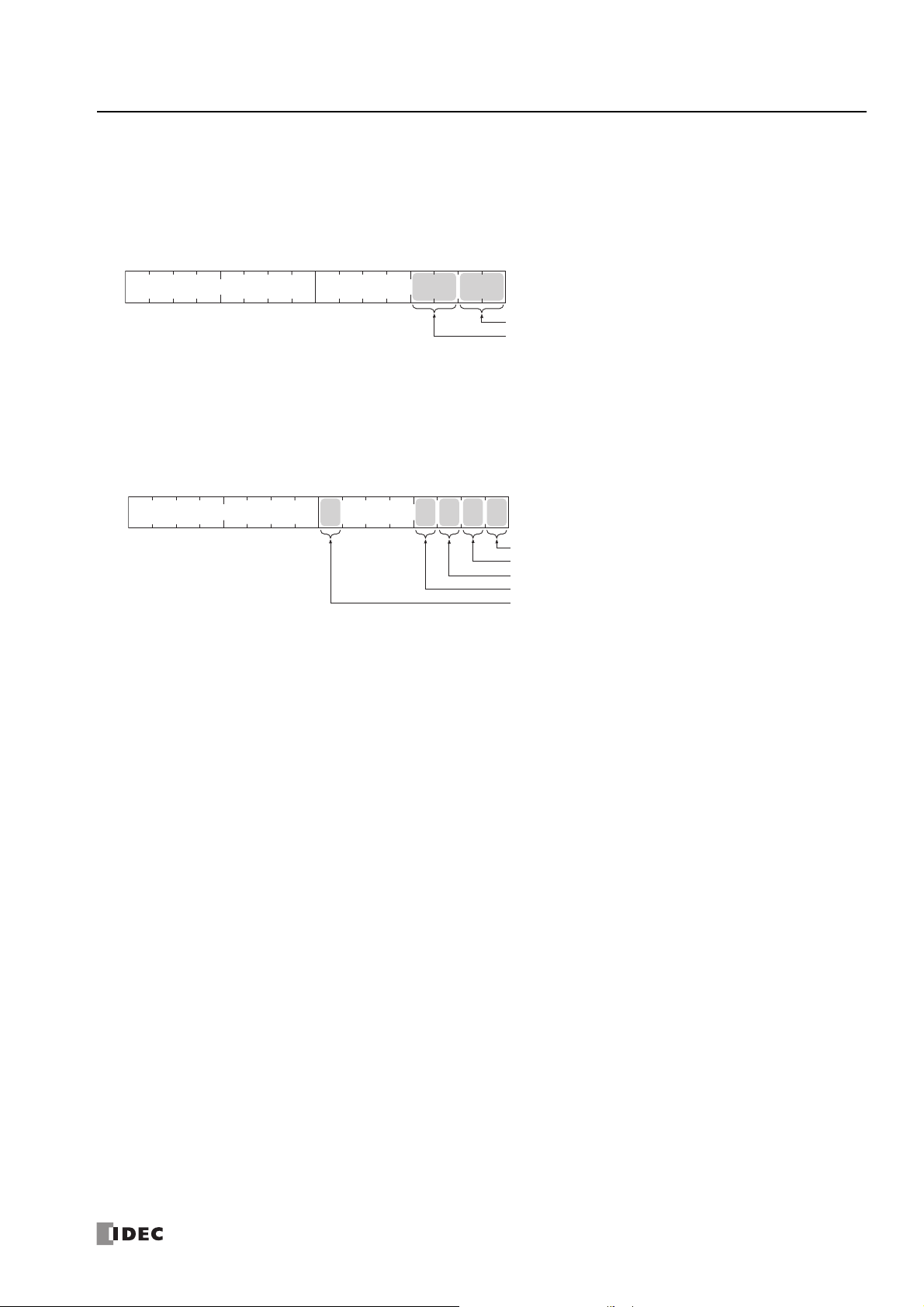
■ D8029: System Software Version
Bit
15
Bit
0
Bit
7
Bit
8
Bit
1
Bit
2
Bit
3
Port 2
Port 3
0 (00): No communication cartridges
1 (01): RS-232C communication cartridge
2 (10): RS-485 communication cartridge
3 (11): Free
Bit
15
Bit
0
Bit
7
Bit
8
1
Reserved=0
SD Memory Card
2
3
Cartridge Slot 1
Cartridge Slot 2
Cartridge Slot 3
0: No optional cartridge
1: Has optional cartridge
The CPU module system software version number is written to this register.
■ D8030: Communication Adapter Information
This register indicates information about the communication cartridges in Port 2 and Port 3.
The allocation of communication ports in the device (bit assignment) is as follows.
■ D8031: Optional Cartridge Connection Information
Optional cartridge connection information is written to this register.
The allocation of bits in the device (bit assignment) is as follows.
2: D
EVICES
■ D8032 to D8035, D8214, D8215: Interrupt Input Jump Destination Label No.
Jump destination label numbers for interrupt inputs are written to these registers. When using interrupt inputs, write the label
number that corresponds to the special data register that has been allocated to the interrupt input. For details on interrupt
inputs, see Chapter 5 "Interrupt Input" in the "FC6A Series MicroSmart All-in-One Type User’s Manual".
D8032 = I1
D8033 = I3
D8034 = I4
D8035 = I6
D8214 = I7
D8215 = I0
■ D8036: Timer Interrupt Jump Destination Label No.
The jump destination label number when the timer interrupt occurs is written to this register. When using the timer interrupt,
store the corresponding label number.
For details on the timer interrupt, see Chapter 5 "Timer Interrupt" in the "FC6A Series MicroSmart All-in-One Type User’s
Manual".
■ D8037: Number of Connected Expansion Modules
The number of expansion modules connected to the CPU module (expansion I/O modules and functional modules) is written to
this register.
■ D8052: J1939 Communication Error Code
When an error occurs in J1939 communication, the error code is written to this register. For details on J1939 communication
error codes, see Chapter 8 "J1939 Communication Error Code (D8052)" in the "FC6A Series MicroSmart All-in-One Type
Communication Manual".
■ D8056: Battery Voltage
The measurement result of the backup battery voltage is written to this register in 1 mV units.
0: Measurement error
■ D8057: Analog Volume (AI0)
The analog volume value is converted to a digital value and written to this register. For details, see Chapter 5 "Analog Volume"
in the "FC6A Series MicroSmart All-in-One Type User’s Manual".
FC6A S
ERIES MICROSMART
LAD P
ROGRAMMING MANUAL
FC9Y-B1726 2-21
Page 48

2: D
EVICES
■ D8058: Built-in Analog Input (AI1)
The analog input's analog value (0 to 10V DC) is converted to a digital value and written to this register. For details, see
Chapter 5 "Analog Voltage Input" in the "FC6A Series MicroSmart All-in-One Type User’s Manual".
■ D8059: Analog Input Status AI0
The analog volume's analog input status is written to this register. For details, see Chapter 5 "Analog Volume" in the "FC6A
Series MicroSmart All-in-One Type User’s Manual".
■ D8060: Analog Input Status AI1
The analog input's analog input status is written to this register. For details, see Chapter 5 "Analog Voltage Input" in the "FC6A
Series MicroSmart All-in-One Type User’s Manual".
■ D8067: Backlight ON Time
The backlight on time for the HMI module is written to this register. The backlight on time can be set by modifying the value of
D8067 in a range between 1 and 65,535 s. When D8067 is 0 s, the backlight is always on. The backlight on time can also be
changed with the HMI environment settings. For details, see Chapter 7 "Setting the LCD Backlight ON Time" in the "FC6A Series
MicroSmart All-in-One Type User’s Manual".
■ D8069 to D8099: Slave (1 to 31) Communication Status/Error
Special data registers used in data link communication. For details, see Chapter 7 "Master Station" in the "FC6A Series
MicroSmart All-in-One Type Communication Manual".
■ D8100, D8102, D8103: Slave Number (Port 1 to 3)
The slave number is written to these registers when the Port 1 to 3 communication mode is maintenance communication,
Modbus RTU slave, or data link communication. The slave number can be changed by changing the value of D8100, D8102, and
D8103 in Function Area Settings
D8100 = Port 1 Slave No.
D8102 = Port 2 Slave No.
D8103 = Port 3 Slave No.
For details on communication modes, see the following in the "FC6A Series MicroSmart All-in-One Type Communication Manual".
• Maintenance communication: Chapter 4 "Maintenance Communication"
• Modbus RTU slave: Chapter 6 "Modbus Communication"
• Data link communication: Chapter 7 "Data Link Communication"
2-22 FC6A S
ERIES MICROSMART
LAD P
ROGRAMMING MANUAL
FC9Y-B1726
Page 49

2: D
Port 1
Port 2
Port 3
Bit
15
Bit
0
Bit
7
Bit
8
12 3 45
0 (00): DTR and DSR are both off.
1 (01): DTR is off and DSR is on.
2 (10): DTR is on and DSR is off.
3 (11): DTR and DSR are both on.
ON
OFF
Not possible Not possiblePossible
DSR signal
Transmit/receive
ON
OFF
Not possible Not possiblePossible
DSR signal
Transmit/receive
ON
OFF
Not possible Not possiblePossible
DSR signal
Tra ns mit
Not possible Not possiblePossible
DSR signal
ON
OFF
Tra ns mit
■ D8104: Control Signal Status (Port 1 to 3)
The signal statuses of the DSR and DTR controls lines are written to this register. This register is updated in END processing
when stopped and while running. The allocation of communication ports in the device (bit assignment) is as follows.
■ D8105: RS232C DSR Input Control Signal Option (Port 1 to 3)
The signal statuses of the DSR and DTR controls lines are written to this register. This register is updated in END processing
when stopped and while running. The allocation of communication ports in the device (bit assignment) is as follows.
Bit
15
Bit
Bit
8
6
Bit
4
3
5
Bit
1
07
2
Port 1
Port 2
Port 3
EVICES
0 (000): The DSR signal status is not used for FC6A Series MicroSmart transmission control.
Use this status when DSR signal control is not required.
1 (001): When the DSR signal is on, the FC6A Series MicroSmart can transmit and receive.
2 (010): When the DSR signal is off, the FC6A Series MicroSmart can transmit and receive.
3 (011): When the DSR signal is on, transmission is possible (reception is always possible).
This is normally called "busy control" and is used for transmission control for devices with a slow
processing speed such as printers.
(As viewed from the connected device, there is a limit on the data that can be input.)
4 (100): When the DSR signal is off, transmission is possible.
5 or higher: The operation is the same as the setting "000".
FC6A S
ERIES MICROSMART
LAD P
ROGRAMMING MANUAL
FC9Y-B1726 2-23
Page 50

2: D
Port 1
Port 2
Port 3
Bit
15
Bit
0
Bit
7
Bit
8
1Bit 2
3
Bit 4
5
Running RunningStopped
DTR signal
ON
OFF
Not possible Not possiblePossible
DTR signal
ON
OFF
Receive
Status
Type ID
D8120
Reserved
System Software Version
D8121
Bit
15
Bit
0
Bit
7
Bit
8
12
34 5 6
910
1112
13
14
EVICES
■ D8106: RS232C DTR Output Control Signal Option (Port 1 to 3)
This register is used when indicating the FC6A Series MicroSmart control status and the transmit/receive status to the connected
device. This control line is an output signal from the FC6A Series MicroSmart to the connected device. This register is only valid
during user communication.
The allocation of communication ports in the device (bit assignment) is as follows.
0 (00): The signal is on when the FC6A Series MicroSmart is set to run and off when stopped.
While running, the signal is always on regardless of transmitting or receiving data. Set this value when it is
necessary to indicate the run status.
1 (01): Always off.
2 (10): Set this value when performing flow control for received data. The signal is on when data from the
connected device can be received.
The signal is off when data cannot be received.
3 (11): The operation is the same as the setting "0".
■ D8120, D8121: HMI Module Information
HMI module type information is written to these registers.
The allocation of information (bit assignment) is as follows.
The system software version displays the version of the software written to the device.
For details on the type IDs and statuses, see "List of Type IDs and Statuses" on page 2-31.
■ D8122 to D8127: Cartridge Slot Information
Cartridge Slot 1 to 3 information is written to these registers.
The allocation of information (bit assignment) is as follows.
Bit
12
0
D8122, D8124, D8126
D8123, D8125, D8127
Bit
Bit
15
15
13
14
1112
Status Type ID
Reserved System Software Version
Bit
Bit
910
7
8
34 5 6
D8122, D8123 = Cartridge Slot 1 Information
D8124, D8125 = Cartridge Slot 2 Information
D8126, D8127 = Cartridge Slot 3 Information
For details on the type IDs and statuses, see "List of Type IDs and Statuses" on page 2-31.
2-24 FC6A S
ERIES MICROSMART
LAD P
ROGRAMMING MANUAL
FC9Y-B1726
Page 51

2: D
Bit
15
Bit
0
Bit
7
Bit
8
1 2
3
Absolute Position Counter 1 Initialized Flag
Absolute Position Counter 2 Initialized Flag
Absolute Position Counter 3 Initialized Flag
Absolute Position Counter 4 Initialized Flag
0: Not initialized
1: Initialized
EVICES
■ D8170, D8171, D8174, D8175, D8178, D8179: Analog Cartridge I/O
Analog I/O values for the analog cartridges are written to these registers.
For the analog input type : The analog values input to the analog cartridge are converted to digital values and written to the
registers.
For the analog output type : The digital values stored as digital values are converted to analog values and output from the
analog cartridges.
For details, see Chapter 10 "Analog Cartridge" in the "FC6A Series MicroSmart All-in-One Type User’s Manual".
D8170 = AI2/AQ2
D8171 = AI3/AQ3
D8174 = AI4/AQ4
D8175 = AI5/AQ5
D8178 = AI6/AQ6
D8179 = AI7/AQ7
■ D8172, D8173, D8176, D8177, D8180, D8181: Analog Cartridge Status
The analog status of analog cartridges is written to these registers.
For details, see Chapter 10 "Analog Cartridge" in the "FC6A Series MicroSmart All-in-One Type User’s Manual".
D8172 = AI2/AQ2
D8173 = AI3/AQ3
D8176 = AI4/AQ4
D8177 = AI5/AQ5
D8180 = AI6/AQ6
D8181 = AI7/AQ7
■ D8192 to D8203, D8210 to D8213, D8216 to D8229, D8232 to D8237: High-speed Counter
These special data registers are used with the high-speed counter function and the frequency measurement function.
For details on high-speed counters, see Chapter 5 "High-Speed Counter" in the "FC6A Series MicroSmart All-in-One Type User’s
Manual".
D8210 to D8213, D8216, D8217 = High-speed counter (group 1/I0)
D8218 to D8221, D8234, D8235 = High-speed counter (group 3/I3)
D8222 to D8225, D8236, D8237 = High-speed counter (group 4/I4)
D8226 to D8229, D8232, D8233 = High-speed counter (group 5/I6)
D8192 to D8197 = High-speed counter (group 2/I1)
D8198 to D8203 = High-speed counter (group 6/I7)
■ D8239: Absolute Position Control Status
This register indicates the status of absolute position control.
The allocation of the absolute position counter initialized flags in the device (bit assignment) is as follows. For details on the
absolute position control status, see "ABS (Set Absolute Position)" on page 18-59.
■ D8240 to D8247: Absolute Position Counter 1 to 4
The absolute position is written to these registers according to pulse output. The absolute position can be initialized with the
ABS instruction.
When reversible control is set in the pulse output instructions (RAMP/ARAMP/ZRN/JOG), the absolute position is incremented or
decremented according to the output result. For details on absolute position counters, see "ABS (Set Absolute Position)" on page
18-59.
D8240, D8241 = Absolute position counter 1
D8242, D8243 = Absolute position counter 2
D8244, D8245 = Absolute position counter 3
D8246, D8247 = Absolute position counter 4
FC6A S
ERIES MICROSMART
LAD P
ROGRAMMING MANUAL
FC9Y-B1726 2-25
Page 52

2: D
EVICES
■ D8250: Read SD Memory Card Capacity
This register indicates the capacity of the recognized SD or SDHC (maximum size 32 GB) memory card in megabytes.
It is 0 when no SD memory card has been inserted or if it is not recognized.
■ D8251: Read SD Memory Card Free Capacity
This register indicates the free capacity of the SD memory card in megabytes.
It is 0 when no SD memory card has been inserted or if it is not recognized.
■ D8254: SD Memory Card Download/Upload Execution Information
Information about the SD memory card download/upload that was executed.
For details, see Chapter 11 "SD Memory Card" in the "FC6A Series MicroSmart All-in-One Type User’s Manual".
■ D8255: SD Memory Card Download/Upload Execution Status
The status of the SD memory card download/upload that was executed.
For details, see Chapter 11 "SD Memory Card" in the "FC6A Series MicroSmart All-in-One Type User’s Manual".
■ D8260: Recipe Block Number
The recipe block number to read or write using special internal relays.
All channels for the specified block number are applicable.
■ D8261: Recipe Execution Block Number
The recipe block number of the recipe that was executed.
This is updated when the recipe block starts, and the status is retained when completed.
■ D8262: Recipe Execution Channel No.
The channel number of the recipe that was executed.
This is updated when the channel processing starts, and the status is retained when completed.
■ D8263: Recipe Execution Operation
Information about the operation of the recipe that was executed.
For details on recipes, see Chapter 11 "Recipe Function" in the "FC6A Series MicroSmart All-in-One Type User’s Manual".
■ D8264: Recipe Execution Status
The status of the recipe that was executed.
For details on recipes, see Chapter 11 "Recipe Function" in the "FC6A Series MicroSmart All-in-One Type User’s Manual".
■ D8265: Recipe Execution Error Information
Error information about the recipe that was executed.
For details on recipes, see Chapter 11 "Recipe Function" in the "FC6A Series MicroSmart All-in-One Type User’s Manual".
■ D8278, D8279: Communication Mode Information (Client Connection) (Connection 1 to 8)
D8278 = Indicates the communication mode of connections 1 through 4.
D8279 = Indicates the communication mode of connections 5 through 8.
The allocation of connections in the device (bit assignment) is as follows.
D8278
D8279
Bit
15
Bit
15
Bit
Bit
7
8
Bit
Bit
7
8
Bit
0
Bit
0
Connection 1
Connection 2
Connection 3
Connection 4
• Client connection (most significant bit = 0)
0000: Unused
0001: User Communication
0010: Modbus TCP client
2-26 FC6A S
ERIES MICROSMART
LAD P
ROGRAMMING MANUAL
Connection 5
Connection 6
Connection 7
Connection 8
FC9Y-B1726
Page 53

• Server connection (most significant bit = 1)
Bit
15
Bit
0
Bit
7
Bit
8
HMI Connection 1
HMI Connection 2
HMI Connection 3
HMI Connection 4
D8284
Bit
15
Bit
0
Bit
7
Bit
8
HMI Connection 5
HMI Connection 6
HMI Connection 7
HMI Connection 8
D8285
1000: Maintenance Communication
1001: User Communication
1010: Modbus TCP server
■ D8284, D8285: Communication Mode Information (HMI Connection) (HMI Connection 1 to 8)
D8284: Indicates the communication mode of HMI connections 1 through 4.
D8285: Indicates the communication mode of HMI connections 5 through 8.
The allocation of connections in the device (bit assignment) is as follows.
2: D
EVICES
• Client connection (most significant bit = 0)
0000: Unused
• Server connection (most significant bit = 1)
1000: Maintenance Communication
■ D8304 to D8307: CPU Module IP Address (Write-only)
These registers are used to write the CPU module's IP address.
IP address: To set as aaa.bbb.ccc.ddd, write the following.
D8304=aaa, D8305=bbb, D8306=ccc, D8307=ddd
■ D8308 to D8311: CPU Module Subnet Mask (Write-only)
These registers are used to write the CPU module's subnet mask.
Subnet mask: For aaa.bbb.ccc.ddd, write the following.
D8308=aaa, D8309=bbb, D8310=ccc, D8311=ddd
■ D8312 to D8315: CPU Module Default Gateway (Write-only)
These registers are used to write the CPU module's default gateway.
Default gateway: For aaa.bbb.ccc.ddd, write the following.
D8312=aaa, D8313=bbb, D8314=ccc, D8315=ddd
■ D8316 to D8319: CPU Module Preferred DNS Server (Write-only)
These registers are used to write the CPU module's preferred DNS server.
Preferred DNS server: For aaa.bbb.ccc.ddd, write the following.
D8316=aaa, D8317=bbb, D8318=ccc, D8319=ddd
■ D8320 to D8323: CPU Module Alternate DNS Server (Write-only)
These registers are used to write the CPU module's alternate DNS server.
Alternate DNS server: For aaa.bbb.ccc.ddd, write the following.
D8320=aaa, D8321=bbb, D8322=ccc, D8323=ddd
■ D8324 to D8329: CPU Module MAC Address (Current Value Read-only)
The CPU module's MAC address is written to the special data registers as follows.
Example: MAC address: AA-BB-CC-DD-EE-FF
D8324=AA, D8325=BB, D8326=CC, D8327=DD, D8328=EE, D8329=FF
FC6A S
ERIES MICROSMART
LAD P
ROGRAMMING MANUAL
FC9Y-B1726 2-27
Page 54

2: D
EVICES
■ D8330 to D8333: CPU Module IP Address (Current Value Read-only)
The CPU module's IP address is written to the special data registers as follows.
Example: The CPU module's own IP address aaa.bbb.ccc.ddd
D8330=aaa, D8331=bbb, D8332=ccc, D8333=ddd
■ D8334 to D8337: CPU Module Subnet Mask (Current Value Read-only)
The CPU module's subnet mask value is written to the special data registers as follows.
Example: Subnet mask: aaa.bbb.ccc.ddd
D8334=aaa, D8335=bbb, D8336=ccc, D8337=ddd
■ D8338 to D8341: CPU Module Default Gateway (Current Value Read-only)
The CPU module's default gateway address is written to the special data registers as follows.
Example: Default gateway: aaa.bbb.ccc.ddd
D8338=aaa, D8339=bbb, D8340=ccc, D8341=ddd
■ D8342 to D8345: CPU Module Preferred DNS Server (Current Value Read-only)
The CPU module's preferred DNS server address is written to the special data registers as follows.
Example: Preferred DNS server: aaa.bbb.ccc.ddd
D8342=aaa, D8343=bbb, D8344=ccc, D8345=ddd
■ D8346 to D8349: CPU Module Alternate DNS Server (Current Value Read-only)
The CPU module's alternate DNS server address is written to the special data registers as follows.
Example: Alternate DNS server: aaa.bbb.ccc.ddd
D8346=aaa, D8347=bbb, D8348=ccc, D8349=ddd
■ D8350 to D8381: Connection Connected IP Address
The IP address of the connected device that is being accessed through a connection is written as follows.
Connection 1 Connected IP Address: For aaa.bbb.ccc.ddd
D8350=aaa, D8351=bbb, D8352=ccc, D8353=ddd
Connection 2 Connected IP Address: For aaa.bbb.ccc.ddd
D8354=aaa, D8355=bbb, D8356=ccc, D8357=ddd
Connection 3 Connected IP Address: For aaa.bbb.ccc.ddd
D8358=aaa, D8359=bbb, D8360=ccc, D8361=ddd
Connection 4 Connected IP Address: For aaa.bbb.ccc.ddd
D8362=aaa, D8363=bbb, D8364=ccc, D8365=ddd
Connection 5 Connected IP Address: For aaa.bbb.ccc.ddd
D8366=aaa, D8367=bbb, D8368=ccc, D8369=ddd
Connection 6 Connected IP Address: For aaa.bbb.ccc.ddd
D8370=aaa, D8371=bbb, D8372=ccc, D8373=ddd
Connection 7 Connected IP Address: For aaa.bbb.ccc.ddd
D8374=aaa, D8375=bbb, D8376=ccc, D8377=ddd
Connection 8 Connected IP Address: For aaa.bbb.ccc.ddd
D8378=aaa, D8379=bbb, D8380=ccc, D8381=ddd
■ D8382 to D8387: HMI Module MAC Address (Current Value Read-only)
The MAC address is written to the special data registers as follows.
Example: MAC address: AA-BB-CC-DD-EE-FF
D8382=AA, D8383=BB, D8384=CC, D8385=DD, D8386=EE, D8387=FF
■ D8388 to D8391: HMI Module IP Address (Current Value Read-only)
The HMI module's IP address is written to the special data registers as follows.
Example: HMI module IP address: aaa.bbb.ccc.ddd
D8388=aaa, D8389=bbb, D8390=ccc, D8391=ddd
■ D8392 to D8395: HMI Module Subnet Mask (Current Value Read-only)
The HMI module's subnet mask value is written to the special data registers as follows.
Example: HMI module subnet mask: aaa.bbb.ccc.ddd
D8392=aaa, D8393=bbb, D8394=ccc, D8395=ddd
2-28 FC6A S
ERIES MICROSMART
LAD P
ROGRAMMING MANUAL
FC9Y-B1726
Page 55

2: D
EVICES
■ D8396 to D8399: HMI Module Default Gateway (Current Value Read-only)
The HMI module's default gateway address is written to the special data registers as follows.
Example: HMI module default gateway: aaa.bbb.ccc.ddd
D8396=aaa, D8397=bbb, D8398=ccc, D8399=ddd
■ D8400 to D8403: HMI Module Preferred DNS Server (Current Value Read-only)
The HMI module's preferred DNS server address is written to the special data registers as follows.
Example: HMI module preferred DNS server: aaa.bbb.ccc.ddd
D8400=aaa, D8401=bbb, D8402=ccc, D8403=ddd
■ D8404 to D8407: HMI Module Alternate DNS Server (Current Value Read-only)
The HMI module's alternate DNS server address is written to the special data registers as follows.
Example: HMI module alternate DNS server: aaa.bbb.ccc.ddd
D8404=aaa, D8405=bbb, D8406=ccc, D8407=ddd
■ D8413: Time Zone Offset
The time zone configured in the function area settings can be finely adjusted in 15-minute increments.
For details, see Chapter 3 "SNTP Settings" in the "FC6A Series MicroSmart All-in-One Type Communication Manual".
■ D8414: SNTP Operation Status
The operation status is written to this register when the time information is acquired through operation of M8191 (SNTP Time
Acquisition Flag) or when time information acquisition was executed by automatic acquisition.
For details, see Chapter 3 "SNTP Settings" in the "FC6A Series MicroSmart All-in-One Type Communication Manual".
■ D8415: SNTP Access Elapsed Time
The elapsed time in minutes from when the time information was last acquired from the SNTP server.
For details, see Chapter 3 "SNTP Settings" in the "FC6A Series MicroSmart All-in-One Type Communication Manual".
■ D8429: HMI Module Connection Information Reference Connection Number
The connection information for the specified connection number is reflected in D8430 to D8434. When 0 is written, 0 is written
to D8430 to D8434. If a connection number that does not exist is specified, 0 is written to D8430 to D8434.
■ D8430 to D8433: HMI Module Connection Information Reference Connected IP Address
The IP address of the terminal being accessed through the connection is written to the special data registers as follows.
Example: IP address to read: aaa.bbb.ccc.ddd
D8430=aaa, D8431=bbb, D8432=ccc, D8433=ddd
■ D8434: HMI Module Connection Information Reference Connected Port No.
The port number of the terminal being accessed through the connection is written to this register.
■ D8437 to D8440: HMI Module IP Address (Write-only)
These registers are used to write the HMI module's IP address.
HMI module IP address: To set as aaa.bbb.ccc.ddd, write the following.
D8437=aaa, D8438=bbb, D8439=ccc, D8440=ddd
■ D8441 to D8444: HMI Module Subnet Mask (Write-only)
These registers are used to write the HMI module's subnet mask.
HMI module subnet mask: For aaa.bbb.ccc.ddd, write the following.
D8441=aaa, D8442=bbb, D8443=ccc, D8444=ddd
■ D8445 to D8448: HMI Module Default Gateway (Write-only)
These registers are used to write the HMI module's default gateway.
HMI module default gateway: For aaa.bbb.ccc.ddd, write the following.
D8445=aaa, D8446=bbb, D8447=ccc, D8448=ddd
■ D8449 to D8452: HMI Module Preferred DNS Server (Write-only)
These registers are used to write the HMI module's preferred DNS server.
HMI module preferred DNS server: For aaa.bbb.ccc.ddd, write the following.
D8449=aaa, D8450=bbb, D8451=ccc, D8452=ddd
■ D8453 to D8456: HMI Module Alternate DNS Server (Write-only)
These registers are used to write the HMI module's alternate DNS server.
HMI module alternate DNS server: For aaa.bbb.ccc.ddd, write the following.
D8453=aaa, D8454=bbb, D8455=ccc, D8456=ddd
FC6A S
ERIES MICROSMART
LAD P
ROGRAMMING MANUAL
FC9Y-B1726 2-29
Page 56

2: D
EVICES
■ D8457: EMAIL Instruction Detailed Error Information
Detailed error information for the EMAIL instruction is written to this register.
For details, see Chapter 10 "Confirm the error detail of EMAIL instruction" in the "FC6A Series MicroSmart All-in-One Type
Communication Manual".
■ D8470 to D8499: Expansion Module Slot Information
Expansion module type information is written to these registers.
The allocation of information (bit assignment) is as follows.
Bit
15
Upper Status Type ID
13
14
1112
Bit7Bit
910
8
34 5 6
Bit
12
0
Lower
Reserved System Software Version
Upper Lower
D8470, D8471 = Expansion Module Slot 1 Information
D8472, D8473 = Expansion Module Slot 2 Information
D8474, D8475 = Expansion Module Slot 3 Information
D8476, D8477 = Expansion Module Slot 4 Information
D8478, D8479 = Expansion Module Slot 5 Information
D8480, D8481 = Expansion Module Slot 6 Information
D8482, D8483 = Expansion Module Slot 7 Information
D8484, D8485 = Expansion Module Slot 8 Information
D8486, D8487 = Expansion Module Slot 9 Information
D8488, D8489 = Expansion Module Slot 10 Information
D8490, D8491 = Expansion Module Slot 11 Information
D8492, D8493 = Expansion Module Slot 12 Information
D8494, D8495 = Expansion Module Slot 13 Information
D8496, D8497 = Expansion Module Slot 14 Information
D8498, D8499 = Expansion Module Slot 15 Information
For details on the type IDs and statuses, see "List of Type IDs and Statuses" on page 2-31.
2-30 FC6A S
ERIES MICROSMART
LAD P
ROGRAMMING MANUAL
FC9Y-B1726
Page 57

List of Type IDs and Statuses
■ Type ID
Expansion module and HMI module
Type ID
Hexadecimal Binary
0x00 0000 0000 FC6A-N16B1, FC6A-N16B3
0x01 0000 0001 FC6A-R161, FC6A-T16K1, FC6A-T16P1, FC6A-T16K3, FC6A-T16P3
0x02 0000 0010 FC6A-N32B3
0x03 0000 0011 FC6A-T32K3, FC6A-T32P3
0x04 0000 0100 FC6A-N08B1, FC6A-N08A11
0x05 0000 0101 FC6A-R081, FC6A-T08K1, FC6A-T08P1
0x06 0000 0110 FC6A-M08BR1
0x07 0000 0111 FC6A-M24BR1
0x18 0001 1000 FC6A-PH1
0x19 0001 1001 FC6A-EXM2
0x20 0010 0000 FC6A-J2C1
0x21 0010 0001 FC6A-J4A1
0x22 0010 0010 FC6A-J8A1
0x24 0010 0100 FC6A-K4A1
0x25 0010 0101 FC6A-L06A1
0x26 0010 0110 FC6A-L03CN1
0x27 0010 0111 FC6A-J4CN1
0x28 0010 1000 FC6A-J8CU1
0x29 0010 1001 FC6A-F2M1
0x2A 0010 1010 FC6A-F2MR1
0xFF 1111 1111 Not connected
Type No.
2: D
EVICES
Cartridge
Type ID
Hexadecimal Binary
0x00 0000 0000 FC6A-PJ2A
0x01 0000 0001 FC6A-PK2AV
0x02 0000 0010 FC6A-PK2AW
0x03 0000 0011 FC6A-PJ2CP
0x06 0000 0110 FC6A-PC1
0x07 0000 0111 FC6A-PC3
0xFF 1111 1111 Not connected
Type No.
■ Status
Status
Hexadecimal Binary
0x00 0000 0000 Normal
0x81 1000 0001
0x82 1000 0010 Unknown device detected (A device other than the FC6A Series MicroSmart is connected.)
0x83 1000 0011
0x84 1000 0100 Device writing error (The attempt to set the operation of the device failed.)
0x85 1000 0101 System update error (The system update failed.)
Communication error (An error has occurred in the communication between the CPU module and an
expansion module, HMI module, or cartridge.)
Device setting error (No device is connected or the connected device is different from that set in the
user program.)
Description
FC6A S
ERIES MICROSMART
LAD P
ROGRAMMING MANUAL
FC9Y-B1726 2-31
Page 58

2: D
EVICES
2-32 FC6A S
ERIES MICROSMART
LAD P
ROGRAMMING MANUAL
FC9Y-B1726
Page 59

3: I
NSTRUCTIONS
R
EFERENCE
Introduction
This chapter provides a list of FC6A Series MicroSmart instructions and describes their functions.
The instructions are divided into basic instructions, which perform sequencing, and advanced instructions, which perform moves,
comparisons, Boolean computations, binary arithmetic operations, bit shifts, and other operations.
Basic Instruction List
Symbol Name Function See Page
AND And Series connection of NO contact 4-4
AND LOD And Load Series connection of circuit blocks 4-5
ANDN And Not Series connection of NC contact 4-4
BPP Bit Pop Restores the result of bit logical operation which was saved temporarily 4-6
BPS Bit Push Saves the result of bit logical operation temporarily 4-6
BRD Bit Read Reads the result of bit logical operation which was saved temporarily 4-6
CC= Counter Comparison (=) Equal to comparison of counter current value 4-18
CC>= Counter Comparison (>=) Greater than or equal to comparison of counter current value 4-18
CDP Dual Pulse Reversible Counter Dual pulse reversible counter (0 to 65,535) 4-11
CDPD
CNT Adding Counter Adding counter (0 to 65,535) 4-11
CNTD Double-Word Adding Counter Double-word adding counter (0 to 4,294,967,295) 4-14
CUD
CUDD
DC= Data Register Comparison (=) Equal to comparison of data register value 4-20
DC>= Data Register Comparison (>=) Greater than or equal to comparison of data register value 4-20
END End Ends a program 4-30
JEND Jump End Ends a jump instruction 4-29
JMP Jump Jumps a designated program area 4-29
LOD Load Stores intermediate results and reads contact status 4-1
LODN Load Not Stores intermediate results and reads inverted contact status 4-1
MCR Master Control Reset Ends a master control 4-27
MCS Master Control Set Starts a master control 4-27
OR Or Parallel connection of NO contact 4-4
OR LOD Or Load Parallel connection of circuit blocks 4-5
ORN Or Not Parallel connection of NC contact 4-4
OUT Output Outputs the result of bit logical operation 4-1
OUTN Output Not Outputs the inverted result of bit logical operation 4-1
RST Reset Resets output, internal relay, or shift register bit 4-3
SET Set Sets output, internal relay, or shift register bit 4-3
SFR Shift Register Forward shift register 4-22
SFRN Shift Register Not Reverse shift register 4-22
SOTD Single Output Down Falling-edge differentiation output 4-26
SOTU Single Output Up Rising-edge differentiation output 4-26
TIM 100-ms Timer Subtracting 100-ms timer (0 to 6,553.5 s) 4-7
TIMO 100-ms Off-delay Timer Subtracting 100-ms off-delay timer (0 to 6,553.5 s) 4-10
Double-Word Dual Pulse
Reversible Counter
Up/Down Selection
Reversible Counter
Double-Word Up/Down
Selection Reversible Counter
Double-word dual pulse reversible counter (0 to 4,294,967,295) 4-14
Up/down selection reversible counter (0 to 65,535) 4-11
Double-word up/down selection reversible counter
(0 to 4,294,967,295)
4-14
FC6A S
ERIES MICROSMART
LAD P
ROGRAMMING MANUAL
FC9Y-B1726 3-1
Page 60

3: I
NSTRUCTIONS REFERENCE
Symbol Name Function See Page
TMH 10-ms Timer Subtracting 10-ms timer (0 to 655.35 s) 4-7
TMHO 10-ms Off-delay Timer Subtracting 10-ms off-delay timer (0 to 655.35 s) 4-10
TML 1-s Timer Subtracting 1-s timer (0 to 65,535 s) 4-7
TMLO 1-s Off-delay Timer Subtracting 1-s off-delay timer (0 to 65,535 s) 4-10
TMS 1-ms Timer Subtracting 1-ms timer (0 to 65.535 s) 4-7
TMSO 1-ms Off-delay Timer Subtracting 1-ms off-delay timer (0 to 65.535 s) 4-10
3-2 FC6A S
ERIES MICROSMART
LAD P
ROGRAMMING MANUAL
FC9Y-B1726
Page 61

Advanced Instruction List
3: I
NSTRUCTIONS REFERENCE
Group Symbol Name
NOP NOP No Operation 3-11
MOV Move XXXXX 5-1
MOVN Move Not X X X X 5-5
IMOV Indirect Move X X X 5-6
IMOVN Indirect Move Not X X 5-8
BMOV Block Move X 5-9
Move
Data Comparison
Binary Arithmetic
Boolean Computation
Shift and Rotate
IBMV Indirect Bit Move X 5-10
IBMVN Indirect Bit Move Not X 5-12
NSET N Data Set X X X X X 5-13
NRS N Data Repeat Set X X X X X 5-14
XCHG Exchange X X 5-15
TCCST Timer/Counter Current Value Store X X 5-16
CMP= Compare Equal To XXXXX 6-1
CMP<> Compare Unequal To XXXXX 6-1
CMP< Compare Less Than XXXXX 6-1
CMP> Compare Greater Than XXXXX 6-1
CMP<= Compare Less Than or Equal To XXXXX 6-1
CMP>= Compare Greater Than or Equal To XXXXX 6-1
ICMP>= Interval Compare Greater Than or Equal To XXXXX 6-6
LC= Load Compare Equal To XXXXX 6-8
LC<> Load Compare Unequal To XXXXX 6-8
LC< Load Compare Less Than XXXXX 6-8
LC> Load Compare Greater Than XXXXX 6-8
LC<= Load Compare Less Than or Equal To XXXXX 6-8
LC>= Load Compare Greater Than or Equal To XXXXX 6-8
ADD Addition XXXXX 7-1
SUB Subtraction XXXXX 7-1
MUL Multiplication X X X X X 7-1
DIV Division X X X X X 7-1
INC Increment X X X X 7-13
DEC Decrement XXXX 7-13
ROOT Root X X X 7-14
SUM
RNDM
ANDW AND Word X X 8-1
ORW OR Word X X 8-1
XORW Exclusive OR Word X X 8-1
SFTL Shift Left 9-1
SFTR Shift Right 9-3
BCDLS BCD Left Shift X 9-5
WSFT Word Shift X 9-7
ROTL Rotate Left X X 9-8
ROTR Rotate Right X X 9-10
Sum (ADD) X X X X X 7-15
Sum (XOR) X 7-15
Random X 7-18
Valid Data Type
WI D L F
See Page
FC6A S
ERIES MICROSMART
LAD P
ROGRAMMING MANUAL
FC9Y-B1726 3-3
Page 62

3: I
NSTRUCTIONS REFERENCE
Group Symbol Name
Data Conversion
Week Programmer
Interface
Program Branching
Coordinate Conversion
Pulse
PID Control
Valid Data Type
WI D L F
HTOB Hex to BCD X X 10-1
BTOH BCD to Hex X X 10-3
HTOA Hex to ASCII X 10-5
ATOH ASCII to Hex X 10-7
BTOA BCD to ASCII X X 10-9
ATOB ASCII to BCD X X 10-12
ENCO Encode 10-15
DECO Decode 10-16
BCNT Bit Count 10-17
ALT Alternate Output 10-18
CVDT Convert Data Type XXXXX 10-19
DTDV Data Divide X 10-21
DTCB Data Combine X 10-22
SWAP Data Swap X X 10-23
WKTIM Week Timer 11-1
WKTBL Week Table 11-1
WEEK Weekly Timer 11-3
YEAR Yearly Timer 11-16
MSG Message 12-1
DISP Display 12-20
DGRD Digital Read 12-22
LABEL Label 13-1
LJMP Label Jump 13-1
LCAL Label Call 13-3
LRET Label Return 13-3
DJNZ Decrement Jump Non-zero 13-5
DI Disable Interrupt 15-1
EI Enable Interrupt 15-1
IOREF I/O Refresh 14-1
HSCRF High-speed Counter Refresh 14-3
FRQRF Frequency Measurement Refresh 14-4
COMRF Communication Refresh 14-5
XYFS XY Format Set X X 16-1
CVXTY Convert X to Y X X 16-2
CVYTX Convert Y to X X X 16-3
AVRG Average XXXXX 17-1
PULS1 Pulse Output 1 18-1
PULS2 Pulse Output 2 18-1
PULS3 Pulse Output 3 18-1
PULS4 Pulse Output 4 18-1
PWM1 Pulse Width Modulation 1 18-8
PWM2 Pulse Width Modulation 2 18-8
PWM3 Pulse Width Modulation 3 18-8
PWM4 Pulse Width Modulation 4 18-8
RAMP1 Ramp Pulse Output 1 18-15
RAMP2 Ramp Pulse Output 2 18-15
ZRN1 Zero Return 1 18-27
ZRN2 Zero Return 2 18-27
ARAMP1 Advanced Ramp 1 18-37
ARAMP2 Advanced Ramp 2 18-37
ABS Set Absolute Position 18-59
JOG JOG Operation 18-63
PID PID Control (FC5A compatible) 19-1
PIDA PID Control 19-3
PIDD PID with Derivative Decay 19-26
See Page
3-4 FC6A S
ERIES MICROSMART
LAD P
ROGRAMMING MANUAL
FC9Y-B1726
Page 63

3: I
NSTRUCTIONS REFERENCE
Group Symbol Name
DTML 1-s Dual Timer 20-1
DTIM 100-ms Dual Timer 20-1
Dual / Teaching Timer
Trigonometric Function
Logarithm / Power
File Data Processing
Clock
Data Logging
Script SCRPT Script XXXXX 26-1
Flow Volume Calculation
User-defined Macro UMACRO User-defined Macro 28-1
User Communication
PING PING Ping
E-mail EMAIL Send E-mail
DTMH 10-ms Dual Timer 20-1
DTMS 1-ms Dual Timer 20-1
TTIM Teaching Timer 20-3
RAD Degree to Radian X 21-1
DEG Radian to Degree X 21-2
SIN Sine X 21-3
COS Cosine X 21-4
TAN Tangent X 21-5
ASIN Arc Sine X 21-6
ACOS Arc Cosine X 21-7
ATAN Arc Tangent X 21-8
LOGE Natural Logarithm X 22-1
LOG10 Common Logarithm X 22-2
EXP Exponent X 22-3
POW Power X 22-4
FIFOF FIFO Format X 23-1
FIEX First-In Execute X 23-3
FOEX First-Out Execute X 23-3
NDSRC N Data Search XXXXX 23-5
TADD Time Addition 24-1
TSUB Time Subtraction 24-5
HTOS HMS to S 24-9
STOH S to HMS 24-10
HOUR Hour Meter 24-11
DLOG Data Logging 25-1
TRACE Data Trace 25-7
SCALE Convert Analog Input X X 27-1
FLWA Analog Flow Totalizer 27-9
FLWP Pulse Flow Totalizer X X 27-18
TXD2 Transmit 2
TXD3 Transmit 3
RXD2 Receive 2
RXD3 Receive 3
Valid Data Type
WI D L F
See Page
Communication
Manual
5-2
Communication
Manual
5-2
Communication
Manual
5-10
Communication
Manual
5-10
Communication
Manual
9-1
Communication
Manual
10-1
FC6A S
ERIES MICROSMART
LAD P
ROGRAMMING MANUAL
FC9Y-B1726 3-5
Page 64
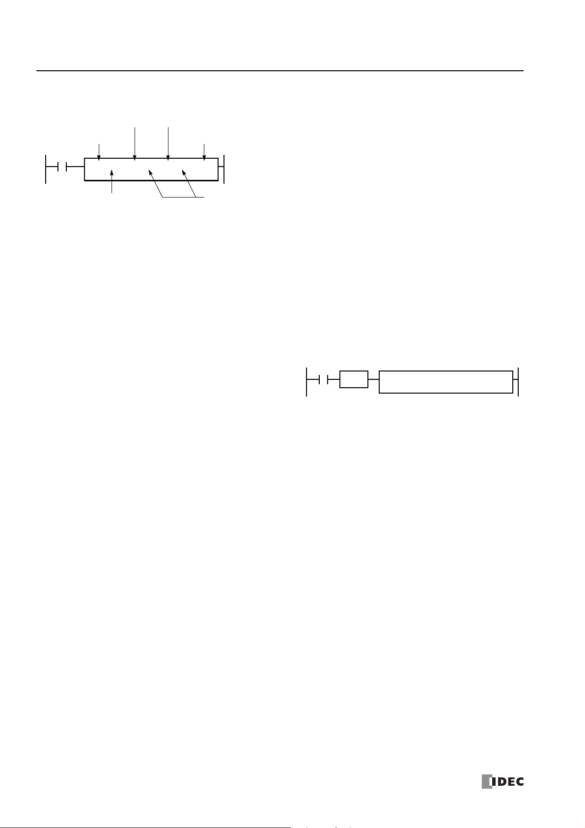
3: I
I0
S1 R
*****
REP
**
D1 R
*****
Opcode
Source Device
Repeat Cycles
Destination Device
Repeat
MOV(W)
Data Type
Designation
I0
REPS1 –
D10
D1 –
D20
SOTU
MOV(W)
NSTRUCTIONS REFERENCE
Structure of an Advanced Instruction
Opcode
The opcode is a symbol used to identify the advanced instruction.
Data Type
Specifies word (W), integer (I), double word (D), long (L), or float
(F) data.
Source Device
The source device specifies the 16- or 32-bit data to be processed
by the advanced instruction. Some advanced instructions require
two source devices.
Repeat Designation
Specifies whether repeat is used for the device or not.
Repeat Cycles
Specifies the quantity of repeat cycles: 1 through 99.
Destination Device
The destination device specifies the 16- or 32-bit data to store the
result of the advanced instruction. Some advanced instructions
require two destination devices.
Input Condition for Advanced Instructions
Almost all advanced instructions must be preceded by a contact, except NOP (no operation), LABEL (label), and LRET (label
return) instructions. The input condition can be programmed using a bit device such as input, output, internal relay, or shift
register. Timer and counter can also be used as an input condition to turn on the contact when the timer times out or the counter
counts out.
While the input condition is on, the advanced instruction is
executed in each scan. To execute the advanced instruction
only at the rising or falling edge of the input, use the SOTU or
SOTD instruction.
While the input condition is off, the advanced instruction is not executed and device statuses are held.
Source and Destination Devices
The source and destination devices specify 16- or 32-bit data, depending on the selected data type. When a bit device such as
input, output, internal relay, or shift register is designated as a source or destination device, 16 or 32 points starting with the
designated number are processed as source or destination data. When a word device such as timer or counter is designated as a
source device, the current value is read as source data. When a timer or counter is designated as a destination device, the result
of the advanced instruction is set to the preset value for the timer or counter. When a data register is designated as a source or
destination device, the data is read from or written to the designated data register.
Using Timer or Counter as Source Device
Since all timer instructions—TML (1-s timer), TIM (100-ms timer), TMH (10-ms timer), and TMS (1-ms timer) — subtract from the
preset value, the current value is decremented from the preset value and indicates the remaining time. As described above, when
a timer is designated as a source device of an advanced instruction, the current value, or the remaining time, of the timer is read
as source data. Adding counters CNT start counting at 0, and the current value is incremented up to the preset value. Reversible
counters CDP and CUD start counting at the preset value and the current value is incremented or decremented from the preset
value. When any counter is designated as a source device of an advanced instruction, the current value is read as source data.
Using Timer or Counter as Destination Device
As described above, when a timer or counter is designated as a destination device of an advanced instruction, the result of the
advanced instruction is set to the preset value of the timer or counter. Timer and counter preset values can be 0 through 65,535.
When a timer or counter preset value is designated using a data register, the timer or counter cannot be designated as a
destination of an advanced instruction. When executing such an advanced instruction, a user program execution error will
result. For details of user program execution error, see Chapter 13 "User Program Execution Error" in the "FC6A Series
MicroSmart All-in-One Type User's Manual".
Note: When a user program execution error occurs, the result is not set to the destination.
3-6 FC6A S
ERIES MICROSMART
LAD P
ROGRAMMING MANUAL
FC9Y-B1726
Page 65

3: I
NSTRUCTIONS REFERENCE
Data Types for Advanced Instructions
When using move, data comparison, binary arithmetic, Boolean computation, bit shift/rotate, data conversion, and coordinate
conversion instructions, data types can be selected from word (W), integer (I), double word (D), long (L), or float (F). For other
advanced instructions, the data is processed in units of 16-bit word.
Data Type Symbol Bits
Word (Unsigned 16 bits) W 16 bits 1 0 to 65,535 $0000 to $FFFF
Integer (Signed 16 bits) I 16 bits 1 –32,768 to 32,767 $8000 to $7FFF
Double Word (Unsigned 32 bits) D 32 bits 2 0 to 4,294,967,295
Long (Signed 32 bits) L 32 bits 2
Float (Floating point) F 32 bits 2
• When a constant is set in WindLDR, it can be set as decimal or hexadecimal number. Prefix the number with "$" to set it as a hexadecimal
number.
Quantity of Data
Registers Used
Range of Decimal Values
Decimal Hexdecimal
$00000000 to
–2,147,483,648 to
2,147,483,647
–3.402823×1038 to
3.402823×10
38
$80000000 to
$FFFFFFFF
$7FFFFFFF
—
Decimal Values and Hexadecimal Storage (Word, Integer, Double, and Long Data)
The following table shows hexadecimal equivalents which are stored in the CPU, as a result of addition and subtraction of the
decimal values shown:
Data Type Result of Addition Hexadecimal Storage Result of Subtraction Hexadecimal Storage
Word
Integer
Double Word
Long
0
65,535
131,071
65,534
32,768
32,767
0
–1
–32,767
–32,768
–32,769
–65,535
0
4,294,967,295
8,589,934,591
4,294,967,294
2,147,483,648
2,147,483,647
0
–1
–2,147,483,647
–2,147,483,648
–2,147,483,649
–4,294,967,295
0000
FFFF
(CY) FFFF
(CY) 7FFE
(CY) 0000
7FFF
0000
FFFF
8001
8000
(CY) FFFF
(CY) 8001
00000000
FFFFFFFF
(CY) FFFFFFFF
(CY) 7FFFFFFE
(CY) 00000000
7FFFFFFF
00000000
FFFFFFFF
80000001
80000000
(CY) FFFFFFFF
(CY) 80000001
65,535
0
–1
–65,535
–65,536
65,534
32,768
32,767
0
–1
–32,767
–32,768
–32,769
–65,535
4,294,967,295
0
–1
–4,294,967,295
–4,294,967,296
4,294,967,294
2,147,483,648
2,147,483,647
0
–1
–2,147,483,647
–2,147,483,648
–2,147,483,649
–4,294,967,295
FFFF
0000
(BW) FFFF
(BW) 0001
(BW) 0000
(BW) 7FFE
(BW) 0000
7FFF
0000
FFFF
8001
8000
(BW) FFFF
(BW) 8001
FFFFFFFF
00000000
(BW) FFFFFFFF
(BW) 00000001
(BW) 00000000
(BW) 7FFFFFFE
(BW) 00000000
7FFFFFFF
00000000
FFFFFFFF
80000001
80000000
(BW) FFFFFFFF
(BW) 80000001
FC6A S
ERIES MICROSMART
LAD P
ROGRAMMING MANUAL
FC9Y-B1726 3-7
Page 66

3: I
s e[30:23] f[22:0]
31 30 23 22 0
23-bit fraction8-bit biased exponent
Sign bit (0: positive, 1: negative)
0≠
0
–1.175495×10
–38
M8003
1 1
1.175495×10
–38
0–3.402823×10
38
0
Execution Result
1
Overflow
0 1
3.402823×10
38
Overflow
Not Zero
NSTRUCTIONS REFERENCE
Floating-Point Data Format
The FC6A Series MicroSmart can specify floating-point data (F) for advanced instructions. Like double word (D) and long integer
(L) data, floating-point data also uses two consecutive data registers to execute advanced instructions. The FC6A Series
MicroSmart supports the floating-point data based on the single storage format of the IEEE (The Institute of Electrical and
Electronics Engineers) Standard 754.
Single Storage Format
The IEEE single storage format consists of three fields: a 23-bit fraction, f; an 8-bit biased exponent, e; and 1-bit sign, s. These
fields are stored contiguously in one 32-bit word, as shown in the figure below. Bits 0:22 contain the 23-bit fraction, f, with bit 0
being the least significant bit of the fraction and bit 22 being the most significant; bits 23:30 contain the 8-bit biased exponent, e,
with bit 23 being the least significant bit of the biased exponent and bit 30 being the most significant; and the highest-order bit 31
contains the sign bit, s.
The table below shows the correspondence between the values of the three constituent fields s, e, and f and the value represented
by the single storage format bit pattern. When any value out of the bit pattern is entered to the advanced instruction or when
execution of advanced instructions, such as division by zero, has produced any value out of the bit pattern, a user program
execution error will result, turning on special internal relay M8004 and the ERR LED on the FC6A Series MicroSmart.
Value Exponent Field e Fraction Field f Representation in WindLDR
±0 e=0 f=0 0.0
Denormal numbers e=0 f≠0 -1.175494E-38 to 1.175494E-38
Normal numbers 0<e<255 Arbitrary
±∞ (± infinities)
NaNs (Not a number values) f≠0NAN
e=255
f=0 INF
-3.402823E+38 to -1.175494E-38
1.175494E-38 to 3.402823E+38
Carry and Borrow in Floating-Point Data Processing
When advanced instructions involving floating-point data are executed, special internal relay M8003 (carry and borrow) is updated.
M8003 Execution Result Value
1 Overflow (exceeds the range between –3.402823×1038 and 3.402823×1038)
1 0 Not zero (within the range between –1.175495×10
00Zero
–38
and 1.175495×10
–38
)
3-8 FC6A S
ERIES MICROSMART
LAD P
ROGRAMMING MANUAL
FC9Y-B1726
Page 67

3: I
Upper word Lower word
(Hexadecimal)
Upper word
Lower word
D0:
D1:
1 2 3 4
5 6 7 8
5 6 7 8
1 2 3 4
Upper word Lower word
(Hexadecimal)
Lower word
Upper word
D0:
D1:
1 2 3 4
5 6 7 8
1 2 3 4
5 6 7 8
Upper word Lower word
(Hexadecimal)
Upper word
Lower word
R0 to R15:
R16 to R31:
1 2 3 4
5 6 7 8
5 6 7 8
1 2 3 4
R15
R0
R31
R16
Upper word Lower word
(Hexadecimal)
Lower word
Upper word
R0 to R15:
R16 to R31:
1 2 3 4
5 6 7 8
R15
R0
R31
R16
1 2 3 4
5 6 7 8
NSTRUCTIONS REFERENCE
32-bit Data Storage
The 32-bit data for D (double word) and L (long word) is stored in devices according to the method selected in WindLDR under
Device Settings in Function Area Settings.
For applicable devices and instructions, see Chapter 5 "32-bit Data Storage Setting" in the "FC6A Series MicroSmart All-in-One
Type User’s Manual".
Word devices*1: The data storage when From Upper Word is selected under Device Settings
When D0 is specified as the source or destination device, the upper word is stored in D0 and the lower
word is stored in D1.
Double word data (constant)
The data storage when From Lower Word is selected under Device Settings
When D0 is specified as the source or destination device, the lower word is stored in D0 and the upper
word is stored in D1.
Double word data (constant)
*1
Bit devices
: The data storage when From Upper Word is selected under Device Settings
When R0 is specified as the source or destination device, the upper word is stored in R0 to R15 and the
lower word is stored in R16 to R31.
Double word data (constant)
The data storage when From Lower Word is selected under Device Settings
When R0 is specified as the source or destination device, the lower word is stored in R0-R15 and the
upper word is stored in R16-R31.
Double word data (constant)
*1 For bit devices and word devices, see "Devices" on page 2-1.
FC6A S
ERIES MICROSMART
LAD P
ROGRAMMING MANUAL
FC9Y-B1726 3-9
Page 68

3: I
(D0, D1)
3.14
(D2, D3)
(D4, D5)
1.414
(D100, D101)
(D102, D103)
(D104, D105)
3.14
1.414
MOV(F)
S1(R) D1(R) REP
D0
D100
3
Not a normal
number
Not executed
M8004=ON
Previous value is
retained
NSTRUCTIONS REFERENCE
User Program Execution Errors
When an advanced instruction is executed, a user program execution error occurs when any of the following conditions are met.
• the result of the adavnced instruction is invalid
• source or destination device that is indirectly specified in the advanced instruction exceeds the valid device range
• the advanced instruction does not operate correctly
For example, the data in the source device does not comply with the normal floating-point format when the data type is Float (F).
For details about device ranges, see "Devices" on page 2-1.
When a user program execution error occurs, special internal relay M8004 turns on and the corresponding error code is stored in
special data register D8006. For details about the error codes, see Chapter 13 "User Program Execution Error" in the "FC6A Series
MicroSmart All-in-One Type User’s Manual".
When a user program execution error occurs, instructions operate as follows:
• When the source data is invalid, the execution of the advanced instruction is canceled and the data in the destination device is not changed.
• When the execution result is invalid, a value is stored in the destination device.
For details on stored values, see the descriptions of relevant instructions.
• If a user program execution error occurred during a repeat operation, the operation is canceled and the next repeat operation is executed.
M8004 is retained even when no further user program execution errors occur during subsequent repeat operations.
Example: User program execution error during a repeat operation
When the source data does not comply with the normal floating-point format.
When the second repeat operation is executed, special internal relay M8004 turns on because the source data is not a normal
number in floating-point format.
The second repeat operation is canceled and the third repeat operation is executed.
Carry and Borrow
When the result of an operation exceeds the valid device range, a carry (CY) or borrow (BW) occurs.
Carrying and borrowing occur in the following conditions according to the data type:
Data Type Status
Word Exceeds range between 0 and 65,535
Integer Exceeds range between -32,768 and 32,767
Double Word Exceeds range between 0 and 4,294,967,295
Long Exceeds range between -2,147,483,648 and 2,147,483,647
If an overflow or underflow occurs
Float
When a carry or borrow occurs, special internal relay M8003 (carry and borrow) turns on.
For example, when D0 has a value of FFFF (hex) and +1 is added using an INC instruction, the result is 10000 (hex), but when the
data type is Word (W), 0000 (hex) is stored in D0 and 1 is stored in M8003.
3-10 FC6A S
For details on overflow and underflow, see "Carry and Borrow in Floating-Point Data Processing" on
page 3-8.
ERIES MICROSMART
LAD P
ROGRAMMING MANUAL
FC9Y-B1726
Page 69

3: I
M8125
REPS1 –
M7990
D1 –
D0
MOV(W)
I0
REPS1 –
D100
S2 –
D200
MUL(W) D1 –
D55999
M8125
REP
2
S1 –D0D1 R
M7980
MOV(W)
NOP
NSTRUCTIONS REFERENCE
Discontinuity of Device Areas
Each device area is discrete and does not continue, for example, from input to output or from output to internal relay. In addition,
special internal relays M8000 through M8317 are in a separate area from internal relays M0 through M7997 and M10000 through
M17497. Data registers D0 through D7999 and D10000 through D55999, and special data registers D8000 through D8499 are in
separate areas and do not continue with each other.
The internal relay ends at M7997. Since the MOV (move) instruction reads 16 internal
relays, the last internal relay exceeds the valid range, resulting in a user program
syntax error.
This program results in a user program syntax error. The destination of the
MUL (multiplication) instruction requires two data registers D55999 and
D56000. Since D56000 exceeds the valid range, a user program syntax error
occurs.
Advanced instructions execute operation only on the available devices in the valid area. If a user program syntax error is found
during programming, WindLDR rejects the program instruction and shows an error message.
The MOV (move) instruction sets data of data register D0 to 16 internal relays M7980
through M7997 in the first repeat cycle. The destination of the second cycle is the next
16 internal relays M8000 through M8017, which are invalid, resulting in a user program
syntax error.
For details about repeat operations of each advanced instruction, see the following
chapters.
NOP (No Operation)
No operation is executed by the NOP instruction.
The NOP instruction may serve as a place holder. It can also be used to add a delay to the CPU scan time, in order to
simulate communication with a machine or application, for debugging purposes.
The NOP instruction does not require an input and device.
Details of the other advanced instructions are described in the following chapters.
FC6A S
ERIES MICROSMART
LAD P
ROGRAMMING MANUAL
FC9Y-B1726 3-11
Page 70

3: I
NSTRUCTIONS REFERENCE
3-12 FC6A S
ERIES MICROSMART
LAD P
ROGRAMMING MANUAL
FC9Y-B1726
Page 71

4: B
Ladder Diagram
Ladder Diagram
ASIC INSTRUCTIONS
Introduction
This chapter describes the basic instructions that perform sequence control.
LOD (Load) and LODN (Load Not)
The LOD instruction starts the logical operation with a NO (normally open) contact. The LODN instruction starts the logical
operation with a NC (normally closed) contact.
A total of eight LOD and/or LODN instructions can be programmed consecutively.
Valid Devices
Instruction I Q M T C R D
LOD
LODN
The valid device range depends on the FC6A Series MicroSmart type. For details, see "Device Addresses" on page 2-1.
Specify the bit by inserting a "." between the data register number and the bit position.
0-27
30-307
310-627
0-17
30-307
310-627
0-7997
10000-17497
0-1023 0-511 0-225
0.0-7999.15
10000.15-55999.15
OUT (Output) and OUTN (Output Not)
The OUT instruction outputs the result of bit logical operation to the specified device. The OUTN instruction outputs the inverted
result of bit logical operation to the specified device.
Valid Devices
Instruction I Q M T C R D
OUT
OUTN
The valid device range depends on the FC6A Series MicroSmart type. For details, see "Device Addresses" on page 2-1.
Specify the bit by inserting a "." between the data register number and the bit position.
Note: For restrictions on ladder programming of OUT and OUTN instructions, see "Restriction on Ladder Programming" on page 4-31.
—
0-17
30-307
310-627
0-7997
10000-17497
———
10000.15-55999.15
0.0-7999.15
FC6A S
ERIES MICROSMART
LAD P
ROGRAMMING MANUAL
FC9Y-B1726 4-1
Page 72

4: B
Ladder Diagram
I1 I2 Q0
Q1
Q2
Ladder Diagram
I1
I2
I3
END
ON
OFF
OFF
Q0
Q0
OFF
ASIC INSTRUCTIONS
Multiple OUT and OUTN
There is no limit to the number of OUT and OUTN instructions that can be programmed
into one rung.
Programming multiple outputs of the same output number is not recommended. However,
if doing so, it is good practice to separate the outputs with the JMP/JEND set of
instructions, or the MCS/MCR set of instructions. These instructions are detailed later in
this chapter.
When the same output number is programmed more than once within one scan, the
output nearest to the END instruction is given priority for outputting. In the example on the
right, output Q0 is off.
4-2 FC6A S
ERIES MICROSMART
LAD P
ROGRAMMING MANUAL
FC9Y-B1726
Page 73

Examples: LOD (Load), OUT (Output), and NOT
Ladder Diagram
I0
I0
ON
OFF
I1
ON
OFF
Q0
ON
OFF
Q1
ON
OFF
Timing Chart
Q0
Q1I1
LOD
OUT
LOD
OUTN
I0
Q0
I1
Q1
Instruction Data
Program List
Ladder Diagram
M2
Ladder Diagram
Q0
Ladder Diagram
T0
Ladder Diagram
C1
Q0
Q10
Q1
Q2
LOD
OUT
M2
Q0
Instruction Data
LODN
OUT
Q0
Q1
Instruction Data
LOD
OUTN
T0
Q2
Instruction Data
LODN
OUT
C1
Q10
Instruction Data
Program List
Program List
Program List
Program List
Ladder Diagram
I0
I1
I0
ON
OFF
I1
ON
OFF
Q0
ON
OFF
Timing Chart
Q0
S
Q0
R
LOD
SET
LOD
RST
I0
Q0
I1
Q0
Instruction Data
Program List
4: B
ASIC INSTRUCTIONS
SET and RST (Reset)
The SET and RST (reset) instructions are used to set (on) or reset (off) outputs, internal relays, and shift register bits. The same
output can be set and reset many times within a program. SET and RST instructions operate in every scan while the input is on.
Valid Devices
Instruction I Q M T C R D
SET
RST
—
The valid device range depends on the FC6A Series MicroSmart type. For details, see "Device Addresses" on page 2-1.
Specify the bit by inserting a "." between the data register number and the bit position.
Note: For restrictions on ladder programming of SET and RST instructions, see "Restriction on Ladder Programming" on page 4-31.
0-17
30-307
310-627
FC6A S
10000-17497
ERIES MICROSMART
0-7997
LAD P
ROGRAMMING MANUAL
— — 0-225
FC9Y-B1726 4-3
0.0-7999.15
10000.15-55999.15
Page 74

4: B
Ladder Diagram
I0
I1
I1I0
I0
ON
OFF
I1
ON
OFF
Q0
ON
OFF
Q1
ON
OFF
Timing Chart
Q0
Q1
LOD
AND
OUT
LOD
ANDN
OUT
I0
I1
Q0
I0
I1
Q1
Instruction Data
Program List
Ladder Diagram
I0
I0
I0
ON
OFF
I1
ON
OFF
Q0
ON
OFF
Q1
ON
OFF
Timing Chart
I1
I1
Q0
Q1
LOD
OR
OUT
LOD
ORN
OUT
I0
I1
Q0
I0
I1
Q1
Instruction Data
Program List
ASIC INSTRUCTIONS
AND and ANDN (And Not)
The AND instruction is used for programming a NO contact in a series. The ANDN instruction is used for programming a NC contact
in a series. The AND or ANDN instruction is entered after the first set of contacts.
When both inputs I0 and I1 are on, output Q0 is on. When either input I0 or I1 is off, output Q0 is off.
When input I0 is on and input I1 is off, output Q1 is on. When either input I0 is off or input I1 is on, output Q1 is off.
Valid Devices
Instruction I Q M T C R D
AND
ANDN
0-27
30-307
310-627
The valid device range depends on the FC6A Series MicroSmart type. For details, see "Device Addresses" on page 2-1.
Specify the bit by inserting a "." between the data register number and the bit position.
0-17
30-307
310-627
0-7997
10000-17497
0-1023 0-511 0-225
0.0-7999.15
10000.15-55999.15
OR and ORN (Or Not)
The OR instruction is used for programming a NO contact in parallel. The ORN instruction is used for programming a NC contact in
parallel. The OR or ORN instruction is entered after the first set of contacts.
When either input I0 or I1 is on, output Q0 is on. When both inputs I0 and I1 are off, output Q0 is off.
When either input I0 is on or input I1 is off, output Q1 is on. When input I0 is off and input I1 is on, output Q1 is off.
Valid Devices
Instruction I Q M T C R D
OR
ORN
The valid device range depends on the FC6A Series MicroSmart type. For details, see "Device Addresses" on page 2-1.
Specify the bit by inserting a "." between the data register number and the bit position.
4-4 FC6A S
30-307
310-627
0-27
0-17
30-307
310-627
10000-17497
ERIES MICROSMART
0-7997
0-1023 0-511 0-225
LAD P
ROGRAMMING MANUAL
FC9Y-B1726
0.0-7999.15
10000.15-55999.15
Page 75

4: B
Ladder Diagram
I0 I2
I0
ON
OFF
I2
ON
OFF
I3
ON
OFF
Q0
ON
OFF
Timing Chart
When input I0 is on and either input I2 or I3 is on,
output Q0 is on.
When input I0 is off or both inputs I2 and I3 are off,
output Q0 is off.
I3
Q0
LOD
LOD
OR
ANDLOD
OUT
I0
I2
I3
Q0
Instruction Data
Program List
I2
I0 I1
I3
Ladder Diagram
I0
ON
OFF
I1
ON
OFF
I2
ON
OFF
I3
ON
OFF
Timing Chart
When both inputs I0 and I1 are on or when both
inputs I2 and I3 are on, output Q0 is on.
When either input I0 or I1 is off and either input I2 or
I3 is off, output Q0 is off.
Q0
ON
OFF
Q0
LOD
AND
LOD
AND
ORLOD
OUT
I0
I1
I2
I3
Q0
Instruction Data
Program List
ASIC INSTRUCTIONS
AND LOD (Load)
The AND LOD instruction is used to connect, in a series, two or more circuits starting with the LOD instruction. The AND LOD
instruction is the equivalent of a “node” on a ladder diagram.
When using WindLDR, the user does not need to program the AND LOD instruction. The circuit in the ladder diagram shown below
is converted into AND LOD when the ladder diagram is compiled.
OR LOD (Load)
The OR LOD instruction is used to connect, in parallel, two or more circuits starting with the LOD instruction. The OR LOD
instruction is the equivalent of a “node” on a ladder diagram.
When using WindLDR, the user does not need to program the OR LOD instruction. The circuit in the ladder diagram shown below
is converted into OR LOD when the ladder diagram is compiled.
FC6A S
ERIES MICROSMART
LAD P
ROGRAMMING MANUAL
FC9Y-B1726 4-5
Page 76
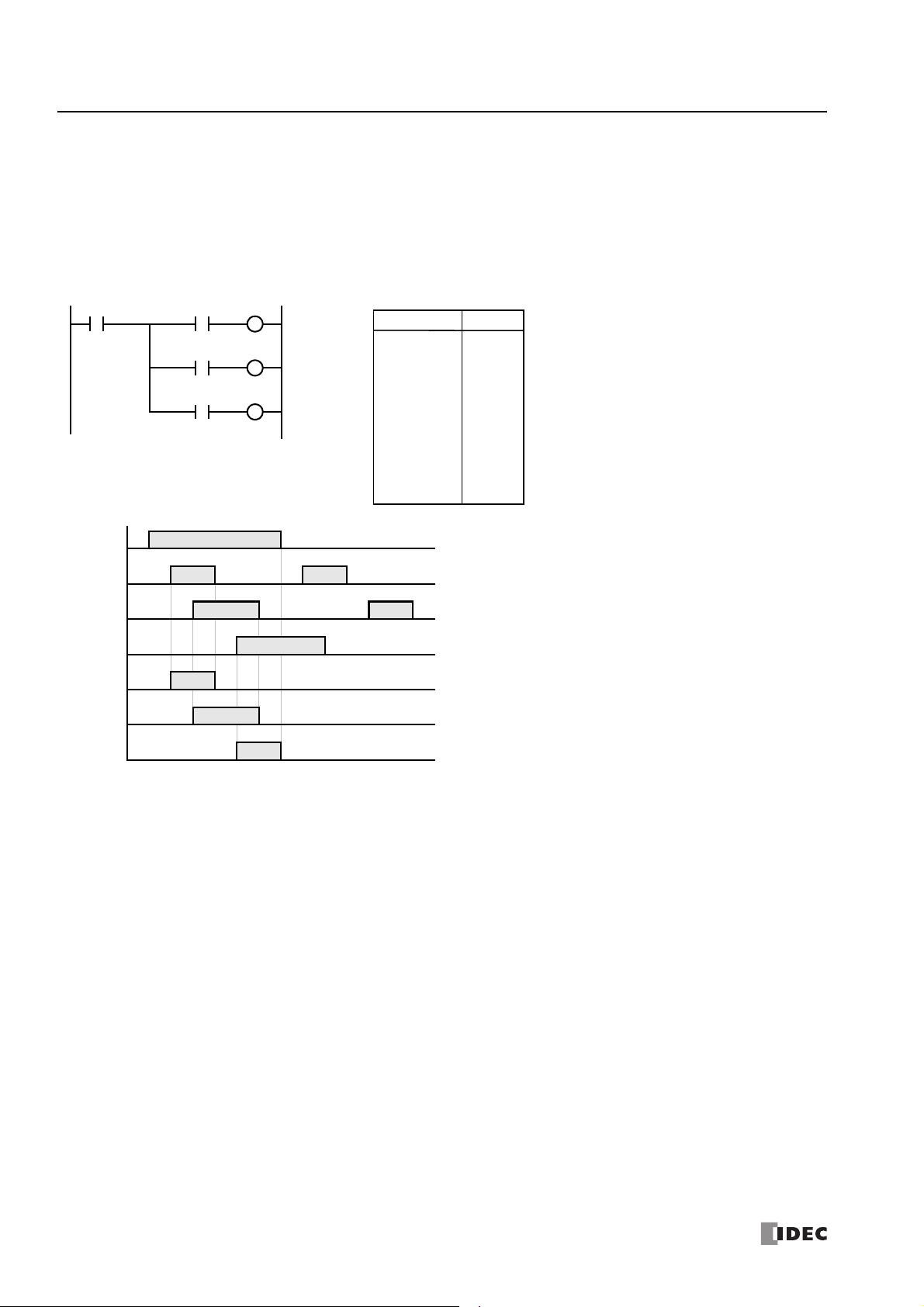
4: B
I0 I1
I2
Ladder Diagram
I0
ON
OFF
I1
ON
OFF
I2
ON
OFF
I3
ON
OFF
Timing Chart
Q1
ON
OFF
I3
Q2
ON
OFF
Q3
ON
OFF
When both inputs I0 and I1 are on, output Q1 is turned on.
When both inputs I0 and I2 are on, output Q2 is turned on.
When both inputs I0 and I3 are on, output Q3 is turned on.
BPS
BPP
BRD
Q1
Q2
Q3
LOD
BPS
AND
OUT
BRD
AND
OUT
BPP
AND
OUT
I0
I1
Q1
I2
Q2
I3
Q3
Instruction Data
Program List
ASIC INSTRUCTIONS
BPS (Bit Push), BRD (Bit Read), and BPP (Bit Pop)
The BPS (bit push) instruction is used to temporarily save the result of bit logical operation.
The BRD (bit read) instruction is used to read the result of the temporarily saved bit logical operation.
The BPP (bit pop) instruction is used to restore the result of the temporarily saved bit logical operation.
When using WindLDR, the user does not need to program the BPS, BRD, and BPP instructions. The circuit in the ladder diagram
shown below is converted into BPS, BRD, and BPP when the ladder diagram is compiled.
4-6 FC6A S
ERIES MICROSMART
LAD P
ROGRAMMING MANUAL
FC9Y-B1726
Page 77

4: B
I1
I0
T0
Ladder Diagram (TML)
TML
4
T0
I0
ON
OFF
T0
ON
OFF
I1
ON
OFF
Q0
ON
OFF
Timing Chart
4 s
Q0
LOD
TML
LOD
AND
OUT
I0
T0
4
I1
T0
Q0
Instruction Data
Program List
I1
I0
T1
Ladder Diagram (TIM)
TIM
20
T1
I0
ON
OFF
T1
ON
OFF
I1
ON
OFF
Q1
ON
OFF
Timing Chart
2 s
Q1
LOD
TIM
LOD
AND
OUT
I0
T1
20
I1
T1
Q1
Instruction Data
Program List
I1
I0
T2
Ladder Diagram (TMH)
TMH
100
T2
I0
ON
OFF
T2
ON
OFF
I1
ON
OFF
Q2
ON
OFF
Timing Chart
1 s
Q2
LOD
TMH
LOD
AND
OUT
I0
T2
100
I1
T2
Q2
Instruction Data
Program List
I1
I0
T3
Ladder Diagram (TMS)
TMS
500
T3
I0
ON
OFF
T3
ON
OFF
I1
ON
OFF
Q3
ON
OFF
Timing Chart
0.5 s
Q3
LOD
TMS
LOD
AND
OUT
I0
T3
500
I1
T3
Q3
Instruction Data
Program List
ASIC INSTRUCTIONS
TML, TIM, TMH, and TMS (Timer)
Four types of on-delay timers are available; 1-s timer TML, 100-ms timer TIM, 10-ms timer TMH, and 1-ms timer TMS. A total of
1024 on- and off-delay timers can be programmed in a user program. Each timer must be allocated to a unique number T0
through T1023.
Timer Device Address Range Increments Preset Value
TML (1-s timer) T0 to T1023 0 to 65,535 s 1 s Constant: 0 to 65,535
TIM (100-ms timer) T0 to T1023 0 to 6,553.5 s 100 ms
TMH (10-ms timer) T0 to T1023 0 to 655.35 s 10 ms
TMS (1-ms timer) T0 to T1023 0 to 65.535 s 1 ms
For details about device ranges, see "Device Addresses" on page 2-1.
To indirectly specify the value, specify it with a data register number, and specify the value of the data register in the range of 0 to 65,535.
TML (1-s Timer)
Data registers: D0 to D7999
D10000 to D55999
TIM (100-ms Timer)
TMH (10-ms Timer)
TMS (1-ms Timer)
FC6A S
ERIES MICROSMART
LAD P
ROGRAMMING MANUAL
FC9Y-B1726 4-7
Page 78

4: B
I1
Ladder Diagram
TIM
D10
T5
Q0
LOD
TIM
OUT
I1
T5
D10
Q0
Instruction Data
Note: For restrictions on ladder programming of
timer instructions, see "Restriction on Ladder
Programming" on page 4-31.
Program List
Program Processing
Actual Input
ON
OFF
Input RAM
ON
OFF
Timer Start
Minimum Error
Tie
END
1 scan time
TIM END
Tet
Program Processing
Actual Input
ON
OFF
Input RAM
ON
OFF
Timer Start
Maximum Error
END
1 scan time
TIM END
Tet
TIM
Tie
When the input turns on immediately before END processing,
Tie is almost 0. Then the timer input error is only Tet (behind
error) and is at its minimum.
When the input turns on immediately after END processing, Tie is
almost equal to one scan time. Then the timer input error is Tie +
Tet = one scan time + Tet (behind error) and is at its maximum.
Tie: Time from input turning on to END processing
Tet: Time from END processing to the timer instruction execution
ASIC INSTRUCTIONS
Timer Circuit
The preset value 0 through 65,535 can be designated using a data register D0 thorough D7999 or D10000 through D55999; then
the data of the data register becomes the preset value. Directly after the TML, TIM, TMH, or TMS instruction, the OUT, OUTN, SET,
RST, TML, TIM, TMH, TMS, TMLO, TIMO, TMHO, or TMSO instruction can be programmed.
• Countdown from the preset value is initiated when the operation result directly before the timer input is on.
• The timer output turns on when the current value (timed value) reaches 0.
• The current value returns to the preset value when the timer input is off.
• Timer preset and current values can be changed using WindLDR without downloading the entire program to the CPU again. From the
WindLDR menu bar, select Online > Monitor > Monitor, then Online > Custom > New Custom Monitor.
• If a timer preset value is changed during countdown, the timer remains unchanged for that cycle. The change will be reflected in the next
time cycle.
• If a timer preset value is changed to 0, then the timer stops operation, and the timer output is turned on immediately.
• If a current value is changed during countdown, the change becomes effective immediately.
• For data movement when changing, confirming, and clearing preset values, see "Changing, Confirming, and Clearing Preset Values for Timers
and Counters" on page 4-17. Preset values can also be changed and confirmed using the LCD screen and pushbuttons.
• WindLDR ladder diagrams show TP (timer preset value) and TC (timer current value) in advanced instruction devices.
• The timer instructions (TML, TIM, TMH, TMS) and off-delay timer instructions (TMLO, TIMO, TMHO, TMSO) cannot be used in an interrupt
program.
• If used, a user program execution error will result, turning on special internal relay M8004 and the ERR LED on the FC6A Series MicroSmart.
For details about the user program execution errors, see "User Program Execution Errors" on page 3-10.
Timer Accuracy
Timer accuracy due to software configuration depends on three factors: timer input error, timer counting error, and timeout output
error. These errors are not constant but vary with the user program and other causes.
Timer Input Error
The input status is read at the END processing and stored to the input RAM. So, an error occurs depending on the timing when the
timer input turns on in a scan cycle. The same error occurs on normal input and catch input. The timer input error shown below
does not include input delay caused by the hardware.
4-8 FC6A S
ERIES MICROSMART
LAD P
ROGRAMMING MANUAL
FC9Y-B1726
Page 79

4: B
Program Processing
Timeout Output RAM
ON
OFF
Actual Output
ON
OFF
END
1 scan time
TIM END
Tte
Ladder Diagram
I1
I1
ON
OFF
C2
ON
OFF
Timing Chart
10 s
(10-s Timer)
CNT C2
1000
M8123
Reset
Pulse
Note: Designate counter C2 used in this program as a keep type counter. See Chapter 5 "Memory Backup" in
the "FC6A Series MicroSmart All-in-One Type User’s Manual".
LODN
LOD
CNT
I1
M8123
C2
1000
Instruction Data
Program List
ASIC INSTRUCTIONS
Timer Counting Error
Every timer instruction operation is individually based on asynchronous 16-bit reference timers. Therefore, an error can occur
depending on the status of the asynchronous 16-bit timer when the timer instruction is executed. Use of a TMS (1-ms timer) is
recommended to reduce advance errors.
Maximum
Error
TML
(1-s timer)
Advance error 1,000 ms 100 ms 10 ms 1 ms
Behind error 1 scan time 1 scan time 1 scan time 1 scan time
TIM
(100-ms timer)
TMH
(10-ms timer)
TMS
(1-ms timer)
Timeout Output Error
The output RAM status is set to the actual output when the END instruction is processed. When timeout output turns from off to
on, an error occurs depending on the position where the timer instruction is programmed in the user program. The timeout output
error shown below does not include output delay caused by the hardware.
Timeout output error is equal to Tte (behind error) and can be between
0 and one scan time.
0 < Tte < 1 scan time
Tte: Time from the timer instruction execution to the END processing
Error Maximum and Minimum
Timer Counting
Error
Minimum
Error Timer Input Error
Advance error 0 (Note) 0 0 (Note) 0
Behind error Tet + Tie 0 Tte 0
Advance error 0 (Note) Increment 0 (Note) Increment – (Tet + Tte)
Maximum
Notes: Advance error does not occur at the timer input and timeout output.
Behind error
1 scan time +
Tet (1 scan time)
1 scan time Tte (1 scan time) 2 scan times + (Tet + Tte)
Tet + Tte = 1 scan time
Increment is 1 s (TML), 100 ms (TIM), 10 ms (TMH), or 1 ms (TMS).
The maximum advance error is: Increment – 1 scan time
The maximum behind error is: 3 scan times
The timer input error and timeout output error shown above do not include the input response time (behind error) and output response
time (behind error) caused by hardware.
Timeout Output
Error
Total Error
Power Failure Memory Protection
Timers TML, TIM, TMH, and TMS do not have power failure protection. To provide a timer with this protection use a counter
instruction and special internal relay M8121 (1-s clock), M8122 (100-ms clock), or M8123 (10-ms clock).
FC6A S
ERIES MICROSMART
LAD P
ROGRAMMING MANUAL
FC9Y-B1726 4-9
Page 80

4: B
I1
I0
T0
Ladder Diagram (TMLO)
TMLO4T0
I0
ON
OFF
T0
ON
OFF
I1
ON
OFF
Q0
ON
OFF
Timing Chart
4 s
Q0
LOD
TMLO
LOD
AND
OUT
I0
T0
4
I1
T0
Q0
Instruction Data
Program List
I1
I0
T1
Ladder Diagram (TIMO)
TIMO20T1
I0
ON
OFF
T1
ON
OFF
I1
ON
OFF
Q1
ON
OFF
Timing Chart
Q1
2 s
LOD
TIMO
LOD
AND
OUT
I0
T1
20
I1
T1
Q1
Instruction Data
Program List
I1
I0
T2
Ladder Diagram (TMHO)
TMHO
100
T2
I0
ON
OFF
T2
ON
OFF
I1
ON
OFF
Q2
ON
OFF
Timing Chart
1 s
Q2
LOD
TMHO
LOD
AND
OUT
I0
T2
100
I1
T2
Q2
Instruction Data
Program List
I1
I0
T3
Ladder Diagram (TMSO)
TMSO
500
T3
I0
ON
OFF
T3
ON
OFF
I1
ON
OFF
Q3
ON
OFF
Timing Chart
0.5 s
Q3
LOD
TMSO
LOD
AND
OUT
I0
T3
500
I1
T3
Q3
Instruction Data
Program List
ASIC INSTRUCTIONS
TMLO, TIMO, TMHO, and TMSO (Off-Delay Timer)
Four types of on-delay off-delay timers are available; 1-s off-delay timer TMLO, 100-ms off-delay timer TIMO, 10-ms off-delay
timer TMHO, and 1-ms off-delay timer TMSO. A total of 1024 on- and off-delay timers can be programmed in a user program. Each
timer must be allocated to a unique number T0 through T1023.
Timer Device Address Range Increments Preset Value
TMLO (1-s off-delay timer) T0 to T1023 0 to 65,535 s 1 s Constant: 0 to 65,535
TIMO (100-ms off-delay timer)
T0 to T1023 0 to 6,553.5 s 100 ms
TMHO (10-ms off-delay timer) T0 to T1023 0 to 655.35 s 10 ms
TMSO (1-ms off-delay timer) T0 to T1023 0 to 65.535 s 1 ms
For details about device ranges, see "Device Addresses" on page 2-1.
To indirectly specify the value, specify it with a data register number, and specify the value of the data register in the range of 0 to 65,535.
TMLO (1-s Off-delay Timer)
Data registers: D0 to D7999
D10000 to D55999
TIMO (100-ms Off-delay Timer)
TMHO (10-ms Off-delay Timer)
TMSO (1-ms Off-delay Timer)
4-10 FC6A S
ERIES MICROSMART
LAD P
ROGRAMMING MANUAL
FC9Y-B1726
Page 81

CNT, CDP, and CUD (Counter)
Ladder Diagram
I2
Reset Input I0
ON
OFF
Pulse Input I1
ON
OFF
Counter C0
ON
OFF
Timing Chart
Output Q0
ON
OFF
1
Input I2
• • •
C0
23456
ON
OFF
CNT C0
5
I1
Reset
Pulse
I0
• The preset value 0 through 65,535 can be designated using a data
register D0 thorough D7999 or D10000 through D55999; then the
data of the data register becomes the preset value.
• Directly after the CNT instruction, the OUT, OUTN, SET, RST, TML,
TIM, TMH, or TMS instruction can be programmed.
Q0
LOD
LOD
CNT
LOD
AND
OUT
I0
I1
C0
5
I2
C0
Q0
Instruction Data
CNT C28
D5
I1
Reset
Pulse
I0 Q0
Program List
Three types of counters are available; adding (up) counter CNT, dual-pulse reversible counter CDP, and up/down selection
reversible counter CUD. A total of 512 counters can be programmed in a user program. Each counter must be allocated to a unique
number C0 through C511.
Counter Device Address Preset Value
CNT (adding counter) C0 to C511 Constant: 0 to 65,535
CDP (dual-pulse reversible counter) C0 to C511
CUD (up/down selection reversible counter) C0 to C511
For details about device ranges, see "Device Addresses" on page 2-1.
To indirectly specify the value, specify it with a data register number, and specify the value of the data register in the range of 0 to 65,535.
CNT (Adding Counter)
When counter instructions are programmed, two addresses are required. The circuit for an adding (UP) counter must be
programmed in the following order: reset input, pulse input, the CNT instruction, and a counter number C0 through C511, followed
by a counter preset value from 0 to 65,535.
The preset value can be designated using a decimal constant or a data register. When a data register is used, the data of the data
register becomes the preset value.
4: B
ASIC INSTRUCTIONS
Data registers: D0 to D7999
D10000 to D55999
• A single counter number cannot be programmed more than once.
• While the reset input is off, the counter counts the leading edges
of pulse inputs and compares them with the preset value.
• When the current value reaches the preset value, the counter
turns output on. The output stays on until the reset input is
turned on.
• When the reset input changes from off to on, the current value is
reset.
• When the reset input is on, all pulse inputs are ignored.
• The reset input must be turned off before counting may begin.
• When power is off, the counter’s current value is held, and can
also be designated as “clear” type counters using Function Area
Settings (see Chapter 5 "Memory Backup" in the "FC6A Series
MicroSmart All-in-One Type User’s Manual".).
• Counter preset and current values can be changed using
WindLDR without downloading the entire program to the CPU
again. From the WindLDR menu bar, select Online > Monitor >
Monitor, then Online > Custom > New Custom Monitor.
Change the current value while the counter reset input is off.
• When the preset or current value is changed during counter
operation, the change becomes effective immediately.
• When power is off, the preset values that were changed are
cleared and the original preset values are loaded.
• For data movement when changing, confirming, and clearing
preset values, see "Changing, Confirming, and Clearing Preset
Values for Timers and Counters" on page 4-17. Preset values can
also be changed and confirmed using the LCD screen and
pushbuttons.
• WindLDR ladder diagrams show CP (counter preset value) and
CC (counter current value) in advanced instruction devices.
• The CNT instruction cannot be used in an interrupt program.
If used, a user program execution error will result, turning on
special internal relay M8004 and the ERR LED on the FC6A Series
MicroSmart. For details about the user program execution errors,
see "User Program Execution Errors" on page 3-10.
FC6A S
ERIES MICROSMART
LAD P
ROGRAMMING MANUAL
FC9Y-B1726 4-11
Page 82

4: B
500 500
Ladder Diagram
Preset Input I0
ON
OFF
Up Pulse I1
ON
OFF
Down Pulse I2
ON
OFF
Timing Chart
Counter C1
ON
OFF
500 501 502 501
Counter C1 Value
500 499 0 1
• • •
• • •
I0
I1
CDP C1
500
I2
Preset Input
Up Pulse
Down Pulse
I3 C1 Q1
LOD
LOD
LOD
CDP
LOD
AND
OUT
I0
I1
I2
C1
500
I3
C1
Q1
Instruction Data
Program List
CDP (Dual-Pulse Reversible Counter)
The dual-pulse reversible counter CDP has up and down pulse inputs, so the three inputs are required. The circuit for a dual-pulse
reversible counter must be programmed in the following order: preset input, up-pulse input, down-pulse input, the CDP
instruction, and a counter number C0 through C511, followed by a counter preset value from 0 to 65,535.
The preset value can be designated using a decimal constant or a data register. When a data register is used, the data of the data
register becomes the preset value.
Note: For restrictions on ladder programming of counter instructions, see "Restriction on Ladder Programming" on page 4-31.
Counter Operation after Count out
When the counter has counted out, either the current value or preset
value is changed.
Before the counter has counted out, the current value is changed to a
larger value than the preset.
The preset value is changed to 0. The counter output is turned on without regard to the current value.
When the reset input is on, the preset value is changed to 0. The counter output is not turned on.
4-12 FC6A S
ASIC INSTRUCTIONS
• A single counter number cannot be programmed more
than once.
• The preset input must be turned on initially so that the
current value returns to the preset value.
• The preset input must be turned off before counting may
begin.
• When the up pulse and down pulses are on
simultaneously, no pulse is counted.
• The counter output is on only when the current value is 0.
• After the current value reaches 0 (counting down), it
changes to 65,535 on the next count down.
• After the current value reaches 65,535 (counting up), it
changes to 0 on the next up count.
• When power is off, the counter’s current value is held, and
can also be designated as “clear” type counters using the
Function Area Settings (see Chapter 5 "Memory Backup"
in the "FC6A Series MicroSmart All-in-One Type User’s
Manual".).
• Counter preset and current values can be changed using
WindLDR without downloading the entire program to the
CPU again. From the WindLDR menu bar, select Online >
Monitor > Monitor, then Online > Custom > New
Custom Monitor. Change the current value while the
counter preset input is off.
• When the preset or current value is changed during
counter operation, the change becomes effective
immediately.
• When power is off, the changed preset values are cleared
and the original preset values are loaded.
• For data movement when changing, confirming, and
clearing preset values, see "Changing, Confirming, and
Clearing Preset Values for Timers and Counters" on page
4-17. Preset values can also be changed and confirmed
using the LCD screen and pushbuttons.
• WindLDR ladder diagrams show CP (counter preset value)
and CC (counter current value) in advanced instruction
devices. The CDP instruction cannot be used in an
interrupt program.
• If used, a user program execution error will result, turning
on special internal relay M8004 and the ERR LED on the
FC6A Series MicroSmart. For details about the user
program execution errors, see "User Program Execution
Errors" on page 3-10.
Condition Counter Output
The counter maintains the counted out status.
The counter output is turned on.
ERIES MICROSMART
LAD P
ROGRAMMING MANUAL
FC9Y-B1726
Page 83

CUD (Up/Down Selection Reversible Counter)
Ladder Diagram
I0
I1
CUD C2
500
I2
Preset Input
Pulse Input
U/D Selection
I3 C2
500 500
Preset Input I0
ON
OFF
Pulse Input I1
ON
OFF
U/D Selection
ON
OFF
Timing Chart
Counter C2
ON
OFF
500 501 502 501
Counter C2 Value
500 499 0 1
• • •
• • •
Q2
Valid Pulse Inputs
The reset or preset input has priority over the pulse input. One
scan after the reset or preset input has changed from on to off,
and the counter starts counting the pulse inputs as they change
from off to on.
Input I2
LOD
LOD
LOD
CUD
LOD
AND
OUT
I0
I1
I2
C2
500
I3
C2
Q2
Instruction Data
Reset/Preset
ON
OFF
Pulse
ON
OFF
More than one scan
time is required.
ValidInvalidValid
Program List
The up/down selection reversible counter CUD has a selection input to switch the up/down gate, so the three inputs are required.
The circuit for an up/down selection reversible counter must be programmed in the following order: preset input, pulse input, up/
down selection input, the CUD instruction, and a counter number C0 through C511, followed by a counter preset value from 0 to
65,535.
The preset value can be designated using a decimal constant or a data register. When a data register is used, the data of the data
register becomes the preset value.
Note: For restrictions on ladder programming of counter instructions, see "Restriction on Ladder Programming" on page 4-31.
4: B
ASIC INSTRUCTIONS
• A single counter number cannot be programmed more
than once.
• The preset input must be turned on initially so that the
current value returns to the preset value.
• The preset input must be turned off before counting may
begin.
• The up mode is selected when the up/down selection
input is on.
• The down mode is selected when the up/down selection
input is off.
• The counter output is on only when the current value is 0.
• After the current value reaches 0 (counting down), it
changes to 65,535 on the next count down.
• After the current value reaches 65,535 (counting up), it
changes to 0 on the next count up.
• When power is off, the counter’s current value is held, and
can also be designated as “clear” type counters using the
Function Area Settings (see Chapter 5 "Memory Backup"
in the "FC6A Series MicroSmart All-in-One Type User’s
Manual".).
• Counter preset and current values can be changed using
WindLDR without downloading the entire program to the
CPU again. From the WindLDR menu bar, select Online >
Monitor > Monitor, then Online > Custom > New
Custom Monitor. Change the current value while the
counter preset input is off.
• When the preset or current value is changed during
counter operation, the change becomes effective
immediately.
• When power is off, the changed preset values are cleared
and the original preset values are loaded.
• For data movement when changing, confirming, and
clearing preset values, see "Changing, Confirming, and
Clearing Preset Values for Timers and Counters" on page
4-17. Preset values can also be changed and confirmed
using the LCD screen and pushbuttons.
• WindLDR ladder diagrams show CP (counter preset value)
and CC (counter current value) in advanced instruction
devices. The CUD instruction cannot be used in an
interrupt program.
• If used, a user program execution error will result, turning
on special internal relay M8004 and the ERR LED on the
FC6A Series MicroSmart. For details about the user
program execution errors, see "User Program Execution
Errors" on page 3-10.
FC6A S
ERIES MICROSMART
LAD P
ROGRAMMING MANUAL
FC9Y-B1726 4-13
Page 84

4: B
Ladder Diagram
I2
Reset Input I0
ON
OFF
Pulse Input I1
ON
OFF
Counter C0
ON
OFF
Timing Chart
Output Q0
ON
OFF
99998
Input I2
• • •
C0
99999 100000
ON
OFF
CNTD C0
100000
I1
Reset
Pulse
I0
• The preset value 0 through 4,294,967,295 can be designated
using a data register D0 through D1998; then the data of the data
registers becomes the preset value.
• Directly after the CNTD instruction, the OUT, OUTN, SET, RST,
TML, TIM, TMH, TMS, TMLO, TIMO, TMHO, or TMSO instruction
can be programmed.
Q0
CNTD C28
D5
I1
Reset
Pulse
I0 Q0
LOD
LOD
CNTD
LOD
AND
OUT
Instruction Data
I0
I1
C0
100000
I2
C0
Q0
Program List
ASIC INSTRUCTIONS
CNTD, CDPD, and CUDD (Double-Word Counter)
Three types of double-word counters are available; adding (up) counter CNTD, dual-pulse reversible counter CDPD, and up/down
selection reversible counter CUDD. A total of 512 double-word counters can be programmed in a user program. Each double-word
counter uses 2 consecutive devices starting with the allocated device, which can be C0 through C510. Once used in a user
program, counters cannot be used in any other counter instructions.
Counter Device Address Preset Value
CNTD (double-word adding counter) C0 to C510 Constant: 0 to 4,294,967,295
CDPD (double-word dual-pulse reversible counter) C0 to C510
CUDD (double-word up/down selection reversible counter) C0 to C510
For details about device ranges, see "Device Addresses" on page 2-1.
The preset value can be 0 through 4,294,967,295 and designated using a constant or a data register. If a data register is designated as the preset
value, two consecutive data registers are used.
CNTD (Double-Word Adding Counter)
For a constant, specify the value in the range of 0 to 4,294,967,295.
To indirectly specify the value, specify it with a data register number, and specify the value of the data register in the range of 0 to
4,294,967,295.
The preset value can be designated using a constant or a data register. When a data register is used, the double-word data of two
consecutive data registers becomes the preset value. For 32-bit data storage setting, see Chapter 5 "32-bit Data Storage Setting"
in the "FC6A Series MicroSmart All-in-One Type User’s Manual".
Data registers: D0 to D7999
D10000 to D55999
• Double-word counter instructions use two consecutive counters,
and counters cannot be used more than once in a user program.
• While the reset input is off, the counter counts the leading edges
of pulse inputs and compares them with the preset value.
• When the current value reaches the preset value, the counter
turns output on. The output stays on until the reset input is
turned on.
• When the reset input changes from off to on, the current value is
reset.
• When the reset input is on, all pulse inputs are ignored.
• The reset input must be turned off before counting may begin.
• When power is off, the counter’s current value is held, and can
also be designated as “clear” type counters using Function Area
Settings (see Chapter 5 "Memory Backup" in the "FC6A Series
MicroSmart All-in-One Type User’s Manual".).
• Counter preset and current values can be changed using
WindLDR without downloading the entire program to the CPU
again. From the WindLDR menu bar, select Online > Monitor >
Monitor, then Online > Custom > New Custom Monitor. To
change a counter preset value, select DEC(D) in the pull-down
list box.
• When the preset or current value is changed during counter
operation, the change becomes effective immediately.
• When power is off, the changed preset values are cleared and the
original preset values are loaded.
• For data movement when changing, confirming, and clearing
preset values, see "Changing, Confirming, and Clearing Preset
Values for Timers and Counters" on page 4-17.
• WindLDR ladder diagrams show CP (counter preset value) and
CC (counter current value) in advanced instruction devices.
• The CNTD instruction cannot be used in an interrupt program.
• If used, a user program execution error will result, turning on
special internal relay M8004 and the ERR LED on the FC6A Series
MicroSmart. For details about the user program execution errors,
see "User Program Execution Errors" on page 3-10.
4-14 FC6A S
ERIES MICROSMART
LAD P
ROGRAMMING MANUAL
FC9Y-B1726
Page 85

100000 100000
Ladder Diagram
Preset Input I0
ON
OFF
Up Pulse I1
ON
OFF
Down Pulse I2
ON
OFF
Timing Chart
Counter C2
ON
OFF
100000 1 00001
Counter C2 Value
100000
01
• • •
• • •
I0
I1
CDPD C2
100000
I2
Preset Input
Up Pulse
Down Pulse
I3 C2 Q1
99999
LOD
LOD
LOD
CDPD
LOD
AND
OUT
Instruction Data
I0
I1
I2
C2
100000
I3
C2
Q1
Program List
4: B
ASIC INSTRUCTIONS
CDPD (Double-Word Dual-Pulse Reversible Counter)
The double-word dual-pulse reversible counter CDPD has up and down pulse inputs, so the three inputs are required. The circuit
for a double-word dual-pulse reversible counter must be programmed in the following order: preset input, up-pulse input, downpulse input, the CDPD instruction, and a counter number C0 through C198, followed by a counter preset value from 0 to
4,294,967,295.
The preset value can be designated using a constant or a data register. When a data register is used, the double-word data of two
consecutive data registers becomes the preset value. For 32-bit data storage setting, see Chapter 5 "32-bit Data Storage Setting"
in the "FC6A Series MicroSmart All-in-One Type User’s Manual".
• Double-word counter instructions use two consecutive
counters, and counters cannot be used more than once in
a user program.
• The preset input must be turned on initially so that the
current value returns to the preset value.
• The preset input must be turned off before counting may
begin.
• When the up and down pulses are on simultaneously, no
pulse is counted.
• The counter output is on only when the current value is 0.
• After the current value reaches 0 (counting down), it
changes to 4,294,967,295 on the next count down.
• After the current value reaches 4,294,967,295 (counting
up), it changes to 0 on the next count up.
• When power is off, the counter’s current value is held, and
can also be designated as “clear” type counters using the
Function Area Settings (see Chapter 5 "Memory Backup"
in the "FC6A Series MicroSmart All-in-One Type User’s
Manual".).
• Counter preset and current values can be changed using
WindLDR without downloading the entire program to the
CPU again. From the WindLDR menu bar, select Online >
Monitor > Monitor, then Online > Custom > New
Custom Monitor. To change a counter preset value,
select DEC(D) in the pull-down list box.
• When the preset or current value is changed during
counter operation, the change becomes effective
immediately.
• When power is off, the changed preset values are cleared
and the original preset values are loaded.
• For data movement when changing, confirming, and
clearing preset values, see "Changing, Confirming, and
Clearing Preset Values for Timers and Counters" on page
4-17.
• WindLDR ladder diagrams show CP (counter preset value)
and CC (counter current value) in advanced instruction
devices. The CNPD instruction cannot be used in an
interrupt program.
• If used, a user program execution error will result, turning
on special internal relay M8004 and the ERR LED on the
FC6A Series MicroSmart. For details about the user
program execution errors, see "User Program Execution
Errors" on page 3-10.
FC6A S
ERIES MICROSMART
LAD P
ROGRAMMING MANUAL
FC9Y-B1726 4-15
Page 86

4: B
Ladder Diagram
I0
I1
CUDD C4
100000
I2
Preset Input
Pulse Input
U/D Selection
I3 C4 Q2
Valid Pulse Inputs
The reset or preset input has priority over the pulse input. One
scan after the reset or preset input has changed from on to off,
the counter starts counting the pulse inputs as they change from
off to on.
100000 1 00000
Preset Input I0
ON
OFF
Pulse Input I1
ON
OFF
U/D Selection Input I2
ON
OFF
Timing Chart
Counter C4
ON
OFF
100000 10000 1
Counter C4 Value
100000
01
• • •
• • •
99999
LOD
LOD
LOD
CUDD
LOD
AND
OUT
Instruction Data
I0
I1
I2
C4
100000
I3
C4
Q2
Reset/Preset
ON
OFF
Pulse
ON
OFF
More than one scan
time is required.
ValidInvalidValid
Program List
ASIC INSTRUCTIONS
CUDD (Double-Word Up/Down Selection Reversible Counter)
The double-word up/down selection reversible counter CUDD has a selection input to switch the up/down gate, so the three inputs
are required. The circuit for a double-word up/down selection reversible counter must be programmed in the following order:
preset input, pulse input, up/down selection input, the CUDD instruction, and a counter number C0 through C198, followed by a
counter preset value from 0 to 4,294,967,295.
The preset value can be designated using a constant or a data register. When a data register is used, the double-word data of two
consecutive data registers becomes the preset value. For 32-bit data storage setting, see Chapter 5 "32-bit Data Storage Setting"
in the "FC6A Series MicroSmart All-in-One Type User’s Manual".
• Double-word counter instructions use two
consecutive counters, and counters cannot be used
more than once in a user program.
• The preset input must be turned on initially so that
the current value returns to the preset value.
• The preset input must be turned off before counting
may begin.
• The up mode is selected when the up/down selection
input is on.
• The down mode is selected when the up/down
selection input is off.
• The count er out put is on only when the curre nt value
is 0.
• After the current value reaches 0 (counting down), it
changes to 4,294,967,295 on the next count down.
• After the current value reaches 4,294,967,295
(counting up), it changes to 0 on the next count up.
• When power is off, the counter’s current value is
held, and can also be designated as “clear” type
counters using the Function Area Settings (see
Chapter 5 "Memory Backup" in the "FC6A Series
MicroSmart All-in-One Type User’s Manual".).
• Counter preset and current values can be changed
using WindLDR without downloading the entire
program to the CPU again. From the WindLDR menu
bar, select Online > Monitor > Monitor, then
Online > Custom > New Custom Monitor. To
change a counter preset value, select DEC(D) in the
pull-down list box.
• When the preset or current value is changed during
counter operation, the change becomes effective
immediately.
• When power is off, the changed preset values are
cleared and the original preset values are loaded.
• For data movement when changing, confirming, and
clearing preset values, see "Changing, Confirming,
and Clearing Preset Values for Timers and Counters"
on page 4-17.
• WindLDR ladder diagrams show CP (counter preset
value) and CC (counter current value) in advanced
instruction devices. The CUDD instruction cannot be
used in an interrupt program.
• If used, a user program execution error will result,
turning on special internal relay M8004 and the ERR
LED on the FC6A Series MicroSmart. For details
about the user program execution errors, see "User
Program Execution Errors" on page 3-10.
4-16 FC6A S
ERIES MICROSMART
LAD P
ROGRAMMING MANUAL
FC9Y-B1726
Page 87

4: B
Confirm Button
After pressing the Clear or
Confirm button, the display
changes to “Unchanged.”
Clear Button
WindLDR FC6A Series MicroSmart
User Program
ROM
RAM
User Program
Custom Monitor
New Preset Value
WindLDR FC6A Series MicroSmart
Confirm
User Program
ROM
RAM
User Program
Changed
Preset
Valu es
WindLDR FC6A Series MicroSmart
Clear
User Program
ROM
RAM
User Program
Original
Preset
Valu es
ASIC INSTRUCTIONS
Changing, Confirming, and Clearing Preset Values for Timers and Counters
Preset values for timers and counters can be changed by selecting Online > Monitor > Monitor, followed by Online > Custom
>
New Custom Monitor on WindLDR for transferring a new value to the FC6A Series MicroSmart RAM as described on preceding
pages. After changing the preset values temporarily, the changes can be written to the user program in the FC6A Series
MicroSmart ROM or cleared from the RAM.
When the power is off, the temporarily changed preset values in the RAM are cleared and the original preset values are loaded.
Confirm the changed preset values to store them in the ROM. The timer/counter preset values can be confirmed only when FC6A
Series MicroSmart is stopped.
To access the PLC Status dialog box from the WindLDR menu bar, select Online > Monitor > Monitor, then Online
Data movement when changing a timer/counter preset value
When changing a timer/counter preset value using
Custom Monitor on WindLDR, the new preset value is
written to the FC6A Series MicroSmart RAM. The user
program and preset values in the ROM are not
changed.
Note: The LCD screen and pushbuttons can also be used to
change preset values and confirm changed preset values.
> Status.
Data movement when confirming changed preset values
When the Confirm button is pressed before pressing
the Clear button, the changed timer/counter preset
values in the FC6A Series MicroSmart RAM are written
to the ROM.
When uploading the user program after confirming,
the user program with changed preset values is
uploaded from the FC6A Series MicroSmart ROM to
WindLDR.
Data movement when clearing changed preset values to restore original values
Changing preset values for timers and counters in the
FC6A Series MicroSmart RAM does not automatically
update preset values in the user memory, ROM. This
is useful for restoring original preset values. When
the Clear button is pressed before pressing the
Confirm button, the changed timer/counter preset
values are cleared from the RAM and the original
preset values are loaded from the ROM to the RAM.
FC6A S
ERIES MICROSMART
LAD P
ROGRAMMING MANUAL
FC9Y-B1726 4-17
Page 88

4: B
Ladder Diagram (CC=)
Ladder Diagram (CC>=)
Counter # to compare with
Preset value to compare
CC=10C2
CC>=
D15
C3
Q0
Q1
CC=
OUT
C2
10
Q0
Instruction Data
CC>=
OUT
C3
D15
Q1
Instruction Data
Program List
Program List
Ladder Diagram
Ladder Diagram
Ladder Diagram
I0I0
M0
CC=10C5 CC=
10
C5
I0
CC=
10
C5
Q0
M0 Q0 Q0
CC=
OR
OUT
C5
10
I0
Q0
Instruction Data
CC=
AND
OUT
C5
10
I0
Q0
Instruction Data
CC=
OUT
LOD
AND
OUT
C5
10
M0
I0
M0
Q0
Instruction Data
Program ListProgram List Program List
ASIC INSTRUCTIONS
CC= and CC>= (Counter Comparison)
The CC= instruction is an equivalent comparison instruction for counter current values. This instruction will constantly compare
current values to the value that has been programmed in. When the counter value equals the given value, the desired output will
be initiated.
The CC>= instruction is an equal to or greater than comparison instruction for counter current values. This instruction will
constantly compare current values to the value that has been programmed in. When the counter value is equal to or greater than
the given value, the desired output will be initiated.
When a counter comparison instruction is programmed, two addresses are required. For a constant, specify the value in the range
of 0 to 65,535.
To indirectly specify the value, specify it with a data register number, and specify the value of the data register in the range of 0 to
65,535.
The preset value can be designated using a decimal constant or a data register D0 through D1999. When a data register is used,
the data of the data register becomes the preset value.
• The CC= and CC>= instructions can be used repeatedly for different preset values.
• The comparison instructions only compare the current value. The status of the counter does not affect this function.
• The comparison instructions also serve as an implicit LOD instruction.
• The comparison instructions can be used with internal relays, which are ANDed or ORed at a separate program address.
• Like the LOD instruction, the comparison instructions can be followed by the AND and OR instructions.
4-18 FC6A S
ERIES MICROSMART
LAD P
ROGRAMMING MANUAL
FC9Y-B1726
Page 89

Examples: CC= and CC>= (Counter Comparison)
Ladder Diagram 1
Timing Chart
CC=5C2
CNT C2
10
I1
Reset
Pulse
I0
CC>=3C2
Reset Input I0
ON
OFF
Pulse Input I1
ON
OFF
C2
ON
OFF
Output Q1
ON
OFF
1
Output Q0
• • •
23456
ON
OFF
78910
Output Q0 is on when counter C2 current value is 5.
Output Q1 is turned on when counter C2 current
value reaches 3 and remains on until counter C2 is
reset.
Q0
Q1
LOD
LOD
CNT
CC=
OUT
CC³
OUT
I0
I1
C2
10
C2
5
Q0
C2
3
Q1
Instruction Data
Program List
Ladder Diagram 2
Pulse Input I2
ON
OFF
Output Q0
ON
OFF
Timing Chart
1
• • •
500 501 5022
Output Q0 is on when counter C30 current value is
500.
CC=
500
C30
CNT C30
1000
I2
Reset
Pulse
I1
Q0
LOD
LOD
CNT
CC=
OUT
Instruction Data
I1
I2
C30
1000
C30
500
Q0
Program List
Ladder Diagram 3
Pulse Input I4
ON
OFF
Output Q1
ON
OFF
Timing Chart
1
• • •
350 351 3522
Output Q1 is turned on when counter C31 current
value reaches 350 and remains on until counter C31
is reset.
CC>=
350
C31
CNT C31
500
I4
Reset
Pulse
I3
Q1
LOD
LOD
CNT
CC>=
OUT
Instruction Data
I3
I4
C31
500
C31
350
Q1
Program List
Ladder Diagram 4
Pulse Input I6
ON
OFF
C20 (100)
ON
OFF
Timing Chart
100
• • •
150 151 152101
Q2
Output Q2
ON
OFF
Output Q3
ON
OFF
• • •
Output Q3 is on when counter C20 current value is
between 100 and 149.
When the current value of C20 is between 150 and
500, Q2 is on.
CC>=
150
C20
CNT C20
500
I6
Reset
Pulse
I5
CC>=
100
C20
Q2
Q3
LOD
LOD
CNT
CC>=
OUT
CC>=
ANDN
OUT
I5
I6
C20
500
C20
150
Q2
C20
100
Q2
Q3
Instruction Data
Program List
4: B
ASIC INSTRUCTIONS
FC6A S
ERIES MICROSMART
LAD P
ROGRAMMING MANUAL
FC9Y-B1726 4-19
Page 90

4: B
Ladder Diagram (DC=)
Ladder Diagram (DC>=)
Data register # to compare with
Preset value to compare
DC=50D2
DC>=
D15
D3
Q0
Q1
DC=
OUT
D2
50
Q0
Instruction Data
DC>=
OUT
D3
D15
Q1
Instruction Data
Program List
Program List
Ladder Diagram Ladder Diagram Ladder Diagram
I0I0 M0
DC=10D5 DC=10D5
I0
DC=10D5
M0
Q0
Q0 Q0
DC=
AND
OUT
D5
10
I0
Q0
Program List
Instruction Data
DC=
OUT
LOD
AND
OUT
D5
10
M0
I0
M0
Q0
Program List
Instruction Data
DC=
OR
OUT
D5
10
I0
Q0
Program List
Instruction Data
ASIC INSTRUCTIONS
DC= and DC>= (Data Register Comparison)
The DC= instruction is an equivalent comparison instruction for data register values. This instruction will constantly compare data
register values to the value that has been programmed in. When the data register value equals the given value, the desired output
will be initiated.
The DC>= instruction is an equal to or greater than comparison instruction for data register values. This instruction will constantly
compare data register values to the value that has been programmed in. When the data register value is equal to or greater than
the given value, the desired output will be initiated.
When a data register comparison instruction is programmed, two addresses are required. For a constant, specify the value in the
range of 0 to 65,535.
To indirectly specify the value, specify it with a data register number, and specify the value of the data register in the range of 0 to
65,535.
The preset value can be designated using a decimal constant or a data register D0 through D1999. When a data register is used,
the data of the data register becomes the preset value.
For LC (Load Compare) instructions, see "LC= (Load Compare Equal To)" on page 6-8.
• The DC= and DC>= instructions can be repeated for different preset values.
• The comparison instructions also serve as an implicit LOD instruction.
• The comparison instructions can be used with internal relays, which are ANDed or ORed at a separate program address.
• Like the LOD instruction, the comparison instructions can be followed by the AND and OR instructions.
4-20 FC6A S
ERIES MICROSMART
LAD P
ROGRAMMING MANUAL
FC9Y-B1726
Page 91
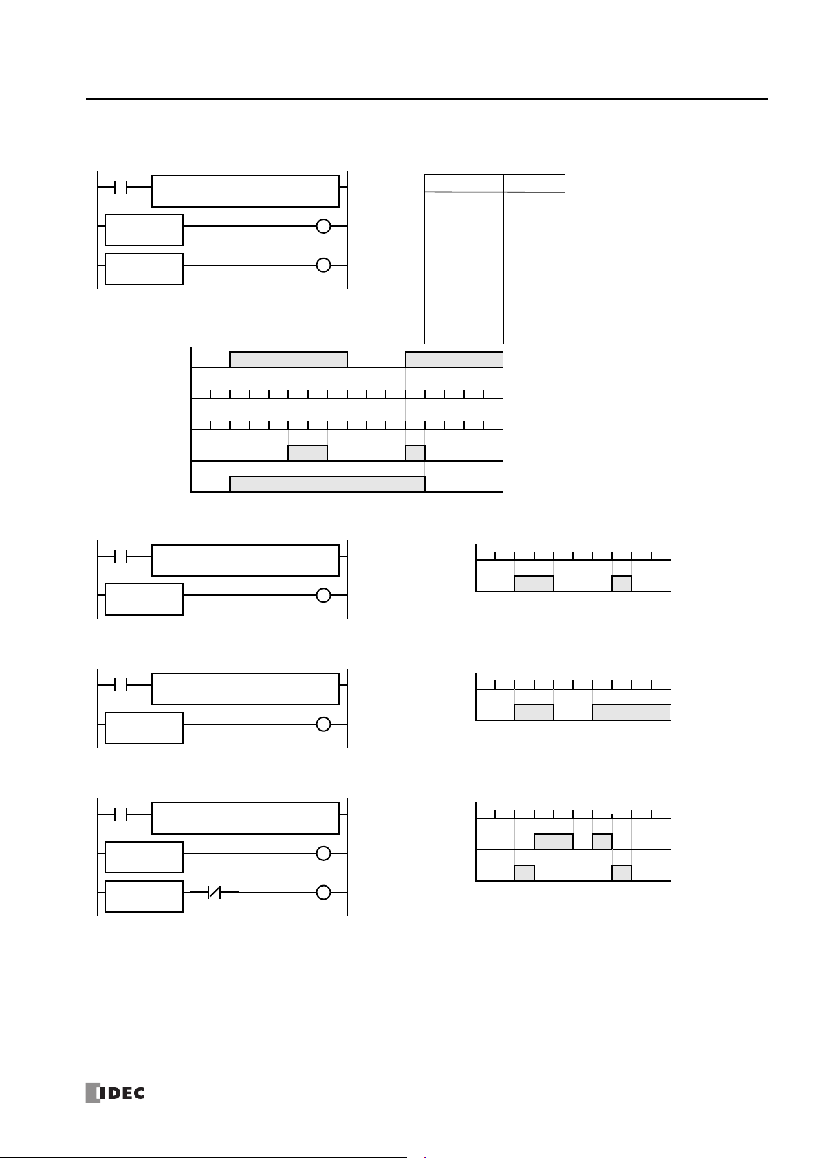
Examples: DC= and DC>= (Data Register Comparison)
Ladder Diagram 1
Timing Chart
DC=5D2
DC>=3D2
Input I1
ON
OFF
D10 Value
Output Q0
ON
OFF
Output Q1
ON
OFF
44 553 35210
I1
REPS1 –
D10
D1 –
D2
MOV(W)
10 37 22
D2 Value
04 553 35210 10 33 22
Output Q0 is on when data register D2 value is 5.
Output Q1 is on when data register D2 value is 3
or more.
Q0
Q1
LOD
MOV(W)
DC=
OUT
DC³
OUT
I1
D10 –
D2 –
D2
5
Q0
D2
3
Q1
Instruction Data
Program List
Ladder Diagram 2
Output Q0 is on when data register D30 value is 500.
DC=
500
D30
Timing Chart
Output Q0
ON
OFF
400 210 210 0 500
D30 Value
I1
REPS1 –
D50
D1 –
D30
MOV(W)
500 500 700
Q0
Ladder Diagram 3
DC>=
350
D15
I1
REPS1 –D0D1 –
D15
MOV(W)
Output Q1 is on when data register D15 value is 350 or more.
Timing Chart
Output I0
ON
OFF
200 249 200 350 390
D15 Value
355 521 600
Q1
Ladder Diagram 4
DC>=
150
D20
DC>=
100
D20
Q0
I1
REPS1 –
D100
D1 –
D20
MOV(W)
Output Q2 is on while data register D20 value is between 149 and 100.
When the value of D20 is 150 or higher, output Q0 is on.
Timing Chart
Output Q0
ON
OFF
90 150 80 160 110
D20 Value
120 180 95
Output Q2
ON
OFF
Q0
Q2
4: B
ASIC INSTRUCTIONS
FC6A S
ERIES MICROSMART
LAD P
ROGRAMMING MANUAL
FC9Y-B1726 4-21
Page 92
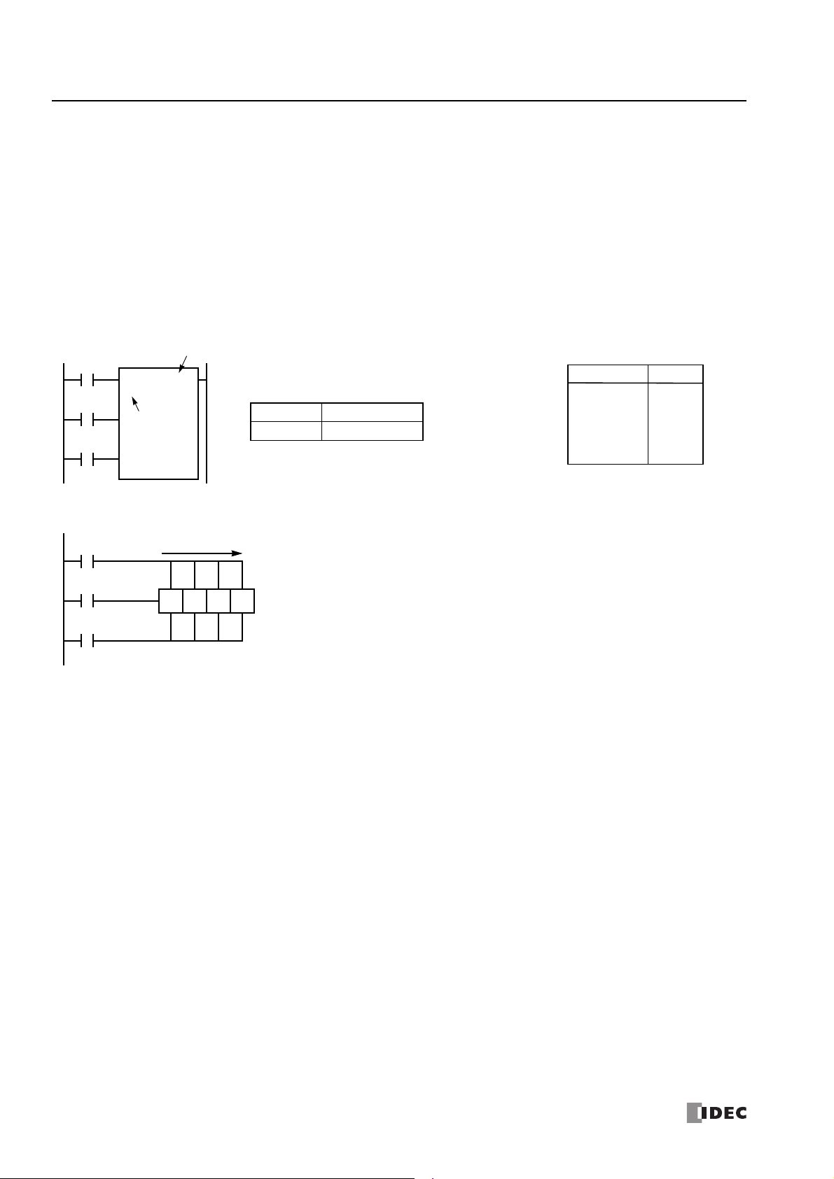
4: B
Ladder Diagram
Structural Diagram
I2
I0
R0
Reset
Data
I1
Pulse
R1 R2 R3
Shift Direction
First Bit: R0 # of Bits: 4
I0
I1
SFR R0
4
I2
Reset
Pulse
Data
First Bit
# of Bits
Structural Diagram
I2
I0
R0
Reset
Data
I1
Pulse
R1 R2 R3
Shift Direction
# of Bits: 4
LOD
LOD
LOD
SFR
I0
I1
I2
R0
4
Instruction Data
First Bit
# of Bits
R0 to R255
1 to 256
Program List
ASIC INSTRUCTIONS
SFR and SFRN (Forward and Reverse Shift Register)
FC6A Series MicroSmart have a shift register consisting of 256 bits which are allocated to R0 through R255. Any number of
available bits can be selected to form a train of bits which store on or off status. The on/off data of constituent bits is shifted in the
forward direction (forward shift register) or in the reverse direction (reverse shift register) when a pulse input is turned on.
Forward Shift Register (SFR)
When SFR instructions are programmed, two addresses are always required. The SFR instruction is entered, followed by a shift
register number selected from appropriate device addresses. The shift register number corresponds to the first, or head bit. The
number of bits is the second required address after the SFR instruction.
The SFR instruction requires three inputs. The forward shift register circuit must be programmed in the following order: reset
input, pulse input, data input, and the SFR instruction, followed by the first bit and the number of bits.
Reset Input
The reset input will cause the value of each bit of the shift register to return to zero. Initialize pulse special internal relay, M8120,
may be used to initialize the shift register at start-up.
Pulse Input
The pulse input triggers the data to shift. The shift is in the forward direction for a forward shift register and in reverse for a
reverse shift register. A data shift will occur upon the leading edge of a pulse; that is, when the pulse
been on and stays on, no data shift will occur.
Data Input
The data input is the information which is shifted into the first bit when a forward data shift occurs, or into the last bit when a
reverse data shift occurs.
Note: When power is turned off, the statuses of all shift register bits are normally cleared. It is also possible to maintain the statuses of shift
register bits by using the Function Area Settings as required. See Chapter 5 "Functions and Settings" - "Memory Backup" in the "FC6A Series
MicroSmart All-in-One Type User’s Manual".
Note: The SFR instruction cannot be used in an interrupt program. If used, a user program execution error will result, turning on special internal
relay M8004 and the ERR LED on the FC6A Series MicroSmart. For details about the user program execution errors, see "User Program Execution
Errors" on page 3-10.
Note: For restrictions on ladder programming of shift register instructions, see "Restriction on Ladder Programming" on page 4-31.
4-22 FC6A S
ERIES MICROSMART
LAD P
ROGRAMMING MANUAL
FC9Y-B1726
turns on
. If the pulse has
Page 93

4: B
Reset Input I0
ON
OFF
Pulse Input I1
ON
OFF
Data Input I2
ON
OFF
Timing Chart
R1/Q1
ON
OFF
One or more scans are required
R0/Q0
ON
OFF
R3/Q3
ON
OFF
R2/Q2
ON
OFF
Ladder Diagram
I0
I1
SFR R0
4
I2
Reset
Pulse
Data
R0
R1
R2
R3
Q0
Q1
Q2
Q3
LOD
LOD
LOD
SFR
LOD
OUT
LOD
OUT
LOD
OUT
LOD
OUT
I0
I1
I2
R0
4
R0
Q0
R1
Q1
R2
Q2
R3
Q3
Instruction Data
Program List
Ladder Diagram
I1
I2
SFR R0
4
I3
Reset
Pulse
Data
R0
R1
Q0
Q1
Q3
LOD
LOD
LOD
SFR
OUT
LOD
OUT
LOD
OUT
I1
I2
I3
R0
4
Q3
R0
Q0
R1
Q1
Instruction Data
Program List
I1
I0 R0
S
R3
R
ASIC INSTRUCTIONS
Setting and Resetting Shift Register Bits
• The last bit status output can be programmed directly after the SFR
instruction. In this example, the status of bit R3 is read to output Q3.
• Each bit can be loaded using the LOD R# instruction.
FC6A S
ERIES MICROSMART
• Any shift register bit can be turned on using the SET instruction.
• Any shift register bit can be turned off using the RST instruction.
• The SET or RST instruction is actuated by any input condition.
LAD P
ROGRAMMING MANUAL
FC9Y-B1726 4-23
Page 94

4: B
Ladder Diagram
I0
I1
SFRN R20
7
I2
Reset
Pulse
Data
R21
Last Bit
# of Bits
R23
R25
Q0
Q1
Q3
Q2
Last Bit
# of Bits
R0 to R255
1 to 256
LOD
LOD
LOD
SFRN
OUT
LOD
OUT
LOD
OUT
LOD
OUT
I0
I1
I2
R20
7
Q0
R21
Q1
R23
Q2
R25
Q3
Instruction Data
Program List
Structural Diagram
I2
I0
R20
Reset
Data
I1
Pulse
R21 R22 R23
Shift Direction
Last Bit: R20 # of Bits: 7
R24 R25 R26
ASIC INSTRUCTIONS
Reverse Shift Register (SFRN)
For reverse shifting, use the SFRN instruction. When SFRN instructions are programmed, two addresses are always required. The
SFRN instructions are entered, followed by a shift register number selected from appropriate device addresses. The shift register
number corresponds to the lowest bit number in a string. The number of bits is the second required address after the SFRN
instructions.
The SFRN instruction requires three inputs. The reverse shift register circuit must be programmed in the following order: reset
input, pulse input, data input, and the SFRN instruction, followed by the last bit and the number of bits.
• The last bit status output can be programmed directly after the SFRN instruction. In this example, the status of bit R20 is read to output Q0.
• Each bit can be loaded using the LOD R# instructions.
• For details of reset, pulse, and data inputs, see "Forward Shift Register (SFR)" on page 4-22.
Note: Output is initiated only for those bits highlighted in bold print.
Note: When power is turned off, the st atuses of all shift register bits are norm ally cleared. It is also possible to maintain the statuses of shift register
bits by using the Function Area Settings as required. See Chapter 5 "Functions and Settings" - "Memory Backup" in the "FC6A Series MicroSmart Allin-One Type User’s Manual".
Note: The SFRN instruction cannot be used in an interrupt program. If used, a user program execution error will result, turning on special internal
relay M8004 and the ERR LED on the FC6A Series MicroSmart. For details about the user program execution errors, see "User Program Execution
Errors" on page 3-10.
Note: For restrictions on ladder programming of shift register instructions, see "Restriction on Ladder Programming" on page 4-31.
4-24 FC6A S
ERIES MICROSMART
LAD P
ROGRAMMING MANUAL
FC9Y-B1726
Page 95

4: B
Structural Diagram
I3
I1
R22
Reset
Data
I2
Pulse
R23 R24 R25
Forward Shifti ng
Last Bit: R22 # of Bits: 6
R26 R27
Note: Output is initiated only for those bits highlighted in bold print.
I4
I6
I5
Reset
Data
Pulse
First Bit: R22 # of Bits: 6
Reverse Shifting
Ladder Diagram
I1
I2
SFR R22
6
I3
Reset
Pulse
Data
I4
I5
SFRN R22
6
I6
Reset
Pulse
Data
R23
R24
R26
Q0
Q2
Q1
LOD
LOD
LOD
SFR
LOD
LOD
LOD
SFRN
LOD
OUT
LOD
OUT
LOD
OUT
I1
I2
I3
R22
6
I4
I5
I6
R22
6
R23
Q0
R24
Q1
R26
Q2
Instruction Data
Program List
ASIC INSTRUCTIONS
Bidirectional Shift Register
A bidirectional shift register can be created by first programming the SFR instruction as detailed in the "Forward Shift Register
(SFR)" on page 4-22. Next, the SFRN instruction is programed as detailed in the "Reverse Shift Register (SFRN)" on page 4-24.
FC6A S
ERIES MICROSMART
LAD P
ROGRAMMING MANUAL
FC9Y-B1726 4-25
Page 96

4: B
I0
I0
Ladder Diagram
SOTU
SOTD
Q0
Q1
LOD
SOTU
OUT
LOD
SOTD
OUT
I0
Q0
I0
Q1
Instruction Data
Program List
Input I0
ON
OFF
Output Q0
ON
OFF
Output Q1
ON
OFF
Timing Chart
T
T T
T
I2
I1
Ladder Diagram
Input I1
ON
OFF
SOTU Output M1
ON
OFF
SOTD Output M2
ON
OFF
Timing Chart
MCS
SOTD
MCR
No Output No Output
I2
SOTU
Input I2
ON
OFF
M1
M2
ASIC INSTRUCTIONS
SOTU and SOTD (Single Output Up and Down)
The SOTU instruction “looks for” the transition of a given input from off to on. The SOTD instruction looks for the transition of a
given input from on to off. When this transition occurs, the desired output will turn on for the length of one scan. The SOTU or
SOTD instruction converts an input signal to a “one-shot” pulse signal.
A total of 1,024 SOTU and SOTD instructions can be used in a user program.
If operation is started while the given input is already on, the SOTU output will not turn on. The transition from off to on is what
triggers the SOTU instruction.
The SOTU or SOTD instructions cannot be used in an interrupt program.
If used, a user program execution error will result, turning on special internal relay M8004 and the ERR LED on the FC6A Series
MicroSmart. For details about the user program execution errors, see "User Program Execution Errors" on page 3-10.
When a CPU relay is defined as the SOTU or SOTD output, it may not operate if the scan time is not compatible with relay
requirements.
Note: For restrictions on ladder programming of SOTU and SOTD instructions, see "Restriction on Ladder Programming" on page 4-31.
Note: “T” equals one scan time (one-shot pulse).
There is a special case when the SOTU and SOTD instructions are used between the MCS and MCR instructions (see "MCS and
MCR (Master Control Set and Reset)" on page 4-27). If input I2 to the SOTU instruction turns on while input I1 to the MCS
instruction is on, then the SOTU output turns on. If input I2 to the SOTD instruction turns off while input I1 is on, then the SOTD
output turns on. If input I1 turns on while input I2 is on, then the SOTU output turns on. However, if input I1 turns off while input
I2 is on, then the SOTD output does not turn on as shown below.
4-26 FC6A S
ERIES MICROSMART
LAD P
ROGRAMMING MANUAL
FC9Y-B1726
Page 97

4: B
Ladder Diagram
I0
I1
Input I0
ON
OFF
Input I1
ON
OFF
Output Q0
ON
OFF
Timing Chart
MCS
MCR
When input I0 is off, MCS is executed so that the subsequent input is forced off.
When input I0 is on, MCS is not executed so that the following program is
executed according to the actual input statuses.
Q0
LOD
MCS
LOD
OUT
MCR
I0
I1
Q0
Instruction Data
Program List
ASIC INSTRUCTIONS
MCS and MCR (Master Control Set and Reset)
The MCS (master control set) instruction is usually used in combination with the MCR (master control reset) instruction. The MCS
instruction can also be used with the END instruction, instead of the MCR instruction.
When the input preceding the MCS instruction is off, the MCS is executed so that all inputs to the portion between the MCS and the
MCR are forced off. When the input preceding the MCS instruction is on, the MCS is not executed so that the program following it
is executed according to the actual input statuses.
When the input condition to the MCS instruction is off and the MCS is executed, other instructions between the MCS and MCR are
executed as follows:
Instruction Status
SOTU Rising edges (ON pulses) are not detected.
SOTD Falling edges (OFF pulses) are not detected.
OUT All are turned off.
OUTN All are turned on.
SET and RST All are held in current status.
TML, TIM, TMH, and TMS
CNT, CDP, and CUD
SFR and SFRN
Current values are reset to zero.
Timeout statuses are turned off.
Current values are held.
Pulse inputs are turned off.
Countout statuses are turned off.
Shift register bit statuses are held.
Pulse inputs are turned off.
The output from the last bit is turned off.
Input conditions cannot be set for the MCR instruction.
More than one MCS instruction can be used with one MCR instruction.
Corresponding MCS/MCR instructions cannot be nested within another pair of corresponding MCS/MCR instructions.
FC6A S
ERIES MICROSMART
LAD P
ROGRAMMING MANUAL
FC9Y-B1726 4-27
Page 98
4: B
Ladder Diagram
I1
I2
I3
I4
I5
I6
MCS
MCR
MCS
MCS
Q2
Q0
Q1
LOD
MCS
LOD
OUT
LOD
MCS
LOD
OUT
LOD
MCS
LOD
OUT
MCR
I1
I2
Q0
I3
I4
Q1
I5
I6
Q2
Instruction Data
Program List
Ladder Diagram
I1
MCS
MCR
Input I1
ON
OFF
Counter Pulse Input
ON
OFF
Shift Register Pulse Input
ON
OFF
Timing Chart
Input I2
ON
OFF
When input I1 is on, the MCS is not executed so that the counter and shift register are executed according
to the actual status of subsequent inputs I2 through I4.
When input I1 is off, the MCS is executed so that subsequent inputs I2 through I4 are forced off.
When input I1 is turned on while input I2 is on, the counter and shift register pulse inputs are turned on as
shown below.
CNT C2
10
I2
Reset
Pulse
I3
I3
I2
SFR R0
4
I4
Reset
Pulse
Data
ASIC INSTRUCTIONS
Multiple Usage of MCS instructions
This master control circuit will give priority to I1, I3, and I5, in that order.
When input I1 is off, the first MCS is executed so that subsequent inputs I2 through I6 are forced off.
When input I1 is on, the first MCS is not executed so that the following program is executed according to the actual input statuses
of I2 through I6.
When I1 is on and I3 is off, the second MCS is executed so that subsequent inputs I4 through I6 are forced off.
When both I1 and I3 are on, the first and second MCSs are not executed so that the following program is executed according to
the actual input statuses of I4 through I6.
Counter and Shift Register in Master Control Circuit
4-28 FC6A S
ERIES MICROSMART
LAD P
ROGRAMMING MANUAL
FC9Y-B1726
Page 99

4: B
Ladder Diagram
I0
I1
Input I0
ON
OFF
Input I1
ON
OFF
Output Q0
ON
OFF
Timing Chart
JMP
JEND
When input I0 is on, JMP is executed so that the subsequent output
status is held.
When input I0 is off, JMP is not executed so that the following program is
executed according to the actual input statuses.
Q0
LOD
JMP
LOD
OUT
JEND
I0
I1
Q0
Instruction Data
Program List
ASIC INSTRUCTIONS
JMP (Jump) and JEND (Jump End)
The JMP (jump) instruction is usually used in combination with the JEND (jump end) instruction. At the end of a program, the JMP
instruction can also be used with the END instruction, instead of the JEND instruction.
These instructions are used to proceed through the portion of the program between the JMP and the JEND
This is similar to the MCS/MCR instructions, except that the portion of the program between the MCS and MCR instruction
executed.
When the operation result immediately before the JMP instruction is on, the JMP is valid and the program is
the operation result immediately before the JMP instruction is off, the JMP is invalid and the program is executed.
When the input condition to the JMP instruction is on and the JMP is executed, other instructions between the JMP and JEND are
executed as follows:
Instruction Status
SOTU Rising edges (ON pulses) are not detected.
SOTD Falling edges (OFF pulses) are not detected.
OUT and OUTN All are held in current status.
SET and RST All are held in current status.
TML, TIM, TMH, and TMS
CNT, CDP, and CUD
SFR and SFRN
Current values are held.
Timeout statuses are held.
Current values are held.
Pulse inputs are turned off.
Countout statuses are held.
Shift register bit statuses are held.
Pulse inputs are turned off.
The output from the last bit is held.
without
processing.
not
executed. When
is
Input conditions cannot be set for the JEND instruction.
More than one JMP instruction can be used with one JEND instruction.
Corresponding JMP/JEND instructions cannot be nested within another pair of corresponding JMP/JEND instructions.
FC6A S
ERIES MICROSMART
LAD P
ROGRAMMING MANUAL
FC9Y-B1726 4-29
Page 100
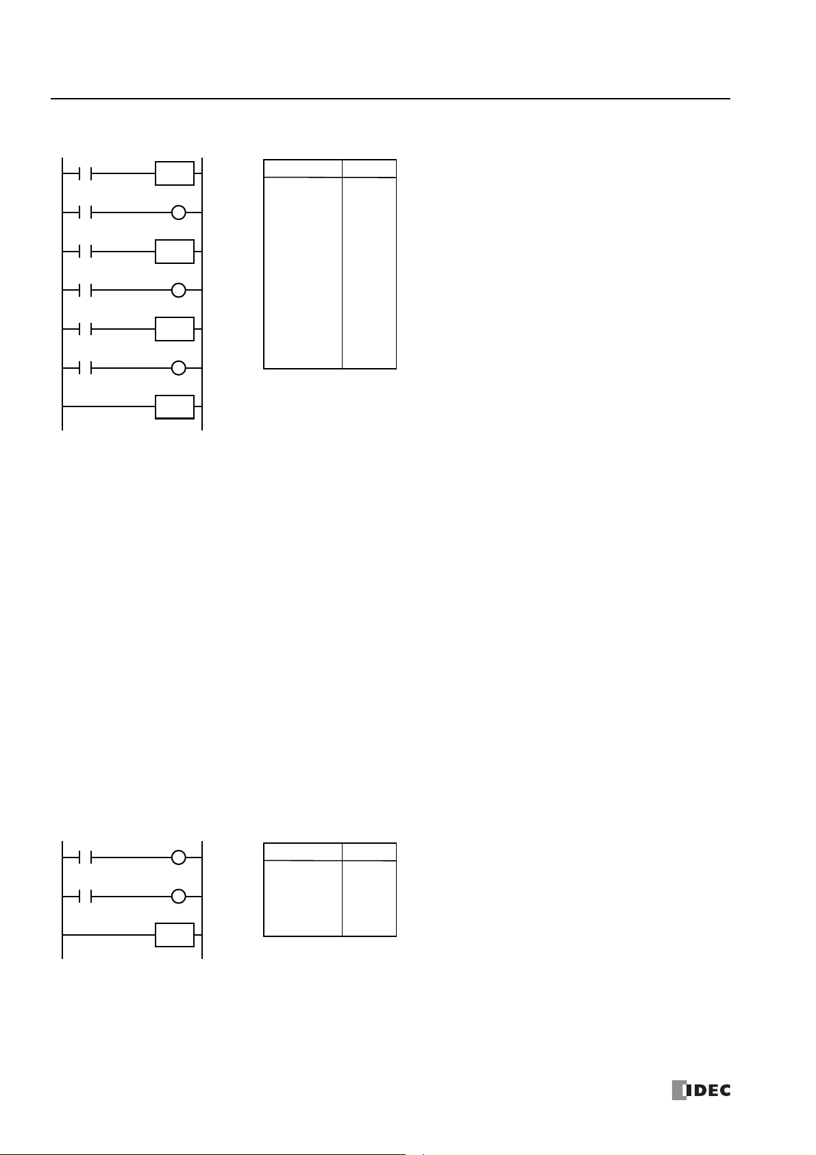
4: B
Ladder Diagram
I1
I2
I3
I4
I5
I6
JMP
JEND
JMP
JMP
This jump circuit will give priority to I1, I3, and I5, in that order.
When input I1 is on, the first JMP is executed so that subsequent output statuses of Q0 through Q2 are held.
When input I1 is off, the first JMP is not executed so that the following program is executed according to the actual input statuses of I2 through
I6.
When I1 is off and I3 is on, the second JMP is executed so that subsequent output statuses of Q1 and Q2 are held.
When both I1 and I3 are off, the first and second JMPs are not executed so that the following program is executed according to the actual input
statuses of I4 through I6.
Q2
Q0
Q1
LOD
JMP
LOD
OUT
LOD
JMP
LOD
OUT
LOD
JMP
LOD
OUT
JEND
I1
I2
Q0
I3
I4
Q1
I5
I6
Q2
Instruction Data
Program List
Ladder Diagram
END
Q1
I0
I1
Q0
LOD
OUT
LOD
OUT
END
I0
Q0
I1
Q1
Instruction Data
Program List
ASIC INSTRUCTIONS
END
The END instruction is always required at the end of a program; however, it is not necessary to program the END instruction after
the last programmed instruction. WindLDR automatically appends the END instruction at the end of a program.
A
scan
to as one
instruction is found.
During the scan time, program instructions are processed sequentially. This is why the output instruction closest to the END
instruction has priority over a previous instruction for the same output. No output is initiated until all logic within a scan is
processed.
Output occurs simultaneously, and this is the first part of the END instruction execution. The second part of the END instruction
execution is to monitor all inputs, also done simultaneously. Then program instructions are ready to be processed sequentially
once again.
is the execution of all instructions from address zero to the END instruction. The time required for this execution is referred
scan time
. The scan time varies with respect to program length, which corresponds to the address where the END
4-30 FC6A S
ERIES MICROSMART
LAD P
ROGRAMMING MANUAL
FC9Y-B1726
 Loading...