PA7572 PEEL Array™
Programmable Electrically Erasable Logic Array
Commercial/Industrial
Versatile Logic Array Architecture
- 24 I/Os, 14 inputs, 60 registers/latches
- Up to 72 logic cell output functions
- PLA structure with true product-ter m sharing
- Logic functions and registers can be I/O-buried
High-Speed Commercial and Industrial Versions
- As fast as 13ns/20ns (tpdi/tpdx), 66.6MHz (f
-
Industrial grade available for 4.5 to 5.5V V
)
MAX
and -40
CC
to +85 °C temperatures
Ideal for Combinatorial, Synchronous and
Asynchronous Logic Applications
- Integration of multiple PLDs and random logic
- Buried counters, complex state-machines
- Comparators, decoders, other wide-gate functions
General Description
The PA7572 is a m ember of the Pr ogramm able Electr icall y
Erasable Logic (PEEL™) Array family based on ICT’s
CMOS EEPROM technology. PEEL™ Arrays free
designers from the limitations of ordinary PLDs by
providing the arc hitectural flexibilit y and speed needed for
today’s programm able logic designs. T he PA7572 offers a
versatile logic ar ray architecture with 2 4 I/O pins, 14 input
pins and 60 registers/ latche s ( 24 buried logic cells, 12 input
registers/latches, 24 buried I/O registers/latches). Its logic
array implements 100 sum-of-products logic functions
divided into two groups each serving 12 log ic cells. Each
group shares half (60) of the 120 product-terms available.
CMOS Electrically Erasable Technology
-
Reprogrammable in 40-pin DIP,
44-pin PLCC and TQFP packages
Flexible Logic Cell
- Up to 3 output functions per logic cell
- D,T and JK registers with special features
- Independent or global clocks, resets, presets,
clock polarity and output enables
- Sum-of-products logic for output enables
Development and Programmer Support
- ICT PLACE Development Software
- Fitters for ABEL, CUPL and other software
- Programming support by popular third-party
programmers
The PA7572’s logic and I/O cells (LCCs, IOCs) are
extremely flexible with u p to three output functi ons per cell
(a total of 72 for all 24 log ic c ells ) . Cel ls ar e configurable as
D, T, and JK registers with independent or global clocks,
resets, presets, cloc k polarity, and other features, m aking
the PA7572 suitable for a variety of combinatorial,
synchronous and asynchronous logic applications. The
PA7572 supports spee ds as fast as 13ns/20ns (tpdi/tpdx )
and 66.6MHz (f
) at moderate power consumption
MAX
140mA (100mA typical). Packaging includes 40-pin DIP
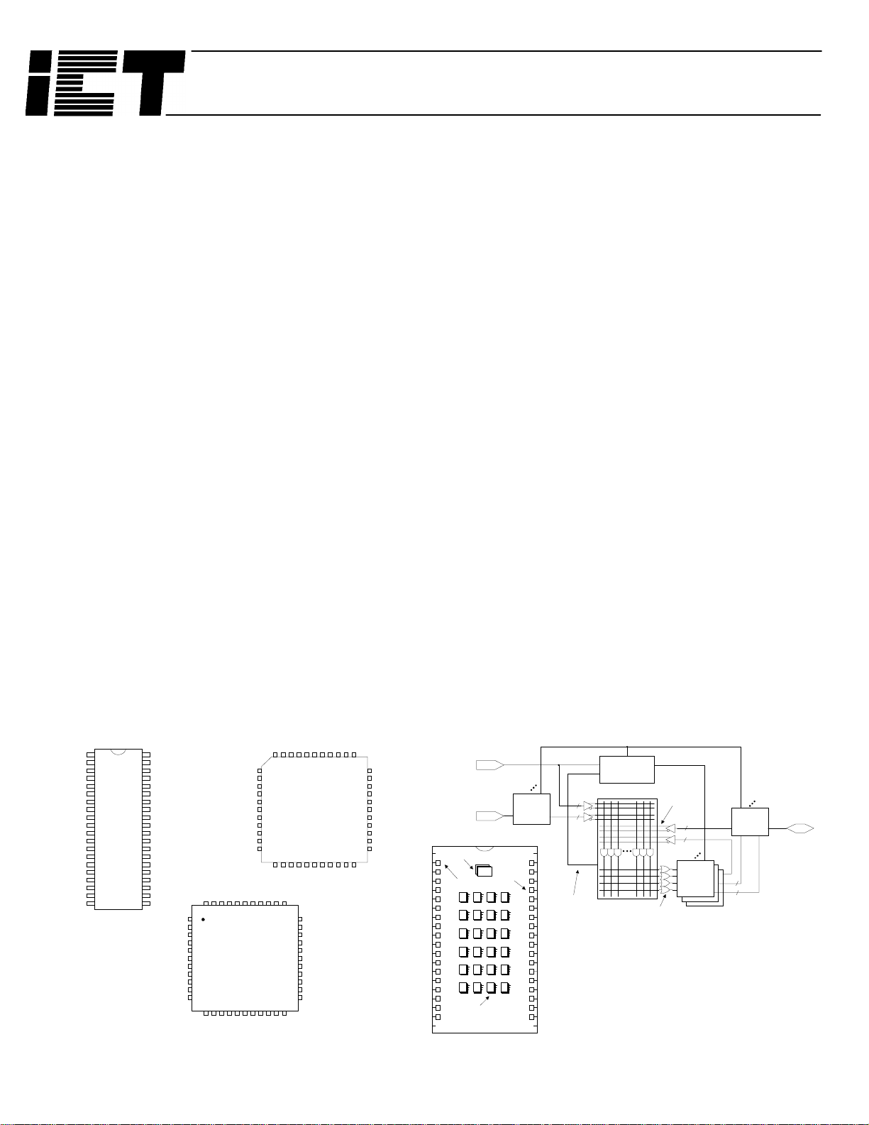
and 44-pin PLCC (see Figure 1). ICT and popular thirdparty development tool manufacturers provide
development and programming support for the PA7572.
Figure 1. Pin Configuration
I/CL K 1
GND
I/O
I/O
I/O
I/O
I/O
I/O
I/O
I/O
I/O
I/O
I/O
I/O
DIP (600 mil)
1
I
2
I
3
I
4
5
6
7
8
9
10
11
12
13
14
15
16
I
17
I
18
I
19
20
40
39
38
37
36
35
34
33
32
31
30
29
28
27
26
25
24
23
22
21
TQFP
VCC
I
I
I
I/O
I/O
I/O
I/O
I/O
I/O
I/O
I/O
I/O
I/O
I/O
I/O
I
I
I
I/CL K 2
GND
I/O
I/O
I/O
I/O
I/O
I/O
I/O
I/O
I/O
I/O
1
2
3
4
5
6
7
8
9
10
11
12
I/O43I
44
13I14I15I16
I/O
42I41I40
PLCC
GND
I/CL K 1
39
GND17GND
I/O
I/O
I/O
I/O
I/O
I/O
I/O
I/O
I/O
I/O
VCC38VCC37I36I
18
19I20I21I22
I/CL K 2
7
8
9
10
11
12
13
14
15
16
17
I/O5I
6
18
19I20I21I22
I/O
35I34
4I3I2
I/O
33
32
31
30
29
28
27
26
25
24
23
I/O
GND
I/O
I/O
I/O
I/O
I/O
I/O
I/O
I/O
I/O
I/O
I/CL K 1
GND23GND
VCC44VCC43I42I
1
24
25I26I27I28
I/CL K 2
08-15-001A
41I40
Figure 2. Block Diagram
I/O
GND
39
I/O
38
I/O
37
I/O
36
I/O
35
I/O
34
I/O
33
I/O
32
I/O
31
I/O
30
I/O
29
I/O
I/CL K
I
I
I
I/O
I/O
I/O
I/O
I/O
I/O
I/O
I/O
I/O
I/O
I/O
I/O
I
I
I
2 Input/
Global Clock Pins
12 Input Pins
Global Cells
Input Cells
Logic Control Cells
PA7572
I/O C e l ls
Input
Cells
(INC)
VCC
I
I
I
I/O
I/O
I/O
I/O
I/O
I/O
I/O
I/O
I/O
I/O
I/O
I/O
I
I
I
I/CL K 2GND
2
12
4 sum terms
5 product term s
for Global Cells
Global
Cells
Logic
Array
124 (62X2)
Array Inputs
true and
complement
A
B
C
D
96 sum terms
(four per LC C )
I/O
24
24
Logic
Control
Cells
(LCC)
Cells
(IOC)
Buried
logic
24
24
24 Logic Control Cells
up to 3 output functions per cell
(72 total output functions
possible)
08-15-002A
24 I/O Pins
Logic
func tio ns
to I/O cells
1 04-02-050A

Commercial/Industrial
Inside the Logic Array
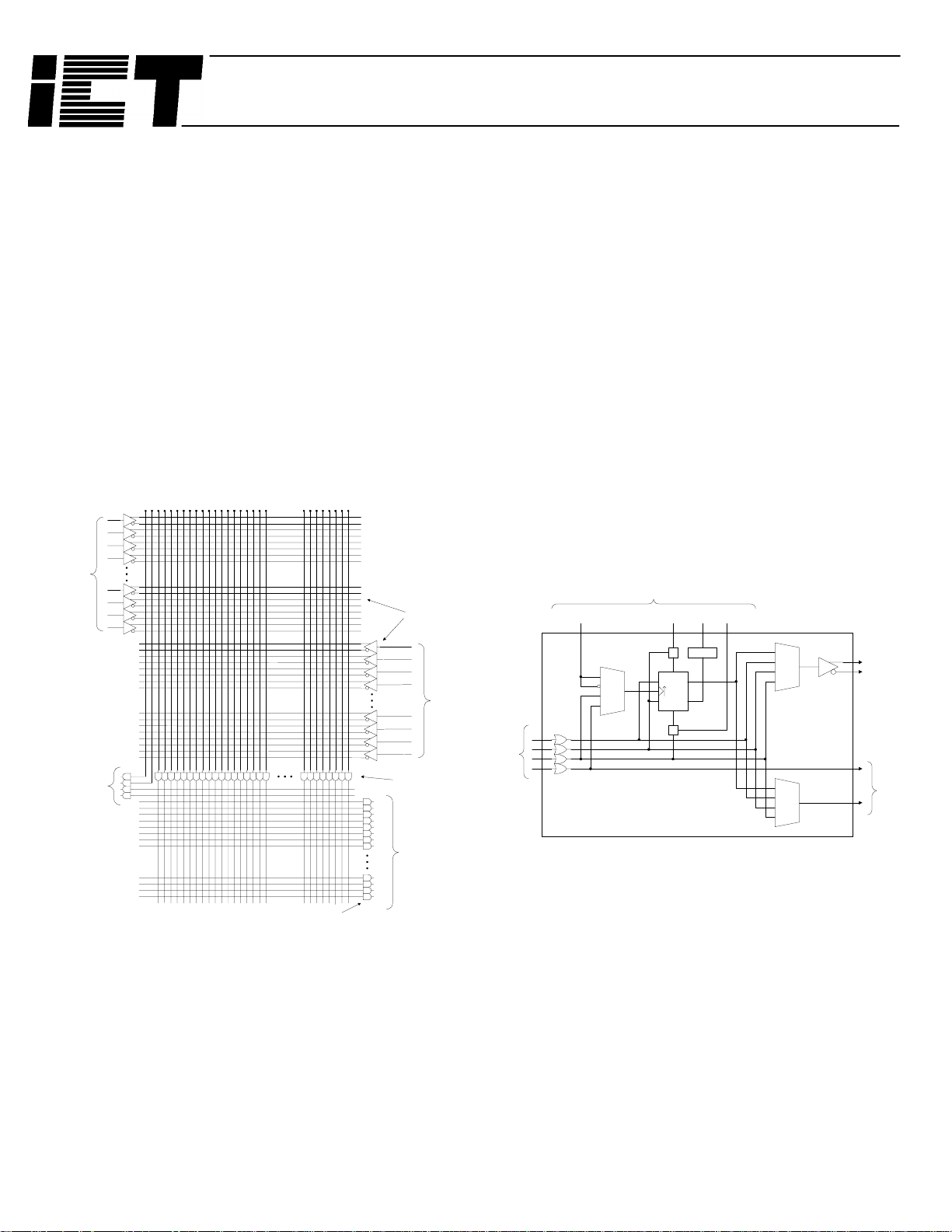
The heart of the P EEL™ Array architecture is based on a
logic array structur e s imilar to that of a PLA (programmable
AND, programmable OR). The logic array implements all
logic functions and provi des interconnection and contr ol of
the cells. In the PA7572 PEEL™ Array, 62 inputs are
available into the arra y from the I/O cells, inputs cells and
input/global-clock pins.
All inputs provide b oth true and c omplem ent signa ls, which
can be programm ed to any product term in the array. T he
PA7572 PEEL™ Arrays contains 124 product terms. All
product terms ( with the ex ception of c ertain ones f ed t o the
global cells) can be progr ammabl y connected to any of the
sum-terms of the logic control cells (four sum-terms per
logic control cell). Product-terms and sum-terms are also
routed to the global cells for control purposes. Figure 3
shows a detailed view of the logic array structure.
From
IO Cells
(IOC,INC,
I/CLK)
62 Array In puts
products functions pro vided to the logic c ells can be used f or
clocks, resets, presets and output enables instead of just
simple product-term control.
The PEEL™ logic array can also implement logic functions
with many product terms within a single-level delay. For
example a 16-bit c omparator ne eds 32 shared product term s
to implement 16 exclusive-OR functions. The PEEL™ logic
array easily handles this in a single level delay. Other
PLDs/CPLDs either run out of product-terms or require
expanders or additional logic levels that often slow
performance and skew timing.
Logic Control Cell (LCC)
Logic Control Cells (LCC) a re us ed t o a ll oc ate and c on trol th e
logic functions created in the logic array. Each L CC has four
primary inputs and thre e outputs . T he inputs t o each LCC are
complete sum-of - produc t logic f unc tions f rom the array, which
can be used to implem ent combinatoria l and sequential l ogic
functions, and to control LCC registers and I/O cell output
enables.
From G lobal Cell
Preset Reset
System C lock
RegType
From
Logic
Control
Cells
(LCC)
To
Global
Cells
PA7572 Logic Array
Figure 3. PA7572 Logic Array
True Product-Term Sharing
100 Sum Terms
125 Product
Terms
To
Logic Control
Cells
(LCC)
08-15-003A
The PEEL™ logic arra y provides several advantages over
common PLD logic arra ys. First, it allows for true pro ductterm sharing, not simply product-term steering, as commonly found in other CP LD s . Pr oduct ter m sharing ensures
that product-terms are used where they are needed and
not left unutilized or duplicated. Secondly, the sum-of-
From
Array
On/Off
P
Q
D,T,J
MUX
A
B
C
D
K
REG
R
MUX
MUX
08-15-004A
Figure 4. Logic Control Cell Block Diagram
As shown in Figure 4, the LCC is made up of three signal
routing multiplexer s and a versatile reg ister with s ynchronous
or asynchronous D, T , or JK registers (c locked-SR registers,
which are a subset of JK, are also possible). See Figure 5.
EEPROM memory cells are used for programming the
desired configuration. Four sum-of-product logic functions
(SUM terms A, B, C and D) are f ed into each LCC from the
logic array. Each SUM term can be selectively used for
multiple functions as listed below.
To
Array
To
I/O
Cell
2 04-02-050A

Commercial/Industrial
Sum-A = D, T, J or Sum-A
Sum-B = Preset, K or Sum-B
Sum-C = Reset, Clock, Sum-C
Sum-D = Clock, Output Enable, Sum-D
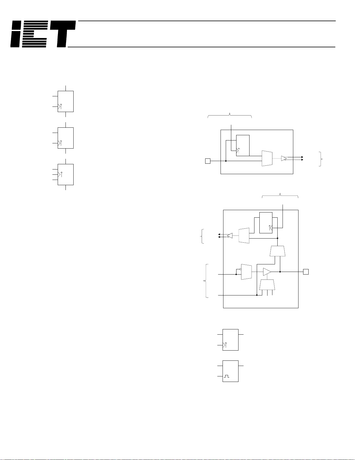
D Register
Q = D after clocked
P
D
Q
Best for storage, simple counters,
shifters and state machines with
R
few hold (loop) conditions.
T Register
Q toggles when T = 1
P
Q
T
J
K
Q holds when T = 0
Best for wide binary counters (saves
R
product terms) and state machines
with many hold (loop) conditions.
JK Register
Q toggles when J/K = 1/1
P
Q
Q holds when J/K = 0/0
Q = 1 w h e n J/K = 1/0
Q = 0 w h e n J/K = 0/1
R
Combines features of both D and T
registers.
08-15-005A
Figure 5. LCC Register Types
SUM-A can serve as the D, T, or J input of the reg is ter or a
combinatorial pat h. SUM-B can s erve as th e K inp ut, or the
preset to the register , or a combinator ial path. SUM-C can
be the clock, the reset to the register, or a combinatorial
path. SUM-D can be the clock to the register, the output
enable for the connected I /O cell, or an internal feedback
node. Note that the sums controlling clocks, resets, presets
and output enables ar e co m plete sum -of- product f unctions,
not just product term s as with most other PLDs . This also
means that any inp ut or I/O pin can b e used as a cl ock or
other control function.
Several signals f rom the global cell are provided pr imarily
for synchronous (global) register control. The global cell
signals are routed to all LCCs. These signals include a
high-speed clock of positive or negative polarity, global
preset and reset, and a special register-type control that
selectively allo ws dynam ic switching of register type. This
last feature is especially useful for saving product terms
when implementing loa dable counters and state m achines
by dynamicall y switching from D-type register s to load and
T-type registers to count (see Figure 9).
Multiple Outputs Per Logic Cell
An important feature of the logic c ontrol cell is its c apabilit y
to have multiple output functions per cell, each operating
independently. As shown in Figure 4, two of the three
outputs can select the Q output from the register or the
Sum A, B or C combinatorial paths. Thus, one LCC output
can be registered, one c ombinatorial and the t hird, an output
enable, or an additional buried logic function. The multifunction PEEL™ Array logic cells are equivalent to two or
three macrocells of other PLDs, which have one output per
cell. They also allow regis ters to be truly buri ed from I/O pins
without limiting them to input-only (see Figure 8 & Figure 9).
From Global Cell
Inpu t Cell Cloc k
REG/
Latch
Q
Inpu t
To
Array
From
Logic
Control
Cell
Inpu t
A,B,C
MUX
Inpu t Cell (IN C )
From Global Cell
Inpu t Cell Cloc k
REG/
Latch
Q
MUX
MUX
or
Q
D
MUX
I/O Cell (IO C)
MUX
1
0
Inpu t
08-15-006A
Figure 6. Input and I/O Cell Block Diagrams
D Q
LQ
IOC/INC Register
Q = D after rising edge of clock
holds until next rising edge
IOC /IN C La tc h
Q = L when clock is high
holds value when clock is low
08-15-007A
To
Array
I/O Pin
Figure 7. IOC/INC Register Configurations
3 04-02-050A
 Loading...