ICST MK2042-01SI, MK2042-01SITR Datasheet

ADVANCE INFORMATION
MK2042-01
ICRO
C
LOCK
Description
The MK2042-01 is designed to switch between
two clock sources. The switching can be externally
controlled by an input pin or configured to switch
automatically if the primary input clock stops.
The part also provides clock detection by reporting
when the primary input clock has stopped.
The MK2042-01 is optimized for use with our
MK2049 family of Communication Clock
Synthesizers. When used together, the
MK2042-01 and MK2049 provide a complete
system for switching to an alternate source when
the primary clock is lost, or for maintaining a
stable frequency on the MK2049 output.
For switching between clock sources with no
output glitches or short pulses, use the ICS580 or
ICS581 multiplexers.
Communications Clock Monitor
Features
• Packaged in 16 pin SOIC
• User controlled or automatic switching
• Clock detect feature
• Does not add jitter or phase noise to the clock
• Ideal for systems with backup or redundant clocks
• Selectable timeouts for clock loss detection
• Accepts input frequencies from 0 Hz to 160 MHz
• Works with all MK2049-xx to provide enhanced
operation
• 3.3 V or 5 V operation
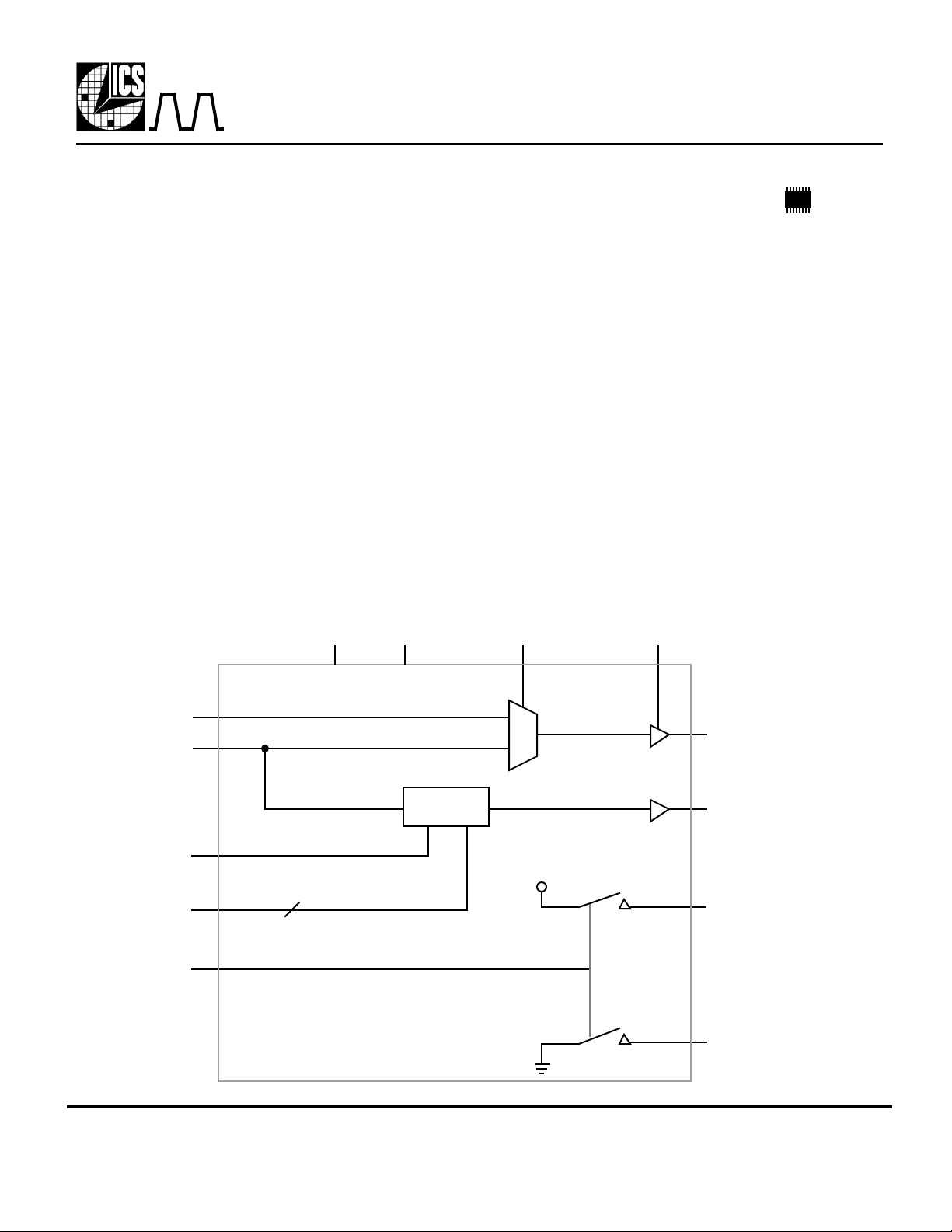
Block Diagram
INB
INA
REFIN
S2:S0
CENTER
VDD GND
3
Clock Loss
Detector
OESELB
CLKOUT
NO_INA
VDD
HIGH
LOW
GND
MDS 2042-01 1 Revision 102600 Printed 11/15/00
Integrated Circuit Systems, Inc. • 525 Race Street • San Jose • CA • 95126 • (408)295-9800tel• www.icst.com

ADVANCE INFORMATION
MK2042-01
ICRO
Pin Assignment
S0 OE
S1
S2
INB
INA
GND
SELB
Pin Descriptions
1
2
3
4
5
6
7
8
16 pin (150 mil) SOIC
16
15
14
13
12
11
10
9
C
LOCK
VDD
CLKOUT
NO_INA
HIGH
LOW
GND
CENTERREFIN
Communications Clock Monitor
Clock Loss Detector Settings
S2 S1 S0 Nominal Count
0 0 0 34
0 0 1 18
0 1 0 130
0 1 1 66
1 0 0 10
1 0 1 6
1 1 0 2
1 1 1 2
Due to the possible phase differences between
the REFIN clock and the INA clock, the
Nominal Count has a tolerance of -0/+1
REFIN clock edges.
Number Name Type Description
1 S0 I Clock Count Select 0. Determines allowed number of missing clock edges per table above.
2 S1 I Clock Count Select 1. Determines allowed number of missing clock edges per table above.
3 S2 I Clock Count Select 2. Determines allowed number of missing clock edges per table above.
4 INB I Input Clock B.
5 INA I Input Clock A.
6 GND P Connect to ground.
7 SELB I Mux select. Selects INB when high.
8 REFIN I Reference Clock Input.
9 CENTER I Enables HIGH and LOW pins when high.
10 GND P Connect to ground.
11 LOW O Sets low end of centering range.
12 HIGH O Sets high end of centering range.
13 NO_INA O Goes high when clock on INA stops.
14 CLKOUT O Clock output.
15 VDD P Connect to +3.3 V or +5 V.
16 OE I Output Enable. Tri-states CLKOUT when low.
Type: I = Input, O = output, P = power supply connection
All inputs have an internal pull-up.
MDS 2042-01 2 Revision 102600 Printed 11/15/00
Integrated Circuit Systems, Inc. • 525 Race Street • San Jose • CA • 95126 • (408)295-9800tel• www.icst.com
 Loading...