MK1714-02
Spread Spectrum Multiplier Clock
Description
The MK1714-02 is a low cost, high performance
clock synthesizer with selectable multipliers and
spread amounts (percentages), designed to
generate high frequency clocks with low EMI.
Using analog/digital Phase-Locked Loop (PLL)
techniques, the device accepts an inexpensive,
fundamental mode, parallel resonant crystal, or a
clock input to produce a spread, or dithered,
output, thereby reducing the frequency amplitude
peaks by several dB. The OE pin puts both outputs
into a high impedance state for board level testing.
The PD# pin powers down the entire chip, and the
outputs are held low.
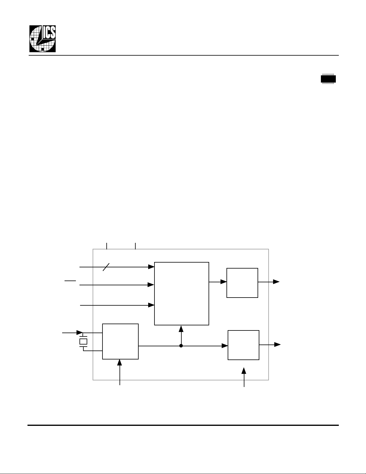
Block Diagram
VDD GND
Features
• Packaged in 20 pin tiny SSOP (QSOP)
• Operating VDD of 3.3 V or 5 V
• Multiplier modes of x1, x2, x3, x4, x5, and x6
• Inexpensive 10-25 MHz crystal, or clock input
• OE pin tri-states the outputs for testing
• Power down pin stops the outputs low
• Selectable frequency spread
• Spread can be turned on or off
• Duty cycle of 40/60
• Advanced, low power CMOS process
• Industrial temperature range available
S4:0
PD
Low EMI
Enable
Input crystal
or clock
MDS 1714-02 C 1 Revision 120400
Integrated Circuit Systems, Inc. • 525 Race Street • San Jose •CA•95126• (408) 295-9800tel • www.icst.com
X1
X2
5
Crystal
Oscillator
XSEL
PLL Clock
Multiplier and
Spread
Spectrum
Circuitry
Output
Buffer
Output
Buffer
OE (both outputs)
Clock Out
REF

Pin Assignment
MK1714-02
Spread Spectrum Multiplier Clock
X2
X1/ICLK
VDD
VDD
S4
S3
GND
GND
S2
CLK
1
2
3
4
5
6
7
8
9
10
16
15
14
13
12
11
20
19
18
17
REF
OE
PD
GND
S0
NC
S1
GND
LEE
XSEL
20 pin.150 mil SSOP (QSOP)
Pin Descriptions
Pin # Name Type Description
1 X2 XO Crystal connection. Connect to parallel mode crystal. Leave open for clock.
2 X1/ICLK XI Crystal connection. Connect to parallel mode crystal, or clock.
3 VDD P Connect to VDD. Must be same value as other VDD.
4 VDD P Connect to VDD. Must be same value as other VDD. Decouple with pin 7.
5 S4 I(D) Select pin number 4. Determines multiplier and spread amount per table on following page.
6 S3 I Select pin number 3. Determines multiplier and spread amount per table on following page.
7
8 GND P Connect to ground.
9 S2 I Select pin number 2. Determines multiplier and spread amount per table on following page.
10 CLK O Clock output which depends on the input, multiplier and spread amount per table on page 3.
11 XSEL I Connect to VDD for crystal input, or GND for CLK input.
12 LEE I Low EMI Enable. Turns on the Spread spectrum when high.
13 GND P Connect to ground.
14
15 NC - No Connect.
16 S0 I Select pin number 0. Determines multiplier and spread amount per table on following page.
17 GND P Connect to ground.
18 PD I Power Down. Turns off the chip when low. Outputs stop low.
19 OE I Output Enable. Tri-states all outputs when low.
20 REF O Reference clock output from crystal oscillator.
GND P Connect to ground.
S1 I Select pin number 1. Determines multiplier and spread amount per table on following page.
Key: I = Input with internal pull-up; I(D) = Input with internal pull-down; XO/XI = crystal connections;
O = output; P = power supply connection
MDS 1714-02 C 2 Revision 120400
Integrated Circuit Systems, Inc. • 525 Race Street • San Jose •CA•95126• (408) 295-9800tel • www.icst.com
 Loading...