MK1574
ICRO
C
LOCK
Description
The MK1574-01 is a Phase-Locked Loop (PLL)
based clock synthesizer, which accepts an 8 kHz
clock input as a reference, and generates many
popular communications frequencies. All outputs
are frequency locked together and to the input.
This allows for the generation of locked clocks to
the 8 kHz backplane clock, simplifying clock
generation and distribution in communications
systems.
MicroClock can customize this device for any
other different frequencies.
Frame Rate Communications PLL
Features
• Packaged in 16 pin narrow (150 mil) SOIC
• Exact multiplications stored in the device eliminate
the need for external dividers
• Accepts 8 kHz input clock
• Output clock rates include T1, E1, T2, E2
• 3.0V to 5.5V operation
• Available in commercial (0 to +70 C) or industrial
(-40 to +85 C) temperature ranges
• For jitter attenuation, use the MK2049
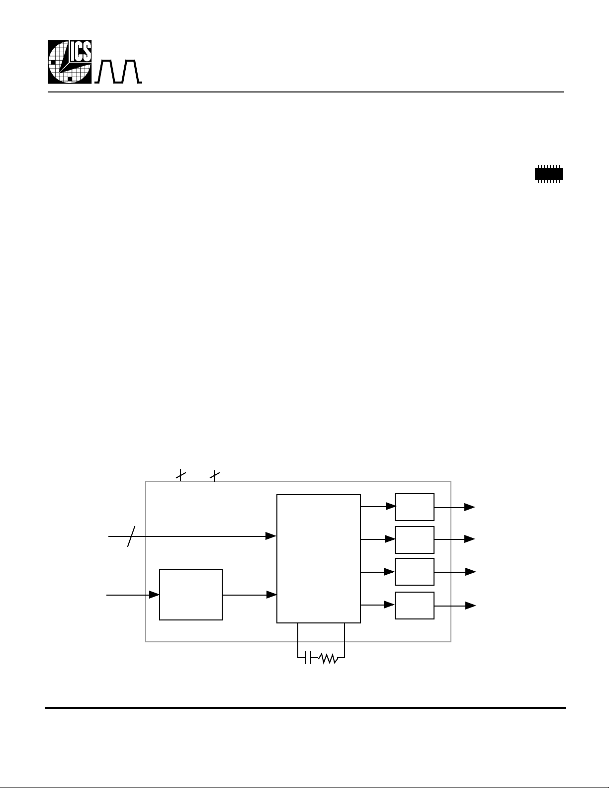
Block Diagram
VDD GND
2
4
FS0-3
8kHz
Input Clock
MDS 1574-01 D 1 Revision 011999 Printed 11/15/00
MicroClock Division of ICS • 525 Race Street • San Jose • CA • 95126•(408)295-9800tel•(408)295-9818fax
Input
Buffer
2
CAP1
PLL
Clock
Synthesis
and
Control
Circuitry
Output
Buffer
Output
Buffer
Output
Buffer
Output
Buffer
CAP2
CLK1
CLK2
CLK3
8kHz
(recovered)

MK1574
ICRO
C
LOCK
Frame Rate Communications PLL
Pin Assignment Output Clocks Decoding Table MK1574-01 (MHz)
ICLK
VDD
VDD
CAP1
GND
CAP2
GND
1
2
3
4
5
16
15
14
13
12
6
7
10
8
16 pin (150 mil) SOIC
11
9FS0
FS3
N/C
FS2
FS1
CLK3
CLK2
CLK1
8KOUT
Decode Address ICLK Multiplier CLK 1 CLK 2 CLK 3
FS3:0 (Hex) pin 1 On-chip pin 10 pin 11 pin 12
0 Reserved Reserved Reserved Reserved Reserved
0000
1 Reserved Reserved Reserved Reserved Reserved
0001
2 Reserved Reserved Reserved Reserved Reserved
0010
3 Reserved Reserved Reserved Reserved Reserved
0011
4 8.00kHz 2940 23.52 11.76 5.88
0100
5 8.00kHz 1960 15.68 7.84 3.92
0101
6 8.00kHz 2760 22.08 11.04 5.52
0110
7 8.00kHz 2640 21.12 10.56 5.28
0111
8 8.00kHz 1920 15.36 7.68 3.84
1000
9 8.00kHz 6480 51.84 25.92 12.96
1001
A 8.00kHz 2112 16.896 8.448 4.224
1010
B 8.00kHz 1578 12.624 6.312 3.156
1011
C 8.00kHz 8192 65.536 32.768 16.384
1100
D 8.00kHz 6176 49.408 24.704 12.352
1101
E 8.00kHz 1024 8.192 4.096 2.048
1110
F 8.00kHz 772 6.176 3.088 1.544
1111
• 0 = connect directly to ground, 1 = connect directly to VDD.
Pin Descriptions
Number Name Type Description
1 ICLK I Input clock. Connect to an 8kHz clock input.
2 VDD P Connect to +3.3V or +5V.
3 VDD P Connect to +3.3V or +5V. Must be same voltage as pin 2.
4 CAP1 I Connect a ceramic capacitor and a resistor in series between this pin and CAP2. Refer to page 4.
5 GND P Connect to ground.
6 CAP2 I Connect a ceramic capacitor and a resistor in series between this pin and CAP1. Refer to page 4.
7 GND P Connect to ground.
8 FS0 I Frequency Select 0. Determines CLK outputs per table above.
9 8KOUT O Recovered 8kHz output clock. Can be lower jitter, better duty cycle than input clock.
10 CLK1 O Clock 1 determined by status of FS3:0 per table above.
11 CLK2 O Clock 2 determined by status of FS3:0 per table above.
12 CLK3 O Clock 3 determined by status of FS3:0 per table above.
13 FS1 I Frequency Select 1. Determines CLK outputs per table above.
14 FS2 I Frequency Select 2. Determines CLK outputs per table above.
15 N/C - No Connect. Nothing is connected to this pin.
16 FS3 I Frequency Select 3. Determines CLK outputs per table above.
Type: I = Input, O = output, P = power supply connection
MDS 1574-01 D 2 Revision 011999 Printed 11/15/00
MicroClock Division of ICS • 525 Race Street • San Jose • CA • 95126•(408)295-9800tel•(408)295-9818fax
 Loading...