MK1573-02
GenClock ™ HSYNC to Video Clock
Description
The MK1573 GenClock™ provides genlock
timing for video overlay systems. The device
accepts the horizontal sync (HSYNC) signal as the
input reference clock, and generates a frequencylocked high speed output. Stored in the device are
the multipliers for 16 combinations of popular
frequencies for analog and digital TV and set-top
box systems. Frequency-locked outputs include
1X, 4X, and 8X the subcarrier frequencies of
NTSC and PAL systems, and 27MHz plus
13.5MHz for digital video systems. In most
selections, the chip recovers the HSYNC clock by
outputting a low jitter 50% duty cycle version of
HSYNC. Also available is an inverted recovered
HSYNC clock, and a double speed recovered
HSYNC clock.
MicroClock can customize this device for any
other different frequencies.
Features
• Packaged in 16 pin narrow (150 mil) SOIC
• The -02 version has one frequency changed
(32MHz was added), and tracks the HSYNC
better than the -01 version.
• Exact ratios stored in the device eliminate the need
for external dividers
• Accepts HSYNC of 15.625kHz or 15.73426kHz
• Highly accurate frequency generation within 1 ppm
• Generates NTSC/PAL subcarrier frequencies, and
4X and 8X of those frequencies
• Generates 27MHz and 13.5MHz
• 2X HSYNC clock available
• Recovered HSYNC clock available
• Inverted HSYNC clock available
• 4.5V to 5.5V operation
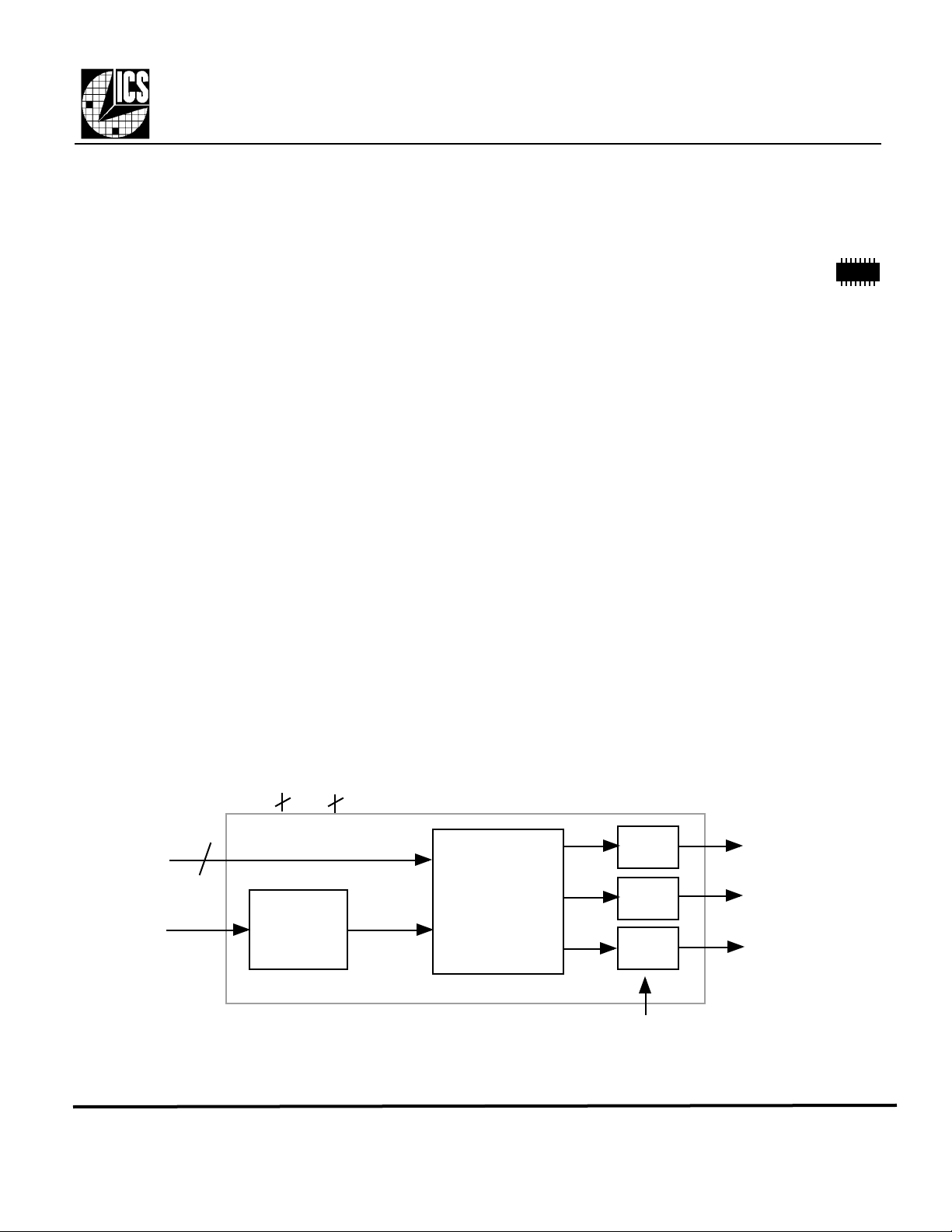
Block Diagram
VDD GND
2
FS0-3
HSYNC
Input Clock
MDS 1573-02 B 1 Revision 120497 Printed 11/15/00
Integrated Circuit Systems, Inc. • 525 Race Street • San Jose • CA • 95126•(408)295-9800tel•www.icst.com
4
Input
Buffer
2
Clock
Synthesis
and
Control
Circuitry
Output
Buffer
Output
Buffer
Output
Buffer
OE (all outputs)
CLK1
CLK2
CLK3

MK1573-02
GenClock ™ HSYNC to Video Clock
Pin Assignment Output Clocks Decoding Table MK1573-02 (MHz)
HSYNC
VDD
VDD
CAP1
GND
CAP2
GND
16 pin (150 mil) SOIC
1
2
3
4
5
6
7
8
16
15
14
13
12
11
10
FS3
N/C
FS2
FS1
CLK2
OE
CLK1
9FS0
CLK3
Decode Address HSYNC Multiplier CLK 1 CLK 2 CLK 3
FS3:0 (Hex) pin 1 On-chip pin 10 pin 12 pin 9
0 15.625k 1536 24M 12M 15.625k
0000
1 15.734264k 1525 1/3 24M 12M 15.734264k
0001
2 15.625k 1728 27M 13.5M 15.625k
0010
3 15.734264k 1716 27M 13.5M 15.734264k
0011
4 15.625k 960 15M 7.5M 15.625k
0100
5 15.734264k 953 1/3 15M 7.5M 15.734264k
0101
6 15.625k 3840 60M 30M 15.625k
0110
7 15.734264k 3840 60.41957M 30.20979M 15.734264k
0111
8 15.625k 2270 35.46875M 17.734375M 4.433594M
1000
9 15.734264k 1820 28.63636M 14.31818M 3.579545M
1001
A 15.625k 2270 35.46875M 15.625k 15.625k
1010
B 15.734264k 1820 28.63636M 15.734264k 15.734264k
1011
C 15.625k 2048 32M 16M 15.625k
1100
D 15.734264k 808 12.71329M 15.734264k 31.4685k
1101
E 15.625k 2270 35.46875M 15.625k 31.25k
1110
F 15.734264k 1820 28.63636M 15.734264k 31.4685k
1111
• 0 = connect directly to ground, 1 = connect directly to VDD.
• CLK2 is a recovered HSYNC (with 50% duty cycle) on selections in italic.
• HSYNC reference outputs on CLK3 (in italic) are inverted, recovered HSYNC.
Pin Descriptions
Number Name Type Description
1 HSYNC I HSYNC clock input. The output clocks are synchronized to the HSYNC falling edge.
2 VDD P Connect to +5V.
3 VDD P Connect to +5V.
4 CAP1 I Connect a 0.01µF ceramic capacitor and a 39kΩ resistor in series between this pin and CAP2.
5 GND P Connect to ground.
6 CAP2 I Connect a 0.01µF ceramic capacitor and a 39kΩ resistor in series between this pin and CAP1.
7 GND P Connect to ground.
8 FS0 I Frequency Select 0. Determines CLK outputs (with given input) per table above.
9 CLK3 O Clock 3 determined by status of FS3:0 per table above.
10 CLK1 O Clock 1 determined by status of FS3:0 per table above.
11 OE I Output Enable. Tri-states the three output clocks when low.
12 CLK2 O Clock 2 determined by status of FS3:0 per table above.
13 FS1 I Frequency Select 1. Determines CLK outputs (with given input) per table above.
14 FS2 I Frequency Select 2. Determines CLK outputs (with given input) per table above.
15 N/C - No Connect. Nothing is connected to this pin.
16 FS3 I Frequency Select 3. Determines CLK outputs (with given input) per table above.
Type: I = Input, O = output, P = power supply connection
MDS 1573-02 B 2 Revision 120497 Printed 11/15/00
Integrated Circuit Systems, Inc. • 525 Race Street • San Jose • CA • 95126•(408)295-9800tel•www.icst.com
 Loading...