ICST MK1491-06S, MK1491-06STR, MK1491-06R, MK1491-06RTR Datasheet

MK1491-06
CS5530 Geode™ Clock Source
Description
The MK1491-06 is a low cost, low jitter, high
performance clock synthesizer for National
Semiconductor CS5530 based computer and
portable appliance applications. Using patented
analog Phase-Locked Loop (PLL) techniques,
the device accepts a 14.318 MHz crystal input to
produce multiple output clocks. It provides
selectable PCI local bus and AC97 audio clocks,
24 MHz and 48 MHz clocks for Super I/O and
USB, as well as multiple Reference outputs.
The device has multiple power down modes to
reduce power consumption.
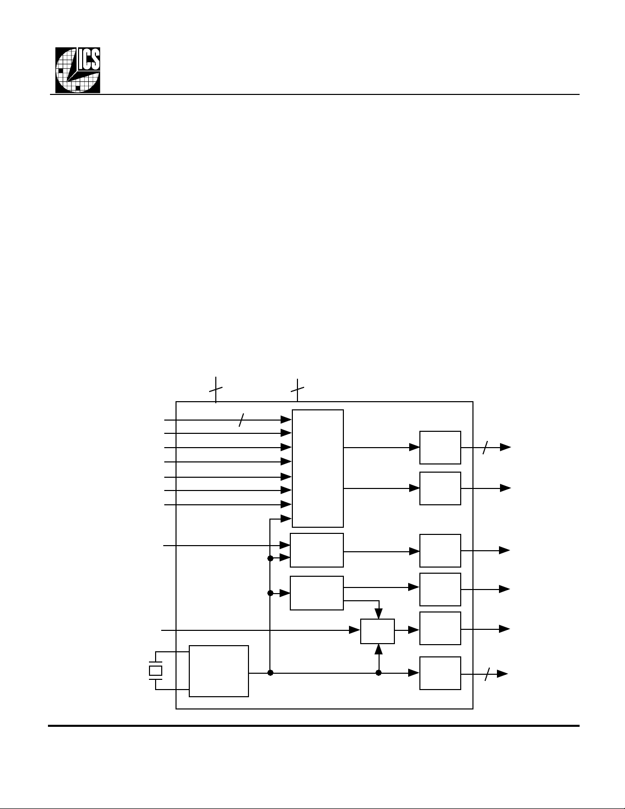
Block Diagram
PCI Frequency Select
Low EMI Enable
PCIF Function Enable
Early PCI Enable
SLOW#
PCISTP#
PWRDWN#
VDD GND
2
Features
• Packaged in 28 pin, 300 mil wide SOIC or in
28 pin, 150 mil wide SSOP
• Provides all critical timing for the National
Semiconductor CS5530 Geode companion chip
• Four PCI clocks
• Selectable PCIF on up to 2 outputs
• Early PCI clock selectability
• Up to 4 Reference clocks
• 48 MHz USB and 24MHz SIO support
• AC97 audio clock
• Multiple power down modes
• Low EMI Enable pin reduces EMI radiation on
PCI clocks (patented)
• 3.3 V ±5% operation
56
3
PCI
EPCI/PCI
PCI
Clocks
Output
Buffers
Output
Buffer
Audio Select
14.3M/24M Select
XI
14.31818 MHz
crystal
XO
MDS 1491-06 F 1 Revision 101700 Printed 11/15/00
Crystal
Oscillator
Audio
Clock
Fixed
Clocks
MUX
Output
Buffer
Output
Buffer
Output
Buffer
Output
Buffers
3
16.934 MHz or
24.576 MHz or
49.152 MHz
48 MHz
14.318 MHz or
24 MHz
14.318 MHz
Integrated Circuit Systems, Inc. • 525 Race Street • San Jose • CA • 95126 • (408)295-9800tel • www.icst.com

MK1491-06
CS5530 Geode™ Clock Source
Pin Assignment
VDD
XI
XO
GND
14.3M(TS)
14.3M
GND
14.3M(SEL AUDIO)
VDD
SLOW#
GND
FS
SEL24
VDD
1
2
3
4
5
6
7
8
9
10
11
12
13
14
AC97 AUDIO(PEN)
28
PCI
27
VDD
26
PCI
25
PCI
24
23
GND
22
PCI(EPCI#)
21
48M(LE#)
20
VDD
19
24M/14.3M
18
VDD
17
GND
16
PCISTP#
15
PWRDWN#
24M/14.3M Frequency
Select Table
SEL24 24M/14.3M
0 14.31818 MHz
1 24.0 MHz
PCIF Enable Control
PEN Pin 25 Pin 24
0 PCI PCI
M PCI PCIF
1 PCIF PCIF
PCIF continues to run in PCI STOP
mode. See table on page 4.
PCI Frequency Select Table
TS FS PCI
0 0 Tristate all clocks
0 1 Reserved
M 0 30 MHz
M 1 33.3 MHz
1 0 25 MHz
1 1 37.5 MHz
Early PCI Control Table
EPCI# PCI (Pin 22)
0
1
1 ns early
Normal
EMI Control
AC97 Audio Frequency Select
SEL AUDIO AC97 AUDIO
0 16.9344 MHz
M 24.576 MHz
1 49.152 MHz
LE# PCI Low EMI
0 ON
1 OFF
Spread direction is DOWN..
Pin Descriptions
Pin # Name Type Description
1, 9, 14 VDD P Connect to +3.3V. Must be same voltage on all pins.
2 XI I Crystal connection. Connect to a 14.31818 MHz crystal or input clock.
3 XO O Crystal connection. Connect to a 14.31818 MHz crystal, or leave unconnected for clock.
4, 7, 11, 17, 23 GND P Connect to Ground.
5 14.3M(TS) TI/O 14.318 MHz output. Input control for all clocks per table above.
6 14.3M O 14.318 MHz buffered reference clock output.
8 14.3M(SEL AUDIO) TI/O 14.318 MHz output and audio frequency select input per table above.
10 SLOW# I PCI normal or slow mode select input per table on page 4.
12 FS I Frequency Select for PCI clocks per table above.
13 SEL24 I Fixed frequency select input per table above. Selects frequency on pin 19.
15 PWRDWN# I Power down control; defined in table on page 4.
16 PCISTP# I PCI Stop power down control; defined in table on page 4.
18, 20, 26 VDD P Connect to +3.3V. Must be same voltage on all pins.
19 24M/14.3M O Fixed frequency clock output per table above.
21 48(LE#) I/O Fixed frequency clock output and low EMI (spread spectrum) enable input per table above.
22 PCI(EPCI#) I/O PCI Output clock that can be early. Input control for Early PCI per table above.
24 PCI O PCI Output clock. PCI/PCIF control set by PEN per table above.
25 PCI O PCI Output clock. PCI/PCIF control set by PEN per table above.
27 PCI O PCI Output clock.
28 AC97 AUDIO(PEN) TI/O Audio clock output and PCIF Function Enable per table above.
Key: I = Input, TI = tri-level input, O = Output, P = Power supply connection, (T)I/O = Input on power up, becomes an Output after 10ms.
Weak internal pull-up resistors are present on SEL24, EPCI#, FS, LE#, PCISTP#, and SLOW#. These pins should be tied to VDD or GND,
and not be left floating. Internal resistors on PEN, SEL AUDIO, and TS pull to a mid-level (M).
MDS 1491-06 F 2 Revision 101700 Printed 11/15/00
Integrated Circuit Systems, Inc. • 525 Race Street • San Jose • CA • 95126 • (408)295-9800tel • www.icst.com
 Loading...