MK1449B
Sound/SCSI+Fast Ethernet Clock
Description
The MK1449B is the most cost effective way to
generate high quality, high frequency clock
outputs for SCSI plus Fast Ethernet devices, or
AC97 sound chips. Using Phase-Locked-Loop
(PLL) techniques, the device uses a standard
fundamental mode, inexpensive 14.31818 MHz
crystal or clock to produce two output clocks.
The device can accept either a crystal or clock
input. Also on the chip is the ability to generate a
1.25x clock of the reference plus the reference,
making it possible to generate 20 and 25 MHz
clocks from a 20 MHz crystal.
Features
• Packaged as 8 pin SOIC
• For Fast Ethernet plus SCSI on computer
motherboards
• For AC97 sound on computer motherboards
• Less than 1 ppm synthesis error
• Input crystal frequency of 14.31818 MHz
• Operating voltages of 3.0 to 5.5V
• Available in industrial temperature
• Full CMOS level outputs with 25mA drive
capability at TTL levels
• Ideal for oscillator replacement
• Advanced, low power CMOS process
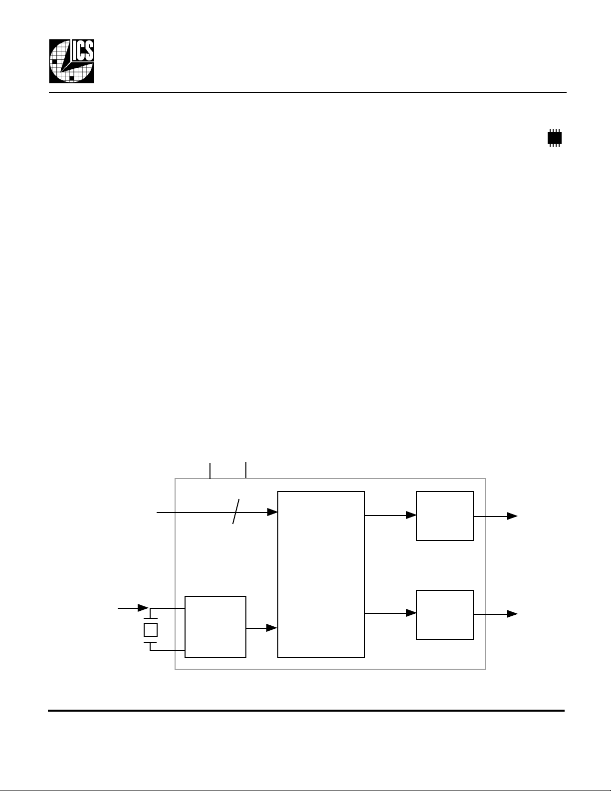
Block Diagram
S1, S0
14.31818MHz
crystal
or clock
X1
X2
VDD GND
2
Crystal
Oscillator
PLL
Clock
Synthesis
and Control
Circuitry
Output
Buffer
Output
Buffer
CLK1
CLK2
MDS 1449B C 1 Revision 120799 Printed 11/15/00
Integrated Circuit Systems, Inc. • 525 Race Street • San Jose •CA•95126• (408)295-9800tel • www.icst.com

MK1449B
Sound/SCSI+Fast Ethernet Clock
Pin Assignment
X1/ICLK
VDD
GND
CLK2
1 8
2
3
4
X2
7
S1
6
S0
5
CLK1
Clock Decoding Table (MHz)
S1 S0 CLK1 CLK2
0 0 test test
0 1 40 25
1 0 49.152 12.288
1 1 x1.25 Reference
0 = connect directly to ground.
1 = connect directly to VDD.
In the 1,1 mode, crystals or clocks from
5 to 27 MHz can be used as an input.
Pin Descriptions
Number Name Type Description
1 X1/ICLK I Crystal connection or clock input. Connect to a 14.31818MHz parallel resonant crystal.
2 VDD P Connect to +3.3V or +5V.
3 GND P Connect to ground.
4 CLK2 O Clock 2 output per Table above.
5 CLK1 O Clock 1 output per Table above.
6 S0 I Select 0 for output clocks. Connect to GND or VDD. See table above.
7 S1 I Select 1 for output clocks. Connect to GND or VDD. See table above.
8 X2 O Crystal connection to a 14.31818 MHz crystal. Leave unconnected for clock input.
Key: I = Input, O = output, P = power supply connection
MDS 1449B C 2 Revision 120799 Printed 11/15/00
Integrated Circuit Systems, Inc. • 525 Race Street • San Jose •CA•95126• (408)295-9800tel • www.icst.com
 Loading...