

MK1442/MK1443
SCSI and Ethernet Clock Source
Description
The MK1442/3 are the ideal way to generate
clocks for desktop computer motherboards and
LAN workstations. Using analog Phase-Locked
Loop (PLL) techniques, the devices accept a
14.318 MHz crystal input to produce multiple
output clocks up to 100 MHz. They provide
2XCPU, CPU, floppy controller, keyboard,
system, SCSI and Ethernet clocks. The MK1442/3
are perfect for new Pentium™ Processor, PCI bus
and 486 systems. The devices can operate at 5V or
3.3V up to and including 80MHz on the CPU
clock.
The devices are identical except the MK1442 has
an Output Enable (OE) pin that tri-states all
outputs when taken low, and the MK1443 has an
extra 14.318 MHz clock.
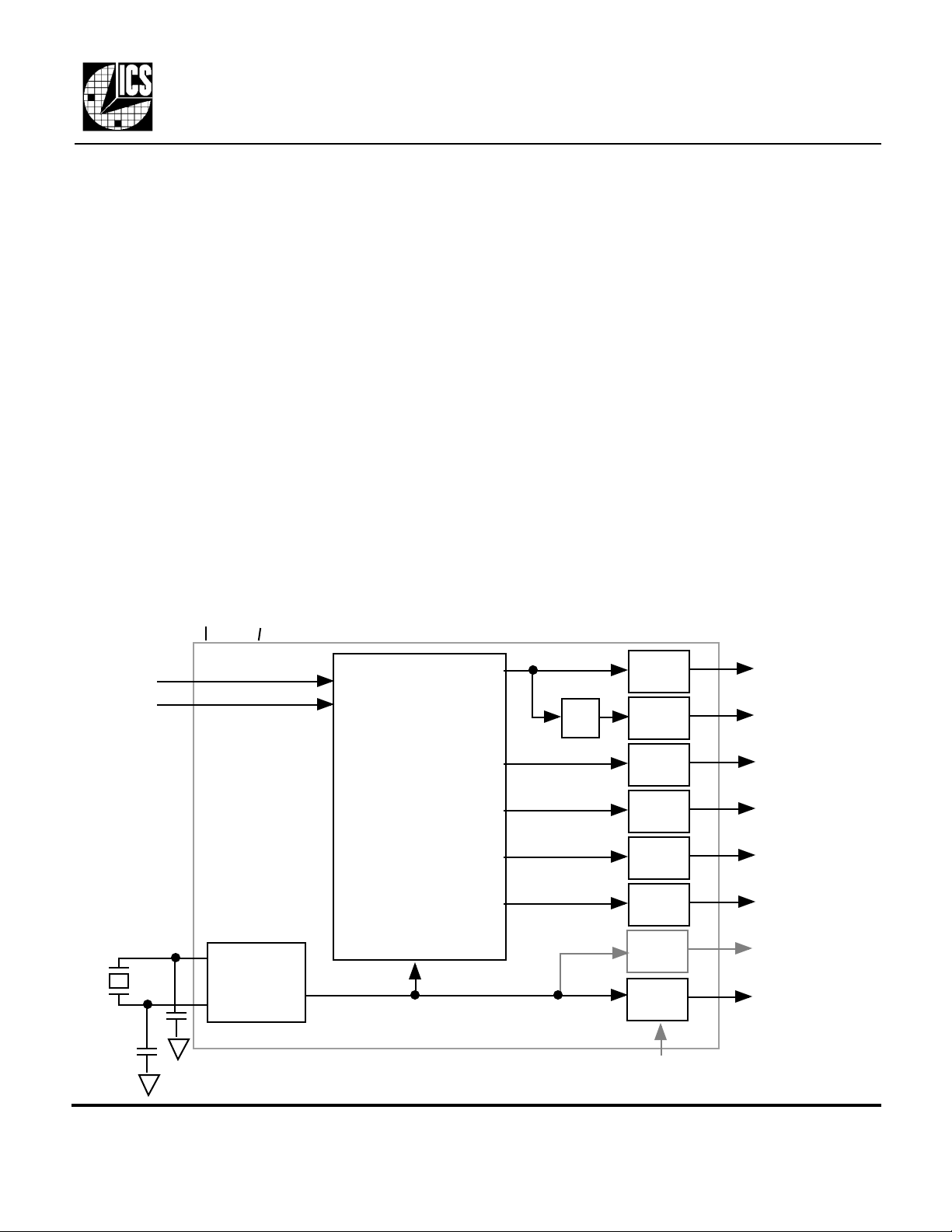
Block Diagram
VDD
GND
Features
• Provides exact frequency Ethernet and SCSI clocks
• 5V or 3.3V (up to 80MHz) operation
• Output clock frequencies up to 100 MHz
• Pentium™ Processor compatible timing
• 486 compatible smooth frequency transitions
• Seven or eight output clocks
• Compatible with X86 and 680X0 CPUs
• Skew controlled 2X and 1X CPU to within 250ps
• Packaged in 16 pin skinny SOIC or PDIP
• Duty cycle of 47.5/52.5 up to 66.66 MHz
• Duty cycle of 45/55 up to 100 MHz
• Total of 15 different selectable CPU frequencies
• Tri-state outputs for board level testing
• 25mA drive capability at TTL levels
• Keyboard frequencies of 12MHz (-01),
8MHz (-02), or 16MHz (-03)
• Advanced, low power CMOS process
• MK1442 - output enable
• MK1443 - two 14.318 MHz outputs
CPUS0
CPUS1
14.318 MHz
crystal
X1
X2
Crystal
Oscillator
Clock Synthesis
and Control
Circuitry
÷2
Output
Buffer
Output
Buffer
Output
Buffer
Output
Buffer
Output
Buffer
Output
Buffer
Output
Buffer
2XCPU
CPU
8.00, 12.00,
or 16.00 MHz
24.00 MHz
40.000 MHz
20.000 MHz
14.318 MHz
(MK1443 only)
Output
Buffer
14.318 MHz
OE (all outputs, MK1442 only)
MDS 1442/3 E 1 Revision 111500 Printed 11/15/00
Integrated Circuit Systems, Inc. • 525 Race Street • San Jose • CA • 95126 •(408)297-1201tel • www.icst.com
MK1442/MK1443
SCSI and Ethernet Clock Source
Pin Assignment
CPUS1
X2
X1
VDD
GND
24M
40M
20M
1
2
3
4
5
6
7 10
8 9
16
15
14
13
12
11
CPUS0
2XCPU
CPU
VDD
GND
14.3M
OE or 14.3M
(MK1442) (MK1443)
KBOUT
Pin Descriptions
Number Name Type Description
1 CPUS1 TI Select 1 for 2XCPU and CPU frequencies. See Table above, note 5 below.
2 X2 O Crystal connection. Connect to 14.318 MHz crystal, or leave unconnected for clock input.
3 X1 I Crystal connection. Connect to 14.318 MHz crystal, or drive with a 14.318MHz clock.
4 VDD P Connect to +5V or 3.3V. Must be same voltage as pin 13.
5 GND P Connect to ground.
6 24M O 24.00 MHz floppy (or super I/O) clock output.
7 40M O 40.00 MHz clock output
8 20M O 20.000 MHz Ethernet clock output
9 KBOUT O Keyboard clock. 12.00 MHz on -01, 8.00 MHz on -02, 16.00 MHz on -03 version.
10 OE I Output Enable on 1442. Tri-states all clock outputs when this input is low. Internal pull-up.
11 14.3M O 14.318 MHz system clock output.
12 GND P Connect to ground.
13 VDD P Connect to +5V or 3.3V. Must be same voltage as pin 4.
14 CPU O CPU output. See Table above. Rising edge is within 250ps of 2XCPU.
15 2XCPU O 2XCPU output. See Table above. Rising edge is within 250ps of CPU.
16 CPUS0 TI Select 0 for 2XCPU and CPU frequencies. See Table above, note 5 below.
CPU Clock Decoding
CPUS1 CPUS0 2XCPU (MHz) CPU (MHz)
0 0 8.00 4.00
0 M 80.00 40.00
0 1 33.33 16.67
M 0 100.00 (note 4) 50.00 (note 4)
M M 66.67 33.33
M 1 60.00 30.00
1 0 50.00 25.00
1 M 20.00 10.00
1 1 25.00 12.50
Notes:
1. M = mid point (input is left floating. See note 5 below)
2. Actual frequencies are within 0.05% of those shown.
3. Transitions between mean frequencies are smooth, and do not
violate Intel’s 0.1% per cycle specification.
4. These selections are not guaranteed to operate at 3V
Key: I = Input, TI = three level input, O = output, P = power supply connection
Note 5: The TI inputs are internally held at mid-level, so they cannot drift high or low.
Crystal and Capacitor Selection for Ethernet Accuracy
The MK1442/3 requires external crystals between the X1 and X2 pins and ground, as shown on the block
diagram on page 1. For an accurate Ethernet frequency of 20.000 MHz, a 14.31818 MHz ±50 ppm,
parallel resonant crystal with a load capacitance of 16pF is recommended, along with 22 pF ±5% (NPO
dielectric) chip capacitors. If the 20 MHz output is not used for Ethernet, any 22 pF capacitors will work.
MDS 1442/3 E 2 Revision 111500 Printed 11/15/00
Integrated Circuit Systems, Inc. • 525 Race Street • San Jose • CA • 95126 •(408)297-1201tel • www.icst.com

MK1442/MK1443
ABSOLUTE MAXIMUM RATINGS (note 1)
DC CHARACTERISTICS (VDD = 5V unless noted)
Leave pin unconnected or tri-stated
AC CHARACTERISTICS (VDD = 5V unless noted)
exposure to levels above the operating limits but below the Absolute Maximums may affect device reliability.
2. Provided proper crystal and capacitor components are used - consult MicroClock.
SCSI and Ethernet Clock Source
Electrical Specifications
Parameter Conditions Minimum Typical Maximum Units
Supply voltage, VDD Referenced to GND 7 V
Inputs and Clock Outputs Referenced to GND -0.5 VDD+0.5 V
Ambient Operating Temperature 0 70 °C
Soldering Temperature Max of 20 seconds 260 °C
Storage Temperature -65 150 °C
Operating Voltage, VDD 3.0 5.5 V
Input High Voltage, VIH OE (pin 10) 2.0 V
Input Low Voltage, VIL OE (pin 10) 0.8 V
Input High Voltage, VIH CPUS0,1 (pins 1,16) VDD-0.5 V
Input Mid-level Voltage CPUS0,1 (pins 1,16)
Input Low Voltage, VIL CPUS0,1 (pins 1,16) 0.5 V
Output High Voltage, VOH IOH=-4mA VDD-0.4 V
Output High Voltage, VOH IOH=-25mA 2.4 V
Output Low Voltage, VOL IOL=25mA 0.4 V
Input High Voltage, VIH VDD=3.3V, OE pin 1.9 V
Input Low Voltage, VIL VDD=3.3V, OE pin 0.4 V
Output High Voltage, VOH VDD=3.3V, IOH=-8mA 2.4 V
Output Low Voltage, VOL VDD=3.3V, IOL=8mA 0.4 V
Operating Supply Current, IDD No Load, 80 MHz 35 mA
Short Circuit Current Each output ±100 mA
On-Chip Pull-up Resistor 250 kΩ
Input Capacitance 7 pF
Frequency Accuracy of 20.000 MHz clock 0-70°C, note 2 -1 1 ppm
V
Input Frequency 14.31818 MHz
Output Clock Rise Time 0.8 to 2.0V 1.5 ns
Output Clock Fall Time 2.0 to 0.8V 1.5 ns
Output Clock Duty Cycle, CPU and 2XCPU 1.5V, up to 67MHz 47.5 49 to 51 52.5 %
Output Clock Duty Cycle At 1.5V 45 49 to 51 55 %
Cycle to Cycle Jitter 50-80 MHz clocks 250 ps
Skew of 2XCPU with respect to CPU Rising edges at 1.5V -250 0 250 ps
Transition time, 8MHz to 100MHz VDD=3.3 or 5V 4 ms
Transition time, 100MHz to 8MHz VDD=3.3 or 5V 2.5 ms
Output Enable Time, OE high to output on VDD=3.3 or 5V 50 ns
Output Disable Time, OE low to tri-state VDD=3.3 or 5V 3 µs
Notes: 1. Stresses beyond those listed under Absolute Maximum Ratings could cause permanent damage to the device. Prolonged
MDS 1442/3 E 3 Revision 111500 Printed 11/15/00
Integrated Circuit Systems, Inc. • 525 Race Street • San Jose • CA • 95126 •(408)297-1201tel • www.icst.com

MK1442/MK1443
Inches
Millimeters
SCSI and Ethernet Clock Source
Package Outline and Package Dimensions
E H
h x 45°
D
Q
e
b
c
16 pin SOIC narrow
Symbol Min Max Min Max
A 0.055 0.070 1.397 1.778
b 0.013 0.019 0.330 0.483
c 0.007 0.010 0.191 0.254
D 0.385 0.400 9.779 10.160
E 0.150 0.160 3.810 4.064
H 0.225 0.245 5.715 6.223
e
h 0.016 0.406
Q 0.004 0.01 0.102 0.254
A
Ordering Information
Part/Order Number Marking Keyboard frequency Package Temperature
MK1442-01S MK1442-01S 12 MHz 16 pin SOIC 0-70°C
MK1442-02S MK1442-02S 8 MHz 16 pin SOIC 0-70°C
MK1442-03S MK1442-03S 16 MHz 16 pin SOIC 0-70°C
MK1443-01S MK1443-01S 12 MHz 16 pin SOIC 0-70°C
MK1443-02S MK1443-02S 8 MHz 16 pin SOIC 0-70°C
MK1443-03S MK1443-03S 16 MHz 16 pin SOIC 0-70°C
MK144x-0xSTR MK144x-0xS x Add Tape & Reel 0-70°C
While the information presented herein has been checked for both accuracy and reliability, MicroClock Incorporated assumes no responsibility for either its use or for the
infringement of any patents or other rights of third parties, which would result from its use. No other circuits, patents, or licenses are implied. This product is intended for use in
normal commercial applications. Any other applications such as those requiring extended temperature range, high reliability, or other extraordinary environmental requirements
are not recommended without additional processing by MicroClock. MicroClock reserves the right to change any circuitry or specifications without notice. MicroClock does not
authorize or warrant any MicroClock product for use in life support devices or critical medical instruments.
Pentium™ is a registered trademark of Intel Corporation
MDS 1442/3 E 4 Revision 111500 Printed 11/15/00
Integrated Circuit Systems, Inc. • 525 Race Street • San Jose • CA • 95126 •(408)297-1201tel • www.icst.com
 Loading...