

MK1412
MPEG Audio Clock Synthesizer
Description
The MK1412 is the ideal way to generate clocks
for MPEG audio devices in computers. The device
uses ICS/MicroClock’s proprietary mixture of
analog and digital Phase-Locked Loop (PLL)
technology to synthesize one of eight frequencies
(four on each output) from the 14.31818 MHz
reference. In an 8 pin SOIC, the MK1412 can save
component count, board space, and cost over
crystals and oscillators, and increase reliability by
eliminating three expensive mechanical devices
from the board.
We offer many other clocks for computers and
computer peripherals. Consult us when you need
to remove crystals and oscillators from your board.
Due to a long lead time in the original wafer fab
that makes the MK1412S, we have retooled the
die and now call the part the MK1412A. All
functional parameters are the same as or better
than the original part.
Features
• Packaged in 8 pin SOIC
• Input crystal or clock frequency of 14.31818 MHz
• Provides master MPEG clocks for 32 kHz,
44.1 kHz, 48 kHz and 96 kHz sampling rates
• Output clock frequencies of 256x and 512x of the
audio sampling rates compatible with most DACs
• Low jitter
• Full CMOS output swing with 25mA drive
capability at TTL levels
• 3.3V or 5V±10% supply voltage
• Advanced, low power CMOS process
• The A version is the newest version in a more
advanced manufacturing process
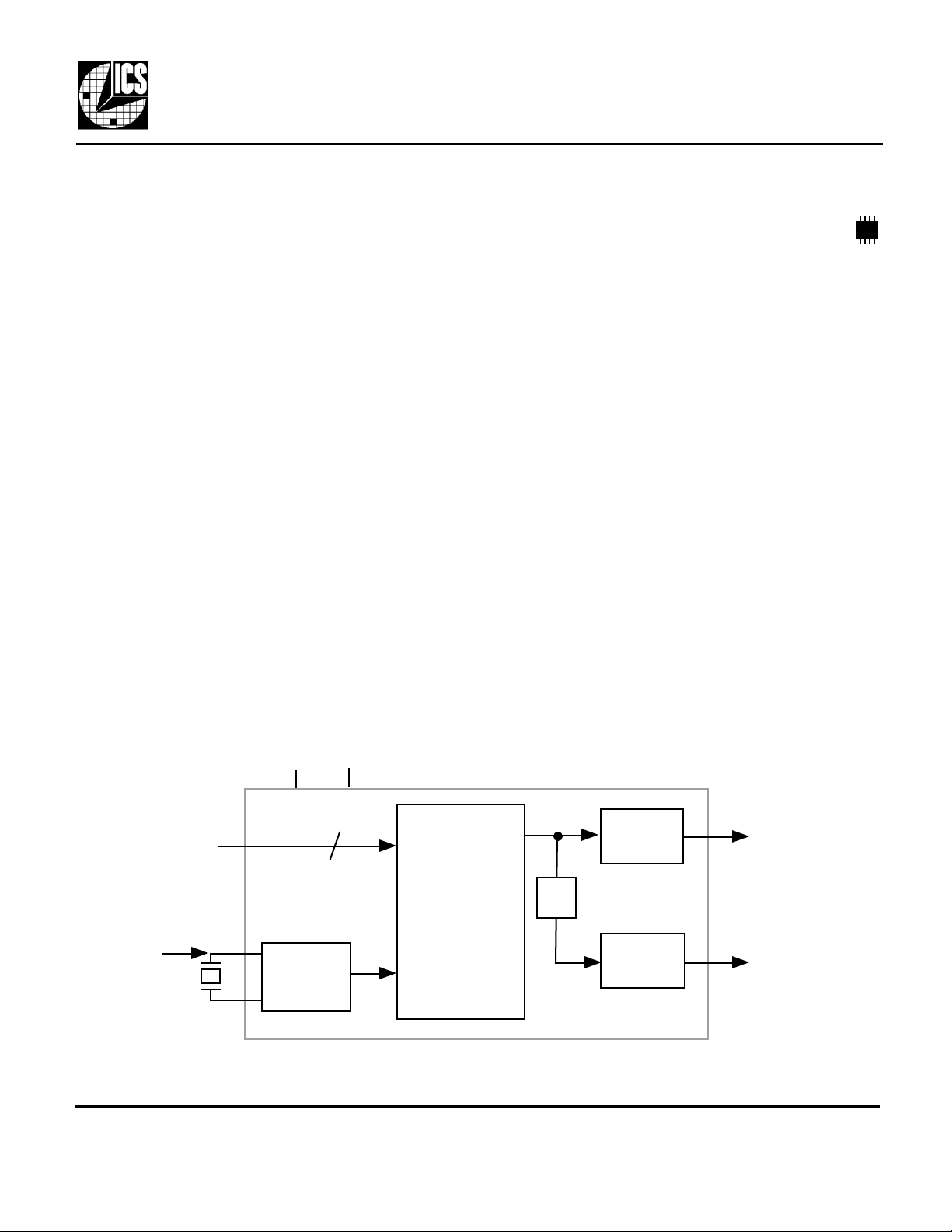
Block Diagram
VDD GND
2
S1, S0
PLL
14.31818 MHz
crystal or clock
X1
Crystal
Oscillator
X2
MDS 1412 B 1 Revision 060200 Printed 11/15/00
Integrated Circuit Systems, Inc.• 525 Race Street• San Jose • CA • 95126• (408)295-9800tel •www.icst.com
Clock Synthesis
and Control
Circuitry
÷ 2
Output
Buffer
Output
Buffer
CLK
CLK/2
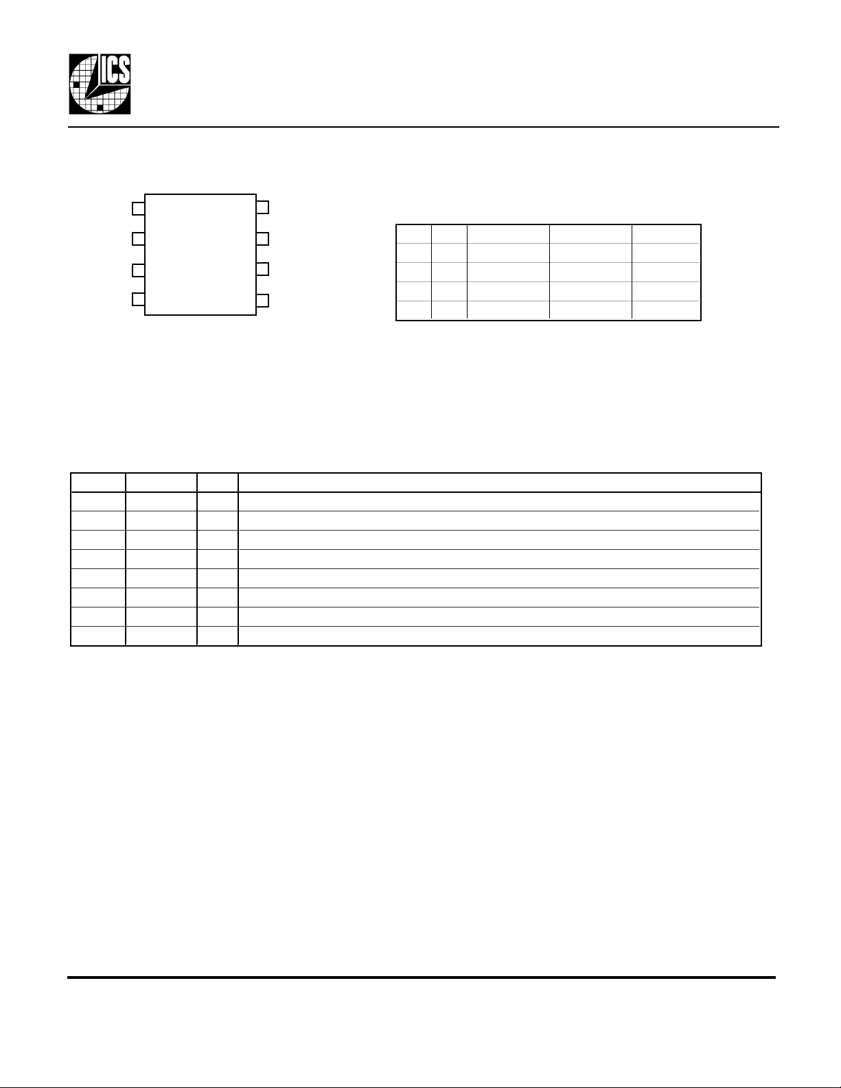
Pin Assignment
MK1412
MPEG Audio Clock Synthesizer
X1
VDD CLK
GND
CLK/2
1 8
2
3
4
7
6
5
X2
S1
S0
Audio Clock Outputs Select Table (MHz)
S1 S0 CLK CLK/2 Accuracy
0 0 16.384 8.192 1 ppm
0 1 22.5792 11.2896 25 ppm
1 0 24.576 12.288 1 ppm
1 1 49.152 24.576 1 ppm
8 pin SOIC
Pin Descriptions
Number Name Type Description
1 X1 I Crystal Connection. Connect to a 14.31818 MHz crystal or clock.
2 VDD P Connect to +3.3V or +5V.
3 GND P Connect to ground.
4 CLK/2 O Audio Clock divide by 2 output as per table above.
5 S0 I Frequency Select 0 Input. Determines CLK and CLK/2 outputs as per table above.
6 S1 I Frequency Select 0 Input. Determines CLK and CLK/2 outputs as per table above.
7 CLK O Audio Clock output as per table above.
8 X2 O Crystal Connection to a 14.31818 MHz crystal, or leave unconnected for clock input.
Key: I = Input, O = output, P = power supply connection
External Components/Crystal Selection
A minimum number of external components are required for proper oscillation. For a crystal input, one
load capacitor can be connected to each of the X1 and X2 pins and ground, and a parallel resonant
14.31818 MHz crystal is recommended. The value (in pF) of each crystal load capacitor should equal
(CL-18)*2, where CL is the crystal’s load (correlation) capacitance in pF. So for crystals with 18 pF load
capacitance (or less), no extra capacitors are needed. The frequency tolerance of the crystal should be
50ppm or better. For a clock input, connect to X1 and leave X2 unconnected. A decoupling capacitor of
0.1µF should be connected between VDD and GND on pins 2 and 3, and 33Ω terminating resistor may
be used on the clock outputs if the trace is longer than 1 inch.
MDS 1412 B 2 Revision 060200 Printed 11/15/00
Integrated Circuit Systems, Inc.• 525 Race Street• San Jose • CA • 95126• (408)295-9800tel •www.icst.com

MK1412
ABSOLUTE MAXIMUM RATINGS (note 1)
DC CHARACTERISTICS (at 5.0V unless otherwise noted)
AC CHARACTERISTICS (at 5.0V unless otherwise noted)
MPEG Audio Clock Synthesizer
Electrical Specifications
Parameter Conditions Minimum Typical Maximum Units
Supply Voltage, VDD Referenced to GND 7 V
Inputs Referenced to GND -0.5 VDD+.5V V
Clock Outputs Referenced to GND -0.5 VDD+.5V V
Ambient Operating Temperature 0 70 °C
Soldering Temperature Max of 10 seconds 260 °C
Storage temperature -65 150 °C
Operating Voltage, VDD 3 5.5 V
Input High Voltage, VIH, input clock only Clock input (VDD/2)+1 VDD/2 V
Input Low Voltage, VIL, input clock only Clock input VDD/2 (VDD/2)-1 V
Output High Voltage, VOH IOH=-4mA VDD-0.4 V
Output High Voltage, VOH IOH=-25mA 2.4 V
Output Low Voltage, VOL IOL=25mA 0.4 V
Operating Supply Current, IDD, 5V No Load 12 mA
Operating Supply Current, IDD, 3.3V No Load 7 mA
Input Capacitance S0, S1 pins 7 pF
Input Clock or Crystal Frequency 14.31818 MHz
Input Crystal Accuracy 50 ppm
Accuracy (synthesis error) With exact crystal See page 2 ppm
Input Clock Duty Cycle Time above VDD/2 20 80 %
Output Clock Rise Time 0.8 to 2.0V 1.5 ns
Output Clock Fall Time 2.0 to 0.8V 1.5 ns
Output Clock Duty Cycle Time above VDD/2 40 50 60 %
Absolute Clock Period Jitter 200 ps
One Sigma Clock Period Jitter 70 ps
Notes:
1. Stresses beyond those listed under Absolute Maximum Ratings could cause permanent damage to the device. Prolonged exposure
to levels above the operating limits but below the Absolute Maximums may affect device reliability.
2. Typical values are at 25°C.
MDS 1412 B 3 Revision 060200 Printed 11/15/00
Integrated Circuit Systems, Inc.• 525 Race Street• San Jose • CA • 95126• (408)295-9800tel •www.icst.com

MPEG Audio Clock Synthesizer
Inches
Millimeters
Package Outline and Package Dimensions
(For current dimensional specifications, see JEDEC Publication No. 95.)
8 pin SOIC
Symbol Min Max Min Max
A 0.0532 0.0688 1.35 1.75
A1
E H
INDEX
AREA
1 2
h x 45°
D
B 0.0130 0.0200 0.33 0.51
C
D 0.1890 0.1968 4.80 5.00
E 0.1497 0.1574 3.80 4.00
e
H 0.2284 0.2440 5.80 6.20
h 0.0099 0.0195 0.25 0.50
L 0.0160 0.0500 0.41 1.27
MK1412
0.0040 0.0098 0.10 0.24
0.0075 0.0098 0.19 0.24
A1 C
e
B
A
L
Ordering Information
Part/Order Number Marking Package Temperature
MK1412A MK1412A 8 pin SOIC 0-70°C
MK1412ATR MK1412A Add tape and reel 0-70°C
MK1412S MK1412S 8 pin SOIC 0-70°C
MK1412STR MK1412S Add tape and reel 0-70°C
While the information presented herein has been checked for both accuracy and reliability, Integrated Circuit Systems (ICS) assumes no responsibility for either its use or for the
infringement of any patents or other rights of third parties, which would result from its use. No other circuits, patents, or licenses are implied. This product is intended for use in
normal commercial applications. Any other applications such as those requiring extended temperature range, high reliability, or other extraordinary environmental requirements
are not recommended without additional processing by ICS. ICS reserves the right to change any circuitry or specifications without notice. ICS does not authorize or warrant any
ICS product for use in life support devices or critical medical instruments.
MDS 1412 B 4 Revision 060200 Printed 11/15/00
Integrated Circuit Systems, Inc.• 525 Race Street• San Jose • CA • 95126• (408)295-9800tel •www.icst.com
 Loading...