ICST ICSSSTV16857G-T Datasheet

Integrated
Circuit
Systems, Inc.
ICSSSTV16857
Third party brands and names are the property of their respective owners.
16857 Rev D 07/09/01
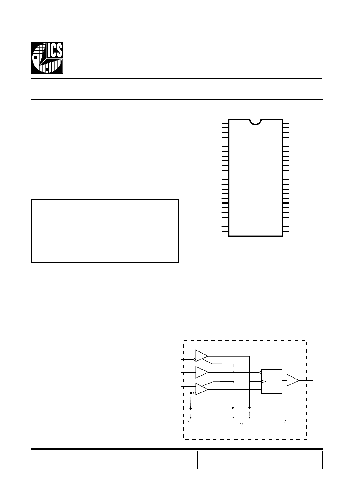
Pin Configuration
Recommended Application:
DDR Memory Modules
Product Features:
• Differential clock signal
• Meets SSTL_2 signal data
• Supports SSTL_2 class I & II specifications
• low-voltage operation
VDD = 2.3V to 2.7V
• 48 pin TSSOP package
DDR 14-Bit Registered Buffer
Truth Table
1
Block Diagram
Q1
Q2
GND
VDDQ
Q3
Q4
Q5
GND
VDDQ
Q6
Q7
VDDQ
GND
Q8
Q9
VDDQ
GND
Q10
Q11
Q12
VDDQ
GND
Q13
Q14
D1
D2
GND
VDD
D3
D4
D5
D6
D7
CLK#
CLK
VDD
GND
VREF
RESET#
D8
D9
D10
D11
D12
VDD
GND
D13
D14
ICSSSTV16857
1
2
3
4
5
6
7
8
9
10
11
12
13
14
15
16
17
18
19
20
21
22
23
24
48
47
46
45
44
43
42
41
40
39
38
37
36
35
34
33
32
31
30
29
28
27
26
25
CLK
CLK#
38
39
48
35
34
D1
VREF
RESET#
To 13 Other Channels
Q1
1
CLK
R
D1
Notes:
1. H = High Signal Level
L = Low Signal Level
↑ = Transition LOW-to-HIGH
↓ = Transition HIGH -to LOW
X = Irrelevant
2. Output level before the indicated
steady state input conditions were
established.
stupnIstuptuOQ
#TESERKLC#KLCDQ
L
roX
gnitaolF
roX
gnitaolF
roX
gnitaolF
L
H
↑↓
HH
H
↑↓
LL
HHroLHroLXQ
0
)2(
48-Pin TSSOP & TVSOP
6.10 mm. Body, 0.50 mm. pitch = TSSOP
4.40 mm. Body, 0.40 mm. pitch = TSSOP (TVSOP)
ICS reserves the right to make changes in the device data identified in
this publication without further notice. ICS advises its customers to
obtain the latest version of all device data to verify that any
information being relied upon by the customer is current and accurate.

2
ICSSSTV16857
Third party brands and names are the property of their respective owners.
General Description
Pin Configuration
The 14-bit ICSSTV16857 is a universal bus driver designed for 2.3V to 2.7V VDD operation and SSTL_2 I/O Levels
except for the RESET# input which is LVCMOS.
Data flow from D to Q is controlled by the differential clock, CLK, CLK# and RESET#. Data is triggered on the
positive edge of CLK. CLK# must be used to maintain noise margins. RESET# must be supported with LVCMOS
levels as VREF may not be stable during power-up. RESET# is asynchronous and is intended for power-up only and
when low assures that all of the registers reset to the Low State, Q outputs are low, and all input receivers, data and
clock are switched off.
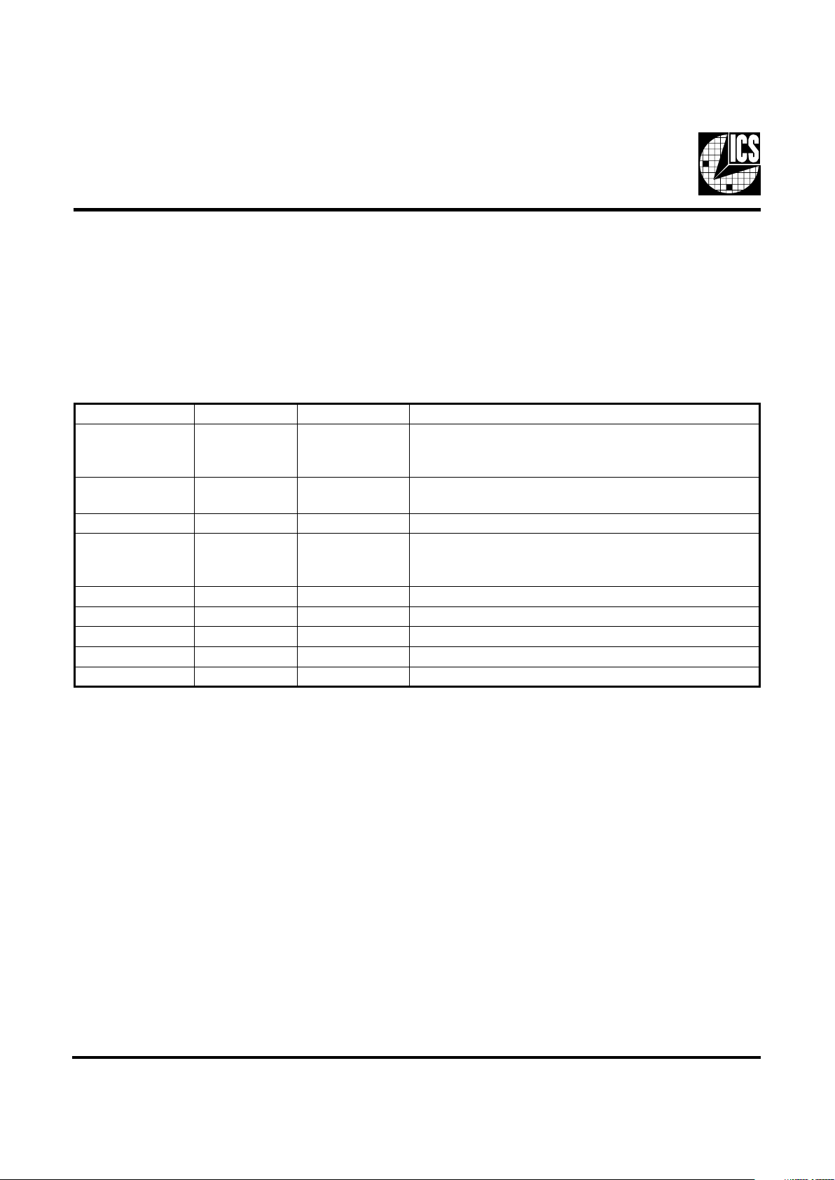
REBMUNNIPEMANNIPEPYTNOITPIRCSED
,81,91,02,32,42
,6,7,01,11,41,51
1,2,5
)1:41(QTUPTUOtuptuoataD
,22,31,8,3
64,63,72
DNGRWPdnuorG
12,61,21,9,4QDDVRWPegatlovylppustuptuO
,13,03,92,62,52
,24,14,04,33,23
84,74,44,34
)1:41(DTUPNItupniataD
83KLCTUPNItupnikcolcevitisoP
93#KLCTUPNItupnikcolcevitageN
54,73,82DDVRWPegatlovylppuseroC
43#TESERTUPNI)wolevitca(teseR
53FERVTUPNIegatlovecnerefertupnI

3
ICSSSTV16857
Third party brands and names are the property of their respective owners.
Absolute Maximum Ratings
Storage Temperature . . . . . . . . . . . . . . . . . . . . . . . –65°C to +150°C
Supply Voltage . . . . . . . . . . . . . . . . . . . . . . . . . . . . -0.5 to 3.6V
Input Voltage
1
. . . . . . . . . . . . . . . . . . . . . . . . . . . . . . . . . . . . . .
-0.5 to VDD +0.5
Output Voltage
1,2
. . . . . . . . . . . . . . . . . . . . . . . . . . . . . . . . . .
-0.5 to VDDQ +0.5
Input Clamp Current . . . . . . . . . . . . . . . . . . . . . . . ±50 mA
Output Clamp Current . . . . . . . . . . . . . . . . . . . . . ±50mA
Continuous Output Current . . . . . . . . . . . . . . . . . ±50mA
VDD, VDDQ or GND Current/Pin . . . . . . . . . . . . ±100mA
Package Thermal Impedance
3
. . . . . . . . . . . . . . . . . . . .
55°C/W
Stresses above those listed under Absolute Maximum Ratings may cause permanent damage to the device. These ratings are
stress specifications only and functional operation of the device at these or any other conditions above those listed in the
operational sections of the specifications is not implied. Exposure to absolute maximum rating conditions for extended
periods may affect product reliability.
Notes:
1. The input and output negative voltage
ratings may be excluded if the input
and output clamp ratings are observed.
2. This current will flow only whtn the
output is in the high state level
V
0 >VDDQ
.
3. The package thermal impedance is
calculated in accordance with
JESD 51.
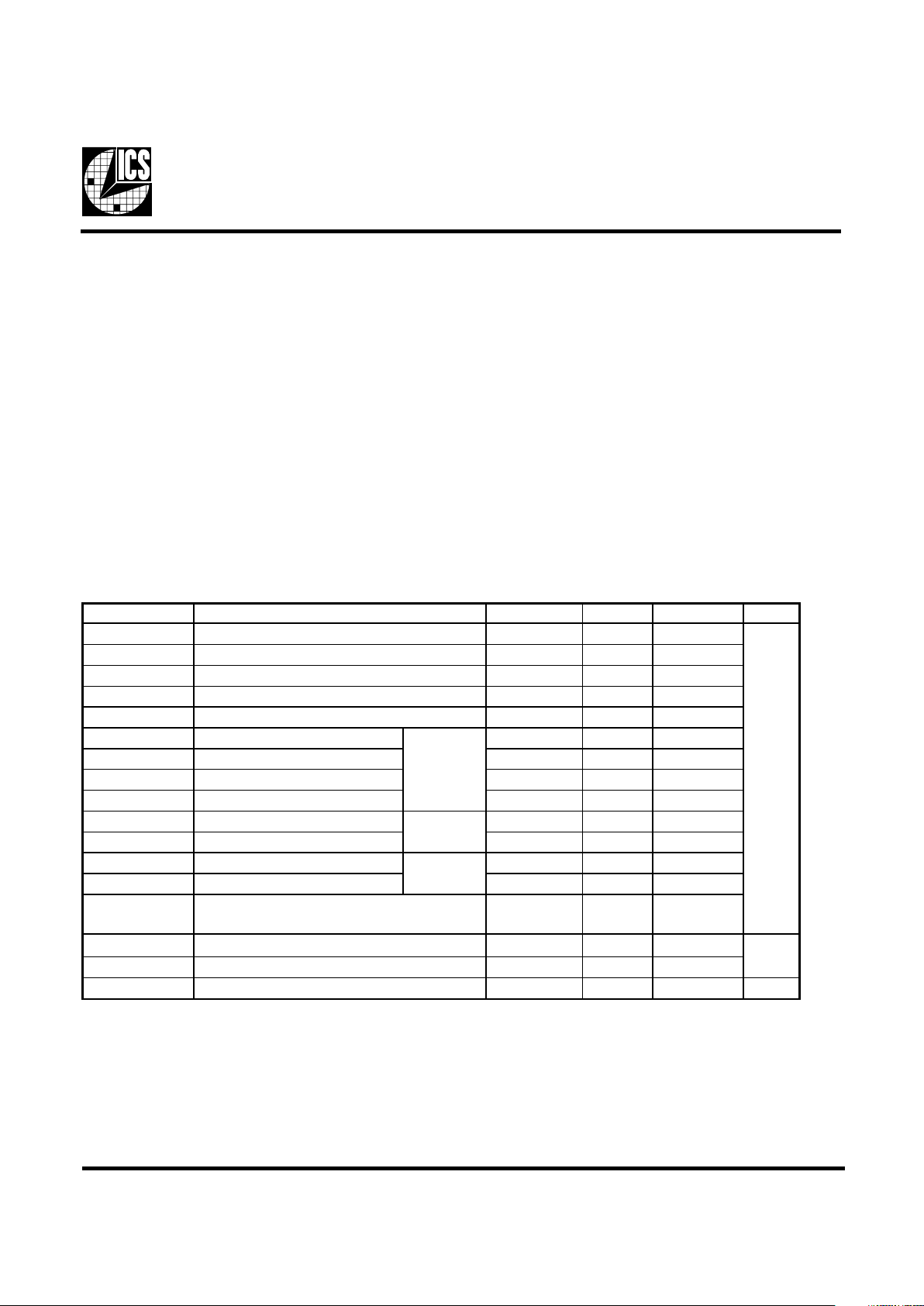
Recommended Operating Conditions
PARAMETER MIN TYP MAX UNITS
V
DD
2.3 2.5 2.7
V
DDQ
2.3 2.5 2.7
V
REF
1.15 1.25 1.35
V
TT
V
REF
-0.04 V
REF
V
REF
-0.04
V
I
Input Voltage 0 V
DD
V
IH
DC Input High Voltage V
REF
+0.15
V
IH
AC Input High Voltage V
REF
+0.31
V
IL
DC Input Low Voltage V
REF
-0.15
V
IL
AC Input Low Voltage V
REF
-0.31
V
IH
Input High Voltage Level 1.7
V
IL
Input Low Voltage Level 0.7
V
ICR
Common mode Input Range 0.97 1.53
V
ID
Differential Input Voltage 0.36
V
IX
(V
DDQ
/2 ) -0.2
(V
DDQ
/2)
+0.2
I
OH
-20
I
OL
20
T
A
070°C
1
Guarenteed by design, not 100% tested in production.
Operating Free-Air Temperature
RESET#
CLK, CLK#
V
Termination Voltage
Cross P oint Voltage of Differential Cloc k
Pair
High-Level Output Current
Low-Level Output Current
Data Inputs
mA
DESCRIPTION
Supply Voltage
I/O Supply Voltage
Reference Voltage V
REF
= 0.5X V
DDQ
 Loading...