ICS507-01/02
PECL Clock Synthesizer
MDS 507 C 1Revision 042600 Printed 11/13/00
Integrated Circuit Systems, Inc. • 525 Race Street • San Jose •CA •95126• (408)295-9800tel • www.icst.com
• Packaged as 16 pin narrow SOIC or die
• Input crystal frequency of 5 - 27 MHz
• Input clock frequency of 5 - 52 MHz
• Uses low-cost crystal
• Differential PECL output clock frequencies up
to 200 MHz
• Duty cycle of 49/51
• 3.3 V or 5.0 V±10% operating supply
• Ideal for SONET applications and oscillator
manufacturers
• Advanced, low power CMOS process
• Industrial temperature versions available
The ICS507-01 and ICS507-02 are inexpensive
ways to generate a low jitter 155.52 MHz (or other
high speed) differential PECL clock output from a
low frequency crystal input. Using Phase-LockedLoop (PLL) techniques, the devices use a standard
fundamental mode crystal to produce output
clocks up to 200 MHz.
Stored in each chip’s ROM is the ability to
generate a selection of different multiples of the
input reference frequency, including an exact
155.52 MHz clock from common crystals. For
lowest jitter and phase noise on a 155.52 MHz
clock, a 19.44 MHz crystal and the x8 selection
can be used.
Description
Features
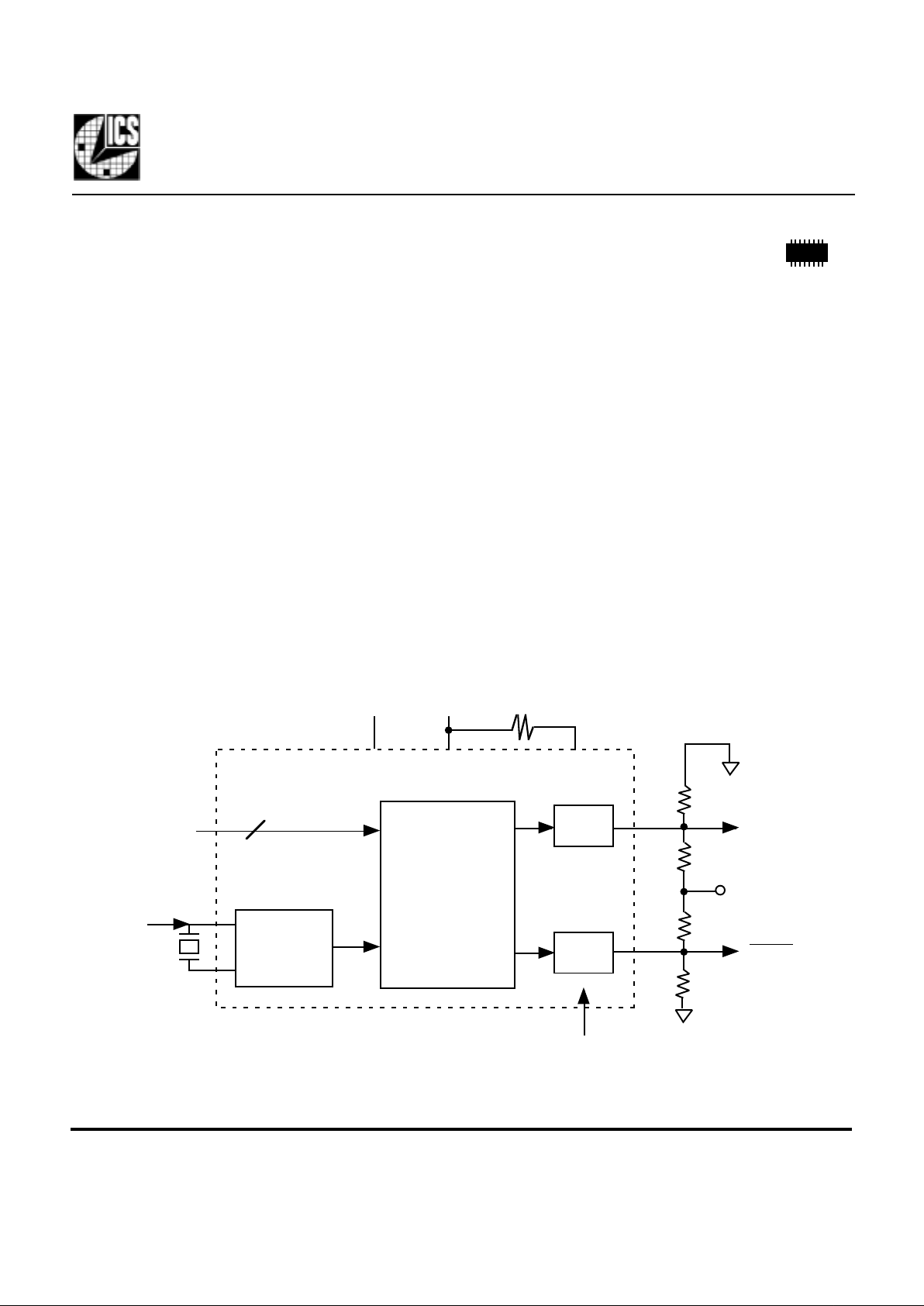
Block Diagram
GND
Crystal
or
clock
X1
X2
S0:1
Output
Buffer
Output
Buffer
PECL
PECL
62Ω
270Ω
270Ω
62Ω
VDD
RES
VDD
1.1kΩ
2
Output Enable
(both out
p
uts)
Output resistor values shown are for unterminated lines.
Refer to MAN09 for additional information.
Clock Synthesis
and Control
Circuitry
Clock
Buffer/
Crystal
Oscillator

ICS507-01/02
PECL Clock Synthesizer
MDS 507 C 2Revision 042600 Printed 11/13/00
Integrated Circuit Systems, Inc. • 525 Race Street • San Jose •CA •95126• (408)295-9800tel • www.icst.com
Pin Assignment
Pin Descriptions
Key: I=Input, O=output, TI=tri-level input, P=power supply connection; XI, XO=crystal connections
Clock Multiplier Select Table
16
15
14
13
16 pin narrow (150 mil) SOIC
12
11
10
9
1
2
3
4
5
6
7
8
ICS507-01/02
VDD
GND
X1/ICLK
VDD
S1
PECL
GND
NC
RES
NC
NC
X2
S0
OE
NC
0 = connect pin directly to ground
1 = connect pin directly to VDD
M = leave unconnected (floating)
PECL
S1 S0 Multiplier
0 0 9.72X*
0 M 10X
0 1 12X
M 0 6.25X
MM 8X
M1 5X
10 2X
1M 3X
11 4X
Number Name Type Description
1 X1/ICLK XI Crystal or clock connection. Connect to a fundamental parallel mode crystal, or clock.
2 VDD P VDD. Connect to +3.3 V or +5 V, and to VDD on pin 3.
3 VDD P VDD. Connect to VDD on pin 2. Decouple with pin 5.
4 S1 TI Multiplier select pin 1. Determines output frequency per table above.
5 GND P Connect to ground.
6 GND P Connect to ground.
7 NC - No connect. Nothing is connected internally to this pin.
8 PECL O PECL Output. Connect to resistor load as shown on page one.
9 PECL O Complementary PECL Output. Connect to resistor load as shown on page one.
10 RES I Bias Resistor Input. Connect a resistor between this pin and VDD.
11 NC - No connect. Nothing is connected internally to this pin.
12 NC - No connect. Nothing is connected internally to this pin.
13 OE I Output Enable. Tri-states both outputs when low. Internal pull-up.
14 S0 TI Multiplier select pin 0. Determines output frequency per table above.
15 NC - No Connect. Nothing is connected internally to this pin.
16 X2 XO Cr stal connection. Connect to cr stal, or leave unconnected for clock input.
*Use this selection to get
155.52 MHz from a 16 MHz
input.
For lowest phase noise
generation of 155.52 MHz,
use a 19.44 MHz crystal and
the 8X selection.
 Loading...