

PRELIMINARY
PRELIMINARY
INFORMATION
INFORMATION
ICS503
LOCO™ PLL Clock Multiplier
Description
The ICS503 is a member of the LOCO™ family,
the most cost effective way to generate a high
quality, high frequency clock output from a low
frequency crystal or clock input. The name LOCO
stands for LOw Cost Oscillator, as it is designed
to replace crystals and crystal oscillators in most
electronic systems. Using Phase-Locked-Loop
(PLL) techniques, the device uses a standard
fundamental mode, inexpensive crystal to produce
output clocks up to 160 MHz.
Stored in the chip’s ROM is the ability to generate
9 different multiplication factors, allowing one
chip to be used in two or three different
applications (see page 2).
Features
• Packaged as 8 pin SOIC or die
• ICS’ lowest cost PLL clock family
• Generates 16.9344 MHz for stereo codecs from
the 14.31818 MHz motherboard clock
• Can be cost effective in replacing a single
surface-mount crystal
• Can be driven by other 5xx series
• Input crystal frequency of 5 - 27 MHz
• Input clock frequency of 2 - 50 MHz
• Output clock frequencies up to 160 MHz
• Low jitter - 50 ps one sigma
• Duty cycle of 45/55 up to 160 MHz
• Operating voltages of 3.0 to 5.5V
• Full CMOS level outputs with 25mA drive
capability at TTL levels
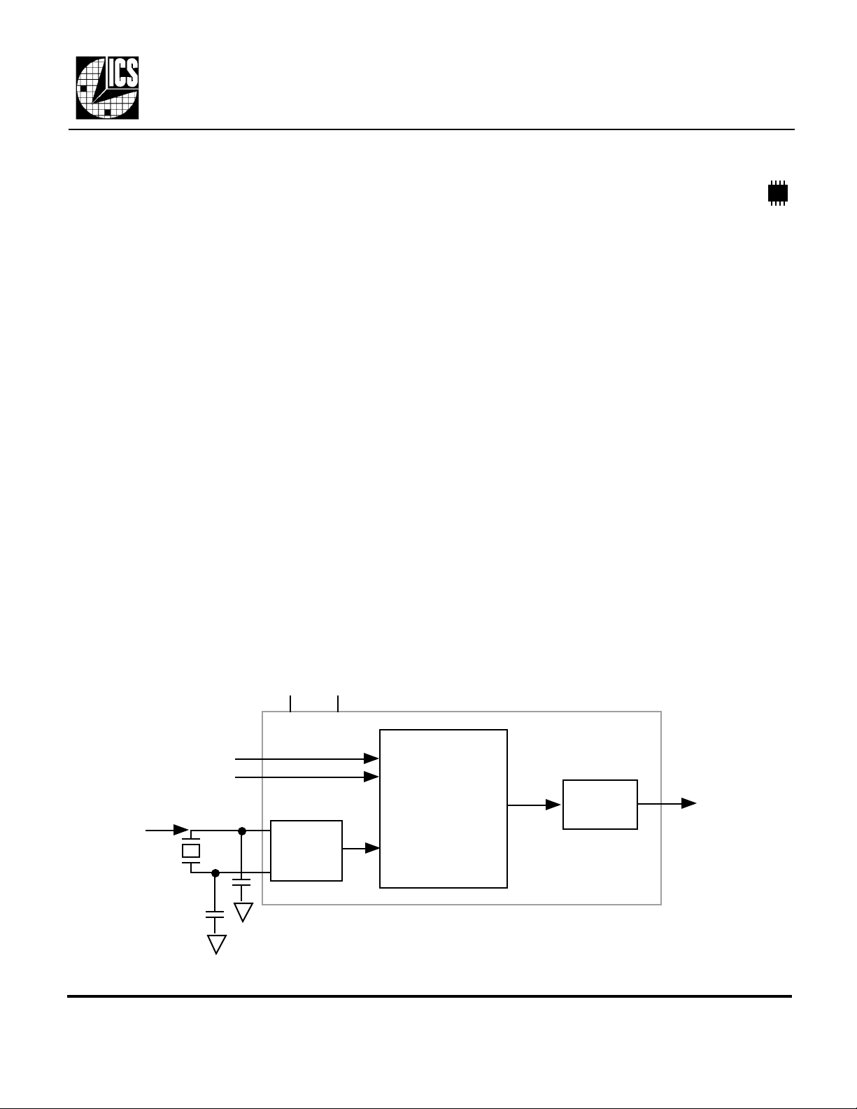
Block Diagram
Crystal or
clock input
S0
S1
X1/ICLK
X2
VDD GND
Clock Multiplier
Crystal
Oscillator
Optional crystal capacitors
• Advanced, low power CMOS process
PLL
Output
Circuitry
and
ROM
Buffer
CLK
MDS 503 A 1 Revision 111000
Integrated Circuit Systems, Inc. • 525 Race Street • San Jose •CA•95126•(408) 295-9800tel • www.icst.com
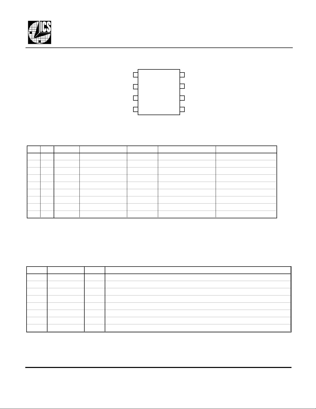
Pin Assignment
PRELIMINARY
PRELIMINARY
INFORMATION
INFORMATION
ICS503
LOCO™ PLL Clock Multiplier
X1/ICLK
VDD
GND
NC
1 8
2
3
4
X2
7
S1
6
S0
5
CLK
Clock Decoding Table (MHz)
S1 S0 Multiplier Typical Input (MHz) CLK (MHz) Input Range (MHz) at 5V Input Range (MHz) at 3.3V
0 0 10 10 100 2 ≤ Input ≤ 16 2 ≤ Input ≤ 10
0 M 16 10 160 2 ≤ Input ≤ 10 2 ≤ Input ≤ 6
0 1 1.1111 27 30.00 20 ≤ Input ≤ 50 20 ≤ Input ≤ 40
M 0 2.4444 14.31818 35.00 10 ≤ Input ≤ 50 10 ≤ Input ≤ 40
M M 2.4164 14.31818 34.60 10 ≤ Input ≤ 50 10 ≤ Input ≤ 40
M 1 2.4 14.31818 34.36 10 ≤ Input ≤ 50 10 ≤ Input ≤ 40
1 0 5.5873 14.31818 80.00 14 ≤ Input ≤ 28 14 ≤ Input ≤ 18
1 M 1.1827 14.31818 16.934 14 ≤ Input ≤ 30 14 ≤ Input ≤ 30
1 1 4.1905 14.31818 60.00 5 ≤ Input ≤ 38 5 ≤ Input ≤ 24
0 = connect directly to ground, 1 = connect directly to VDD, M = leave unconnected (floating).
Pin Descriptions
Number Name Type Description
1 X1/ICLK I Crystal connection or clock input.
2 VDD P Connect to +3.3V or +5V.
3 GND P Connect to ground.
4 NC - Nothing is connected to this pin.
5 CLK O Clock output per Table above. Output frequency equals input frequency times multiplier.
6 S0 TI Select 0 for output clock. Connect to GND or VDD or float.
7 S1 TI Select 1 for output clock. Connect to GND or VDD or float.
8 X2 O Crystal connection. Leave unconnected for clock input.
Key: I = Input, TI = Tri-Level Input, O = output, P = power supply connection
MDS 503 A 2 Revision 111000
Integrated Circuit Systems, Inc. • 525 Race Street • San Jose •CA•95126•(408) 295-9800tel • www.icst.com
 Loading...