

ICS2572RevC090894
Integrated
Circuit
Systems, Inc.
ICS257 2
User-Programmable Dual High-Perform ance Clock Generator
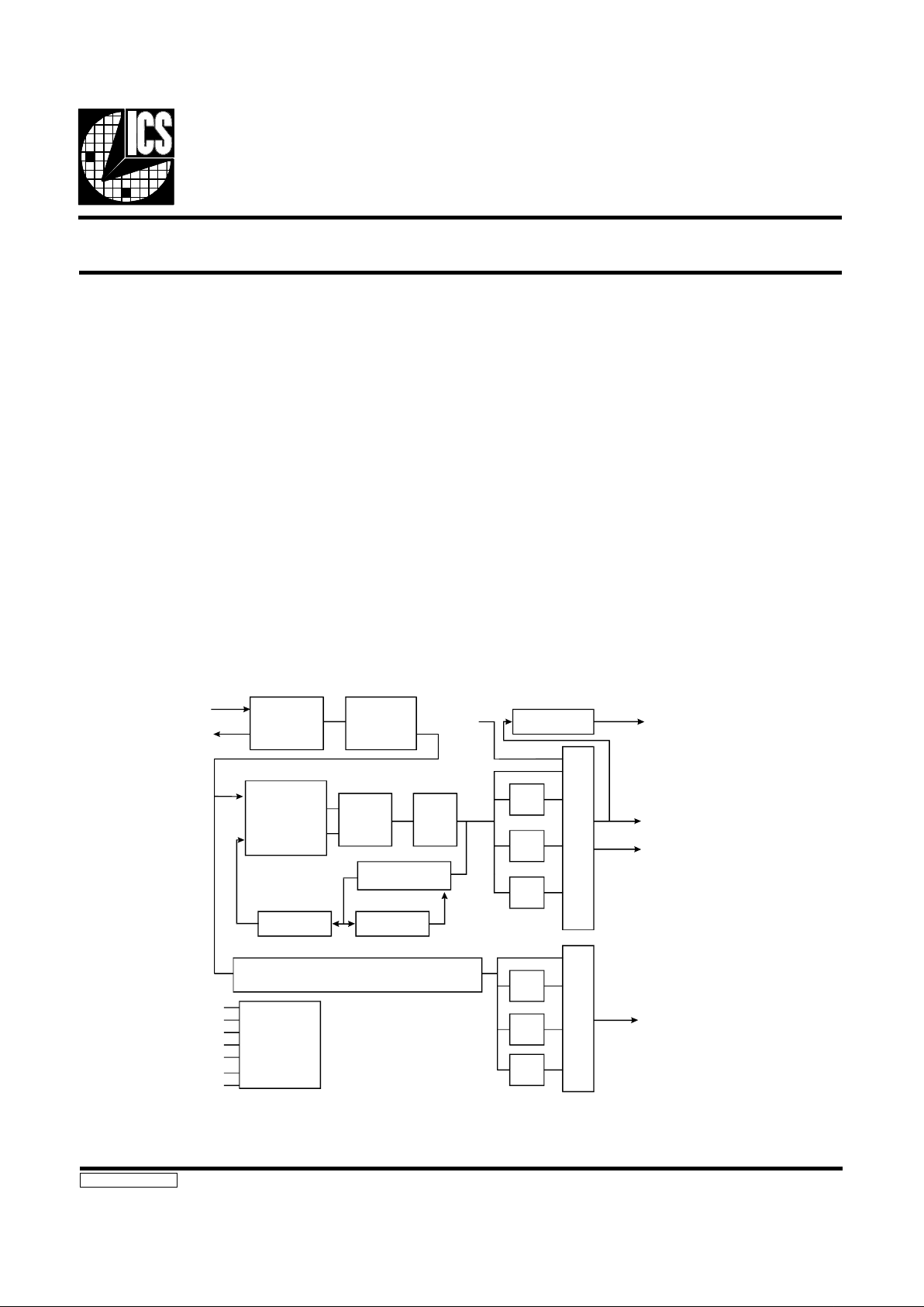
Block Diagram
XTAL1
XTAL2
Crystal
Oscillator
Reference
Divider
Charge
Pump
Phase-
Frequency
Comparator
EXTFREQ
VCO
Prescaler
/M
Strobe
FS0
FS1
FS2
FS3
MS0
MS1
/A
MCLK PLL (as above)
VCLK Set &
Program
Mode
Interface
MCLK Set
/2
/4
/8
/2
/4
MCLK
CLK-
CLK+
LOAD
/1, 4, 5 or 8
/8
Description
The ICS2572 is a dual-PLL (phase-locked loop) clock generator w ith differ ential vi deo outp uts spec ificall y design ed for
high-resolution, high-refresh rate, video applications. The
video PLL generates any of 16 pre-programmed frequencies
through selection of the address lines FS0-FS3. Similarly, the
auxiliary PLL can generate any one of four pre-programmed
frequencies via the MS 0 & MS1 line s.
A unique feature of the ICS2572 is the ability to redefine
frequency selections after power-up. This permits complete
set-up of the fre qu ency table upon system i nit ia l iz a ti on.
Features
•• Advanced ICS mono lithi c phase-l oc ked lo op
technology
•• Supports high-r esolution gr aphics - di fferential CLK out-
put to 185 MH z
•• Div ide d d o tc lock outp ut (L O A D ) a va il a ble
•• Simpl ified device pro gra m mi ng
•• Sixtee n se lect able VC LK fre q uenc ie s (all use r
re-programm able)
•• Four selectable MCLK frequencies (all user
re-programmable)
•• Windows NT compatible
Applications
•• High end PC/low end work sta ti on graphics designs
requiring diffe re ntial outp ut
•• X Termi na l gra ph ic s
E-95
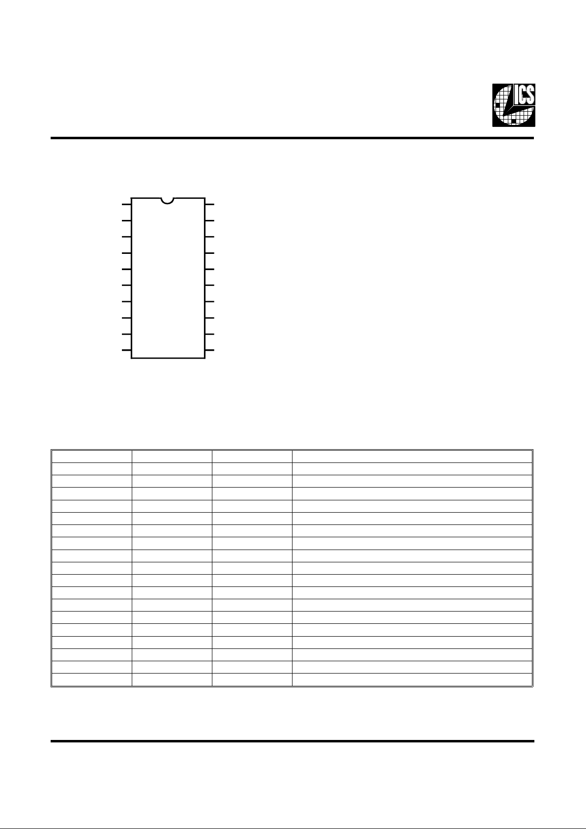
Pin Configuration
XTAL1 1 20 VDD
XTAL2 2 19 CLK+
XTFREQ 3 18 CLK-
FS0 4 17 VSS
FS1 5 16 LOAD
STROBE 6 15 VAA
FS2 7 14 VSS
FS3 8 13 VDD
MS0 9 12 MCLK
VSS 10 11 MS1
ICS2572
Pin Descriptions
PIN NUMBER PIN NAME TYPE DESCRIPTI ON
1 XTAL1 A Quartz crystal connection 1 /Referenc e Frequenc y Input.
2 XTAL2 A Quartz crystal conn ec tion 2.
3 EXTFRE Q I Externa l Fre qu en cy Input
4 FS0 I VCLK PLL Fre que nc y Sele ct LSB.
5 FS1 I VCLK PLL Fre que nc y Sele ct Bit.
7 FS2 I VCLK PLL Fre que nc y Sele ct Bit.
8 FS3 I VCLK PLL Fre que nc y Sele ct MSB.
6 STROBE I Control for Latch of VCLK Se lec t Bits (FS0-FS3).
9 MS0 I MCLK PLL Fre que nc y Sele ct LSB.
11 MS1 I MCLK PLL Fre que nc y Sele ct MSB.
19 CLK+ O Pixel Clock Output (not inverted)
18 CLK- O Pixel Clock Output (inverted)
16 LOAD O Divided Dotcloc k (/4 , 5, or 8)
12 MCLK O MCLK Frequency Output
17 RESERVE D - Must Be Connec t ed to VSS.
10, 14 VSS P Device Ground. All pins mu st be connected.
13, 20 VDD P Output Stage Vdd. All p ins must be conn ec ted .
15 VAA P Synthesizer Vdd.
20-Pin DIP or SOIC
J-4, J-7
ICS2572
E-96
Digital Inputs
The FS0-FS3 pins and the STROBE pin are used to select the
desired operating frequency of the VCLK output from the 16
pre-progr ammed/user -progr ammed select ions in the ICS2572.
These pins are also used to load new frequency data into the
registers.
A vai labl e conf igura tions for the ST ROBE input inclu de: posi tive-e dge triggered, negative-e dge triggered, high-level tra n sparent, and low-level tra nsparent (see Ordering Information).
VCLK Output Frequency Selection
To change the VCLK output frequency, simply write the appropriate data to the ICS2572 FS inputs. Do not perform any
further writes to the device for 50 milliseconds (assumes a
14.318 MHz reference). The synthesizer will output the new
frequency programmed into that location after a brief delay
(see timeout spec ific a tions).
MCLK Output Frequency Selection
The MS0-MS1 pins are used to directly select the desired
operating frequency of the MCLK output from the four preprogrammed/user-programmed selections in the ICS2572.
These inp uts are not latc hed, nor are th ey involve d with me mory programming operations.
Programming Mode Selection
A programmi ng s eq uence is def ined as a p erio d of at l ea s t 5 0
milliseconds of no data writes to the ICS2572 (to clear the shift
register) followed by a series of data writes (as shown here):
FS0 FS1 FS2 FS3
XXSTART bit (must be “0”) 0
XX ” 1
XXR/W* cont rol 0
XX ” 1
XXL0 (location LSB ) 0
XX ” 1
XXL1 0
XX ” 1
XXL2 0
XX ” 1
XXL3 0
XX ” 1
XXL4 (location MSB) 0
XX ” 1
XXN0 (feedba ck LSB) 0
XX ” 1
XXN1 0
XX ” 1
XXN2 0
XX ” 1
XXN3 0
XX ” 1
XXN4 0
XX ” 1
XXN5 0
XX ” 1
XXN6 0
XX ” 1
XXN7 (feedback MSB) 0
XX ” 1
XXEXTFREQ bit (selected if “1”) 0
XX ” 1
XXD0 (post-divide r LSB) 0
XX ” 1
XXD1 (post-divider MSB) 0
XX ” 1
XXSTOP1 bit (mus t be “1” 0
XX ” 1
XXSTOP2 bit (must be “1”) 0
XX ” 1
ICS2572
E-97

Observe that the internal shift register is “clocked” by a transition of FS3 data from “0” to “1.” If an extended se q uence of
register lo ading is to be perform ed (such as a p ower-on initia lization sequenc e), note that it is not necessary to imple ment the
50 millisecond delay between them. Simply repeat the sequence above as many times as desired. Writes to the FS port
will not be treated as frequency select data unti l up to 50
milli second s ha ve tr ansp ired sinc e th e last writ e. No te t hat FS0
and FS1 inputs are “don’ t care. ”
Data Description
Location Bits (L0-L4)
The first five bits after the start bit control the frequency
location to be re-programmed according to this table. The
rightmo st bit (the LSB) of the five shown in each sel e ct ion of
the table is the first one sent.
Table 1 - Location B it Programmi ng
L[4-0] LOCATION
01100 VCLK Address 12
01101 VCLK Address 13
011 10 VCLK Address 14
01111 VCLK Address 15
10010 MCLK Addr ess 2
10011 MCLK Addr ess 3
Feedback Set Bits (N0-N7)
These bits control the feedback divider setting for the location
specified. The modulus of the feedback divider will be equal
to the value of these bits + 257. The least significant bit (N0)
is sent first.
Post-Divider Set Bits (D0-D1)
These bits control the post-divider setting for the location
specified according to thi s table. The lea st signif icant bit (D0)
is sent first.
T able 2 - Post-Divider Programming
D[1-0] POST-DIVIDER
00 9
01 4
10 2
11 1
Read/Write* Control Bit
When set to a “0,” the ICS2572 shift register will transfer its
contents to the selected memory register at the completion of
the progra mm ing sequence out li ne d ab ove .
When th is bi t is a “1 ,” the s elec ted mem or y l oc atio n w il l b e
transferre d to the shift r egister to permit a subsequent re adbac k
of data . No mod ifi c atio n of de vi ce m em ory wil l be p er forme d.
To readback any location of memory, perform a “dummy”
write o f dat a ( co mp lete wit h sta rt a nd st op bits) to that loc atio n
but s et t he R/ W* co ntrol bi t (mak e it “1 ”). A t the end of the
sequence (i.e., after the stop bits have been “clocked”), “clocking” of the FS3 input 11 more times will output the data bits
only in the same sequence as above on t he FS0 pin.
EXTFREQ Input
The EXT FREQ input a llows an e xternally ge nerated fr equency
to be routed to the VCLK output pin under device programming control . If the EXTFREQ bit is set (logic “1”) at the
selected address location (VCLK addresses only), the fre-
quency applied to the EXTFREQ input will be routed to the
VCLK output.
ICS2572
E-98

Frequency Synthesizer Description
Refer to Figure 1 for a block diagram of the ICS2572.
The ICS2572 generates its output frequencies using phase-
locked loop techniques. The phase-locked loop (or PLL) is a
closed-loop feedback system that drives the output frequency
to be ratiometric ally related to the reference frequency provided to the PLL. The phase-frequency detector shown in the
block diagram drives the VCO to a frequency that will cause
the two inputs to the phase-frequency detector to be matched
in freque ncy and phase. This occurs when:
N
F
VCO=FXTAL1
*
2
where N is the eff ective modulus of th e feedbac k divider chain
and R is the modu lus of t he ref er en ce divider chain.
The feedba ck divid er on the ICS2572 m ay be set to any inte ger
value from 2 57 to 512. Th is is done by the sett ing of t he N0- N7
bits. The stan dard refere nce divid er on the ICS2572 is fixed t o
a valu e of 43 (this may be s et to a di fferen t valu e via ROM
programmi ng; conta ct fact ory). The ICS2572 is equi pped wit h
a post-di vider a nd multi plexe r that al lows the output f reque ncy
range to be sca led down f rom that of the VCO b y a fa cto r of 2,
4, or 8.
Therefore, the VCO frequency range will be from 5.976 to
11.906 (257/43 to 512/43) of the reference frequency. The
output frequency range will be from 0.747 to 11.906 times the
reference frequency. Worst case accuracy for any desired frequency within that range will be 0.2%.
If a 14.31818 MHz reference is used, the output frequency
range would be from 10. 69 7 MHz to 170. 48 6 MHz.
Programming Example
Suppose that we want differential CLK output to be
45.723 MHz. We will assume the reference frequency to be
14.31818 MH z .
The VCO frequency range will be 85.565 MHz to
170.486 MHz (5.976 * 14.31818 to 11.906 * 14.31818). We
will need to set the post-divider to two to get an output of
45.723 MHz.
The VCO will then need to be programmed to two times
45.723 MHz, or 91.446 MHz. To calculate the required feedback divider modulus we divide the VCO frequency by the
reference frequenc y a nd m ult iply by the refere nce divide r:
91.446
*43=274.62
14.31818
which we round off to 275. The exact output frequency will
be:
275 1
*14.31818* =45.784 MHz
43 2
The value of the N programming bits may be calculated by
subtracting 257 from the desired feedback divider modulus.
Thus, the N value will be set to 18 (275-257) or 00010010
2
.
The D bit programming is 10
2
(from Table 2).
LOAD Frequency Selection
The L OAD (o r divided dotc lock) output frequency will be the
CLK+/CLK- frequency divided by 1, 4, 5, or 8. The choice of
modulus is a factory option, and is specified along with the
ROM frequencies in the VCLK and MCLK tables by way of
the two-digit suffix of the part num be r.
Reference Oscillator & Crystal
Selection
The ICS2572 has on-board circuitry to implement a Pierce
oscillator with the addition of only one external component, a
quartz cr ysta l. Pier ce osc illa tors opera te the c ry stal in par allel resonant (also called anti-r esonant mode. See the AC Chara cteristics for the effective capacitive loading to specify when
orde ri n g cr ystal s .
Crystals char acter ized for t heir series-re sonant freque ncy ma y
also be used with the ICS2572. Be aware that the oscillation
frequency in circui t wil l be slig htly higher than the freq uency
that is stamped on the can (typ ica ll y 0.025- 0.05% ).
As t he e nt ire op erat io n o f the ph ase -lo ck ed l oop d epen ds on
havin g a st able re ferenc e freq uency, we rec ommend that the
crystal be mo unted a s close ly as p ossible to the pac kage. Avoid
routing digital signals or the ICS2572 outputs underneath or
near these traces. It is also desirable to ground the crystal can
to the ground plan e, if po s sible.
ICS2572
E-99

External Reference Sources
An external frequency source may be used as the reference for
the VCLK and MCLK PLLs. To implement this, simply connect the reference frequency source to the XTAL1 pin of the
ICS2572. For best results, insure that the clock edges are as
clean and fast a s possi ble and that the input volt age threshol ds
are not vi olated.
Power Supply
The ICS2572 has two V SS pins to r educe the effec ts of pac kage
inductance. Both pins are connected to the sam e potential on
the die (the ground bus). BOTH of these pins should connect
to the ground plane of the video board a s close to the package
as is po ssible.
The ICS2572 has a VDD pin which is the supply of +5 volt
power to all out put stage s. Thi s pin shoul d be conne cted t o the
power plane (or bus) using standard high-fr equency decoupling practice. That is, use low-capacitors should have low
series inducta nc e and be m ount ed close to the ICS2572 .
The VAA pin is the power supply for the synthesiz e r circui tr y
and other lowe r curre nt di gi tal fu nc tions. We recommend th at
RC decouplin g or zener regul ati on be prov ided for this pin (a s
shown in the recommended application circuitry). This will
allow the PLL to “track” through power supply fluctuations
withou t vi sible effe c ts.
ICS2572
E-100

Absolute Maximum Ratings
Supply voltage . . . . . . . . . . . . . . . . . . . . . . . . . . . . . . -.5V to +7V
Logic input s . . . . . . . . . . . . . . . . . . . . . . . . . . . . . . . . .-.5V to V
DD
+.5 V
Am b ient operating temp. . . . . . . . . . . . . . . . . . . . . . . 0 to 70°C
Storage temperature . . . . . . . . . . . . . . . . . . . . . . . . . . -85 to + 150°C
Stresses abov e those listed unde r Absol ute Ma ximum Rat ings m ay c ause p er mane nt da mag e to t he devi ce. Th is is a stre ss rat ing
only and functio na l ope ra ti on of the devi ce at these or a ny oth er cond itions above those indic a ted in th e opera t ion al sec tions o f
the specifications is not implied. Exposure to absolute maximum rating conditions for extended periods may affect product
reliability.
DC Characteristics
PARAMETER SYMBOL TEST CONDITIONS MIN TYP MAX UNITS
TTL-Compatible Inputs - - (FS0-3, MS0-1, STROBE): - - -
Input High Voltage V
ih
2.0 - VDD+0.5 V
Input Low Voltage V
il
VSS-0.5 - 0.8 V
Input High Current I
ih
--10uA
Input Low Current I
il
- - 200 uA
Input Capacitan ce C
in
--8pF
XTAL1: - - -
Input High Voltage Vx h VDD*0.75 - VDD+0.5 V
Input Low Voltage Vxl VSS-0.5 - VDD*0.25 V
CLK+/CL K- Out put
Sink Current
Isink - - - mA
High Voltage ( Other
Outputs)
Voh 4 - - V
@Ioh=0.4mA - - -
Low Voltage (Oth er
Outputs)
Vol - - 0 .4 V
@Iol=8.0mA - - -
ICS2572
E-101

AC Characteristics
PARAMETER SYMBOL TEST CONDITIONS MIN TYP MAX UNITS
Phase-Locked Loop : - - -
VCLK, MCLK VCO
Frequenc y
Fvco 100 - 235 MHz
PLL Ac quire T i m e T loc k - 5 00 - uSec
Crystal Oscillator - - -
Crystal Frequency
Range
Fxtal 5 - 25 MHz
Para llel Loading
Capacitance
-20-pF
XTAL1 Minimum High
Time
Txhi 8 - - ns
XTAL1 Minimum Low
Time
Txlo 8 - - ns
Power Supplies: - - - -
VDD Supply Current idd - - 35 mA
VAA Suppl y Current Iaa - - 10 mA
Digital Outputs: - - -
CLK+/CLK- Recommended Termination
50 - 2 ohms
Other Output s Rise
Tim e @ Cl oa d=20pF
Tf - - 2 ns
Other Outpu ts Fa ll Time
@ Cload= 20 p F
Tf - - - ns
ICS2572
E-102

PATTERN ICS2572-01
Reference Divider 43
VCLK ADDR FbkDiv/PostDiv - F
VCLK
(MHz)
0 300/ 1- 99.89
1 378/1 - 125.87
2 277/1 - 92.24
3 432/4 - 35.96
4 302/2 - 50.28
5 340/2 - 56.61
6 EXTFREQ7 270/2 - 44.95
8 405/1 - 134.86
9 384/4 - 31.97
A 330/1 - 109.88
B 481/2 - 80.08
C 479/4 - 39.87
D 270/2 - 44.95
E 450/2 - 74.92
F 390/2 - 64.93
MCLK ADDR FbkDiv/PostDiv - F
MCLK
0 481/4 - 40.04
1 270/2 - 44.95
2 396/4 - 32.97
3 300/2 - 49.95
Ordering Information
ICS2572N-SXX or ICS2572M-SXX (0.300" DIP o r SOIC Packag e)
Example:
ICS XXXX N-SXX
S=Strobe Option/XX=Default Frequencies
Package Type
N=DIP (Plastic)
M=SOIC
Device Type (consists of 3 or 4 digit numbe rs )
Prefix
ICS, AV=Standard Device; GSP=Genlock Device
Where:
“s” denot e s strobe option : A - positive leve l transparen t (i.e., 2494 i nterface co mpatible)
“xx” de not es de fault frequenci e s: B - negati ve le ve l tr an sp arent
C - positive edge triggered
D - negative edge triggered
ICS2572
E-103

NOTES
ICS2572
E-104
 Loading...