

Page 1

NOVA-4898-R3
Low Power GXLV/GX1
MMX with SVGA/LCD,
Ethernet, & Audio SBC.
PCB Version 3.3
User Manual
Version 3.3
August 8, 2003
©Copyright 2003 by ICP Electronics Inc. All Rights Reserved.
Page 2

Copyright Notice
The information in this document is subject to change without prior notice
in order to improve reliability, design and function and does not represent a
commitment on the part of the manufacturer.
In no event will the manufacturer be liable for direct, indirect, special,
incidental, or consequential damages arising out of the use or inability to
use the product or documentation, even if advised of the possibility of such
damages.
This document contains proprietary information protected by copyright. All
rights are reserved. No part of this manual may be reproduced by any
mechanical, electronic, or other means in any form without prior written
permission of the manufacturer.
Trademarks
NOVA-4898 is a registered trademark of ICP Electronics Inc. IBM PC is a
registered trademark of International Business Machines Corporation. Intel
is a registered trademark of Intel Corporation. Other product names
mentioned herein are used for identification purposes only and may be
trademarks and/or registered trademarks of their respective companies
2
Page 3

Table of Contents
1. INTRODUCTION ........................................... 4
1.1 SPECIFICATIONS.................................................................5
1.2 PACKAGE CONTENTS............................................................7
2. INSTALLATION............................................. 8
2.1 NOVA-4898 BLOCK DIAGRAM & BOARD LAYOUT .........................8
2.2 UNPACKING PRECAUTIONS ...................................................10
2.3 COMPACT FLASH SETTING (JP3)............................................ 10
2.4 WATCH DOG TIMER SETTING .................................................10
2.5 CLEAR CMOS SETUP .........................................................11
2.6 COM2 SETTING JP11, JP12 , JP13 ...................................... 11
2.7 LCD VOLTAGE SELECTOR ....................................................12
2.8 DISKONCHIP™ FLASH DISK MEMORY ADDRESS SETTING...............13
3. CONNECTION.............................................. 14
3.1 FLOPPY DISK DRIVE CONNECTOR (CN10) ................................ 14
3.2 PCI E-IDE DISK DRIVE CONNECTOR (CN3,CN4) ......................15
3.3 PARALLEL PORT (CN11) .....................................................16
3.4 SERIAL PORTS (CN16, CN17, CN18, CN19) ..........................17
3.5 AUDIO CONNECTOR ...........................................................18
3.6 KEYBOARD & PS/2 MOUSE CONNECTOR (CN13)........................ 19
3.7 USB PORT CONNECTOR CN5 ...............................................20
3.8 IRDA INFRARED INTERFACE PORT (CN6) .................................20
3.9 VGA CONNECTOR (CN23) .................................................. 21
3.10 LCD INTERFACE CONNECTOR ..............................................21
3.11 LAN RJ45 CONNECTOR AND ETHERNET LED ...........................23
1
Page 4

3.12 EXTERNAL SWITCHES AND INDICATORS (JP15)......................... 23
3.13 EXTERNAL POWER CONNECTOR ............................................24
3.14 PC/104 CONNECTION BUS ................................................ 24
3.15 DIGITAL I/O (CN12) ......................................................26
3.16 TV-OUT (CN22, CN24) .................................................27
4. AWARD BIOS SETUP ................................. 28
4.1 GETTING START ...............................................................28
4.2 STANDARD CMOS SETUP.................................................... 29
4.3 BIOS FEATURES SETUP...................................................... 30
4.4 CHIPSET FEATURES SETUP ...................................................31
4.5 POWER MANAGEMENT SETUP ................................................31
4.6 PNP / PCI CONFIGURATION ............................................32
4.7 LOAD BIOS DEFAULTS ...................................................33
4.8 LOAD SETUP DEFAULTS ................................................. 34
4.9 INTEGRATED PERIPHERALS ............................................34
4.10 PASSWORD SETTING...................................................36
4.11 IDE HDD AUTODETECTION ...........................................36
4.12 SAVE AND EXIT SETUP.................................................37
4.13 QUIT WITHOUT SAVING ....................................................38
5. SVGA SETUP................................................ 39
5.1 INTRODUCTION ................................................................ 39
5.2 FURTHER INFORMATION ......................................................40
6. AUDIO .......................................................... 41
6.1 INTRODUCTION ................................................................ 41
7. PCI BUS ETHERNET INTERFACE ............. 42
7.1 INTRODUCTION ................................................................ 42
2
Page 5

APPENDIX A. WATCHDOG TIMER ............... 43
APPENDIX B. I/O ADDRESS MAP................ 46
B.1 SYSTEM I/O ADDRESS MAP .................................................46
B.2 DMA CHANNEL ASSIGNMENTS ..............................................47
B.3 INTERRUPT ASSIGNMENTS.................................................... 47
ST
B.4 1
MB MEMORY MAP .........................................................48
3
Page 6

1. Introduction
NOVA-4898 is designed for limited space applications with only
the size of a 5 1/4 " hard drive. It supports the full functions of an
AT& ATX-compatible industrial computer on a single board. The
NOVA-4898 is equipped with a low-power consumption and high
performance GX1 processor on board. It also contains an SDRAM
DIMM socket that can support up to 512 MB memory.
The NOVA-4898 provides an Ethernet interface, audio interface,
and socket for DiskOnChip, EIDE interface, one parallel port, three
RS-232 serial ports, one RS-232/422/485 serial port with
auto-direction, and a PS/2 keyboard/mouse interface. The built-in
SVGA/LCD display controller supports both the CRT and LCD display
simultaneously. It offers the resolutions of LCD screen up to 800 x
600 and CRT resolutions up to 1280 x 1024 @ 256 colors &1024x
768 @ 16 bpp. It also provides TV-OUT interface for PAL or NTSC TV.
The display type is configured through software utility. The Flash
ROM contains both the system BIOS and the VGA BIOS. If
necessary, reprogramming the Flash ROM allows modifications.
The RS485 has an outstanding feature of intelligent directing
control, which eliminates the extra control signal such as RTS. With
this feature you can develop your program using your normal RS232,
no need to change to a special control routine. This feature is
especially important in WINDOWS programming where the program
do not allow you to catch the control pin freely.
Finally, one PC/104 connector and one PCI slots are included for
the future application that might come in handy.
4
Page 7

1.1 Specifications
NS GX1-233/266/300 MMX 32-Bit x86 Processor:
Supports Intel MMX instruction set extension for the
acceleration of multi media applications
16 KB unified L1 cache
Five-stage pipelined integer unit
Integrated Floating Point Unit(FPU)
System memory: One 168-pin DIMM socket support up
to 512MB SDRAM
BIOS: AWARD 256 KB Flash memory
Display Controller:
MediaGx processor has implemented the UMA
technology that provides 1.5~4MB display memory,
setup through BIOS Setup Menu.
Support CRT and TFT LCD displays simultaneously
Support 18-bit TFT LCD panel resolution up to
800x600 @ 18bpp
Support non-interlaced CRT monitors resolutions up
to 1280x1024 @ 256 colors &1024x768 @ 16bpp
Audio:
Compliant to AC97, support stereo
Connector: Speaker, Mic-in, Line-in, Line-out, CD-in
TV-OUT: Support both NTSC and PAL.
IDE interface: The IDE support to four PCI Enhanced IDE
hard drives
FDD interface: Support up to two floppy disk drives,
5.25”(360KB and 1.2MB)and/or 3.5”(720KB, 1.44MB, and
2.88MB)
Serial ports: four RS232 ports, one RS232 port can be
set to RS-422/485 with Self-Tuner technology or can be
set to infrared port with Transfer rate up to 115 KBPS
Parallel port: One Parallel port, supports SPP/EPP/ECP
mode
5
Page 8

PS/2 Mouse/Keyboard connector: A 6-pin connector
for easy connection to a keyboard or PS/2 mouse
USB interface: Two USB ports, USB 1.0 compliant
Power management: supports power saving modes
including Normal/Doze/Sleep modes. APM1.1 compliant
Watchdog timer: can be set by 1-255 seconds period.
Reset or NMI was generated when CPU did not periodically
trigger the timer.
10/100Mbps Ethernet Controller: Intel 82559,82551,or
Realtek RTL8100BL IEEE802.u 100 BASE-TX standard Dual
Auto -sensing interface to 10MBps or 100MBps networks.
On board RJ45 connectors provide for easy connection.
DiskOnChip
TM
Flash Disk: supports one 32-pin socket for
DiskOnChip Flash Disk
CompactFlash Disk: The CompactFlash Storage Card
also runs in True IDE Mode that is compatible with an IDE
disk drive. It can be used with a passive adapter in a Type
II socket.
Expansion bus: one PC/104 and one PCI slot
Power supply: +5V @1.8A ( typical ) ,+12V @50mA
( typical ) Power supply can use 5V only , +5V @2.0A
(typical)
Operating temperature: -10~60℃
Dimension: 8”(L)x5.75”(W)(203mmx146mm)
6
Page 9

1.2 Package Contents
Before you begin installing the product, please check that all of
the following listed materials are included in the package:
• 1 NOVA-4898 All-in-one single board computer
• 1 CD disk for utility and drivers
• 1 3.5" IDE flat cable (40-pin to 40-pin 2.54mm pitch)
• 1 standard D25 connector for parallel cable (Printer)
• 3 serial port flat cable (RS-232 , 2.54mm pitch)
• 1 combo serial port cable (RS-232/422/485 , 2.54mm pitch)
• 1 floppy cable (for 3.5" FDD only)
• 1 2.5" IDE flat cable (44-pin to 44-pin 2.0mm pitch)
• 1 VGA ROUND CABLE(10 pin to D-SUB 15 pin)
• 1 one to two 6pin mini Din Connector for keyboard and
mouse
• 1 audio cable sets •
• 1 TV AV cable •
• 1 LCD 44 Pin Connector (FP24-01A)•
If any of these items are missing or damaged, please contact
your distributor or sales representative immediately.
7
Page 10
2. Installation
This chapter gives you a step-by-step guidance as to install NOVA-4898
hardware, including directions on how to configure the setting for jumpers and
connecting peripherals, switches and indicators. Before installation, please
pay attention to the unpacking precautions on the following page for safety.
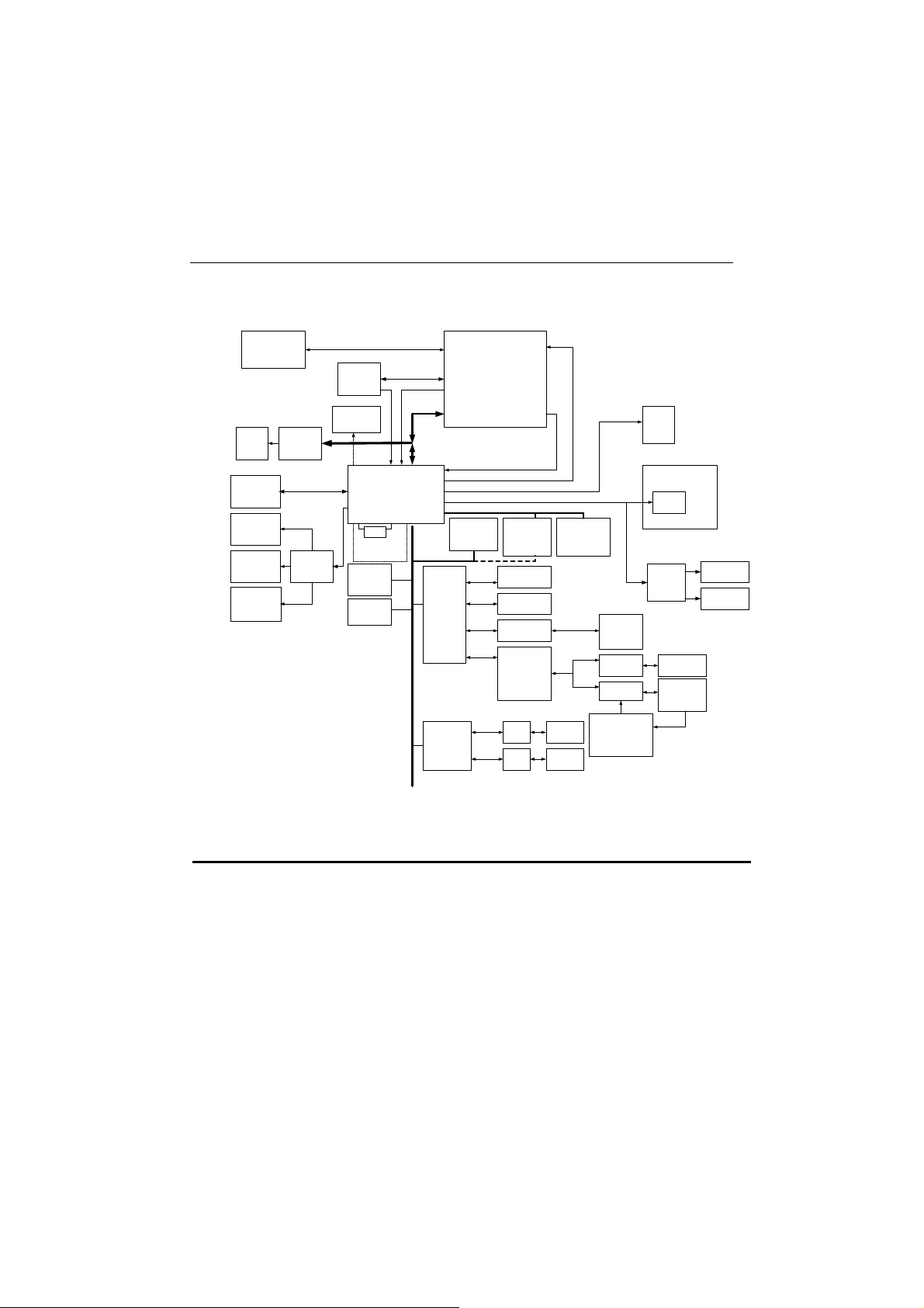
2.1 NOVA-4898 Block Diagram & Board Layout
SDRAM
1 x DIMM
Socket
CN14/
CN8
RJ45
CN5
USB
( 2 Ports )
CN2
Sspeakers
CD-IN
CD ROM
Audio
CN2
Microphone
Intel
82551/
8100BL
AC97
CODEC
AD1881A
MD [ 63:0 ]
Clocks
System
Clocks
MHz Crystal
Socket
DOC
WDT
CS5530
I/O Companion
14.31818
U14
RAM YUV Port
Por ( Video )
MediaGX
MMX-TMEnhanced
Processor
Serial
Packet
RGB Port
( Graphics )
PCI Bus
Graphics Data
Video Data
Analog Rgb
IDE Control
Award
BIOS
Super I/O
83977F-A
Winbond
Second
83877
Windboand
2Mb
ISA Bus
FDD
Printer
COM1
COM2
COM3
COM4
TM
CN23
VGA
CRT
TFT Panel
CN1
CN3
Primary
IDE
Devices
CN10
FDD
CN11
Printer
MAX
213
JP11
JP13
RS-232/
422/485
Selector
MAX
213
MAX
213
Second IDE
Devices
CN17
COM13
CN16
COM4
CN4
COM1
RS-232
CN18
MAX
213
LTC1487
Selftuner
intelligent
directing
Control
TV-OUT
CH7003
RS-232
RS-422
RS-485
CN19
CN19
CN24
S-VIDEO
CN22
AV-VIDEO
8
Page 11

9
Page 12
2.2 Unpacking Precautions
Some components of NOVA-4898 SBC are very sensitive to
static electric charges and can be damaged by a sudden rush of
power. To protect it from unintended damage, be sure to note
these precautions:
Ground yourself to remove any static charge before
touching the NOVA-4898 SBC. You can do it by using a
grounded wrist strap at all times or by frequently touching
any conducting materials that is connected to the ground.
Handle your NOVA-4898 SBC by its edges. If not necessary,
don’t touch IC chips, leads or circuitry.
Do not plug any connector or jumper while the power is on.
There is one 168-pin DIMM socket that accept 3.3V
non-buffered SDRAM. The max. Memory size is 512MB.
2.3 Compact Flash Setting (JP3)
Set the operating mode of CompactFlash disk
• JP3 : Compact Flash Setting
Address
MASTER CLOSE
SLAVE OPEN
JP3
2.4 Watchdog Timer Setting
Reading port 443H enables the Watchdog Timer. It should be
triggered before the time-out period ends, otherwise it will
assume the program operation is abnormal and will issue a reset
signal to start again, or activate NMI to CPU. Reading port
043/843H disables the Watchdog Timer. For detail information
about Watch-Dog Timer Refer to Appendix A
10
Page 13

• JP14 : Watchdog Active Type Setting
JP14
1-2 Activate NMI to CPU when WDT time-out
2-3 Reset when WDT time-out
OPEN Disable WDT
DESCRIPTION
2.5 Clear CMOS Setup
If you need to clear the CMOS Setup (for example when you forget the
password, you should first clear the CMOS setup and then reset the
password), you should close JP9 for about 3 seconds, then open it again.
To set back to normal operation mode, please open JP9.
• JP9: Clear CMOS Setup (Reserve Function)
JP9 DESCRIPTION
1-2 Normal Operation
2-3 Clear CMOS Setup
2.6 COM2 Setting JP11, JP12 , JP13
The COM2 (CN19) can supply +5V or +12V power to the serial
devices via RI pin (Pin 8) of the COM port connector. The
maximum electric current is 1A with fuse protection leading
from these two connector’s 5V/12V output. If the output is set
to 12V, make sure that you have 12V power supply connected to
the board.
CN19 Pin 8 JP11 JP12
RI Signal 2-3 Disregard
+5V 1-2 2-3
+12V 1-2 1-2
11
Page 14
COM2 RS-232, RS-422 or RS-485 Setting JP13
The COM2 (CN19) can be set to RS-232 or RS-422/485 for
industrial field site application. Moreover when this port is set to
RS-485 mode the board equipped self-tuner IC will automatically
sense the data direction to eliminate data collision. This feature
is particularly important in WINDOWS programming where the
program do not allow you to catch the control pin freely.
JP13 DESCRIPTION
1-2 RS232
2-3 RS422/RS485
2.7 LCD Voltage Selector
The LCD interface connector CN1 can provide 5V or 3.3V power
supply by selecting the JP1 to meet the different LCD
requirement.
JP1 DESCRIPTION
1-2 5V
2-3 3.3V
JP2: LCD CLOCK Setting
JP2 DESCRIPTION
1-2 Normal
2-3 Inverse
12
Page 15

2.8 DiskOnChip™ Flash Disk Memory Address
Setting
The DiskOnChip™ Flash Disk Chip (DOC) is manufactured by
M-Systems. As the DOC is 100% compatible to hard disk so
DOS Customer doesn‘t need to install any extra software utility.
The “Plug and play” feature is both easy and reliable. Right now
DOC is available from 2MB to 144MB.The MD-2200-Xmb
series DOC will share only 8KB memory address.
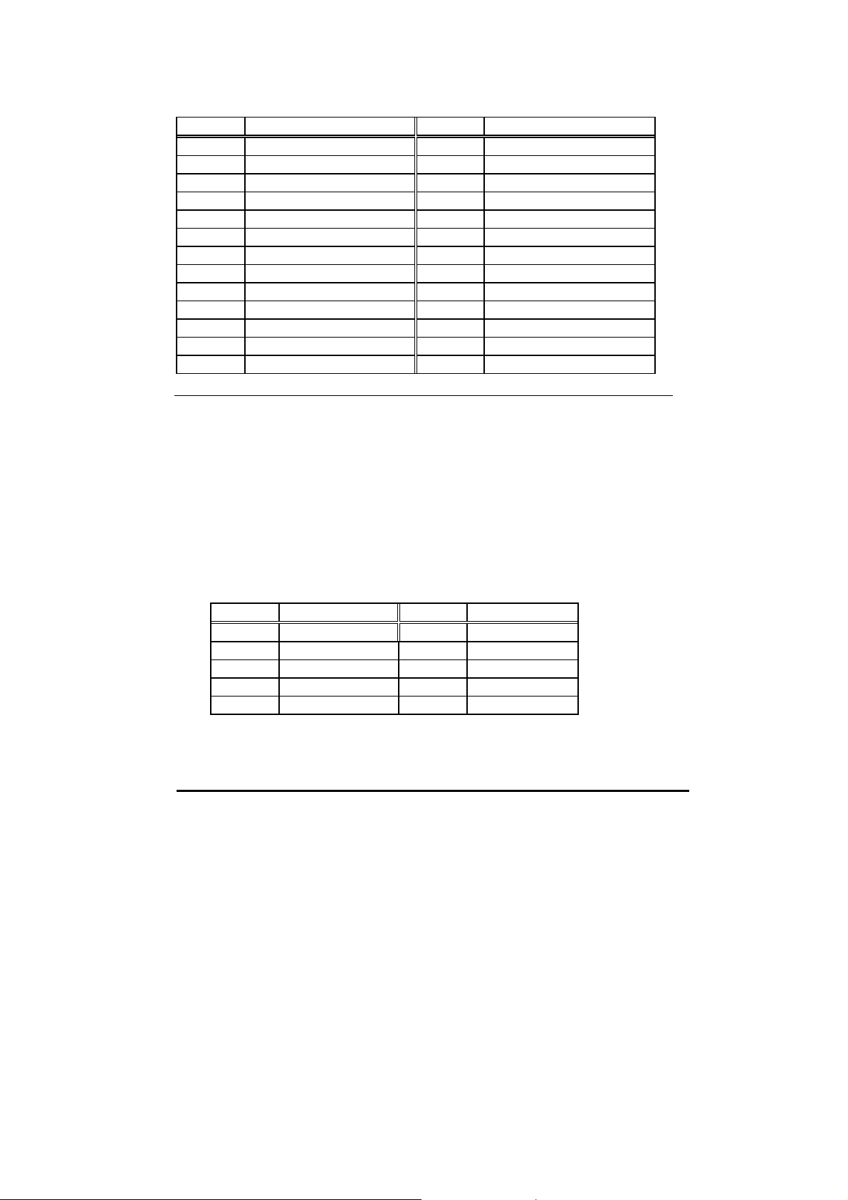
• JP7 & JP8: DiskOnChip Memory Address Setting
ADDRESS
CC000 OPEN OPEN CLOSE OPEN OPEN CLOSE CLOSE
CE000 OPEN OPEN OPEN CLOSE OPEN CLOSE CLOSE
D0000 CLOSE OPEN OPEN OPEN CLOSE OPEN CLOSE
D2000 OPEN CLOSE OPEN OPEN CLOSE OPEN CLOSE
D4000 OPEN OPEN CLOSE OPEN CLOSE OPEN CLOSE
D6000 OPEN OPEN OPEN CLOSE CLOSE OPEN CLOSE
D8000 CLOSE OPEN OPEN OPEN OPEN OPEN CLOSE
DA000 OPEN CLOSE OPEN OPEN OPEN OPEN CLOSE
DC000 OPEN OPEN CLOSE OPEN OPEN OPEN CLOSE
DE000 OPEN OPEN OPEN CLOSE OPEN OPEN CLOSE
1-2 3-4 5-6 7-8 1-2 3-4 5-6
JP8 JP7
13
Page 16

3. Connection
In this chapter, you can find a detailed guide on how to connect
peripherals, switches and indicators to the NOVA-4898 board.
3.1 Floppy Disk Drive Connector (CN10)
NOVA-4898 board is equipped with a 34-pin daisy-chain driver
connector cable.
CN10: FDC CONNECTOR
PIN NO. DESCRIPTION PIN NO. DESCRIPTION
1 GROUND 2 REDUCE WRITE
3 GROUND 4 N/C
5 GROUND 6 N/C
7 GROUND 8 INDEX#
9 GROUND 10 MOTOR ENABLE A#
11 GROUND 12 DRIVE SELECT B#
13 GROUND 14 DRIVE SELECT A#
15 GROUND 16 MOTOR ENABLE B#
17 GROUND 18 DIRECTION#
19 GROUND 20 STEP#
21 GROUND 22 WRITE DATA#
23 GROUND 24 WRITE GATE#
25 GROUND 26 TRACK 0#
27 GROUND 28 WRITE PROTECT#
29 GROUND 30 READ DATA#
31 GROUND 32 SIDE 1 SELECT#
33 GROUND 34 DISK CHANGE#
14
Page 17

3.2 PCI E-IDE Disk Drive Connector (CN3,CN4)
For IDE HDD connection, The NOVA-4898 was designed with
one 2.54mm connector (CN3) & one 2.0mm connector (CN4),
which could be converted to two 2.54mm standard IDE
connector via proprietary cable. Using these cables you can
attach up to four IDE hard disk drives to the NOVA-4898.
CN3: 40-pin Primary IDE Interface Connector
PIN NO. DESCRIPTION PIN NO. DESCRIPTION
1 RESET# 2 GROUND
3 DATA 7 4 DATA 8
5 DATA 6 6 DATA 9
7 DATA 5 8 DATA 10
9 DATA 4 10 DATA 11
11 DATA 3 12 DATA 12
13 DATA 2 14 DATA 13
15 DATA 1 16 DATA 14
17 DATA 0 18 DATA 15
19 GROUND 20 N/C
21 IDE DRQ 22 GROUND
23 IOW# 24 GROUND
25 IOR# 26 GROUND
27 IDE CHRDY 28 GROUND
29 IDE DACK 30 GROUND–DEFAULT
31 INTERRUPT 32 N/C
33 SA1 34 N/C
35 SA0 36 SA2
37 HDC CS0# 38 HDC CS1#
39 HDD ACTIVE# 40 GROUND
15
Page 18

CN4: 44-pin Secondary Mini-pitched IDE Interface
Connector
PIN NO. DESCRIPTION PIN NO. DESCRIPTION
1 RESET# 2 GROUND
3 DATA 7 4 DATA 8
5 DATA 6 6 DATA 9
7 DATA 5 8 DATA 10
9 DATA 4 10 DATA 11
11 DATA 3 12 DATA 12
13 DATA 2 14 DATA 13
15 DATA 1 16 DATA 14
17 DATA 0 18 DATA 15
19 GROUND 20 N/C
21 IDE DRQ 22 GROUND
23 IOW# 24 GROUND
25 IOR# 26 GROUND
27 IDE CHRDY 28 GROUND
29 IDE DACK 30 GROUND–DEFAULT
31 INTERRUPT 32 N/C
33 SA1 34 N/C
35 SA0 36 SA2
37 HDC CS0# 38 HDC CS1#
39 HDD ACTIVE# 40 GROUND
41 VCC 42 VCC
43 GROUND 44 N/C
3.3 Parallel Port (CN11)
This port is usually connected to a printer; The NOVA-4898
includes an on-board parallel port (CN11) that is accessed
through a 26-pin flat-cable connector.
16
Page 19
CN11: Parallel Port Connector
PIN NO. DESCRIPTION PIN NO. DESCRIPTION
1 STROBE# 2 DATA 0
3 DATA 1 4 DATA 2
5 DATA 3 6 DATA 4
7 DATA 5 8 DATA 6
9 DATA 7 10 ACKNOWLEDGE
11 BUSY 12 PAPER EMPTY
13 PRINTER SELECT 14 AUTO FORM FEED #
15 ERROR# 16 INITIALIZE
17 PRINTER SELECT LN# 18 GROUND
19 GROUND 20 GROUND
21 GROUND 22 GROUND
23 GROUND 24 GROUND
25 GROUND 26 N/C
3.4 Serial Ports (CN16, CN17, CN18, CN19)
The NOVA-4898 offers four high speeds NS16C550 compatible
UARTs with Read/Receive 16 byte FIFO serial ports. These ports
let you connect to serial devices or a communication network.
Three 10-pin headers and one 14-pin header are provided. For
detailed pin assignment of the these connectors please refer to
the following tables:
CN18 (com1), Serial Port (10-pin Header/W Housing)
PIN NO. DESCRIPTION PIN NO. DESCRIPTION
1 DCD 6 DSR
2 RXD 7 RTS
3 TXD 8 CTS
4 DTR 9 RI
5 GND 10 GND
CN17 (com3), CN16 (com4): Serial Port Connector
(10-pin Header/W Housing)
17
Page 20

PIN NO. DESCRIPTION PIN NO. DESCRIPTION
1 DCD 2 DSR
3 RXD 4 RTS
5 TXD 6 CTS
7 DTR 8 RI
9 GND 10 N/C
CN19 (com2): Serial Port Connector (14-pin Header/W
Housing)
PIN NO. DESCRIPTION PIN NO. DESCRIPTION
1 DCD 2 DSR
3 RXD 4 RTS
5 TXD 6 CTS
7 DTR 8 RI
9 GND 10 N/C
11
13 RS422 RX2+ 14 RS422 RX2-
RS422/RS485
TX2+
12
RS422/RS485
TX2-
RS-232
RS-422/485
Note: If you want to use the RS485, just connect to TX2-, TX2+.
If you want to use the RS422, please connect to TX2-,
TX2+, RX2+, and RX2-.
3.5 Audio Connector
The audio function was organized by CX5530 I/O companions
and NS AD1881 CODEC, which compliant with AC97. You can
use CD-IN as the input port (e.g.: connected to the output of CD
player), depending on the type of connector that you have.
• CD-IN: CD_AUDIO INPUT Connector
PIN NO. DESCRIPTION
1 JCD_R
2 GND
3 GND
4 JCD_L
18
Page 21
CN2: Audio Connector
This is the output port of your Sound System. Pin 1-2-3 can be
connected to earphone and 5-6-7 can be connected to
loudspeaker. Pin 9-10-11 can be used as input port if it is
connected to the earphone jack of your CD. Pin 15-16 is for
microphone.
PIN NO. DESCRIPTION PIN NO. DESCRIPTION
1 LINE OUT R 2 GND
3 LINE OUT L 4 GND
5 LINE OUT R 6 LINE OUT L
7 GND 8 GND
9 LINE IN L 10 LINE IN R
11 GND 12 GND
13 GND 14 GND
15 MIC IN 16 GND
3.6 Keyboard & PS/2 Mouse Connector (CN13)
A 6-pin connector (CN13) is provided for easy connection to a
keyboard or PS/2 mouse. The card comes with a cable to
convert from the 6-pin connector to a two 6-pin mini-DIN
connector for keyboard and mouse connection.
CN13: 6-pin Keyboard & Mouse Connector
PIN NO. DESCRIPTION
1 +5V
2 MOUSE DATA
3 MOUSE CLOCK
4 KEYBOARD DATA
5 KEYBOARD CLOCK
6 GROUND
19
Page 22

3.7 USB Port Connector CN5
The NOVA-4898 provides two USB interfaces, which give the
completed plug and play, for up to 127 external devices.
CN5: Internal USB Connector
1. USBVCC1 5. GND
2. D1F- 6. D2F+
3. D1F+ 7. D2F-
4. GND 8. USBVCC2
3.8 IrDA Infrared Interface Port (CN6)
The NOVA-4898 has in it a built-in IrDA port which supports
Serial Infrared (SIR) or Amplitude Shift Keyed IR (ASKIR)
interface. When you want to use IrDA port, then you would have
to set SIR or ASKIR model in the BIOS’s Peripheral Setup’s
COM2 after which the normal RS-232 COM2 will be disabled.
CN6: IrDA Connector
PIN NO. DESCRIPTION
1 VCC
2
3 IRRX
4 Ground
5 IR-TX
6
20
Page 23

3.9 VGA Connector (CN23)
The NOVA-4898 has a built-in 10-pin VGA connector and comes
with a cable to convert from the 10-pin connector to 15-pin VGA
connector allows direct connection to the CRT monitor.
• CN23: 10-pin VGA Connector
1 RED 6 DDCCLK
2 GREEN 7 DDCDAT
3 BLUE 8 GROUND
4 HSYNC 9 GROUND
5 VSYNC 10 GROUND
3.10 LCD Interface Connector
The NOVA-4898 provides a 2x25-pin connector CN1, for the
LCD flat panel interface and the LVDS flat panel interface.
CN1: 50-pin LCD Connector
PIN NO. Description PIN NO. Description
1 N/C 2 N/C
3 N/C 4 N/C
5 N/C 6 N/C
7 N/C 8 N/C
9 N/C 10 N/C
11 N/C 12 N/C
13 N/C 14 RED3
15 RED5 16 RED4
17 N/C 18 RED2
19 N/C 20 RED0
21 RED1 22 GREEN4
23 GREEN3 24 GREEN2
25 GREEN5 26 GREEN1
27 BLUE5 28 GREEN0
29 FPVCC 30 FPVCC
21
Page 24

31 N/C 32 N/C
33 BLUE2 34 BLUE 4
35 BLUE1 36 BLUE 3
37 BLUE0 38 N/C
39 M 40 N/C
41 SHFCLK 42 ENABKL
43 FPVCC 44 FLM
45 FPVEE 46 LP
47 GROUND 48 GROUND
49 +12V 50 +12V
The NOVA-4898 can also support TFT LCD panels,
specifications and other details listed below: (Please note that
this is just a reference table, NOVA-4898 may support even
more types of panels listed herein.)
Video Display type Resolution Example
TFT VGA 640X480, 64K Color, 18bits Toshiba LTM10C209A
TFT VGA 640X480, 64K Color, 18bits PRIME VIEW P46CV1
TFT VGA 640X480, 64K Color, 18bits NEC NL6448AC33-18
TFT SVGA 800X600, 64K Color, 18bits IMES M121-53H
TFT SVGA 800X600, 64K Color, 18bits Toshiba LTM12C289A
TFT SVGA 800X600, 64K Color, 18bits Toshiba LTM12C275A
The display options need to be setup manually from BIOS. The
BIOS “Integrated Peripheral” Setup will allow you to choose
display resolution either 640X480 or 800X600.
LCD Interface Connector – only support up to 18 bit TFT-LCD.
For better display quality, the length of LCD cable should be
shorter than 35 cm.
22
Page 25

3.11 LAN RJ45 Connector and Ethernet LED
The NOVA-4898 built-in RJ45 LAN connector is for 10/100Mbps
Ethernet (Intel 82559 or Realtek 8100 ).
CN14: LAN RJ45 Connector
1 TX+ 5 GND
2 TX- 6 RX3 RX+ 7 GND
4 GND 8 GND
CN8: LAN RJ45 & LAN LED Connector
1 D0+ 2 D03 RX+ 4 RX5 D1- 6 GROUND
7 D1+ 8 GROUND
9 TX+ 10 TX-
JP16: Ethernet LED setup
LED Description
D1 Speed
D2 Active
JP16: Ethernet LED Connector
PIN NO
Description
1 D1+
2 D1-
3 D2+
4 D2-
3.12 External Switches and Indicators (JP15)
There are several external switches and indicators that allow you to
monitor and control your CPU board. All these functions are in the
JP15 connector.
23
Page 26

JP15: External Switches and Indicators
PIN DESCRIPTION PIN DESCRIPTION
Power LED
KeyLock
12 GND 11 GND
14 N/C 13 IDE LED
ATX Signal
20 ATX 5Vsb 19 ATX Power Button
2 +5V 1 Speaker
4 N/C 3 N/C
6 GND 5 N/C
8 KeyLock 7 +5V
10 GND 9 Reset Switch
16 ATX Power
Control Pin
18 ATX 5Vsb 17 ATX Power Button
15 +5V
Pin1
Pin2
Speaker
IDE LED
3.13 External Power Connector
The NOVA-4898 has an on-board external power connector
CN20. You can connect power directly to the CPU board.
CN20: External Power Connector
Reset
button
* ATX
Power
Button
PIN NO. DESCRIPTION
1 +12V
2 GROUND
3 GROUND
4 VCC5V
3.14 PC/104 Connection Bus
The NOVA-4898 PC/104 expansion bus let you attach any kind
of PC/104 modules. The PC/104 bus has already become the
industrial embedded PC bus standard, so you can easily install
over thousands of PC/104 modules from hundreds of vendors
in the world. There are two PC/104 connectors on this board:
PC/104-64 and PC/104-40.
24
Page 27
CN9: PC/104-40 Connector
PIN NO.
1 GND 21 GND
2 MCS16# 22 SBHE#
3 IOCS16# 23 LA23
4 IRQ10 24 LA22
5 IRQ11 25 LA21
6 IRQ12 26 LA20
7 IRQ15 27 LA19
8 IRQ14 28 LA18
9 DACK0# 29 LA17
10 DRQ0 30 MEMR#
11 DACK5# 31 MEMW#
12 DRQ5 32 SD8
13 DACK6# 33 SD9
14 DRQ6 34 SD10
15 DACK7# 35 SD11
16 DRQ7 36 SD12
17 VCC 37 SD13
18 MASTER# 38 SD14
19 GND 39 SD15
20 GND 40 GND
Description PIN NO Description
CN7: PC/104-64 Connector
PIN NO. Description PIN NO. Description
1 IOCHCK# 33 GND
2 SD7 34 IRSTDRV
3 SD6 35 VCC
4 SD5 36 IRQ9
5 SD4 37 -5V
6 SD3 38 DRQ2
7 SD2 39 -12V
8 SD1 40 ZWS
9 SD0 41 +12V
10 IOCHRDY 42 GND
11 AEN 43 SMEMW#
12 LA19 44 SMEMR#
13 LA18 45 IOW#
25
Page 28

14 LA17 46 IOR#
15 SA16 47 DACK3#
16 SA15 48 DRQ3
17 SA14 49 DACK1#
18 SA13 50 DRQ1
19 SA12 51 REFRESH#
20 SA11 52 SYSCLK
21 SA10 53 IRQ7
22 SA9 54 IRQ6
23 SA8 55 IRQ5
24 SA7 56 IRQ4
25 SA6 57 IRQ3
26 SA5 58 DACK2
27 SA4 59 TC
28 SA3 60 BALE
29 SA2 61 VCC
30 SA1 62 OSC
31 SA0 63 GND
32 GND 64 GND
3.15 Digital I/O (CN12)
One characteristic of digital circuit is its fast response to high
or low signal. This kind of response is highly needed for
harsh and critical industrial operating environment. This is
the reason we designed 4-bit digital inputs and 4-bit digital
outputs on the NOVA-4898.
Digital Input and Output, generally, are just control signals.
You can use these signals to control external devices that
needs to turn On/Off circuit or TTL devices. The register
address is 240H, 260H or 280H, which is selected and setup
in BIOS SETUP MENU. You can read or write data to the
selected address to enable the function of digital IO.
26
Page 29
CN12: Digital I/O
READ WRITE
Bit0 DIN0 Bit0 DO0
Bit1 DIN1 Bit1 DO1
Bit2 DIN2 Bit2 DO2
Bit3 DIN3 Bit3 DO3
PIN # Signal Name PIN # Signal Name
1 GND 2 VCC
3 DO3 4 DO2
5 DO1 6 DO0
7 DIN3 8 DIN2
9 DIN1 10 DIN0
3.16 TV-OUT (CN22, CN24)
Provide composite and S-video & AV-video TV-OUT for NTSC or PAL.
CN22: AV-Video
PIN # Signal Name PIN #
1 COMPOSITE 2 GND
CN24: S-Video
PIN # Signal Name PIN # Signal Name
1 CHROME 2 GND
3 LUME 4 GND
Signal Name
27
Page 30

4. AWARD BIOS Setup
NOVA-4898 uses the AWARD PCI/ISA BIOS for system
configuration. The AWARD BIOS setup program is designed to
provide maximum flexibility in configuring the system by offering
various options that may be selected to meet end-user
requirements. This chapter is written to assist you in the proper
usage of these features.
4.1 Getting Start
When you turn on the power button, the BIOS will enter the
Power-On-Self-Test routines. These routines will be executed for
system test, initialization and system configuration verification.
After the POST routines are completed, the following message
appears:
" Hit DEL if you want to run SETUP"
To access AWARD BIOS SETUP UTILITY, press <Del> key. The
following screen will be displayed at this time:
28
Page 31
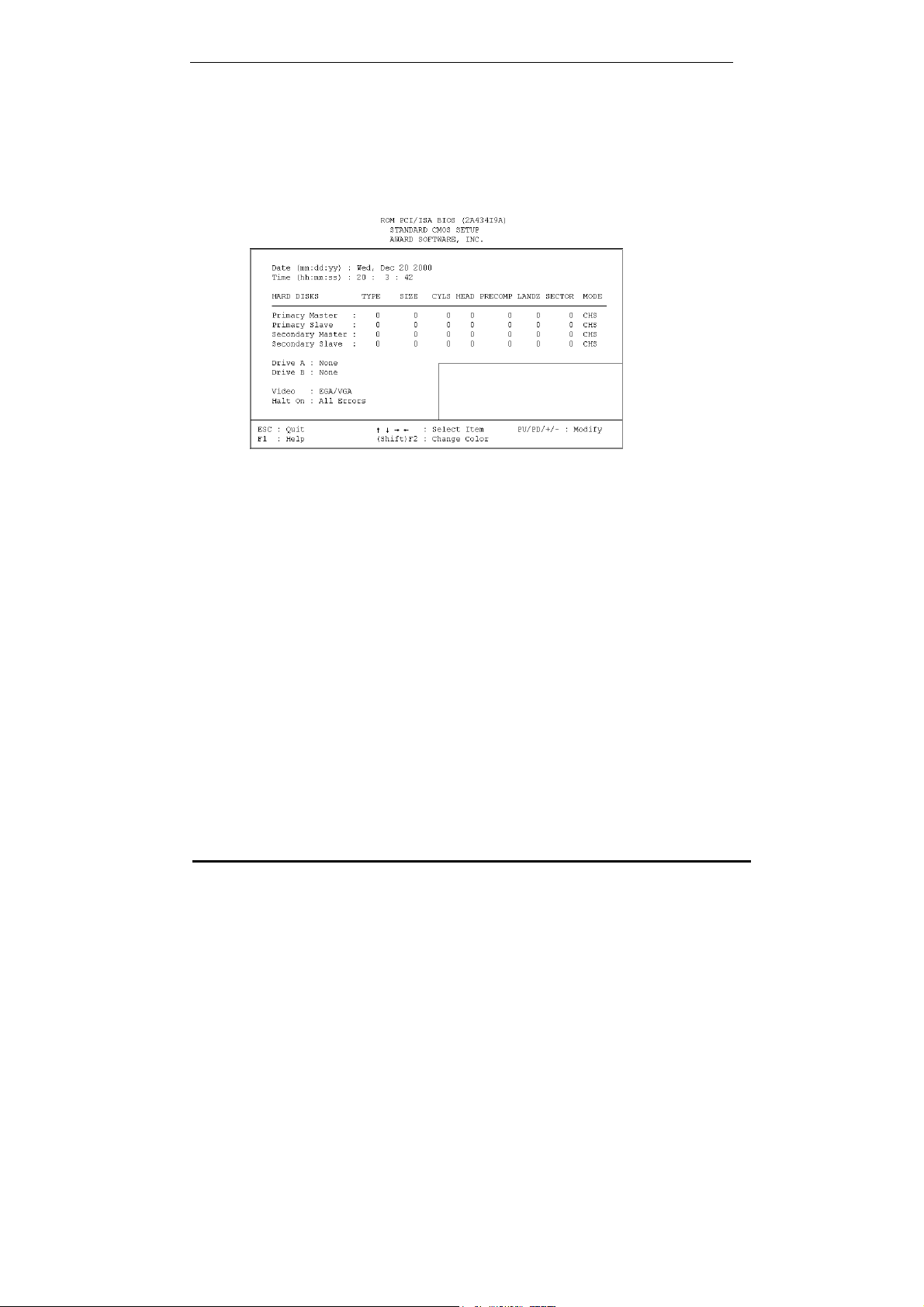
4.2 Standard CMOS Setup
The Standard CMOS Setup is used for basic hardware system
configuration. The main function is for Date/Time setting and
Floppy/Hard Disk Drive setting. Please refer the following screen for
this setup.
To set the Date, for example, press either the arrow or
<Enter> button on your keyboard to select one of the fields
(Month, Date or Year) then press either <PgUp> or <PgDn> to
increase or decrease the value of that field. Follow the same
steps for Time setting.
For IDE hard disk drive setup, please check the following
possible setup procedure:
1. Use the Auto setting for detection during boot-up.
2. Use the IDE HDD AUTO DETECTION in the main menu; the
computer will automatically detect the HDD specifications.
3. Manually enter the specifications by yourself from
the ”User“ option.
29
Page 32

Note:
If you need more information on any particular field, just highlight it
then press <F1> button. A pop-up window will come out to give you
more information on that field.
4.3 BIOS Features Setup
This BIOS Features Setup is designed for the 'fine tuning' of
your system in order to improve its performance. In normal
operation, you don‘t have to change any default setting. The
default setting is pre-set for most reliable operation.
30
Page 33
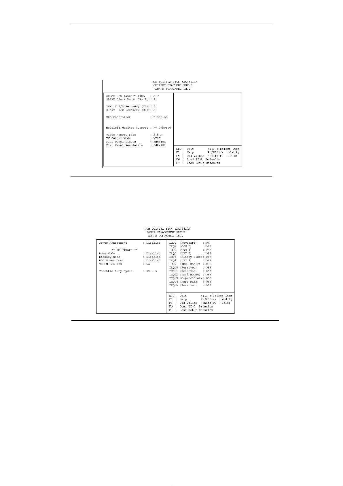
4.4 Chipset Features Setup
This setup function works mostly on board's chipset. This option
is used to change the chipset's configuration. Please proceed
carefully whilst changing any default setting, otherwise the
system will run unstable.
4.5 Power Management Setup
Power Management Setup helps user to handle the NOVA-4898
board‘s “green” function. Say for an example, this particular
feature can shut down the video display and hard disk to save
energy. The power management setup screen is shown below:
31
Page 34

4.6 PNP / PCI CONFIGURATION
This menu is used to assign certain IRQ to your PNP/PCI devices
manually.
PNP OS Installed: if you install Plug and Play operating
system (OS), the OS will reassign the interrupt if you select Yes
in this field. If you install a non-Plug and Play OS or if you want
to prevent reassigning of interrupt settings, select No in this
field.
Resources Controlled By: select Auto if you want the
computer to assign the IRQs automatically and vice versa.
Reset Configuration Data: Enabling this field means you
allow the configuration data to be reset.
IRQ-xx assigned to: these fields show whether a PCI/ISA
uses certain IRQ.
32
Page 35

r
4.7 LOAD BIOS DEFAULTS
If you select 'Y' to this field, the BIOS Defaults will be loaded
except Standard CMOS SETUP. The default settings are not
optimal and turning all high performance into disabled condition.
Select 'N' to abort.
Suggestion:
For the first time or for our primary user, we suggest you to use
LOAD SETUP DEFAULTS because it is the safest mode for you
system.
33
Page 36

4.8 LOAD SETUP DEFAULTS
If you select 'Y' to this field, the Setup Defaults will be loaded
except Standard CMOS SETUP. The default settings are optimal
configuration settings for your system.
4.9 INTEGRATED PERIPHERALS
34
Page 37

This option is used to assign Onboard I/O, IRQ, and DMA etc. If
you don't know how to configure them, just press <F7> to load
Setup Defaults.
The flat panels will then be applied with two modes: 640x480 or
800x600, for which it needs to set up from BIOS for proper flat
panel resolution.
Digital I/O Base Address -- 240H, 260H, 280H,
Disabled
To select the I/O address for digital I/O function.
Build in CPU Audio -- Enabled, Disabled
To disable/enable the audio function.
Audio I/O Base Address -- 220H, 240H, 260H, 280H
To select the I/O address for audio function.
MPU-401 I/O Base Address -- 300H, 330H, Disabled
To select the I/O address for MPU-401 (midi interface).
Audio IRQ Select -- 5, 7, 10, Disabled
To select the interrupt for audio function.
Audio Low DMA Select -- DMA0, DMA1, DMA3,
Disabled
To select the high DMA channel.
Audio High DMA Select -- DMA5, DMA6, DMA7,
Disabled
To select the high DMA channel.
Multiple Monitor Support -- No Onboard, PCI first, M/B
first
To select the primary VGA for multiple monitor support in
WINDOWS.
Video Memory Size -- 1.5M, 2.5M, 4.0M
To select the size of video memory. It makes use of system
memory for display.
TV-OUT Mode – NTSC, PAL
To select the TV-OUT mode.
35
Page 38

4.10 PASSWORD SETTING
Password SETTING sets a password that is used to protect
your system and Setup Utility. Once you setup the password,
the system will always ask you to key-in password every time
you enter the BIOS SETUP. If you enter the BIOS SETUP with
Password, you can choose from every setup/option on the
main menu. To disable the password, enter the BIOS SETUP
room with Password and then just press the <Enter> key
instead of entering a new password when the message 'Enter
Password' is prompted on your screen.
Note: if you forget the password, do the Clear/Reset
CMOS procedure (see Section 2.5 Clear CMOS Setup)
4.11 IDE HDD AUTODETECTION
This option detects the parameters of an IDE hard disk drive
(HDD sector, cylinder, head, etc) automatically and will put the
parameters into the Standard CMOS Setup screen. Up to 2 IDE
drives can be detected and the parameters will be listed in the
box. Press <Y> if you accept these parameters. Press <N> to
skip the next IDE drives.
Note: If your IDE HDD was formatted in previous version
of an older system, incorrect parameters may be
detected. In this case, you need to enter the correct
parameters manually or low-level format the disk
36
Page 39

4.12 SAVE AND EXIT SETUP
Select this option when you finish setting all the parameters and
want to save them into the CMOS. Simply press <Enter> key and all
the configuration changes will be saved.
37
Page 40

4.13 Quit Without Saving
Select this option if you want to exit the Setup without saving the
changes that you made. Just simply press <Enter> key and you will exit
the BIOS SETUP without saving the changes.
38
Page 41

5. SVGA Setup
5.1 Introduction
The NOVA-4898 is equipped with on-board LCD/VGA interface.
The its specifications and features described below:
5.1.1 Chipset
The NOVA-4898 uses a Cyrix CX5530 chipset as its SVGA
controller. It is compatible with many common 18-bit LCD
displays and traditional analog CRT monitors. The VGA BIOS
supports LCD. In addition, it also accepts interlaced and
non-interlaced analog monitors (color and monochrome VGA)
with high-resolution quality while maintaining complete IBM
VGA compatibility. But digital monitors (i.e. MDA, CGA, and
EGA) may be NOT supported. Multiple frequency (multisync)
monitors will be operated as if they were analog monitors.
5.1.2 Display memory
Having 1.5 ~ 4 MB UMA memory, the VGA controller can
make CRT displays or color panel displays perform resolutions
up to 1024 x 768 at 64 K colors. The display memory can be
modified up to 4 MB in BIOS for true-color resolution of 1024
x 768.
39
Page 42

5.1.3 Display drivers
1. Win95, 98 drivers (VGA & Audio) in
\VGA\MediaGX\National Geode Win9x Drivers 1.3
2. WinNT4.0 drivers in
\VGA\MediaGX\Nt40Vga\
5.2 Further Information
For more detailed information about the PCI/SVGA installation in
your NOVA-4898, including driver updates, troubleshooting
instructions, please refer to the website shown below where we
provide additional resources that you may need. If you could not
find the information you need, please contact with your local
contributor or ICP support team at:
ICP web site: www.ieiworld.com.tw
40
Page 43

6. Audio
6.1 Introduction
With on-board audio interface, NOVA-4898 can perform
high-quality stereo sound and FM music synthesis (ESFM) by using
the CX5530 audio controller. The audio interface has the following
functions namely recording, compressing, and playing back voice,
sound, and music with a built-in mixer control. In addition, the on
board audio interface supports the Plug and Play (PnP) standard and
provides PnP configuration for audio, FM, and MPU-104 logical
devices. It is compatible with AC97 version 2.0, voice, and music
functions. The ESFM synthesizer is registered compatible with the
OPL3 and has extended capabilities.
6.1.1 Audio drivers
1. Installing software driver in Windows NT
The driver was provided from the CD utility.
WinNT4.0 Audio drivers in
\Audio\MediaGX
2. Installing software driver in Win95/98
The software drivers was supported from Windows 95/98,
please set up from...
Win98\drivers\audio\cyrix\mgxsb16.inf
41
Page 44

7. PCI Bus Ethernet Interface
7.1 Introduction
The NOVA-4898 provides a high performance 32-bit Ethernet
chipset, which is completely compliant with IEEE 802.3 100 Mbps
CSMA/CD standards. It is both 100Base-T and 10Base-T compatible
so it is suitable for major network operating systems.
The Ethernet port supplies a standard RJ-45 connector on board.
In order to utilize the network boot feature, please add in the boot
ROM image files for the appropriate network operating system.
42
Page 45
Appendix A. Watchdog Timer
The Watchdog Timer is a device to ensure that standalone
systems can always recover from catastrophic conditions that cause
the CPU to crash. This condition may have occurred by external EMI
or a software bug. When the CPU stops working normally, hardware
on the board will perform hardware reset (cold boot) to bring the
system back to a known state.
Three I/O ports control the Watchdog Timer.
443 Write Set Watchdog Time period
443
(hex)
043/843
(hex)
Prior to enable the Watchdog Timer, user has to define Timer first.
The output data is the value of time interval. The range of value is
from 01(hex) to FF (hex) and 1 sec to 255 sec for time interval.
Read
Read Disable the Watchdog Timer.
Enable the refresh the Watch-Dog
Timer.
Data Time Interval
01 1 sec
02 2 sec
03 3 sec
04 4 sec
.
.
.
FF 255 sec
This action will enable and activate the countdown timer, which
will eventually time out, and reset the CPU to ensure that this reset
condition does not occur. The Watchdog Timer must be periodically
43
.
.
.
Page 46

refreshed by reading the same I/O port 043/843H and 443H. This
must be done within the time out period defined by software setting,
please refer to the example program.
A tolerance of at least 5% must be maintained to avoid unknown
routines within the operating system (DOS), such as disk I/O that
can be very time consuming. Therefore if the time out period has
been set to 10 seconds, the I/O port 443H must be read within 7
seconds.
Note:
When exiting a program it is necessary to disable the Watchdog
Timer, otherwise the system will reset.
Example assembly program
:
TIMER_PORT = 443H
TIMER_START = 443H
TIMER_STOP = 843H
;;INITIAL TIME PERIOD COUNTER
MOV DX, TIME_PORT
MOV AL, 8: ;;8 SECONDS
OUT DX,AL
;;ADD YOUR APPLICATION HERE
MOV DX, TIMER_START
IN AL, DX. ;;START COUNTER
44
Page 47

;;ADD YOUR APPLICATION HERE
W_LOOP:
MOV DX, TIMER_STOP
IN AL, DX
MOV DX, TIMER_START
IN AL, DX. ;;RESTART COUNTER
;;ADD YOUR APPLICATION HERE
CMP EXIT_AP, 0
JNE W_LOOP
MOV DX, TIMER_STOP
IN AL, DX
;;EXIT AP
45
Page 48

Appendix B. I/O Address Map
B.1 System I/O Address Map
I/O Address
Map
000-01F DMA Controller #1
020-021 Interrupt Controller # 1, Master
022-023 Chipset address
040-05F System Timer
060-06F
070-07F Real time Clock, NMI Controller
080-0BF DMA Page Register
0A0-0BF Interrupt Controller # 2
0C0-0DF DMA Controller # 2
0F0-0FF Math Coprocessor
170-1FF VIR BUS Master PCI IDE Controller
220-22F Audio 16bit sound
2E8-2EF Serial Port 4
2F8-2FF Serial Port 2
378-37F Parallel Printer Port 1
3B0-3DF Cyrix Graphic Adapter
3E8-3EF Serial Port 3
3F0-3F7 Floppy Disk Controller
3F8-3FF Serial Port 1
443 Watch dog timer enable
043/843 Watch dog timer disable
PNP audio I/O map range from 220~250H (16 bytes)
MPU-401 select from 300~330H (2 bytes)
Standard 101/102 keyboard
Controller
Description
46
Page 49

B.2 DMA Channel Assignments
Channel
0
1
2
3
4
5
6
7
Available
Audio*
Floppy disk (8-bit transfer)
Parallel**
Cascade for DMA controller
1
Audio*
Available
Available
* Audio DMA defaults setting: DMA 1.5
Audio High DMA select: DMA 1.3
Audio Low DMA select: DMA 5.6.7
** parallel port DMA default setting: DMA 3
parallel port DMA select: DMA 1.3
Function
B.3 Interrupt assignments
Interrupt
#
NMI Parity error detected
IRQ 0 System timer
IRQ 1 Keyboard
IRQ 2
Interrupt from controller 2
(cascade)
IRQ 8 Real-time clock
IRQ 9 LAN 82559
IRQ 10 Serial communication port 4
IRQ 11 Serial communication port 3
IRQ 12 PS/2 mouse
IRQ 13 Numeric data processor
IRQ 14 CX5530 Primary IDE controller
IRQ 15 CX5530 Second IDE controller
IRQ 3 Serial communication port 2
IRQ 4 Serial communication port 1
IRQ 5 Audio*
IRQ 6 Diskette controller (FDC)
IRQ 7 Parallel port 1 (print port)
Interrupt source
47
Page 50

* Audio default setting: IRQ5
Ethernet IRQ is automatic set by the system
B.4 1st MB memory map
Address Description
F000h-FFFFh System ROM
D800h-EFFFh Unused
C800h-D7FFh Ethernet ROM*
C000h-C7FFh Expansion ROM*
B800h-BFFFh CGA/EGA/VGA text
B000h-B7FFh Unused
A000h-AFFFh EGA/VGA graphics
0000h-9FFFh Base memory
D000-D400H Available
* Default setting
** If Ethernet boot ROM is enabled.
48
 Loading...