

Page 1

FIR-ULV600-DVR User Manual Page: 1/56
FIR-ULV600-DVR
User Manual
Version 1.0
POS+DVR
December 2005
Page 2

FIR-ULV600-DVR User Manual Page: 2/56
Copyright Notice
The information in this document is subject to change without prior notice in order to
improve reliability, design and function and does not represent a commitment on the
part of the manufacturer .
In no event will the manufacturer be liable for direct, indirect, special, incidental, or
consequential damages arising out of the use or inability to use the product or
documentation, even if advised of the possibility of such damages.
This document contains proprietary information protected by copyright. All rights are
reserved. No part of this manual may be reproduced by any mechanical, electronic, or
other means in any form without prior written permission of the manufacturer.
Trademarks
FIR-ULV600-DVR is registered trademarks of ICP Electronics Inc.; IBM PC is a
registered trademark of International Business Machines Corporation. INTEL is a
registered trademark of INTEL Corporation. AMI is registered trademarks of
American Megatrends Inc. Other product names mentioned herein are used for
identification purposes only and may be trademarks and/or registered trademarks of
their respective companies.
Support
Any questions regarding the content of this manual or related issues can be e-mailed
to us directly at: service@firich.com.tw
Page 3

FIR-ULV600-DVR User Manual Page: 3/56
Table of Contents
Chapter1 Introduction...............................................................................................5
1.1 Specification ...............................................................................................5
1.2 Package Contents........................................................................................7
Chapter2 Installation.................................................................................................8
2.1 Block Diagram & Board Layout.................................................................8
2.1.1 Block Diagram.................................................................................8
2.1.2 Board Layout ...................................................................................9
2.1.3 Board Dimension ...........................................................................10
2.2 Unpacking Precautions .............................................................................10
2.3 System Memory DRAM...........................................................................11
2.4 Clear CMOS Setup ...................................................................................11
2.5 TFT LCD Setting......................................................................................11
2.6 COM4 Voltage Selection ..........................................................................12
2.7 COM4 Mode Selection.............................................................................12
2.8 COM2 RI Function Setting.......................................................................12
2.9 COM1 RI Function Setting.......................................................................13
2.10 Keyboard Data & Clock by pass.............................................................13
2.11 COM5 & 6 RI (CN11 pin8 & 18) Function Setting................................13
Chapter3 Connection ..............................................................................................14
3.1 Compact Flash Storage Card Socket (CF1)..............................................14
3.2 Serial Port Connector (COM1, COM2, COM4, COM5 & COM6)..........15
3.3 Parallel Port Connector (LTP1).................................................................16
3.4 Primary IDE Connector (IDE1)................................................................17
3.5 VGA Connector (VGA1 & VGA2) ..........................................................18
3.6 CPU & system Fan Connector (J4 & J5)..................................................19
3.7 USB Connector (USB1 & USB2).............................................................19
3.8 LVDS Connector (LVDS1 & LVDS2)......................................................19
3.9 Box Header Connector (CN7) ..................................................................20
3.10 Keyboard/Mouse Connector (KB_MS1 & CN10) .................................21
3.11 Power Button (PS_ON1).........................................................................21
3.12 Power LED (LED1)................................................................................22
3.13 Power SW/LED Connector (CN4)..........................................................22
3.14 Digital I/O with RJ-11 Connector (CN2)................................................22
3.15 Power Connector (CN5 & CN8).............................................................23
3.16 LCD Back Light Connector (CN6 & CN9)............................................23
Page 4

FIR-ULV600-DVR User Manual Page: 4/56
3.17 Audio Connector.....................................................................................24
3.17.1 Speaker Out Phone Jack Connector (J6)......................................24
3.17.2 MIC In Phone Jack Connector (J7)..............................................24
3.17.3 Speaker Out Pin Header Connector (CN3)..................................24
Chapter4 BIOS Setup..............................................................................................25
4.1 Setup Menu...............................................................................................25
4.2 Setup Submenu: Main...............................................................................26
4.3 Setup Submenu: Advanced.......................................................................27
4.3.1 CPU Configuration ........................................................................28
4.3.2 IDE Configuration (Compatible Mode).........................................29
4.3.2.1 Primary IDE Master (if attached Hard Disk)......................30
4.3.3 Super IO Configuration..................................................................32
4.3.4 Hardware Health Configuration (Manual Mode) ..........................35
4.3.4.1 Hardware Health Configuration (Thermal Cruise Mode)...36
4.3.4.2 Hardware Health Configuration (Speed Cruise Mode) ......36
4.3.5 ACPI Configuration.......................................................................38
4.3.6 USB Configuration ........................................................................39
4.4 Setup submenu: Boot................................................................................40
4.4.1 Boot Settings Configuration ..........................................................41
4.4.2 Boot Device Priority......................................................................43
4.4.3 Hard Disk Drives ...........................................................................44
4.4.4 Removable Devices .......................................................................44
4.4.5 CD / DVD Drives...........................................................................45
4.5 Setup submenu: Security...........................................................................46
4.6 Setup submenu: Chipset............................................................................47
4.6.1 North Bridge Chipset Configuration..............................................48
4.6.2 South Bridge Chipset Configuration..............................................50
4.7 Setup submenu: Power..............................................................................51
4.8 Setup submenu: Exit.................................................................................52
Appendix A Address Mapping................................................................................54
A.1 I/O Address Map......................................................................................54
A.2 1st MB Memory Address Map.................................................................54
A.3 IRQ Mapping Chart .................................................................................55
A.4 DMA Channel Assignment......................................................................55
Appendix B Digital I/O...........................................................................................56
Page 5

FIR-ULV600-DVR User Manual Page: 5/56
Chapter1 Introduction
1.1 Specification
1. Form Factor
Form
Dimension: W 188 x D 122 mm
2. Processor Compatibility
Processor
CPU Type: Intel Celeron-M Processors
Max. Speed: Celeron-M 600MHz
FSB: 400 MHz
Package: Micro-FCBGA
L2 Cache: 0KB
CPU Process: 90nm
3. Main Chipset
North Bridge
Controller Hub: i82852GM GMCH
FSB: 400 MHz
VGA:
Dual independent pipe support: Concurrent, Simultaneous
◆ VGA port
◆ LVDS panel support
Memory: DDR 200/266 MHz up to 1GB
Package: 732-pin Micro-FCBGA (37.5 x 37.5 mm)
Hub Interface (HI): 66 MHz (266-MB/s)
South Bridge
Controller Hub: i82801DB ICH4
PCI Compliant: PCI 2.2
Package: 421-pin BGA (31x31 mm)
PCI Bus: Supports up to six master devices on PCI
Other Feature:
◆ 6 USB 2.0 ports, 480MB/s
◆ IDE up to ATA 100 mode
◆ AC'97 2.3 CODEC support
Page 6

FIR-ULV600-DVR User Manual Page: 6/56
◆ Power Management
◆ LPC interface to SIO and Flash BIOS
◆ SMBus 2.0
Firmware Hub: 4Mb Flash
4. Additional Chipset
LAN
Chipset: Realtek RTL8100BL
IEEE Compliant: IEEE 802.3u 100Base-T and IEEE 802.3x Full Duplex Flow
Control
Audio
Codec: AC'97 2.3 CODEC ALC202A
Rear panel output: Line-out, MIC-in
Hardware Monitor
Chipset: LPC I/O W83627EHF for onboard alarm
Super I/O
Chipset: Winbond 83627EHF
Fan: CPU Fan / System Fan
Monitor Voltage: TBD
Serial I/O
Chipset: FINTEK F81216D
COM 3, 4, 5, 6
Power Management
ACPI Support: ACPI 1.0b and 2.0
APM Support: APM Rev 1.2 compliant power management
Others:
◆ SMRAM space remapping to A0000h (128-kB)
◆ Support extended SMRAM space above 256-MB, additional 1-MB TSEG
from top of memory, cacheable (cache ability controlled by CPU)
◆ Support Suspend to System Memory, Suspend to Disk and Soft Off
◆ Enhanced Intel Speed Step technology support
◆ Optimized Clock Gating for 3D and Display Engines
◆ On-Die Thermal Sensor
Wakeup on LAN: TBD
Bootup Device
IDE device: Yes
Compact Flash: Yes
USB device: Yes
Page 7

FIR-ULV600-DVR User Manual Page: 7/56
ACPI 2.0
1.2 Package Contents
Before any installation, please check if the following materials are included in the
package:
z One FIR-ULV600-DVR all-in-one single board computer
z One compact disk for utility and drivers
If any of these items are missing or damaged, contact your distributor or sales
representative immediately.
Page 8
Chapter2 Installation
This chapter gives instructions about how to set up the FIR-ULV600-DVR hardware,
including directions of setting jumpers and connecting peripherals, switches and
indicators. Before installation, please pay attention to the unpacking precautions on
the following page for safety.
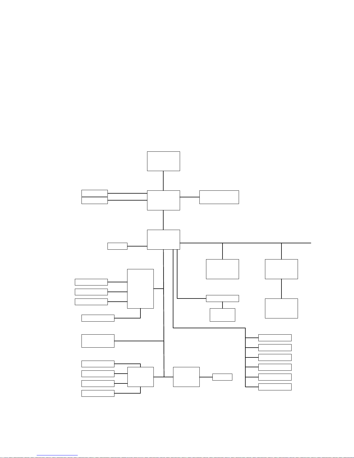
2.1 Block Diagram & Board Layout
2.1.1 Block Diagram
Intel
Celeron M
Intel
852GM
Intel
ICH4
PC-104 PLUS
LAN0
RTL 8100BL
Transformer
LAN
RJ45
DDR-SODIMM 0
200 / 266 MHz
DAC
LVDS
CRT PORT
LCD CONN
HDD
SUP I/O
W83627HF
LPT PORT
COM2 PORT
COM1 PORT
FAN CONN
BIOS
28F040T
LPC I/O
F81216D
LPC I/O
ITE8706
DIO
COM3 PORT
COM4 PORT
COM5 PORT
COM6 PORT
LPC
AC97 CODEC
AUDIO
CONN
AC97
USB PORT 0
USB PORT 1
USB PORT 2
USB PORT 3
USB PORT 4
USB PORT 5
USB 2.0
PCI BUS, 3.3V
RS232
RS232
RS232
RS232
FIR-ULV600-DVR User Manual Page: 8/56
Page 9
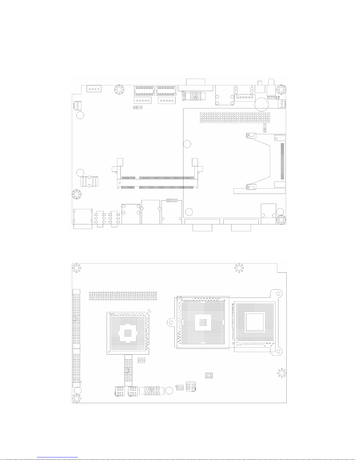
2.1.2 Board Layout
LVDS2
LVDS1
JP10 VGA2
VGA1
CN6
CN9
USB1
KB/MS
CN10
Button
LED
CN4
J5
JP2
CN5
J4
CN8
Power
J7 J6
MIC SPK
USB2 COM4
COM2 COM1
CN2
DIO
CF
JP7
Power
DDR DIMM Socket
LAN
J3
CN1
IDE1
LPT1
COM5
COM6
JP6
JP5
CN7
JP8
JP9
COM3+USB
JP11
CN3
CN11
+
FIR-ULV600-DVR User Manual Page: 9/56
Page 10
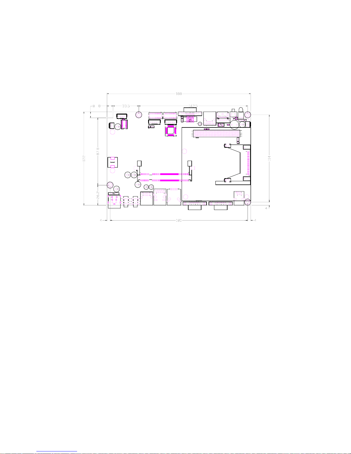
2.1.3 Board Dimension
z FIR-ULV-600’s Dimensions (Unit: mm)
2.2 Unpacking Precautions
Some components of FIR-ULV600-DVR SBC are very sensitive to static electric
charges and can be damaged by a sudden rush of power. To protect it from unintended
damage, be sure to note these precautions:
1. Ground yourself to remove any static charge before touching the
FIR-ULV600-DVR SBC. You can do it by using a grounded wrist strap at all
times or by frequently touching any conducting materials that is connected to the
ground.
2. Handle FIR-ULV600-DVR SBC by its edges. Don’t touch IC chips, leads or
circuitry if not necessary.
3. Do not plug any connector or jumper while the power is on.
FIR-ULV600-DVR User Manual Page: 10/56
Page 11
FIR-ULV600-DVR User Manual Page: 11/56
2.3 System Memory DRAM
There are one 200-pin DDR SO-DIMM sockets to accept 2.5V non-buffered SDRAM.
The max Memory size is 1GB.
2.4 Clear CMOS Setup
To clear the CMOS Setup (for example, if you have forgotten the password, you
should clear the CMOS and then re-set the password), you have to close the JP2 (2-3)
for about 3 seconds, and then open it. This will put the system back to normal
operation mode.
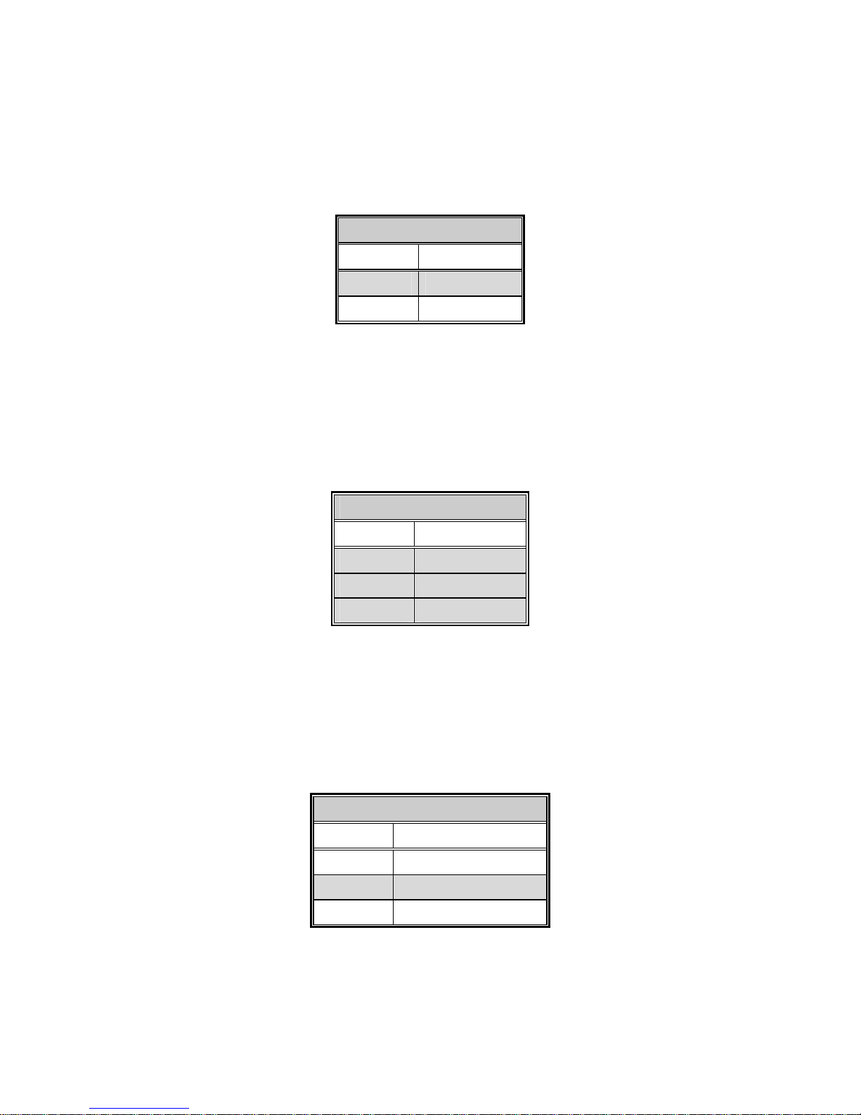
z JP2: Clear CMOS Setup
JP2
PIN STATE DESCRIPTION
Short 1-2
(default)*
Keep CMOS Setup
(Normal Operation)
Short 2-3 Clear CMOS Setup
*Note: All shaded rows in the tables of this manual are the default settings.
2.5 TFT LCD Setting
z JP7/JP10: TFT LCD Voltage (5V / 3V) Setting
JP7 for LVDS1, JP10 for LVDS2
JP7 & JP10
PIN STATE DESCRIPTION
Short 1–2 3V TFT LCD
Short 2–3 5V TFT LCD
Page 12
FIR-ULV600-DVR User Manual Page: 12/56
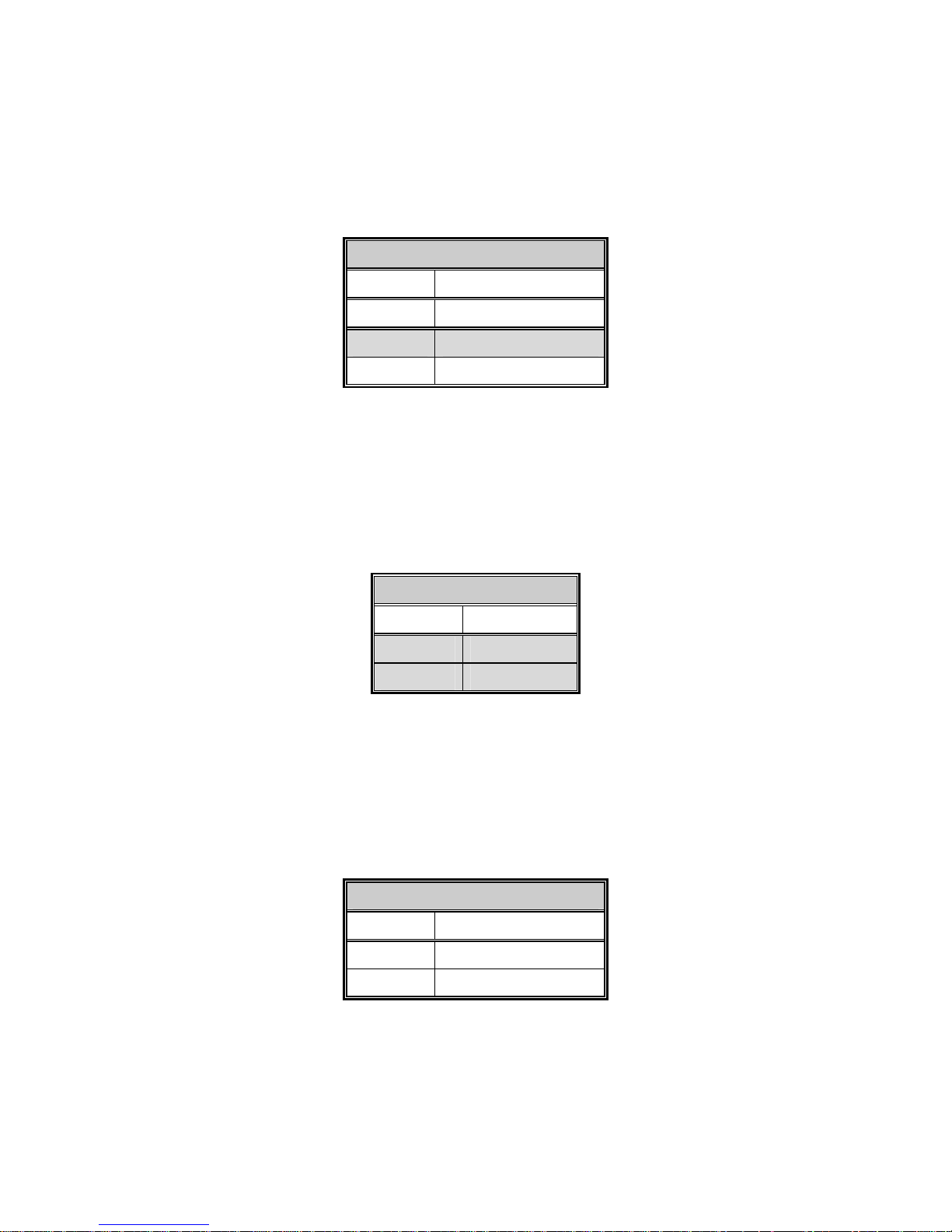
2.6 COM4 Voltage Selection
z JP8: COM4 Voltage Selection
JP8
PIN STATE DESCRIPTION
Short 1-2 +12V
Short 2-3 +5V
2.7 COM4 Mode Selection
z JP9: COM4 Mode Selection
JP9
PIN STATE DESCRIPTION
Short 1-2 CTS RTS short
Short 3-5 +12V/+5V output
Short 4-6 Ground output
2.8 COM2 RI Function Setting
z JP5: COM2 RI Function Setting
JP5
PIN STATE DESCRIPTION
Short 1-2 RI is +5 Voltage output
Short 3-4 RI function
Short 5-6 RI is +12 Voltage output
Page 13
FIR-ULV600-DVR User Manual Page: 13/56
2.9 COM1 RI Function Setting
z JP6: COM1 RI Function Setting
JP6
PIN STATE DESCRIPTION
Short 1-2 RI is +5 Voltage output
Short 3-4 RI function
Short 5-6 RI is +12 Voltage output
2.10 Keyboard Data & Clock by pass
z CN10: Keyboard Data & Clock by pass
CN10
PIN STATE DESCRIPTION
Short 2-3 Clo ck by pass
Short 4-5 Data by pass
2.11 COM5 & 6 RI (CN11 pin8 & 18) Function Setting
z JP11: COM5 & 6 RI Function Setting
JP11
PIN STATE DESCRIPTION
Short 1-2 RI is +12 Voltage output
Short 3-4 RI is +5 Voltage output
Page 14

FIR-ULV600-DVR User Manual Page: 14/56
Chapter3 Connection
This chapter describes how to connect peripherals, switches and indicators to the
FIR-ULV600-DVR board.
z Table of Connectors
LEBAL FUNCTION
L V DS1 & 2 L V DS LCD Panel connectors
VGA1 & 2 VGA connectors
LAN LAN RJ45 connector
USB1 & 2 USB dual port connectors
COM1, 2, 4, 5 & 6 Serial port connectors
KB_MS1 Keyboard & Mouse connector
J4 & 5 Fan connectors
J6 Speaker out phone jack connector
J7 MIC in phone jack connector
CN3 Speaker out pin header connector
LPT1 Parallel port connector
IDE1 Ultra ATA100 Primary IDE connectors
CF1 Compact Flash Storage Card Type II connecto
r
PS_ON1 Power on Switch
LED1 Power LED
CN1 PC/104 Plus connector
CN2 Digital I/O with RJ-11 connector
CN4 Power SW/LED connector
CN5 Power output connector
CN6 & 9 LCD back light connectors
CN7 Multi-function connector
CN8 +12V DC power connector
CN10 Internal Keyboard connector
CN1 1 Serial port connectors
3.1 Compact Flash Storage Card Socket (CF1)
Page 15

z Compact Flash Storage Card Socket
FIR-ULV600-DVR User Manual Page: 15/56
CF1
PIN NO. DESCRIPTION PIN NO. DESCRIPTION
1 GROUND 26 PULL DOWN
2 D3 27 D11
3 D4 28 D12
4 D5 29 D13
5 D6 30 D14
6 D7 31 D15
7 CS1# 32 CS3#
8 N/C 33 N/C
9 GROUND 34 IOR#
10 N/C 35 IOW#
11 N/C 36 VCC
12 N/C 37 IRQ15
13 VCC 38 VCC
14 N/C 39 MASTER/SLAVE
15 N/C 40 N/C
16 N/C 41 RESET#
17 N/C 42 IORDY
18 A2 43 DREQ
19 A1 44 DACK#
20 A0 45 ACTIVE#
21 D0 46 PDIAG#
22 D1 47 D8
23 D2 48 D9
24 N/C 49 D10
25 PULL DOWN 50 GROUND
3.2 Serial Port Connector (COM1, COM2, COM4,
COM5 & COM6)
z COM1 & COM2: D-SUB Serial Port Connectors
Page 16
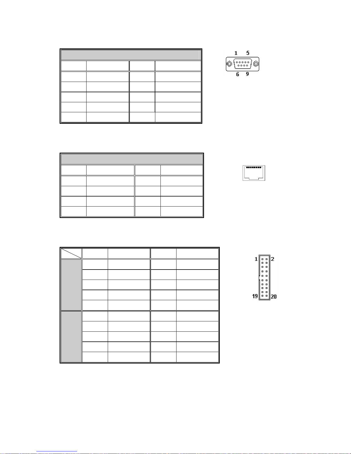
FIR-ULV600-DVR User Manual Page: 16/56
COM1 & COM2
PIN NO.
DESCRIPTION PIN NO. DESCRIPTION
1 (DCD) 6 (DSR)
2 (RXD) 7
(RTS)
3 (TXD) 8 (CTS)
4 (DTR)
9
(RI or 5V or 12V)
5 GROUND
10 N/C
z COM4: RJ45 Serial Port Connector
COM4
PIN NO.
DRSCRIPTION PIN NO. DESCRIPTION
1 +12/+5V 5 DTR
2 +12/+5V or CTS 6 DSR
3 GROUND 7
TXD
4 GROUND or RTS 8 RXD
z COM5 & COM6: Serial Port Connector
PIN NO.
DESCRIPTION PIN NO.
DESCRIPTION
1 (DCD) 2 (DSR)
3 (RXD) 4 (RTS)
5 (TXD) 6 (CTS)
7 (DTR) 8 +5V or +12V
COM5
9 GROUND 10 GROUND
11 (DCD) 12 (DSR)
13 (RXD) 14 (RTS)
15 (TXD) 16 (CTS)
17 (DTR) 18 +5V or +12V
COM6
19 GROUND 20 GROUND
3.3 Parallel Port Connector (LTP1)
Page 17
z LPT1: Parallel Port Connector
FIR-ULV600-DVR User Manual Page: 17/56
LTP1
IN NO.DESCRIPTION
IN NO..DESCRIPTION
1 STROBE# 14 AUTO FORM FEED #
2 DATA 0 15 ERROR#
3 DATA 1 16 INITIALIZE
4 DATA 2 17 PRINTER SELECT IN
#
5 DATA 3 18 GROUND
6 DATA 4 19 GROUND
7 DATA 5 20 GROUND
8 DATA 6 21 GROUND
9 DATA 7 22
GROUND
10 ACKNOWLEDGE 23
GROUND
11 BUSY 24
GROUND
12 PAPER EMPTY 25
GROUND
13 PRINTER SELEC
T
26
N/C
3.4 Primary IDE Connector (IDE1)
z IDE1: Primary IDE Connector
IDE1
PIN NO. DESCRIPTION PIN NO. DESCRIPTION
1 RESET# 2 GROUND
3 DATA 7 4 DATA 8
5 DATA 6 6 DATA 9
7 DATA 5 8 DATA 10
9 DATA 4 10 DATA 11
1 1 DATA 3 12 DATA 12
13 DATA 2 14 DAT A 13
15 DATA 1 16 DAT A 14
17 DATA 0 18 DAT A 15
19 GROUND 20 N/C
Page 18

21 DRQ 22 GROUND
23 IOW# 24 GROUND
25 IOR# 26 GROUND
27 CHRDY 28 REV. PULL LOW
29 DACK 30 GROUND-DEFAULT
31 INTERRUPT 32 N/C
33 SA1 34 PD66 SELECT
35 SA0 36 SA2
37 HDC CS0# 38 HDC CS1#
39 HDD ACTIVE# 40 GROUND
41 VCC 42 VCC
43 GROUND 44 N/C
3.5 VGA Connector (VGA1 & VGA2)
z VGA1: 15-pin Female Connector
VGA1
PIN NO.
DESCRIPTION PIN NO. DESCRIPTION
1 RED 2 GREEN
3 BLUE 4 NC
5 GROUND 6 GROUND
7 GROUND 8 GROUND
9 VCC / NC 10 GROUND
11 NC 12 DDC DAT
13 HSYNC 14 VSYNC
15 DDCCLK
z VGA2: 10-pin Box Header Connector
VGA2
PIN NO.
DESCRIPTION PIN NO.
DESCRIPTION
1
RED
6
DDCCLK
2
GREEN
7
DDCDAT
FIR-ULV600-DVR User Manual Page: 18/56
Page 19

3
BLUE
8
GROUND
4
HSYNC
8
GROUND
5
VSYNC
10
GROUND
3.6 CPU & system Fan Connector (J4 & J5)
z J4: CPU Fan Connector
z J5: system Fan Connector
FIR-ULV600-DVR User Manual Page: 19/56
J4 & J5
PIN NO. DESCRIPTION
1 Rotation Signal
2
+12V
3 Ground
3.7 USB Connector (USB1 & USB2)
z USB1 & USB2: 2 ports USB Connectors
USB1 & USB2
PIN NO.
DESCRIPTION PIN NO. DESCRIPTION
1 USB Power 5 USB Power
2 DATA4- 6 DATA5-
3 DATA4+ 7 DATA5+
4 GROUND 8 GROUND
3.8 LVDS Connector (LVDS1 & LVDS2)
z LVDS1 & LVDS2: LVDS Connectors
Page 20

LVDS1 & LVDS2
PIN NO. DESCRIPTION PIN NO. DESCRIPTION
1 GROUND 2 GROUND
3 CH1 DAT A3+ 4 CH1 DATA35 CH1 CLK+ 6 CH1 CLK7 CH1 DAT A2+ 8 CH1 DATA29 CH1 DATA1+ 10 CH1 DATA1-
1 1 CH1 DATA0+ 12 CH1 DATA013 GROUND 14 GROUND
15 CH2 DATA 3+ 4 CH2 DATA317 CH2 CLK+ 6 CH2 CLK19 CH2 DATA 2+ 8 CH2 DATA221 CH2 DATA 1+ 10 CH2 DATA123 CH2 DATA 0+ 12 CH2 DATA025 GROUND 26 GROUND
27 LCD power 28 LCD power
29 LCD power 30 LCD power
3.9 Box Header Connector (CN7)
z CN7: COM3 & USB Box Header Connector
CN7
PIN NO.
DESCRIPTION PIN NO. DESCRIPTION
1 VCC 2 VCC
3 USB1- 4
USB0-
5 USB1+ 6 USB0+
7 GND
8
GND
9 DTR
10
CTS
11 RTS
12
TXD
13 RXD
14
DSR
FIR-ULV600-DVR User Manual Page: 20/56
Page 21

3.10 Keyboard/Mouse Connector (KB_MS1 & CN10)
z KB_MS1: Mini DIN Keyboard/Mouse Connector
KB_MS1
PIN NO. DESCRIPTION
1 KEYBOARD DATA
2 MOUSE DATA
3 GROUND
4 +5V
5 KEYBOARD CLOCK
6 MOUSE CLOCK
z CN10: 6-pin Keyboard Connector
CN10
PIN NO. DESCRIPTION
1 +5V
2 KEYBOARD CLOCK
3 PC KB CLOCK
4 KEYBOARD DATA
5 PC KB DATA
6 GROUND
Note: Default short pin 2-3, 4-5
3.11 Power Button (PS_ON1)
z PS_ON1: Power Button
FIR-ULV600-DVR User Manual Page: 21/56
PS_ON1
PIN NO.
DESCRIPTION PIN NO. DESCRIPTION
1 GROUND 2 PS_ON
3 GROUND 4 GROUND
Page 22

3.12 Power LED (LED1)
z LED1: Power LED
LED1
PIN NO.
DESCRIPTION PIN NO. DESCRIPTION
1 +5V 2 GROUND
3 +5V Standby
3.13 Power SW/LED Connector (CN4)
z CN4: Power SW/ LED Connector
CN4
PIN NO.
DESCRIPTION
1 LED ON +
2 LED OFF +
3 GROUND
4 PS ON
3.14 Digital I/O with RJ-11 Connector (CN2)
z CN2: Digital I/O with RJ-11 Connector
CN2
PIN NO.
DESCRIPTION PIN NO. DESCRIPTION
1 GROUND 2 DGI/O OUT 0
3 DGI/O IN 0 4 +12V
5 DGI/O OUT 1 6 GROUND
FIR-ULV600-DVR User Manual Page: 22/56
Page 23

3.15 Power Connector (CN5 & CN8)
z CN5: Power 4P Connector
FIR-ULV600-DVR User Manual Page: 23/56
CN5
PIN NO. DESCRIPTION
1 +5V
2 GROUND
3 GROUND
4 +12V
z
CN8: 12V DC Power Connector
CN8
PIN NO.
DESCRIPTION PIN NO. DESCRIPTION
1 +12V 2 GROUND
3 +12V 4 GROUND
3.16 LCD Back Light Connector (CN6 & CN9)
z CN6 / CN9: LCD Back Light Connector
CN6 for LVDS1, CN9 for LVDS2
CN6 & CN9
PIN NO.
DESCRIPTION
1 +12V
2 +12V
3 GROUND
4 GROUND
5 LCD_BKLEN
Page 24

3.17 Audio Connector
3.17.1 Speaker Out Phone Jack Connector (J6)
z J6: Speaker Out Phone Jack Connector
J6
PIN NO. DESCRIPTION PIN NO. DESCRIPTION
1 NC 2 GROUND
3 Line Out (Left) 4 Speaker Out (Right)
3.17.2 MIC In Phone Jack Connector (J7)
z J7: MIC In Phone Jack Connector
J7
PIN NO. DESCRIPTION PIN NO. DESCRIPTION
1 NC 2 GROUND
3 MIC In 4 NC
3.17.3 Speaker Out Pin Header Connector (CN3)
z CN3: Speaker Out Pin Header Connector
CN3
PIN NO. DESCRIPTION PIN NO. DESCRIPTION
1 SPK Out (Left) 2 GROUND
3 SPK Out (Right) 4 GROUND
FIR-ULV600-DVR User Manual Page: 24/56
Page 25

FIR-ULV600-DVR User Manual Page: 25/56
Chapter4 BIOS Setup
4.1 Setup Menu
The BIOS (Basic Input and Output System) Setup utility is a menu driven utility that
enables you to make changes to the system configuration and tailor your system to
suit your individual work needs. BIOS is a ROM-based configuration utility that
displays the system’s configuration status and provides you with a tool to set system
parameters. These parameters are stored in non-volatile battery-backed-up CMOS
RAM that saves this information even when the power is turned off. When the system
is turned back on, the system is configured with the values found in CMOS.
Configure such items as:
Hard drives, diskette drives, and peripherals
Password protection from unauthorized use
Power Management Features
This Setup utility should be executed under the following conditions:
When changing the system configuration
When a configuration error is detected by the system and you are prompted to make
changes to the Setup utility
When redefining the communication ports to prevent any conflicts
When making changes to the Power Management configuration
When changing the password or making other changes to the security setup
BIOS Setup Options at Boot
The user will be able to initiate SETUP by pressing the respective key.
Press Delete to run Setup
Page 26

FIR-ULV600-DVR User Manual Page: 26/56
4.2 Setup Submenu: Main
BIOS Setup Utility
Main Advanced Boot Security Chipset Power Exit
AMIBIOS
Core Ver :08.00.11
Build Date :MM/DD/YY
BIOS Ver :B004MRXX
Processor
Type : Intel (R) Celeron(R) processor
Speed
: 600MHz
Count : 1
System Memory
Size : XXXXMB
System Time [XX:XX:XX]
Sy stem Date
[Date MM/DD/YYYY]
Here displays HELP
comment….
←→ Select Screen
↑↓ Select Item
+ - Change Option
Tab Select Field
F1 General Help
F10 Save and Exit
ESC Exit
V02.57 ©Copyright 1985-2002, American Megatrends Inc.
Page 27

FIR-ULV600-DVR User Manual Page: 27/56
4.3 Setup Submenu: Advanced
BIOS Setup Utility
Main Advanced Boot Security Chipset Power Exit
Advanced Settings
----------------------------------------------------------------------------------
WARNING: Setting wrong values in below sections
May cause system to malfunction.
►CPU Configuration
► IDE Configuration
► SuperIO Configuration
► Hardware Health Configuration
► ACPI Configuration
► USB Configuration
Here displays HELP
comment….
←→ Select Screen
↑↓ Select Item
+ - Change Option
Tab Select Field
F1 General Help
F10 Save and Exit
ESC Exit
V02.57 ©Copyright 1985-2002, American Megatrends, Inc.
Page 28

FIR-ULV600-DVR User Manual Page: 28/56
4.3.1 CPU Configuration
BIOS Setup Utility
Advanced
Configuration Advanced CPU Settings
Module Version : 12.00
----------------------------------------------------------------------------------
Manufacturer :Intel
Brand String :Intel (R) Celeron(R) processor
Frequency :600MHz
FSB Speed :400MHz
Cache L1 :32 KB
Cache L2 : 0 KB
CPU TM function [En/Disable]
Here displays HELP
comment….
←→ Select Screen
↑↓ Select Item
+ - Change Option
F1 General Help
F10 Save and Exit
ESC Exit
V02.57 ©Copyright 1985-2002, American Megatrends, Inc.
z Options summary
Disabled
CPU TM function
Enable Optimal Default, Failsafe Default
This item en/disables TM (thermal management) function of CPU
Page 29

FIR-ULV600-DVR User Manual Page: 29/56
4.3.2 IDE Configuration (Compatible Mode)
BIOS Setup Utility
Advanced
IDE Configuration
----------------------------------------------------------------------------------
Onboard PCI IDE Controller [Option]
► Primary IDE 0 [Hard Disk]
► Primary IDE 1 [Not Detected]
► Secondary IDE 0 [Not Detected]
► Secondary IDE 1 [Not Detected]
Here displays HELP
comment….
←→ Select Screen
↑↓ Select Item
+ - Change Option
F1 General Help
F10 Save and Exit
ESC Exit
V02.57 ©Copyright 1985-2002, American Megatrends, Inc.
z Options summary
Disabled
Onboard PCI IDE Controller
Primary Optimal Default, Failsafe Default
Select how PCI IDE Controller works.
Disabled: No device
Primary: Enables primary IDE controller.
Page 30

FIR-ULV600-DVR User Manual Page: 30/56
4.3.2.1 Primary IDE Master (if attached Hard Disk)
BIOS Setup Utility
Advanced
Primary IDE Master
___________________________________________________
Device : Hard Disk
Vendor : IBM-DTTA-351010
Size : 10.1GB
LBA Mode : Supported
Block Mode : 16Sectors
PIO Mode : 4
Async Mode : MultiWord DMA-2
Ultra DMA : Ultra DMA-2
S.M.A.R.T. : Supported
____________________________________________________
Type [Aut o]
LBA/Large Mode [Auto]
Block Mode [Auto]
PIO Mode [Auto]
DMA Mode [Auto]
S.M.A.R.T. [Auto]
32Bit Dat a Transfer [Disabled]
Here displays HELP
comment….
←→ Select Screen
↑↓ Select Item
+ - Change Option
F1 General Help
F9 Load Defaults
F10 Save and Exit
ESC Exit
V02.57 ©Copyright 1985-2002, American Megatrends, Inc.
z Options summary
Not Installed
Auto Optimal Default, Failsafe Default
CDROM
Type
ARMD
Select the type corresponding to the device present.
N
ot Installed: No device
Auto: Auto detected
CDROM: A TAPI CDROM
ARMD: ATAPI Removable Media Device
Disabled
LBA/Large Mode
Auto Optimal Default, Failsafe Default
Page 31

FIR-ULV600-DVR User Manual Page: 31/56
Disabled: Disables LBA Mode.
Auto: Enables LBA Mode if the device supports it and the device is not already formatted with LBA
Mode disabled.
Disabled
Block (Multi-Sector Transfer)
Auto Optimal Default, Failsafe Default
Disabled: The Data transfer from and to the device occurs one sector at a time.
Auto: The Data transfer from and to the device occurs multiple sectors at a time if the device supports it.
Auto Optimal Default, Failsafe Default
0
1
2
3
PIO Mode
4
Auto Optimal Default, Failsafe Default
SWDMA0
SWDMA1
SWDMA2
MWDMA0
MWDMA1
MWDMA2
UDMA0
UDMA1
UDMA3
DMA Mode
UDMA4
Select DMA Mode.
Auto: Auto detected
SWDMA n: Single Word DMA n
MWDMA n: Multiword DMA n
UDMA n: Ultra DM A n
Auto Optimal Default, Failsafe Default
Disabled
S.M.A.R.T.
Enabled
S.M.A.R.T. stands for “Self-Monitoring, Analysis and Reporting Technology”.
Disabled Failsafe Default
32Bit Data Transfer
Enabled Optimal Default
Page 32

4.3.3 Super IO Configuration
FIR-ULV600-DVR User Manual Page: 32/56
z Options summary
Disabled
3F8/IRQ4 Optimal Default, Failsafe Default
3E8/IRQ4
Serial Port1 Address (/IRQ)
2E8/IRQ3
This item selects Serial Port1 Base Addresses.
Disabled
2F8/IRQ3 Optimal Default, Failsafe Default
3E8/IRQ4
Serial Port2 Address (/IRQ)
2E8/IRQ3
This item selects Serial Port2 Base Addresses.
Normal Optimal Default, Failsafe Default
IrDA
BIOS Setup Utility
Advanced
Configuration NAT417 Super IO Chipset
___________________________________________________
Serial Port1 Address(/IRQ) [3F8/IRQ4]
Serial Port2 Address(/IRQ) [2F8/IRQ3]
Serial Port1 Mode [normal]
Parallel Port Address [378]
Parallel Port Mode [normal]
Parallel Port IRQ [IRQ7]
Digital I/O Function [280h]
Serial Port3 Address(/IRQ) [3E8]
Serial Port3 IRQ [10]
Serial Port4 Address(/IRQ) [2E8]
Serial Port4 IRQ [11]
Serial Port5 Address(/IRQ) [4F8]
Serial Port5 IRQ [5]
Serial Port6 Address(/IRQ) [4E8]
Serial Port6 IRQ [11]
Here displays HELP
comment….
←→ Select Screen
↑↓ Select Item
Enter Go to Sub Screen
F1 General Help
F10 Save and Exit
E SC Exit
V02.57 ©Copyright 1985-2002, American Megatrends, Inc.
Page 33

FIR-ULV600-DVR User Manual Page: 33/56
Ask IR
This Item selects mode for Serial Port1.
Disabled Failsafe Default
378 Optimal Default
278
Parallel Port Address
3BC
This item selects Parallel Port Base Addresses. Mode setting and IRQ setting below will not appear if
disabled
Normal
Bi-Directional
Optimal Default, Failsafe Default
EPP
ECP
Parallel port Mode
EPP+ECP
This Item selects mode for Parallel Port.
IRQ5
Parallel port IRQ
IRQ7 Optimal Default, Failsafe Default
This item selects IRQ for Parallel Port.
200h
220h
240h
260h
Digital I/O Function
280h Optimal Default, Failsafe Default
This item selects base address of SIO digital I/O function.
Disabled
3E8 Optimal Default, Failsafe Default
2E8
4F8
Serial Port3 Address
4E8
This item selects Serial Port3 Base Addresses.
5
10
Serial Port3 IRQ
11 Optimal Default, Failsafe Default
This item selects IRQ for Serial Port3.
Disabled
3E8
2E8 Optimal Default, Failsafe Default
Serial Port4 Address
4F8
Page 34

FIR-ULV600-DVR User Manual Page: 34/56
4E8
This item selects Serial Port4 Base Addresses.
5
10
Serial Port4 IRQ
11 Optimal Default, Failsafe Default
This item selects IRQ for Serial Port4.
Disabled
3E8
2E8
4F8 Optimal Default, Failsafe Default
Serial Port5 Address
4E8
This item selects Serial Port5 Base Addresses.
5 Optimal Default, Failsafe Default
10
Serial Port5 IRQ
11
This item selects IRQ for Serial Port5.
Disabled
3E8
2E8
4F8
Serial Port6 Address
4E8 Optimal Default, Failsafe Default
This item selects Serial Port6 Base Addresses.
5
10
Serial Port6 IRQ
11 Optimal Default, Failsafe Default
This item selects IRQ for Serial Port6.
Page 35

FIR-ULV600-DVR User Manual Page: 35/56
4.3.4 Hardware Health Configuration (Manual Mode)
BIOS Setup Utility
Advanced
Hardware Health Configuration
System Temperature #1 : XX°C/XX°F
CPU Temperature : XX°C/XX°F
System Temperature #2 : XX°C/XX°F
SYSFAN Speed XXXXRPM
CPUFAN0 Speed XXXXRPM
VCore : X.XX V
3Vcc : X.XX V
+12.0V : X.XX V
+1.50V : X.XX V
+1.20V : X.XX V
+5.00V : X.XX V
+2.50V : X.XX V
SYSFAN Mode Settig [Manual Mode ]
SYSFAN Control [value]
CPUFAN0 Mode Settig [Manuak Mode ]
CPUF AN0 Control [value]
Here displays HELP
comment….
←→ Select Screen
↑↓ Select Item
+ - Change Option
F1 General Help
F10 Save and Exit
ESC Exit
V02.57 ©Copyright 1985-2002, American Megatrends, Inc.
Page 36

FIR-ULV600-DVR User Manual Page: 36/56
4.3.4.1 Hardware Health Configuration (Thermal Cruise Mode)
BIOS Setup Utility
Advanced
Hardware Health Configuration
System Temperature #1 : XX°C/XX°F
‧
‧
‧
+2.50V : X.XX V
SYSFAN Mode Settig [Thermal Cruise mode ]
SYSFAN TartgetTemp Value [value]
SYSFAN Tolerance Value [value]
SYSFAN Startup Value [value]
SYSFAN Stop Value [value]
SYSFAN Stop Time Value [value]
CPUFAN0 Mode Settig [Manuak Mode ]
CPUF AN0 Control [value]
Here displays HELP
comment….
←→ Select Screen
↑↓ Select Item
+ - Change Option
F1 General Help
F10 Save and Exit
E SC Exit
V02.57 ©Copyright 1985-2002, American Megatrends, Inc.
4.3.4.2 Hardware Health Configuration (Speed Cruise Mode)
BIOS Setup Utility
Advanced
Hardware Health Configuration
System Temperature #1 : XX°C/XX°F
‧
‧
‧
+2.50V : X.XX V
SYSFAN Mode Settig [Speed Cruise Mode ]
SYSFAN TartgetSpeed Value [value]
SYSFAN Tolerance Value [value]
CPUFAN0 Mode Settig [Manuak Mode ]
CPUF AN0 Control [value]
Here displays HELP
comment….
←→ Select Screen
↑↓ Select Item
+ - Change Option
F1 General Help
F10 Save and Exit
E SC Exit
V02.57 ©Copyright 1985-2002, American Megatrends, Inc.
Page 37

FIR-ULV600-DVR User Manual Page: 37/56
z Options summary
Manual Mode Optimal Default, Failsafe Default
Thermal Cruise Mode
SYSFAN Mode Setting
CPUFAN0 Mode Setting
Speed Cruise Mode
These item selects FAN configuration mode:
Manual Mode: Controls FAN by manual.
Thermal Cruise Mode: Temperature targeting mode.
Speed Cruise Mode: FAN speed targeting mode.
z Manual Mode
F A N CO NTR OL
250 Optimal Default, Failsafe Default
This item controls DC voltage of FAN. Max =255
z Thermal Cruise Mode
SYSF AN TargetTemp value
055 Optimal Default, Failsafe Default
This item determines target temperature. Max =255
SYSF AN Tolerance value
03 Optimal Default, Failsafe Default
This item determines tolerance of target temperature. Max =15
SYSFAN StartUp value
096 Optimal Default, Failsafe Default
This item determines Fan start up value. Max =255
SYSFAN Stop value
064 Optimal Default, Failsafe Default
This item determines FAN stop value. Max =255
SYSF AN Stop Time value
060 Optimal Default, Failsafe Default
This item determines FAN stop time value. Max =255
z Speed Cruise Mode
SYSF AN TargetTemp value
055 Optimal Default, Failsafe Default
This item determines target FAN speed. Max =255
SYSF AN Tolerance value
03 Optimal Default, Failsafe Default
This item determines tolerance of target speed. Max =15
Page 38

FIR-ULV600-DVR User Manual Page: 38/56
4.3.5 ACPI Configuration
BIOS Setup Utility
Advanced
ACPI Settings
ACPI Aware O/S [Yes]
Here displays HELP
comment….
←→ Select Screen
↑↓ Select Item
+ - Change Option
F1 General Help
F9 Load Defaults
F10 Save and Exit
ESC Exit
V02.57 ©Copyright 1985-2002, American Megatrends, Inc.
z Options summary
No
ACPI A ware O/S
Yes Optimal Default, Failsafe Default
This item En/Disables ACPI to fit supportability of Operation System.
Page 39

FIR-ULV600-DVR User Manual Page: 39/56
4.3.6 USB Configuration
BIOS Setup Utility
Advanced
USB Configuration
USB Devices Enabled
X Mouse, X Drive …
USB Functions [6 USB Ports]
Legacy USB Support [Auto]
USB 2.0 Controller [Enable]
USB 2.0 Controller Mode [Hispeed]
BIOS EHCI Hand-Off [Enable]
►USB Mass Storage Device Configuration
└(Here shows USB devices attached to
system)
Here displays HELP
comment….
←→ Select Screen
↑↓ Select Item
+ - Change Option
F1 General Help
F9 Load Defaults
F10 Save and Exit
E SC Exit
V02.57 ©Copyright 1985-2002, American Megatrends, Inc.
z Options summary
Disable
2 USB Ports
4 USB Ports
USB Functions
6 USB Ports Optimal Default, Failsafe Default
This item selects USB ports for use.
Enable
USB 2.0 Controller
Disable Optimal Default, Failsafe Default
This item selects that supporting USB 2.0 or not.
Disable
Enable
Legacy USB Support
Auto Optimal Default, Failsafe Default
This item selects that supporting Legacy USB or not.
FullSpeed
USB 2.0 Controller Mode
HiSpeed Optimal Default, Failsafe Default
This item configures the mode of USB 2.0 controller. It won’t appear if USB2.0 controller is disabled.
Disable
BIOS EHCI Hand-Off
Enable Optimal Default, Failsafe Default
This item en/disables BIOS EHCI hand-off.
Page 40

FIR-ULV600-DVR User Manual Page: 40/56
4.4 Setup submenu: Boot
BIOS Setup Utility
Main Advanced Boot Security Chipset Power Exit
► Boot Settings Configuration
► Boot Device Priority
► Hard Disk Drives
► Removable Devices
► CD/DVD Drives
←→ Select Screen
↑↓ Select Item
+ - Change Option
F1 General Help
F9 Load Defaults
F10 Save and Exit
ESC Exit
V02.57 ©Copyright 1985-2002, American Megatrends, Inc.
Page 41

FIR-ULV600-DVR User Manual Page: 41/56
4.4.1 Boot Settings Configuration
BIOS Setup Utility
Main Advanced Boot Security Chipset Power Exit
Boot Setting configuration
Quick Boot [En/Disabled]
Boot From LAN Support [En/Disabled]
Quiet Boot [En/Disabled]
AddOn ROM Display Mode [Options]
Bootup Num-Lock [On/Off]
PS/2 Mouse Support [En/Disabled/Auto]
Wait For ‘F1’ If Error [En/Disabled]
Hit ‘DEL’ Message Display [En/Disabled]
Interrupt 19 Capture [En/Disabled]
Here displays HELP
comment….
←→ Select Screen
↑↓ Select Item
+ - Change Option
F1 General Help
F9 Load Defaults
F10 Save and Exit
ESC Exit
V02.57 ©Copyright 1985-2002, American Megatrends, Inc.
z Options summary
Disable
Quick Boot
Enable Optimal Default, Failsafe Default
If you enable this item, the system eliminates some of the power on test routines so that the start-up time
is quicker.
Disable Optimal Default, Failsafe Default
Boot From LAN Support
Enable
This item en/disables boot from LAN function.
Disable Optimal Default, Failsafe Default
Quiet Boot
Enable
This item determines the appearance of the system at start-up time. If the value is set to “Disabled,” the
results of the POST (Power On Self Test) are dis
p
layed. If the value is set to “Enabled,” a Logo screen is
displayed.
Page 42

FIR-ULV600-DVR User Manual Page: 42/56
Force BIOS Optimal Default, Failsafe Default
AddOn ROM Display Mode
Keep Current
This item determines whether Add-on ROMs be displayed when Quiet Boot is enabled.
Force BIOS: Forces to display add-on ROM.
Keep Current: Keeps Quiet Boot.
Off
Bootup Num-Lock
On Optimal Default, Failsafe Default
If you enable this item, the Num Lock key is activated each time the system is started.
Disable
Enable
PS/2 Mouse Support
Auto Optimal Default, Failsafe Default
This item en/disables PS/2 mouse.
Disable
Wait For ‘F1’ If Error
Enable Optimal Default, Failsafe Default
This item en/disables the message.
Disable
Hit ‘DEL’ Me ssage Display
Enable Optimal Default, Failsafe Default
This item en/disables the message.
Disable
Interrupt 19 Capture
Enable Optimal Default, Failsafe Default
This item allows option ROMs to trap int 19.
Page 43

FIR-ULV600-DVR User Manual Page: 43/56
4.4.2 Boot Device Priority
BIOS Setup Utility
Main Advanced Boot Security Chipset Power Exit
Boot Devices Priority
____________________________________________________
1
st
Boot Device [Removable Device]
2
nd
Boot Device [ATAPI CDROM]
3rd Boot Device [Hard Drive]
4
th
Boot Device [None]
Use ↑ or ↓ to select
a device, then
(1) press + to move
it up the list, or
– to move it down
the list, or
(2) press ENTER to
pull down the list of
devices, use ↑ or ↓
to select, then press
ENTER to change it.
←→ Select Screen
↑↓ Select Item
+ - Change Option
F1 General Help
F9 Load Defaults
F10 Save and Exit
ESC Exit
V02.57 ©Copyright 1985-2002, American Megatrends, Inc.
Page 44

FIR-ULV600-DVR User Manual Page: 44/56
4.4.3 Hard Disk Drives
BIOS Setup Utility
Main Advanced Boot Security Chipset Power Exit
Hard Disk Drives
____________________________________________________
1
st
Drive [IDE PRIMARY MASTER – IBM-DATA-3]
Specifies the boot
sequence from the
available devices.
←→ Select Screen
↑↓ Select Item
+ - Change Option
F1 General Help
F9 Load Defaults
F10 Save and Exit
E SC Exit
V02.57 ©Copyright 1985-2002, American Megatrends, Inc.
4.4.4 Removable Devices
BIOS Setup Utility
Main Advanced Boot Security Chipset Power Exit
Removable Devices
____________________________________________________
1
st
Drive [1st Floppy Drive]
Specifies the boot
sequence from the
available devices.
←→ Select Screen
↑↓ Select Item
+ - Change Option
F1 General Help
F9 Load Defaults
F10 Save and Exit
ESC Exit
V02.57 ©Copyright 1985-2002, American Megatrends, Inc.
Page 45

FIR-ULV600-DVR User Manual Page: 45/56
4.4.5 CD / DVD Drives
BIOS Setup Utility
Main Advanced Boot Security Chipset Power Exit
ATAPI CD-ROM Drives
____________________________________________________
1
st
Drive [LG CD-ROM CRD-8484]
Specifies the boot
sequence from the
available devices.
←→ Select Screen
↑↓ Select Item
+ - Change Option
F1 General Help
F9 Load Defaults
F10 Save and Exit
ESC Exit
V02.57 ©Copyright 1985-2002, American Megatrends, Inc.
Page 46

FIR-ULV600-DVR User Manual Page: 46/56
4.5 Setup submenu: Security
BIOS Setup Utility
Main Advanced Boot Security Chipset Power Exit
Supervisor Password : Not Installed
User Password : Not Installed
Change Supervisor Password
Change User Password
Install or Change the
password.
←→ Select Screen
↑↓ Select Item
Enter Change
F1 General Help
F9 Load Defaults
F10 Save and Exit
ESC Exit
V02.57 ©Copyright 1985-2002, American Megatrends, Inc.
z Change User/Supervisor Password
You can install a Supervisor password, and if you install a supervisor password, you
can then install a user password. A user password does not provide access to many of
the features in the Setup utility.
If you highlight these items and press Enter, a dialog box appears which lets you
enter a password. You can enter no more than six letters or numbers. Press Enter after
you have typed in the password. A second dialog box asks you to retype the password
for confirmation. Press Enter after you have retyped it correctly. The password is
required at boot time, or when the user enters the Setup utility.
z Removing the Password
Highlight this item and type in the current password. At the next dialog box press
Enter to disable password protection.
Page 47

FIR-ULV600-DVR User Manual Page: 47/56
4.6 Setup submenu: Chipset
BIOS Setup Utility
Main Advanced Boot Security Chipset Power Exit
Advanced Chipset Settings
Warning : Setting wrong values in below sections
may cause system to malfunction.
► North Bridge Configuration
► South Bridge Configuration
Here displays HELP
comment….
←→ Select Screen
↑↓ Select Item
Enter Change
F1 General Help
F9 Load Defaults
F10 Save and Exit
ESC Exit
V02.57 ©Copyright 1985-2002, American Megatrends, Inc.
Page 48

FIR-ULV600-DVR User Manual Page: 48/56
4.6.1 North Bridge Chipset Configuration
BIOS Setup Utility
Main Advanced Boot Security Chipset Power Exit
North Bridge Chipset Configuration
DRAM Frequency [Auto/ XXMHz]
Configuration DRAM Timing by SPD [En/Disable]
Initiate Graphic Adapter Priority [option]
Internal Graphic Mode Select [Dis/Enable, XMB]
Graphic Aperture Size [XXXMB]
Boot Display Device [Type]
Flat Panel Type [Type]
Here displays HELP
comment….
←→ Select Screen
↑↓ Select Item
Enter Change
F1 General Help
F9 Load Defaults
F10 Save and Exit
E SC Exit
V02.57 ©Copyright 1985-2002, American Megatrends, Inc.
z Options summary
200 MHz
266 MHz
333 MHz
DRAM Frequency
Auto Optimal Default, Failsafe Default
This item allows user to change DRAM frequency manually.
Disable
Configure DRAM Ti ming b y
SPD
Enable Optimal Default, Failsafe Default
This item determines whether the system BIOS uses timing data in SPD or not.
Internal VGA Optimal Default, Failsafe Default
Initiate Graphic Adapter
PCI/Int-VGA
This item allows user to choose initiating priority of graphic adapters.
Disable
Enabled, 1MB~16MB
Internal Graphic Mode Select
Enabled, 32MB Optimal Default, Failsafe Default
This item selects the amount of system memory used by Internal graphic device.
Page 49

FIR-ULV600-DVR User Manual Page: 49/56
64MB
128MB Optimal Default, Failsafe Default
Graphic Aperture Size
256MB
This item selects the size of AGP Aperture
CRT
LFP
Boot Display Device
CRT+LFP Optimal Default, Failsafe Default
This item selects which device to display when booting.
640x480LVDS
800x600LVDS
1024x768LVDS 24bits
1280x10240LVDS
1400x1050LVDS
1024x768LVDS 18bits Optimal Default, Failsafe Default
1600x1200LVDS
1280x1024 48bits
800x600 24bits
800x600 18bits
1024x768 36bits
Flat Panel Type
640x480LVDS
This item selects current LFP type.
Page 50

FIR-ULV600-DVR User Manual Page: 50/56
4.6.2 South Bridge Chipset Configuration
BIOS Setup Utility
Main Advanced Boot Security Chipset Power Exit
South Bridge Chipset Configuration
Onboard LAN [En/Disable]
Onboard AC’97 Audio [Auto/Disable]
Spread Spectrum Mode [En/Disable]
Here displays HELP
comment….
←→ Select Screen
↑↓ Select Item
Enter Change
F1 General Help
F9 Load Defaults
F10 Save and Exit
E SC Exit
V02.57 ©Copyright 1985-2002, American Megatrends, Inc.
z Options summary
Disable
Onboard LAN
Enable Optimal Default, Failsafe Default
This item en/disables onboard LAN.
Disable
Onboard AC’97 Audio
Auto Optimal Default, Failsafe Default
This item en/disables onboard AC’97 Audio.
Disable Optimal Default, Failsafe Default
Spread Spectrum Mode
Enable
This item en/disables spread spectrum.
Page 51

FIR-ULV600-DVR User Manual Page: 51/56
4.7 Setup submenu: Power
BIOS Setup Utility
Main Advanced Boot Security Chipset Power Exit
APM Configuration
Power Management/APM [En/Disable]
Power Type Select [AT/ATX]
Power Button Mode [Modes]
Restore On AC Power Loss [Options]
Resume On LAN [En/Disable]
Here displays HELP
comment….
←→ Select Screen
↑↓ Select Item
Enter Change
F1 General Help
F9 Load Defaults
F10 Save and Exit
E SC Exit
V02.57 ©Copyright 1985-2002, American Megatrends, Inc.
z Options summary
Disable
Power Management/APM
Enabled Optimal Default, Failsafe Default
This Item en/disables APM
AT
Power Type Select
ATX Optimal Default, Failsafe Default
This item selects power type.
On/Off Optimal Default, Failsafe Default
Power Button Mode
Suspend
This item selects which state to go when power button is pressed.
Power On
Power Off
Restore On AC Power Loss
Last State Optimal Default, Failsafe Default
This item selects which state to go when the power restores after AC power loss.
Disable Optimal Default, Failsafe Default
Resume On Ring
Enabled
This item en/disables resume on ring event.
Page 52

FIR-ULV600-DVR User Manual Page: 52/56
4.8 Setup submenu: Exit
BIOS Setup Utility
Main Advanced Boot Security Chipset Power Exit
Save Changes and Exit
Discard Changes and Exit
Discard Changes
Load Optimal Defaults
L oad Failsafe Defaults
Exit system setup
After saving the
changes.
F10 key can be used
for this operation.
←→ Select Screen
↑↓ Select Item
Enter Go to Sub Screen
F1 General Help
F9 Load Defaults
F10 Save and Exit
ESC Exit
V02.57 ©Copyright 1985-2002, American Megatrends, Inc.
z Load Optimal Defaults
If you highlight this item and press Enter, a dialog box asks if you want to install
optimal settings for all the items in the Setup utility. Select the [OK] item to indicate
yes, and then press Enter to install the optimal settings. [F9] key can be used for this
operation.
z Save Changes and Exit
Highlight this item and press Enter to save any changes that you have made in the
Setup utility and exit the Setup utility. When the Save Settings and Exit dialog box
appears, select [OK] item to save the changes and exit, or press [Cancel] to return to
the setup main menu. [F10] key can be used for this operation.
z Discard Changes and Exit
Highlight this item and press Enter to discard any changes that you have made in the
Setup utility and exit the Setup utility. When the Exit Discarding Changes dialog box
appears, press [OK] to discard changes and exit, or press [Cancel] to return to the
setup main menu. [ESC] key can be used for this operation.
Page 53

FIR-ULV600-DVR User Manual Page: 53/56
z Discard Changes
If you highlight this item and press Enter, a dialog box asks if you want to discard the
settings changes for all the items in the Setup utility. Select the [OK] item to indicate
yes, and then press Enter to bypass the optimal settings changes
z Load Failsafe Defaults
Load Failsafe Default values for all the setup questions. [F8] key can be used for this
operation.
Page 54

FIR-ULV600-DVR User Manual Page: 54/56
Appendix A Address Mapping
A.1 I/O Address Map
I/O Address Description
000-01F DMA Controller #1
020-021 Interrupt Controller # 1, Master
040-05F System Timer
060-06F Standard 101/102 keyboard Controller
070-07F Real time Clock, NMI Controller
080-0BF DMA Page Register
0A0-0BF Interrupt Controller # 2
0C0-0DF DMA Controller # 2
0F0-0F0 Clear Math Coprocessor Busy
0F1-0F1 Reset Math Coprocessor
0F8-OFF Math Coprocessor
170-1F7 BUS Master PCI IDE Controller
278-27F Parallel Printer Port 2
2E8-2EF Serial Port 4
2F8-2FF Serial Port 2
376-376 BUS Master PCI IDE Controller
378-37F Parallel Printer Port 1
3B0-3DF AGP Graphic Adapter
3E8-3EF Serial Port 3
3F0-3F7 Floppy Disk Controller
3F8-3FF Serial Port 1
443 Watchdog timer enable
480-48F PCI BUS
A.2 1st MB Memory Address Map
Memory address Description
00000-9FFFF SYSTEM MEMORY
A0000-BFFFF VGA BUFFER
Page 55

FIR-ULV600-DVR User Manual Page: 55/56
C0000-CFFFF VGA BIOS
E0000-FFFFF SYSTEM BIOS
100000 EXTEND MEMORY
A.3 IRQ Mapping Chart
IRQ0 System Timer IRQ8 RTC CMOS clock
IRQ1 Keyboard IRQ9 AC97 AUDIO
IRQ2 IRQ Controller IRQ10 COM4
IRQ3 COM2 IRQ11 COM3
IRQ4 COM1 IRQ12 PS/2 mouse
IRQ5 USB IRQ13 FPU
IRQ6 Floppy Disk
Controller
IRQ14 Primary IDE
IRQ7 Printer IRQ15 Secondary IDE
A.4 DMA Channel Assignment
Channel Function
0 Available
1 Available
2 Floppy disk
3 Available
4 Cascade for DMA controller 1
5 Available
6 Available
7 Available
Page 56

FIR-ULV600-DVR User Manual Page: 56/56
Appendix B Digital I/O
One characteristic of digital circuit is its fast response to high or low signal. This kind
of response is highly needed for harsh and critical industrial operating environment.
That’s why we design 1-bit digital inputs and 2-bit digital outputs on the
FIR-ULV600-DVR.
Digital Input and Output, generally, are control signals. You can use these signals to
control external devices that needs On/Off circuit or TTL devices. You can read or
write data to the selected address to enable the function of digital IO.
z DIO control:
Output port address: 280H
Output pin0: bit 0
Output pin1: bit 1
Example: out 280, 0 --Æ set output pin 0,1 to low
out 280,03 --Æ set output pin 0,1 to high
Input port address: 281H
Input pin0: bit 0
Example: in 281 --Æ read input pin 0
Temperature
 Loading...