

Page 1
VHF TRANSCEIVERS
S-14319XZ-C1
Feb. 2007
Page 2
INTRODUCTION CAUTION
This service manual describes the latest service information
for the IC-F5061/F5062/F5063 VHF TRANSCEIVERS at the
time of publication.
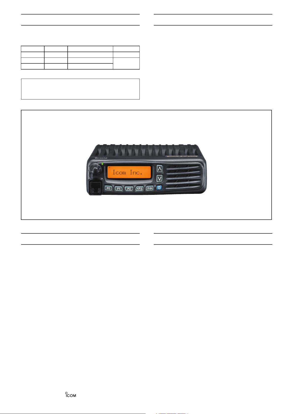
MODEL VERSION CHANNEL SPACING TX POWER
IC-F5061 USA-01 15.0/30.0 kHz 50 W
IC-F5062 EXP-01 12.5/25.0 kHz
IC-F5063 EUR-01 12.5/20/25.0 kHz
To upgrade quality, any electrical or mechanical parts and
internal circuits are subject to change without notice or
obligation.
25 W
NEVER connect the transceiver to an AC outlet or to a DC
power supply that uses more than 15 V. This will ruin the
transceiver.
DO NOT expose the transceiver to rain, snow or any liquids.
DO NOT reverse the polarities of the power supply when
connecting the transceiver.
DO NOT apply an RF signal of more than 20 dBm (100 mW)
to the antenna connector. This could damage the transceiver’
s front end.
ORDERING PARTS
Be sure to include the following four points when ordering
replacement parts:
1. 10-digit Icom parts numbers
2. Component part number and name
3. Equipment model name and unit name
4. Quantity required
<SAMPLE ORDER>
1110003491 S.IC TA31136FNG IC-F5061 MAIN UNIT 5 pieces
8820001210 Screw 2438 screw IC-F5062 Top cover 10 pieces
Addresses are provided on the inside back cover for your
convenience.
REPAIR NOTES
1. Make sure a problem is internal before disassembling
the transceiver.
2. DO NOT open the transceiver until the transceiver is
disconnected from its power source.
3. DO NOT force any of the variable components. Turn
them slowly and smoothly.
4. DO NOT short any circuits or electronic parts. An
insulated tuning tool MUST be used for all adjustments.
5. DO NOT keep power ON for a long time when the
transceiver is defective.
6. DO NOT transmit power into a signal generator or a
sweep generator.
7. ALWAYS connect a 50 dB to 60 dB attenuator between
the transceiver and a deviation meter or spectrum
analyzer when using such test equipment.
8. READ the instructions of test equipment thoroughly
before connecting equipment to the transceiver.
Icom, Icom Inc. and
Kingdom, Germany, France, Spain, Russia and/or other countries.
logo are registered trademarks of Icom Incorporated (Japan) in the United States, the United
Page 3

CONTENTS
SECTION 1 SPECIFICATIONS
SECTION 2 INSIDE VIEWS
SECTION 3 DISASSEMBLY INSTRUCTIONS
SECTION 4 OPTIONAL UNITS INSTALLATIONS
SECTION 5 CIRCUIT DESCRIPITON
5-1 RECEIVER CIRCUITS. . . . . . . . . . . . . . . . . . . . . . . . . . . . . . . . . . . . . . . . . . . . . . . . . . . . . . . . 5-1
5-2 TRANSMITTER CIRCUITS . . . . . . . . . . . . . . . . . . . . . . . . . . . . . . . . . . . . . . . . . . . . . . . . . . . . 5-2
5-3
5-4 POWER SUPPLY CIRCUITS. . . . . . . . . . . . . . . . . . . . . . . . . . . . . . . . . . . . . . . . . . . . . . . . . . . 5-4
5-5 PORT ALLOCATIONS . . . . . . . . . . . . . . . . . . . . . . . . . . . . . . . . . . . . . . . . . . . . . . . . . . . . . . . . 5-5
SECTION 6 ADJUSTMENT PROCEDURES
6-1 PREPARATION . . . . . . . . . . . . . . . . . . . . . . . . . . . . . . . . . . . . . . . . . . . . . . . . . . . . . . . . . . . . . 6-1
6-2 FREQUENCY ADJUSTMENT . . . . . . . . . . . . . . . . . . . . . . . . . . . . . . . . . . . . . . . . . . . . . . . . . . 6-2
6-3 TRANSMIT ADJUSTMENT . . . . . . . . . . . . . . . . . . . . . . . . . . . . . . . . . . . . . . . . . . . . . . . . . . . . 6-3
6-4 RECEIVE ADJUSTMENT . . . . . . . . . . . . . . . . . . . . . . . . . . . . . . . . . . . . . . . . . . . . . . . . . . . . . 6-4
FREQUENCY SYNTHESIZER CIRCUITS . . . . . . . . . . . . . . . . . . . . . . . . . . . . . . . . . . . . . . . . . 5-3
SECTION 7 PARTS LIST
SECTION 8 MECHANICAL PARTS AND DISASSEMBLY
SECTION 9 BOARD LAYOUTS
SECTION 10 BLOCK DIAGRAM
SECTION 11 VOLTAGE DIAGRAM
SECTION 12 HM-152
Page 4
SECTION 1 SPECIFICATIONS
[USA] [EXP] [EUR]
• Frequency coverage 136–174 MHz
• Type of emission Wide 16K0F3E (25.0 kHz)
Middle – 14K0F3E (20.0 kHz)
11K0F3E (12.5 kHz)
Narrow
• Number of programable channels max. 512 channels (128 zones)
• Antenna impedance
• Operating temperature range −30˚ to +60˚; −22˚F to +140˚F –25˚C to +55˚C
• Power supply requirement
GENERAL
(negative ground)
• Current drain
(approx.)
• Dimensions (projections not included)
Stand-by 300 mA
RX
Max.audio 1200 mA
TX
at 25 W 7 A
at 50 W 14 A
8K10F1E/D (12.5 kHz)
4K00F1E/D(6.25 kHz)
50 Ω (nominal)
13.6 V DC (nominal) 13.2 V DC (nominal)
160 (W) × 45 (H) × 150 (D) mm
; 2 3/32 (W) × 4 23/32 (H) × 1 9/32 (D) in
8K50F3E (12.5 kHz)
4K00F1E/D (6.25 kHz)
• Weight (with BP-231, approx.)
• Transmit output power 50 W 25 W
• Modulation Variable reactance frequency modulation
• Max. permissible deviation Wide ±5.0 kHz
Middle – ±4.0 kHz
Narrow ±2.5 kHz
• Frequency error ±1.0 ppm ±1.5 kHz
• Spurious emission
• Adjacent channel power Wide More than 70 dB
TRANSMITTER
• Audio harmonic distortion 3% typ. (with 1 kHz AF 40% deviation)
• FM hum and noise
(without CCITT filter)
• Limiting charact of modulation 70–100% of max. deviation
• Microphone impedance 600
• Receive system Double-conversion superheterodyne
• Intermediate frequencies 1st IF; 46.35 MHz, 2nd IF; 450 kHz
• Sensitivity
• Squelch sensitivity (at threshold) 0.25 µV typ.
• Adjacent channel
selectivity
RECEIVER
• Spurious response More than 85 dB (90 dB typ.)
• Intermodulation More than 75 dB (77 dB typ.) More than 65 dB (70 dB typ.)
• Hum and noise
(without CCITT filter)
• Audio output power 4 W typ. at 10% distortion with a 4 Ω load
• Audio output impedance 4
Measurements made in accordance with EIA-152-C/204D, TIA-603 ([USA],
All stated specifications are subject to change without notice or obligation.
Middle – More than 70 dB
Narrow More than 60 dB
Wide More than 40 dB (45 dB typ.) –
Narrow More than 34 dB (40 dB typ.) –
0.25 µV typ. at 12 dB SINAD
Wide More than 80 dB (85 dB typ.)
Middle − More than 78 dB (83 dB typ.)
Narrow More than 70 dB (75 dB typ.)
Wide More than 45 dB (50 dB typ.) –
Narrow More than 40 dB (45 dB typ.) –
75 dB typ.
[EXP]) or
1310 g; 2 Ib 14 oz
0.25 µW (≤1 GHz),
1.0 µW (>1 GHz)
Ω
−4 dBµV (EMF) typ.
at 20 dB SINAD
Ω
EN 300 086 ([EUR]).
1 - 1
Page 5
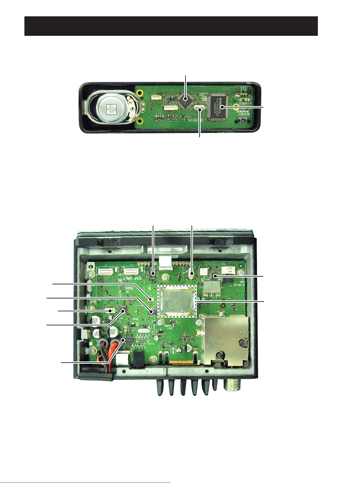
SECTION 2 INSIDE VIEWS
• FRONT UNIT
FRONT CPU
(IC503: HD64F3687)
FRONT CPU CLOCK
(X501: CR-764)
LCD DRIVER
(IC501: S1D15206F)
• MAIN UNIT
REF OSC
(X1: CR-826)
PLL IC
(IC4: LMX2352TM)
CPU CLOCK
(X5: CR-764)
AF LPF
(IC7: NJM12902V)
LEVEL CONV.
(IC19: DS14C232TM)
AF SWITCH/AMP
(IC1: NJM12902V)
BBIC CLOCK
(X2: CR-765)
IF IC
(IC170: TA31136FNG)
VCO
2 - 1
Page 6
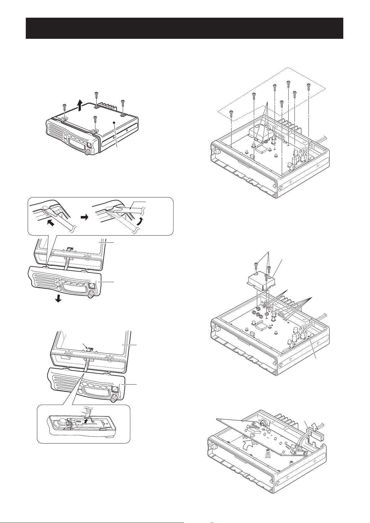
SECTION 3 DISASSEMBLY INSTRUCTION
1. Removing the front panel
q Turn the transceiver’s power OFF, then disconnect the DC
power cable
w Unscrew the 4 bottom screws, then remove the bottom
cover from the transceiver in the direction of the arrow.
Bottom cover
e Remove the front panel from the main body using a
standard cabinet screw driver as shown below.
Standard
screw driver
Main body
2. Removing the MAIN UNIT
q Unscrew 7 screws A, and unsolder 3 points B.
A
B
w Unscrew 3 screws C and remove the shield cover.
e Unsolder 3 points D (at the antenna connector) and
5 points E (at the PA module).
r Remove the clip.
C
Shield cover
Front panel
r Disconnect the flat cable from the front panel.
Flat cable
Flat cable
Front panel
Main body
Front panel
D
E
Clip
t Remove the bush, and remove the MAIN UNIT in the
direction of the arrow.
Bush
3 - 1
Page 7

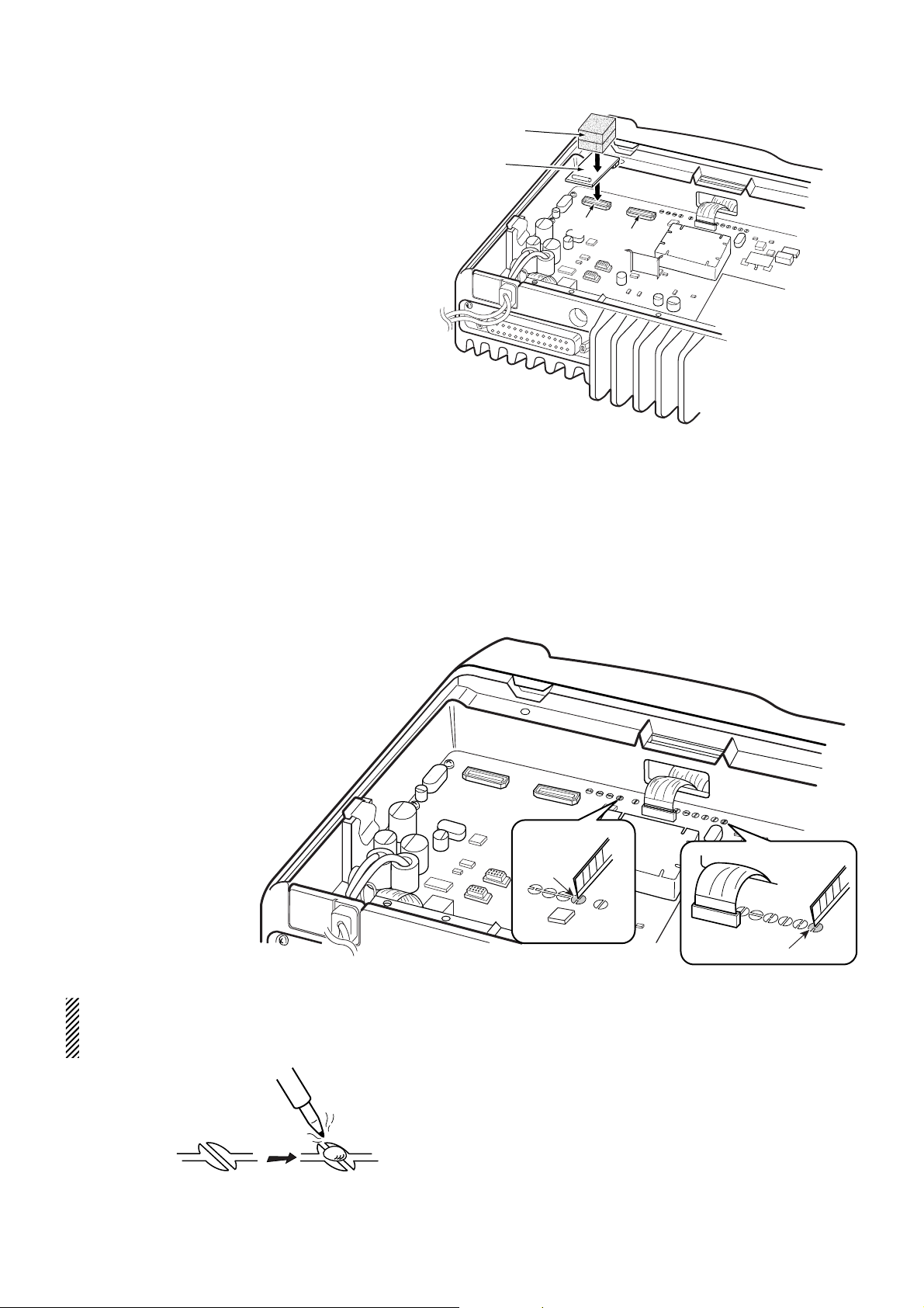
SECTION 4 OPTIONAL UNITS INSTALLATION
BEFORE INSTALLING OPTIONAL UNITS
P
A sponge with an adhesive strip has been added to optional units (UT-96R,
UT-108R, UT-109R, UT-110R, UT-119R, UT-119H, UT-124, UT-124R).
Remove the bottom protective papar, and attach the sponge to the specifi ed
position on the optional units as below.
• UT-96R • UT-108R/UT-124/UT-124R
Supplied sponge
• UT-109R/UT-110R • UT-119R
Supplied sponge
Supplied sponge
Supplied sponge
4 - 1
Page 8
Optional UT-96R or UT-119H installation
P
Install the optional UT-96R or UT-119H unit as follows:
Turn the power OFF, then disconnect the DC power cable.
q
Unscrew the 4 cover screws, then remove the bottom cover.
w
Install the UT-96R to J1 and the UT-119H to J2 as shown
e
in the diagram below.
Remove the protective paper from the supplied sponge,
r
then attach it on the installed unit.
Replace the bottom cover and screws, then re-connect
t
the DC power cable.
Sponge
UT-96R
J1
J2
*This illustration describes the UT-96R installation.
Front panel
Optional UT-109R or UT-110R installation
P
Turn the power OFF, then disconne ct the DC power cable.
q
Unscrew the 4 cover screws, then remove the bottom cover.
w
Cut the pattern on the PCB at the A (MIC) and B (AF OUT)
e
as shown below.
Install the scrambler unit to J1 as described in the instal-
r
lation of optional UT-96R installation as above.
Remove the protective paper from the supplied sponge,
t
then attach it on the installed unit.
Replace the bottom cover and screws.
y
Front panel
A
B
NOTE: When uninstalling the unit
Be sure to re-solder the disconnected points as below
when you remove the unit. Otherwise no TX modulation or
AF output is available.
Re-solder
4 - 2
Page 9
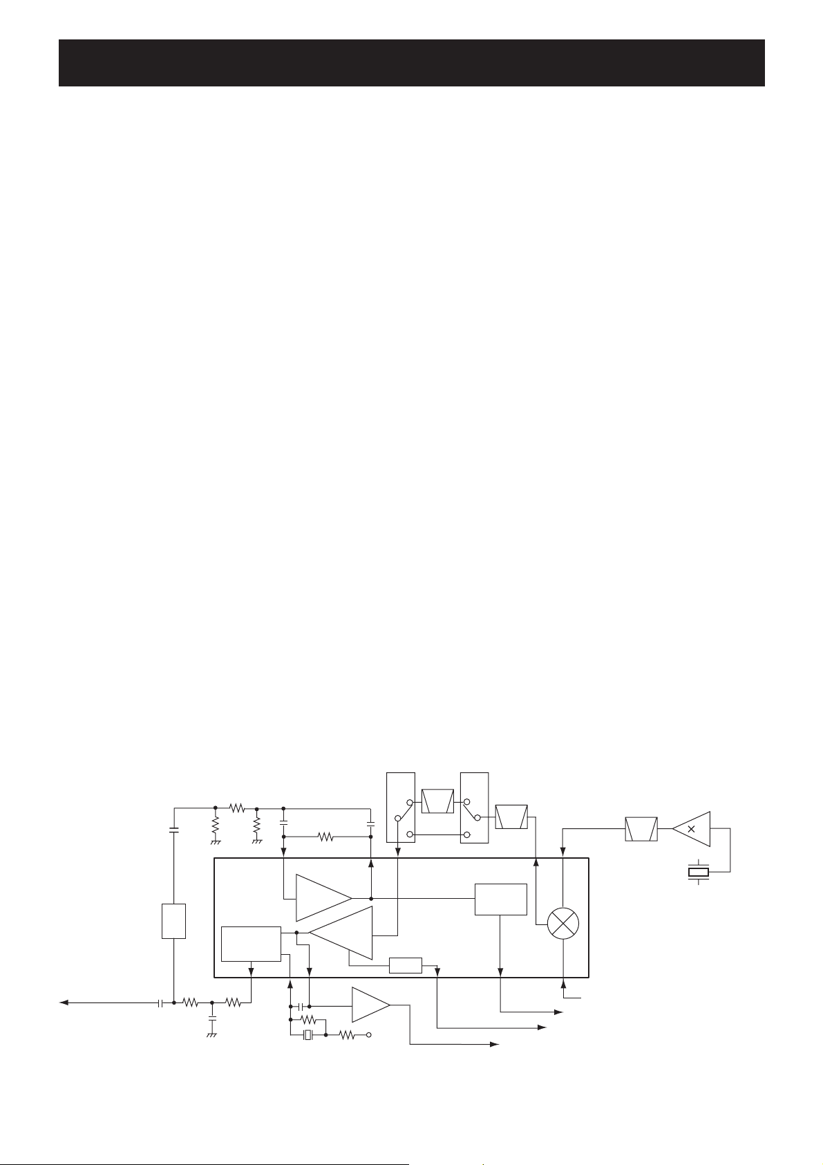
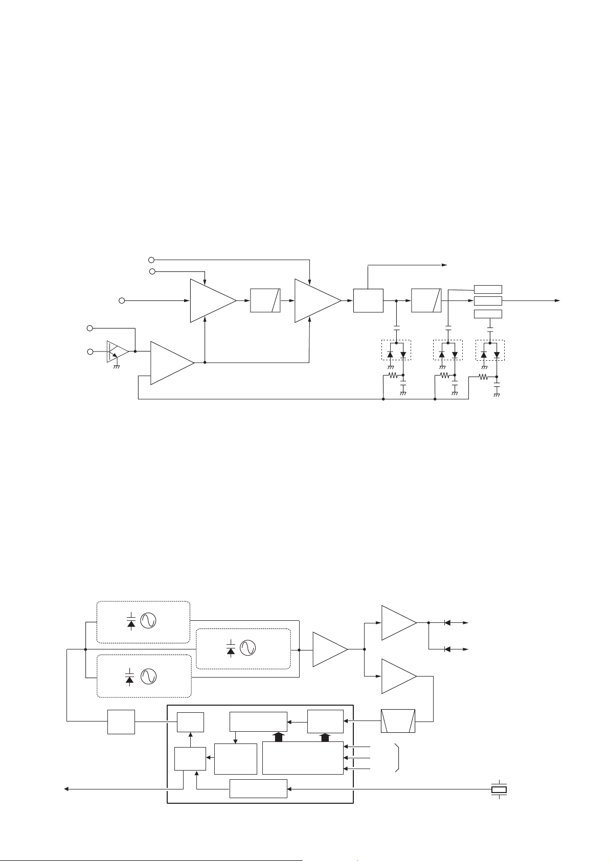
SECTION 5 CIRCUIT DESCRIPTION
5-1 RECEIVER CIRCUITS
RF CIRCUITS
The antenna switching circuit toggles between the receive
(RX) line and transmit (TX) line. RF amplifi er
received signals within the frequency coverage.
Received signals from the antenna are passed through Low
Pass filter (LPF; L40, C369, C370), TX power detector (D47,
D49, D51) and another LPF (L38, L39, C343, C345, C356,
C357), then applied to the antenna switching circuit (D38/
D39, L37, C337, C346).
The received signals are passed through the antenna
switching circuit as an LPF (L37, C337, C346), LPF (L35,
C322, C322, C323, C336) and two-staged tuned Bandpass
Filter (BPF; D34, L32, C299, C300 and D31, L31, C278,
C279), then applied to the RF amplifier (Q31).
The amplified signals are passed through another twostaged tuned BPF (D27, L28, C260−C263, C242 and D26,
L26, C219, C220, C240) and applied to the 1st mixer (IC10;
pins 4, 5, L18, L19, L24).
1ST IF CIRCUITS
The amplified received signals from the RF circuit are
converted into the 1st IF signal, fi ltered and amplifi ed at the
1st IF circuits.
The received signals from the RF circuits are mixed with
1st Local Oscillator (LO) signal from the RX VCOs, to be
converted into the 1st IF signal. The converted 1st IF signal
is amplified by 1st IF amplifier (Q50). The amplified 1st IF
signal is passed through the 1st IF filter (FI3 for analog
mode, FI4 for digital mode) via filter switches (Q20, D21,
D66, D67 on input side; D6, D68, D69 on output side) to
suppress unwanted signals. The filtered 1st IF signal is
amplified by another 1st IF amplifier (Q12), then applied to
the 2nd IF circuits.
2ND IF CIRCUITS
The 1st IF signal is converted into the 2nd IF signal,
amplified and demodulated in the IF IC.
amplifi es the
The 1st IF signal from the 1st IF amplifier (Q12) is applied
to the IF IC (IC5, pin 16). The applied signal is converted
into the 2nd IF signal by being mixed with the 2nd LO signal
from X1 via tripler (Q3, L3, L2, C32−C35).
The converted 2nd IF signal is output from pin 3, and
passed through the 2nd IF filter (FI1). The filtered 2nd IF
signal is passed through (bypassed) another 2nd IF filter
(FI2) via filter switches (D1 on input side; D2 on output
side). The filtered signal is then applied to the IF IC (IC5, pin
5), and amplified by 2nd IF amplifier. The amplified signal is
FM-demodulated by quadrature detector (IC5, pins 10, 11;
X3).
The demodulated AF signals are output from pin 9, then
applied to the AF circuits.
AF CIRCUITS
The demodulated AF signals from the IF IC are amplified
and fi ltered at AF circuits.
This transceiver employs the base band IC for audio signal
processing for both transmit and receive. The base band
IC is an audio processor and composed of pre-amplifier,
compressor, expander, scrambler, etc. in its package.
The demodulated AF signals from IF IC (IC5, pin 9) are
passed through Digital/Analog switch (IC8, pins 2, 15), and
applied to the base band IC (IC2, pin 23).
The applied AF signals are amplified at the amplifier section
and level adjusted at the volume controller section, then
suppressed unwanted 3 kHz and higher audio signals at
LPF. The filtered AF signals are applied (bypassed) the TX/
RX HPF, scrambler, de-emphasis sections in sequence.
The TX/RX HPF filters out 250 Hz and lower audio signals,
and the de-emphasis circuit obtains –6 dB/oct of audio
characteristics. The expander expands the compressed
audio signals and also noise reduction function is provided.
The AF signals are then level adjusted at the volume
controller section and amplified at the amplifier section, then
output from pin 20 (IC2).
• 2nd IF AND DEMODULATOR CIRCUITS
2
D/A converter
Demodulated signals
to the AF circuits
(IC6)
1
Quadrature
detector
9
8
Filter
amp.
1110
X3
Limiter
amp.
Buffer
D2
N/W
SW
735
Q13
+5V
RSSI
5 - 1
FI2
D1
N/W
SW
FI1
Noise
detector
Mixer
45.9 MHz
2
BPF
IF IC (IC5)
1312
“D_IF” signal to the optional digital unit via J2
16
1st IF signal from the IF amplifier (Q12)
“NOIS” signal to the CPU (IC14: pin 113)
“RSSI” signal to the CPU (IC14: pin 71)
Q3
3
X1
15.3 MHz
Page 10
The processed AF signals from the base band IC (IC2) are
passed through the AF mute switch (IC8, pins 3, 4) and D/A
converter (IC6, pins 15, 16) for level adjustment. The level
adjusted AF signals are amplified by AF amplifier (IC22).
The amplified AF signals are then;
- Output from D-sub 25 pin connector (CONNECT UNIT;
J602).
or
- Buffer-amplified by Q49, then applied to connected micro phone via FRONT UNIT.
or
- Applied to the AF power amplifier (IC21, pin 1) to obtain AF
output power level, then applied to the internal/external
speaker via external speaker jack (J7).
5-2 TRANSMITTER CIRCUITS
MICROPHONE AMPLIFIER CIRCUITS
The AF signals from the microphone (MIC signals) are
filtered and level-adjusted at the microphone amplifier
circuits.
AF signals from the connected microphone (MIC signals)
are passed through (bypassed) the ALC (Automatic Level
Control) amplifier (FRONT UNIT; IC505, pins 3, 5) via AF
switch (FRONT UNIT; IC507, pins 1, 6/7), then applied to
the microphone amplifier (FRONT UNIT; IC508, pin 3). The
amplified MIC signals are output from pin 4, and applied to
the MAIN UNIT.
The MIC signals from the FRONT UNIT are passed through
the Int./Ext. MIC switch (IC23, pins 1, 6), and applied to the
base band IC (IC2, pin 3) and processed.
SQUELCH CIRCUITS
<NOISE SQUELCH>
The squelch mutes the AF output signals when no RF signals
are received. By detecting noise components (30 kHz and
higher signals) in the demodulated AF signals, the squelch
circuit toggles the AF power amplifi er ON and OFF.
A portion of the demodulated AF signals from the IF IC
(IC5, pin 9) are applied to the D/A converter (IC6, pin 1)
for level adjustment (squelch threshold adjustment). The
level-adjusted AF signals are output from pin 2 and passed
through the noise filter (IC5, pins 7, 8, R121−R124, C216
−C218). The filtered noise signals are amplified the noise
components only.
The amplifi ed noise components are converted into the pulsetype signal at the noise detector section, and output from pin
13 as the “NOIS” signal. The “NOIS” signal is applied to the
CPU (IC14, pin 113), Then the CPU outputs signal “AFON2”
signal from pin 15 to the AF power amplifier controller (Q51,
Q52, D65), according to the “NOIS” signal level. The AF power
amplifi er controller toggles AF power amplifi er (IC21) ON and
OFF according to the “AFON” signal.
<TONE SQUELCH>
The tone squelch circuit detects tone signals and opens the
squelch only when receiving a signal containing a matched
sub audible tone. When the tone squelch is in use, and a
signal with a mismatched or no sub audible tone is received,
the tone squelch circuit mutes the AF signals even when the
noise squelch is open.
• CTCSS/DTCS
A portion of the demodulated AF signals are passed through
the active LPF (Q4, R45, R46, R47, R63, R64, C45, C46,
C47, C71) to filters CTCSS/DTCS signal. The filtered signal
is applied to the CPU (IC14, pin 64). The CPU compares the
applied signal and the set CTCSS/DTCS, then outputs control signal as same as “NOISE SQUELCH.”
• 2/5 TONE AND DTMF
2/5 tone signals in the demodulated AF signals are passed
through the LPF in the base band IC (IC2) and output from
pin 21, then applied to the CPU (IC14, pin 63) via tone
amplifer (IC1, pins 8, 9), and decoded.
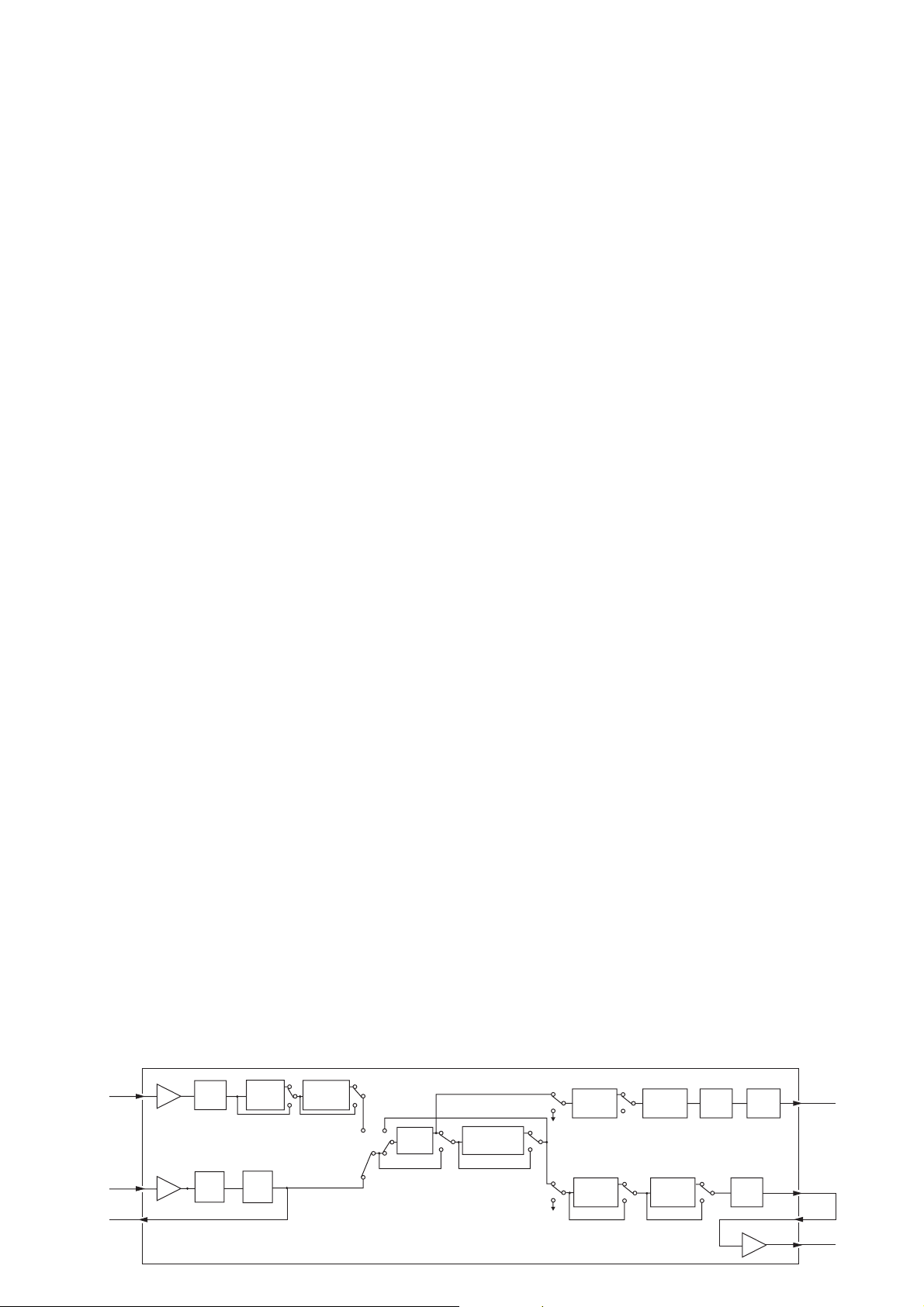
• BASE BAND IC BLOCK DIAGRAM
The applied MIC signals are amplifi ed at the amplifi er (TXA1),
and level adjusted at the volume controller (VR1). The level
adjusted MIC signals are applied (bypassed) the compressor
section, pre-emphasis section, TX/RX HPF, de-scrambler, limiter,
splatter, in sequence, then applied to another volume controller.
The compressor compresses the MIC signals to provide high S/N
ratio for receive side, and the pre-emphasis obtains +6 dB/oct
audio characteristics. The TX/RX HPF filters out 250 Hz and
lower audio signals, the limiter limits its level and the splatter
filters out 3 kHz and higher audio signals. The filtered MIC
signals are level adjusted at another volume controller (VR2),
and then output from pin 7 via smoothing fi lter (SMF).
The MIC signals from the base band IC are passed through
the digital/analog switch (IC8, pins 12, 14), FM/PM switch
(IC3, pins 13, 14), and applied to the AF mixer (IC1, pin
13) where the MIC signals and tone signals are mixed with.
The mixed MIC signals are passed through D/A converter
(IC6, pins 3, 4) for level adjustment. The level adjusted MIC
signals are then applied to the VCO as modulation signals.
MODULATION CIRCUITS
The modulation circuits modulates the VCO oscillating signal
using the modulation signals.
The MIC signals from the microphone amplifier circuits are
applied to the D20 of TX VCO (Q19, D14, D17, D18, D20)
as the modulation signals, and modulate the VCO oscillating
signal by changing the reactance of D20.
The FM-modulated VCO output is amplified by bufferamplifiers (Q22, Q29), then applied to the power amplifiers
via D24 as the TX signal.
SIGNALING ENCODE
5/2-TONE, DTMF and CTCSS/DTCS signals are output
from the CPU (IC14) and passed through the LPF (IC7)
and level converter (IC6), then applied to the AF mixer
(IC1, pin 13) and mixed with MIC signals. The mixed tone
signals are passed through the D/A converter (IC6, pins 3,
4) for level adjustment. The level adjusted tone signals are
applied to the both of TX VCO (Q19, D14, D17, D18, D20)
and reference frequency oscillator (X1, pin 1) via the level
adjuster (IC1, pins 1, 3).
BASE BAND IC (IC2)
Com-
pressor
RX
LPF
Pre-
emphasis
TX/RX
HPF
Scrambler/
De-scrambler
Limiter Splatter VR2
De-
emphasis
Expander
VR4
SMF
RXA2
7 MOD
18
19
20
SIGNAL
TXA1
RXA1
VR1
(HPF)
VR3
(HPF)
3TXIN
23RXIN
21SDEC
5 - 2
Page 11
TX POWER AMPLIFIERS
The transmit signal from the TX VCO is amplified to the
transmit output level by the transmit amplifi ers.
The TX VCO output signal from buffer amplifier (Q29) is
applied to the YGR amplifier (Q30) via the TX/RX switch
(D24). The amplified TX signal is passed through the LPF
(L29, L30, C269−C271, C290), and applied to the RF power
module (IC15, pin 1) and power-amplified to obtain 50 W/25
W (max.) of TX output power.
The power-amplified TX signal is passed through the LPF as
a harmonic filter (L33, C305−C308), the antenna switching
circuit (D38, D39) and LPF (L38, L39, C343, C345, C356,
C357).
The TX signal is also gone through the power detector (D47,
D49, D51) and LPF (L40, C369, C370) before being applied
to the antenna connector.
• APC CIRCUIT
APC CIRCUIT
The APC (Automatic Power Control) circuit prevents the
transition of the transmit output power level which is caused
by load mismatching or heat effect, etc. At the power
detector, a portion of the transmit signal is rectified to
produce DC voltage which is in proportion of the transmit
power level.
The rectified voltage is applied to the inverted input terminal
of the operational amplifier (IC17, pin 3). The TX power
setting voltage “T2” from the D/A converter (IC12, pin 2) is
applied to the non-inverted input terminal as the reference.
The operational amplifier compares the rectified voltage and
reference voltage “T2,” and the difference of the voltage is
output from the operational amplifier pin 4, and the output
voltage controls the bias of YGR (Q30) amplifier and power
module (IC15) for stable transmit output power.
HV
T8V
Q30
IC17
YGR
amp.
LPF
Transmit signal
from TX/RX switch (D24)
“T2”
Q53
“TMUT”
+
OP.
amp.
–
5-3 FREQUENCY SYNTHESIZER CIRCUITS
VCO
VCO is a oscillator whose oscillating frequency is controlled
by adding voltage (lock voltage).
• RX VCO1 (Q18, D10, D13)
RX VCO1 generates the 1st LO signal for receiving 155−174
MHz signals.
• RX VCO2 (Q17, D8, D9)
RX VCO2 generates the 1st LO signal for receiving 136−155
MHz signals.
to the 1st mixer (IC10)
IC15
Powe r
amp.
ANT
SW
D47
LPF
D49
to the antenna
D51
Each output signals are amplified by the buffer amplifiers
(Q22, Q29), and applied to the 1st mixer (IC10, pins 4, 5) via
TX/RX switch (D25 is ON, D24 is OFF) and LPF (L22, L23,
C215, C216, C236, C237), to be mixed with the received
signals to produce the 46.35 MHz 1st IF signal.
• TX VCO (Q19, D14, D17, D18, D20)
The output signal is applied to the transmit amplifi ers via the
buffer amplifi ers (Q22, Q29) and TX/RX switch (D24 is ON,
D25 is OFF).
A portion of the buffer-amplified VCO output signals from the
buffer amplifier (Q22) are applied to the PLL IC (IC4, pin 6)
via doubler (Q25) and BPF (Q5, D4, D5, L4, R77, C84−C90).
• PLL CIRCUITS
RX VCO1 (155–174 MHz)
Q18, D10, D13
RX VCO2 (136–155 MHz)
Q17, D8, D9
Loop
filter
PLL unlock signal
to the CPU (IC14, pin 73)
11
4
TX VCO
Q19, D14, D17, D18, D20
Charge
pump
Phase
detector
Programmable
Divide
ratio
adjustment
divider
Reference
divider
Buffer
Q22
PLL IC (IC4)
Prescaler
Shift register
5 - 3
Buffer
Q29
×3
Q25
6
14
15
16
10
BPF
SCK
SSO
PLL control signals from the CPU (IC14)
PLST
15.3 MHz
reference frequency signal
D14
to transmitter circuit
D15
to 1st mixer circuit
X1
15.3 MHz
Page 12

PLL IC
The PLL circuit provides stable oscillation of the transmit
frequency and receive 1st LO frequency. The PLL output
frequency is controlled by the divided ratio (N-data) from the
CPU.
The phase difference is output from pin 4 as a pulse type
signal after being passed through the internal charge pump.
The output signal is converted into the DC voltage (lock
voltage) by passing through the loop filter (Q8, Q9). The lock
voltage is applied to the variable capacitors (D10 and D13
of RX VCO1, D8 and D9 of RX VCO2, D14 and D17 of TX
The applied signals are divided at the prescaler and
VCO), and locked to keep the VCO frequency constant.
programmable counter according to the control signals
(“SSO,” “PLST” and "SCK”) from the CPU. The divided signal
is phase-compared with the reference frequency signal from
the reference frequency oscillator (X1, pin 3), at the phase
If the oscillated signal drifts, its phase changes from that of
the reference frequency, causing a lock voltage change to
compensate for the drift in the VCO oscillating frequency.
detector.
5-4 POWER SUPPLY CIRCUITS (MAIN UNIT)
Voltage from the attached battery pack is routed to whole of the circuit in the transceiver via switches and regulators.
• POWER SUPPLY CIRCUITS
CPU (IC14),
EEPROM (IC16),
etc.
RF power amplifier (IC15)
AF power amplifier (IC21)
etc.
etc.
Transmitter circuits
Common circuits
Receiver circuits
PLL IC (IC4)
Attached optional units,
D/A converters,
etc.
R8V
+5V
Q38, Q39
R8V
regurator
+5V
regurator
Q35, Q36
HV
T8V
+8V
T8V
regurator
Q34, Q37, D37
+8V
regurator
IC20
“RXC”
CPU5
VCC
47
IC18
CPU5
regurator
Q47, Q48
Power switch
“PWON”
“TXC”
4146
(IC14)
CPU
HV
Control signal
Power Supply
Voltage line
5 - 4
Page 13

5-5 PORT ALLOCATIONS
• CPU (MAIN UNIT; IC14)
Pin
Port
No.
Name
1 DSDA Outputs serial data to the D/A converter (IC20, pin 6).
2 DAST Outputs strobe signal to the D/A converter (IC4, pin 6).
3 SIDE3
4−7 CBI0−3 Input ports for [ROTARY SELECTOR] (S701).
10 SSO
11 SCK
13 PLST
15 DASW
17 TMUT
18 NWC2
19 NWC1
20 DDSD
21 DDAC
26 T5C
27 R5C
28 S5C
29 PTTSW
30 SIDE2
32 RMUT Outputs mute signal to the AF mute switch (D42).
37 NOIS
38 POSW
39 DDST
40 MTCK
41 PWON
43 SENC
44 BEEP Outputs beep sound to the AF circuits (IC4, pin 13).
45 SDEC Input port for decoded 2/5 tone and DTMF signals.
46 CDEC Input port for decoded CTCSS/DTCS signal.
47 ISENS
48 BATV Input port for remaining battery power.
49 LVIN Input port for VCO lock voltage.
50 RSSI
55 EMER Input port for [Emer] switch (S702).
Input port for [Side3] key (S4).
"Low"=When the key is pushed.
Outputs serial data to the PLL IC (IC1, pin 15), D/A
converter (IC4, pin 8).
Outputs serial crock signal to the PLL IC (IC1, pin
14), D/A converter (IC4, pin 8).
Outputs PLL strobe signal to the PLL IC (RF UNIT;
IC1, pin 16).
Outputs mode (Digital/Analog) switching signal to
the D/A converter (IC14, pins 10, 11).
Outputs transmit mute signal to the transmit mute
switch (RF UNIT; Q606).
Outputs Narrow/Wide mode switching signal to the
bandwidth switches (Q26, D32, D33).
Outputs Narrow/Wide mode switching signal to the
bandwidth switches (Q27, Q41, Q42, D34, D35).
Outputs serial data to the DTMF decode IC (IC10,
pin 9).
Outputs serial clock signal to the DTMF decode IC
(IC10, pin 11).
Outputs T5V line control signal to the T5V regulator
(Q15).
"Low"= While transmitting.
Output R5V line control signal to the R5V regulator
(Q16).
"Low"= While receiving.
Output S5V line control signal to the S5V regulator
(Q14).
"Low"=While power save mode.
Input port for [PTT] switch (S3).
"Low"=When the switch is pushed.
Input port for [Side2] key (S5).
"Low"=When the key is pushed.
Input port for the noise level from the IF IC (IC3, pin
13).
Input port for power switch (R702) from power
controller (D36).
Outputs strobe signal to the DTMF decode IC (MAIN
UNIT; IC10, pin 14).
Outputs serial clock signal to the base band IC
(MAIN UNIT; IC5, pin 9).
Outputs VCC line control signal to the power switch
(Q30, Q31).
"Low"=While the power is ON.
Outputs single tone encode signal to the LPF (IC17,
pin 10).
Input port for power amplifier current detect signal
from the current detector (RF UNIT; Q604, Q605).
Input port for RSSI signal from the IF IC (IC3, pin
12).
Description
Pin
Port
No.
Name
70 CSFT
71 DUSE
73 UNLK
74 RLED
75 TLED
78 FSDA
79 FSCL
81 CIRQ
88 SIDE1
CENC0−
89−
91
92 EMPH
93 MTDT Outputs serial data to the base band IC (IC5, pin 10).
96 MSCK
97 PMFM
98 ESDA Outputs serial data to the EEPROM (IC19, pin 5).
99 ESCL
100 RESL Input port for reset signal from the reset IC (IC8, pin 1).
Outputs CPU clock frequency shift signal to the CPU
clock oscillator (X2, D38).
Outputs CTCSS/DTCS select signal to the CTCSS/
DTCS switch (Q34).
Input port for PLL unlock detect signal from the PLL
IC (IC1, pin 11).
Outputs RX indicator (DS701) control signal to the
LED driver (Q701).
Outputs TX indicator (DS701) control signal to the
LED driver (Q701).
Outputs serial data to the expand IC (FRONT UNIT;
IC505, pin 3).
Outputs serial clock signal to the expand IC (FRONT
UNIT; IC505, pin 3).
Input port for external connection detect signal from
J1 and J2.
Input port for [Side1] key (S6).
"Low"=When the key is pushed.
Output CTCSS/DTCS signals to the LPF (IC17, pin 3).
2
Outputs emphasis characteristic change signal to
the D/A converter (IC13, pins 9, 10).
Outputs serial clock signal to the base band IC
(MAIN UNIT; IC5, pin 13).
Outputs modulation mode switching signal to the
PM/FM switch (IC13, pin 11) .
Outputs serial clock signal to the EEPROM (IC19,
pin 6).
Description
• D/A CONVERTER (MAIN UNIT; IC6)
Pin
Port
No.
Name
1T1
2T2
3 TXLVA
4 RXLVA
Outputs BPF tuning voltage to the tunable BPF (
D24, L31, L32, C120−C122, C125−C127
• While receiving
Outputs BPF tuning voltage to the tunable BPF
(
D28, D29, L33, L34, C140−C144, C147).
• While transmitting
Outputs TX power setting voltage to the APC
amplifi er (RF UNIT; IC601).
Outputs oscillation frequency adjust voltage to the
TX VCO (
Outputs oscillation frequency adjust voltage to the
RX VCO1/2 (
Q3, D10−D12).
Description
D23,
).
Q1, D1−D4/Q2, D5−D8).
5 - 5
Page 14

SECTION 6 ADJUSTMENT PROCEDURES
6-1 PREPARATION
When adjusting IC-F5060 series transceiver, CS-F5060
,
er), RS-232C cable
JIG cable (modifi ed OPC-1122/U
CLONING SOFTWARE,
CLONING CABLE
; see the page 6-2) and the following test equipments are required.
CS-F5060 ADJ
EQUIPMENT GRADE AND RANGE EQUIPMENT GRADE AND RANGE
DC power supply
Output voltage
Current capacity
modulation analyzer
Frequency counter
RF power meter
▄
SYSTEM REQUIREMENTS
• Microsoft
®
Windows® 98/98SE/Me/2000/XP • RS-232C serial port (D-sub 9 pin)
Frequency range
Measuring range
Frequency range
Frequency accuracy
Sensitivity
Measuring range
Frequency range
Impedance
SWR
: 13.6 V DC [USA]
13.2 V DC [EUR], [EXP]
: More than 1.5 A
: DC–300 MHz
: 0 to ±10 kHz
: 0.1–300 MHz
: ±1 ppm or better
: 100 mV or better
: 0.1–60 W [USA]
0.1–30 W [EUR], [EXP]
: 100–300 MHz
: 50
Ω
: Better than 1.2 : 1
Attenuator
External speaker
Standard signal
generator (SSG)
Oscilloscope
Digital voltmeter
(for the ADJUSTMENT SOFTWARE)
ADJUSTMENT SOFTWARE
Power attenuation
Capacity
Input impedance
Capacity
Frequency range
Output level
Frequency rang
Measuring range
Input impedance
Measuring range
: 50 or 60 dB
: 60 W [USA]
30 W [EUR], [EXP]
: 4
: 5 W or more
: 0.1–300 MHz
: 0.1 µV to 32 mV
(–127 to –17 dBm)
: DC–20 MHz
: 0.01–20 V
: 50 k
: 0.1–10V
(Rev. 1.0 or lat-
Ω
Ω
▄
ADJUSTMENT SOFTWARE INSTALLATION
Quit all applications when Windows is running.
q
Insert the CD into the appropriate CD drive.
w
Double-click the “Setup.exe” contained in the ‘CS-F5060
e
ADJ’ folder in the CD drive.
The “Welcome to the InstallShield Wizard for CS-F5060
r
ADJ” will appear. Click [Next>].
The “Choose Destination Location” will appear. Then click
t
[Next>] to install the software to the destination folder. (e.g.
C:\Program Files\Icom\CS-F5060 ADJ)
After the installation is completed, the “InstallShield Wiz-
y
▄
STARTING SOFTWARE ADJUSTMENT
Connect the transceiver and PC with RS-232C cable and
q
JIG CABLE
Turn the transceiver power ON.
w
Boot up Windows, and click the program group ‘CS-F5060
e
.
ADJ’ in the ‘Programs’ folder of the [Start] menu, then
CS-F5060 ADJ’s window appears.
Click ‘Connect’ on the CS-F5060 ADJ’s window, then the
r
window shows transceiver’s condition and adjustment
items as below.
Set or modify adjustment data as specifi ed.
t
ard Complete” will appear. Then click [Finish].
Eject the CD.
u
Program group ‘CS-F5060 ADJ’ appears in the ‘Programs’
i
folder of the start menu, and ‘CS-F5060 ADJ’ icon appears on the desk top screen.
▄
BEFORE STARTING SOFTWARE ADJUSTMENT
Clone the adjustment frequencies and settings into the transceiver, and set the confi guration using the CS-F5060
WARE
before starting the software adjustment. Otherwise, the software adjustment can not be started.
Microsoft and Windows are registered trademarks of Micro-
soft Corporation in the U.S.A. and other countries.
CLONING SOFT-
CAUTION!: BACK UP the originally programmed memory data in the transceiver before programming the adjustment frequencies.
When program the adjustment frequencies into the transceiver, the transceiver’s memory data will be overwritten and
lose original memory data at the same time.
• ADJUSTMENT FREQUENCY LIST
CH FREQUENCY SETTING CH FREQUENCY SETTING
1 154.900 MHz
2 174.000 MHz
3 136.000 MHz
4 155.000 MHz
5 136.000 MHz
6 136.000 MHz
7 155.000 MHz
8 155.000 MHz
9 136.000 MHz
*; [EUR] only
• TX power
• Mode
• TX power
• Mode
• TX power
• Mode
• TX power
• Mode
• TX power
• Mode
• TX power
• Mode
• TX power
• Mode
• DTCS
• TX power
• Mode
• TX power
• Mode
: Low1
: Narrow
: Low1
: Wide
: Low1
: Wide
: Low1
: Wide
: High
: Narrow
: Low2
: Wide
: Low1
: Middle
: 007
: Low1
: Narrow
: Low1
: Narrow
10 174.000 MHz
11* 155.000 MHz
12* 136.000 MHz
13* 174.000 MHz
14 155.000 MHz
15 136.000 MHz
16 174.000 MHz
17 136.000 MHz
18 136.000 MHz
• TX power
• Mode
• TX power
• Mode
• TX power
• Mode
• TX power
• Mode
• TX power
• Mode
• TX power
• Mode
• TX power
• Mode
• TX power
• CTCSS
• TX power
• Mode
• DTMF
: Low1
: Narrow
: Low1
: Middle
: High
: Middle
: Low2
: Middle
: Low1
: Digital
: Low1
: Digital
: Low1
: Digital
: Low1
: 151.4 Hz
: Low1
: Wide
: P3
6 - 1
Page 15

• CONNECTION
CAUTION:
DO NOT transmit while
SSG is connected to
the antenna connector.
to an RS-232C port
RS-232C cable
(straight)
AC millivoltmeter
Audio generator
Standard signal generator
–127 to –17 dBm
(0.1 V to 32 mV)
Modulation analyzer
Attenuator
50 dB or 60 dB
OPC-1122U (USB type)
JIG CABLE
PC
JIG CABLE
RF power meter (50 Ω)
1–60 W [USA]
1–30 W [EUR], [EXP]
Frequency
counter
to the antenna connector
to the
[MICROPHONE CONNECTOR]
DC power supply
13.6 (13.2) V / 20 A [USA]
13.2 (13.2) V / 20 A [EUR], [EXP]
SINAD meter
SP (4 Ω)
to EXT. SP jack
to DC cable
IC-F5061
IC-F5062
IC-F5063
• JIG CABLE
(USB type Cloning cable)
Add a jumper wire here
OPC-1122
(RS-232C type Cloning cable)
OPC-1122U
PTTE
PTT
MIC
MICE
Electrolytic
capacitor
47 µF
PTT switch
+
Audio generator
300 Hz to 3 kHz
AC
millivoltmeter
Add a jumper wire here
GND
MIC
GND
PTT
6 - 2
+
PTT switch
Electrolytic
capacitor
47 µF
Audio generator
300 Hz to 3 kHz
AC
millivoltmeter
Page 16

• ADJUSTMENT SOFTWARE WINDOW
Transmit output power
(*)
Modulation balance
(*)
(*)
FM deviation
(*)
CTCSS/DTCS deviation
Squelch level
Reference frequency
RX sensitivity (Auto.)
RX sensitivity (Manu.)
(*)
PLL lock Voltage
(Adjustment)
PLL lock Voltage
(Preset)
S-meter
FM deviation
(Narrow)
FM deviation
(Middle)
*; DO NOT put the cursor on these items
FM deviation
(Wide)
Digital deviation
Digital mode preset
2/5tone, DTMF
and push the [ENTER] key. Otherwise,
some adjustment items will not be ad justed properly.
NOTE: The above screen is an example only. Each transceiver has its own specific values for each setting.
6 - 3
Page 17

6-2 FREQUENCY ADJUSTMENT
Select an adjustment item using [↑] / [↓] keys, then set to the specifi ed value using [←] / [→] keys on the connected PC’s keyboard.
ADJUSTMENT ADJUSTMENT CONDITION UNIT OPERATION VALUE
PLL LOCK
VOLTAGE
(adjustment)
[RX LVA1]
[RX LVA2] 3 • Channel
[TX LVA] 4 • Channel
PLL LOCK
VOLTAGE
(verify)
REFERENCE
FREQUENCY
[REF]
1 Set the preset value of [LV (RX1)], [LV (RX2)] and [LV (TX)] to “204 [4.00V]” on the adjustment software.
2 • Channel
• Receiving
• Receiving
• Transmitting
CONVENIENT:
1: Set the Lock voltage preset ([LV RX1], [LV RX2], [LV TX]) to “204 (4.00 V).”
2: Put the cursor on [RX LVA1], [RX LVA2] and [TX LVA], then push the [ENTER] key on the connected PC’s keyboard.
1 • Channel
• Receiving
2 • Channel
• Receiving
3 • Channel
• Transmitting
1 • Channel : CH 2 Top
• Connect an RF power meter to the
antenna connector.
• Transmitting
The “
: CH 1 PC
: CH 2
: CH 2
PLL LOCK VOLTAGE”
: CH 3 PC
: CH 4
: CH 3
Click [Reload (F5)] button, then
screen
screen
panel
check the “LVIN” item on the
CS-F5060 ADJ’s screen as below.
can be adjusted automatically.
Click [Reload (F5)] button, then
check the “LVIN” item on the
CS-F5060 ADJ’s screen.
Loosely couple a frequency
counter to the antenna connector.
4.00 V
0.8–1.6 V
(Verify)
174.000000 MHz
PLL LOCK VOLTAGE
will be appeared here
NOTE: The above screen is an example only.
Each item’s voltage will appear when pushing [Update] button.
6 - 4
Page 18

6-3 TRANSMIT ADJUSTMENT
Select an adjustment item using [↑] / [↓] keys, then set to the specifi ed value using [←] / [→] keys on the connected PC’s keyboard.
ADJUSTMENT ADJUSTMENT CONDITION UNIT OPERATION VALUE
OUTPUT
POWER
[Power (Hi)]
[Power (L2)] 2 • Channel : CH 6
[Power (L1)] 3 • Channel : CH 3
MODULATION
BALANCE
[BAL (Narrow)]
FM
DEVIATION
(NARROW)
[MOD N C]
[MOD N L] 2
[MOD N H] 3
(WIDE)
[MOD W C]
[MOD W L] 5
[MOD W H] 6
(MIDDLE)*
[MOD W C]
[MOD M L] 8
[MOD M H] 9
DIGITAL
DAVIATION
[MOD D C]
[MOD D L] 3
[MOD D H] 4
CTCSS/DTCS
DEVIATION
[CTCS/DTCS]
2TONE,
5TONE,
DTMF
[S.Tone]
*; [EUR] only.
1 • Channel : CH 5
• Transmitting
Rear
panel
Connect an RF power meter to
the antenna connector.
• Transmitting
• Transmitting
1 Set the preset value of [MOD N] to “100” on the adjustment software.
2 • Channel : CH 7
• No audio signals applied to the JIG cable.
• Set a modulation analyzer as;
HPF : OFF
Rear
panel
Connect the modulation analyzer with an oscilloscope to the
antenna connector through an
attenuator.
LPF : 20 kHz
De-emphasis : OFF
Detector : (P–P)/2
• Push [P0] while transmitting.
• Connect an audio generator to the JIG
1
cable and set as;
Frequency : 1.0 kHz
Rear
panel
Connect the modulation ana-
lyzer to the antenna connector
through an attenuator.
Level : 40 mV rms
• Set the modulation analyzer to the same
condition as “MODULATION BALANCE.”
• Transmitting
• Channel : CH 8
• Transmitting
• Channel : CH 9
• Transmitting
• Channel : CH 10
• Transmitting
• Channel : CH 4
4
• Transmitting
• Channel : CH 3
• Transmitting
• Channel : CH 2
• Transmitting
• Channel : CH 11
7
• Transmitting
• Channel : CH 12
• Transmitting
• Channel : CH 13
• Transmitting
Set the preset value of [Digital Mode] to “7” on the adjustment software.
1
• Attach the UT-119 to J2.
2
(Refer to page 4-2 for the installation)
• Channel : CH 14
Rear
panel
Connect the modulation ana-
lyzer to the antenna connector
through an attenuator.
• Transmitting
• Channel : CH 15
• Transmitting
• Channel : CH 16
• Transmitting
• Channel : CH 17
1
• No audio signals applied to the JIG cable.
• Set the modulation analyzer to the same
Rear
panel
Connect a modulation analyzer to
the antenna connector through
an attenuator.
condition as “MODULATION BALANCE.”
• Transmitting
• Channel : CH 18
1
• Transmitting
Rear
panel
Connect a modulation analyzer to
the antenna connector through
an attenuator.
50 W [USA]
[EUR], [EXP]
25 W
25 W [USA]
[EUR], [EXP]
10 W
5.0 W [USA]
[EUR], [EXP]
2.5 W
Set to square wave
form
±2.05 to ±2.15 kHz
±4.05 to ±4.15 kHz
±3.15 to ±3.25 kHz
±1.41 to ±1.45 kHz
±0.68 to ±0.72 kHz
1.50 kHz
±
6 - 5
Page 19

6-4 RECEIVE ADJUSTMENT
Select an adjustment item using [↑] / [↓] keys, then set to the specifi ed value using [←] / [→] keys on the connected PC’s keyboard.
ADJUSTMENT ADJUSTMENT CONDITION UNIT LOCATION VALUE
RECEIVE
SENSITIVITY
[BPF (T1) C]
[BPF (T2) C]
NOTE:
adjusted properly.
1
CONVENIENT:
The “RECEIVE SENSITIVITY” can be adjusted automatically.
1: Put the cursor on “[BPF C ALL]” and push [ENTER] key.
2: The connected PC tunes BPF’s to peak levels automaticaly.
S-METER
(S3 level)
[RSSI]
(S1 level)
SQUELCH
[SQL]
†;
The output level of the standard signal generator (SSG) is indicated as the SSG’s open circuit.
1
2
1 • Channel : CH 3
“RECEIVE SENSITIVITY” must be adjusted before “S-METER.” Otherwise, “S-METER” will not be
• Channel : CH 3
• Connect the SSG to the antenna connector and set as;
Frequency : 136.000 MHz
Level : +20 dBµ
†
(–87 dBm)
SP jack Connect the SINAD meter
with an 4 Ω load to the SP
jack.
Minimum distortion
level
Modulation : 1 kHz
Deviation : ±3.5 kHz
• Receiving
• Channel : CH 3
• Connect the SSG to the antenna connec-
Push the [ENTER] key on the connected PC’s keyboard to set
“S3” level.
tor and set as;
Frequency : 136.000 MHz
Level : +23 dBµ
†
(–84 dBm)
Modulation : 1 kHz
Deviation : ±3.5 kHz
• Receiving
• Set the SSG as;
Level : –7 dBµ
†
(–114 dBm)
Push the [ENTER] key again to set “S1” level.
• Receiving
• Close the squelch by adjusting the value of
[SQL] item on the CS-F5060 ADJ’s screen.
• Connect the SSG to the antenna connec-
tor and set as;
Frequency : 136.000 MHz
Level : –14 dBµ
†
(–121 dBm)
External
speaker
Connect an 4 Ω speaker to
the SP jack.
Close the squelch by
increase the value of
[SQL].
Set the [SQL] to the
value that the audio
signals just appear.
Modulation : 1 kHz
Deviation : ±3.5 kHz
• Receiving
6 - 6
Page 20

SECTION 7 PARTS LIST
[FRONT UNIT]
REF ORDER
NO. NO.
IC501 1130009121 S.IC S1D15206F00A200 B 33.1/19.5
IC502 1110005771 S.IC S-80942CNMC-G9CT2G B 61.4/9.7
IC503 1140010771 S.IC HD64F3687FPV B 62.1/25.2
IC504 1130007111 S.IC TC7W04FU (TE12L,F) B 73.9/26.3
IC505 1110005310 S.IC AN6123MS B 10/8.4
IC506 1110005350 S.IC NJM2870F05-TE1 B 84.9/9.9
IC507 1130006221 S.IC TC4W53FU (TE12L,F) B 6.5/19
IC508 1130008561 S.IC TC75S51F (TE85L,F) B 74/11.3
Q501 1590001050 S.TR DTC114TUA T106 B 15.1/32.9
Q502 1590001050 S.TR DTC114TUA T106 B 18/32.9
Q503 1590001330 S.TR DTA114EUA T106 B 77/24.7
Q504 1530002851 S.TR 2SC4116-BL (TE85R,F) B 91.5/22.4
Q505 1590001050 S.TR DTC114TUA T106 B 92.5/18.8
Q506 1590000680 S.TR DTC114EUA T106 B 77/27.4
Q507 1590001050 S.TR DTC114TUA T106 B 51.4/30.2
D501 1750000370 S.DIO DA221 TL T 3.5/27.1
D502 1750000370 S.DIO DA221 TL T 3.5/25
D503 1750000370 S.DIO DA221 TL T 3.5/22.9
D504 1790001260 S.DIO MA2S077-(TX) B 50.9/23.1
D505 1790001250 S.DIO MA2S111-(TX) B 3.3/23.3
D506 1790001250 S.DIO MA2S111-(TX) B 82.1/21.7
D507 1790001250 S.DIO MA2S111-(TX) B 79.7/25.8
D508 1790000950 S.ZEN MA8056-M (TX) T 4.8/19.7
D509 1790000950 S.ZEN MA8056-M (TX) T 8.6/19.7
D510 1790000950 S.ZEN MA8056-M (TX) T 10.4/19.7
X501 6050011720 S.XTL CR-764 (19.6608 MHz) B 49.6/18.9
L501 6200003640 S.COL MLF1608E 100K-T B 12/19.1
R501 7030003810 S.RES ERJ3GEYJ 125 V (1.2 M) B 46/28.8
R502 7030003810 S.RES ERJ3GEYJ 125 V (1.2 M) B 46.6/23.8
R503 7310005130 S.TRI RH03ADCS5X (470 k) B 45.5/26.3
R504 7030005120 S.RES ERJ2GEJ 102 X (1 k) B 8/29.3
R505 7030005120 S.RES ERJ2GEJ 102 X (1 k) B 10/29.3
R506 7030005120 S.RES ERJ2GEJ 102 X (1 k) B 12/29.3
R507 7030005010 S.RES ERJ2GEJ 681 X (680) T 14.3/37.2
R508 7030005120 S.RES ERJ2GEJ 102 X (1 k) T 14.3/36.3
R509 7510001730 S.TMR ERTJOEP 473J B 59.9/17.1
R510 7030005120 S.RES ERJ2GEJ 102 X (1 k) B 61.1/17.1
R511 7030005530 S.RES ERJ2GEJ 100 X (10) B 57.1/19.4
R512 7030008010 S.RES ERJ2GEJ 123 X (12 k) B 52/22.7
R513 7030005050 S.RES ERJ2GEJ 103 X (10 k) B 63.8/10.2
R514 7030005160 S.RES ERJ2GEJ 105 X (1 M) B 56.1/20.7
R515 7030008010 S.RES ERJ2GEJ 123 X (12 k) B 52.3/23.9
R516 7030008010 S.RES ERJ2GEJ 123 X (12 k) B 49.5/23.9
R517 7410001140 S.ARY EXB28V104JX B 66.5/10.8
R518 7410001140 S.ARY EXB28V104JX B 67.5/19.2
R519 7030005090 S.RES ERJ2GEJ 104 X (100 k) B 51.5/26.9
R520 7030005090 S.RES ERJ2GEJ 104 X (100 k) B 71.6/26.8
R522 7030005090 S.RES ERJ2GEJ 104 X (100 k) T 3.3/17.2
R523 7030004980 S.RES ERJ2GEJ 101 X (100) B 13.2/10.9
R524 7030005090 S.RES ERJ2GEJ 104 X (100 k) B 71.6/28.4
R525 7030005240 S.RES ERJ2GEJ 473 X (47 k) B 80.2/27
R526 7030007300 S.RES ERJ2GEJ 332 X (3.3 k) B 79/24.4
R528 7030005090 S.RES ERJ2GEJ 104 X (100 k) B 71.7/24.1
R529 7030005090 S.RES ERJ2GEJ 104 X (100 k) B 82.1/19.6
R530 7030005160 S.RES ERJ2GEJ 105 X (1 M) B 5.4/10
R531 7030009280 S.RES ERJ2GEJ 391 X B 92/20.6
R532 7030005120 S.RES ERJ2GEJ 102 X (1 k) B 91.4/24.2
R533 7030007290 S.RES ERJ2GEJ 222 X (2.2 k) B 91.4/25.2
R534 7030009140 S.RES ERJ2GEJ 272 X (2.7 k) B 90.6/20.2
R535 7030005090 S.RES ERJ2GEJ 104 X (100 k) B 82.4/31.4
R536 7030005220 S.RES ERJ2GEJ 223 X (22 k) B 77.8/22.9
R537 7030005090 S.RES ERJ2GEJ 104 X (100 k) T 7.2/19.2
R538 7030005090 S.RES ERJ2GEJ 104 X (100 k) T 6.2/19.2
R539 7030010040 S.RES ERJ2GEJ-JPW B 76/15.9
R540 7030009290 S.RES ERJ2GEJ 562 X (5.6 k) B 4.3/10.9
R541 7030007290 S.RES ERJ2GEJ 222 X (2.2 k) B 3.3/16.6
R542 7030009160 S.RES ERJ2GEJ 181 X (180) B 89.8/24.2
R543 7030009160 S.RES ERJ2GEJ 181 X (180) B 89.8/25.2
R545 7030005240 S.RES ERJ2GEJ 473 X (47 k) T 11.8/19.2
R546 7210003050 VAR EVU-F2KFK3 B14 (10KB)
R547 7030005120 S.RES ERJ2GEJ 102 X (1 k) T 11.8/17.2
R548 7030005120 S.RES ERJ2GEJ 102 X (1 k) T 6.8/17.2
R549 7030005120 S.RES ERJ2GEJ 102 X (1 k) T 9.3/17.2
R550 7030005240 S.RES ERJ2GEJ 473 X (47 k) B 10.9/19.4
R551 7030007300 S.RES ERJ2GEJ 332 X (3.3 k) B 11/5.8
R552 7030009280 S.RES ERJ2GEJ 391 X B 10.1/5.8
R553 7030007290 S.RES ERJ2GEJ 222 X (2.2 k) B 75.2/8.7
R554 7030007290 S.RES ERJ2GEJ 222 X (2.2 k) B 71.4/12.4
R555 7030005220 S.RES ERJ2GEJ 223 X (22 k) B 71.4/11.5
R556 7030005050 S.RES ERJ2GEJ 103 X (10 k) B 73.2/8.7
R557 7030005050 S.RES ERJ2GEJ 103 X (10 k) B 71.8/10.2
R558 7030005060 S.RES ERJ2GEJ 333 X (33 k) B 74/13.5
R559 7030005090 S.RES ERJ2GEJ 104 X (100 k) B 11/20.8
R560 7030005090 S.RES ERJ2GEJ 104 X (100 k) T 6.2/20.8
C501 4030016930 S.CER ECJ0EB1A104K B 41.8/30.2
C502 4030016930 S.CER ECJ0EB1A104K B 40.9/30.2
DESCRIPTION
M.
H/V
LOCATION
[FRONT UNIT]
REF ORDER
NO. NO.
C503 4030016930 S.CER ECJ0EB1A104K B 42.7/30.2
C504 4030016930 S.CER ECJ0EB1A104K B 43.6/30.2
C505 4030016930 S.CER ECJ0EB1A104K B 44.5/30.2
C506 4030017490 S.CER C1608 JB 1A 105K-T B 44.7/23.2
C507 4030017460 S.CER ECJ0EB1E102K B 46.1/22.7
C508 4030017490 S.CER C1608 JB 1A 105K-T B 43.4/23.2
C509 4030017730 S.CER ECJ0EB1E471K B 13.1/33.3
C510 4030017730 S.CER ECJ0EB1E471K B 18.6/30.5
C511 4030016790 S.CER ECJ0EB1C103K B 58.3/17.1
C512 4030016930 S.CER ECJ0EB1A104K B 62/17.1
C513 4030017030 S.CER ECJ0EB1A273K B 59.1/10.2
C514 4030016930 S.CER ECJ0EB1A104K B 58.3/18.3
C515 4030017630 S.CER ECJ0EC1H120J B 57.1/17.8
C516 4030017580 S.CER ECJ0EC1H060C B 48.9/22.7
C517 4030016790 S.CER ECJ0EB1C103K B 52.9/22.7
C518 4030017640 S.CER ECJ0EC1H150J B 49.8/22.7
C519 4030016930 S.CER ECJ0EB1A104K B 53.8/22.7
C520 4030017420 S.CER ECJ0EC1H470J T 12.5/36.3
C521 4030017460 S.CER ECJ0EB1E102K B 78.8/27.5
C522 4550006480 S.TAN TEESVA 1C 475M8R B 87.7/9.8
C523 4550006250 S.TAN TEESVA 1A 106M8R B 12.8/7.6
C524 4550006250 S.TAN TEESVA 1A 106M8R B 7.2/7.6
C525 4030017330 S.CER ECJ0EF1C104Z B 85.7/7.7
C526 4030016790 S.CER ECJ0EB1C103K B 84.1/7.7
C527 4030017420 S.CER ECJ0EC1H470J T 5.9/17.2
C528 4030017460 S.CER ECJ0EB1E102K T 8.4/17.2
C529 4550006250 S.TAN TEESVA 1A 106M8R B 82.1/9.8
C530 4030016930 S.CER ECJ0EB1A104K B 84.1/12.1
C531 4030017460 S.CER ECJ0EB1E102K B 79/22.5
C533 4030017460 S.CER ECJ0EB1E102K B 80/22.5
C534 4030017420 S.CER ECJ0EC1H470J B 76.2/22.9
C535 4030016930 S.CER ECJ0EB1A104K B 5.4/9.1
C536 4030016930 S.CER ECJ0EB1A104K B 3.3/18.2
C537 4030017460 S.CER ECJ0EB1E102K B 14/25
C538 4030017330 S.CER ECJ0EF1C104Z B 6/10.9
C539 4030017420 S.CER ECJ0EC1H470J T 10.9/17.2
C540 4030017460 S.CER ECJ0EB1E102K B 10.9/17.8
C541 4030017420 S.CER ECJ0EC1H470J B 8.5/10.9
C543 4030017420 S.CER ECJ0EC1H470J B 77.6/16.7
C544 4030017420 S.CER ECJ0EC1H470J B 79.8/16.7
C545 4030017420 S.CER ECJ0EC1H470J B 77.6/15.8
C546 4030017420 S.CER ECJ0EC1H470J B 74/15.3
C547 4030017460 S.CER ECJ0EB1E102K B 74/16.2
C548 4030017490 S.CER C1608 JB 1A 105K-T B 9.7/19.3
C549 4030016930 S.CER ECJ0EB1A104K B 3.7/21.2
C550 4030018900 S.CER ECJ0EB0J474K B 70.1/11.9
C551 4030016930 S.CER ECJ0EB1A104K B 70.9/10.2
C552 4030017460 S.CER ECJ0EB1E102K B 75.2/6.9
C553 4030017460 S.CER ECJ0EB1E102K B 71.4/13.3
C554 4030016790 S.CER ECJ0EB1C103K B 74.2/8.7
C555 4030017460 S.CER ECJ0EB1E102K B 74/14.4
C556 4550006480 S.TAN TEESVA 1C 475M8R B 76.9/10.2
J501 6510022021 S.CNR 14FLT-SM2-TB (LF) (SN) B 88/28.5
J502 6510023091 S.CNR 20FLT-SM2-TB (LF) (SN) B 75.5/19.5
J503 6450002210 CNR 3017-8821 <KIN>
DS501 5030003020 LCD L6-0226TVM-3
DS502 5040002670 S.LED CL-165HR/YG T 18.2/35.9
DS503 5040002310 S.LED SML-311YTT86 T 32.8/6.5
DS504 5040002310 S.LED SML-311YTT86 T 46.1/6.3
DS505 5040002310 S.LED SML-311YTT86 T 59.8/6.3
DS506 5040002310 S.LED SML-311YTT86 T 92.3/24.5
DS507 5040002310 S.LED SML-311YTT86 T 73.1/6.5
DS508 5040002310 S.LED SML-311YTT86 T 31.7/26
DS509 5040002310 S.LED SML-311YTT86 T 40.2/26
DS510 5040002310 S.LED SML-311YTT86 T 48.7/26
DS511 5040002310 S.LED SML-311YTT86 T 74.2/26
DS512 5040002310 S.LED SML-311YTT86 T 65.7/26
DS513 5040002310 S.LED SML-311YTT86 T 57.2/26
SP501 2510001400 SP
W501 8900012711 CBL OPC-1297A (P0.5,N20,L62) <TJM>
W502 7120000470 JMP ERDS2T0
W503 7120000470 JMP ERDS2T0
EP502 8930072220 LCT SRCN-2979-SP-N-W
DESCRIPTION
M.=Mounted side (T: Mounted on the Top side, B: Mounted on the Bottom side)
7 - 1
M.
S.=Surface mount
H/V
LOCATION
Page 21

[MAIN UNIT]
REF ORDER
NO. NO.
IC1 1110005340 S.IC NJM12902V-TE1 T 82.3/12.9
IC2 1110006221 S.IC AK2346P-E2/P B 44.7/11.7
IC3 1140013200 S.IC CD4053BPWR B 58.7/9.3
IC4 1130010100 S.IC LMX2352TMX/NOPB T 82.9/46
IC5 1110003491 S.IC TA31136FNG (D,EL) T 28/13.9
IC6 1190001350 S.IC M62364FP 600D B 84.9/12.9
IC7 1110005340 S.IC NJM12902V-TE1 T 108.5/43.7
IC8 1140013200 S.IC CD4053BPWR B 58.7/16.1
IC9 1130012960 S.IC BU8872FS-E2 B 133.1/21.3
IC10 1190002051 S.IC SPM5001-TL-E B 33.8/36.9
IC12 1190001340 S.IC M62334FP 600C B 9.1/25.7
IC13 1110005771 S.IC S-80942CNMC-G9CT2G B 126/44.8
IC14 1140013520 S.IC HD64F2506FC26DV B 111.8/35.7
IC15 1150002042 IC RA30H1317M-121
[EXP-01], [EUR-01]
1150002073 IC RA60H1317M-125 [USA-01]
IC16 1140012950 S.IC 24LC512T-I/SM B 133.3/29
IC17 1110002751 S.IC TA75S01F (TE85R,F) T 54.1/70.4
IC18 1180000970 S.IC AN78L05M-(E1) B 113/65.3
IC19 1120002510 S.IC DS14C232TM T 104.7/70.5
IC20 1180001251 S.IC TA7808F (TE16L,Q) B 121.5/65.8
IC21 1110003091 IC LA4425A-E
IC22 1110002751 S.IC TA75S01F (TE85R,F) B 135.5/54.4
IC23 1130006221 S.IC TC4W53FU (TE12L,F) B 106.9/9.6
Q1 1590003230 S.TR UNR9113J-(TX) B 15.2/6
Q3 1530002851 S.TR 2SC4116-BL (TE85R,F) B 36.4/15.5
Q4 1590001650 S.TR XP4601 (TX) B 92.8/12.4
Q5 1590003290 S.TR UNR9213J-(TX) B 76.7/50
Q6 1530002851 S.TR 2SC4116-BL (TE85R,F) T 63.2/55.1
Q7 1560000541 S.FET 2SK880-Y (T5RICOM,F) B 81.2/27.1
Q8 1530002851 S.TR 2SC4116-BL (TE85R,F) B 79.2/31.8
Q9 1530002851 S.TR 2SC4116-BL (TE85R,F) B 81.7/31.8
Q10 1560001360 S.FET 2SK3019 TL B 57/31.6
Q12 1530002601 S.TR 2SC4215-O (TE85R,F) T 26.9/20
Q13 1530002851 S.TR 2SC4116-BL (TE85R,F) B 31.8/9.9
Q16 1590003290 S.TR UNR9213J-(TX) T 113.2/47.6
Q17 1530002920 S.TR 2SC4226-T1 R25 T 50.9/47.6
Q18 1530002920 S.TR 2SC4226-T1 R25 T 61.6/42.6
Q19 1530002920 S.TR 2SC4226-T1 R25 T 72.1/43
Q20 1590003230 S.TR UNR9113J-(TX) B 33.9/25.2
Q22 1530003311 S.TR 2SC5107-O (TE85R,F) T 58.1/46.3
Q23 1590001400 S.TR XP1214 (TX) B 55.7/40.9
Q24 1590003290 S.TR UNR9213J-(TX) B 55.8/38.2
Q25 1530003311 S.TR 2SC5107-O (TE85R,F) B 65.9/49.5
Q26 1590001400 S.TR XP1214 (TX) B 67.2/43.1
Q27 1590003230 S.TR UNR9113J-(TX) T 124.7/52
Q28 1590003290 S.TR UNR9213J-(TX) B 123.4/46.3
Q29 1530003311 S.TR 2SC5107-O (TE85R,F) B 53.5/51.2
Q30 1530000372 S.TR 2SC3356-T1B R (R24) B 65.5/66
Q31 1580000731 S.FET 3SK293 (TE85L,F) B 10.2/38.6
Q32 1560000841 S.FET 2SK1829 (TE85R,F) T 11/42.5
Q33 1530002851 S.TR 2SC4116-BL (TE85R,F)
[USA-01] only T 47.5/69.4
Q34 1590003290 S.TR UNR9213J-(TX) T 83/67.4
Q35 1520000460 S.TR 2SB1132 T100 R T 100.1/57.9
Q36 1590001190 S.TR XP6501-(TX) .AB T 104.3/55.8
Q37 1540000550 S.TR 2SD1664 T100Q T 75.5/63.6
Q38 1510000920 S.TR 2SA1577 T106 Q T 39.3/21.3
Q39 1590003290 S.TR UNR9213J-(TX) T 42.6/21.3
Q40 1590003290 S.TR UNR9213J-(TX) T 104.1/51.9
Q41 1590001451 S.FET 2SJ144-GR (TE85R,F) B 110.3/83.3
Q42 1590003290 S.TR UNR9213J-(TX) B 132.1/45
Q43 1590000990 S.TR DTC363EK T146 B 135.7/49
Q44 1590003290 S.TR UNR9213J-(TX) T 108.5/21.6
Q45 1590003290 S.TR UNR9213J-(TX) B 133.3/58.9
Q46 1590003290 S.TR UNR9213J-(TX) T 117.9/84.4
Q47 1550000100 S.FET 2SJ377 (TE16L1,NQ) B 131.3/71.5
Q48 1590003290 S.TR UNR9213J-(TX) B 124.9/77.7
Q49 1530002851 S.TR 2SC4116-BL (TE85R,F) B 139.3/37.2
Q50 1530002601 S.TR 2SC4215-O (TE85R,F) T 40.6/39.2
Q51 1590003321 S.FET TPC6103 (TE85L,F) B 133.6/63.4
Q52 1590003290 S.TR UNR9213J-(TX) B 128.2/61.1
Q53 1590000430 S.TR DTC144EUA T106 B 52.3/67.4
Q54 1590000430 S.TR DTC144EUA T106 T 25.5/6.3
Q55 1560001360 S.FET 2SK3019 TL T 75.5/20.9
Q57 1590003230 S.TR UNR9113J-(TX) T 112/14.4
D1 1750001070 S.DIO DAN235ETL T 10.4/15.7
D2 1750001070 S.DIO DAN235ETL T 22.6/8.9
D3 1790001250 S.DIO MA2S111-(TX) T 61.3/55
D4 1790001260 S.DIO MA2S077-(TX) B 72.9/49.8
D5 1790001260 S.DIO MA2S077-(TX) B 71.1/51.3
D6 1750001070 S.DIO DAN235ETL T 30.6/20.8
D7 1160000140 S.DIO DAP222 TL T 58.9/14
D8 1720000791 S.VCP HVC321B1TRF-E T 49.5/32.4
D9 1720000791 S.VCP HVC321B1TRF-E T 52.7/32.4
D10 1720000791 S.VCP HVC321B1TRF-E T 60.5/30
D11 1720000641 S.VCP 1SV284 (TPH3,F) T 52.7/33.6
D12 1720000641 S.VCP 1SV284 (TPH3,F) T 52.7/34.8
D13 1720000791 S.VCP HVC321B1TRF-E T 63.8/28.6
D14 1720000791 S.VCP HVC321B1TRF-E T 73.6/30.4
D15 1720000641 S.VCP 1SV284 (TPH3,F) T 63.8/31.3
D16 1720000641 S.VCP 1SV284 (TPH3,F) T 63.8/30
D17 1720000791 S.VCP HVC321B1TRF-E T 72.1/27.9
D18 1750000721 S.VCP HVC375BTRF-E T 69.8/33.3
D19 1160000140 S.DIO DAP222 TL B 120.5/17.8
D20 1720000471 S.VCP 1SV239 (TPH3,F) T 69.4/34.9
D21 1750001070 S.DIO DAN235ETL T 36.3/38.3
D22 1750000520 S.DIO DAN222TL T 124.7/54.5
D23 1790001260 S.DIO MA2S077-(TX) T 125.6/39.2
D24 1790001260 S.DIO MA2S077-(TX) B 50.7/53.2
DESCRIPTION
M.
H/V
LOCATION
[MAIN UNIT]
REF ORDER
NO. NO.
D25 1790001260 S.DIO MA2S077-(TX) B 49.3/50.8
D26 1750000711 S.VCP HVC350BTRF-E B 17.7/36
D27 1750000711 S.VCP HVC350BTRF-E B 16.2/36
D28 1750000370 S.DIO DA221 TL T 10/37.5
D29 1790001250 S.DIO MA2S111-(TX) T 12/39.5
D30 1750000721 S.VCP HVC375BTRF-E B 8.6/44.7
D31 1790001250 S.DIO MA2S111-(TX) T 8.5/43.7
D32 1750001080 S.DIO RB886G T2R T 64.1/76.5
D33 1750001080 S.DIO RB886G T2R T 65.8/75.8
D34 1750000721 S.VCP HVC375BTRF-E B 8.6/47.4
D35 1790001260 S.DIO MA2S077-(TX) B 17.9/48.1
D36 1790001240 S.DIO MA2S728-(TX) B 16.5/48.1
D37 1750000370 S.DIO DA221 TL T 75.5/67.6
D38 1750000511 S.DIO UX9401F-STD/TR
[EXP-01], [EUR-01] only T 30/66
D39 1710001061 DIO L407CDB [USA-01] only
D42 1750001360 S.DIO L709CER (9401) T 34.6/58.7
D45 1750000520 S.DIO DAN222TL T 91.8/57.5
D46 1750000520 S.DIO DAN222TL T 89.6/57.5
D47 1790001211 S.DIO 1SS375-TL-E B 29.2/63.8
D48 1750000520 S.DIO DAN222TL B 93/61.5
D49 1790001211 S.DIO 1SS375-TL-E B 6/52.8
D50 1750000370 S.DIO DA221 TL B 97.2/65.8
D51 1790001211 S.DIO 1SS375-TL-E B 3.9/79.7
D52 1750000520 S.DIO DAN222TL B 132.5/41
D53 1790001250 S.DIO MA2S111-(TX) B 133.3/47.3
D55 1750000370 S.DIO DA221 TL B 108.8/57.4
D56 1750000370 S.DIO DA221 TL T 108.8/60.6
D57 1750000370 S.DIO DA221 TL B 95.1/65.8
D58 1750000520 S.DIO DAN222TL T 94/57.5
D59 1750000520 S.DIO DAN222TL B 104/80.4
D62 1790000700 DIO DSA3A1
D63 1750000520 S.DIO DAN222TL B 110.3/80.9
D65 1750000520 S.DIO DAN222TL B 129.7/58.9
D66 1790001621 S.DIO 1SV308 (TPL3,F) T 33.9/38.8
D67 1790001621 S.DIO 1SV308 (TPL3,F) T 33.9/37.5
D68 1790001621 S.DIO 1SV308 (TPL3,F) T 29.9/23.2
D69 1790001621 S.DIO 1SV308 (TPL3,F) T 31.2/23.2
D70 1750000351 S.DIO 1SV252 (TE85L,F) T 73.6/75.5
D71 1730002410 S.ZEN MA8200-H (TX) T 118.3/86.3
FI1 2020001410 CER CFWLB450KGFA-B0
FI2 2020002180 S.CER CFWKA450KHFA-R0 T 15.4/9.3
FI3 2030000500 S.MLH FL-401 (46.35 MHz) T 24.7/28.4
FI4 2030000150 S.MLH FL-335 (46.350 MHz) T 35.6/28.4
FI5 2040001440 S.LC NFE31PT152Z1E9L B 94.5/77
FI6 2040001440 S.LC NFE31PT152Z1E9L B 94.5/73.7
FI7 2040001440 S.LC NFE31PT152Z1E9L [USA-01] only B 94.5/70.3
X1 6050012380 S.XTL CR-826 (15.3 MHz) T 84.2/34.7
X2 6050011730 S.XTL CR-765 (3.6864 MHz) T 48.3/11.6
X3 6070000191 S.DCR CDBKB450KCAY24-R0 T 37.1/10.3
X4 6050012320 S.XTL CR-818 (4.194304 MHz) T 139.1/21.9
X5 6050011720 S.XTL CR-764 (19.6608 MHz) T 120.5/44.3
L1 6200004660 S.COL MLF1608A 1R8K-T T 82.7/54.3
L2 6200003540 S.COL MLF1608D R22K-T B 34.4/14.7
L3 6200004480 S.COL MLF1608D R82K-T B 29.7/16.2
L4 6200007911 S.COL ELJRF 18NJFB B 75.9/48.3
L5 6200007170 S.COL MLF1608A 3R3K-T T 49.5/31
L6 6200007170 S.COL MLF1608A 3R3K-T T 52.7/31
L7 6200007170 S.COL MLF1608A 3R3K-T T 60.5/28.6
L8 6200007170 S.COL MLF1608A 3R3K-T T 74/27.5
L9 6200007170 S.COL MLF1608A 3R3K-T T 69.8/32
L10 6200009910 S.COL C6342A-88NG-A T 51.2/39.2
L11 6200003640 S.COL MLF1608E 100K-T T 48.3/33.6
L12 6200009910 S.COL C6342A-88NG-A T 61.6/35.5
L13 6200007170 S.COL MLF1608A 3R3K-T T 63.8/27.2
L14 6200003640 S.COL MLF1608E 100K-T T 60/31.4
L15 6200012450 S.COL 0.25-1.9-8TL 73N T 73.3/35.9
L16 6200008090 S.COL LQW2BHN68NJ03L T 69.5/28
L17 6200003640 S.COL MLF1608E 100K-T T 73.7/32.6
L18 6130003000 S.COL #617DB-1714=P3 B 39/36.2
L19 6130003000 S.COL #617DB-1714=P3 B 34.5/42.6
L20 6200009181 S.COL ELJRE R10JFA T 57.3/48.3
L21 6200007911 S.COL ELJRF 18NJFB B 66.3/51.2
L22 6200005721 S.COL ELJRE 33NGFA B 40.6/48.1
L23 6200005721 S.COL ELJRE 33NGFA B 45.5/48.1
L24 6130003000 S.COL #617DB-1714=P3 B 27/36.2
L25 6200009151 S.COL ELJRE 82NJFA B 54.2/53.4
L26 6200007750 S.COL LQW2BHN56NJ03L B 20.3/36.7
L27 6200009181 S.COL ELJRE R10JFA B 66.5/69.4
L28 6200007750 S.COL LQW2BHN56NJ03L B 12.5/36.7
L29 6200009171 S.COL ELJRE 47NJFA B 70.5/70.8
L30 6200009171 S.COL ELJRE 47NJFA T 72.6/72.7
L31 6200008090 S.COL LQW2BHN68NJ03L B 8.3/42
L32 6200008090 S.COL LQW2BHN68NJ03L B 8.4/50
L33 6200010050 S.COL AS080547-47N T 33.3/73.9
L34 6200007750 S.COL LQW2BHN56NJ03L B 13.2/51.7
L35 6200006991 S.COL ELJRE 56NGFA B 20.1/50.7
L36 6200010420 S.COL FHW1210HC 1R0JGT B 39.2/66
L37 6200010050 S.COL AS080547-47N T 30/58.5
L38 6200010050 S.COL AS080547-47N T 21.6/58
L39 6200010050 S.COL AS080547-47N T 12.5/57.5
L40 6200010050 S.COL AS080547-47N T 10.5/81
L41 6200002861 S.COL NLV25T-4R7J T 122.3/54.4
L42 6200005011 S.COL NLV25T-100J T 40.7/42.1
L43 6200010680 S.COL C2520C-R22G-A (0.22U) T 42.1/34.9
L44 6200010740 S.COL C2520C-R27G-A T 37.8/35.3
L45 6200003960 S.COL MLF1608A 1R0K-T T 71.3/72.7
L46 6200005661 S.COL ELJRE 10NGFA T 78.3/42.3
DESCRIPTION
M.=Mounted side (T: Mounted on the Top side, B: Mounted on the Bottom side)
7 - 2
M.
S.=Surface mount
H/V
LOCATION
Page 22

[MAIN UNIT]
REF ORDER
NO. NO.
R1 7030005060 S.RES ERJ2GEJ 333 X (33 k) B 38.1/5.8
R2 7510001730 S.TMR ERTJOEP 473J T 90.4/35.6
R3 7030005050 S.RES ERJ2GEJ 103 X (10 k) T 79/11.9
R4 7030005700 S.RES ERJ2GEJ 274 X (270 k) B 88.5/18.9
R5 7030005090 S.RES ERJ2GEJ 104 X (100 k) T 90.4/34
R6 7030005160 S.RES ERJ2GEJ 105 X (1 M) T 84/19.4
R7 7030005230 S.RES ERJ2GEJ 334 X (330 k) T 84/17.5
R8 7410001130 S.ARY EXB28V102JX T 86.1/52.4
R9 7030007570 S.RES ERJ2GEJ 122 X (1.2 k) B 34.3/11.6
R10 7030007060 S.RES ERJ2GEJ 684X (680 k) B 35.8/13.7
R11 7030010040 S.RES ERJ2GEJ-JPW T 8.5/9.2
R12 7030004970 S.RES ERJ2GEJ 470 X (47) T 31/17.2
R13 7030005600 S.RES ERJ2GEJ 273 X (27 k) T 8.8/15.9
R14 7030005210 S.RES ERJ2GEJ 822 X (8.2 k) T 7.5/7.4
R15 7030005070 S.RES ERJ2GEJ 683 X (68 k) B 93.3/14.4
R17 7030007570 S.RES ERJ2GEJ 122 X (1.2 k) B 93.3/15.3
R18 7030008300 S.RES ERJ2GEJ 184 X (180 k) B 79/11.8
R19 7030005230 S.RES ERJ2GEJ 334 X (330 k) T 89.3/9
R20 7030005090 S.RES ERJ2GEJ 104 X (100 k) T 85.6/8.3
R21 7030005070 S.RES ERJ2GEJ 683 X (68 k) T 86.6/8.3
R22 7030005050 S.RES ERJ2GEJ 103 X (10 k) B 38.1/7.5
R23 7030005050 S.RES ERJ2GEJ 103 X (10 k) B 38.1/9.2
R24 7030005060 S.RES ERJ2GEJ 333 X (33 k) B 37.2/10.5
R25 7030005120 S.RES ERJ2GEJ 102 X (1 k) B 100.9/51.4
R26 7030005000 S.RES ERJ2GEJ 471 X (470) B 87.5/5.3
R27 7030004980 S.RES ERJ2GEJ 101 X (100) T 53.9/5.6
R28 7030010040 S.RES ERJ2GEJ-JPW T 59.4/5.6
R29 7030005000 S.RES ERJ2GEJ 471 X (470) T 116.4/14.5
R30 7030005170 S.RES ERJ2GEJ 474 X (470 k) B 37.2/9.2
R31 7030007340 S.RES ERJ2GEJ 153 X (15 k) B 36.3/9.2
R32 7030005720 S.RES ERJ2GEJ 563 X (56 k) B 37.2/7.5
R33 7030005160 S.RES ERJ2GEJ 105 X (1 M) T 80.7/8.4
R34 7030005040 S.RES ERJ2GEJ 472 X (4.7 k) T 80.7/7.2
R35 7030005120 S.RES ERJ2GEJ 102 X (1 k) T 77.6/9.5
R36 7030005030 S.RES ERJ2GEJ 152 X (1.5 k) B 27/14.7
R37 7030007300 S.RES ERJ2GEJ 332 X (3.3 k) B 15.2/8.6
R38 7030005210 S.RES ERJ2GEJ 822 X (8.2 k) T 22.9/6.2
R39 7030005600 S.RES ERJ2GEJ 273 X (27 k) T 24/9.1
R40 7030005170 S.RES ERJ2GEJ 474 X (470 k) T 25.9/10.6
R41 7030007290 S.RES ERJ2GEJ 222 X (2.2 k) T 27.6/6.2
R42 7030005090 S.RES ERJ2GEJ 104 X (100 k) B 94.8/11.7
R43 7030007300 S.RES ERJ2GEJ 332 X (3.3 k) B 94.8/10
R44 7030007340 S.RES ERJ2GEJ 153 X (15 k) B 90.7/11.9
R45 7030005220 S.RES ERJ2GEJ 223 X (22 k) B 92.8/10
R46 7030005040 S.RES ERJ2GEJ 472 X (4.7 k) T 92.1/14.1
R47 7030005050 S.RES ERJ2GEJ 103 X (10 k) T 92.1/13.1
R48 7030005060 S.RES ERJ2GEJ 333 X (33 k) B 50.9/8.6
R49 7030005160 S.RES ERJ2GEJ 105 X (1 M) B 49.7/13.7
R50 7030005090 S.RES ERJ2GEJ 104 X (100 k) B 49.7/11
R51 7030005050 S.RES ERJ2GEJ 103 X (10 k) T 52.4/7
R52 7030007340 S.RES ERJ2GEJ 153 X (15 k) T 59.1/12.5
R53 7030005000 S.RES ERJ2GEJ 471 X (470) T 86.2/37.7
R54 7030010040 S.RES ERJ2GEJ-JPW B 78.7/36.4
R55 7030005290 S.RES ERJ2GEJ 682 X (6.8 k) T 81.8/25.3
R56 7030005040 S.RES ERJ2GEJ 472 X (4.7 k) B 77.7/48.4
R57 7030005090 S.RES ERJ2GEJ 104 X (100 k) B 28.3/14.3
R58 7030005050 S.RES ERJ2GEJ 103 X (10 k) T 27.6/9
R59 7030005170 S.RES ERJ2GEJ 474 X (470 k) T 27.6/8.1
R60 7030005000 S.RES ERJ2GEJ 471 X (470) T 30.9/10.2
R61 7030005040 S.RES ERJ2GEJ 472 X (4.7 k) T 28.8/8.5
R62 7030005040 S.RES ERJ2GEJ 472 X (4.7 k) B 32.2/11.9
R63 7030005220 S.RES ERJ2GEJ 223 X (22 k) B 92.8/8.3
R64 7030005220 S.RES ERJ2GEJ 223 X (22 k) B 92.8/6.5
R65 7030005090 S.RES ERJ2GEJ 104 X (100 k) B 50.9/9.5
R66 7030005050 S.RES ERJ2GEJ 103 X (10 k) T 86.6/11.8
R67 7030005050 S.RES ERJ2GEJ 103 X (10 k) T 53.4/7
R68 7030010040 S.RES ERJ2GEJ-JPW B 53.7/17.9
R69 7030010040 S.RES ERJ2GEJ-JPW T 85.6/13.6
R71 7030005090 S.RES ERJ2GEJ 104 X (100 k) T 57.7/6.3
R72 7030007290 S.RES ERJ2GEJ 222 X (2.2 k) T 64.9/55.6
R73 7030005000 S.RES ERJ2GEJ 471 X (470) B 83.2/26.9
R74 7030007300 S.RES ERJ2GEJ 332 X (3.3 k) B 81.8/25.3
R75 7030009140 S.RES ERJ2GEJ 272 X (2.7 k) B 79.2/34
R76 7030007340 S.RES ERJ2GEJ 153 X (15 k) B 80.3/29.1
R77 7030005580 S.RES ERJ2GEJ 560 X (56) T 78.2/47.2
R78 7030005070 S.RES ERJ2GEJ 683 X (68 k) B 81.5/34
R79 7030005040 S.RES ERJ2GEJ 472 X (4.7 k) B 74.8/50
R80 7030005040 S.RES ERJ2GEJ 472 X (4.7 k) B 70/50.9
R81 7030005110 S.RES ERJ2GEJ 224 X (220 k) B 55.5/31.4
R82 7030005110 S.RES ERJ2GEJ 224 X (220 k) B 66.3/33.3
R83 7030008400 S.RES ERJ2GEJ 182 X (1.8 k) T 32.6/10.2
R84 7030007280 S.RES ERJ2GEJ 331 X (330) T 24.6/20.3
R85 7030005110 S.RES ERJ2GEJ 224 X (220 k) T 24.6/21.2
R86 7030007300 S.RES ERJ2GEJ 332 X (3.3 k) B 30/10.5
R87 7030007300 S.RES ERJ2GEJ 332 X (3.3 k) T 32.2/20.6
R88 7030005120 S.RES ERJ2GEJ 102 X (1 k) B 91.7/6.5
R90 7030005000 S.RES ERJ2GEJ 471 X (470) B 89.4/18.9
R91 7030005700 S.RES ERJ2GEJ 274 X (270 k) T 85.6/11.8
R92 7030005090 S.RES ERJ2GEJ 104 X (100 k) T 87.3/13.4
R93 7030005310 S.RES ERJ2GEJ 124 X (120 k) T 83.9/8.2
R94 7030005080 S.RES ERJ2GEJ 823 X (82 k) T 108/34.7
R95 7030005720 S.RES ERJ2GEJ 563 X (56 k) T 108/33.8
R96 7030005240 S.RES ERJ2GEJ 473 X (47 k) B 63.7/15.5
R97 7030005060 S.RES ERJ2GEJ 333 X (33 k) B 53.3/16.6
R98 7030005040 S.RES ERJ2GEJ 472 X (4.7 k) B 62.1/19.4
R99 7030007350 S.RES ERJ2GEJ 393 X (39 k) B 60.2/19.4
R100 7030005030 S.RES ERJ2GEJ 152 X (1.5 k) B 77.9/34.4
R101 7030008280 S.RES ERJ2GEJ 271 X (270) B 79.2/29.1
R102 7030005530 S.RES ERJ2GEJ 100 X (10) T 23/20.3
R103 7030005600 S.RES ERJ2GEJ 273 X (27 k) B 29.9/23.8
R104 7030007280 S.RES ERJ2GEJ 331 X (330) T 26.9/22.6
R105 7030005600 S.RES ERJ2GEJ 273 X (27 k) B 30.9/23.8
R106 7030007270 S.RES ERJ2GEJ 151 X (150) T 34.3/22.5
R107 7030007340 S.RES ERJ2GEJ 153 X (15 k) B 129.7/52.3
DESCRIPTION
M.
H/V
LOCATION
[MAIN UNIT]
REF ORDER
NO. NO.
R108 7030005240 S.RES ERJ2GEJ 473 X (47 k) B 82.3/18.9
R109 7030005700 S.RES ERJ2GEJ 274 X (270 k) B 81.3/18.9
R110 7030005050 S.RES ERJ2GEJ 103 X (10 k) T 78.4/20.2
R111 7030005050 S.RES ERJ2GEJ 103 X (10 k) T 95.9/28.3
R112 7030005700 S.RES ERJ2GEJ 274 X (270 k) T 80.8/20.1
R113 7030005240 S.RES ERJ2GEJ 473 X (47 k) B 57.9/19.4
R114 7030005090 S.RES ERJ2GEJ 104 X (100 k) B 53.7/13.3
R115 7030005090 S.RES ERJ2GEJ 104 X (100 k) T 114.4/18.4
R116 7030005090 S.RES ERJ2GEJ 104 X (100 k) B 85.3/7.3
R118 7030006610 S.RES ERJ2GEJ 394 X (390 k) T 89.5/11.7
R120 7030009280 S.RES ERJ2GEJ 391 X T 30.3/34.3
R122 7030005600 S.RES ERJ2GEJ 273 X (27 k) T 32.3/35.2
R123 7030005600 S.RES ERJ2GEJ 273 X (27 k) T 33.5/35.2
R125 7030004970 S.RES ERJ2GEJ 470 X (47) T 35/34
R127 7030005050 S.RES ERJ2GEJ 103 X (10 k) B 79.1/18.3
R128 7030008290 S.RES ERJ2GEJ 183 X (18 k) T 112.1/45.1
R129 7030005040 S.RES ERJ2GEJ 472 X (4.7 k) T 112.1/44.1
R130 7030005070 S.RES ERJ2GEJ 683 X (68 k) T 104.9/43.2
R131 7030005070 S.RES ERJ2GEJ 683 X (68 k) T 104.9/44.1
R132 7030004980 S.RES ERJ2GEJ 101 X (100) T 114.4/17.5
R134 7030005160 S.RES ERJ2GEJ 105 X (1 M) T 128.9/26.3
R135 7030005160 S.RES ERJ2GEJ 105 X (1 M) T 128.9/25.3
R136 7030005160 S.RES ERJ2GEJ 105 X (1 M) T 128.9/24.2
R139 7410001140 S.ARY EXB28V104JX T 130.6/20.6
R140 7030011000 S.RES RR0510P-392-D (3.9 k) T 48.1/47.2
R141 7030008340 S.RES RR0510P-182-D (1.8 k) T 50.8/45.4
R142 7030010040 S.RES ERJ2GEJ-JPW T 49/47.2
R143 7030011000 S.RES RR0510P-392-D (3.9 k) T 58.7/42.2
R144 7030008340 S.RES RR0510P-182-D (1.8 k) T 61.7/40.4
R145 7030010040 S.RES ERJ2GEJ-JPW T 59.6/42.2
R146 7030011000 S.RES RR0510P-392-D (3.9 k) T 71.8/45.8
R147 7030008340 S.RES RR0510P-182-D (1.8 k) T 70/41.9
R148 7030010040 S.RES ERJ2GEJ-JPW T 71.8/44.9
R149 7030005310 S.RES ERJ2GEJ 124 X (120 k) T 69.1/36.3
R150 7030005240 S.RES ERJ2GEJ 473 X (47 k) T 89.8/15.5
R151 7030005060 S.RES ERJ2GEJ 333 X (33 k) T 91/16.1
R152 7030005090 S.RES ERJ2GEJ 104 X (100 k) T 88.9/16.4
R153 7030007300 S.RES ERJ2GEJ 332 X (3.3 k) T 39.9/32.2
R154 7030004970 S.RES ERJ2GEJ 470 X (47) T 42.9/40.1
R155 7030005120 S.RES ERJ2GEJ 102 X (1 k) T 41.7/32.4
R156 7030004970 S.RES ERJ2GEJ 470 X (47) T 42.5/41.3
R157 7030005090 S.RES ERJ2GEJ 104 X (100 k) B 33.7/23.6
R158 7030005240 S.RES ERJ2GEJ 473 X (47 k) T 112.1/42.3
R159 7030005240 S.RES ERJ2GEJ 473 X (47 k) T 112.1/40.5
R160 7030005240 S.RES ERJ2GEJ 473 X (47 k) T 113.8/38.7
R161 7030005070 S.RES ERJ2GEJ 683 X (68 k) T 104.9/46.8
R162 7030005240 S.RES ERJ2GEJ 473 X (47 k) T 128.2/14.4
R163 7030005240 S.RES ERJ2GEJ 473 X (47 k) T 128.7/16.3
R164 7030005240 S.RES ERJ2GEJ 473 X (47 k) T 129.4/14.4
R165 7030005230 S.RES ERJ2GEJ 334 X (330 k) T 128.7/17.8
R166 7030005230 S.RES ERJ2GEJ 334 X (330 k) T 128.7/18.7
R167 7030005230 S.RES ERJ2GEJ 334 X (330 k) T 129.8/16.2
R168 7030006581 S.RES ERA3YED 122V (1.2 k) T 53.6/47.5
R169 7030007230 S.RES ERA3YED 102V (1 k) T 63.8/42.6
R170 7030010390 S.RES ERA3YED 821V (820) T 74.1/43.2
R171 7030005090 S.RES ERJ2GEJ 104 X (100 k) T 56.3/46.7
R172 7030008280 S.RES ERJ2GEJ 271 X (270) B 36.4/46.4
R173 7030007270 S.RES ERJ2GEJ 151 X (150) B 39/31.2
R174 7030004980 S.RES ERJ2GEJ 101 X (100) B 34.6/38.7
R175 7030004980 S.RES ERJ2GEJ 101 X (100) B 33/38.7
R176 7030005590 S.RES ERJ2GEJ 680 X (68) B 31.3/37.4
R177 7030005590 S.RES ERJ2GEJ 680 X (68) B 31.3/34.9
R178 7030005240 S.RES ERJ2GEJ 473 X (47 k) T 113.8/37.8
R179 7030008300 S.RES ERJ2GEJ 184 X (180 k) T 117.6/34.6
R180 7030005720 S.RES ERJ2GEJ 563 X (56 k) T 118.3/35.3
R181 7030005220 S.RES ERJ2GEJ 223 X (22 k) T 119/36
R182 7030005120 S.RES ERJ2GEJ 102 X (1 k) T 116.9/33.9
R183 7030005070 S.RES ERJ2GEJ 683 X (68 k) T 103.1/46.8
R184 7030005220 S.RES ERJ2GEJ 223 X (22 k) T 113.8/36.9
R185 7030005070 S.RES ERJ2GEJ 683 X (68 k) B 102.3/45.6
R186 7030005700 S.RES ERJ2GEJ 274 X (270 k) T 81.8/18.9
R187 7030005230 S.RES ERJ2GEJ 334 X (330 k) T 80.6/17.5
R188 7030005090 S.RES ERJ2GEJ 104 X (100 k) T 78.5/14.9
R189 7030005720 S.RES ERJ2GEJ 563 X (56 k) T 78.5/15.8
R190 7030006610 S.RES ERJ2GEJ 394 X (390 k) T 80.6/18.4
R191 7030004980 S.RES ERJ2GEJ 101 X (100) T 60.5/47
R192 7030004980 S.RES ERJ2GEJ 101 X (100) B 66.3/53.2
R193 7030005050 S.RES ERJ2GEJ 103 X (10 k) B 66.3/45.2
R194 7030005110 S.RES ERJ2GEJ 224 X (220 k) B 62.7/50.8
R195 7030009320 S.RES ERJ2GEJ 4R7 X (4.7) B 55.8/50.3
R196 7030005120 S.RES ERJ2GEJ 102 X (1 k) B 65.2/42.8
R197 7030005050 S.RES ERJ2GEJ 103 X (10 k) B 64.7/44.5
R198 7030010090 S.RES ERJ2GEJ 180 X (18) B 36/47.6
R199 7030008280 S.RES ERJ2GEJ 271 X (270) B 37.3/47.6
R200 7030005050 S.RES ERJ2GEJ 103 X (10 k) B 8.4/20.6
R201 7410001130 S.ARY EXB28V102JX B 117/51.7
R202 7030005090 S.RES ERJ2GEJ 104 X (100 k) B 122.5/44.8
R203 7030005120 S.RES ERJ2GEJ 102 X (1 k) B 127.4/47.3
R204 7410000750 S.ARY EXB-V4V 104JV (100 k) B 129.6/42.7
R205 7030008010 S.RES ERJ2GEJ 123 X (12 k) T 127.5/40.1
R206 7030005120 S.RES ERJ2GEJ 102 X (1 k) B 127/39.5
R207 7030005050 S.RES ERJ2GEJ 103 X (10 k) T 120.9/37.5
R208 7030005050 S.RES ERJ2GEJ 103 X (10 k) T 121.6/38.2
R209 7410001130 S.ARY EXB28V102JX B 125.8/40.8
R210 7030008010 S.RES ERJ2GEJ 123 X (12 k) T 124.2/38.4
R211 7030008010 S.RES ERJ2GEJ 123 X (12 k) T 125.9/41.1
R212 7030005160 S.RES ERJ2GEJ 105 X (1 M) T 122.1/41.1
R213 7030005090 S.RES ERJ2GEJ 104 X (100 k) B 55.3/51.8
R214 7030004980 S.RES ERJ2GEJ 101 X (100) B 56.4/54
R215 7030005050 S.RES ERJ2GEJ 103 X (10 k) B 63.5/61.3
R216 7030005590 S.RES ERJ2GEJ 680 X (68) B 61.9/62.3
R218 7030010040 S.RES ERJ2GEJ-JPW B 56.4/51.8
R219 7030005050 S.RES ERJ2GEJ 103 X (10 k) B 46/49.8
R220 7030005040 S.RES ERJ2GEJ 472 X (4.7 k) B 49.3/52
DESCRIPTION
M.=Mounted side (T: Mounted on the Top side, B: Mounted on the Bottom side)
7 - 3
M.
S.=Surface mount
H/V
LOCATION
Page 23

[MAIN UNIT]
REF ORDER
NO. NO.
R221 7030005050 S.RES ERJ2GEJ 103 X (10 k) B 44.4/49.8
R222 7030005090 S.RES ERJ2GEJ 104 X (100 k) B 17.7/33.9
R223 7030005090 S.RES ERJ2GEJ 104 X (100 k) B 16.2/33.9
R224 7030005050 S.RES ERJ2GEJ 103 X (10 k) B 15.7/32.7
R225 7030005000 S.RES ERJ2GEJ 471 X (470) B 8/19.2
R226 7030004980 S.RES ERJ2GEJ 101 X (100) T 109.7/53.5
R227 7030005090 S.RES ERJ2GEJ 104 X (100 k) B 107.1/49.3
R228 7410001140 S.ARY EXB28V104JX T 103.3/49
R230 7030005050 S.RES ERJ2GEJ 103 X (10 k) B 124.7/42.7
R232 7030005530 S.RES ERJ2GEJ 100 X (10) T 120.4/41.1
R233 7410000750 S.ARY EXB-V4V 104JV (100 k) T 130/34.7
R234 7410001130 S.ARY EXB28V102JX B 129.4/34.4
R236 7030009530 S.RES ERJ2GEJ 270 X (27) B 63.9/71.5
R237 7030005040 S.RES ERJ2GEJ 472 X (4.7 k) B 65.3/69.7
R238 7030005060 S.RES ERJ2GEJ 333 X (33 k)
[EXP-01], [EUR-01] B 61.9/65.1
7030008010 S.RES ERJ2GEJ 123 X (12 k) [USA-01] B 61.9/65.1
R240 7030005570 S.RES ERJ2GEJ 820 X (82) B 62.4/67.4
R241 7030004980 S.RES ERJ2GEJ 101 X (100) B 58.5/66
R242 7030004970 S.RES ERJ2GEJ 470 X (47) T 12/33.1
R243 7030009320 S.RES ERJ2GEJ 4R7 X (4.7) T 10/36
R244 7030005000 S.RES ERJ2GEJ 471 X (470) B 15.1/36.3
R245 7030005530 S.RES ERJ2GEJ 100 X (10) B 11.9/39.9
R246 7030005090 S.RES ERJ2GEJ 104 X (100 k) B 7.5/38.6
R247 7030004990 S.RES ERJ2GEJ 221 X (220) B 7.7/36.3
R248 7410001130 S.ARY EXB28V102JX B 103.9/47.9
R249 7410001130 S.ARY EXB28V102JX B 123.9/27.6
R250 7410001130 S.ARY EXB28V102JX B 122.1/25.7
R251 7410001140 S.ARY EXB28V104JX T 124.7/28.7
R252 7410001140 S.ARY EXB28V104JX T 122.1/25.7
R253 7030005720 S.RES ERJ2GEJ 563 X (56 k) T 9.5/40.5
R254 7030005050 S.RES ERJ2GEJ 103 X (10 k) T 7.4/42.2
R255 7030005310 S.RES ERJ2GEJ 124 X (120 k) B 6.6/38.6
R256 7030006610 S.RES ERJ2GEJ 394 X (390 k) T 13/41
R257 7030005040 S.RES ERJ2GEJ 472 X (4.7 k) T 9/42.2
R258 7030005170 S.RES ERJ2GEJ 474 X (470 k) T 11/44.5
R259 7030005090 S.RES ERJ2GEJ 104 X (100 k) B 6/45.1
R260 7030005090 S.RES ERJ2GEJ 104 X (100 k) B 6/47
R261 7410001130 S.ARY EXB28V102JX B 99.7/43.5
R262 7410001130 S.ARY EXB28V102JX T 100.2/37.4
R263 7410001130 S.ARY EXB28V102JX B 97/40.7
R264 7410001140 S.ARY EXB28V104JX T 103.8/37
R265 7030005050 S.RES ERJ2GEJ 103 X (10 k) T 103.8/39.2
R266 7410001130 S.ARY EXB28V102JX B 120.1/23.5
R267 7410001130 S.ARY EXB28V102JX B 118.3/21.7
R268 7410001130 S.ARY EXB28V102JX B 116.5/19.9
R269 7030005090 S.RES ERJ2GEJ 104 X (100 k) T 119.4/20.8
R271 7030004980 S.RES ERJ2GEJ 101 X (100) T 77.6/78.5
R272 7030007280 S.RES ERJ2GEJ 331 X (330) T 61/76.5
R273 7030005050 S.RES ERJ2GEJ 103 X (10 k) T 62.3/76.1
R274 7030004980 S.RES ERJ2GEJ 101 X (100) T 56.7/69.3
R275 7030005030 S.RES ERJ2GEJ 152 X (1.5 k) T 64.8/73.8
R276 7030005040 S.RES ERJ2GEJ 472 X (4.7 k) T 65.8/73.8
R277 7030005050 S.RES ERJ2GEJ 103 X (10 k) B 4.8/45.6
R278 7030005050 S.RES ERJ2GEJ 103 X (10 k) T 132.2/29.9
R279 7030005090 S.RES ERJ2GEJ 104 X (100 k) T 131.3/29.9
R280 7410001130 S.ARY EXB28V102JX B 95.2/38.9
R281 7030005090 S.RES ERJ2GEJ 104 X (100 k) T 93.7/48.8
R282 7410000750 S.ARY EXB-V4V 104JV (100 k) T 97.2/45.3
R283 7410001130 S.ARY EXB28V102JX T 103.1/21.7
R284 7030005120 S.RES ERJ2GEJ 102 X (1 k) T 111.2/25.1
R285 7410001130 S.ARY EXB28V102JX B 107.1/19.9
R286 7410001140 S.ARY EXB28V104JX T 121.7/22.2
R287 7030004990 S.RES ERJ2GEJ 221 X (220) T 55.7/72.6
R288 7030005100 S.RES ERJ2GEJ 154 X (150 k) T 54.1/68.2
7030005170 S.RES ERJ2GEJ 474 X (470 k) [USA-01] B 38/63.7
7030008300 S.RES ERJ2GEJ 184 X (180 k)
[EXP-01], [EUR-01] B 38/63.7
R290 7520000260 S.POS PRF18BB471QB1RB
[USA-01] only T 33.9/63
R291 7030005120 S.RES ERJ2GEJ 102 X (1 k) T 109.2/24.5
R292 7030006070 S.RES ERJ12YJ101U (100) B 43.6/66.1
R293 7030005120 S.RES ERJ2GEJ 102 X (1 k) T 50.6/70.5
R294 7030005050 S.RES ERJ2GEJ 103 X (10 k) T 51.7/68.2
R295 7030008290 S.RES ERJ2GEJ 183 X (18 k) T 50.6/71.4
R296 7030005040 S.RES ERJ2GEJ 472 X (4.7 k) T 53.8/64.2
R297 7030008010 S.RES ERJ2GEJ 123 X (12 k) T 50.5/68.6
R298 7030005090 S.RES ERJ2GEJ 104 X (100 k) T 45.6/69.9
R300 7030005050 S.RES ERJ2GEJ 103 X (10 k) B 99.9/59.6
R301 7030007290 S.RES ERJ2GEJ 222 X (2.2 k) T 106.2/55.6
R302 7030000480 S.RES MCR10EZHJ 6.8 k T 79/64.4
R303 7030000480 S.RES MCR10EZHJ 6.8 k T 80.9/64.4
R304 7030000440 S.RES MCR10EZHJ 3.3 k T 82.8/64.4
R305 7030005050 S.RES ERJ2GEJ 103 X (10 k) T 40.3/19.4
R306 7030005040 S.RES ERJ2GEJ 472 X (4.7 k) T 41/21.7
R307 7030005050 S.RES ERJ2GEJ 103 X (10 k) B 27/63
R309 7030005070 S.RES ERJ2GEJ 683 X (68 k) T 89.9/7.2
R310 7030004980 S.RES ERJ2GEJ 101 X (100) B 109.3/62.8
R311 7030000220 S.RES MCR10EZHJ 47 (470) B 15/76.9
R312 7030005700 S.RES ERJ2GEJ 274 X (270 k) B 31.5/62.4
R313 7030003370 S.RES ERJ3GEYJ 271 V (270) B 8.6/54
R314 7030005600 S.RES ERJ2GEJ 273 X (27 k) B 3/53
R315 7030000220 S.RES MCR10EZHJ 47 (470) B 3.5/57.4
R316 7030005170 S.RES ERJ2GEJ 474 X (470 k) T 90.8/11.3
R317 7030005160 S.RES ERJ2GEJ 105 X (1 M) B 108.3/83.7
R318 7030005160 S.RES ERJ2GEJ 105 X (1 M) B 112.5/82.7
R319 7030005120 S.RES ERJ2GEJ 102 X (1 k) B 112.1/81.5
R320 7030005160 S.RES ERJ2GEJ 105 X (1 M) B 107.2/82.4
R321 7030004970 S.RES ERJ2GEJ 470 X (47) B 108.4/82
R322 7030005600 S.RES ERJ2GEJ 273 X (27 k) B 2.1/79.2
R323 7030003370 S.RES ERJ3GEYJ 271 V (270) B 6.3/78.7
R324 7030000620 S.RES MCR10EZHJ 100 k B 5.6/85.5
R325 7030005050 S.RES ERJ2GEJ 103 X (10 k) B 130.5/45.2
R326 7030005090 S.RES ERJ2GEJ 104 X (100 k) B 131.8/51.7
DESCRIPTION
M.
H/V
LOCATION
[MAIN UNIT]
REF ORDER
NO. NO.
R327 7030007290 S.RES ERJ2GEJ 222 X (2.2 k) B 131.1/54.2
R328 7030005090 S.RES ERJ2GEJ 104 X (100 k) B 134.2/51.7
R331 7030005090 S.RES ERJ2GEJ 104 X (100 k) T 110.1/21.6
R332 7030005090 S.RES ERJ2GEJ 104 X (100 k) T 109.6/27.9
R333 7030005120 S.RES ERJ2GEJ 102 X (1 k) T 109.6/26.9
R334 7030000100 S.RES MCR10EZHJ 4.7 (4R7) T 101.4/79.7
R335 7030005050 S.RES ERJ2GEJ 103 X (10 k) T 101.8/83.9
R336 7030005120 S.RES ERJ2GEJ 102 X (1 k) T 111.3/78.5
R337 7410001130 S.ARY EXB28V102JX T 104.6/75.9
R338 7030005651 S.RES ERA3YKD 304V (300 k) T 113.6/54.3
R339 7030005871 S.RES ERA3YKD 104V (100 k) T 113.6/52.9
R340 7030003560 S.RES ERJ3GEYJ 103 V (10 k) T 136.3/65.7
R341 7030003560 S.RES ERJ3GEYJ 103 V (10 k) B 130.7/85.9
R342 7030005090 S.RES ERJ2GEJ 104 X (100 k) B 135.4/52.2
R343 7030007290 S.RES ERJ2GEJ 222 X (2.2 k) B 138.2/49.4
R344 7030005110 S.RES ERJ2GEJ 224 X (220 k) B 133.3/54.6
R345 7030005110 S.RES ERJ2GEJ 224 X (220 k) B 133.3/56.3
R346 7030008410 S.RES ERJ2GEJ 392 X (3.9 k) B 137/52.2
R347 7030005050 S.RES ERJ2GEJ 103 X (10 k) B 137.8/53.7
R348 7030005700 S.RES ERJ2GEJ 274 X (270 k) B 129.1/77.2
R349 7030005090 S.RES ERJ2GEJ 104 X (100 k) B 127.8/77.7
R350 7030005120 S.RES ERJ2GEJ 102 X (1 k) B 139.1/47.8
R351 7030004980 S.RES ERJ2GEJ 101 X (100) B 136.3/38.1
R352 7030008300 S.RES ERJ2GEJ 184 X (180 k) B 139.7/39
R353 7030005230 S.RES ERJ2GEJ 334 X (330 k) B 138.2/47.8
R354 7030010040 S.RES ERJ2GEJ-JPW T 140.4/36
R355 7030008280 S.RES ERJ2GEJ 271 X (270) B 139.7/34.3
R356 7540000290 ABS ERZV10D220
R359 7030005090 S.RES ERJ2GEJ 104 X (100 k) B 114.8/82.9
R360 7030005090 S.RES ERJ2GEJ 104 X (100 k) T 80.6/5.3
R361 7030005600 S.RES ERJ2GEJ 273 X (27 k) T 78.4/5.3
R362 7030005050 S.RES ERJ2GEJ 103 X (10 k) T 124.8/50.2
R363 7030005120 S.RES ERJ2GEJ 102 X (1 k) T 42.9/38.3
R364 7030009140 S.RES ERJ2GEJ 272 X (2.7 k) T 42.9/37.4
R365 7030004970 S.RES ERJ2GEJ 470 X (47) T 38.3/37.9
R366 7030005050 S.RES ERJ2GEJ 103 X (10 k) B 131.4/63.4
R367 7030005000 S.RES ERJ2GEJ 471 X (470) B 130.1/63
R368 7030005050 S.RES ERJ2GEJ 103 X (10 k) T 78.3/7.6
R370 7030005010 S.RES ERJ2GEJ 681 X (680) T 71.2/70.4
R371 7030005050 S.RES ERJ2GEJ 103 X (10 k) T 119.5/84.6
R372 7030005040 S.RES ERJ2GEJ 472 X (4.7 k) T 25.9/8.1
R373 7030005040 S.RES ERJ2GEJ 472 X (4.7 k) T 74/21.6
R375 7030005030 S.RES ERJ2GEJ 152 X (1.5 k) T 27.6/5.3
R376 7030005160 S.RES ERJ2GEJ 105 X (1 M) B 109.1/12.1
R377 7030005160 S.RES ERJ2GEJ 105 X (1 M) B 110.9/12.1
R378 7410001140 S.ARY EXB28V104JX B 100.7/18.3
R379 7030005090 S.RES ERJ2GEJ 104 X (100 k) T 111.6/23.8
R386 7030005120 S.RES ERJ2GEJ 102 X (1 k) T 105.8/85.1
R387 7030005120 S.RES ERJ2GEJ 102 X (1 k) T 107.8/85.1
C1 4030017420 S.CER ECJ0EC1H470J T 88.9/54.3
C2 4030017420 S.CER ECJ0EC1H470J T 89.9/54.3
C3 4030017420 S.CER ECJ0EC1H470J T 41.5/15.4
C4 4030017420 S.CER ECJ0EC1H470J B 50/15
C5 4030017460 S.CER ECJ0EB1E102K T 89.4/34
C6 4550007080 S.TAN TEESVA 1C 106M8R T 80.8/55.1
C7 4030017420 S.CER ECJ0EC1H470J T 84/18.4
C8 4030017420 S.CER ECJ0EC1H470J T 89.9/52
C9 4030016930 S.CER ECJ0EB1A104K T 88.9/52
C10 4030016930 S.CER ECJ0EB1A104K T 80.6/50.7
C11 4030016930 S.CER ECJ0EB1A104K T 10.9/18.8
C12 4030016930 S.CER ECJ0EB1A104K T 8.5/7.4
C13 4030016930 S.CER ECJ0EB1A104K T 85.6/10
C14 4030016930 S.CER ECJ0EB1A104K T 86.6/10
C15 4030017460 S.CER ECJ0EB1E102K T 41.5/7.7
C16 4550000460 S.TAN TEESVA 1C 105M8R T 42.7/6.2
C17 4550000460 S.TAN TEESVA 1C 105M8R B 42.7/6.2
C18 4030017420 S.CER ECJ0EC1H470J T 41.5/14.5
C19 4030017420 S.CER ECJ0EC1H470J B 50/15.9
C20 4030016970 S.CER ECJ0EB1C223K B 100.9/52.3
C21 4030017420 S.CER ECJ0EC1H470J T 41.5/13.5
C22 4030017420 S.CER ECJ0EC1H470J T 41.5/12.6
C23 4030016930 S.CER ECJ0EB1A104K T 51.8/5.6
C24 4030017420 S.CER ECJ0EC1H470J B 39.8/9.8
C25 4030017420 S.CER ECJ0EC1H470J T 61.4/6
C26 4030016930 S.CER ECJ0EB1A104K B 37.2/5.8
C27 4030017760 S.CER ECJ0EB1H222K B 36.3/7.5
C28 4030016930 S.CER ECJ0EB1A104K T 79.3/7.6
C29 4030017460 S.CER ECJ0EB1E102K T 79/13.6
C30 4030016930 S.CER ECJ0EB1A104K T 78.1/13.6
C31 4030017460 S.CER ECJ0EB1E102K T 80.6/51.7
C32 4030017500 S.CER ECJ0EC1H560J B 33.3/15.9
C33 4030016930 S.CER ECJ0EB1A104K B 34.8/12.8
C34 4030017570 S.CER ECJ0EC1H040B B 32.1/15.4
C35 4030017590 S.CER ECJ0EC1H070C B 30.9/15.9
C36 4030016930 S.CER ECJ0EB1A104K T 22.4/14.9
C37 4030017360 S.CER ECJ0EC1H030B B 28.3/15.4
C38 4030016930 S.CER ECJ0EB1A104K T 22/6.2
C39 4030016930 S.CER ECJ0EB1A104K B 13.6/6.2
C40 4030016930 S.CER ECJ0EB1A104K T 23.8/6.2
C41 4030016930 S.CER ECJ0EB1A104K T 22/12.5
C42 4030016930 S.CER ECJ0EB1A104K T 23/12.5
C43 4030017430 S.CER ECJ0EC1H101J T 26.4/9.4
C44 4030017430 S.CER ECJ0EC1H101J T 25.5/9.4
C45 4030017790 S.CER ECJ0EB1E682K B 91.7/10
C46 4030016930 S.CER ECJ0EB1A104K B 93.8/10
C47 4030016970 S.CER ECJ0EB1C223K T 92.1/15.1
C48 4030017710 S.CER ECJ0EC1H181J B 49.7/9.1
C49 4550007080 S.TAN TEESVA 1C 106M8R T 52.1/15.4
C50 4030017460 S.CER ECJ0EB1E102K T 54.3/12
C51 4030017400 S.CER ECJ0EC1H220J T 47.8/19
C52 4030017400 S.CER ECJ0EC1H220J T 44.7/7.8
C53 4030017900 S.CER ECJ0EB1C123K T 59.1/10.6
DESCRIPTION
M.=Mounted side (T: Mounted on the Top side, B: Mounted on the Bottom side)
7 - 4
M.
S.=Surface mount
H/V
LOCATION
Page 24

[MAIN UNIT]
REF ORDER
NO. NO.
C54 4030018080 S.CER ECJ0EB1H182K T 59.1/11.5
C55 4030016790 S.CER ECJ0EB1C103K T 64.5/57
C56 4030017620 S.CER ECJ0EC1H100C T 87.7/35.5
C57 4030016930 S.CER ECJ0EB1A104K T 80.1/36.7
C58 4030017430 S.CER ECJ0EC1H101J T 85.2/38.6
C59 4030017460 S.CER ECJ0EB1E102K T 81.8/24.3
C60 4030017420 S.CER ECJ0EC1H470J T 82.9/41.5
C63 4030017620 S.CER ECJ0EC1H100C T 84/39.1
C64 4030017780 S.CER ECJ0EB1E472K T 81.3/41.3
C65 4030017460 S.CER ECJ0EB1E102K T 27.6/10.6
C66 4550006050 S.TAN TEESVA 0J 106M8R T 31.1/6.8
C67 4030017460 S.CER ECJ0EB1E102K T 27.6/7.1
C68 4030017460 S.CER ECJ0EB1E102K T 30.5/9
C69 4030017460 S.CER ECJ0EB1E102K T 32.6/15.4
C70 4030017420 S.CER ECJ0EC1H470J B 28.3/13.4
C71 4030016940 S.CER ECJ0EB1A393K B 91.7/8.3
C72 4030018860 S.CER ECJ0EB0J105K B 50.7/11
C73 4030017750 S.CER ECJ0EB1E122K B 51.3/16.6
C74 4030016930 S.CER ECJ0EB1A104K B 52.3/16.6
C75 4030016930 S.CER ECJ0EB1A104K B 56.2/12.6
C77 4030017460 S.CER ECJ0EB1E102K B 54.2/16.6
C78 4030017460 S.CER ECJ0EB1E102K B 53.7/9
C79 4550007080 S.TAN TEESVA 1C 106M8R T 66.5/55.3
C80 4030017780 S.CER ECJ0EB1E472K B 79.2/35
C81 4550000460 S.TAN TEESVA 1C 105M8R B 82.2/36.4
C82 4030017460 S.CER ECJ0EB1E102K B 84.1/26.9
C83 4550000460 S.TAN TEESVA 1C 105M8R B 84/32.5
C84 4030017460 S.CER ECJ0EB1E102K T 78.2/48.8
C85 4030017380 S.CER ECJ0EC1H050B B 77.1/47.2
C86 4030017350 S.CER ECJ0EC1H020B B 74.8/48.3
C87 4030017580 S.CER ECJ0EC1H060C B 73.7/48.3
C88 4030017380 S.CER ECJ0EC1H050B B 72.4/48.6
C89 4030017580 S.CER ECJ0EC1H060C B 71.1/49.1
C90 4030017350 S.CER ECJ0EC1H020B B 70/49.1
C91 4030016790 S.CER ECJ0EB1C103K T 27.3/17.3
C92 4030017460 S.CER ECJ0EB1E102K T 25.2/22.4
C93 4030017680 S.CER ECJ0EC1H820J T 32.6/12.6
C94 4030017460 S.CER ECJ0EB1E102K B 27.8/12.5
C95 4030016790 S.CER ECJ0EB1C103K T 28.9/20.1
C96 4030016930 S.CER ECJ0EB1A104K B 32.8/8.1
C97 4030016930 S.CER ECJ0EB1A104K B 29.6/9
C98 4030016930 S.CER ECJ0EB1A104K B 89.3/7.3
C99 4030016930 S.CER ECJ0EB1A104K B 90.7/14.8
C100 4030016930 S.CER ECJ0EB1A104K T 87.3/14.3
C101 4030017710 S.CER ECJ0EC1H181J T 83.9/7.2
C102 4030016930 S.CER ECJ0EB1A104K T 108/32.8
C103 4030016930 S.CER ECJ0EB1A104K B 55.3/19.3
C104 4550003250 S.TAN TEESVA 1V 474M8R B 67.2/24.2
C105 4030017420 S.CER ECJ0EC1H470J T 49.2/29.9
C106 4030017460 S.CER ECJ0EB1E102K B 78/29.1
C107 4030016930 S.CER ECJ0EB1A104K B 54.2/28.8
C109 4550006480 S.TAN TEESVA 1C 475M8R B 56.1/27.7
C110 4030017420 S.CER ECJ0EC1H470J T 60.2/27.3
C111 4030016930 S.CER ECJ0EB1A104K B 66.3/30.3
C112 4030017460 S.CER ECJ0EB1E102K B 67.4/30.3
C113 4030017420 S.CER ECJ0EC1H470J T 72.1/26.6
C114 4030016790 S.CER ECJ0EB1C103K T 24.3/22.4
C115 4030016790 S.CER ECJ0EB1C103K T 23/21.2
C116 4030016790 S.CER ECJ0EB1C103K T 28.5/22.6
C118 4030017640 S.CER ECJ0EC1H150J T 20.5/28.7
C120 4030016790 S.CER ECJ0EB1C103K T 32.6/22.5
C121 4030017570 S.CER ECJ0EC1H040B T 34.8/23.5
C122 4030017390 S.CER ECJ0EC1H180J T 39.8/28.9
C124 4030016930 S.CER ECJ0EB1A104K B 90.3/18.9
C125 4030017460 S.CER ECJ0EB1E102K B 128.5/52.6
C126 4030016930 S.CER ECJ0EB1A104K T 79.6/20.6
C127 4030016930 S.CER ECJ0EB1A104K B 82.8/20.1
C128 4030016930 S.CER ECJ0EB1A104K T 78.4/19.3
C129 4030016930 S.CER ECJ0EB1A104K B 63.7/16.4
C130 4030016930 S.CER ECJ0EB1A104K B 135.6/25.4
C131 4030017660 S.CER ECJ0EC1H330J T 135.9/25.7
C132 4030017660 S.CER ECJ0EC1H330J T 135.9/18
C133 4030017420 S.CER ECJ0EC1H470J T 48.1/35.5
C134 4030017620 S.CER ECJ0EC1H100C T 49.4/34.8
C135 4030017660 S.CER ECJ0EC1H330J T 64.1/32.5
C136 4030017340 S.CER ECJ0EC1H010B T 71.1/30.8
C137 4030017570 S.CER ECJ0EC1H040B T 71.1/29.9
C138 4030017730 S.CER ECJ0EB1E471K T 71.9/33
C139 4030017630 S.CER ECJ0EC1H120J T 62.1/32
C140 4030017360 S.CER ECJ0EC1H030B T 72.5/30.7
C141 4030017360 S.CER ECJ0EC1H030B T 72.1/29
C142 4030018860 S.CER ECJ0EB0J105K T 89.5/12.7
C143 4030017400 S.CER ECJ0EC1H220J T 71.3/36.6
C145 4030016790 S.CER ECJ0EB1C103K T 31.4/35.2
C147 4030016790 S.CER ECJ0EB1C103K T 34.5/35.2
C148 4030016790 S.CER ECJ0EB1C103K T 30.9/26.4
C149 4030016930 S.CER ECJ0EB1A104K B 78.2/17.4
C150 4030018560 S.CER C2012 JB 1A 475K-T B 86.9/19.8
C151 4030016930 S.CER ECJ0EB1A104K T 112.1/46
C152 4030016930 S.CER ECJ0EB1A104K T 109.6/34.3
C153 4030017460 S.CER ECJ0EB1E102K T 111.4/34.3
C154 4030018860 S.CER ECJ0EB0J105K T 82.7/19.8
C155 4030017420 S.CER ECJ0EC1H470J T 110.3/38.7
C156 4030017910 S.CER ECJ0EB1H152K T 104.9/42.3
C157 4030017420 S.CER ECJ0EC1H470J T 110.8/48.6
C158 4030017430 S.CER ECJ0EC1H101J T 110.3/37.8
C159 4030017460 S.CER ECJ0EB1E102K T 120.3/5.5
C160 4030017460 S.CER ECJ0EB1E102K B 130.6/25.4
C161 4030017660 S.CER ECJ0EC1H330J T 50.8/43.8
C162 4030017560 S.CER ECJ0EC1H2R5B T 52.1/43.4
C163 4030017650 S.CER ECJ0EC1H270J T 58.7/39.4
C164 4030017390 S.CER ECJ0EC1H180J T 48.6/45.8
C165 4030017390 S.CER ECJ0EC1H180J T 49.9/45.4
C166 4030017580 S.CER ECJ0EC1H060C T 60.1/38.9
DESCRIPTION
M.
H/V
LOCATION
[MAIN UNIT]
REF ORDER
NO. NO.
C167 4030017420 S.CER ECJ0EC1H470J T 70/38.9
C168 4030017660 S.CER ECJ0EC1H330J T 59.1/40.8
C169 4030017670 S.CER ECJ0EC1H390J T 60.7/40.4
C170 4030017550 S.CER ECJ0EC1H1R5B T 70.4/36.6
C171 4030017570 S.CER ECJ0EC1H040B T 70/37.9
C172 4030017400 S.CER ECJ0EC1H220J T 70/42.9
C173 4030017400 S.CER ECJ0EC1H220J T 70/43.9
C174 4030017640 S.CER ECJ0EC1H150J T 38.3/38.8
C175 4030016790 S.CER ECJ0EB1C103K B 41.4/39.4
C176 4030016930 S.CER ECJ0EB1A104K B 41/33.2
C177 4030017730 S.CER ECJ0EB1E471K B 41/32.2
C178 4030016790 S.CER ECJ0EB1C103K B 34.5/33
C180 4030017740 S.CER ECJ0EB1E821K T 109.2/48.6
C181 4030016930 S.CER ECJ0EB1A104K T 112.1/43.2
C182 4030016780 S.CER ECJ0EB1C153K T 112.1/39.6
C183 4030017420 S.CER ECJ0EC1H470J T 104.9/45
C184 4030017760 S.CER ECJ0EB1H222K T 104.9/45.9
C185 4030017690 S.CER ECJ0EC1H121J T 107.8/48.6
C186 4030016790 S.CER ECJ0EB1C103K T 51.7/45.4
C187 4030017460 S.CER ECJ0EB1E102K T 52.6/45.4
C188 4030016790 S.CER ECJ0EB1C103K T 62.7/40.4
C189 4030017460 S.CER ECJ0EB1E102K T 63.7/40.4
C190 4030017540 S.CER ECJ0EC1HR75B T 55/48.3
C191 4030016790 S.CER ECJ0EB1C103K T 70/40.9
C192 4030017540 S.CER ECJ0EC1HR75B T 57.7/43
C193 4030017460 S.CER ECJ0EB1E102K T 70/39.9
C194 4030017530 S.CER ECJ0EC1H0R5B T 60/44.4
C195 4030016930 S.CER ECJ0EB1A104K B 39/30
C196 4030017730 S.CER ECJ0EB1E471K B 38.1/33.2
C197 4030016930 S.CER ECJ0EB1A104K B 38.1/32.2
C198 4030017730 S.CER ECJ0EB1E471K B 31.3/38.3
C199 4030016930 S.CER ECJ0EB1A104K B 31.3/39.2
C200 4030016930 S.CER ECJ0EB1A104K B 31.3/34
C201 4030017730 S.CER ECJ0EB1E471K B 31.3/33.1
C202 4030017460 S.CER ECJ0EB1E102K T 112.1/38.7
C203 4030017460 S.CER ECJ0EB1E102K B 100.9/47
C205 4030018900 S.CER ECJ0EB0J474K T 78.4/18.4
C206 4030016930 S.CER ECJ0EB1A104K T 78.5/16.7
C207 4030017730 S.CER ECJ0EB1E471K T 61/45.7
C208 4030017460 S.CER ECJ0EB1E102K T 60/45.7
C209 4030017460 S.CER ECJ0EB1E102K B 65/52.7
C210 4030017590 S.CER ECJ0EC1H070C B 57.6/50.3
C211 4030017620 S.CER ECJ0EC1H100C B 60/51.4
C212 4030017460 S.CER ECJ0EB1E102K B 63.8/50.8
C213 4030017460 S.CER ECJ0EB1E102K B 55.6/36.6
C214 4030017460 S.CER ECJ0EB1E102K B 66.8/41.3
C215 4030017390 S.CER ECJ0EC1H180J B 38.5/47.6
C216 4030017660 S.CER ECJ0EC1H330J B 43.1/47.6
C217 4030017730 S.CER ECJ0EB1E471K B 25/32.7
C218 4030016930 S.CER ECJ0EB1A104K B 25/31.7
C219 4030017650 S.CER ECJ0EC1H270J B 22.9/36.4
C220 4030017600 S.CER ECJ0EC1H080C B 22.4/37.7
C221 4030016930 S.CER ECJ0EB1A104K B 5.6/23.2
C222 4030017030 S.CER ECJ0EB1A273K B 128.6/45.3
C223 4030016930 S.CER ECJ0EB1A104K B 126.3/48.2
C224 4030017640 S.CER ECJ0EC1H150J T 124.2/40.1
C225 4030016790 S.CER ECJ0EB1C103K T 124.2/37.4
C226 4030017580 S.CER ECJ0EC1H060C T 124.2/41.1
C227 4030017460 S.CER ECJ0EB1E102K B 57.6/53.5
C228 4030017460 S.CER ECJ0EB1E102K B 56.4/53.1
C229 4030017620 S.CER ECJ0EC1H100C B 52.1/53.1
C230 4030017460 S.CER ECJ0EB1E102K B 63.5/62.3
C231 4030017360 S.CER ECJ0EC1H030B B 66.3/52.2
C232 4030017460 S.CER ECJ0EB1E102K B 68.6/49.5
C234 4030017390 S.CER ECJ0EC1H180J
[EXP-01], [EUR-01] only B 52.1/54
C235 4030017460 S.CER ECJ0EB1E102K B 44.4/50.7
C236 4030017390 S.CER ECJ0EC1H180J B 47.8/48.1
C237 4030017620 S.CER ECJ0EC1H100C B 47.4/49.4
C240 4030017460 S.CER ECJ0EB1E102K B 18.9/34.4
C241 4030017360 S.CER ECJ0EC1H030B B 17/37.7
C242 4030017460 S.CER ECJ0EB1E102K B 15/34.4
C243 4030017460 S.CER ECJ0EB1E102K B 18.9/33.5
C244 4030017460 S.CER ECJ0EB1E102K B 15.7/31.7
C245 4550006780 S.TAN TEESVB2 0J 476M8R B 5.6/18.7
C246 4030016930 S.CER ECJ0EB1A104K B 105.1/52.2
C247 4030016930 S.CER ECJ0EB1A104K B 107/52.9
C248 4030016930 S.CER ECJ0EB1A104K B 108.1/52
C249 4030018900 S.CER ECJ0EB0J474K B 121.8/47.4
C250 4030017630 S.CER ECJ0EC1H120J T 120.4/40.1
C251 4030017400 S.CER ECJ0EC1H220J B 61.9/64.2
C252 4030017420 S.CER ECJ0EC1H470J B 62.6/71.1
C253 4030017730 S.CER ECJ0EB1E471K B 61.6/71.1
C254 4030017420 S.CER ECJ0EC1H470J B 63.9/69.5
C255 4030017390 S.CER ECJ0EC1H180J
[EXP-01], [EUR-01] only B 61.9/63.2
C256 4030017460 S.CER ECJ0EB1E102K B 59.7/65.5
C257 4030017460 S.CER ECJ0EB1E102K B 63.4/67.4
C258 4030017460 S.CER ECJ0EB1E102K T 13.9/32.5
C259 4030017460 S.CER ECJ0EB1E102K T 10/35
C260 4030017620 S.CER ECJ0EC1H100C B 14.2/36.3
C261 4030017460 S.CER ECJ0EB1E102K B 11/35.3
C262 4030017460 S.CER ECJ0EB1E102K B 14.3/37.7
C263 4030017490 S.CER C1608 JB 1A 105K-T T 14.1/33.7
C264 4030017350 S.CER ECJ0EC1H020B B 8.4/38.6
C265 4030017420 S.CER ECJ0EC1H470J B 8.6/36.3
C266 4030017460 S.CER ECJ0EB1E102K B 9.5/36.3
C267 4030017460 S.CER ECJ0EB1E102K B 63.9/70.5
C268 4030017640 S.CER ECJ0EC1H150J B 68.2/69.1
C269 4030017390 S.CER ECJ0EC1H180J [USA-01] B 69.7/69.1
4030017650 S.CER ECJ0EC1H270J
[EXP-01], [EUR-01] B 69.7/69.1
C270 4030017390 S.CER ECJ0EC1H180J B 71.2/69
DESCRIPTION
M.=Mounted side (T: Mounted on the Top side, B: Mounted on the Bottom side)
7 - 5
M.
S.=Surface mount
H/V
LOCATION
Page 25

[MAIN UNIT]
REF ORDER
NO. NO.
C271 4030017390 S.CER ECJ0EC1H180J
[EXP-01], [EUR-01] T 74.3/71.7
4030017400 S.CER ECJ0EC1H220J [USA-01] T 74.3/71.7
C272 4030016930 S.CER ECJ0EB1A104K T 7.9/39.5
C273 4030016930 S.CER ECJ0EB1A104K T 9.5/39.5
C274 4030017460 S.CER ECJ0EB1E102K T 7.4/41.2
C275 4030016930 S.CER ECJ0EB1A104K T 15/41
C276 4030017620 S.CER ECJ0EC1H100C B 8.9/40.4
C277 4030017460 S.CER ECJ0EB1E102K T 14/41
C278 4030017350 S.CER ECJ0EC1H020B B 8.9/43.6
C279 4030017460 S.CER ECJ0EB1E102K B 6.9/44.2
C280 4030017550 S.CER ECJ0EC1H1R5B B 9.4/46.1
C281 4030017420 S.CER ECJ0EC1H470J T 97.9/34.2
C282 4030017420 S.CER ECJ0EC1H470J T 102.1/40
C283 4030017420 S.CER ECJ0EC1H470J B 97.4/44.6
C284 4030017420 S.CER ECJ0EC1H470J T 94.8/35.5
C285 4030017420 S.CER ECJ0EC1H470J B 94.2/44.4
C286 4030017420 S.CER ECJ0EC1H470J T 92.1/43.3
C287 4030017420 S.CER ECJ0EC1H470J T 92.1/41.6
C288 4030017460 S.CER ECJ0EB1E102K B 4.8/46.5
C290 4030017400 S.CER ECJ0EC1H220J T 74.3/73.6
C291 4030017730 S.CER ECJ0EB1E471K T 69.3/76.1
C292 4550000560 S.TAN TEESVA 1V 334M8R T 67.6/74.4
C293 4030017400 S.CER ECJ0EC1H220J
[EXP-01], [EUR-01] only
C294 4030017420 S.CER ECJ0EC1H470J T 70.4/76.1
C295 4030017420 S.CER ECJ0EC1H470J T 56.7/67.3
C296 4510008530 S.ELE EEE1HA2R2SR T 59.6/80
C297 4030017460 S.CER ECJ0EB1E102K T 56.7/68.3
C299 4030017460 S.CER ECJ0EB1E102K B 6.9/47.9
C300 4030017340 S.CER ECJ0EC1H010B B 8.9/48.5
C301 4030017580 S.CER ECJ0EC1H060C B 11.3/50.5
C302 4030017460 S.CER ECJ0EB1E102K B 4.4/44.4
C303 4030016930 S.CER ECJ0EB1A104K B 129.6/32
C304 4030017420 S.CER ECJ0EC1H470J B 90/43.4
C305 4030011140 S.CER GRM31M2C2H120JV01L T 27.6/78.7
C306 4030011120 S.CER GRM31M2C2H100JV01L T 27.6/76.1
C307 4030011120 S.CER GRM31M2C2H100JV01L T 27.7/71.8
C308 4030011070 S.CER GRM31M2C2H5R0CY21L)
[USA-01] T 27.7/69.2
4030011140 S.CER GRM31M2C2H120JV01L
[EXP-01], [EUR-01] T 27.7/69.2
C309 4030017460 S.CER ECJ0EB1E102K T 71.5/76.1
C310 4030017420 S.CER ECJ0EC1H470J T 43/76.1
C311 4030017460 S.CER ECJ0EB1E102K T 44.1/76.1
C312 4030017730 S.CER ECJ0EB1E471K T 45.3/76.1
C313 4510008680 S.ELE EEE1EA220SP T 51.7/77.7
C314 4030017730 S.CER ECJ0EB1E471K B 40.2/68.3
C315 4030017460 S.CER ECJ0EB1E102K T 55.7/73.6
C316 4030016790 S.CER ECJ0EB1C103K T 54.1/72.6
C317 4030011600 S.CER C1608 JB 1E 104K-T T 54.1/67
C318 4030017460 S.CER ECJ0EB1E102K [USA-01] only T 35.1/63.3
C319 4030017460 S.CER ECJ0EB1E102K [USA-01] only T 47.3/67.4
C320 4030017580 S.CER ECJ0EC1H060C B 15/52.7
C321 4030017460 S.CER ECJ0EB1E102K B 14.6/49.3
C322 4030017600 S.CER ECJ0EC1H080C B 19.3/52
C323 4030017570 S.CER ECJ0EC1H040B B 20/49.6
C324 4030017420 S.CER ECJ0EC1H470J B 90/41.8
C325 4030017460 S.CER ECJ0EB1E102K T 72.5/64.9
C326 4030017420 S.CER ECJ0EC1H470J B 46.2/64.3
C327 4030017460 S.CER ECJ0EB1E102K B 84.2/79
C328 4030017460 S.CER ECJ0EB1E102K B 83.2/79
C329 4030017460 S.CER ECJ0EB1E102K B 82.1/79
C330 4030017460 S.CER ECJ0EB1E102K B 81/79
C331 4030017460 S.CER ECJ0EB1E102K B 80/79
C332 4030016930 S.CER ECJ0EB1A104K T 51.9/71.9
C334 4030017460 S.CER ECJ0EB1E102K T 49.5/68.6
C335 4030017460 S.CER ECJ0EB1E102K T 53.8/63.2
C336 4030017580 S.CER ECJ0EC1H060C B 20.8/52
C337 4030017390 S.CER ECJ0EC1H180J B 25.1/51.2
C338 4510008600 S.ELE EEE1CA4R7NR T 79.1/69.1
C339 4030017460 S.CER ECJ0EB1E102K T 79.1/62.1
C340 4030017460 S.CER ECJ0EB1E102K T 37.5/20.8
C341 4030016790 S.CER ECJ0EB1C103K T 41.9/19.4
C342 4030017200 S.CER GRM31BR32J102KY01L T 25.3/62.5
C343 4030011270 S.CER GRM31M2C2H200JV01L T 22.1/63.9
C345 4030011170 S.CER GRM31M2C2H180JV01L T 17.3/57.4
C346 4030011170 S.CER GRM31M2C2H180JV01L T 30.2/62.8
C347 4030017520 S.CER ECJ0EC1H0R3B B 25.4/63
C348 4030017460 S.CER ECJ0EB1E102K B 31.5/63.4
C349 4030016930 S.CER ECJ0EB1A104K T 100.5/63.5
C350 4550005980 S.TAN TEESVA 1A 475M8R T 101.6/62
C351 4030016930 S.CER ECJ0EB1A104K T 110.6/67.4
C352 4030017460 S.CER ECJ0EB1E102K B 124.6/59.6
C353 4550005980 S.TAN TEESVA 1A 475M8R B 124.5/61.3
C354 4550006250 S.TAN TEESVA 1A 106M8R B 112.9/61.7
C355 4030017420 S.CER ECJ0EC1H470J B 112.6/60.1
C356 4030011270 S.CER GRM31M2C2H200JV01L T 14.7/62.9
C357 4030011270 S.CER GRM31M2C2H200JV01L T 10.4/62.9
C358 4030007030 S.CER C1608 CH 1H 150J-T B 10.6/56.4
C359 4030011340 S.CER C1608 CH 1H 471J-T B 9.4/56.4
C360 4030017460 S.CER ECJ0EB1E102K B 4/53
C361 4030017460 S.CER ECJ0EB1E102K T 103.9/53.5
C362 4030017460 S.CER ECJ0EB1E102K T 108.2/24.5
C363 4510008540 S.ELE EEE1CA100SR T 139.1/31.9
C365 4550007650 S.TAN F931V105MAABMA B 106.7/65
C366 4550007650 S.TAN F931V105MAABMA B 104.2/65
C367 4550007650 S.TAN F931V105MAABMA B 101.6/65
C368 4550007650 S.TAN F931V105MAABMA B 99.5/64.6
C369 4030011270 S.CER GRM31M2C2H200JV01L T 15.8/78.9
C370 4030011270 S.CER GRM31M2C2H200JV01L T 15.8/83.1
C371 4030017460 S.CER ECJ0EB1E102K B 4.1/81.6
C372 4030006850 S.CER C1608 JB 1H 471K-T B 8.3/77.1
C373 4030016930 S.CER ECJ0EB1A104K B 130.9/51.7
DESCRIPTION
M.
H/V
LOCATION
[MAIN UNIT]
REF ORDER
NO. NO.
C374 4030016930 S.CER ECJ0EB1A104K B 133/51.3
C375 4030016930 S.CER ECJ0EB1A104K B 132.4/54.6
C377 4030017460 S.CER ECJ0EB1E102K T 105.9/51.9
C378 4030017460 S.CER ECJ0EB1E102K T 108.2/78
C379 4030016930 S.CER ECJ0EB1A104K B 108.4/80.3
C380 4030017460 S.CER ECJ0EB1E102K B 120.5/83.2
C381 4030016790 S.CER ECJ0EB1C103K B 135.9/70.5
C383 4030017460 S.CER ECJ0EB1E102K B 135.9/71.5
C384 4510008870 S.ELE EEE1AA471UP T 129.9/64.9
C386 4030016930 S.CER ECJ0EB1A104K B 138.8/53.7
C387 4030017720 S.CER ECJ0EB1H331K B 135.4/51.3
C388 4030018860 S.CER ECJ0EB0J105K B 138.6/52.2
C389 4030016930 S.CER ECJ0EB1A104K B 139.1/49.4
C390 4030016930 S.CER ECJ0EB1A104K B 137.8/55.4
C391 4030016930 S.CER ECJ0EB1A104K T 101.8/82.3
C392 4030017460 S.CER ECJ0EB1E102K B 127.8/76.8
C393 4030017460 S.CER ECJ0EB1E102K B 99/79
C394 4030017420 S.CER ECJ0EC1H470J B 115.4/68
C395 4030017460 S.CER ECJ0EB1E102K B 126.5/77.1
C397 4030017460 S.CER ECJ0EB1E102K B 99.8/86.3
C398 4030017420 S.CER ECJ0EC1H470J B 100.8/86.3
C399 4030018860 S.CER ECJ0EB0J105K B 136.3/37.1
C400 4030016930 S.CER ECJ0EB1A104K B 139.7/35.3
C411 4510008780 S.ELE EEE1EA471P T 117.2/63.6
C412 4510008780 S.ELE EEE1EA471P T 132.7/54.3
C413 4030018900 S.CER ECJ0EB0J474K B 135.1/46.8
C414 4510008540 S.ELE EEE1CA100SR T 118.7/50.5
C415 4030016930 S.CER ECJ0EB1A104K B 103/23.8
C416 4030016930 S.CER ECJ0EB1A104K B 120.3/51.6
C417 4030016790 S.CER ECJ0EB1C103K B 115.6/52.8
C418 4030017460 S.CER ECJ0EB1E102K T 109.6/54.5
C419 4030016790 S.CER ECJ0EB1C103K T 42.9/39.2
C420 4030017500 S.CER ECJ0EC1H560J T 41/37.4
C421 4030016930 S.CER ECJ0EB1A104K B 36/24.7
C422 4030016790 S.CER ECJ0EB1C103K T 43.1/31.9
C423 4030007080 S.CER C1608 CH 1H 390J-T T 39.9/35.3
C424 4030016930 S.CER ECJ0EB1A104K T 38.9/32.2
C425 4030017460 S.CER ECJ0EB1E102K B 134.8/66.1
C426 4030018860 S.CER ECJ0EB0J105K B 110/12.1
C427 4030017460 S.CER ECJ0EB1E102K B 109.1/10.4
C430 4030017570 S.CER ECJ0EC1H040B T 78.2/44.8
J1 6510025220 S.CNR AXK540145J T 124.5/9.7
J2 6510025220 S.CNR AXK540145J T 101.5/9.7
J3 6510021301 S.CNR 52365-1071 T 90.3/62.6
J5 6510023091 S.CNR 20FLT-SM2-TB (LF) T 108.3/81.8
J7 6450000140 CNR HSJ0807-01-010
J10 6510023091 S.CNR 20FLT-SM2-TB (LF) T 71/7
W1 7120000470 JMP ERDS2T0
W2 8900016250 CBL OPC-1701
EP1 6910015600 S.BEA ACZ1005Y-241 (240) B 39.8/8.1
EP2 6910015370 S.BEA ACZ1005Y-102-T B 50.1/12.4
EP3 6910015370 S.BEA ACZ1005Y-102-T T 82.6/37.1
EP4 6910010280 BEA HF70BB9.5X10.4X4.9
EP5 6910010280 BEA HF70BB9.5X10.4X4.9
EP6 6910011560 BEA HF70BB4.5X5X1.6
DESCRIPTION
M.
H/V
LOCATION
[CONNECT UNIT]
REF ORDER
NO. NO.
C601 4030017420 S.CER ECJ0EC1H470J T 12.7/4.6
C602 4030017420 S.CER ECJ0EC1H470J T 15.4/4.6
C603 4030017420 S.CER ECJ0EC1H470J T 18.2/4.6
C604 4030017420 S.CER ECJ0EC1H470J T 19.6/4.6
C605 4030017420 S.CER ECJ0EC1H470J T 20.9/4.6
C606 4030017420 S.CER ECJ0EC1H470J T 25.1/4.6
C607 4030017420 S.CER ECJ0EC1H470J T 37.5/13.2
C608 4030017420 S.CER ECJ0EC1H470J T 16.8/4.6
C609 4030017420 S.CER ECJ0EC1H470J T 40.3/13.2
C610 4030017420 S.CER ECJ0EC1H470J T 41.7/4.6
J601 6510025240 S.CNR IMSA-9631S-20Y912 B 32.2/16.2
J602 6510023210 CNR CD6125SA1J0 <CVI>
W601 8900012711 CBL OPC-1297A (P0.5,N20,L62)
DESCRIPTION
M.=Mounted side (T: Mounted on the Top side, B: Mounted on the Bottom side)
S.=Surface mount
M.
H/V
LOCATION
7 - 6
Page 26

SECTION 8 MECHANICAL PARTS
[CHASSIS PARTS]
REF ORDER
NO. NO.
J1 6510004880 MR-DSE-01 1
MP1 8010020540 2979 CHASSIS 1
MP2 8930070860 O-RING (BM) 1
MP3 8110008960 2979 COVER 1
MP4 8930070920 2979 D-SUB PLATE 1
MP5 8510018090 2979 FILTER CASE 1
MP8 8930048550 2177 CLIP 1
MP9 8810008661 Screw BT B0 3X8 NI-ZC3 (BT) 10
MP10 8810008661 Screw BT B0 3X8 NI-ZC3 (BT) 2
MP11 8810008661 Screw BT B0 3X8 NI-ZC3 (BT) 2
MP12 8810009991 Screw BT B0 3X8 NI-ZK3 (BT) 4
MP13 8810009991 Screw BT B0 3X8 NI-ZK3 (BT) 2
MP14 8930071670 2979 M-PLATE 1
MP16 8930068420 SPONGE (IS) 4
DESCRIPTION
QTY.
[FRONT UNIT]
REF ORDER
NO. NO.
J503 6450002210 3017-8821 1
DS501 5030003020 L6-0226TVM-3 1
SP501 2510001400 3050S-E6227 1
W501 8900012711 OPC-1297A 1
W502 7120000470 ERDS2T0 1
W503 7120000470 ERDS2T0 1
EP502 8930072220 SRCN-2979-SP-N-W 2
MP501 8210023480 2979 FRONT PANEL (Incl. MP502) 1
MP502 8310068050 2979 WINDOW PLATE 1
MP503 8210023270 2979 REFLECTOR 1
MP504 8930070840 2979 LENS 1
MP505 8610013020 KNOB N-352 1
MP506 8930070830 2979 KEYBOARD 1
MP507 8930070850 2979 VOL RUBBER 1
MP508 8010020760 2979 SUB CHASSIS (Incl. MP509, MP515) 1
MP509 8930071350 2979 SPRING 1
MP510 8510018080 2979 LCD PLATE 1
MP511 8930071600 INSULATION SHEET (LR) 2
MP513 8930071610 2979 LCD FILTER 1
MP514 8930059000 2601 SP NET 1
MP515 8610007420 knob spring NO.6601 1
MP516 8810010501 Screw BT B0 3X10NI-ZC3 (BT) 3
DESCRIPTION
QTY.
[CONNECT UNIT]
REF ORDER
NO. NO.
J602 6510023210 CD6125SA1J0 1
W601 8900012711 OPC-1297A 1
DESCRIPTION
QTY.
[ACCESSORIES]
REF ORDER
NO. NO.
Optional product
MC1
Optional product
Optional product
W1
Optional product
W2 8900000730 OPC-049 * 1
MP1 8010020610 2979 MOBILE BRACKET 1
MP2 8820000530 Flange bolt M4X8 NI 4
MP3 8810000471 Screw PH (+-) M5X12 ZC3 4
MP4 8810000951 Screw BT A0 5X16 ZC3 4
MP5 8850000180 Flat washer M5 SUS 4
MP6 8850000391 SPRING WASHER M5 ZC3 4
MP7 8830000121 Nut M5 ZC3 4
MP8 8950005110 2289 MIC HANGER 1
MP10 8310068720 2979 LCD SEAL 1
MP11 8930059160 2601 FELT 2
MP12 8810004700 Screw BT A0 3X16 SUS 2
MP13 8930072530 SPONGE (JN) 2
HM-148 [USA-01] 1
HM-152 [EXP-01], [EUR-01] 1
OPC-1132 [USA-01] 1
OPC-1194A [EXP-01], [EUR-01] 1
DESCRIPTION
MC1
MP8
QTY.
W2
[MAIN UNIT]
REF ORDER
NO. NO.
J7 6450000140 HSJ0807-01-010 1
W1 7120000470 ERDS2T0 1
W2 8900016250 OPC-1701 1
EP4 6910010280 HF70BB9.5X10.4X4.9 1
EP5 6910010280 HF70BB9.5X10.4X4.9 1
EP6 6910011560 HF70BB4.5X5X1.6 2
MP1* 8510018070 2979 VCO CASE 1
MP2 8510018060 2979 VCO COVER 1
MP3 8930056510 2055 SHIELD PLATE 1
MP4 8510002280 VCO Sheild plate (A) 1
MP6 8930072270 Shield sponge (BV) 1
DESCRIPTION
*: Refer to SECTION 10 BOARD LAYOUTS.
QTY.
W1
MP1
MP11
(already attached)
MP10
MP5
MP6
MP7
MP12
MP13
MP2
MP3
(M5×12)
MP4
(M5×16)
Screw abbreviations A, B0, BT: Self-tapping PH: Pan head ZK: Black NI-ZU: Nickel-Zinc SUS: Stainless
8 - 1
Page 27

)
32
/
19
15 (
15
161 ( )
/
6
16
J602 (CN)
MP4 (F)
J602 (CN)
MP13 (C)
8
/
7
5
149.1 ( )
Unit: mm (inch)
160 ( )
MP510 (F)
15
/
6
16
DS501 (F)
EP502 (F)
)
32
/
25
45 (1
MP503 (F)
MP507 (F)
R546 (F)
MP508 (F)
J503 (F)
MP2 (C)
MP517 (F)
W501 (F)
FRONT UNIT
MP516 (F)
MP1 (C)
IC15 (M)
MP11 (C)
J7 (M)
EP5 (M)
EP4 (M)
CONNECTOR UNIT
MP10 (C)
W601 (CN)
J1 (C)
MP14 (C)
W2 (M)
Red
Black
MP506 (F)
MP505 (F)
Unit abbreviations;
(C) : CHASSIS PARTS
(F) : FRONT UNIT
(M) : MAIN UNIT
(CN) : CONNECTOR UNIT
MP501 (F)
SP501 (F)
MP13 (C)
MP13 (C)×4
MP9 (C)
MP8 (C)
MP9 (C)
MP2 (M)
MP1 (M)
MP9 (C)
8 - 2
MP3 (C)
MP9 (C)
MP9 (C)
MP4 (M)
MP9 (C)
MAIN UNIT
MP5 (M)
MP6 (M)
Page 28

SECTION 9 BOARD LAYOUTS
J10
GND1
2GND
SP+
SP+
NC
SP-
SP-
NC
AFO
MICE
MCIN
MICE
POSW
FMDA
MFDA
8V
GND
NC
VCC19
20VCC
• HM-152 (TOP VIEW)
MC1
J1
0V5V01V51V02V52V03V
H0H5H10H15H20H25H30H35H40H45
• FRONT UNIT (TOP VIEW)
705R
025C
645R
805R
DS502
D501D502D503
R560
D508
D509
D510
R537
R538
R545
C527
C528
C539
R547
R548
R549
305J
H
01H51H02H52H03H53H04H54
8
2
J503
CLI
MIC
PTT
CLO
8V
AFO
GND
MICE
1
7
V0 V5 V10 V15 V20 V25 V30 V35
R522
0H5
• CONNECT UNIT (TOP VIEW)
H0H5H10H15H20H25H30H35H40
0V
5
V
0
1V51V
1
(CHASSIS)
GND
HV
J1
106C
206C
6C
80
06C
3
406C
506C
6C
60
016C
H45H50
DS508
DS503
DS509
DS510
DS504
H
05H55H06H56H07H57H08H58H09H59H001H501H
DS513
DS505
25 14
DS512
DS511
DS507
B-6619B
706C
906C
13
605SD
• MAIN UNIT (TOP VIEW)
R356
KLB
D62
WSGI
R371
17D
64Q
DER
R336
5J
R387
R386
7J
W1
1W
C378
C391
R335
R334
172R
C296
313C
503C
963C
073C
L40
R354
IC21
R340
214C
483C
263R
22D
72Q
L41
114C
C351
91CI
733R
HSALF
Q34
C338
73D
172C
092C
D70
L30
C309
L45
R370
C294
C291
C292
R276
D33
R275
23D
R273
272R
592C
792C
472R
513C
782R
713C
613C
882R
IC17
C332
492R
592R
392R
R297
C334
33Q
913C
R298
C312
C311
C310
L33
93D
703C
603C
803C
D56
R
Q
053C
943C
53Q
85D
54D64D
3J
27D
3J
R304
R303
933C
R302
73Q
C325
3PM
55C
692R
533C
C318
D42
R290
643C
83D
73L
C342
C343
L38
C345
C356
93L
C357
414C
933R
833R
814C
R301
Q36
Q16
821R
151C
C157
622R
C180
C185
C377
481C
381C
161R
Q40
163C
822R
381R
DNG
V8
C2
C8
C1
C9
8R
L1
C6
13C
C79
R72
6Q
D3
282R
182R
4CI
01C
R77
C84
841R
641R
C207
191R
C208
22Q
02L
R171
091C
R168
C187
C186
Q17
R141
C165
R142
461C
R140
G
502R
D23
112R212R
012R
422C
622C
80
232R
052C
5X
2
R
871R
061R
921R
202C
951R
181C
281C
851R
851C
551C
7CI
031R
131R
651C
R265
282C
C286C287
C58
36C
06C
C64
L46
C430
R170
91Q
741R
761C
191C
171C
271C
371C
391C
R169
C189
C188
R144
Q18
C169
661C
491C
R145
861C
R143
C163
C192
261C
L10
C161
451R
914C
363R
R156
L42
Q50
471C
563R
D21
66D
C275
C277
R256
92D
852R
23Q
352R
372C272C
R257
13D
452R
472C
C363
R278
R279
332R
522C
702R
181R
081R
971R
281R
481R
SCRM
C153
C152
201C
49R
59R
462R
262R
C281
C284
R2R3R5
C56
R53
3PE
75C
L15
C143
C170
02D
941R
21L
21D
431C
C133
463R
024C
C423
L44
C147
R123
76D
R122
C145
D28
342R
952C
111R
C5
1X
D14
71L
C140
141C
C138
731C
631C
81D
9L
531C
51D
61D
C139
01D
7L
41L
6L5L
11D
9D
8D
501C
11L
C422
L43
551R
R153
221C
C424
521R
R120
811C
362C
852C
R242
C131C132
431R
531R
631R
152R
252R
973R
R284
333R
233R
R291
C362
EDOC
1248
95C
55R
L8
311C
71D
L16
31L
31D
011C
FI4
D69
C148
D68
FI3
X4
1
931R
R167
R164
561R
661R
R163
R162
682R
R269
231R
511R
C
R331
44Q
1J2J
951C
R29
S
Q57
983R
YLNO PSD
382R
E
74R
64R
74C
151R
R316
R150
241C
811R
R152
001C
29R
R66
R69
VL
6R
7C
C154
R186
211R
091R
C126
821C
502C
011R
55Q
R373
R91
7R
1CI
781R
C29
602C
881R
981R
C30
F
903R
R19
DA
R21
C14
R20
C13
101C
39R
N
063R163R
33R
43R
C28
R368
R35
01J
J1
21NCDASW20
CCKPFMF
CSIEMPH
CSOGND
NCOPT3
CIRQOPT2
CCSOPT1
REMSIGO
NCBUSY
AFOUTNC
DISCNC
RMUTNC
BEPONC
AFONMCIN
MMUTINC
NCMCOT
VCCPTTO
+5VPTTI
GNDGND
40NCNC1
J2
21GNDGND20
CCKGND
CSINC
CSOGND
NCOPT3
CIRQOPT2
CCSOPT1
NCNC
DAFONC
NCNC
DISCVREF
NCNC
NCDMI
NCNC
NCDMO
NCNC
8VNC
+5VNC
GNDGND
40D_IFD_IF1
M
C25
L
82R72R
35C
45C
25R
D7
C49
15C
93Q
143C
81C
12C
22C
3C
R306
503R
83Q
C340
121C
4PM
601R
021C
611C
401R
C92
C114
C69
R87
21R
6D
59C
48R
58R
511C
201R
IC5
19C
21Q
63C
R71
K
05C
X2
C93
C42
C41
J
R67
I
R51
32C
B
25C
61C
51C
X3
R83
66C
R60
86C
R61
573R
14R
56C
76C
85R
95R
C43
273R
04R
45Q
C44
R39
C40
R38
2D
C38
2IF
1IF
2IF
C11
1D
R13
C7166-B
R11
C12
R14
FHV
2
0H5H01H51H02H52H03H53H04H54H05H55H06H56H07H57H08H58H09H59H001H501H011H511H021H521H031H531H041H
V0 V5 V10 V15 V20 V25 V30 V35 V40 V45 V50 V55 V60 V65 V70 V75 V80 V85 V90
9 - 1
Page 29

• MAIN UNIT (BOTTOM VIEW)
41
H
53
1
H0
0
3
1H
5
2
1
H
21
H
1
1
H0
0
1
1
H5
50
1H
0
01
H
5
9H
9
H
8
H0
8
H5
5
7H0
07
H
I
C
2
3
R63 R64
R88
C71
C98
2R
6
R116
D
1
9
R377
C426
R376
C427
R
3
7
8
R42 R43
C46
R
1
71R
5
Q
R45
4
C45
R44
C99
I
C
6
R18
721R
941C
031C
IC9
061C
R
2
4
9
R
2
5
0
R
2
6
6
R
62
7
R
2
6
8
R
2
8
5
4C
1
5
C124
R90
R4
C150
C82
721C
R108
R109
R73
47R
Q7
C104
56
H
0
6
H
5
5
H
0
5H
5
4
H
4
H
53
H0
0
3
H
52
H
0
2
H
H
7C
8
84R
56R
C48
C
1
7
EP1
R1
R22R23
R30
R32
C26
R31
C27
C96
Q
31
9C
7
Q
R37
1
C39
1H51
H0
0H5
V0V5V10V15V20V25V30V35V40V45V50V55V60V65V70V75V80V85V90
C
21
69R
9
99R89R
IC3
IC8
57C
C72
E
2P
311R
301C
C77
86R
411R
R97
C74
C73
1C
4C
9
R49 R50
C109
IC2
C24
42R
Q3
R
1
0
3C
3
L2
R9
C32
3C
26R
4
C35
R86
L3
C
3
5R
7
07C
7
49C
R36
124C
R
Q20
1
75
R105
R103
I
1C
2
002R
R225
C245
C221
4C
553R
253R
00
Q49
C
993
153R
IC16
R
2
3
4
C303
D
5
2
R204
602R
R
2
0
9
032R
I
C
1
4
R
2
6
3
R
2
8
0
C324
C83
Q
18C
9
87R
R76
Q
7R
R101
8
08C
5
C106
C107
591C
R54
R100
C112
C111
R82
Q
1
0
R81
671C771C
371R
C
91
7
691C
C
71
8
C
2
2C
0
0
0
1
12C
4
R196
Q24
2Q
12C
3
3
C175
L18
R
L
1
9
IC10
1R471
7
5
R
1C
71R771
9
6
891C
9
L24
2C
12C81
7
C219
22C
0
L26
C
042
342C
D26
R222
C
D27
142
R223
422R
442C
2C
R244
4
2
C260
262C
L28
R245
C261
Q
3
1
C266
L
C265
R247
872C
672C
C264
3
1
R246
R255
C389
R350
C386
83C
8
R343
R353
R347
C390
643R
C
314
D53
Q
4
2
R325
C
22
2
02R
3
2C
2
I
3
C
1
3
Q
2
2R
0
8
2
942C
1R
8
5
02C
3
R
2
6
1
C
2
38
582C
C304
C
58
Q26
R193
R
1
79
R
71
2
2
783C
24
2
R328
R344R345
473C
C375
R326
C373
723R
701R
C125
C
614
R
2
0
1
14C
7
842C
42C
722R
7
C
42
6
2R
4
8
C
2
52R
0
5R
6
Q5
L4
C86
R79
C87
4D
C
8
8
D5
C89
C90
R80
232C
32C
12L
1
291R
Q25
C209
C212
R194
112C
C227
012C
2R
R218
1
4
591R
R213
L
2
5
Q
2
9
C
32
4
922C822C
D24
D
2
5
022R
C
632
C237
L
912R
2
3
122R
532C
C216
L
22
C215
R199
R198
5Q
Q45
1
R366
763R
D65
Q
5
2
C
3
5
253C
3
C
3
5
4
553C
R310
D55
3R
00
D
D
4
7
8
3
2C
3
0
512R
552C
612R
832R
152C
C326
982R
843C
213R
I
Q43
R
C
3
83C
183C
3
C425
Q
4
7
R348
293C
943R
C395
Q48
R
3
4
1
IC20
083C
C394
IC18
C365
C366
R359
813R
R319
D63
Q41
R321
C379
R317
023R
D59
C367
C368
D
5
0
D
5
7
IF
7
C270
L
2
9
C269
C268
L27
Q30
R237
52C
762C
4
632R
C257
C252
R240
C253
C256
142R
Q
5
3
C393
F
I
IF
5
6
C327
C328
C329
C330
C331
R292
413C
L
3
6
D47
703R
C337
C336
L
3
5
323C
C322
D35
D36
C
3
02
C321
L34
C
103
C280
D
D
3
3
4
0
C279
R259R260
72R
7
882C
C302
R
03C
L
3
0
3
1
2
3
C299
D49
C360
R314
743C
R
3
1
1
C358
C359
R
3
1
5
C
3
7
2
R
3
2
3
D
15
R324
173C
R322
• CONNECT UNIT (BOTTOM VIEW)
V
0
1V51
5
V
0V
H0 H5 H10 H15 H20 H25 H30 H35 H40 H45 H50
• HM-152 (BOTTOM VIEW)
S3
R
3
CP1
R2
3C
R6
R4
9C
4C
6C7C8C
11C
S2
01C
1
4
W
W
CP2
6
W
5
W
R1
1C
2C
5C
B6360A
1
S
0V5V01V51V02V52V03V
H0 H5 H10 H15 H20 H25 H30 H35 H40 H45
J602
J601
PGI1 1
TXD
RXD
+PS
-PS
RTS
BUSY
CTS
COR
GND
EPTTO
GND
EXMOD
AUD
DISC
PA
HORNO
MMUTO
VCC
DIMO
MMUT
HANGO 20
J601
OPF1
OPF0
OPF2
905C
R535
635R
345C445C
545C
GND
R524
R520
605Q
405CI
Q503
825R
435C
205J
R539
745C
645C
555C
855R
355C
C550
455R
IC508
555R
C556
R557
C551
C554
R556
R553
C552
305CI
815R
C512
R510
905R
C513
R513
IC502
715R
2GND
8V
NC
SP-
SP+
MICE
MICE
FMDA
NC
SP-
SP+
AFO
MCIN
MFDA
POSW
GND1
J502
105J
335R
345R
235R
245R
Q504
R534
135R
Q505
C522
8NCGND7
NMIMFDA
RESP85
GNDP86
GNDP87
FMDAGND
C521
525R
705D
R526
C531
C533
D506
R529
035C
C529
605CI
625C525C
14GND5V1
20VCC
NC
VCC19
J501
Q507
R519
D504
615R515R
R512
C517
C518
C519
R514
R511
C515
415C
115C
105X
TSARTNOC
C501
C502
C503
C504
C505
305R
105R
R503
C506
C508
205R
C516
705C
IC501
B8166-B
105Q205Q
C510
B
R504
R505
R506
A
C537
955R
C548
R550
L501
C540
325R
C523
R551
R552
IC507
145C
C524
505CI
Printed in Japan
© 2007 Icom Inc.
C
D505
945C
C536
R541
835C
045R
035R
535C
S-14319XH-P2
V0V5V10V15V20V25V30V35
0H5H01H51H02H52H03H53H04H54H05H55H06H56H07H57H08H58H09H59H001H501H
C398
C397
J7
• FRONT UNIT (BOTTOM VIEW)
W502
IC15
SP501
W503
9 - 2
Page 30

SECTION 10 BLOCK DIAGRAM
10 - 1
Page 31

SECTION 11 VOLTAGE DIAGRAM
SEG54
SEG55
SEG56
SEG57
SEG58
SEG59
SEG60
SEG61
SEG62
SEG63
SEG64
SEG65
SEG66
SEG67
SEG68
SEG69
SEG70
SEG71
SEG72
SEG73
SEG74
SEG75
SEG76
CP501
COM3
COM8
COM2
COM9
C501
COM1
COM10
103
104
105
106
107
108
109
110
111
112
113
114
115
116
117
118
119
120
121
122
123
124
125
126
127
128
COM0
COM11
IC501
0.1
C502
SEG0
COM12
SEG1
SEG2
SEG54
SEG55
SEG56
SEG57
SEG58
SEG59
SEG60
SEG61
SEG62
SEG63
SEG64
SEG65
SEG66
SEG67
SEG68
SEG69
SEG70
SEG71
SEG72
SEG73
SEG74
SEG75
SEG76
SEG77
SEG78
SEG79
0.1
SEG60
SEG3
C503
SEG61
SEG72
0.1
C504
SEG62
SEG4
SEG5
SEG7
SEG6
SEG63
SEG11
SEG9
SEG10
SEG12
SEG53
SEG52
SEG51
100
101
102
SEG51
SEG52
SEG53
1V12V23V34V45V56VR7
R501
0.1
0.1
R503
C505
R502
SEG8
SEG65
SEG15
SEG14
SEG13
SEG64
SEG16
SEG17
SEG73
SEG18
SEG19
SEG23
SEG47
SEG50
SEG49
SEG48
SEG46
SEG45
VDD8VOUT9CAP2-10CAP2+11CAP1-12CAP1+13VSS14M/S15SR216SR117WR18RD19CS220CS121A022FR23CL24D025D126D227D328D429D530D631D732COM033COM134COM235COM336COM437COM538COM6
1
C506
1.2M
C507
470k
1.2M
5V
SEG20
SEG24
SEG44
0.001
C508
SEG21
SEG25
SEG43
1
SEG22
SEG26
SEG42
SEG66
SEG30
SEG41
SEG27
SEG31
SEG40
SEG28
SEG74
SEG39
LRES
SEG29
SEG32
SEG38
SEG67
SEG33
SEG37
LWR
SEG34
SEG36
SEG36
LRD
SEG35
SEG37
SEG35
SEG45
SEG69
SEG41
SEG40
SEG68
SEG38
SEG39
SEG42
SEG43
SEG75
SEG34
SEG33
SEG32
SEG31
SEG30
S1D15206F00A200
LD0
LA0
SEG46
SEG44
SEG29
LD1
SEG47
SEG48
SEG28
LD2
SEG70
SEG49
SEG27
LD3
SEG52
SEG50
SEG26
LD4
SEG53
SEG51
SEG25
LD5
SEG54
SEG55
SEG24
LD6
SEG71
SEG76
SEG23
LD7
SEG58
SEG56
SEG22
COM0
SEG59
SEG57
SEG21
COM1
COM4
COM16
SEG20
COM2
COM5
COM15
SEG19
COM3
COM6
COM14
SEG18
COM4
COM7
COM13
SEG17
COM5
SEG16
65
SEG1666SEG1767SEG1868SEG1969SEG2070SEG2171SEG2272SEG2373SEG2474SEG2575SEG2676SEG2777SEG2878SEG2979SEG3080SEG3181SEG3282SEG3383SEG3484SEG3585SEG3686SEG3787SEG3888SEG3989SEG4090SEG4191SEG4292SEG4393SEG4494SEG4595SEG4696SEG4797SEG4898SEG4999SEG50
COM6
5V
SEG15
SEG14
SEG13
SEG12
SEG11
SEG10
SEG9
SEG8
SEG7
SEG6
SEG5
SEG4
SEG3
SEG2
SEG1
SEG0
COMS
COM1 5
COM1 4
COM1 3
COM1 2
COM1 1
COM1 0
COM9
COM8
COM7
R531
Q 504
390
R534
DTC114TU
Q501
Q502
DS502
YG
HR
CL-165HR
DTC114TU
C509
DTC114TU
C510
470P
470P
R508
8V
POSW
KYP0
KYP1
S502
KYP2
P2
P1
S503
680R507
1k
47P
C520
P0
S501
S504
KYP4
KYP3
P3
P4
S505
S506
S507
KYUP
UP
POW
S508
KYDN
DN
LIGT1
LIGT2
P86
P87
P85
FRONT UNIT
NMI
RES
KYP4
KYP3
KYP2
KYP1
KYP0
AFVI
5V
HANG
ERTJ0EP473J
C511
R509
TEM P
1k
0.01
64
SEG15
63
SEG14
62
SEG13
61
SEG12
60
SEG11
59
SEG10
58
SEG9
57
SEG8
56
SEG7
55
SEG6
54
SEG5
53
SEG4
52
SEG3
51
SEG2
50
SEG1
49
SEG0
48
COM16
47
COM15
46
COM14
45
COM13
44
COM12
43
COM11
42
COM10
41
COM9
40
COM8
39
COM7
1k
R504
CP502
CP503
R505
1k
R506
1k
CP504
HANG
CP505
A
D501
DA221
CF20
C513
C515
0.027
R511
R514
X501
CR-764
12P
OPF0
OPF1
OPF2
DA221
5
4
D502
R510
IC502
CD
OUT
VDD
VSS
NC
S-80942CNMC
10
1M
C518
15P
C516
6P
D503
DA221
C512
C517
1
2
3
R515
0.1
0.01
10K
R513
R512
12K
D504
MA2S077
12K
R516
12K
C519
R517
100k
100k
R518
1
PB6/AN6
2
PB7/AN7
3
AVCC
4
X2
C514
5
X1
6
0.1
VCL
7
RES
8
TEST
9
VSS
10
OSC2
11
OSC1
12
VCC
13
P50/WKP0
14
V0
0.1
P51/WKP1
15
LA0
P34
16
LRD
P35
V
IC503
HD64F3687FP
5V
64
63
PB5/AN5
P36
17
LWR
LRES
61
62
0
PB0/AN
PB4/AN4
2
P52/WKP
P37
19
18
R519
PB1/AN1
P53/WKP3
20
PTT
59
58
60
P30
PB3/AN3
PB2/AN2
/WKP5/ADTRG
P55
P54/WKP4
P10/TMOW
23
22
21
100K
B
CF20
CP506
56
57
P32
P31
P12
P11/PWM
25
24
KYUP
KYDN
52
53
54
55
P33
P16/IRQ2
P17/IRQ3/TRGV
P15/IRQ1/TMIB1
IV
P74/TMRI V
P75/TMC
P57/SCL
P56/SDA
26
27
29
28
ALC
LIGT1
LIGT2
R522
CLI
CLO
MA2S111
50
51
P14/IRQ0
P71/RXD_2
P72/TXD_2
OD0
P63/FTI
P76/TMOV
P24
31
30
100K
HANG
D505
49
P70/SCK3_2
P22/TXD
P21/RXD
P20/SCK
P67/FTIOD1
P66/FTIOC1
P65/FTI
P64/FTIOA1
P60/FTIOA0
P61/FTI
P62/FTIOC0
32
CP507
P23
P87
P86
P85
NMI
3.3K
5
1
0.1
GND
R529
VIN
CTRL2GND3NB
8V
22K
R536
D507
M A2S111
C521
8
7
6
5
100K
4
C529
VOUT
NJM2870
0.01
C526
5
4
C535
3
0.001
Q506
0.1
C530
10 MSVA
R540
M FDA
FMDA
D TC114EU
0.1
R541
2.2K
5.6K
5V
R526
Q50 3
47K
100K
R523
100K
R520
R524
R525
LD7
LD6
LD5
LD4
NMI
LD0
LD1
100
10 MSVA
R530
C523
DTA114EU
IC504
1
2
3
4
TC7W04FU
100K
R528
P87
P86
P85
D506
MA2S111
POSW
C522
4.7 MSVA
IC506
C525
IC505
1
VCC
DET
AN6123MS
10 MSVA
OUTPUT
INPUT
2
1M
C524
C
CF20
48
47
46
45
44
3
43
42
41
40
39
38
OB1
37
36
35
34
OB0
33
LD2
LD3
R559
100K
C536
2SC411 6
2.7K
SML-311YT
Q505
R535
5V
AFVI
CLI
8V
CLO
PTT
MFDA
C533
0.001
4
IC507
5
0.1
R532
DS503
SML-311YT
DS504
DS505
SML-311YT
100K
100K
R537
C531
C534
47P
0.001
1
2
3
8
7
6
KEY
1k
R533
DS50 6
DS507
100K
R538
C527
47P
D509
C528
MA8056
0.001
J502
VCC VCC(SQL )
8V
FMDA
MICE
MICE
SP-
0
SP+
20FLT-SM2-TB
R539
5V
R560
TC4W53FU
R551
3.3K
2.2K
D508
C538
100K
R552
MFDA
C550
0.47
C551
SML-311YT
SML-311YT
SML-311YT
DTC114TU
5V
P86
P87
M FDA
P85
R545
47P
MA8056
R547
R548
R549
0.1
1920
1718
1516
1314
1112
910
78
56
34
12
C549
0.1
390
LCD
R542
DS50 8
SML-311YT
DS509
SML-311YT
DS510
Q507
J501
1 2
3 4
5 6
7 8
9 10
11 12
13 14
14FLT-SM2-TB
5V
47K
D510
C539
1k
1k
1k
0.001
GND
MFDA
POSW
MCIN
AFO
SP-
SP+
R553
C552
0.001
0.1
R554
2.2K
5
R55
22K
180
C537
MA8056
C540
2.2K
C553
R543
DS511
DS512
DS513
C541
47P
0.001
C543
47P
R556
0.001
R557
C544
180
C545
47P
47P
10K
3
1
10K
SML-311YT
SML-311YT
SML-311YT
FMDA
RES
NMI
R546
AFVR
EVU-F2KFK3B14
L501
C547
C546
0.001
47P
R558
5
2
10U
1
R550
C548
C554
TC75S51 F
IC 50 8
4
FMDA
0.01
0.001C555
8V
CLO
AFO
PTT
MIC
GND
CL I
MICE
C556
33K
To EXT MIC
3017-8821
47K
4.7 MSVA
J503
1
2
3
4
5
6
7
8
CP508
CP509
SP+
SP-
*; Refer to “PARTS LIST.”
11 - 1
Page 32

33P
J
Q45
UNR9213
D59
DAN222
R333
D58
DAN222
R359
D71
1
2
3
4
5
6
7
8
R386
R387
1k
R371
MA8200
IC9
INPUT
NC
OSC0
NC
NC
OSCI
NC
GND
BU8872FS
R1
C3
C4
K
CP2
R26
C426
1
100K
10K
C160
0.001
VDD
NC
EST
NC
NC
ACK
NC
SD
R18
R19
100KR20
R21
68K
R22
10K
33K
R23
10K
R24
33K
47P
47P
C18
47P
C19
C20
47P
R27
3.3K
R28
0
R29
470
1M
R377
NJM12902V
J
C390
0.1
C391
0.1
J5
20FLT-SM2-TB
CP66
CP06S
180K
C21
0.022
8
J10
1 2
3 4
5 6
7 8
9 10
11 12
13 14
15 16
17 18
19 20
20FLT-SM2-T B
.194304MHZ
4
C131
CDEC
TONEA
DMO
MICA
SIG
AFOUT
+5V
DISC
+5V
MODD
MTCK
MTDT
MDIO
MRDF
MSCK
MDIR
SDEC
DISC
DET
CDEC
PTTI
MCOT
MCIN
DEXM
SDEC2
PA
MCIN
POSW
MFDA
VCC
8V
FMDA
GND
SP+
EXMOD
DISC
HORNO
VCC
MMUTI
+5V
HANGO
DIMO
MMUT O
AUD
CTS
RTS
RXD
TXD
PGI1
BUSY
COR
EPTTO
IGSW
Q46
UNR9213J
33P
SP-
(EXO)
1k
X4
R332
R337
DTMF
0.1
C130
C132
CP1
CP68
N
AFO
R335
10K
R334
4.7
100K
1k
1k
1k
R336
TO MAIN UNIT (2)
330K
C13
C14
0.1
C23
0.1
C380
T1
DIM
C361
1M
1
0.01
UNR9213J
IGSW
OPT2
OPT1
OPT3
PWR
PWON
MD2
RES
MDIR
MSCK
MDIO
DDAC
DDSD
PGO1
PGO2
AXK540145J
UNR9213J
0.001
2SJ144
Q41
R318
DA22 1
D50
Q47
2SJ377
0.001
C383
Q48
PWR
DAN222
Q28
UNR9213J
DMI
Q40
C362
R320
R319
1k
C392
TLVA
RLVA
UNR9113J
D22
C222
R204
100K
R205
NJM12902V
7
IC1
UNR9213 J
0.001
1M
0.001
T2
5
4
S-80942CNM C
0.027
R206
12K
33K
R187
Q44
R321
47
IC12
1
AO1
2
AO2
3
AO3
4
AO45GND
M62334FP
Q27
CD
NC
R207
R211
D57
R348
R349
C395
12K
5
6
C379
0.1
D55
D56
DA221
270K
100K
0.001
1k
1k
1M
D6
DAN222
DA221
DA221
R201
IC13
OU T
VDD
VSS
R203
10K
MA2S077
1
R186
TONE
C377
C378
3
SDA
0.
R190
CP65
VCC
SCL
R202
R209
1k
R331
0.001
0.001
C224
15P
39K
+5V
100K
1
2
3
D23
C206
HORNO
EXMOD
EPTTO
DEXM
R208
10K
C225
100K
DIMO
EPTT
R
AFVCC
8
7
6
0.47
CTS
RXD
TXD
C393
R210
C205
RTS
C223
C226
SCK
R230
0.01
0.001
DSDA
CP11
CP12
CP06S
CP06S
1k
R200
10K
10K
R362
CP71
CP06S
0.1
12K
X5
CR-764
R212
1M
6P
C394
C221
MODD
47P
0.1
10K
0.47
56K
100K
470
+5V
R225
47 MSVB2
C416
C249
R189
R188
+5V
C411
R232
C250
DSA3A1
CPU5V
470
C245
0.1
10
12P
D62
DET
BAL
100K
C607
100K
C77
47P
TONE A
10K
R92
0.001
C606
47P
TONE
R91
0.001
C78
SQ L
+5V
MOD
SCK
DAST
SSO
C99
1k
R88
0.1
R90
470
0.1
C98
IC6
1
VIN1
2
VOUT 1
3
VOUT 2
4
VIN2
5
VDD
6
LD
7
CLK
8
DI
9
VIN3
10
VOUT 3
11
VOUT 4
12
VIN413VIN5
M62364F P
120K
270K
R93
C101
180P
IC1
13
14
12
NJM12902V
0.1
C100
R94
R97
33K
47P
47P
C610
C609
47P
47P
J602
CD6125SA1J0
C608
0.1
C102
82K
R96
47K
C103
IC8
1
Y1
VDD
2
Y0
3
Z1
4
Z
5
Z0
6
INH
7
VEE
8
VSS9C
CD4053B
4.7KR98
39KR99
Y:Ana/Digi(RX)
X:Ana/Digi(MIC)
DAFO
DET
13
25
12
24
11
23
10
22
9
21
8
20
7
19
6
18
5
17
4
16
3
15
2
14
1
XOUT
TEST
RXIN
RXAF
VDD
+5V
3.3K
15K
R43
R44
R42
100K
3
4
5
2
1
6
Q4
XP4601
R47
10K
0.022
C47
EP2
24
ACZ1005Y
23
22
21
20
19
18
17
16
XIN
15
14
DIR
C51
0.001
R49
X2
CR-765
0.1
C46
R45
22K
0.0068
C45
10
C49
C50
0.001
33K
R48
180P
C48
R50
100K
1M
22P
C53
CP7
B
R51
8.2K
22P
C52
0.0018
0.012
15K
C54
R52
IC3
1
Y1
2
Y0
3
Z1
4
Z
5
Z0
6
INH
7
VEE
8
VSS9C
CD4053B
DTMF
DISC
MCIN
R64
R63
22K
22K
0.039
C71
R116
I
CP9
100K
R65
0.0012
C74
C73
1
R68
R67
C72
8.2K
C75
0.1
16
VDD
15
Y
14
X
13
X1
12
X0
11
A
10
B
DDSW
R66
0.1
10K
R69
0
100K
R71
MICA
EMPH
PMFM
22
20
HANGO
19
MMUT
18
DIMO
17
VCC
16
MMUTO
15
HORNO
14
PA
13
DISC
12
AUD
11
E XMOD
10
GND
9
EPTTO
8
GND
7
COR
6
CTS
5
BUSY
4
RTS
3
RXD
2
TXD
1
PGI1
+5V
DDST
DDSD
DDAC
16
15
14
13
12
11
10
9
C15
47P
R25
1k
L
CP3
IC1
R33
1M
C22
CP4
A
0.1
ACZ1005Y
1 SVA
0.001
47P
CP5
470
R347
10K
C16
M
EP1
C24
47P
C25
9
10
100k
R139
C17
IC2
1
AGNDIN
2
AGND
3
TXIN
4
TXINO
5
LIMLV
6
EXTLMI N
7
MOD
8
VSS
9
TCLK
10
TDAT A
11
DI/O
12
RDF/FC13SCLK
AK2346P
R30
470K
R31
15K
47P
4
TC4W53F U
567
R368
10K
4.7K
R34
R35
1k
56K
C28
0.01
1 SVA
C27
0.1
R15
68K
R17
1.2K
R376
0.0022
C26
123
8
R46
4.7K
RXINO
RXLPFO
RXAFIN
EXPOU T
R32
C427
IC23
1M
From FRONT
11
13
15
17
19
20
18
16
14
12
10
8
6
4
2
1
3
7
5
9
21
0.001
J601
IMSA-9631S-20A-TB
C601
47P
47P
47P
47P
C603
C604
C602
C605
CONNECT UNIT
REF
VREF
0.1
C124
24
VIN8
23
VOUT8
22
VOUT7
21
VIN7
20
GND
19
RESET
18
VDAREF
17
VOUT6
VOUT5
2
3
NJM12902V
R95
56K
0.1
16
15
Y
14
X
13
X1
12
X0
11
A
10
B
Z:Rx AF MUTE
DO
VIN6
IC7
C129
0.1
DASW
47K
16
R108
15
14
R109
270K
1
10K
R111
47K
100K
R114
R113
D7
DAP222
RMUT
RMUTO
SIGNALOUT
D-SUB 25pin
TENC
XCTS
XRTS
XTXD
XRXD
+5V
HANGO
HORN
PA
AFON
DPDN
DRES
CPU5
T8V
TXC
C125
+5V
CIRQA
CIRQD
CIRQ
CP50
R107
0.001
C127
C128
R112
S
CP73
SIGNAL
PTTO
CP55
CP06S
R110
0.1
0.1
R389
15K
C126
270K
CP51
BEEP
CP53
R115
100K
0.1
10K
R132
100
100K
D19
DAP222
BEPO
C149
R127
C325
TONE
0.1
10K
C154
Q57
UNR9213J
0.001
C155
1
7
CP10
J1
IC7
47P
C
C159
DA221
+5V
TENC
4.7
C150
4
V+
GND
11
C151
0.1
R128
18K
R129
4.7K
47P
C157
C156
0.0015
5
6
C158
NJM12902V
PTTI
PTTO
MCOT
1MR134
1MR135
1MR136
123456789
0.001
+5V
VCC
MMUTI
2SD1664
Q37
D37
Q34
UNR9213J
0.1
0.001
C152
C153
IC7
NJM12902V
Q16
NJM12902V
IC7
8
R130
68K
100P
SIGO
BUSY
MCIN
101112131415161718192021
AFON
REM
AFOUT
BEPO
AFONO
DISC
RMUT
RES
RTS
TXD
CP56
CP57
2SB1132
Q35
456
123
R301
2.2K
R302
R303
6.8K
6.8K
4.7
2SA1577
Q38
C340
Q39
UNR9213J
R8V
RXC
CPU5
UNR9213J
10
9
R131
68K
OPT3
OPT1
OPT2
CSO
CIRQA
CCS
( ) CIRQ
CP58
CP59
R300
Q36
XP6501
CP74
GND
8V
C339
3.3K
R304
C338
0.001
R305
4.7K
R306
AN78L05M
47P
C355
10 MSVA
C180
C183
C341
14
EMPH
OPV3
CS I
10K
IC7
PMFM
OPV2
22232425262728293031323334353637383940
CCK
CP75
0.001
IC18
10K
0.01
R158
47K
820P
47P
C354
C184
0.0022
DASW
OPV1
0.1
C349
NJM12902V
R167
R162
47K R163
47K
AXK540145J
DASW
C350
C352
8V
DUSE
0.1
C181
12
13
330K
47K R164
4.7 MSVA
0.001
G
R159
47K
120P
C185
R165
330K
D_IF
4.7 MSVA
IO
R161
68K
R160
47K
0.015
C182
+5V
R166
330K
123456789
J2
+5V
SIGO
E
CP60
68K
R309
Q55
2SK301 9
R310
100
G
C353
IC20
TA7808F
HV
R178
R183
68K
DMO
8V
SIG
R373
4.7K
C351
0.1
16
15
14
13
12
11
10
IO
+5V +5V
0.001
C202
47K
R179
180K
R180
56K
R181
22K
R182
1k
22K
R184
R185
68K
0.001
C203
DMI
VREF
101112131415161718192021
DISC
DAFO
F
R316
CP6 3
CP61
D
R360
R361
VCC
GND
DOUT 1
RIN1
ROUT 1
DIN1
DIN2
DOUT 2
9
ROUT 2
DS14C232T M
R338
0.001
R339
BATV
C418
)
)
DRES
DPDN
(
OPT3
OPT2
OPT1 (
CIRQD
CSO
CCS
( ) CIRQ
HORN
470K
F
10
C363
100K
27K
CP64
Q
C365
1
IC19
1
C1+
2
V+
3
C1-
4
C2+
5
C2-
6
V-
7
8
RIN2
300K
100K
VCC
R317
C366
CENC0
CENC1
CENC2
CPU5V
CS I
SENC
1
C368
C381
REM
22232425262728293031323334353637383940
CCK
1M
1
C367
100
101
102
103
104
105
106
107
108
CP13
CP06 S
C417
73
74
75
76
77
78
79
80
81
82
83
84
85
86
87
88
89
90
91
92
93
94
95
96
97
98
99
R356
0.01
AVcc
P51/RxD 2
PF2/WAI T
PF4/HWR
PF5/RD
PF6/AS
P1Vcc
Vss
TEST
VCL*
OSC2
OSC1
NMI
MD2
XTAL
Vss
EXTA L
Vcc
MD0
MD1
STBY
RES
ERZV10D220
100 k
R228
R226
100
C246
0.1
C247
0.1
C248
0.1
P50/TxD2
P52/SCK2
PF0/BREQ/IRQ 2
PF1/BACK/BUZZ
PF3/LWR/ADTRG/IRQ3
PF7/FAI
P20/TIOCA3
P21/TIOCB3
P22/TIOCC3
P23/TIOCD3
P24/TIOCA4
P25/TIOCB4
P26/TIOCA5
P27/TIOCB5
100K
R233
EP4
EP5
RSSI
R227
100K
72
Vref
P17/TIOCB2/TCLKD
109
110
1k
MTCK
SDEC2
CPU5 V
W2
OPC-1701
LVIN
BATV
TEMP
DTM C
67
68
AVs s
P43/AN369P42/AN270P41/AN171P40/AN0
P16/TIOCA2/IRQ1
P15/TIOCB1/TCLKC
P14/TIOCA1/IRQ0
P13/TIOCD0/TCLK B
P12/TIOCC0/TCLKA
P11/TIOCB0
111
112
113
114
115
116
R234
NOIS
CENC2
CENC1
CENC0
DDST
POSW
R251
100k
R252
DIM
PGI3
PGI2
PGI1
BEEP
PTTO
SDEC
CDEC
P10/TIOCA0
Vss
P2Vcc
117
118
1k
IGSW
SENC
1k
R248
55
56
57
59
61
P91/AN962P90/AN863P47/AN764P46/AN665P45/AN566P44/AN4
P95/AN1358P94/AN12
P93/AN1160P92/AN10
P96/AN14/DA0
IC14
P37/TxD4
P36/RxD 4
P35/SCK1/SCK4/SCL0/IRQ5
P34/RxD1/SDA0
P33/TxD1/SCL1
P32/SCK0/SDA1/IRQ4
P31/RxD 0
119
120
121
122
123
124
125
126
R250
R249
SCKO
NTXD
NRXD
ESDA
ESCL
XRXD
XTXD
XTXD
XRXD
NTXD
NRXD
CP06S
CP72
100k
EMPH
MMUTI
RMUT O
R261
54
Vss
P97/AN15/DA1
HD64F2506FC2 6
P30/TxD0
P77/TxD3
P76/RxD 3
P75/TMO3/SCK3
P74/TMO2/MRES
127
128
129
130
1k
MFDA
FMDA
MFDA
FMDA
DDSW
P73/TMO1/CS7
P72/TMO0/CS6
131
132
R266
CSO
CS I
MAIN UNIT (1)
TXC
RXC
PTTI
PLST
DAST
MTDT
DASW
PMFM
PWON
1k
R262
1k
46
PJ747PJ648PJ549PJ450PJ351PJ252PJ153PJ0
P71/TMRI23/TMCI23/CS5
P70/TMRI01/TMCI01/CS4
PG4/CS0
PG3/CS1
PG2/CS2
PG1/CS3/IRQ7
PG0/IRQ6
PE0/D 0
133
134
135
136
137
138
139
140
141
1k
1k
R267
XRTS
CCK
CCS
CIRQ
MRDF
XCTS
NWC1
AUD
DSDA
R265
MMUTO
R263
1k
37
38
PH739PH640PH541PH442PH343PH244PH145PH0
PA7/A23
PE1/D 1
PE2/D 2
PE3/D 3
PE4/D 4
142
143
144
CP1 8
CP06 S
R268
1k
CP1 6
CP1 7
CP06 S
CP06 S
R269
R286
BUSY
DUSE
NWC2
CP39
CP40
CP06S
CP06S
10K
100K
100 k
R264
100k
PA6/A2 2
PA5/A2 1
PA4/A2 0
PA3/A1 9
PA2/A1 8
PA1/A1 7
PA0/A1 6
PB7/A15
PB6/A14
PB5/A13
PB4/A12
PB3/A11
PB2/A10
PD7/D15
PD6/D14
PD5/D13
PD4/D12
PD3/D11
PD2/D10
PB1/A 9
PB0/A 8
PC7/A7
PC6/A6
PC5/A5
PC4/A4
PC3/A3
PC2/A2
PC1/A1
P1Vc c
PC0/A0
PD1/D 9
PD0/D 8
PE7/D 7
PE6/D 6
PE5/D 5
ESCL
ESDA
CPU5V
C303
R278
0.1
10K
R279
100K
36
35
34
33
32
31
30
29
28
27
26
25
24
23
22
21
20
19
18
17
16
15
14
13
Vss
12
11
10
9
8
7
6
5
4
3
2
1
0.1
C415
R379
100K
R284
SCRM
CP38
IC16
CP19
CP20
CP06 S
CP06 S
CP21
CP25
CP06 S
CP26
CP06 S
CP27
CP06 S
CP28
CP06 S
CP29
CP06 S
CP06 S
24LC512T
R291
R283
R378
100k
C304
10
47P
CP06S
CP06S
CP06S
CP06S
CP06S
CP06S
CP06S
CP06S
CP06S
1k
VSS
CP22
CP23
CP24
CP31
CP32
CP33
CP34
CP36
CP37
1k
R285
L41
4.7U
CODE8
CODE4
CODE2
CODE1
A0
A1
A2
C324
MMUTO
HANGO
C414
TMUT
UNLK
AFON2
HORN
AFON
DPDN
CPU5 V
47P
1k
DRES
CP46
1
2
3
4
EPTT
SCK
AUD
COR
CPU5
SSO
PA
CP48
CP47
CP49
8
VCC
7
WP
6
SCL
5
SDA
R280
1k
R281
100K
R282
100K
1k
*; Refer to “PARTS LIST.”
11 - 2
Page 33

TEM P
REF
BAL
+5V
OUT1
PLST
SSO
SCK
UNLK
+5V
DAN235E
R13
R197
R199
C210
7P
C211
10P
UNR9213J
Q24
10K
18P
270
C209
0.001
L22
33N
C215
L24
617DB
C212
C213
0.001
Q25
2SC5107
R192
R194
0.001
C216
8V
100
R214
C227
82N
L25
C228
100K
100
R213
R195
4.7
L21
220K
L23
33N
33P
0.1
C217
470P
Q29
2SC5107
0
18N
3P
C231
R218
0.001
C232
C237
10P
18P
C236
C220
8P
56N
C219
D26
HVC350B
27P
L26
R222
0.001
C240
C218
T8V
27
R236
47P
470P
C252
C253
10K
R215
0.001
*L27
4.7K
R237
47P
0.001
C254
C267
68
R216
0.001
C230
0.001
D24
M A2S077
R220
D25
10K
10K
C235
HVC350 B
100K
R224
10K
0.001
C243
C251
22P
R240
*R238
4.7K
*C234
*C255
0.001
0.001
C261
D27
10P
C260
0.001
C242
C244
82
0.001
C256
47
R242
0.001
C258
1
C263
56N
L28
C262
0.001
R244
Q31
3SK293
470
47P
C265
0.001
T2
C229
10P
M A2S077
R219
R221
C241
3P
100K
R223
Q30
2SC3356
C257
R241
100
R245
C266
L29
*C268
47N
18P
C270
*C269
0.001
D28
C273
4.7
R243
0.001
C259
0.001
0.1
R253
56K
0.1
C272
0.1
C277
C275
100K
10
R246
C276
10P
2P
120K
R255
C264
220
R247
C281
47P
C282
47P
C283
47P
RXC
D70
L30
47N
*C290
*C271
1U
L45
C327
680
R370
0.001
C328
RB886G
D32
D33
330
R273
R272
2.2
C296
0.001
C297
RSSI
DA221
D29
M A2S111
R254
Q32
2SK1829
R258
4.7K
390K
R257
R256
0.001
M A2S111
D30
68N
L31
2P
C278
HVC375B
0.001
C279
C284
47P
C285
47P
C286
47P
C287
47P
PLST
DAST
TXC
DSDA
DASW
PWON
C291
R259
470P
0.001
RB886G
R275
R276
10K
10K
470K
D31
C280
1.5P
C295
1SV252
C329
1.5K
4.7K
47P
C274
100K
R260
C
292
0.001
R274
100
0.001
C288
R271
C330
100K
0.001
*IC15
1k
C309
C294
0.33 SV A
0.001
T8V
HVC375B
C299
R277
10K
1
47P
C331
FI5
C315
RF INPUT2GATE BIAS3DRAIN BIAS4RF OUTOPUT
EP6
EP6
C305
12P
47P
C310
C311
0.001
0.001
3
12
NFM60R20T152
R287
220
0.01
0.001
C316
TA75S01F
*R289
*R290
D34
68N
L32
C300
0.001
0.001
C302
T1
FI6
1P
MAIN UNIT (2)
L33
AS080547
C307
C306
10P
0.001
NFM60R20T152
4
*C318
*C308
10P
22
C313
470P
C312
12
C317
R288
IC17
*C319
PGI1
470P
C314
3
3
*FI7
12
0.1
Q53
DTC144EU
150K
5
R294
3
10K
1
2
0.1
C332
R293
1k
*Q33
100K
R298
C301
6P
C321
0.001
56N
L34
6P
C320
D45
DAN222
D46
DAN222
PGI3
ERDS2T0
W1
L40
AS080547
100K
R324
20P
C370
20P
C358
0.001
D42
1SS375
C337
PGO1
C369
15P
R315
470P
C372
47
270
R323
D51
1SS375
R322
27K
C371
0.001
18P
HV
PGI2
NTXD
*D38
L38
L39
AS080547
AS080547
*D39
C342
0.001
C356
C345
C343
1U
L36
100
R292
C326
47P
L37
R296
4.7K
C335
R295
18K
R297
T2
MA2S077
NRXD
8V
PGO2
C347
0.3P
C346
AS080547
0.001
12K
TMUT
D35
DAN222
20P
20P
18P
1SS375
R307
10K
C348
D47
18P
0.001
C334
C323
4P
L35
56N
8P
C322
MA2S728
D36
J3
52365-1071
12
34
56
78
91 0
D72
GPS
R311
47
20P
C357
R312
270K
0.001
470P
C359
270
R313
D49
R314
27K
C360
6P
C336
L709CE
D48
DAN222
DAN222
D73
+5V
ERTJ0EP473J
R2
C7
100K
R5
0.001
C5
R4
R3
270K
10K
L1
1.8U
C1
C12
D1
0.1
27K
8.2K
R14
NWC2
R6
47P
C2
C11
0.1
CFWKA450KHFA
C10
47P
CFWM450G
R11
FI2
47P
R7
330K
IC1
2
3
NJM12902V
1M
10
C6
0.1
47P
0.1
C8
C9
R9
1.2K
680K
R10
2SC4116
R12
FI1
IO
0
C38
IO
0.1
Q1
UNR9113J
+5V
DAN222
D65
+5V
CP8
CP06S
IC1
4
V+
GND
0.001
0.1
C29
C30
11
NJM12902V
1
1k
R8
C33
0.22U
L2
C34
4P
Q3
C32
47
0.1
C36
DAN235E
D2
3.3K
R37
8.2K
R38
0.1
C40
0.1
C39
Q52
UNR9213J
1
2
X1
1
VCON
2
GND3OUT
15.3MHZ
24
OUT1
23
VCCI F
22
VPIF
21
CPOI F
20
0.001
GND
C31
19
FINIF
18
FINRF
17
GND
16
LE
15
DATA
14
CLOCK
13
IF_EN
LMX2352TM
0.1
0.82U
L3
56P
7P
C35
3P
C37
R36
C41
0.1
470K
R40
27K
R39
0.1
C42
C43
100P
4.7K
R372
Q54
DTC144EU
R41
2.2K
6
Q51
TPC6103
123
470
C412
C425
IC21
5
LA4425A
C384
4
470
3
10K
10K
R340
R341
C44
5
CUTO
VCCRF
CPORF
FINRF
FINRF
OSCX
OSCIN
FO/LD
RF_EN
R58
R375
0.001
VCC
VPRF
GND
GND
SQL
0.001
IC4
1.5K
1
2
3
4
5
6
7
8
R59
100P
470K
10K
C67
0.001
1.5K
4
C397
ACZ1005 Y
EP3
C57
4
0.1
10P
C56
1
2
3
4
5
6
7
8
9
47P
10
11
12
TXC
IC5
OSCIN
OSCOUT
MIXOUT
VCC
IFIN
DEC
FILOUT
FILIN9AFOUT
TA31136FNG
4.7K
R61
DET
10K
R366
470
R367
HSJ0807-01-010
47P
C398
LVIN
R53
C58
C60
C63
Q5
UNR9213J
C68
10P
MIXIN
GND
N-REC
N-DET
IFOUT
QUAD
R60
470
0.001
RSSI
470
100P
AFVCC
R56
+5V
C65
J7
8V
0.01
C55
C59
0.0047
C64
4.7K
0.001
10 MSVA
16
15
14
13
12
11
10
C69
R62
EXT SP
0.001
RLVA
47P
R55
R54
0
C430
L46
C66
0.001
C70
4.7K
NOIS
M A2S111
4P
10N
Q10
Q6
D3
2.2K
R72
2SC4116
10
C79
R73
470
0.001
C82
Q7
2SK880
3.3K
R74
6.8K
0.0047
C80
2SC4116
C85
5P
56
R77
0.001
C84
R81
220K
1.8K
100K
R83
R57
0.01
C91
C93
82P
C94
RSSI
R75
2SK3019
X3
0.001
C81
1 SVA
2.7K
18N
L4
TLVA
CDBKB450KCAY24
Q12
C96
D_IF
Q8
R78
C86
R79
R84
2SC4215
C97
Q13
2SC4116
R86
0.1
68K
2P
4.7K
0.1
1 SVA
C87
M A2S077
330
3.3K
C83
C88
5P
Q9
2SC411 6
6P
D4
R85
C95
R87
C89
M A2S077
R82
220K
220K
0.01
3.3K
R76
6P
D5
DAN235E
15K
1.5K
R100
R101
270
A
C114
0.01
27K
D68
1SV308
C120
0.01
R105
C104
0.47 MSV
C109
0.1
C107
4.7 MSVA
0.1
C111
0.001
C112
R8V
R102
10
0.01
C115
0.01
C116
R103
4
R104
330
GND
2
OUT3GND
C118
15P
4
R106
150
GND
2
OUT3GND
4P
C121
18P
C122
0.001
C106
2P
C90
4.7K
R80
0.001
C92
1SV308
D6
D69
27K
B
1
D8
HVC32
L5
3.3U
47P
C105
L6
3.3U
L7
3.3U
47P
C110
1P
L8
3.3U
47P
C113
L9
3.3U
5
IN
6
FL-40 1
56
FL-335
L11
HVC321B
D9
D10
HVC321 B
L14
HVC321 B
D13
L13
3.3U
HVC321B
4P
C137
C136
D14
3P
C140
L17
C141
3P
HVC321 B
D17
MOD
MOD
FI3
R120
1
390
FI4
R125
C147
1
IN
0.01
47
L16
68N
10U
D11
1SV284
10U
D15
1SV284
10U
0.01
C145
L10
C133
33P
67N
15P
C134
1SV284
D12
L12
C135
33P
C6342A
12P
C139
1SV284
D16
L15
C138
470P
80N
22P
C143
C170
HVC375B
D20
D18
F
1SV308
D67
0.01
NWC1
R150
C142
120K
R149
1
47K
DAN235E
D66
D21
1SV308
39P
R123
27K
3.3K
Q20
UNR9113J
C178
0.01
100K
R157
R118
390K
27K
R122
C148
R141
R140
1.8K
3.9k
R142
C161
39P
0
39P
C164
6P
C162
33P
C165
R144
R143
1.8K
3.9k
R145
C163
27P
0
33P
C168
6P
C166
39P
C169
R146
R147
3.9k
1.8K
R148
C167
47P
0
22P
C172
1.5P
4P
C171
22P
C173
1SV239
R151
33K
R152
100K
+5V
C422
1k
0.22U
L43
R155
56P
C420
0.27U
0.1
Q50
1k
R363
C419
2.7K
R364
0.1
C421
C174
15P
47
R365
L44
C423
R153
C424
+5V
0.01
2SC4215
R156
L42
0.01
0.01
0.001
C186
C187
Q17
2SC4226
1.2K
R168
0.01
C188
Q18
2SC4226
0.75P
C192
R169
0.01
C191
Q19
2SC4226
R154
C175
0.01
47
47
10U
470P
C176
C177
0.1
0.75P
C190
C189
0.001
R171
1K
Q23
0.5P
C194
XP1214
0.001
C193
R8V
617DB
5
R170
820
5
Q26
XP1214
R8V
L19
R174
0.1
C195
100
150
R173
1
G1
2
D1
3
D24S2
IC10
L18
SPM5001
0.1
C196
C197
470P
OUT 1
100
R191
470P
C207
0.001
C208
0.1U
L20
100K
Q22
2SC5107
34
2
1
R193
34
10K
2
R196
1
1k
0.001
C214
R198
18
270
R172
617DB
470P
C198
R175
C199
0.1
100
R176
6
G2
5
68
S1
R177
68
C200
0.1
C201
470P
AFON2
CP62
H
SP-
AFO
GND
SP+
D52
Q42
UNR9213J
DAN222
R325
D53
10K
M A2S111
R327
C375
2.2K
R328
C374
C373
0.1
0.1
100K
100K
R326
+5V
AFONO
AFON8VCPU5V
SIGNAL
DTC363EK
C413
0.1
0.1
C386
Q43
0.47
C387
330P
R342
100K
5
3
220K
R344
4
1
IC22
2
TA75S01F
220K
R345
2.2K
C388
R346
SIGNALOUT
1
C399
R343
R350
C389
0.1
1k
1
3.9K
CP67
R354
0
100
R351
R352
G
180K
C400
R353
0.1
270
R355
330K
Q49
2SC4116
TO MAIN UNIT (1)
*; Refer to “PARTS LIST.”
11 - 3
Page 34

SECTION 12 HM-152
• ELECTRIC PARTS
[MAIN UNIT]
REF ORDER
NO. NO.
R1 7030011410 S.RES ERJ3GE YJ 222
R2 7030011410 S.RES ERJ3GE YJ 222
R3 7030011420 S.RES ERJ3GE YJ 562
R4 7030011410 S.RES ERJ3GE YJ 222
C1 4510009230 S.ELE EEE1HA010SR
C2 4030018990 S.CER C1608 JB 1H 102K
C3 4030019000 S.CER C1608 JF 1H 104Z
C4 4030019010 S.CER C1608 JB 1H 103K
C5 4030018990 S.CER C1608 JB 1H 102K
C6 4030018990 S.CER C1608 JB 1H 102K
C7 4030018990 S.CER C1608 JB 1H 102K
C8 4030018990 S.CER C1608 JB 1H 102K
C9 4030018990 S.CER C1608 JB 1H 102K
C10 4030019000 S.CER C1608 JF 1H 104Z
C11 4030018990 S.CER C1608 JB 1H 102K
DESCRIPTION
• MECHANICAL PARTS
[CHASSIS PARTS]
REF ORDER
NO. NO.
W1 8900014230 OPC-1471 1
W2 9028540010 AWG24 L=70 GRAY 1
MP2 8210022100 2854 S-FRONT PANEL 1
MP5 8210022120 2854 TOP PANEL 1
MP6 8930067080 2854 PTT BUTTON 1
MP7 8610012570 2854 SW BUTTON 1
MP8 8210022110 2854 SIDE PANEL
MP9 8930067120 2854 PTT RUBBER 1
MP10 8930067140 2854 MIC SEAL 1
MP11 8930067180 2854 16-KEY 1
MP12 8610012580 2854 HANGER KNOB 1
MP14 8930067100 2854 WEIGHT 2
MP15 8930067150 2854 PTT SPRING 1
MP17 8310066000 2854 NAME PLATE (G) 1
MP18 8810010520 Screw B0 3X16SUS 3
MP19 8810010530 Screw BiH M4X14 SUS 1
MP20 8810010240 Screw BT B0 2X6NI 3
MP23 8850002000 SPRING WASHER M4 SUS 1
MP24 8860001380 earth lug B3 (M4) BS AG 1
DESCRIPTION
QTY.
• VOLTAGE DIAGRAM
1R
1
C
2C
2
R
7.14V
MC1
R3
0
1C
HANGER
HM-152
C3
4
R
1
1
C
C4
C7
5W
S1
PTT
6W
C8 C9
8.00V7.57V
HM-152
J1
C5C6
8V
1
CLONE
2
AFO
3
PTT
4
MICE
5
MIC
6
GND
7
HANGER
8
[MAIN UNIT]
REF ORDER
NO. NO.
DESCRIPTION
J1 6510025100 CON IL-S-8P-S2L2-EF 1
MC1 7700002720 MIC F9745AP382-101 1
S1 2260002890 SW SKQJLBA010 1
QTY.
• EXPLODED VIEW
MC1 (M)
MP9 (C)
MAIN UNIT
MP10 (C)
S1 (M)
MP2 (C)
MP7 (C)
MP4 (C)
J1 (M)
S1 (M)
MP6 (C)
MP19 (C)
MP20 (C)×3
MP15 (C)
MP23 (C)
MP24 (C)
W1 (C)
MP14 (C)
MP18 (C)MP3 (C)
MP12 (C)
Unit abbreviations
(C):CHASSIS PARTS
(M): MAIN UNIT
MP17 (C)
MP18 (C)
12 - 1
Page 35

+AMIMINAMI(IRANOKU/SAKA*APAN
0HONE
&AX
52, HTTPWWWICOMCOJPWORLDINDEXHTML
#ORPORATE(EADQUARTERS
TH!VENUE.%"ELLEVUE7!53!
0HONE &AX
52, HTTPWWWICOMAMERICACOM
%MAILSALES ICOMAMERICACOM
#USTOMER3ERVICE
0HONE
'LENWOOD#ENTRE
(IGHWAY$ELTA"#6+"#ANADA
0HONE
&AX
52, HTTPWWWICOMCANADACOM
%MAILINFO ICOMCANADACOM
5NIT'ARDEN2OAD#LAYTON6)#!USTRALIA
0HONE &AX
52, HTTPWWWICOMNETAU
%MAILSALES ICOMNETAU
!(ARRIS2OAD%AST4AMAKI
!UCKLAND.EW:EALAND
0HONE &AX
52, HTTPWWWICOMCONZ
%MAILINQUIRIES ICOMCONZ
2OOM#TH&LOOR,ONG3ILVER-ANSION.O
9ONG$ING2OAD(AIDIAN$ISTRICT"EIJING#HINA
0HONE&AX
52, HTTPWWWBJICOMCOM
%MAILBJICOM BJICOMCOM
#OMMUNICATION%QUIPMENT
(IMMELGEISTER3TR$$USSELDORF'ERMANY
0HONE &AX
52, HTTPWWWICOMEUROPECOM
%MAILINFO ICOMEUROPECOM
#TRA2UBI3ANT#UGATDEL6ALLES"ARCELONA30!).
0HONE &AX
52, HTTPWWWICOMSPAINCOM
%MAILICOM ICOMSPAINCOM
5NIT3EA3T(ERNE"AY+ENT#4,$5+
0HONE &AX
52, HTTPWWWICOMUKCOUK
%MAILINFO ICOMUKCOUK
:ACDELA0LAINE
2UE"RINDEJONCDES-OULINAIS"0
4OULOUSE#EDEX&RANCE
0HONE &AX
52, HTTPWWWICOMFRANCECOM
%MAILICOM ICOMFRANCECOM
&.O3EC#HENG4EH2OAD4AIPEI4AIWAN2/#
0HONE &AX
52, HTTPWWWASIAICOMCOM
%MAILSALES ASIAICOMCOM
3OPOT-AJA0OLAND
0HONE &AX
%MAILICOMPOLSKA ICOMPOLSKACOMPL
Page 36

1-1-32, Kamiminami, Hirano-ku, Osaka 547-0003, Japan
S-14319XZ-C1
© 2007 Icom Inc.
 Loading...