

Page 1
S-14801XZ-C1
Apr. 2011
UHF TRANSCEIVERS
Page 2
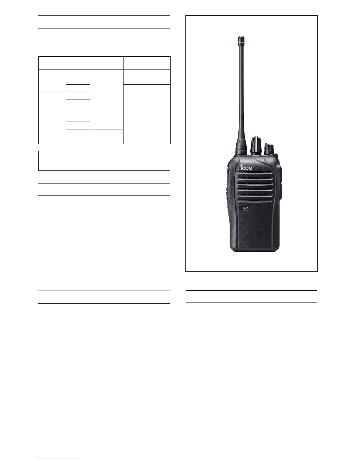
This service manual describes the latest technical
information for the IC-F4101D, IC-F4102D, IC-F4103D and
IC-F4106D
UHF TRANSCEIVERS, at the time of publication.
NEVER connect the transceiver to an AC outlet or to a DC
power supply that uses more than the specified voltage.
This will ruin the transceiver.
DO NOT expose the transceiver to rain, snow or any liquids.
DO NOT reverse the polarities of the power supply when
connecting the transceiver.
DO NOT apply an RF signal of more than 20 dBm (100 mW) to
the antenna connector. This could damage the transceiver’s
front-end.
To upgrade quality, any electrical or mechanical parts
and internal circuits are subject to change without notice
or obligation.
MODEL VERSION
FREQUENCY
RANGE (MHz)
CHANNEL
SPACING (kHz)
IC-F4101D USA-01
400–470
6.25/12.5
IC-F4102D
EUR-01 6.25/12.5/20.0/25.0
UK-01
6.25/12.5/25.0IC-F4103D
EXP-01
EXP-02
EXP-03
EXP-07
350–400
EXP-08
AUS-01
400–470
IC-F4106D RUS-01
Be sure to include the following four points when ordering
replacement parts:
1. 10-digit Icom part number
2. Component name
3. Equipment model name and unit name
4. Quantity required
<ORDER EXAMPLE>
1110003491 S.IC TA31136FNG IC-F4101D MAIN UNIT 5 pieces
8820001210 Screw 2438 screw IC-F4101D Top cover 10 pieces
Addresses are provided on the inside back cover for your
convenience.
ORDERING PARTS
1. Make sure that the problem is internal before disassembling the transceiver.
2. DO NOT open the transceiver until the transceiver is
disconnected from its power source.
3. DO NOT force any of the variable components. Turn them
slowly and smoothly.
4. DO NOT short any circuits or electronic parts. An
insulated tuning tool MUST be used for all adjustments.
5. DO NOT keep power ON for a long time when the
transceiver is defective.
6. DO NOT transmit power into a Standard Signal Generator
or a Sweep Generator.
7. ALWAYS connect a 30 dB to 40 dB attenuator between
the transceiver and a Deviation Meter or Spectrum
Analyzer, when using such test equipment.
8. READ the instructions of the test equipment throughly
before connecting it to the transceiver.
REPAIR NOTES
INTRODUCTION
CAUTION
Icom, Icom Inc. and the Icom logo are registered trademarks of Icom Incorporated (Japan) in Japan, the United States, the
United Kingdom, Germany, France, Spain, Russia and/or other countries.
Page 3

TABLE OF CONTENTS
SECTION 1 SPECIFICATIONS
SECTION 2 INSIDE VIEWS
SECTION 3 DISASSEMBLY INSTRUCTION
SECTION 4 CIRCUIT DESCRIPITON
4-1 RECEIVER CIRCUITS. . . . . . . . . . . . . . . . . . . . . . . . . . . . . . . . . . . . . . . . . . . . . . . . . . . . . . . . 4-1
4-2 TRANSMITTER CIRCUITS . . . . . . . . . . . . . . . . . . . . . . . . . . . . . . . . . . . . . . . . . . . . . . . . . . . . 4-2
4-3 FREQUENCY SYNTHESIZER CIRCUITS . . . . . . . . . . . . . . . . . . . . . . . . . . . . . . . . . . . . . . . . 4-3
4-4 VOLTAGE DIAGRAMS. . . . . . . . . . . . . . . . . . . . . . . . . . . . . . . . . . . . . . . . . . . . . . . . . . . . . . . . 4-3
4-5 PORT ALLOCATIONS . . . . . . . . . . . . . . . . . . . . . . . . . . . . . . . . . . . . . . . . . . . . . . . . . . . . . . . . 4-4
SECTION 5 ADJUSTMENT PROCEDURES
5-1 PREPARATION . . . . . . . . . . . . . . . . . . . . . . . . . . . . . . . . . . . . . . . . . . . . . . . . . . . . . . . . . . . . . 5-1
5-2 FREQUENCY ADJUSTMENT . . . . . . . . . . . . . . . . . . . . . . . . . . . . . . . . . . . . . . . . . . . . . . . . . . 5-4
5-3 TRANSMIT ADJUSTMENT . . . . . . . . . . . . . . . . . . . . . . . . . . . . . . . . . . . . . . . . . . . . . . . . . . . . 5-5
5-4 RECEIVE ADJUSTMENT . . . . . . . . . . . . . . . . . . . . . . . . . . . . . . . . . . . . . . . . . . . . . . . . . . . . . 5-7
SECTION 6 PARTS LIST
SECTION 7 MECHANICAL PARTS
SECTION 8 BOARD LAYOUTS
SECTION 9 BLOCK DIAGRAM
SECTION 10 VOLTAGE DIAGRAM
Page 4

1 - 1
SECTION 1. SPECIFICATIONS
M GENERAL
• Frequency range : 400–470 MHz [USA-01], [EUR-01], [UK-01], [EXP-01], [EXP-02], [EXP-03],
[AUS-01], [RUS-01]
350–400 MHz [EXP-07], [EXP-08]
• Number of conventional channels : 16
• Type of emission : Wide 16K0F3E (30.0 kHz) Except [USA], [EUR], [UK]
16K0F3E (25.0 KHz) Except [USA]
Middle 14K0F3E (20.0 kHz) [EUR], [UK] only
Narrow 11K0F3E (15.0 kHz) Except [EUR], [UK]
8K50F3E (12.5 kHz)
Digital 4K00F1E, D (6.25 kHz)
• Antenna impedance : 50 Ω (nominal)
• Operating temperature range : –30˚C to +60˚C; –22˚F to +140˚F Except [EUR], [UK]
–25˚C to +55˚C [EUR], [UK]
• Power supply voltage : Specifi ed Icom's battery packs only (7.5 V DC; negative ground)
• Current drain (approximately) : Receiving 100 mA (in digital mode, stand-by)
400 mA (max. audio, with the internal speaker)
Transmitting 1.3 A (4 W)
• Dimensions
(projections not included)
: 58.0 (W)×111.0 (H)×36.5 (D) mm; 2.3 (W)×4.4 (H)×1.4 (D) in. (with BP-265)
• Weight (approximately) : 150 g; 5.3 oz.
310 g; 10.9 oz. (including MB-124, BP-265, FA-SC57U)
M TRANSMITTER
• Output power : 4 W
• Modulation : Variable reactance frequency modulation
• Maximum frequency deviation : Narrow ±2.5 kHz
Middle ±4.0 kHz [EUR], [UK] only
Wide ±5.0 kHz Except [USA]
• Frequency stability : ±1.0 ppm
• Spurious emissions : 70 dB min. Except [EUR], [UK]
0.25 µW (
≤
1 GHz)
[EUR], [UK]
1.00 µW (
>
1 GHz)
[EUR], [UK]
• Adjacent channel power : Narrow 60 dB min., 70 dB typ.
Middle 70 dB min., [EUR], [UK] only
Wide 70 dB min., 74 dB typ. Except [USA]
Digital 60 dB min., 66 dB typ.
• Audio harmonic distortion : 1.0% typ. (at AF 1 kHz, 40% deviation)
• FSK error : 5% max.
• FM hum and Noise (Except [EUR], [UK])
(without CCITT Filter)
: Narrow 34 dB min., 44 dB typ.
Wide 40 dB min., 50 dB typ. Except [USA]
• Rasidual modulation ([EUR], [UK] only)
(with CCITT Filter)
: Narrow 40 dB min.
Middle 43 dB min.
Wide 45 dB min.
• Limitting charact of modulator : 60–100% of max. deviation
• Input impedance (MIC) : 2.2 k
Ω
Page 5

1 - 2
M RECEIVER
• Sensitivity : 0.24 µV typ. at 12 dB SINAD Except [EUR], [UK]
–4 dBµV (EMF) typ. at 20 dB SINAD [EUR], [UK]
–8 dBµV (EMF) typ. at 5% BER [Digital mode]
• Squelch sensitivity (at threshold) : 0.20 µV typ. Except [EUR], [UK]
–8 dBµV (EMF) typ. [EUR], [UK]
• Intermediate frequency : 1st IF; 46.35 MHz, 2nd IF; 450 kHz
• Adjacent channel selectivity : Narrow 60 dB min., 67 dB typ.
Middle 70 dB min. [EUR], [UK] only
Wide 70 dB min., 74 dB typ. Except [USA]
Digital 50 dB min., 58 dB typ.
• Spurious response : 70 dB min., 80 dB typ.
• Intermodulation : Narrow 70 dB min., 75 dB typ. Except [EUR], [UK]
Wide 70 dB min., 75 dB typ. Except [EUR], [UK], [USA]
Digital 65 dB min., 70 dB typ. Except [EUR], [UK]
65 dB min. [EUR], [UK]
• FM hum and Noise (Except [EUR], [UK])
(without CCITT Filter)
: Narrow 34 dB min., 42 dB typ.
Wide 40 dB min., 47 dB typ. Except [USA]
• FM hum and Noise ([EUR], [UK])
(with CCITT Filter)
: Narrow 40 dB min.
Middle 43 dB min.
Wide 45 dB min.
• Audio output power : 0.8 W typ. at 5% distorsion with a12 Ω load (internal speaker)
0.4 W typ. at 5% distorsion With an 8 Ω (external speaker)
• Audio output impedance : 8
Ω
Measurements made in accordance with TIA-603, EN 300 086 or EN 301 166.
All stated specifi cations are subject to change without notice or obligation.
Page 6
2 - 1
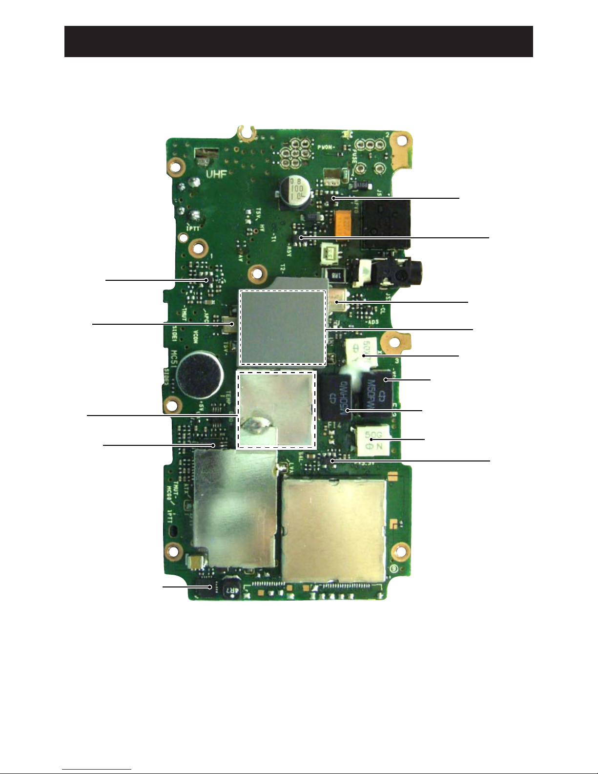
SECTION 2. INSIDE VIEWS
• MAIN-A/MAIN-C UNIT
(TOP VIEW)
VCO
5 V REGULATOR
(IC54)
PLL CIRCUIT
APC AMP
(IC1)
TCXO
(X2)
3.3 V DC-DC CONVERTER
(IC65)
MIC AMP
(IC64)
2ND IF FILTER (For wide)
(FI3)
1ST IF FILTER
(FI2)
DISCRIMINATOR
(X1)
2ND IF FILTER (For narrow)
(FI4)
2ND IF FILTER (For digital)
(FI5)
AF AMP
(IC21)
AF AMP
(IC58)
Page 7
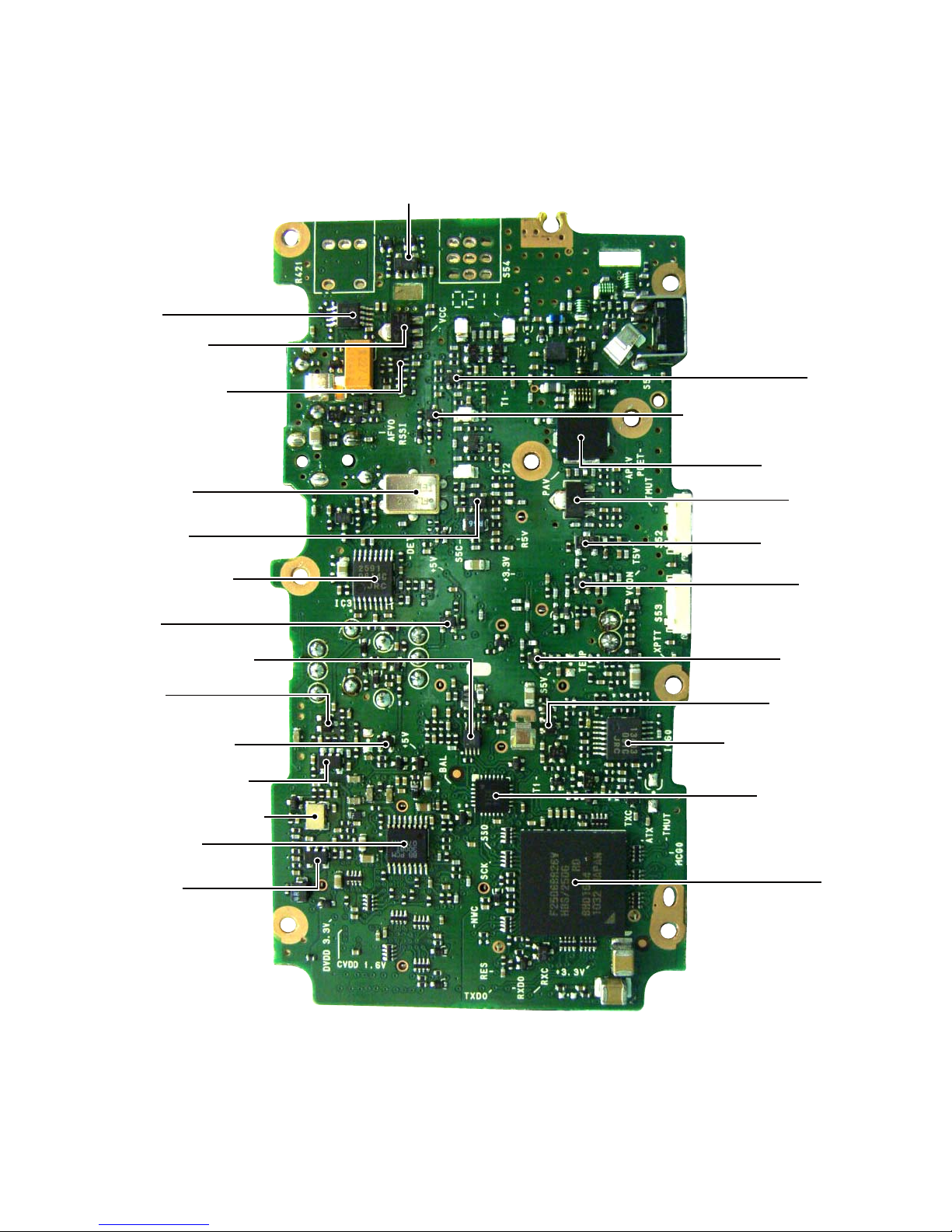
2 - 2
• MAIN-A/MAIN-C UNIT
(BOTTOM VIEW)
TX POWER AMP
(Q1)
BUFFER
(Q28)
PLL LOCK VOLTAGE SW
(IC6)
CLOCK AMP
(IC905)
2ND IF AMP (For digital)
(IC5)
AF POWER AMP SW
(Q64)
DRIVE AMP
(Q2)
PRE-DRIVE AMP
(Q3)
PRE AMP
(Q4)
RF AMP
(Q22)
RF AMP GATE BIAS CONTROL
(Q21)
AF AMP
(IC55)
IF DEMODULATOR IC
(IC3)
BUFFER
(Q17)
1ST IF FILTER
(FI1)
R5 LINE REGULATOR
(Q72)
RIPPLE FILTER
(Q15)
1ST IF MIXER
(Q23)
AF POWER AMP
CONTROLLER
(Q63)
LINEAR CODEC
(IC902)
LINEAR CODEC/DSP CLOCK
(X900)
D/A CONVERTER
(IC57)
LPF/BUFFER/VOX AMP
(IC60)
CPU
(IC51)
PLL BUFFER
(Q9)
VCC LINE SW
(Q92)
Page 8

3 - 1
SECTION 3. DISASSEMBLY INSTRUCTION
3 - 1
BE CAREFUL to not pull out the speaker wire when
separating the CHASSIS and the FRONT PANEL.
For easy separation of the CHASSIS
Use a suction lifter to lift the bottom of the CHASSIS up.
1. REMOVING THE CHASSIS
1) Remove the ANT connector nut and 2 knobs.
2. REMOVING THE MAIN UNIT
1) Remove the 9 screws and the side plate from the
MAIN UNIT.
2) Unsolder the 2 points shown, and then remove the
MAIN UNIT.
2) Remove 2 screws from the bottom of the CHASSIS.
3) Lift the bottom of the CHASSIS up in the direction
of the arrow.
4)
CAREFULLY lift the chassis out of the FRONT PANEL
and turn it over in order to unplug the speaker wire.
(Continued on the right above)
5) Remove the seals and nuts from the CHASSIS.
ANT CONNECTOR NUT
KNOB
FRONT PANEL
Remove with;
“ICOM Driver (K)”
(8960000110)
FRONT PANEL
CHASSIS
SCREW×2
SPEAKER
WIRE
CHASSIS
FRONT PANEL
TOP SEAL
NUT×2
SIDE SEAL
CHASSIS
Remove with;
“ICOM Driver (AG)”
(8960000560)
UNSOLDER
Solder
remover
CHASSIS
SCREW×9
PCB
MAIN UNIT
SIDE PLATE
Suction lifter
Suction lifter
• Part name : EA950R-2
• Manufacture : ESCO CO.LTD
Page 9
4 - 1
SECTION 4. CIRCUIT DESCRIPTION
4-1 RECEIVER CIRCUITS
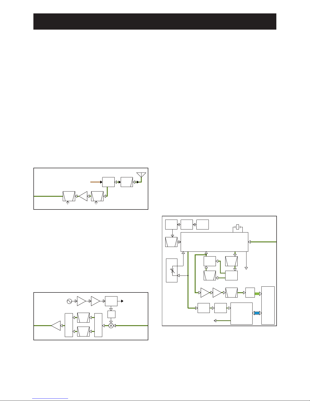
RF CIRCUITS
The RX signal from the antenna is passed through the LPF
and antenna SW (D3, D22), then filtered by the 2-staged
tuned BPF (D24 and D26) to eliminate unwanted out-ofband signals. The filtered RX signal is amplified by the RF
AMP (Q22), and filtered by another 2-staged tuned BPF
(D28) to obtain a good image response, then applied to the
1st IF circuits.
The BPFs are tuned to the RX frequency by applying adequate tuning voltages: “T1” and “T2” to the variable capacitors.
1ST IF CIRCUITS
The RX signal from the RF circuits is applied to the 1st IF
mixer (Q23) and mixed with the 1st LO signal from the RX
VCO, resulting in the 46.35 MHz 1st IF signal. The 1st IF signal is passed through the IF SWs (D31–D34) and the crystal
fi lter (FI1: analog mode, FI2: digital mode) to be fi ltered, amplified by the 1st IF AMP (Q24), then applied to the 2nd IF
circuits.
2ND IF AND DEMODULATOR CIRCUITS
The signal from the 1st IF circuits is applied to the IF demodulator IC (IC3) which contains the 2nd IF mixer, 2nd IF AMP,
FM detector, squelch circuit and AF AMP in its package.
The 1st IF signal is applied to the 2nd IF mixer and mixed
with the 2nd LO signal resulting in the 450 kHz 2nd IF signal.
The 2nd LO signal is generated by tripling the 15.3 MHz
reference frequency signal generated by the reference frequency oscillator (TCXO; X2).
• WHILE OPERATING IN THE ANALOG MODE
The 2nd IF signal is filtered by the 2nd IF filter (FI3: wide/
middle mode) or fi lters (FI3 and FI4: narrow) to eliminate unwanted signals. It is amplifi ed by the 2nd IF AMP, and then
demodulated by the detector circuit, which employs the discriminator (X1) as the phase shifter.
The demodulated AF signal is amplified by the AF AMP
(IC21), and then applied to the linear codec (IC902) through
the fi lter SW (Q901). The fi lter SW toggles the frequency response of the AF fi lter (R904, R908, C924), according to the
type of reception; Wide, Mid or Narrow.
The AF signal is converted into a digital audio signal by the
linear codec (IC902), processed by the DSP (IC903), and
then decoded into an analog audio signal.
• WHILE OPERATING IN THE DIGITAL MODE
The 2nd IF signal is fi ltered by the 2nd IF fi lters (FI3 and FI4)
to eliminate unwanted signals and applied to the IF AMP
(IC5) through the buffer (Q28). The amplifi ed 2nd IF signal is
passed through the ceramic fi lter (FI5), and then directly applied to the DSP (IC903).
The 2nd IF signal is demodulated by the DSP (IC903), and
then applied to the linear codec (IC902) to be decoded into
an analog audio signal.
The AF signal is applied to the RX AF circuits.
LPF
ANT
SW
D1,D22
RF
AMP
Q22
BPF
D28 D24,D26
BPF
T2
T1
From the TX circuits
To the 1st IF circuits
ANT
LO
SW
D5,D6
D31,D32D33,D34
Q23
BPF
XTAL
FI1
IF
AMP
Q24
BUFF
Q8
BUFF
Q10
ATT
IF SW
IF SW
RX VCO
To the TX circuits
From the RF circuits
2nd IF circuits
46.35MHz
BPF
XTAL
FI2
46.35MHz
1st IF mixer
PLL
IC
IC2
X3
Q26
BPF
X2
TCXO
W/N
SW
D38,D39
X1
Discriminator
BPF
CERAMIC
FI3
BPF
CERAMIC
FI4
W/N
SW
D36,D37
D/A
converter
IF IC
From the 1st IF
circuits
(Analog path)
To the RX AF circuit
(Digitalpath)
IC3
15.3MHz
45.9MHz
DISC
SQIN
IC57
450kHz
450kHz
NOIS
CERAMIC
BPF
FI5
DIF
BUFF
IC5
BUFF
Q28
A/D
IC901
FILTER
SW
Q901
DSP
LINEAR
DISC
CODEC
IC902
IC903
DAFO
AF
FILTER
R904,R908,C924
• 1ST IF CIRCUITS
• 2ND IF AND DEMODULATOR CIRCUITS
• RF CIRCUITS
Page 10
4 - 2
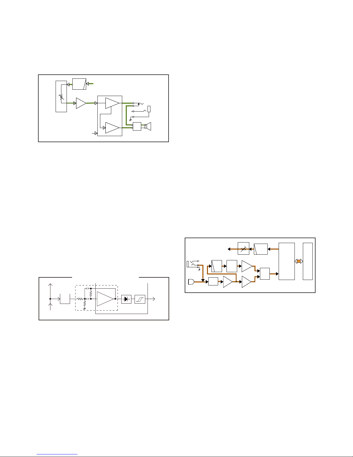
RX AF CIRCUITS
The demodulated AF signal from the linear codec (IC902) is
passed through the LPF (IC60C), and then adjusted in level
by the D/A converter (IC57). The level-adjusted AF signal is
then amplifi ed by AF AMPs (IC58 and IC55).
The amplifi ed AF signal is applied to the internal or external
speaker.
SQUELCH CIRCUITS (Analog mode only)
The squelch circuit cuts off the AF output signals when no
RF signals are received. Detecting noise components in the
demodulated AF signals, the squelch circuit stops audio signals being emitted.
A portion of demodulated AF signal from the IF IC (IC3) is
passed through the D/A converter (IC57) for level (=threshold) adjustment. The level-adjusted AF signals are passed
through the noise filter (IC3, pins 7, 8 and R139–R142,
C241–C243) to fi lter the noise components (approx. 30 kHz
signals) only. The noise components are rectified, resulting
in DC voltage corresponding to the noise level.
If the noise level is higher than the preset one, the internal
comparator set the “NOISE” signal to the CPU to “High”,
then the CPU turns the “AFON” signal which controlls the AF
power AMP (IC55) to “Low,” to inactivate it.
• RX AF CIRCUITS
• SQUELCH CIRCUITS
AF
AM P
AF
AMP
IC55 TPA0211DGN
J52
SP1
AF
AM P
J53
Int.speaker
Ext.speaker
1
2
LPF
IC60C
From the linear codec
IC58
AFON
AFO
DAFO
D/A
converter
IC57
DAC
Noise
AMP
Noise filter
From IF IC
(IC3, Pin16)
To RX AF circuits
Noise
detector
Com-
parator
NOISE SQUELCH DIAGRAM
“NOIS”
IC57
IC3
14
8
7
13
15
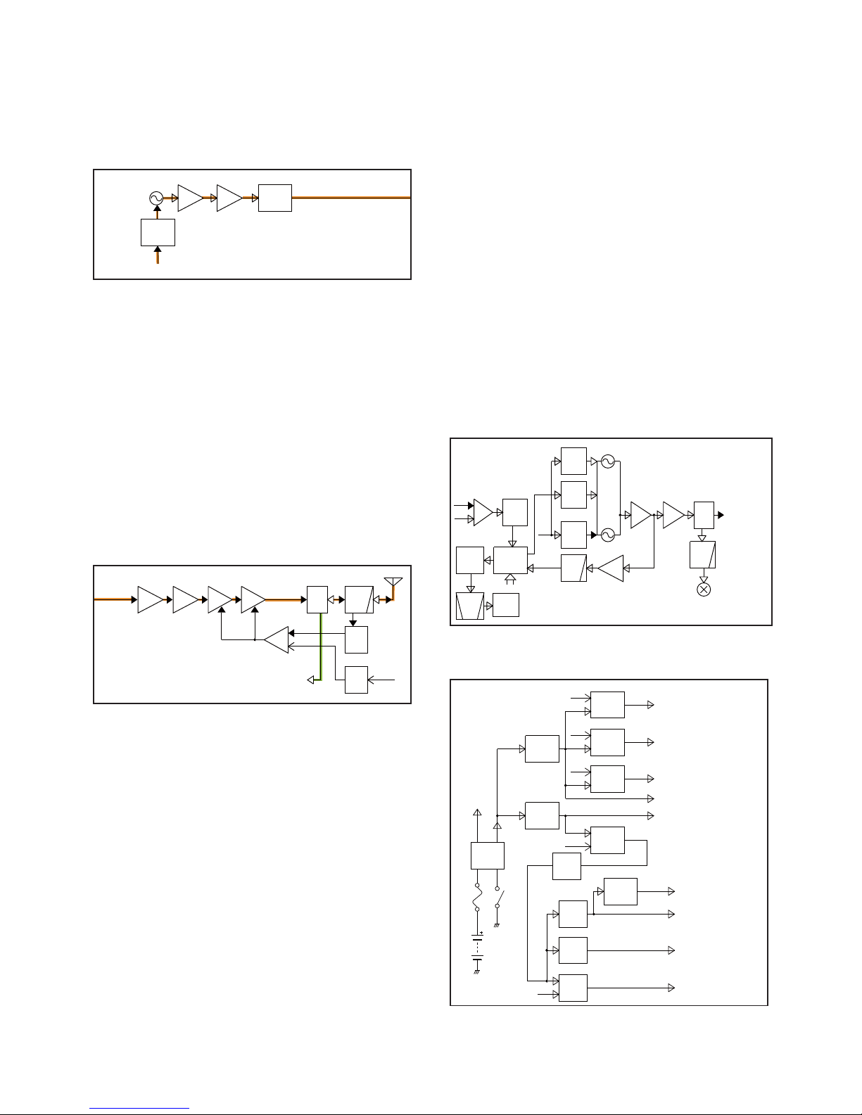
4-2 TRANSMITTER CIRCUITS
TX AF CIRCUITS
The audio signal from the internal or external microphone
(MIC signal) is passed through the MIC gain SW (IC62), and
then applied to the MIC AMP (IC64).
• WHILE OPERATING IN THE ANALOG MODE
The amplifi ed MIC signal is passed through the HPF (IC63A),
which attenuates frequencies 300 Hz and below, and then
applied to the limiter AMP (IC60A), through the mute SW
(Q66).
The amplitude-limited MIC signal is applied to the lin-
ear codec (IC902), through the MIC line SW (IC66).
The MIC signal is converted into a digital audio signal by the
linear codec (IC902), processed by the DSP (IC903), and
then converted into an analog baseband signal (modulation
signal).
• WHILE OPERATING IN THE DIGITAL MODE
The amplifi ed MIC signal is applied to the ALC (IC63B) which
keeps the signal level fi xed.
The level-adjusted MIC signal is
applied to the linear codec
(IC902) through the MIC line SW (IC66).
The MIC signal is converted into a digital audio signal by the
linear codec (IC902), processed by the DSP (IC903), and
then converted into the digital baseband signal (modulation
signal).
The signal from the linear codec (IC902) is passed through
the LPF (IC60B), and then applied to the D/A converter
(IC57)
which adjusts its level (=deviation)
. The level-adjusted
modulation signal is applied to the modulation circuit.
• TX AF CIRCUITS
MC51
[Ext. MIC]
[Int. MIC]
J51
MIC
GAIN
SW
IC62
AMP
IC64
ALC
AMP
IC63B
HPF
IC63A
LIMIT
AMP
IC60A
MIC
LINE
IC66
SW
MUTE
SW
Q66
DMI
To the modulation circuit
DSP
LINEAR
CODEC
IC902
IC903
LPF
IC60B
MOD DMO
D/A
IC57
Page 11
4 - 3
MODULATION CIRCUIT
The modulation signal from the TX AF circuits is applied to
D15 of the TX VCO (Q14, D14–D16) to modulate it (FM for
the analog mode, 4FSK for the digital mode). The modulated
signal from the TX VCO is buffer-amplified by two buffers
(Q8, Q10), and applied to the TX AMP circuits through the
LO SW (D5).
TX AMPLIFIERS
The buffer amplifi ed signal from the LO SW (D5) is sequentially amplified by the pre-AMP (Q4), pre-drive AMP (Q3),
drive AMP (Q2), and power AMP (Q1), to obtain TX power.
The amplifi ed TX signal is passed through the antenna SW
(D3, D22) and the LPF, which eliminates harmonics, and
then fed to the antenna.
APC CIRCUITS
D1 and D2 rectify a portion of the TX signal to direct voltage,
and the APC AMP (IC1) compares the voltage and the TX
power control reference voltage, “T1.” The resulting voltage
controls the gain of the power and drive AMPs to keep the
TX power constant.
• FREQUENCY SYNTHESIZER CIRCUITS
• TX AMPLIFIERS AND APC CIRCUITS
5-4 VOLTAGE DIAGRAMS
LO
SW
D5
Q14,
D14,D16,D17
MODULATION
FM:Analog
4-FSK: Digital
D15
BUFF
Q8
BUFF
Q10
TX VCO
From the TX AF circuits
To the TX AMP circuits
MOD
LPF
PWR
DET
D1,D2
MUTE
SW
Q6
ANT
SW
D1,D22
PWR
AMP
Q1
APC
AMP
IC1
DRIVE
AMP
Q2
AMP
PRE
Q4
DRIVE
PRE
Q3
T1
TMUT
ANT
From the
TX VCO
To the RX circuits
• MODULATION CIRCUIT
LPF
LPF
LO
SW
D5,D6
Q13,D12
Q14,D16
FILTER
LOOP
PLL
IC
SO,SCL,PLST
IC4
X3
Q26
Q23
To the TX AMPs
BPF
BUFF
Q8
BUFF
Q10
BUFF
Q9
X2
TCXO
LV
ADJ
D14
LV
ADJ
D11
BUFF
IC60
IF IC
RX VCO
TX VCO
IC3
REF
BAL
15.3MHz
45.9MHz
1st IF mixer
LV
LVA
S5
REG
Q71
,Q86
REG
R5
Q72
,Q87
REG
T5
Q73
,Q88
F51
R1(CHASSIS)
12
BT1
REG
+5V
IC54
DC-DC
1.6V
IC900
DC-DC
3.3V
IC65
REG
+3.3V
Q90
,Q91
Q92,
Q93,
D59
POWER
SW
LINE
FILTER
LINE
FILTER
LINE
FILTER
LINE
FILTER
VCC
+5V
T5V
Transmit circuits
Receive circuits
TX/RX common circuits
TX/RX common circuits
Logic circuits
R5V
S5V
TXC
RXC
S5C
VCC CPUV
CVDD_1.6 V
3.3V_VD D
+3.3V
+3.3V_A
+3.3V
PWON
POSWH
DVDD_3.3V
DSP
DSP flash
Liner codec
DSP reference voltage
CPUV
4-3
FREQUENCY SYNTHESIZER CIRCUITS
The RX VCO is composed of Q13, and D11, D12. The VCO
output signal is buffer-amplifi ed by two buffers (Q8 and Q10)
and applied to the 1st IF mixer, through the LO SW (D6) and
the LPF (L18, C208, C209).
The TX VCO is composed of Q14 and D14–D17. The VCO
output signal is buffer-amplifi ed by two buffers (Q8 and Q10)
and applied to the pre-AMP (Q4), through the LO SW (D5)
and the LPF.
A portion of signal generated by each VCO is fed back to
the PLL IC (IC4, pin 17) through the buffer (Q9) and the LPF
(L46, C167, C168).
The applied VCO output signal is divided and phase-compared with a 15.3 MHz reference frequency signal from the
TCXO (X2), which is also divided. The resulting signal is
output from the PLL IC (IC4), and DC-converted by the loop
fi lter, and then applied to the VCO as the lock voltage.
When the oscillation frequency drifts, its phase changes
from that of the reference frequency, causing a lock voltage
change to compensate for the drift in the VCO oscillating frequency.
Page 12
4 - 4
4-5 PORT ALLOCATIONS
• CPU (IC51)
• D/A CONVERTER (IC57)
PIN
No.
LINE
NAME
DESCRIPTION
3 BAL DTCS balance adjustment.
4 AFVO AF volume adjustment.
12 TENC Outputs CTCSS deviation adjustment.
15 SQLC Squelch threshold setting.
16 T1
During RX: Outputs BPF tuning voltage.
During TX: Outputs TX power reference
voltage.
19 T2 Outputs BPF tuning voltage.
20 REF Outputs reference frequency adjust voltage.
23 LVA Outputs additional lock voltage adjustment.
24 MOD Max. deviation/AF volume adjustment.
BALL
No.
LINE
NAME
DESCRIPTION
I/O
A5 RXC
Power supply switching control.
H= During receive or stand-by.
O
A6 RMUTE
RX AF mute switch control.
L= During the squelch circuit is
activated.
O
A7 DMOSI Serial data to the DSP (IC903). O
A15 PWON
Power supply switching control.
H= The transceiver's power is ON.
O
B12 NOIS
Noise level detect.
H= Squelch close.
I
B15 AFON
AF power AMP control.
H= AF power AMP (IC55) is activated.
O
C1, C2CBI2,
CBI0
[ROTARY SELECTOR] input. I
C5 TXC
Power supply switching control.
H= While transmitting.
O
C8 ESDA EEPROM (IC52) serial data. I/O
C13 POSW [POWER] input. I
C14 ADS
1st IF filters (FI1 and FI2) switching
control.
L= During digital mode.
O
C15 NWC
Receive bandwidth switching.
L= During narrow mode.
O
D2, D3CBI3,
CBI1
[ROTARY SELECTOR] input. I
D6 DSCK DSP (IC903) clock. O
D8 ESCL EEPROM (IC52) clock. O
D13 DPDN
DSP (IC903) power control.
H= DSP is inactivated.
O
D14 DRES
DSP (IC903) reset.
L= Reset.
O
D15 CSFT
Clock frequency shift.
H= Clock frequency is shifted.
O
E13 RES CPU reset. I
H1 SIDE1
[UPPER] key input.
L= Pushed.
I
H2 SIDE2
[LOWER] key input.
L= Pushed.
I
J1 IPTT
Internal [PTT] input.
L= Pushed.
I
J2 XPTT
External PTT input.
H= An external PTT is pushed.
I
L1, L2
MCG0,
MCG1
MIC gain control. O
L12 TLED
Busy LED (Red) control.
L= LED lights
. (While transmitting)
O
L13 RLED
Busy LED (Green) control.
L= LED lights. (While receiving a signal)
O
L14 SSO Common serial data. O
L15 SCK Common clock. O
M1 TMUT
Transmission mute.
L= TX inhibit.
O
M2 ATX
Automatic TX control for VOX mode.
H= While MIC audio from the
connected headset is detected.
O
M8 BEEP Beep audio. (Square waves) O
M11 MDET External connection detect. I
M14 DAST
D/A converter (IC57) strobe.
H= Load enable.
O
BALL
No.
LINE
NAME
DESCRIPTION
I/O
N11 VOXV Microphone input sensing voltage. I
N12 BATV Battery voltage sensing. I
N14 DMISO DSP (IC903) serial data. O
P4 PLSW
PLL lock up time control.
L= Fast lock up.
O
P10 TEMP Temperature sensing voltage. I
P11 RSSI RSSI sensing voltage. I
P12 AFVI [VOLUME CONTROL] input. I
P15 DSS DSP (IC903) chip select. O
R3 S5C
Power supply line "S5C" switching
control.
H= Supplying current to the TX/RX
common circuits.
O
R4 PLST PLL strobe. O
R10 LVIN Lock voltage input. I
Page 13

5 - 1
SECTION 5. ADJUSTMENT PROCEDURE
¤ JIG CABLE
EQUIPMENT GRADE AND RANGE EQUIPMENT GRADE AND RANGE
Cloning software CS-F3100D/F5120D
(Revision 1.0 or later)
JIG cable
Modifi ed OPC-478UC (See the illust below)
RF power meter
(50 Ω terminated)
Measuring range : 0.1–10 W
Frequency range : 100–600 MHz
SWR : Less than 1.2 : 1
Frequency counter
Frequency range : 0.1–600 MHz
Frequency accuracy : ±1 ppm or better
Input level : Less than 1 mW
Modulation
Analyzer
Frequency range : 30–600 MHz
Measuring range : 0 to ±10 kHz
Standard signal
generator (SSG)
Frequency range : 0.1–600 MHz
Output level : –20 dBµ to 90 dBµ
(–127 to –17 dBm)
AC millivoltmeter Measuring range : 10 mV to 10 V
Oscilloscope
Frequency range : DC–20 MHz
Measuring range : 0.01–20 V
Attenuator
Power attenuation : 30 dB
Capacity : More than 10 W
Audio generator
(AG)
Frequency range : 300–3000 Hz
Output level : 1–500 mV
External speaker
Input impedance : 8
Ω
Capacity : More than 1 W
¤ REQUIRED EQUIPMENTS
5-1 PREPARATION
3-conductor 2.5 (d) mm plug
(MIC)
(GND
)
33 k
3-conductor 3.5(d) mm plug
(CLONE)
OPC-478UC
(GND)
(SP)
[JIG cable1]
[JIG cable2]
+−
AC
MILLIVOLTMETER
(10 mV to 10 V)
AUDIO GENERATOR
(300–3000 Hz/1–500 mV)
+−
PTT
+
4.7 µF
EXT. SPEAKER
(1 W/8 Ω)
+
−
SETTING;
Frequency : 1 kHz
Level : 150 mV
Waveform : Sine wave
¤ CONNECTION
Modulation
analyzer
Speaker (8 Ω)
to the antenna connector
Attenuator
30 dB
RF power meter
0.1– 10 W/50 Ω
Frequency
counter
Standard signal generator
–20 to 90 dBµ
(–127 to –17 dBm)
CAUTION!
NEVER transmit while
an SSG is connected to
the antenna connector.
To [SP]
To [MIC]
(JIG cable 1)
(JIG cable 2)
To [SP] connector
PC
to USB port
OPC-478UC
(USB type)
Page 14

5 - 2
CONVENIENT: The cloning data fi le for the adjustment, as described in this service manual, is attached.
Right click the clip icon, and select "Save Embeded File to Disk."
• For 400 MHz band versions: • For 350 MHz band versions:
¤ ADJUSTMENT CHANNELS
• For 350 MHz band versions
• For 400 MHz band versions
Before starting the adjustments, use the cloning software to create the same cloning file as shown below, then
upload it into the transceiver.
Page 15

S-METER
DIGITAL DEVIATION
2/5 TONE DEVIATION
5 - 3
¤ ADJUSTMENT UTILITY
ADJUSTMENT CONDITION
REFERENCE FREQUENCY
TX OUTPUT POWER
FM DEVIATION
SQUELCH
SENSITIVITY
PLL LOCK VOLTAGE
CTCSS DEVIATION
DTCS DEVIATION
MODULATION BALANCE
For [EUR] versions:
When adjusting “Deviation” in the middle band, change the bandwidth
to “Middle” as shown.
Select “Middle”
Page 16
5 - 4
ADJUSTMENT
TRANSCEIVER’S
CONDITION
OPERATION
ADJUSTMENT
ITEM
VALUE
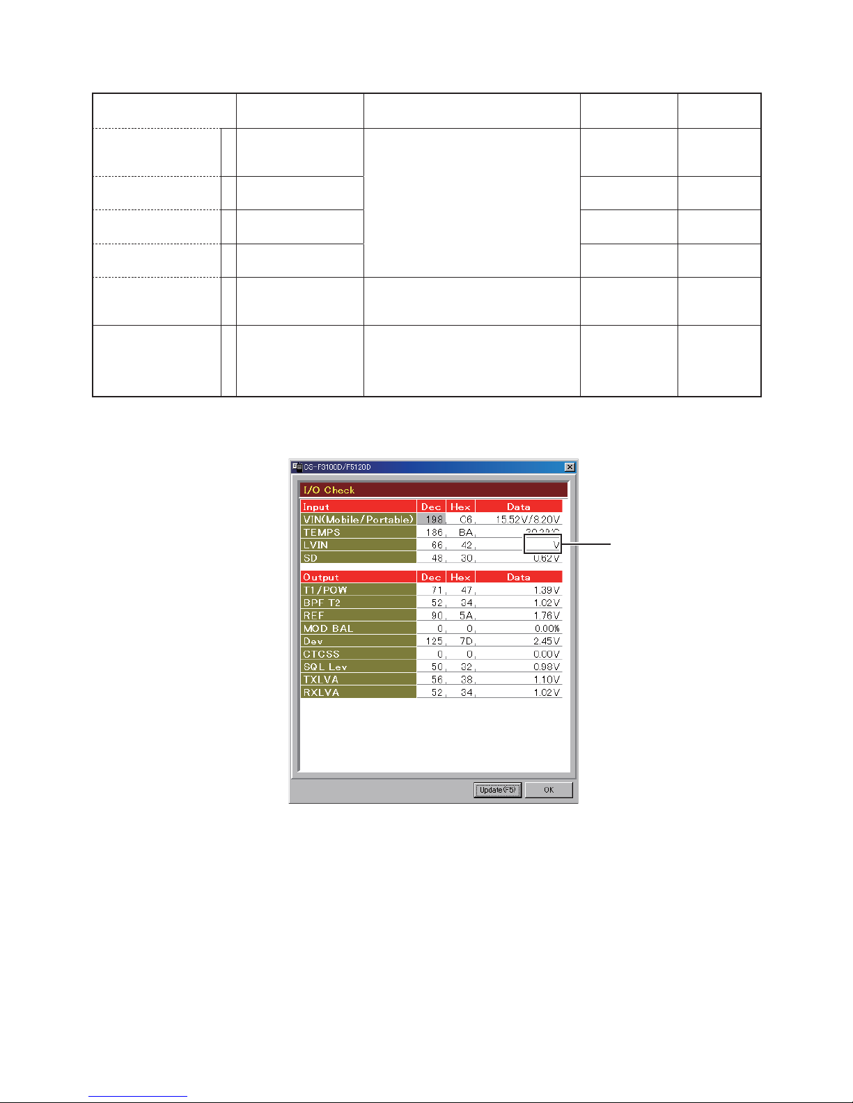
PLL LOCK VOLTAGE
-RX(Band low)
1 • Channel : 1-1
• Receiving
1) Connect an RF power meter to the
antenna connector.
2) Set the preset adjustment value on
the adjustment utility window.
[RX LVA(Adjust)]
1.00 V
(Band high) 2 • Channel : 1-2
• Receiving
[RX LVA(Check)] 3.70 V
-TX(Band low)
3 • Channel : 1-1
• Transmitting
[TX LVA(Adjust)]
1.00 V
(Band high)* 4 • Channel : 1-2
• Transmitting
[TX LVA(Check)]
3.20 V
-VERIFY-** 5 • Channel : 1-2
• Transmitting
• Click the [Update (F5)] button to check
on the "I/O Check window" as below.
[LVIN]
(On the "I/O
Check window")
2.00–4.00 V
(Verify)
REFERENCE
FREQUENCY
1 • Channel : 1-3
• Transmitting
• Loosely couple a frequency counter to
the antenna connector.
[REF]
470.000000 MHz
[400 MHz band]
400.000000 MHz
[350 MHz band]
(±50 Hz)
*: For only [350 MHz band]. **: For only [400 MHz band].
5-2 FREQUENCY ADJUSTMENTS
1) Select an adjustment item using [↑]/[↓] on the PC's keyboard.
2) Set or modify the adjustment value as specifi ed using [←]/[→] on the PC's keyboard, then push [ENTER].
• I/O Check window
(The values shown above are an example only. Each transceiver has own values.)
Lock voltage
appears here
* * *
Page 17

5 - 5
ADJUSTMENT
TRANSCEIVER’S
CONDITION
OPERATION
ADJUSTMENT
ITEM
VALUE
TX OUTPUT
POWER
(Hi power)
1 • Channel : 1-4
• Transmitting
• Connect an RF power meter to the antenna connector. [Power (Hi)]
4.0 W
(L2 power) 2 • Channel : 1-5
• Transmitting
[Power (L2)] 2.0 W
(L1 power) 3 • Channel : 1-6
• Transmitting
[Power (L1)]
1.0 W
MODULATION
BALANCE
1
–
• Set “MOD -Narrow-” to “90,” and set the
TX mode to “2” on the “ADJUSTMENT
UTILITY” screen.
[MOD -Narrow-] 90
[TX mode] 2
2• Set the coursor on [BAL Start] to enter the “MODULATION BAL-
ANCE” adjustment mode.
[BAL Start] –
(Band low) 3 • Channel : 1-7
• Transmitting
• Connect a modulation analyzer with an
oscilloscope to the antenna connector
through an attenuator, and set it as;
HPF : OFF
LPF : 15 kHz
De-emphasis : OFF
Detector : (P–P)/2
[BAL 1]
(Band center) 4 • Channel : 1-8
• Transmitting [BAL 2]
(Band high) 5 • Channel : 1-9
• Transmitting [BAL 3]
6• Set the coursor on [BAL Start] to quit the “MODULATION BAL-
ANCE” adjustment mode.
[BAL Start] –
FM DEVIATION
-Narrow(Band low)
1• Set the coursor on [MOD N Start] to enter the “FM DEVIATION
-Narrow-” adjustment mode.
[MOD N Start]
–
2 • Channel : 1-10
• Transmitting
• Connect a modulation analyzer to
the antenna connector through an
attenuator, and set it as “MODULATION
BALANCE.”
• Connect an audio generator to the [MIC]
jack through the JIG cable, and set it as;
Frequency : 1 kHz
Waveform : Sinewave
Level : 150 mVrms
[MOD N L]
±2.05 to ±2.15
kHz
(Band center) 3 • Channel : 1-11
• Transmitting
[MOD N C]
(Band high) 4 • Channel : 1-12
• Transmitting
[MOD N H]
5• Set the coursor on [MOD N Start] to quit the “FM DEVIATION
-Narrow-” adjustment mode.
[MOD N Start]
–
FM DEVIATION
-Wide-*
(Band low)
1• Set the coursor on [MOD W Start] to enter the “FM DEVIATION
-Wide-” adjustment mode.
[MOD W Start]
–
2 • Channel : 1-13
• Transmitting
• Connect a modulation analyzer to
the antenna connector through an
attenuator, and set it as “MODULATION
BALANCE.”
• Connect an audio generator to the [MIC]
jack through the JIG cable, and set it as
“FM DEVIATION -Wide-.”
[MOD W L]
±4.05 to ±4.15
kHz±
(Band center) 3
• Channel : 1-14
• Transmitting
[MOD W C]
(Band high) 4 • Channel : 1-15
• Transmitting
[MOD W H]
5• Set the coursor on [MOD W Start] to quit the “FM DEVIATION
-Wide-” adjustment mode.
[MOD W Start]
–
*: For all models except [USA].
5-3 TRANSMIT ADJUSTMENTS
1) Select an adjustment item using [↑]/[↓] on the PC's keyboard.
2) Set or modify the adjustment value as specifi ed using [←]/[→] on the PC's keyboard, then push [ENTER].
No over or under shoot.
As flat as possible.
Page 18

5 - 6
5-3 TRANSMIT ADJUSTMENTS (Continued)
1) Select an adjustment item using [↑]/[↓] on the PC's keyboard.
2) Set or modify the adjustment value as specifi ed using [←]/[→] on the PC's keyboard, then push [ENTER].
ADJUSTMENT
TRANSCEIVER’S
CONDITION
OPERATION
ADJUSTMENT
ITEM
VALUE
FM DEVIATION
-Middle-***
(Band low)
1• Set the coursor on [MOD W Start] to enter the “FM DEVIATION
-Middle-” adjustment mode.
[MOD M Start]
–
2 • Channel : 1-16
• Transmitting
• Connect a modulation analyzer with an
oscilloscope to the antenna connector
through an attenuator, and set it as;
HPF : OFF
LPF : 15 kHz
De-emphasis : OFF
Detector : (P–P)/2
• Connect an audio generator to the [MIC]
jack through the JIG cable, and set it as;
Frequency : 1 kHz
Waveform : Sine wave
Level : 150 mVrms
[MOD M L]
±3.25 to ±3.35
kHz±
(Band center) 3 • Channel : 1-17
• Transmitting
[MOD M C]
(Band high) 4 • Channel : 1-18
• Transmitting
[MOD M H]
5• Set the coursor on [MOD W Start] to quit the “FM DEVIATION
-Middle-” adjustment mode.
[MOD M Start]
–
DIGITAL
DEVIATION
(Band low)
1• Set the coursor on [MOD D Start] to enter the “DIGITAL DEVIA-
TION” adjustment mode.
[MOD N Start]
–
2 • Channel : 1-19
• Transmitting
• Connect a modulation analyzer to
the antenna connector through an
attenuator, and set it as “FM DEVIATION -Middle-.”
• Connect an audio generator to the [MIC]
jack through the JIG cable, and set it as
“FM DEVIATION -Middle-.”
[MOD D L]
±1.36 to ±1.40
kHz
(Band center) 3 • Channel : 1-20
• Transmitting
[MOD D C]
(Band high) 4 • Channel : 1-21
• Transmitting
[MOD D H]
5• Set the coursor on [MOD D Start] to quit the “DIGITAL DEVIA-
TION” adjustment mode.
[MOD N Start]
–
CTCSS
DEVIATION
1 • Channel : 1-22*
1-23**
• No AF input from
the MIC.
• Transmitting
• Connect a modulation analyzer with an
oscilloscope to the antenna connector
through an attenuator, and set it as;
HPF : OFF
LPF : 15 kHz
De-emphasis : OFF
Detector : (P–P)/2
[CTCSS]
±0.65 to ±0.75 kHz*
±0.30 to ±0.40 kHz**
DTCS DEVIATION 1 • Channel : 1-24*
1-25**
• No AF input from
the MIC.
• Transmitting
• Connect a modulation analyzer to
the antenna connector through an
attenuator, and set it as “CTCSS DEVIATION.”
[DTCS]
±0.65 to ±0.75 kHz*
±0.30 to ±0.40 kHz**
2/5 TONE, DTMF
DEVIATION
1 • Channel : 1-26
• Transmitting
• Set the TX mode to “5” on the “ADJUSTMENT UTILITY” screen.
[TX Mode]
5
2• Connect a modulation analyzer to
the antenna connector through an
attenuator, and set it as "MODULATION
BALANCE."
[S.Tone]
±1.45 to ±1.55
kHz
*: For all models except [USA]. **: For [USA] ***: For only [EUR].
Page 19

5 - 7
ADJUSTMENT
TRANSCEIVER’S
CONDITION
OPERATION
ADJUSTMENT
ITEM
VALUE
RECEIVE
SENSITIVITY
NOTE:
“RECEIVE SENSITIVITY” must be adjusted before “S-METER.” Otherwise, “S-METER” will not beadjusted
properly. When “RECEIVE SENSITIVITY” is re-adjusted, “S-METER” must be also re-adjusted.
1 • Channel : 1-27*
1-28**
• Receiving
• Connect an SSG to the antenna connector and set it as;
Frequency : 400 MHz [400 MHz band]
350 MHz [350 MHz band]
Level
†
: +20 dBµ (–87 dBm)
Modulation : 1 kHz
Deviation : ±3.0 kHz*
±1.5 kHz**
[BPF C ALL]
Push [ENTER]
(Automatic
adjustment)
S-METER NOTE: When “RECEIVE SENSITIVITY” is re-adjusted, “S-METER” must be also re-adjusted.
1 • Channel : 1-29*
1-30**
• Receiving
• Connect an SSG to the antenna connec-
tor and set it as;
Frequency : 400 MHz [400 MHz band]
350 MHz [350 MHz band]
Level
†
: +23 dBµ (–84 dBm)
Modulation : 1 kHz
Deviation : ±3.0 kHz*
±1.5 kHz**
[RSSI S3 Level]
Push [ENTER]
(Automatic
adjustment)
2• Set the SSG as;
Level
†
: –7 dBµ (–114 dBm)
[RSSI S1 Level]
SQUELCH NOTE: When “RECEIVE SENSITIVITY” is re-adjusted, “SQUELCH” must be also re-adjusted.
1 • Channel : 1-31*
1-32**
• Receiving
1) Connect an SSG to the antenna con-
nector and set it as;
Frequency : 400 MHz [400 MHz band]
350 MHz [350 MHz band]
Level
†
: –14 dBµ (–121 dBm)
Modulation : 1 kHz
Deviation : ±3.0 kHz*
±1.5 kHz**
2) Once close the squelch by increasing the
[SQL] value, and then decrease the value
to open the squelch.
[SQL]
Squelch opens
(Push [ENTER]
to store the
value
)
†
; The output level of the standard signal generator (SSG) is indicated as the SSG’s open circuit.
*: For all models except [USA]. **: For [USA]
5-4 RECEIVE ADJUSTMENTS
1) Select an adjustment item using [↑]/[↓] on the PC's keyboard.
2) Set or modify the adjustment value as specifi ed using [←]/[→] on the PC's keyboard, then push [ENTER].
Page 20

6 - 1
SECTION 6. PARTS LIST
IC1 1110002751 S.IC TA75S01F(TE85RF) T 32.5/8.9
IC3 1110007320 S.IC NJM2591V-TE1-#ZZZB B 45.8/38.9
IC4 1130015270 S.IC AK1541P-L T 43.2/24.0
IC5 1110006230 S.IC NJM2711F-TE1-#ZZZB B 68.3/44.2
IC6 1130011741 S.IC TC7W66FK(TE85LF) B 65.3/26.7
IC21 1110002751 S.IC TA75S01F(TE85RF) T 69.8/34.6
IC51 1140015010 S.IC HD64F2506RBR26DV(EMPTY) B 83.0/14.3
IC52 1130015080 S.IC R1EX24512ASAS0A T 83.6/16.4
IC53 1110007780 S.IC NJU7704F3-28A-TE1-#ZZZH T 85.0/11.3
IC54 1180003600 S.REG NJM2871BF05-TE1-#ZZZB T 15.5/34.8
IC55 1110007610 S.IC TPA0211DGNR B 13.3/42.1
IC57 1110007290 S.IC AK2330P-L B 72.3/24.3
IC58 1110002751 S.IC TA75S01F(TE85RF) T 23.9/28.3
IC60 1110005320 S.IC NJM13403V-TE1-#ZZZB B 65.1/8.3
IC62 1130011741 S.IC TC7W66FK(TE85LF) T 60.9/11.3
IC63 1110007630 S.IC NJM2783V-TE1-#ZZZH T 71.9/9.8
IC64 1110005330 S.IC NJM12904V-TE1-#ZZZB T 67.1/9.8
IC65 1180003670 S.REG BD9141MUV-E2 T 96.5/9.1
IC66 1130009981 S.IC TC7W53FK(TE85LF) T 75.9/8.5
IC900 1180003680 S.REG TPS62204DBVR T 76.4/39.0
IC901 1190002900 S.IC ADS7886SDCKR T 77.5/32.5
IC902 1110007770 S.IC PCM3008T/2K B 78.6/34.7
IC903 1140013290 S.IC TMS320VC5509AZHH T 86.8/36.8
IC904 1130015620 S.IC EN25Q40-100GIP <MSK> T 78.0/28.4
IC905 1110006230 S.IC NJM2711F-TE1-#ZZZB B 80.2/46.0
Q1 1560001700 S.FET RD07MUS2B-T112 B 28.6/13.5
Q2 1560001241 S.FET RD01MUS1-T113 B 36.1/14.4
Q3 1530004180 S.TRA 2SC3356-T1B YS (R25) B 41.3/12.9
Q4 1530003311 S.TRA 2SC5107-O(TE85RF) B 46.2/13.4
Q8 1530003311 S.TRA 2SC5107-O(TE85RF) T 55.6/18.6
Q9 1530003311 S.TRA 2SC5107-O(TE85RF) B 55.4/18.9
Q10 1530003311 S.TRA 2SC5107-O(TE85RF) T 61.0/19.4
Q11 1590004070 S.TRA LDTC144EET1G <SLVJ> B 53.4/23.2
Q12 1590004070 S.TRA LDTC144EET1G <SLVJ> B 62.7/23.3
Q13 1530002921 S.TRA 2SC4226-T1 Y25 (R25) T 56.5/22.6
Q14 1530002921 S.TRA 2SC4226-T1 Y25 (R25) T 62.2/22.3
Q15 1530002851 S.TRA 2SC4116-BL(TE85RF) B 63.6/17.2
Q16 1590004090 S.TRA LDTC114YET1G <SLVJ> B 68.5/21.3
Q17 1560000541 S.FET 2SK880-Y(T5RICOMF) B 50.9/29.7
Q21 1560000841 S.FET 2SK1829(TE85RF) B 25.7/31.5
Q22 1580000731 S.FET 3SK293(TE85LF) B 21.2/29.0
Q23 1580000731 S.FET 3SK293(TE85LF) B 36.4/26.1
Q24 1530003311 S.TRA 2SC5107-O(TE85RF) B 38.3/42.6
Q26 1530002851 S.TRA 2SC4116-BL(TE85RF) T 43.3/32.7
Q27 1590004090 S.TRA LDTC114YET1G <SLVJ> B 56.3/35.9
Q28 1530002851 S.TRA 2SC4116-BL(TE85RF) B 63.6/44.7
Q29 1590004090 S.TRA LDTC114YET1G <SLVJ> T 38.5/42.6
Q51 1510001090 S.TRA KTA2015Y-RTK/P B 25.7/43.5
Q52 1590004090 S.TRA LDTC114YET1G <SLVJ> B 24.6/39.8
Q58 1590004220 S.TRA DRA9123Y0L B 54.9/7.1
Q59 1590004090 S.TRA LDTC114YET1G <SLVJ> B 49.1/7.3
Q63 1520000460 S.TRA 2SB1132 T100 R B 15.3/35.5
Q64 1590004590 S.TRA DMC506010R B 19.3/36.0
Q66 1560001360 S.FET 2SK3019 TL B 72.7/7.0
Q67 1590004090 S.TRA LDTC114YET1G <SLVJ> T 75.4/13.1
Q71 1510001090 S.TRA KTA2015Y-RTK/P B 66.9/16.3
Q72 1510000771 S.TRA 2SA1586-GR(TE85LF) B 65.8/37.4
Q73 1510001090 S.TRA KTA2015Y-RTK/P B 70.2/12.5
Q81 1590004100 S.TRA LDTC144TET1G <SLVJ> B 93.4/20.2
Q82 1590004050 S.TRA LDTA144EET1G <SLVJ> T 79.0/19.5
Q83 1590004050 S.TRA LDTA144EET1G <SLVJ> T 78.5/17.5
Q84 1590004070 S.TRA LDTC144EET1G <SLVJ> B 19.2/43.8
Q85 1590004090 S.TRA LDTC114YET1G <SLVJ> T 21.5/33.0
Q86 1590004090 S.TRA LDTC114YET1G <SLVJ> B 70.6/16.3
Q87 1590004090 S.TRA LDTC114YET1G <SLVJ> B 68.5/35.7
Q88 1590004090 S.TRA LDTC114YET1G <SLVJ> B 72.5/12.4
Q90 1510000920 S.TRA 2SA1577 T106 Q T 92.4/12.6
Q91 1590004090 S.TRA LDTC114YET1G <SLVJ> T 91.0/14.9
Q92 1590003321 S.FET TPC6103(TE85LF) B 6.9/35.0
Q93 1590004090 S.TRA LDTC114YET1G <SLVJ> B 4.0/34.6
Q95 1590004050 S.TRA LDTA144EET1G <SLVJ> B 68.5/33.2
Q900 1590004050 S.TRA LDTA144EET1G <SLVJ> B 73.5/48.8
Q901 1590004090 S.TRA LDTC114YET1G <SLVJ> B 75.1/27.8
D1 1750002230 S.DIO LRB751S-40T1G <SLVJ> B 13.8/6.3
D2 1750002230 S.DIO LRB751S-40T1G <SLVJ> B 15.2/10.6
D3 1750001890 S.DIO HVD142AKRF-E B 15.7/14.8
D5 1750001890 S.DIO HVD142AKRF-E B 49.6/15.2
D6 1750001890 S.DIO HVD142AKRF-E B 49.6/16.6
D10 1790001241 S.DIO MA2S7280GL B 61.6/17.5
D11 1750001840 S.VAR HVD350BKRF-E T 57.1/27.1
D12 1750001840 S.VAR HVD350BKRF-E T 54.0/28.8
D14 1750002270 S.VAR HVD396CKRF-E T 60.0/26.1
D15 1750001650 S.VAR 1SV309(TPH3F) T 64.6/28.2
D16 1750001840 S.VAR HVD350BKRF-E T 62.5/28.2
D21 1750001810 S.DIO L1SS400T1G <SLVJ> B 28.0/33.3
D22 1750001890 S.DIO HVD142AKRF-E B 15.7/18.3
D24 1750001780 S.VAR HVB350BYPTL-E B 18.1/23.8
D26 1750001780 S.VAR HVB350BYPTL-E B 18.1/26.7
D28 1750001780 S.VAR HVB350BYPTL-E B 29.2/26.7
D31 1750001910 S.DIO HVD144AKRF-E B 40.3/30.1
D32 1750001910 S.DIO HVD144AKRF-E T 36.6/28.4
D33 1750001910 S.DIO HVD144AKRF-E B 36.7/39.8
D34 1750001910 S.DIO HVD144AKRF-E T 36.5/41.0
D36 1750001790 S.DIO 1SS390 TE61 B 54.1/40.0
REF PARTS
DESCRIPTION
M.
H/V
NO. NO.
LOCATION
[MAIN-A UNIT] (For [400 MHz band] versions)
M.=Mounted side (T: Mounted on the Top side, B: Mounted on the Bottom side)
S.=Surface mount
REF PARTS
DESCRIPTION
M.
H/V
NO. NO.
LOCATION
[MAIN-A UNIT] (For [400 MHz band] versions)
D37 1750001790 S.DIO 1SS390 TE61 B 51.7/36.8
D38 1750001790 S.DIO 1SS390 TE61 B 56.6/40.0
D39 1750001790 S.DIO 1SS390 TE61 B 58.1/38.6
D51 1750001820 S.DIO LRB706F-40T1G <SLVJ> B 91.9/17.8
D52 1790001241 S.DIO MA2S7280GL B 26.2/41.0
D53 1750001810 S.DIO L1SS400T1G <SLVJ> T 61.8/6.8
D54 1750001810 S.DIO L1SS400T1G <SLVJ> T 60.5/6.8
D55 1750001810 S.DIO L1SS400T1G <SLVJ> B 22.8/34.9
D59 1750001850 S.DIO LDAN222T1G <SLVJ> B 4.2/37.5
D60 1750001790 S.DIO 1SS390 TE61 B 85.0/23.6
D901 1790001241 S.DIO MA2S7280GL T 87.1/27.9
D902 1790001241 S.DIO MA2S7280GL B 86.2/44.9
D903 1790001241 S.DIO MA2S7280GL B 92.1/30.8
D904 1790001241 S.DIO MA2S7280GL T 88.4/27.9
D905 1790001241 S.DIO MA2S7280GL B 96.3/30.8
FI1 2030000870 S.MON MFT46.3P3 46.350 MHz (FL-442) B 35.4/34.1
FI2 2010002760 S.XTA MFT46.3J 46.350 MHz (FL-448) T 36.6/34.5
FI3 2020002410 CER LTM450FW <JJE>
FI4 2020002570 CER LTM450HW <JJE>
FI5 2020002610 S.CER LTUCG450G <JJE> T 65.2/43.3
X1 6070000310 S.DIS JTBM450CX70 <JJE> T 47.6/40.9
X2 6050013000 S.XTA CR-892 TTS14VSB-A8 15.3 MHz T 41.9/15.0
X51 6050013160 S.XTA CR-912 TSS3225A 19.6608 MHz T 81.8/21.4
X900 6050013170 S.XTA CR-914 TTS18VSE-A11
12.288 MHz B 75.1/46.0
L1 6200012490 S.COI 0.30-0.9-6TR 13.6N <COMO> B 9.5/7.5
L2 6200012490 S.COI 0.30-0.9-6TR 13.6N <COMO> B 10.4/10.5
L3 6200013010 S.COI 0.30-0.9-5TL 10.3N <COMO> B 12.7/13.4
L4 6200002851 S.COI NLV25T-R82J B 18.2/16.6
L5 6200012610 S.COI 0.40-0.9-2TL 2.8N <COMO> B 18.2/13.4
L6 6200012610 S.COI 0.40-0.9-2TL 2.8N <COMO> B 20.7/13.4
L7 6200012980 S.COI 0.40-1.4-5TR 18.3N <COMO> B 23.6/13.4
L8 6200013860 S.COI MLK1005S12NJT B 41.0/10.7
L9 6200013840 S.COI MLK1005S18NJT B 45.5/10.7
L11 6200010850 S.COI LQW18AN22NG00D
(LQW1608A22NG00) B 13.9/16.6
L13 6200007700 S.COI LQW2BHN22NJ03L B 15.1/22.4
L14 6200007700 S.COI LQW2BHN22NJ03L B 15.1/28.1
L15 6200007680 S.COI LQW2BHN12NJ03L B 25.8/27.6
L16 6200007680 S.COI LQW2BHN12NJ03L B 32.7/27.6
L18 6200013800 S.COI MLK1005S39NJT B 36.4/22.3
L19 6200013780 S.COI MLK1005S56NJT B 34.4/23.9
L20 6200004770 S.COI ELJNC R56J-F B 39.1/26.4
L23 6200012170 S.COI MLG1608S R18J-T T 41.9/35.7
L24 6200012170 S.COI MLG1608S R18J-T T 45.2/34.2
L31 6200013810 S.COI MLK1005S33NJT T 53.8/17.7
L32 6200013810 S.COI MLK1005S33NJT B 53.4/19.3
L33 6200013830 S.COI MLK1005S22NJT T 59.2/18.3
L35 6190002030 S.COI MLG1608S 1R0J-T B 59.8/25.7
L36 6200013581 S.COI 0.30-0.9-4TR 8.6J <COMO> T 54.2/26.1
L37 6200011860 S.COI LQW18ANR47G00D T 56.5/28.8
L40 6200014240 S.COI 0.30-0.9-3TR 5.8J <COMO> T 64.0/24.9
L41 6200011860 S.COI LQW18ANR47G00D T 58.9/27.4
L42 6200011860 S.COI LQW18ANR47G00D T 60.5/28.8
L46 6200013840 S.COI MLK1005S18NJT B 48.9/20.0
L48 6200013990 S.COI MLK1005S1N0ST B 32.7/13.1
L51 6200014170 S.COI VLCF4028T-4R7N1R5-2 T 96.5/14.3
L900 6200014160 S.COI VLCF4028T-100M1R0-2 T 77.6/42.9
L901 6200007830 S.COI ELJFC 4R7K-F B 84.5/48.0
R1 7030005070 S.RES ERJ2GEJ 683 X (68K) B 7.2/5.5
R2 7030009140 S.RES ERJ2GEJ 272 X (2.7K) B 12.2/8.9
R3 7030005120 S.RES ERJ2GEJ 102 X (1K) B 13.5/8.4
R4 7030005120 S.RES ERJ2GEJ 102 X (1K) B 13.5/10.0
R5 7030009140 S.RES ERJ2GEJ 272 X (2.7K) B 12.2/10.9
R6 7030004990 S.RES ERJ2GEJ 221 X (220) B 20.3/17.9
R8 7030005220 S.RES ERJ2GEJ 223 X (22K) T 31.1/5.7
R9 7030005050 S.RES ERJ2GEJ 103 X (10K) T 31.1/6.6
R10 7030005090 S.RES ERJ2GEJ 104 X (100K) T 32.2/11.1
R11 7030005080 S.RES ERJ2GEJ 823 X (82K) T 30.1/11.1
R12 7030005170 S.RES ERJ2GEJ 474 X (470K) T 32.8/5.7
R13 7030005530 S.RES ERJ2GEJ 100 X (10) T 34.8/9.9
R14 7030008280 S.RES ERJ2GEJ 271 X (270) T 35.4/7.5
R15 7030005120 S.RES ERJ2GEJ 102 X (1K) T 36.3/7.5
R16 7030005050 S.RES ERJ2GEJ 103 X (10K) T 29.4/7.1
R21 7030005530 S.RES ERJ2GEJ 100 X (10) B 33.2/10.8
R22 7030005040 S.RES ERJ2GEJ 472 X (4.7K) B 34.1/9.2
R23 7030005060 S.RES ERJ2GEJ 333 X (33K) B 35.0/9.2
R24 7030004970 S.RES ERJ2GEJ 470 X (47) B 38.2/10.8
R27 7030005040 S.RES ERJ2GEJ 472 X (4.7K) B 38.2/9.2
R29 7030004970 S.RES ERJ2GEJ 470 X (47) B 41.0/9.8
R30 7030005220 S.RES ERJ2GEJ 223 X (22K) B 41.8/15.1
R31 7030004980 S.RES ERJ2GEJ 101 X (100) B 45.5/9.8
R32 7030005220 S.RES ERJ2GEJ 223 X (22K) B 45.8/15.2
R33 7030005050 S.RES ERJ2GEJ 103 X (10K) B 49.6/13.1
R34 7030004980 S.RES ERJ2GEJ 101 X (100) B 49.6/14.0
R35 7030005040 S.RES ERJ2GEJ 472 X (4.7K) B 51.7/16.6
R41 7030005530 S.RES ERJ2GEJ 100 X (10) T 57.4/17.7
R42 7030005070 S.RES ERJ2GEJ 683 X (68K) T 57.4/19.3
R43 7030004980 S.RES ERJ2GEJ 101 X (100) B 55.4/16.2
R44 7030005090 S.RES ERJ2GEJ 104 X (100K) B 55.4/20.7
Page 21

6 - 2
REF PARTS
DESCRIPTION
M.
H/V
NO. NO.
LOCATION
[MAIN-A UNIT] (For [400 MHz band] versions)
R45 7030004980 S.RES ERJ2GEJ 101 X (100) T 63.2/17.9
R46 7030005090 S.RES ERJ2GEJ 104 X (100K) T 62.8/19.3
R51 7030005000 S.RES ERJ2GEJ 471 X (470) B 54.5/24.5
R52 7030005000 S.RES ERJ2GEJ 471 X (470) B 61.1/22.8
R53 7030006020 S.RES RR0510P-682-D (6.8K) T 58.3/23.8
R54 7030006020 S.RES RR0510P-682-D (6.8K) T 58.1/25.4
R55 7030006020 S.RES RR0510P-682-D (6.8K) T 59.5/23.8
R56 7030006020 S.RES RR0510P-682-D (6.8K) T 60.3/25.1
R57 7030010040 S.RES ERJ2GEJ-JPW T 61.9/24.2
R58 7030005090 S.RES ERJ2GEJ 104 X (100K) B 62.4/28.0
R59 7030005700 S.RES ERJ2GEJ 274 X (270K) B 62.4/26.4
R62 7030005310 S.RES ERJ2GEJ 124 X (120K) B 68.0/27.2
R64 7030005530 S.RES ERJ2GEJ 100 X (10) T 64.2/26.4
R65 7030005600 S.RES ERJ2GEJ 273 X (27K) B 65.3/29.6
R66 7030005100 S.RES ERJ2GEJ 154 X (150K) B 65.3/28.7
R67 7030007290 S.RES ERJ2GEJ 222 X (2.2K) B 60.5/18.0
R68 7030005170 S.RES ERJ2GEJ 474 X (470K) B 63.7/30.5
R69 7030005100 S.RES ERJ2GEJ 154 X (150K) B 65.3/30.5
R70 7030005110 S.RES ERJ2GEJ 224 X (220K) B 63.7/31.4
R71 7030005050 S.RES ERJ2GEJ 103 X (10K) B 49.1/28.7
R72 7030004980 S.RES ERJ2GEJ 101 X (100) B 51.1/27.9
R73 7030005050 S.RES ERJ2GEJ 103 X (10K) B 65.3/32.3
R74 7030005290 S.RES ERJ2GEJ 682 X (6.8K) B 63.7/32.3
R76 7030005710 S.RES ERJ2GEJ 121 X (120) T 48.4/25.0
R77 7030007290 S.RES ERJ2GEJ 222 X (2.2K) T 46.7/25.9
R78 7030010040 S.RES ERJ2GEJ-JPW T 46.7/23.8
R79 7030007570 S.RES ERJ2GEJ 122 X (1.2K) T 46.7/25.0
R80 7410001130 S.ARR EXB28V102JX T 41.9/27.8
R81 7030005600 S.RES ERJ2GEJ 273 X (27K) T 46.4/22.0
R82 7030005050 S.RES ERJ2GEJ 103 X (10K) T 40.1/18.8
R83 7030005580 S.RES ERJ2GEJ 560 X (56) T 43.8/19.3
R84 7030005090 S.RES ERJ2GEJ 104 X (100K) T 40.1/23.7
R87 7030005090 S.RES ERJ2GEJ 104 X (100K) T 63.5/27.7
R88 7510001730 S.THE ERTJOEP 473J T 58.3/10.6
R89 7030010080 S.RES ERJ2RHD 1003X (100K) B 55.4/12.4
R101 7030005110 S.RES ERJ2GEJ 224 X (220K) B 28.0/32.1
R102 7030005170 S.RES ERJ2GEJ 474 X (470K) B 25.7/33.3
R103 7030008400 S.RES ERJ2GEJ 182 X (1.8K) B 28.0/30.9
R104 7030005050 S.RES ERJ2GEJ 103 X (10K) B 20.1/22.9
R105 7030005050 S.RES ERJ2GEJ 103 X (10K) B 20.1/27.2
R106 7030005240 S.RES ERJ2GEJ 473 X (47K) B 18.3/29.0
R107 7030005600 S.RES ERJ2GEJ 273 X (27K) B 20.2/31.0
R108 7030005080 S.RES ERJ2GEJ 823 X (82K) B 19.2/29.0
R109 7030005530 S.RES ERJ2GEJ 100 X (10) B 21.2/31.0
R110 7030004980 S.RES ERJ2GEJ 101 X (100) B 22.1/25.4
R112 7030004970 S.RES ERJ2GEJ 470 X (47) B 25.8/25.4
R113 7030007300 S.RES ERJ2GEJ 332 X (3.3K) B 24.2/28.5
R114 7030005090 S.RES ERJ2GEJ 104 X (100K) B 27.4/26.8
R115 7030005090 S.RES ERJ2GEJ 104 X (100K) B 31.0/26.8
R116 7030005310 S.RES ERJ2GEJ 124 X (120K) B 34.5/28.8
R117 7030005090 S.RES ERJ2GEJ 104 X (100K) B 33.4/23.9
R118 7030005310 S.RES ERJ2GEJ 124 X (120K) B 36.4/23.9
R119 7030005100 S.RES ERJ2GEJ 154 X (150K) B 36.1/27.9
R120 7030005710 S.RES ERJ2GEJ 121 X (120) B 39.1/23.9
R121 7030007300 S.RES ERJ2GEJ 332 X (3.3K) B 41.0/26.3
R122 7030004970 S.RES ERJ2GEJ 470 X (47) B 41.9/23.9
R123 7030010040 S.RES ERJ2GEJ-JPW T 71.2/30.6
R126 7030004980 S.RES ERJ2GEJ 101 X (100) B 39.5/40.8
R127 7030005310 S.RES ERJ2GEJ 124 X (120K) B 37.9/40.8
R128 7030005010 S.RES ERJ2GEJ 681 X (680) B 39.1/44.4
R132 7030005050 S.RES ERJ2GEJ 103 X (10K) B 47.4/17.6
R134 7030005090 S.RES ERJ2GEJ 104 X (100K) T 92.8/15.6
R135 7030005030 S.RES ERJ2GEJ 152 X (1.5K) T 43.1/37.7
R136 7030005030 S.RES ERJ2GEJ 152 X (1.5K) T 42.9/38.9
R138 7030005000 S.RES ERJ2GEJ 471 X (470) B 43.0/35.5
R139 7030005090 S.RES ERJ2GEJ 104 X (100K) B 48.3/35.5
R140 7030008410 S.RES ERJ2GEJ 392 X (3.9K) B 46.5/34.6
R141 7030005070 S.RES ERJ2GEJ 683 X (68K) B 46.5/33.7
R142 7030005310 S.RES ERJ2GEJ 124 X (120K) B 46.5/31.9
R146 7030004970 S.RES ERJ2GEJ 470 X (47) B 45.6/44.0
R147 7030005030 S.RES ERJ2GEJ 152 X (1.5K) B 47.1/42.2
R148 7030005120 S.RES ERJ2GEJ 102 X (1K) T 40.9/33.7
R149 7030007060 S.RES ERJ2GEJ 684X (680K) T 41.5/32.3
R151 7030005600 S.RES ERJ2GEJ 273 X (27K) B 51.7/39.0
R152 7030005210 S.RES ERJ2GEJ 822 X (8.2K) B 53.9/35.1
R153 7030007300 S.RES ERJ2GEJ 332 X (3.3K) B 55.5/38.7
R154 7030005210 S.RES ERJ2GEJ 822 X (8.2K) B 57.8/36.9
R155 7030005600 S.RES ERJ2GEJ 273 X (27K) B 58.8/39.8
R156 7030005120 S.RES ERJ2GEJ 102 X (1K) B 20.1/21.9
R157 7030005120 S.RES ERJ2GEJ 102 X (1K) B 31.0/25.1
R158 7030005040 S.RES ERJ2GEJ 472 X (4.7K) B 59.7/35.7
R159 7030008010 S.RES ERJ2GEJ 123 X (12K) B 29.7/23.8
R161 7030008300 S.RES ERJ2GEJ 184 X (180K) B 62.4/42.8
R162 7030004980 S.RES ERJ2GEJ 101 X (100) B 64.0/42.8
R163 7030004980 S.RES ERJ2GEJ 101 X (100) B 69.7/46.4
R164 7030005040 S.RES ERJ2GEJ 472 X (4.7K) B 67.3/41.0
R165 7030005030 S.RES ERJ2GEJ 152 X (1.5K) B 65.7/44.6
R166 7030009290 S.RES ERJ2GEJ 562 X (5.6K) B 65.7/43.7
R167 7030005290 S.RES ERJ2GEJ 682 X (6.8K) B 65.7/42.8
R169 7030005030 S.RES ERJ2GEJ 152 X (1.5K) B 64.0/41.0
R171 7030005220 S.RES ERJ2GEJ 223 X (22K) T 36.6/27.4
R172 7030005530 S.RES ERJ2GEJ 100 X (10) B 39.2/31.1
R173 7030007300 S.RES ERJ2GEJ 332 X (3.3K) B 41.5/32.3
R174 7030007300 S.RES ERJ2GEJ 332 X (3.3K) B 38.3/38.8
R175 7030008370 S.RES ERJ2GEJ 561 X (560) B 35.1/38.8
R176 7030005220 S.RES ERJ2GEJ 223 X (22K) T 35.5/40.6
R177 7030005120 S.RES ERJ2GEJ 102 X (1K) T 40.1/40.7
R178 7030009290 S.RES ERJ2GEJ 562 X (5.6K) T 39.2/40.7
R181 7030007270 S.RES ERJ2GEJ 151 X (150) T 35.5/29.6
R182 7030007290 S.RES ERJ2GEJ 222 X (2.2K) T 34.0/28.4
R183 7030007290 S.RES ERJ2GEJ 222 X (2.2K) T 37.8/41.1
R184 7030005530 S.RES ERJ2GEJ 100 X (10) T 37.8/39.3
R185 7030005090 S.RES ERJ2GEJ 104 X (100K) T 68.8/32.4
R186 7030005700 S.RES ERJ2GEJ 274 X (270K) T 70.4/31.5
R187 7030005090 S.RES ERJ2GEJ 104 X (100K) T 67.6/36.3
M.=Mounted side (T: Mounted on the Top side, B: Mounted on the Bottom side)
S.=Surface mount
REF PARTS
DESCRIPTION
M.
H/V
NO. NO.
LOCATION
[MAIN-A UNIT] (For [400 MHz band] versions)
R188 7030005090 S.RES ERJ2GEJ 104 X (100K) T 67.6/34.7
R189 7030004980 S.RES ERJ2GEJ 101 X (100) T 68.9/36.8
R190 7030005120 S.RES ERJ2GEJ 102 X (1K) B 65.7/46.4
R243 7030005530 S.RES ERJ2GEJ 100 X (10) B 82.1/21.9
R244 7030005160 S.RES ERJ2GEJ 105 X (1M) B 83.0/21.9
R357 7030005220 S.RES ERJ2GEJ 223 X (22K) B 58.7/9.8
R358 7030009280 S.RES ERJ2GEJ 391 X B 56.0/8.7
R359 7030005210 S.RES ERJ2GEJ 822 X (8.2K) B 56.0/10.5
R360 7030007290 S.RES ERJ2GEJ 222 X (2.2K) B 56.0/9.6
R361 7030009290 S.RES ERJ2GEJ 562 X (5.6K) B 24.8/41.7
R362 7030005060 S.RES ERJ2GEJ 333 X (33K) B 51.6/7.5
R363 7030005000 S.RES ERJ2GEJ 471 X (470) B 58.3/8.6
R364 7030005240 S.RES ERJ2GEJ 473 X (47K) T 55.3/2.2
R365 7030005040 S.RES ERJ2GEJ 472 X (4.7K) B 26.2/38.9
R366 7030005100 S.RES ERJ2GEJ 154 X (150K) B 57.8/12.4
R367 7030005600 S.RES ERJ2GEJ 273 X (27K) T 53.6/2.2
R368 7030005700 S.RES ERJ2GEJ 274 X (270K) T 58.3/12.5
R369 7030005100 S.RES ERJ2GEJ 154 X (150K) T 63.5/10.6
R370 7030005170 S.RES ERJ2GEJ 474 X (470K) T 68.0/14.1
R371 7030005090 S.RES ERJ2GEJ 104 X (100K) B 60.3/11.6
R372 7030005090 S.RES ERJ2GEJ 104 X (100K) B 60.3/10.7
R373 7030005090 S.RES ERJ2GEJ 104 X (100K) T 75.4/11.6
R388 7030011120 S.RES ERJ2RHD 2702X (27.0K) T 73.9/20.9
R389 7030012510 S.RES ERJ2RHD 3901X (3.90K) T 71.0/20.2
R390 7030012520 S.RES ERJ2RHD 8201X (8.20K) T 71.4/21.5
R393 7030005170 S.RES ERJ2GEJ 474 X (470K) B 61.7/8.9
R394 7030005080 S.RES ERJ2GEJ 823 X (82K) B 59.9/7.3
R395 7030005600 S.RES ERJ2GEJ 273 X (27K) B 60.8/8.9
R396 7030008300 S.RES ERJ2GEJ 184 X (180K) B 60.8/7.3
R397 7030005100 S.RES ERJ2GEJ 154 X (150K) B 60.6/5.7
R398 7030005100 S.RES ERJ2GEJ 154 X (150K) B 61.7/7.3
R405 7030011290 S.RES ERJ12YJ1R8U (1.8) T 31.5/35.6
R406 7030005090 S.RES ERJ2GEJ 104 X (100K) B 12.6/45.7
R408 7030004980 S.RES ERJ2GEJ 101 X (100) B 35.6/46.3
R412 7030005050 S.RES ERJ2GEJ 103 X (10K) B 15.9/39.5
R413 7030005090 S.RES ERJ2GEJ 104 X (100K) T 18.6/34.7
R414 7030005230 S.RES ERJ2GEJ 334 X (330K) B 20.6/34.1
R416 7030005120 S.RES ERJ2GEJ 102 X (1K) B 21.5/36.0
R417 7030007570 S.RES ERJ2GEJ 122 X (1.2K) B 21.3/37.3
R418 7030009280 S.RES ERJ2GEJ 391 X B 19.8/37.9
R420 7030005090 S.RES ERJ2GEJ 104 X (100K) B 89.8/25.2
R421 7210003390 VAR F081165S-5 A10K L15FCX7
<SLVJ>
R422 7030005090 S.RES ERJ2GEJ 104 X (100K) T 64.6/6.9
R423 7030012530 S.RES ERJ2RHD 3302X (33.0K) T 6.2/36.5
R424 7030012540 S.RES ERJ2RHD 1502X (15.0K) T 4.8/38.4
R426 7030009140 S.RES ERJ2GEJ 272 X (2.7K) T 66.4/3.5
R427 7030007340 S.RES ERJ2GEJ 153 X (15K) T 64.8/3.5
R428 7030005120 S.RES ERJ2GEJ 102 X (1K) T 64.8/5.5
R429 7030008310 S.RES ERJ2GEJ 564 X (560K) T 66.4/5.5
R430 7030005160 S.RES ERJ2GEJ 105 X (1M) T 63.2/4.5
R431 7030005050 S.RES ERJ2GEJ 103 X (10K) B 68.9/15.7
R432 7030005040 S.RES ERJ2GEJ 472 X (4.7K) B 68.9/17.3
R433 7030005050 S.RES ERJ2GEJ 103 X (10K) B 67.8/37.8
R434 7030005050 S.RES ERJ2GEJ 103 X (10K) B 68.7/37.8
R435 7030005050 S.RES ERJ2GEJ 103 X (10K) B 70.6/14.4
R436 7030005040 S.RES ERJ2GEJ 472 X (4.7K) B 72.2/14.0
R437 7030005090 S.RES ERJ2GEJ 104 X (100K) T 15.0/37.0
R439 7030005100 S.RES ERJ2GEJ 154 X (150K) T 63.2/5.5
R440 7030009280 S.RES ERJ2GEJ 391 X B 17.4/43.5
R441 7030005050 S.RES ERJ2GEJ 103 X (10K) T 18.6/33.8
R442 7030007280 S.RES ERJ2GEJ 331 X (330) B 21.5/35.1
R444 7030005120 S.RES ERJ2GEJ 102 X (1K) T 90.3/12.5
R451 7030005060 S.RES ERJ2GEJ 333 X (33K) T 24.7/30.5
R452 7030005240 S.RES ERJ2GEJ 473 X (47K) T 21.3/28.9
R453 7030005240 S.RES ERJ2GEJ 473 X (47K) T 21.3/28.0
R454 7030005310 S.RES ERJ2GEJ 124 X (120K) T 23.0/30.5
R455 7030010040 S.RES ERJ2GEJ-JPW T 21.3/31.4
R468 7030005010 S.RES ERJ2GEJ 681 X (680) T 75.6/19.8
R469 7030008280 S.RES ERJ2GEJ 271 X (270) T 77.5/20.4
R491 7030005220 S.RES ERJ2GEJ 223 X (22K) B 71.1/8.3
R492 7030009290 S.RES ERJ2GEJ 562 X (5.6K) T 72.0/3.7
R493 7030005050 S.RES ERJ2GEJ 103 X (10K) T 70.3/4.6
R494 7030005240 S.RES ERJ2GEJ 473 X (47K) T 70.3/5.5
R495 7030005240 S.RES ERJ2GEJ 473 X (47K) B 70.7/7.1
R496 7030005080 S.RES ERJ2GEJ 823 X (82K) T 73.7/5.5
R497 7030005220 S.RES ERJ2GEJ 223 X (22K) B 66.4/13.0
R498 7030008290 S.RES ERJ2GEJ 183 X (18K) T 71.6/14.5
R499 7030005290 S.RES ERJ2GEJ 682 X (6.8K) B 72.3/8.9
R500 7030007350 S.RES ERJ2GEJ 393 X (39K) B 70.2/9.9
R502 7030005170 S.RES ERJ2GEJ 474 X (470K) B 69.3/9.9
R503 7030004980 S.RES ERJ2GEJ 101 X (100) B 61.9/11.6
R504 7030005090 S.RES ERJ2GEJ 104 X (100K) B 67.3/13.0
R517 7030008400 S.RES ERJ2GEJ 182 X (1.8K) B 63.3/13.5
R518 7030005090 S.RES ERJ2GEJ 104 X (100K) B 62.1/14.8
R527 7030005090 S.RES ERJ2GEJ 104 X (100K) B 64.6/13.0
R610 7030005080 S.RES ERJ2GEJ 823 X (82K) T 65.3/13.0
R611 7030010040 S.RES ERJ2GEJ-JPW T 64.6/10.6
R612 7030005090 S.RES ERJ2GEJ 104 X (100K) T 64.6/8.6
R614 7030005310 S.RES ERJ2GEJ 124 X (120K) B 62.1/13.1
R615 7030005220 S.RES ERJ2GEJ 223 X (22K) B 69.6/6.2
R616 7030005100 S.RES ERJ2GEJ 154 X (150K) B 68.4/8.3
R618 7030005050 S.RES ERJ2GEJ 103 X (10K) B 67.4/3.9
R619 7030005600 S.RES ERJ2GEJ 273 X (27K) B 68.4/5.1
R620 7030005240 S.RES ERJ2GEJ 473 X (47K) T 92.7/10.0
R621 7030007340 S.RES ERJ2GEJ 153 X (15K) T 93.6/10.0
R622 7030008290 S.RES ERJ2GEJ 183 X (18K) T 92.7/8.0
R623 7030009290 S.RES ERJ2GEJ 562 X (5.6K) T 6.4/46.2
R624 7030005050 S.RES ERJ2GEJ 103 X (10K) T 90.3/10.9
R625 7030005700 S.RES ERJ2GEJ 274 X (270K) B 7.8/37.2
R626 7030005090 S.RES ERJ2GEJ 104 X (100K) B 6.2/37.2
R627 7030005090 S.RES ERJ2GEJ 104 X (100K) T 77.5/21.3
R628 7030005090 S.RES ERJ2GEJ 104 X (100K) T 88.1/15.7
R630 7030010040 S.RES ERJ2GEJ-JPW B 63.3/15.2
R631 7030005050 S.RES ERJ2GEJ 103 X (10K) B 85.3/25.0
Page 22

6 - 3
REF PARTS
DESCRIPTION
M.
H/V
NO. NO.
LOCATION
[MAIN-A UNIT] (For [400 MHz band] versions)
R632 7030005050 S.RES ERJ2GEJ 103 X (10K) B 82.9/23.1
R633 7030005040 S.RES ERJ2GEJ 472 X (4.7K) B 85.7/21.9
R634 7030005050 S.RES ERJ2GEJ 103 X (10K) T 82.7/11.4
R635 7030005050 S.RES ERJ2GEJ 103 X (10K) T 88.1/14.8
R636 7030005050 S.RES ERJ2GEJ 103 X (10K) T 88.1/13.9
R637 7030005050 S.RES ERJ2GEJ 103 X (10K) T 91.4/21.3
R638 7030005090 S.RES ERJ2GEJ 104 X (100K) T 77.4/16.1
R639 7030005090 S.RES ERJ2GEJ 104 X (100K) T 78.6/15.7
R640 7030005090 S.RES ERJ2GEJ 104 X (100K) B 74.8/13.1
R641 7030005090 S.RES ERJ2GEJ 104 X (100K) T 77.5/22.2
R646 7030005090 S.RES ERJ2GEJ 104 X (100K) B 93.0/22.8
R647 7030005120 S.RES ERJ2GEJ 102 X (1K) B 90.3/20.9
R651 7030005120 S.RES ERJ2GEJ 102 X (1K) T 86.5/13.4
R652 7030005120 S.RES ERJ2GEJ 102 X (1K) B 90.5/22.1
R653 7030005120 S.RES ERJ2GEJ 102 X (1K) B 84.8/21.9
R657 7030005120 S.RES ERJ2GEJ 102 X (1K) T 84.9/13.1
R661 7410001130 S.ARR EXB28V102JX B 90.9/12.3
R662 7410001130 S.ARR EXB28V102JX B 90.9/14.8
R663 7410001130 S.ARR EXB28V102JX B 88.4/22.3
R664 7410001150 S.ARR EXB28V471JX B 80.2/22.3
R665 7410001130 S.ARR EXB28V102JX B 77.2/22.3
R666 7410001130 S.ARR EXB28V102JX B 75.3/11.1
R667 7410001130 S.ARR EXB28V102JX B 79.4/6.4
R668 7410001130 S.ARR EXB28V102JX B 82.4/6.4
R669 7410001130 S.ARR EXB28V102JX B 85.2/6.4
R683 7030005120 S.RES ERJ2GEJ 102 X (1K) B 90.7/19.7
R688 7030007290 S.RES ERJ2GEJ 222 X (2.2K) T 81.0/13.1
R691 7030005090 S.RES ERJ2GEJ 104 X (100K) T 83.1/12.6
R692 7030005120 S.RES ERJ2GEJ 102 X (1K) T 92.3/20.4
R693 7030007340 S.RES ERJ2GEJ 153 X (15K) B 93.6/21.9
R694 7030012540 S.RES ERJ2RHD 1502X (15.0K) B 91.9/20.8
R904 7030007300 S.RES ERJ2GEJ 332 X (3.3K) B 73.6/30.0
R905 7030007250 S.RES ERJ2GEJ 220 X (22) T 75.2/33.2
R906 7030005210 S.RES ERJ2GEJ 822 X (8.2K) T 75.2/34.1
R907 7030005210 S.RES ERJ2GEJ 822 X (8.2K) B 76.1/30.2
R908 7030007300 S.RES ERJ2GEJ 332 X (3.3K) T 71.6/31.9
R909 7030004980 S.RES ERJ2GEJ 101 X (100) B 76.1/29.3
R910 7030005240 S.RES ERJ2GEJ 473 X (47K) T 79.4/32.9
R911 7030010040 S.RES ERJ2GEJ-JPW B 83.3/33.6
R912 7030004980 S.RES ERJ2GEJ 101 X (100) B 85.2/29.5
R913 7030004980 S.RES ERJ2GEJ 101 X (100) B 85.2/30.4
R914 7030010040 S.RES ERJ2GEJ-JPW B 75.9/42.5
R915 7030005090 S.RES ERJ2GEJ 104 X (100K) B 84.8/34.2
R916 7030005240 S.RES ERJ2GEJ 473 X (47K) B 79.0/38.0
R917 7030005090 S.RES ERJ2GEJ 104 X (100K) B 85.6/32.1
R918 7030005240 S.RES ERJ2GEJ 473 X (47K) B 81.5/28.6
R919 7030005240 S.RES ERJ2GEJ 473 X (47K) B 80.0/29.8
R920 7030010040 S.RES ERJ2GEJ-JPW B 82.4/28.6
R921 7030010040 S.RES ERJ2GEJ-JPW T 79.8/31.7
R922 7030004980 S.RES ERJ2GEJ 101 X (100) B 85.5/35.2
R923 7030005120 S.RES ERJ2GEJ 102 X (1K) B 72.3/46.3
R925 7030005240 S.RES ERJ2GEJ 473 X (47K) B 75.5/49.3
R930 7030005240 S.RES ERJ2GEJ 473 X (47K) T 83.0/28.9
R931 7030005240 S.RES ERJ2GEJ 473 X (47K) T 82.1/28.2
R932 7030005240 S.RES ERJ2GEJ 473 X (47K) T 82.1/29.8
R933 7030004970 S.RES ERJ2GEJ 470 X (47) B 72.3/45.4
R934 7030005240 S.RES ERJ2GEJ 473 X (47K) B 76.9/48.6
R935 7030004970 S.RES ERJ2GEJ 470 X (47) B 81.4/48.6
R936 7030005240 S.RES ERJ2GEJ 473 X (47K) B 79.6/48.6
R937 7030005240 S.RES ERJ2GEJ 473 X (47K) B 78.7/48.6
R938 7030004980 S.RES ERJ2GEJ 101 X (100) B 79.9/43.8
R939 7030007290 S.RES ERJ2GEJ 222 X (2.2K) B 79.9/42.0
R940 7030005240 S.RES ERJ2GEJ 473 X (47K) B 76.8/41.8
R941 7030005240 S.RES ERJ2GEJ 473 X (47K) B 77.7/42.5
R945 7410001140 S.ARR EXB28V104JX T 86.5/43.9
R946 7410001140 S.ARR EXB28V104JX B 82.9/41.4
R947 7410001140 S.ARR EXB28V104JX B 92.3/37.0
R948 7410001140 S.ARR EXB28V104JX B 87.8/35.8
R949 7410001140 S.ARR EXB28V104JX B 93.9/33.0
R950 7410001140 S.ARR EXB28V104JX B 88.4/33.0
R951 7410001140 S.ARR EXB28V104JX T 84.8/29.3
R952 7030005090 S.RES ERJ2GEJ 104 X (100K) T 78.1/36.8
R953 7030005090 S.RES ERJ2GEJ 104 X (100K) T 78.8/37.7
R956 7030010040 S.RES ERJ2GEJ-JPW B 96.3/32.9
R957 7030005090 S.RES ERJ2GEJ 104 X (100K) B 94.7/30.9
R958 7030005090 S.RES ERJ2GEJ 104 X (100K) B 85.7/42.4
R961 7030005090 S.RES ERJ2GEJ 104 X (100K) B 90.9/30.9
R962 7030005090 S.RES ERJ2GEJ 104 X (100K) T 89.5/28.4
R963 7030005090 S.RES ERJ2GEJ 104 X (100K) B 95.4/32.9
R964 7410001140 S.ARR EXB28V104JX B 85.9/39.4
R965 7030005090 S.RES ERJ2GEJ 104 X (100K) B 78.8/29.8
R966 7030005090 S.RES ERJ2GEJ 104 X (100K) B 77.9/29.8
R968 7030005090 S.RES ERJ2GEJ 104 X (100K) T 88.9/18.3
R969 7030005160 S.RES ERJ2GEJ 105 X (1M) T 88.2/19.7
R970 7030010040 S.RES ERJ2GEJ-JPW B 71.4/38.1
R971 7030010040 S.RES ERJ2GEJ-JPW B 75.3/38.0
R972 7030010040 S.RES ERJ2GEJ-JPW B 74.0/38.6
R973 7030004970 S.RES ERJ2GEJ 470 X (47) B 84.7/36.7
R974 7030004970 S.RES ERJ2GEJ 470 X (47) B 82.5/37.7
C1 4030017550 S.CER C1005 CH 1H 1R5B-T B 8.5/5.7
C2 4030017600 S.CER C1005 CH 1H 080C-T B 10.6/5.7
C3 4030017340 S.CER C1005 CH 1H 010B-T B 12.2/8.0
C4 4030017550 S.CER C1005 CH 1H 1R5B-T B 8.9/10.5
C5 4030017590 S.CER C1005 CH 1H 070C-T B 10.7/14.9
C6 4030017340 S.CER C1005 CH 1H 010B-T B 12.2/10.0
C7 4030017460 S.CER C1005 JB 1H 102K-T B 14.7/9.5
C8 4030017560 S.CER C1005 CH 1H 2R5B-T B 12.4/14.9
C9 4030017360 S.CER C1005 CH 1H 030B-T B 12.4/15.8
C10 4030017460 S.CER C1005 JB 1H 102K-T B 14.8/13.5
C11 4030017460 S.CER C1005 JB 1H 102K-T B 16.4/13.5
C12 4030017610 S.CER C1005 CH 1H 090C-T B 17.2/12.0
C13 4030017640 S.CER C1005 CH 1H 150J-T B 19.7/11.8
C14 4030007060 S.CER C1608 CH 1H 270J-T B 21.4/10.3
M.=Mounted side (T: Mounted on the Top side, B: Mounted on the Bottom side)
S.=Surface mount
REF PARTS
DESCRIPTION
M.
H/V
NO. NO.
LOCATION
[MAIN-A UNIT] (For [400 MHz band] versions)
C18 4030017460 S.CER C1005 JB 1H 102K-T B 19.8/19.2
C19 4030017460 S.CER C1005 JB 1H 102K-T B 18.2/19.2
C26 4030017460 S.CER C1005 JB 1H 102K-T T 29.4/5.7
C27 4030017460 S.CER C1005 JB 1H 102K-T T 37.2/5.7
C28 4030017460 S.CER C1005 JB 1H 102K-T T 33.9/11.5
C30 4030018890 S.CER C1005 JB 0J 224K-T T 32.8/6.6
C31 4030016930 S.CER C1005 JB 1A 104K-T T 34.8/11.5
C32 4030017460 S.CER C1005 JB 1H 102K-T T 35.7/9.9
C33 4030017460 S.CER C1005 JB 1H 102K-T T 37.2/7.5
C34 4030018910 S.CER C1608 JB 0J 475K-T T 37.2/9.6
C35 4030017460 S.CER C1005 JB 1H 102K-T B 37.3/9.2
C36 4030017420 S.CER C1005 CH 1H 470J-T B 23.8/16.1
C37 4030017720 S.CER C1005 JB 1H 331K-T B 24.7/16.1
C38 4030017460 S.CER C1005 JB 1H 102K-T B 32.7/15.1
C39 4030017420 S.CER C1005 CH 1H 470J-T B 32.7/14.1
C45 4030017420 S.CER C1005 CH 1H 470J-T B 32.7/12.1
C47 4030017720 S.CER C1005 JB 1H 331K-T B 32.3/9.2
C48 4030017420 S.CER C1005 CH 1H 470J-T B 23.6/19.7
C49 4030017460 S.CER C1005 JB 1H 102K-T B 21.2/19.7
C50 4030017420 S.CER C1005 CH 1H 470J-T T 22.1/17.8
C51 4030017570 S.CER C1005 CH 1H 040B-T B 39.1/14.2
C52 4030017460 S.CER C1005 JB 1H 102K-T B 41.0/8.9
C53 4030017720 S.CER C1005 JB 1H 331K-T B 42.6/10.7
C54 4030017460 S.CER C1005 JB 1H 102K-T B 42.6/8.9
C55 4030017620 S.CER C1005 CH 1H 100C-T B 39.1/12.5
C57 4030017720 S.CER C1005 JB 1H 331K-T B 37.3/10.8
C59 4030017380 S.CER C1005 CH 1H 050B-T B 43.7/14.0
C60 4030017420 S.CER C1005 CH 1H 470J-T B 45.5/8.9
C61 4030017460 S.CER C1005 JB 1H 102K-T B 47.1/11.6
C62 4030017600 S.CER C1005 CH 1H 080C-T B 45.5/11.6
C63 4030017380 S.CER C1005 CH 1H 050B-T B 47.4/15.2
C64 4030017460 S.CER C1005 JB 1H 102K-T B 49.6/12.1
C65 4030017460 S.CER C1005 JB 1H 102K-T B 51.2/14.0
C66 4030017350 S.CER C1005 CH 1H 020B-T T 60.1/17.7
C67 4030017350 S.CER C1005 CH 1H 020B-T B 51.7/15.7
C68 4030017460 S.CER C1005 JB 1H 102K-T T 23.0/17.8
C71 4030017620 S.CER C1005 CH 1H 100C-T T 52.9/17.7
C72 4030017460 S.CER C1005 JB 1H 102K-T B 57.1/16.2
C73 4030017460 S.CER C1005 JB 1H 102K-T T 53.8/19.3
C74 4030017380 S.CER C1005 CH 1H 050B-T T 58.3/19.3
C75 4030017420 S.CER C1005 CH 1H 470J-T B 47.1/10.7
C76 4030017460 S.CER C1005 JB 1H 102K-T B 55.4/17.1
C77 4030017460 S.CER C1005 JB 1H 102K-T T 64.6/19.3
C78 4030017460 S.CER C1005 JB 1H 102K-T T 59.2/19.9
C79 4030016930 S.CER C1005 JB 1A 104K-T B 66.1/18.1
C80 4030017720 S.CER C1005 JB 1H 331K-T B 64.4/23.2
C81 4030017360 S.CER C1005 CH 1H 030B-T T 58.3/17.7
C82 4030017420 S.CER C1005 CH 1H 470J-T B 53.6/20.7
C83 4030017540 S.CER C1005 CH 1H R75B-T T 58.3/22.2
C84 4030017720 S.CER C1005 JB 1H 331K-T T 54.4/22.7
C85 4030017460 S.CER C1005 JB 1H 102K-T T 54.4/21.8
C86 4030017380 S.CER C1005 CH 1H 050B-T T 56.5/24.5
C87 4030017390 S.CER C1005 CH 1H 180J-T T 54.4/23.6
C88 4030017620 S.CER C1005 CH 1H 100C-T T 56.5/25.4
C89 4030017630 S.CER C1005 CH 1H 120J-T T 56.1/26.6
C90 4030017530 S.CER C1005 CH 1H 0R5B-T T 53.5/27.7
C91 4030018860 S.CER C1005 JB 0J 105K-T B 60.1/29.6
C92 4030017640 S.CER C1005 CH 1H 150J-T T 55.1/27.7
C93 4030017720 S.CER C1005 JB 1H 331K-T B 56.5/30.6
C94 4030017420 S.CER C1005 CH 1H 470J-T B 50.1/25.7
C95 4030017420 S.CER C1005 CH 1H 470J-T B 42.6/8.0
C101 4030017530 S.CER C1005 CH 1H 0R5B-T T 59.5/22.2
C102 4030017460 S.CER C1005 JB 1H 102K-T T 64.2/20.6
C103 4030017420 S.CER C1005 CH 1H 470J-T T 64.2/21.5
C104 4030017380 S.CER C1005 CH 1H 050B-T T 60.4/23.8
C105 4030017620 S.CER C1005 CH 1H 100C-T T 64.2/22.4
C106 4030017630 S.CER C1005 CH 1H 120J-T T 61.9/25.1
C107 4030017630 S.CER C1005 CH 1H 120J-T T 60.6/27.4
C108 4030017360 S.CER C1005 CH 1H 030B-T T 64.2/23.3
C109 4030017460 S.CER C1005 JB 1H 102K-T B 61.5/24.9
C110 4030017530 S.CER C1005 CH 1H 0R5B-T T 62.6/26.4
C111 4030017600 S.CER C1005 CH 1H 080C-T T 61.5/27.4
C112 4030017460 S.CER C1005 JB 1H 102K-T B 58.5/29.0
C116 4030018860 S.CER C1005 JB 0J 105K-T B 63.7/29.6
C117 4030017910 S.CER C1005 JB 1H 152K-T B 62.1/29.6
C118 4030017420 S.CER C1005 CH 1H 470J-T B 66.5/29.1
C119 4550006270 S.TAN TEESVP 1A 105M8R B 60.3/27.3
C120 4030017460 S.CER C1005 JB 1H 102K-T B 62.1/31.4
C121 4030019560 S.CER GRM21BB31C106KE15L B 59.9/19.7
C122 4030016790 S.CER C1005 JB 1E 103K-T B 65.0/15.5
C123 4030017460 S.CER C1005 JB 1H 102K-T B 47.0/29.0
C124 4030017460 S.CER C1005 JB 1H 102K-T B 65.3/31.4
C127 4030017460 S.CER C1005 JB 1H 102K-T T 63.0/33.8
C132 4550000560 S.TAN TEESVA 1V 334M8R T 48.3/21.4
C134 4550003250 S.TAN TEESVA 1V 474M8R T 46.7/29.8
C141 4030017580 S.CER C1005 CH 1H 060C-T B 51.5/20.0
C144 4030017430 S.CER C1005 CH 1H 101J-T T 43.3/20.5
C145 4030018890 S.CER C1005 JB 0J 224K-T T 42.4/20.5
C146 4030018890 S.CER C1005 JB 0J 224K-T T 41.5/20.5
C147 4030017460 S.CER C1005 JB 1H 102K-T T 46.4/21.1
C148 4030019560 S.CER GRM21BB31C106KE15L B 44.0/26.2
C149 4030017430 S.CER C1005 CH 1H 101J-T T 44.2/20.5
C150 4030016790 S.CER C1005 JB 1E 103K-T T 43.9/28.1
C151 4030017430 S.CER C1005 CH 1H 101J-T T 43.9/27.2
C152 4030017460 S.CER C1005 JB 1H 102K-T T 43.9/29.0
C153 4030017420 S.CER C1005 CH 1H 470J-T T 43.1/30.4
C154 4030017420 S.CER C1005 CH 1H 470J-T T 42.2/30.4
C155 4030017420 S.CER C1005 CH 1H 470J-T T 41.3/30.4
C156 4030016930 S.CER C1005 JB 1A 104K-T T 40.4/30.4
C157 4030017460 S.CER C1005 JB 1H 102K-T T 41.0/18.8
C158 4030017620 S.CER C1005 CH 1H 100C-T T 39.2/18.8
C159 4030016930 S.CER C1005 JB 1A 104K-T T 40.1/11.0
C160 4030017460 S.CER C1005 JB 1H 102K-T T 41.9/11.0
C167 4030017590 S.CER C1005 CH 1H 070C-T B 49.3/21.3
C168 4030017590 S.CER C1005 CH 1H 070C-T B 48.4/21.3
Page 23

6 - 4
REF PARTS
DESCRIPTION
M.
H/V
NO. NO.
LOCATION
[MAIN-A UNIT] (For [400 MHz band] versions)
C171 4030017570 S.CER C1005 CH 1H 040B-T B 15.3/16.0
C172 4030017350 S.CER C1005 CH 1H 020B-T B 15.3/17.2
C173 4030017460 S.CER C1005 JB 1H 102K-T B 13.9/18.8
C175 4030017420 S.CER C1005 CH 1H 470J-T B 13.9/20.5
C176 4030017650 S.CER C1005 CH 1H 270J-T B 15.8/23.9
C177 4030017600 S.CER C1005 CH 1H 080C-T B 15.8/24.8
C178 4030017350 S.CER C1005 CH 1H 020B-T B 14.5/25.2
C179 4030017580 S.CER C1005 CH 1H 060C-T B 15.8/25.7
C180 4030017660 S.CER C1005 CH 1H 330J-T B 15.8/26.6
C181 4030017590 S.CER C1005 CH 1H 070C-T B 17.4/29.0
C182 4030017460 S.CER C1005 JB 1H 102K-T B 21.7/21.9
C183 4030017460 S.CER C1005 JB 1H 102K-T B 20.1/25.4
C184 4030016930 S.CER C1005 JB 1A 104K-T B 20.1/26.3
C186 4030016930 S.CER C1005 JB 1A 104K-T B 19.2/31.0
C188 4030017460 S.CER C1005 JB 1H 102K-T B 23.2/31.0
C189 4030017460 S.CER C1005 JB 1H 102K-T B 23.9/25.4
C192 4030017460 S.CER C1005 JB 1H 102K-T B 23.9/27.2
C194 4030017460 S.CER C1005 JB 1H 102K-T B 22.1/27.2
C195 4030017350 S.CER C1005 CH 1H 020B-T B 23.2/28.5
C196 4030017630 S.CER C1005 CH 1H 120J-T B 27.4/28.5
C197 4030017530 S.CER C1005 CH 1H 0R5B-T B 29.2/28.9
C198 4030017630 S.CER C1005 CH 1H 120J-T B 31.0/28.5
C199 4030017350 S.CER C1005 CH 1H 020B-T B 34.4/26.4
C200 4030017640 S.CER C1005 CH 1H 150J-T B 34.5/27.9
C201 4030017460 S.CER C1005 JB 1H 102K-T B 31.4/23.8
C203 4030016930 S.CER C1005 JB 1A 104K-T B 29.7/24.7
C206 4030017420 S.CER C1005 CH 1H 470J-T B 47.4/16.6
C208 4030017350 S.CER C1005 CH 1H 020B-T B 36.4/20.7
C209 4030017350 S.CER C1005 CH 1H 020B-T B 35.4/22.3
C210 4030017380 S.CER C1005 CH 1H 050B-T B 35.4/23.9
C211 4030017460 S.CER C1005 JB 1H 102K-T B 34.4/22.3
C213 4030017420 S.CER C1005 CH 1H 470J-T B 38.2/23.9
C214 4030017460 S.CER C1005 JB 1H 102K-T B 37.3/23.9
C215 4030017390 S.CER C1005 CH 1H 180J-T B 41.9/26.3
C216 4030017460 S.CER C1005 JB 1H 102K-T B 41.0/23.9
C217 4030016790 S.CER C1005 JB 1E 103K-T B 40.1/23.9
C218 4030016790 S.CER C1005 JB 1E 103K-T B 37.3/28.1
C221 4030017420 S.CER C1005 CH 1H 470J-T B 36.1/28.8
C223 4030017460 S.CER C1005 JB 1H 102K-T B 41.9/22.3
C224 4030017460 S.CER C1005 JB 1H 102K-T B 45.7/17.6
C225 4030016790 S.CER C1005 JB 1E 103K-T T 39.5/38.8
C226 4030016790 S.CER C1005 JB 1E 103K-T B 37.3/44.4
C227 4030016790 S.CER C1005 JB 1E 103K-T B 36.3/40.8
C231 4030017430 S.CER C1005 CH 1H 101J-T B 40.6/42.6
C232 4030017660 S.CER C1005 CH 1H 330J-T T 42.0/38.9
C233 4030017420 S.CER C1005 CH 1H 470J-T B 41.1/39.0
C235 4030019560 S.CER GRM21BB31C106KE15L B 44.5/42.6
C236 4030017460 S.CER C1005 JB 1H 102K-T B 47.1/43.1
C238 4030017460 S.CER C1005 JB 1H 102K-T B 41.1/40.1
C239 4030017720 S.CER C1005 JB 1H 331K-T T 43.1/40.1
C240 4030017460 S.CER C1005 JB 1H 102K-T B 44.7/35.5
C241 4030017660 S.CER C1005 CH 1H 330J-T B 46.5/32.8
C242 4030017700 S.CER C1005 CH 1H 151J-T B 48.3/34.6
C243 4030017700 S.CER C1005 CH 1H 151J-T B 46.5/35.5
C244 4030016930 S.CER C1005 JB 1A 104K-T B 50.2/37.0
C246 4030019460 S.CER C1608 JB 0J 106M-T T 68.8/30.7
C247 4030017670 S.CER C1005 CH 1H 390J-T T 70.4/32.4
C248 4030016930 S.CER C1005 JB 1A 104K-T T 68.9/37.7
C251 4030017360 S.CER C1005 CH 1H 030B-T T 44.1/36.8
C252 4030017500 S.CER C1005 CH 1H 560J-T T 42.5/36.8
C253 4030017580 S.CER C1005 CH 1H 060C-T T 44.1/35.9
C254 4030017500 S.CER C1005 CH 1H 560J-T T 42.6/34.6
C255 4030016790 S.CER C1005 JB 1E 103K-T T 45.1/32.1
C256 4030017620 S.CER C1005 CH 1H 100C-T T 39.2/23.7
C257 4030016790 S.CER C1005 JB 1E 103K-T T 40.9/34.6
C261 4030016790 S.CER C1005 JB 1E 103K-T B 50.5/38.6
C262 4030016790 S.CER C1005 JB 1E 103K-T B 50.2/40.7
C263 4030016790 S.CER C1005 JB 1E 103K-T B 57.1/41.5
C264 4030016790 S.CER C1005 JB 1E 103K-T B 53.9/36.0
C265 4030016790 S.CER C1005 JB 1E 103K-T B 58.7/36.9
C266 4030016930 S.CER C1005 JB 1A 104K-T B 56.3/37.5
C267 4030016930 S.CER C1005 JB 1A 104K-T B 58.1/35.7
C271 4030016930 S.CER C1005 JB 1A 104K-T B 61.5/43.8
C272 4030016930 S.CER C1005 JB 1A 104K-T B 62.4/41.9
C273 4030016930 S.CER C1005 JB 1A 104K-T B 65.7/45.5
C274 4030016930 S.CER C1005 JB 1A 104K-T B 68.9/42.0
C275 4030017040 S.CER C1005 JB 1A 333K-T B 68.1/46.4
C276 4030017650 S.CER C1005 CH 1H 270J-T B 67.3/42.0
C277 4030016930 S.CER C1005 JB 1A 104K-T B 65.7/41.0
C282 4030016790 S.CER C1005 JB 1E 103K-T B 40.8/31.1
C283 4030017580 S.CER C1005 CH 1H 060C-T B 39.0/35.3
C284 4030016790 S.CER C1005 JB 1E 103K-T B 36.7/38.8
C286 4030016790 S.CER C1005 JB 1E 103K-T T 34.9/28.4
C287 4030017570 S.CER C1005 CH 1H 040B-T T 37.1/29.6
C288 4030017610 S.CER C1005 CH 1H 090C-T T 39.9/32.3
C290 4030016790 S.CER C1005 JB 1E 103K-T T 37.8/40.2
C291 4030016930 S.CER C1005 JB 1A 104K-T B 42.4/32.3
C292 4030016930 S.CER C1005 JB 1A 104K-T T 38.3/44.1
C293 4030017460 S.CER C1005 JB 1H 102K-T T 40.1/42.4
C311 4030018860 S.CER C1005 JB 0J 105K-T T 24.7/31.4
C312 4030017710 S.CER C1005 CH 1H 181J-T T 23.0/31.4
C313 4030016930 S.CER C1005 JB 1A 104K-T T 21.3/27.1
C318 4030016790 S.CER C1005 JB 1E 103K-T B 73.7/20.5
C319 4030016930 S.CER C1005 JB 1A 104K-T B 75.4/23.6
C322 4030018860 S.CER C1005 JB 0J 105K-T B 75.3/5.1
C323 4030016930 S.CER C1005 JB 1A 104K-T B 68.4/9.9
C324 4030017740 S.CER C1005 JB 1H 821K-T B 68.4/6.7
C325 4030016790 S.CER C1005 JB 1E 103K-T T 80.2/9.6
C327 4030017900 S.CER C1005 JB 1E 123K-T B 60.9/14.3
C328 4030020010 S.CER C1005 CH 1H 271J-T B 63.3/12.6
C334 4030017460 S.CER C1005 JB 1H 102K-T B 15.0/46.6
C335 4030017460 S.CER C1005 JB 1H 102K-T B 24.6/38.2
C336 4030018860 S.CER C1005 JB 0J 105K-T B 57.3/8.6
C337 4030017460 S.CER C1005 JB 1H 102K-T B 52.5/7.5
C338 4030017460 S.CER C1005 JB 1H 102K-T B 50.7/7.5
M.=Mounted side (T: Mounted on the Top side, B: Mounted on the Bottom side)
S.=Surface mount
REF PARTS
DESCRIPTION
M.
H/V
NO. NO.
LOCATION
[MAIN-A UNIT] (For [400 MHz band] versions)
C339 4030017460 S.CER C1005 JB 1H 102K-T B 53.4/7.5
C340 4030016930 S.CER C1005 JB 1A 104K-T B 57.3/10.2
C341 4030018860 S.CER C1005 JB 0J 105K-T B 58.3/11.1
C342 4030017460 S.CER C1005 JB 1H 102K-T B 47.1/6.6
C343 4030019560 S.CER GRM21BB31C106KE15L B 57.6/6.9
C344 4030016930 S.CER C1005 JB 1A 104K-T B 55.1/2.2
C361 4030016930 S.CER C1005 JB 1A 104K-T B 69.0/14.4
C364 4030017430 S.CER C1005 CH 1H 101J-T T 79.8/67.8
C376 4030017460 S.CER C1005 JB 1H 102K-T T 73.0/20.9
C377 4550007320 S.TAN F930J226MAABMA T 72.5/17.6
C378 4030017460 S.CER C1005 JB 1H 102K-T T 73.0/22.5
C380 4030017510 S.CER C1005 CH 1H 680J-T T 68.0/15.0
C381 4030016930 S.CER C1005 JB 1A 104K-T T 68.0/4.5
C382 4030016930 S.CER C1005 JB 1A 104K-T T 66.4/4.5
C383 4030018860 S.CER C1005 JB 0J 105K-T T 64.8/4.5
C384 4030018860 S.CER C1005 JB 0J 105K-T T 63.2/7.0
C385 4030016930 S.CER C1005 JB 1A 104K-T T 63.2/3.5
C386 4030016930 S.CER C1005 JB 1A 104K-T T 64.4/12.5
C388 4030017460 S.CER C1005 JB 1H 102K-T B 20.9/3.5
C389 4030017460 S.CER C1005 JB 1H 102K-T B 43.9/2.5
C390 4030017460 S.CER C1005 JB 1H 102K-T B 53.3/2.6
C391 4030017420 S.CER C1005 CH 1H 470J-T B 37.3/46.3
C392 4030017420 S.CER C1005 CH 1H 470J-T B 29.1/43.9
C393 4520000020 S.NIO NOJC227M006RWJV B 19.8/40.5
C394 4030017460 S.CER C1005 JB 1H 102K-T B 28.2/43.9
C395 4520000020 S.NIO NOJC227M006RWJV T 21.2/37.1
C396 4030017430 S.CER C1005 CH 1H 101J-T T 27.1/47.4
C397 4030017460 S.CER C1005 JB 1H 102K-T T 25.2/37.4
C398 4030017460 S.CER C1005 JB 1H 102K-T B 12.2/32.0
C399 4030016930 S.CER C1005 JB 1A 104K-T B 22.2/37.3
C400 4550006250 S.TAN TEESVA 1A 106M8R T 12.9/40.8
C401 4030016930 S.CER C1005 JB 1A 104K-T B 12.2/37.6
C403 4030018890 S.CER C1005 JB 0J 224K-T B 15.0/39.5
C404 4030016930 S.CER C1005 JB 1A 104K-T B 12.2/38.5
C405 4030018860 S.CER C1005 JB 0J 105K-T B 19.3/33.7
C406 4030017460 S.CER C1005 JB 1H 102K-T T 20.2/34.7
C408 4030016930 S.CER C1005 JB 1A 104K-T T 4.8/37.5
C412 4030017460 S.CER C1005 JB 1H 102K-T T 6.5/42.8
C413 4030017460 S.CER C1005 JB 1H 102K-T B 7.7/31.9
C418 4030017420 S.CER C1005 CH 1H 470J-T B 13.1/32.0
C420 4030017420 S.CER C1005 CH 1H 470J-T B 7.7/32.8
C423 4030016790 S.CER C1005 JB 1E 103K-T B 67.7/18.1
C426 4030016790 S.CER C1005 JB 1E 103K-T B 67.8/39.4
C427 4030016930 S.CER C1005 JB 1A 104K-T T 73.7/15.3
C428 4030017460 S.CER C1005 JB 1H 102K-T T 16.4/32.2
C429 4030016790 S.CER C1005 JB 1E 103K-T B 72.2/14.9
C430 4030016930 S.CER C1005 JB 1A 104K-T T 63.4/9.0
C431 4510009870 S.ELE 10 CE 100 LD T 14.7/27.1
C432 4030017460 S.CER C1005 JB 1H 102K-T T 92.7/6.4
C433 4030017460 S.CER C1005 JB 1H 102K-T T 17.3/32.2
C434 4030016790 S.CER C1005 JB 1E 103K-T T 14.3/32.6
C435 4550007320 S.TAN F930J226MAABMA T 19.5/30.8
C437 4030017460 S.CER C1005 JB 1H 102K-T T 14.3/31.7
C447 4030017430 S.CER C1005 CH 1H 101J-T T 27.1/45.6
C448 4030019490 S.CER C2012 JB 1A 106K-T B 28.3/46.0
C451 4030016930 S.CER C1005 JB 1A 104K-T B 86.6/21.9
C452 4030016930 S.CER C1005 JB 1A 104K-T B 86.2/25.0
C453 4030017640 S.CER C1005 CH 1H 150J-T T 83.9/22.5
C454 4030017580 S.CER C1005 CH 1H 060C-T T 85.2/21.1
C455 4030017640 S.CER C1005 CH 1H 150J-T B 83.9/21.9
C456 4030016930 S.CER C1005 JB 1A 104K-T T 82.7/10.5
C457 4030017030 S.CER C1005 JB 1A 273K-T T 86.0/9.3
C458 4030018900 S.CER C1005 JB 0J 474K-T T 84.2/20.0
C459 4050000240 S.FEE NFM18PC104R1C3D B 65.3/48.4
C461 4030019990 S.CER C1005 JB 1C 104K-T B 96.4/13.1
C462 4030020190 S.CER GRM32EB31C476KE15L B 96.4/9.1
C463 4030019990 S.CER C1005 JB 1C 104K-T T 93.6/8.0
C464 4030020190 S.CER GRM32EB31C476KE15L T 90.7/7.0
C465 4050000240 S.FEE NFM18PC104R1C3D T 88.5/8.2
C466 4030018860 S.CER C1005 JB 0J 105K-T T 88.5/9.9
C467 4030018860 S.CER C1005 JB 0J 105K-T T 89.1/11.7
C468 4030020190 S.CER GRM32EB31C476KE15L B 92.4/8.0
C475 4030017430 S.CER C1005 CH 1H 101J-T B 28.6/39.5
C482 4030017920 S.CER C1005 JB 1A 683K-T T 72.0/4.6
C483 4030018860 S.CER C1005 JB 0J 105K-T T 70.3/3.7
C484 4030018860 S.CER C1005 JB 0J 105K-T T 72.0/5.5
C485 4030018860 S.CER C1005 JB 0J 105K-T B 74.7/6.6
C486 4030016930 S.CER C1005 JB 1A 104K-T T 70.7/14.5
C487 4030018860 S.CER C1005 JB 0J 105K-T T 72.5/14.5
C488 4030018860 S.CER C1005 JB 0J 105K-T T 73.7/14.4
C489 4030018860 S.CER C1005 JB 0J 105K-T B 65.5/13.0
C490 4030017920 S.CER C1005 JB 1A 683K-T T 73.7/3.7
C491 4030016790 S.CER C1005 JB 1E 103K-T T 73.7/4.6
C492 4030017430 S.CER C1005 CH 1H 101J-T B 70.2/8.3
C493 4030018100 S.CER C1005 JB 1H 681K-T B 71.4/10.7
C494 4030016790 S.CER C1005 JB 1E 103K-T B 69.3/8.3
C501 4030016930 S.CER C1005 JB 1A 104K-T B 74.4/16.2
C502 4030016930 S.CER C1005 JB 1A 104K-T B 75.5/18.0
C503 4030016930 S.CER C1005 JB 1A 104K-T B 74.4/15.3
C504 4030016930 S.CER C1005 JB 1A 104K-T B 74.4/17.1
C505 4030016930 S.CER C1005 JB 1A 104K-T B 74.4/14.4
C506 4030016930 S.CER C1005 JB 1A 104K-T B 75.6/19.3
C507 4030018860 S.CER C1005 JB 0J 105K-T T 83.3/8.9
C508 4030017460 S.CER C1005 JB 1H 102K-T T 84.2/8.9
C509 4030018860 S.CER C1005 JB 0J 105K-T T 86.4/19.6
C510 4030017460 S.CER C1005 JB 1H 102K-T T 88.5/10.8
C511 4030018860 S.CER C1005 JB 0J 105K-T T 91.4/22.2
C512 4030018860 S.CER C1005 JB 0J 105K-T B 75.7/13.1
C513 4030016930 S.CER C1005 JB 1A 104K-T T 87.3/19.6
C514 4030018860 S.CER C1005 JB 0J 105K-T T 76.7/18.6
C515 4030017460 S.CER C1005 JB 1H 102K-T B 94.6/22.8
C900 4030016930 S.CER C1005 JB 1A 104K-T T 75.5/35.6
C901 4030018910 S.CER C1608 JB 0J 475K-T T 76.0/36.7
C902 4050000240 S.FEE NFM18PC104R1C3D B 70.4/41.2
C903 4050000240 S.FEE NFM18PC104R1C3D B 72.3/39.3
Page 24

6 - 5
REF PARTS
DESCRIPTION
M.
H/V
NO. NO.
LOCATION
[MAIN-A UNIT] (For [400 MHz band] versions)
C904 4050000240 S.FEE NFM18PC104R1C3D B 73.1/41.2
C905 4050000240 S.FEE NFM18PC104R1C3D B 72.3/36.9
C907 4030017460 S.CER C1005 JB 1H 102K-T T 75.2/32.3
C908 4030018910 S.CER C1608 JB 0J 475K-T T 77.5/34.4
C909 4030016930 S.CER C1005 JB 1A 104K-T T 78.1/35.5
C910 4030016930 S.CER C1005 JB 1A 104K-T B 75.9/40.9
C911 4550007730 S.TAN TEESVJ 0J 106M8R B 74.8/41.1
C912 4030018910 S.CER C1608 JB 0J 475K-T T 78.8/39.4
C913 4030016930 S.CER C1005 JB 1A 104K-T T 80.0/40.0
C915 4030016930 S.CER C1005 JB 1A 104K-T B 70.6/35.9
C916 4550007730 S.TAN TEESVJ 0J 106M8R B 71.8/33.7
C917 4030016930 S.CER C1005 JB 1A 104K-T B 70.6/35.0
C918 4030016790 S.CER C1005 JB 1E 103K-T B 71.1/46.0
C919 4030018860 S.CER C1005 JB 0J 105K-T T 81.1/44.5
C920 4030016790 S.CER C1005 JB 1E 103K-T T 81.1/43.6
C921 4030018910 S.CER C1608 JB 0J 475K-T B 80.3/39.6
C922 4030018910 S.CER C1608 JB 0J 475K-T B 78.4/40.2
C923 4030016790 S.CER C1005 JB 1E 103K-T B 90.0/30.9
C924 4030016790 S.CER C1005 JB 1E 103K-T B 73.6/30.9
C925 4030017420 S.CER C1005 CH 1H 470J-T B 85.2/28.6
C926 4030017460 S.CER C1005 JB 1H 102K-T B 83.7/29.8
C927 4030019460 S.CER C1608 JB 0J 106M-T B 73.7/32.6
C928 4030018860 S.CER C1005 JB 0J 105K-T B 74.9/29.9
C930 4030018860 S.CER C1005 JB 0J 105K-T B 83.3/31.9
C931 4030018860 S.CER C1005 JB 0J 105K-T B 86.7/41.3
C932 4030016930 S.CER C1005 JB 1A 104K-T B 75.4/31.7
C933 4030016930 S.CER C1005 JB 1A 104K-T B 71.8/35.4
C934 4030018910 S.CER C1608 JB 0J 475K-T B 70.7/32.2
C935 4030016790 S.CER C1005 JB 1E 103K-T B 90.2/38.4
C936 4030018860 S.CER C1005 JB 0J 105K-T B 89.8/37.5
C937 4030016790 S.CER C1005 JB 1E 103K-T B 88.0/30.4
C938 4030017420 S.CER C1005 CH 1H 470J-T B 80.6/28.6
C939 4030017420 S.CER C1005 CH 1H 470J-T B 80.0/30.7
C940 4030018910 S.CER C1608 JB 0J 475K-T B 83.2/43.3
C941 4030016930 S.CER C1005 JB 1A 104K-T T 83.3/43.6
C942 4030016930 S.CER C1005 JB 1A 104K-T B 92.3/41.2
C943 4030016790 S.CER C1005 JB 1E 103K-T B 87.7/41.3
C944 4030016930 S.CER C1005 JB 1A 104K-T B 76.8/43.4
C945 4030016930 S.CER C1005 JB 1A 104K-T B 72.3/44.5
C946 4030016930 S.CER C1005 JB 1A 104K-T B 75.5/48.4
C947 4030016930 S.CER C1005 JB 1A 104K-T B 78.4/26.7
C948 4030016930 S.CER C1005 JB 1A 104K-T B 74.1/43.8
C949 4030017420 S.CER C1005 CH 1H 470J-T B 72.3/43.6
C950 4030017620 S.CER C1005 CH 1H 100C-T B 77.8/48.6
C951 4030016930 S.CER C1005 JB 1A 104K-T B 78.0/46.9
C952 4030017400 S.CER C1005 CH 1H 220J-T B 83.1/27.1
C953 4030017460 S.CER C1005 JB 1H 102K-T B 80.5/48.6
C954 4030016790 S.CER C1005 JB 1E 103K-T B 82.3/48.6
C955 4030016930 S.CER C1005 JB 1A 104K-T B 78.3/43.8
C956 4030017380 S.CER C1005 CH 1H 050B-T B 79.9/42.9
C957 4030016930 S.CER C1005 JB 1A 104K-T B 78.6/42.5
C958 4030016930 S.CER C1005 JB 1A 104K-T T 68.9/38.6
C959 4030017620 S.CER C1005 CH 1H 100C-T B 78.3/41.3
J51 6450000131 CON HSJ1102-018540
J52 6450002250 CON HSJ1456-010320
J53 6510021901 S.CON BM02B-ASRS-TF(LF)(SN) T 27.2/34.5
F51 5210000970 S.FUS ERBSE3R00U T 10.7/37.6
DS51 5040003520 S.LED LNJ115W8PRA T 2.0/37.9
MC51 7700002950 MIC EM9745P-33-G <HOR>
S51 2260001900 SWI SW-149 (SKHLLD)
S52 2260002800 S.SWI SW-167 (SKQTLAE010) B 39.2/1.9
S53 2260002800 S.SWI SW-167 (SKQTLAE010) B 48.7/1.9
S54 2250000680 ENC FSR080453W-01+16C L15.9
<SLVJ>
EP3 6910018460 S.BEA MMZ1005Y102C-T T 63.7/19.3
EP4 6910018460 S.BEA MMZ1005Y102C-T T 45.1/28.7
EP5 6910018460 S.BEA MMZ1005Y102C-T T 41.0/11.0
EP6 6910014730 S.BEA MPZ2012S331A-T B 22.4/17.0
EP7 6910021240 S.BEA MMZ1005A152ET B 60.1/28.7
EP8 6910021240 S.BEA MMZ1005A152ET B 62.8/25.2
EP11 6910021240 S.BEA MMZ1005A152ET T 54.9/24.5
EP14 6910021240 S.BEA MMZ1005A152ET T 60.4/22.2
EP51 6910018460 S.BEA MMZ1005Y102C-T B 19.1/46.2
EP52 6910021240 S.BEA MMZ1005A152ET B 97.3/12.5
EP53 6910021240 S.BEA MMZ1005A152ET B 96.4/15.6
EP900 6910016330 S.BEA MMZ1005S 601CT-S B 71.1/43.8
EP902 6910016330 S.BEA MMZ1005S 601CT-S B 70.1/33.7
EP903 6910016330 S.BEA MMZ1005S 601CT-S T 83.2/49.7
EP904 6910016330 S.BEA MMZ1005S 601CT-S T 94.4/47.0
EP905 6910016330 S.BEA MMZ1005S 601CT-S B 84.5/49.8
EP906 6910016330 S.BEA MMZ1005S 601CT-S B 93.2/46.9
M.=Mounted side (T: Mounted on the Top side, B: Mounted on the Bottom side)
S.=Surface mount
REF PARTS
DESCRIPTION
M.
H/V
NO. NO.
LOCATION
[MAIN-C UNIT] (For [350 MHz band] versions)
IC1 1110002751 S.IC TA75S01F(TE85RF) T 32.5/8.9
IC3 1110007320 S.IC NJM2591V-TE1-#ZZZB B 45.8/38.9
IC4 1130015270 S.IC AK1541P-L T 43.2/24.0
IC5 1110006230 S.IC NJM2711F-TE1-#ZZZB B 68.3/44.2
IC6 1130011741 S.IC TC7W66FK(TE85LF) B 65.3/26.7
IC21 1110002751 S.IC TA75S01F(TE85RF) T 69.8/34.6
IC51 1140015010 S.IC HD64F2506RBR26DV(EMPTY) B 83.0/14.3
IC52 1130015080 S.IC R1EX24512ASAS0A T 83.6/16.4
IC53 1110007780 S.IC NJU7704F3-28A-TE1-#ZZZH T 85.0/11.3
IC54 1180003600 S.REG NJM2871BF05-TE1-#ZZZB T 15.5/34.8
IC55 1110007610 S.IC TPA0211DGNR B 13.3/42.1
IC57 1110007290 S.IC AK2330P-L B 72.3/24.3
IC58 1110002751 S.IC TA75S01F(TE85RF) T 23.9/28.3
IC60 1110005320 S.IC NJM13403V-TE1-#ZZZB B 65.1/8.3
IC62 1130011741 S.IC TC7W66FK(TE85LF) T 60.9/11.3
IC63 1110007630 S.IC NJM2783V-TE1-#ZZZH T 71.9/9.8
IC64 1110005330 S.IC NJM12904V-TE1-#ZZZB T 67.1/9.8
IC65 1180003670 S.REG BD9141MUV-E2 T 96.5/9.1
IC66 1130009981 S.IC TC7W53FK(TE85LF) T 75.9/8.5
IC900 1180003680 S.REG TPS62204DBVR T 76.4/39.0
IC901 1190002900 S.IC ADS7886SDCKR T 77.5/32.5
IC902 1110007770 S.IC PCM3008T/2K B 78.6/34.7
IC903 1140013290 S.IC TMS320VC5509AZHH T 86.8/36.8
IC904 1130015620 S.IC EN25Q40-100GIP <MSK> T 78.0/28.4
IC905 1110006230 S.IC NJM2711F-TE1-#ZZZB B 80.2/46.0
Q1 1560001700 S.FET RD07MUS2B-T112 B 28.6/13.5
Q2 1560001241 S.FET RD01MUS1-T113 B 36.1/14.4
Q3 1530004180 S.TRA 2SC3356-T1B YS (R25) B 41.3/12.9
Q4 1530003311 S.TRA 2SC5107-O(TE85RF) B 46.2/13.4
Q8 1530003311 S.TRA 2SC5107-O(TE85RF) T 55.6/18.6
Q9 1530003311 S.TRA 2SC5107-O(TE85RF) B 55.4/18.9
Q10 1530003311 S.TRA 2SC5107-O(TE85RF) T 61.0/19.4
Q11 1590004070 S.TRA LDTC144EET1G <SLVJ> B 53.4/23.2
Q12 1590004070 S.TRA LDTC144EET1G <SLVJ> B 62.7/23.3
Q13 1530002921 S.TRA 2SC4226-T1 Y25 (R25) T 56.5/22.6
Q14 1530002921 S.TRA 2SC4226-T1 Y25 (R25) T 62.2/22.3
Q15 1530002851 S.TRA 2SC4116-BL(TE85RF) B 63.6/17.2
Q16 1590004090 S.TRA LDTC114YET1G <SLVJ> B 68.5/21.3
Q17 1560000541 S.FET 2SK880-Y(T5RICOMF) B 50.9/29.7
Q21 1560000841 S.FET 2SK1829(TE85RF) B 25.7/31.5
Q22 1580000731 S.FET 3SK293(TE85LF) B 21.2/29.0
Q23 1580000731 S.FET 3SK293(TE85LF) B 36.4/26.1
Q24 1530003311 S.TRA 2SC5107-O(TE85RF) B 38.3/42.6
Q26 1530002851 S.TRA 2SC4116-BL(TE85RF) T 43.3/32.7
Q27 1590004090 S.TRA LDTC114YET1G <SLVJ> B 56.3/35.9
Q28 1530002851 S.TRA 2SC4116-BL(TE85RF) B 63.6/44.7
Q29 1590004090 S.TRA LDTC114YET1G <SLVJ> T 38.5/42.6
Q51 1510001090 S.TRA KTA2015Y-RTK/P B 25.7/43.5
Q52 1590004090 S.TRA LDTC114YET1G <SLVJ> B 24.6/39.8
Q58 1590004220 S.TRA DRA9123Y0L B 54.9/7.1
Q59 1590004090 S.TRA LDTC114YET1G <SLVJ> B 49.1/7.3
Q63 1520000460 S.TRA 2SB1132 T100 R B 15.3/35.5
Q64 1590004590 S.TRA DMC506010R B 19.3/36.0
Q66 1560001360 S.FET 2SK3019 TL B 72.7/7.0
Q67 1590004090 S.TRA LDTC114YET1G <SLVJ> T 75.4/13.1
Q71 1510001090 S.TRA KTA2015Y-RTK/P B 66.9/16.3
Q72 1510000771 S.TRA 2SA1586-GR(TE85LF) B 65.8/37.4
Q73 1510001090 S.TRA KTA2015Y-RTK/P B 70.2/12.5
Q81 1590004100 S.TRA LDTC144TET1G <SLVJ> B 93.4/20.2
Q82 1590004050 S.TRA LDTA144EET1G <SLVJ> T 79.0/19.5
Q83 1590004050 S.TRA LDTA144EET1G <SLVJ> T 78.5/17.5
Q84 1590004070 S.TRA LDTC144EET1G <SLVJ> B 19.2/43.8
Q85 1590004090 S.TRA LDTC114YET1G <SLVJ> T 21.5/33.0
Q86 1590004090 S.TRA LDTC114YET1G <SLVJ> B 70.6/16.3
Q87 1590004090 S.TRA LDTC114YET1G <SLVJ> B 68.5/35.7
Q88 1590004090 S.TRA LDTC114YET1G <SLVJ> B 72.5/12.4
Q90 1510000920 S.TRA 2SA1577 T106 Q T 92.4/12.6
Q91 1590004090 S.TRA LDTC114YET1G <SLVJ> T 91.0/14.9
Q92 1590003321 S.FET TPC6103(TE85LF) B 6.9/35.0
Q93 1590004090 S.TRA LDTC114YET1G <SLVJ> B 4.0/34.6
Q95 1590004050 S.TRA LDTA144EET1G <SLVJ> B 68.5/33.2
Q900 1590004050 S.TRA LDTA144EET1G <SLVJ> B 73.5/48.8
Q901 1590004090 S.TRA LDTC114YET1G <SLVJ> B 75.1/27.8
D1 1750002230 S.DIO LRB751S-40T1G <SLVJ> B 13.8/6.3
D2 1750002230 S.DIO LRB751S-40T1G <SLVJ> B 15.2/10.6
D3 1750001890 S.DIO HVD142AKRF-E B 15.7/14.8
D5 1750001890 S.DIO HVD142AKRF-E B 49.6/15.2
D6 1750001890 S.DIO HVD142AKRF-E B 49.6/16.6
D10 1790001241 S.DIO MA2S7280GL B 61.6/17.5
D11 1750001840 S.VAR HVD350BKRF-E T 57.1/27.1
D12 1750001840 S.VAR HVD350BKRF-E T 54.0/28.8
D14 1750002270 S.VAR HVD396CKRF-E T 60.0/26.1
D15 1750001650 S.VAR 1SV309(TPH3F) T 64.6/28.2
D16 1750001840 S.VAR HVD350BKRF-E T 62.5/28.2
D21 1750001810 S.DIO L1SS400T1G <SLVJ> B 28.0/33.3
D22 1750001890 S.DIO HVD142AKRF-E B 15.7/18.3
D24 1750001780 S.VAR HVB350BYPTL-E B 18.1/23.8
D26 1750001780 S.VAR HVB350BYPTL-E B 18.1/26.7
D28 1750001780 S.VAR HVB350BYPTL-E B 29.2/26.7
D31 1750001910 S.DIO HVD144AKRF-E B 40.3/30.1
D32 1750001910 S.DIO HVD144AKRF-E T 36.6/28.4
D33 1750001910 S.DIO HVD144AKRF-E B 36.7/39.8
D34 1750001910 S.DIO HVD144AKRF-E T 36.5/41.0
D36 1750001790 S.DIO 1SS390 TE61 B 54.1/40.0
D37 1750001790 S.DIO 1SS390 TE61 B 51.7/36.8
D38 1750001790 S.DIO 1SS390 TE61 B 56.6/40.0
D39 1750001790 S.DIO 1SS390 TE61 B 58.1/38.6
D51 1750001820 S.DIO LRB706F-40T1G <SLVJ> B 91.9/17.8
D52 1790001241 S.DIO MA2S7280GL B 26.2/41.0
D53 1750001810 S.DIO L1SS400T1G <SLVJ> T 61.8/6.8
D54 1750001810 S.DIO L1SS400T1G <SLVJ> T 60.5/6.8
Page 25

6 - 6
REF PARTS
DESCRIPTION
M.
H/V
NO. NO.
LOCATION
[MAIN-C UNIT] (For [350 MHz band] versions)
D55 1750001810 S.DIO L1SS400T1G <SLVJ> B 22.8/34.9
D59 1750001850 S.DIO LDAN222T1G <SLVJ> B 4.2/37.5
D60 1750001790 S.DIO 1SS390 TE61 B 85.0/23.6
D901 1790001241 S.DIO MA2S7280GL T 87.1/27.9
D902 1790001241 S.DIO MA2S7280GL B 86.2/44.9
D903 1790001241 S.DIO MA2S7280GL B 92.1/30.8
D904 1790001241 S.DIO MA2S7280GL T 88.4/27.9
D905 1790001241 S.DIO MA2S7280GL B 96.3/30.8
FI1 2030000870 S.MON MFT46.3P3 46.350 MHz (FL-442) B 35.4/34.1
FI2 2010002760 S.XTA MFT46.3J 46.350 MHz (FL-448) T 36.6/34.5
FI3 2020002410 CER LTM450FW <JJE>
FI4 2020002570 CER LTM450HW <JJE>
FI5 2020002610 S.CER LTUCG450G <JJE> T 65.2/43.3
X1 6070000310 S.DIS JTBM450CX70 <JJE> T 47.6/40.9
X2 6050013000 S.XTA CR-892 TTS14VSB-A8 15.3 MHz T 41.9/15.0
X51 6050013160 S.XTA CR-912 TSS3225A 19.6608 MHz T 81.8/21.4
X900 6050013170 S.XTA CR-914 TTS18VSE-A11
12.288 MHz B 75.1/46.0
L1 6200012490 S.COI 0.30-0.9-6TR 13.6N <COMO> B 9.5/7.5
L2 6200012490 S.COI 0.30-0.9-6TR 13.6N <COMO> B 10.4/10.5
L3 6200013010 S.COI 0.30-0.9-5TL 10.3N <COMO> B 12.7/13.4
L4 6200002851 S.COI NLV25T-R82J B 18.2/16.6
L5 6200012610 S.COI 0.40-0.9-2TL 2.8N <COMO> B 18.2/13.4
L6 6200012610 S.COI 0.40-0.9-2TL 2.8N <COMO> B 20.7/13.4
L7 6200012980 S.COI 0.40-1.4-5TR 18.3N <COMO> B 23.6/13.4
L8 6200013830 S.COI MLK1005S22NJT B 41.0/10.7
L9 6200013830 S.COI MLK1005S22NJT B 45.5/10.7
L11 6200010850 S.COI LQW18AN22NG00D
(LQW1608A22NG00) B 13.9/16.6
L13 6200007720 S.COI LQW2BHN33NJ03L B 15.1/22.4
L14 6200007720 S.COI LQW2BHN33NJ03L B 15.1/28.1
L15 6200007690 S.COI LQW2BHN18NJ03L B 25.8/27.6
L16 6200007690 S.COI LQW2BHN18NJ03L B 32.7/27.6
L18 6200013790 S.COI MLK1005S47NJT B 36.4/22.3
L19 6200013780 S.COI MLK1005S56NJT B 34.4/23.9
L20 6200004770 S.COI ELJNC R56J-F B 39.1/26.4
L23 6200012170 S.COI MLG1608S R18J-T T 41.9/35.7
L24 6200012170 S.COI MLG1608S R18J-T T 45.2/34.2
L31 6200013800 S.COI MLK1005S39NJT T 53.8/17.7
L32 6200013790 S.COI MLK1005S47NJT B 53.4/19.3
L33 6200013820 S.COI MLK1005S27NJT T 59.2/18.3
L35 6190002030 S.COI MLG1608S 1R0J-T B 59.8/25.7
L36 6200013581 S.COI 0.30-0.9-4TR 8.6J <COMO> T 54.2/26.1
L37 6200011860 S.COI LQW18ANR47G00D T 56.5/28.8
L40 6200014240 S.COI 0.30-0.9-3TR 5.8J <COMO> T 64.0/24.9
L41 6200011860 S.COI LQW18ANR47G00D T 58.9/27.4
L42 6200011860 S.COI LQW18ANR47G00D T 60.5/28.8
L46 6200013830 S.COI MLK1005S22NJT B 48.9/20.0
L48 6200013970 S.COI MLK1005S1N5ST B 32.7/13.1
L51 6200014170 S.COI VLCF4028T-4R7N1R5-2 T 96.5/14.3
L900 6200014160 S.COI VLCF4028T-100M1R0-2 T 77.6/42.9
L901 6200007830 S.COI ELJFC 4R7K-F B 84.5/48.0
R1 7030005070 S.RES ERJ2GEJ 683 X (68K) B 7.2/5.5
R2 7030009140 S.RES ERJ2GEJ 272 X (2.7K) B 12.2/8.9
R3 7030005120 S.RES ERJ2GEJ 102 X (1K) B 13.5/8.4
R4 7030005120 S.RES ERJ2GEJ 102 X (1K) B 13.5/10.0
R5 7030009140 S.RES ERJ2GEJ 272 X (2.7K) B 12.2/10.9
R6 7030004990 S.RES ERJ2GEJ 221 X (220) B 20.3/17.9
R8 7030005220 S.RES ERJ2GEJ 223 X (22K) T 31.1/5.7
R9 7030005050 S.RES ERJ2GEJ 103 X (10K) T 31.1/6.6
R10 7030005090 S.RES ERJ2GEJ 104 X (100K) T 32.2/11.1
R11 7030005080 S.RES ERJ2GEJ 823 X (82K) T 30.1/11.1
R12 7030005170 S.RES ERJ2GEJ 474 X (470K) T 32.8/5.7
R13 7030005530 S.RES ERJ2GEJ 100 X (10) T 34.8/9.9
R14 7030008280 S.RES ERJ2GEJ 271 X (270) T 35.4/7.5
R15 7030005120 S.RES ERJ2GEJ 102 X (1K) T 36.3/7.5
R16 7030005050 S.RES ERJ2GEJ 103 X (10K) T 29.4/7.1
R21 7030005530 S.RES ERJ2GEJ 100 X (10) B 33.2/10.8
R22 7030005040 S.RES ERJ2GEJ 472 X (4.7K) B 34.1/9.2
R23 7030005060 S.RES ERJ2GEJ 333 X (33K) B 35.0/9.2
R24 7030004970 S.RES ERJ2GEJ 470 X (47) B 38.2/10.8
R27 7030005040 S.RES ERJ2GEJ 472 X (4.7K) B 38.2/9.2
R28 7030005060 S.RES ERJ2GEJ 333 X (33K) B 39.1/10.8
R29 7030004970 S.RES ERJ2GEJ 470 X (47) B 41.0/9.8
R30 7030005220 S.RES ERJ2GEJ 223 X (22K) B 41.8/15.1
R31 7030004980 S.RES ERJ2GEJ 101 X (100) B 45.5/9.8
R32 7030005220 S.RES ERJ2GEJ 223 X (22K) B 45.8/15.2
R33 7030005050 S.RES ERJ2GEJ 103 X (10K) B 49.6/13.1
R34 7030004980 S.RES ERJ2GEJ 101 X (100) B 49.6/14.0
R35 7030005040 S.RES ERJ2GEJ 472 X (4.7K) B 51.7/16.6
R41 7030005530 S.RES ERJ2GEJ 100 X (10) T 57.4/17.7
R42 7030005070 S.RES ERJ2GEJ 683 X (68K) T 57.4/19.3
R43 7030004980 S.RES ERJ2GEJ 101 X (100) B 55.4/16.2
R44 7030005090 S.RES ERJ2GEJ 104 X (100K) B 55.4/20.7
R45 7030004980 S.RES ERJ2GEJ 101 X (100) T 63.2/17.9
R46 7030005090 S.RES ERJ2GEJ 104 X (100K) T 62.8/19.3
R51 7030005000 S.RES ERJ2GEJ 471 X (470) B 54.5/24.5
R52 7030005000 S.RES ERJ2GEJ 471 X (470) B 61.1/22.8
R53 7030006020 S.RES RR0510P-682-D (6.8K) T 58.3/23.8
R54 7030006020 S.RES RR0510P-682-D (6.8K) T 58.1/25.4
R55 7030006020 S.RES RR0510P-682-D (6.8K) T 59.5/23.8
R56 7030006020 S.RES RR0510P-682-D (6.8K) T 60.3/25.1
R57 7030010040 S.RES ERJ2GEJ-JPW T 61.9/24.2
R58 7030005090 S.RES ERJ2GEJ 104 X (100K) B 62.4/28.0
R59 7030005700 S.RES ERJ2GEJ 274 X (270K) B 62.4/26.4
R62 7030005310 S.RES ERJ2GEJ 124 X (120K) B 68.0/27.2
R64 7030005530 S.RES ERJ2GEJ 100 X (10) T 64.2/26.4
M.=Mounted side (T: Mounted on the Top side, B: Mounted on the Bottom side)
S.=Surface mount
REF PARTS
DESCRIPTION
M.
H/V
NO. NO.
LOCATION
[MAIN-C UNIT] (For [350 MHz band] versions)
R65 7030005600 S.RES ERJ2GEJ 273 X (27K) B 65.3/29.6
R66 7030005080 S.RES ERJ2GEJ 823 X (82K) B 65.3/28.7
R67 7030007290 S.RES ERJ2GEJ 222 X (2.2K) B 60.5/18.0
R68 7030005170 S.RES ERJ2GEJ 474 X (470K) B 63.7/30.5
R69 7030005100 S.RES ERJ2GEJ 154 X (150K) B 65.3/30.5
R70 7030005110 S.RES ERJ2GEJ 224 X (220K) B 63.7/31.4
R71 7030005050 S.RES ERJ2GEJ 103 X (10K) B 49.1/28.7
R72 7030004980 S.RES ERJ2GEJ 101 X (100) B 51.1/27.9
R73 7030005050 S.RES ERJ2GEJ 103 X (10K) B 65.3/32.3
R74 7030005290 S.RES ERJ2GEJ 682 X (6.8K) B 63.7/32.3
R76 7030005710 S.RES ERJ2GEJ 121 X (120) T 48.4/25.0
R77 7030007290 S.RES ERJ2GEJ 222 X (2.2K) T 46.7/25.9
R78 7030010040 S.RES ERJ2GEJ-JPW T 46.7/23.8
R79 7030007570 S.RES ERJ2GEJ 122 X (1.2K) T 46.7/25.0
R80 7410001130 S.ARR EXB28V102JX T 41.9/27.8
R81 7030005600 S.RES ERJ2GEJ 273 X (27K) T 46.4/22.0
R82 7030005050 S.RES ERJ2GEJ 103 X (10K) T 40.1/18.8
R83 7030005580 S.RES ERJ2GEJ 560 X (56) T 43.8/19.3
R84 7030005090 S.RES ERJ2GEJ 104 X (100K) T 40.1/23.7
R87 7030005090 S.RES ERJ2GEJ 104 X (100K) T 63.5/27.7
R88 7510001730 S.THE ERTJOEP 473J T 58.3/10.6
R89 7030010080 S.RES ERJ2RHD 1003X (100K) B 55.4/12.4
R101 7030005110 S.RES ERJ2GEJ 224 X (220K) B 28.0/32.1
R102 7030005170 S.RES ERJ2GEJ 474 X (470K) B 25.7/33.3
R103 7030008400 S.RES ERJ2GEJ 182 X (1.8K) B 28.0/30.9
R104 7030005050 S.RES ERJ2GEJ 103 X (10K) B 20.1/22.9
R105 7030005050 S.RES ERJ2GEJ 103 X (10K) B 20.1/27.2
R106 7030005240 S.RES ERJ2GEJ 473 X (47K) B 18.3/29.0
R107 7030005600 S.RES ERJ2GEJ 273 X (27K) B 20.2/31.0
R108 7030005080 S.RES ERJ2GEJ 823 X (82K) B 19.2/29.0
R109 7030005530 S.RES ERJ2GEJ 100 X (10) B 21.2/31.0
R110 7030004980 S.RES ERJ2GEJ 101 X (100) B 22.1/25.4
R112 7030004970 S.RES ERJ2GEJ 470 X (47) B 25.8/25.4
R113 7030005000 S.RES ERJ2GEJ 471 X (470) B 24.2/28.5
R114 7030005090 S.RES ERJ2GEJ 104 X (100K) B 27.4/26.8
R115 7030005090 S.RES ERJ2GEJ 104 X (100K) B 31.0/26.8
R116 7030005310 S.RES ERJ2GEJ 124 X (120K) B 34.5/28.8
R117 7030005090 S.RES ERJ2GEJ 104 X (100K) B 33.4/23.9
R118 7030005310 S.RES ERJ2GEJ 124 X (120K) B 36.4/23.9
R119 7030005100 S.RES ERJ2GEJ 154 X (150K) B 36.1/27.9
R120 7030005710 S.RES ERJ2GEJ 121 X (120) B 39.1/23.9
R121 7030007300 S.RES ERJ2GEJ 332 X (3.3K) B 41.0/26.3
R122 7030004970 S.RES ERJ2GEJ 470 X (47) B 41.9/23.9
R123 7030010040 S.RES ERJ2GEJ-JPW T 71.2/30.6
R126 7030004980 S.RES ERJ2GEJ 101 X (100) B 39.5/40.8
R127 7030005310 S.RES ERJ2GEJ 124 X (120K) B 37.9/40.8
R128 7030005010 S.RES ERJ2GEJ 681 X (680) B 39.1/44.4
R132 7030005050 S.RES ERJ2GEJ 103 X (10K) B 47.4/17.6
R134 7030005090 S.RES ERJ2GEJ 104 X (100K) T 92.8/15.6
R135 7030005030 S.RES ERJ2GEJ 152 X (1.5K) T 43.1/37.7
R136 7030005030 S.RES ERJ2GEJ 152 X (1.5K) T 42.9/38.9
R138 7030005000 S.RES ERJ2GEJ 471 X (470) B 43.0/35.5
R139 7030005090 S.RES ERJ2GEJ 104 X (100K) B 48.3/35.5
R140 7030008410 S.RES ERJ2GEJ 392 X (3.9K) B 46.5/34.6
R141 7030005240 S.RES ERJ2GEJ 473 X (47K) B 46.5/33.7
R142 7030005310 S.RES ERJ2GEJ 124 X (120K) B 46.5/31.9
R146 7030004970 S.RES ERJ2GEJ 470 X (47) B 45.6/44.0
R147 7030005030 S.RES ERJ2GEJ 152 X (1.5K) B 47.1/42.2
R148 7030005120 S.RES ERJ2GEJ 102 X (1K) T 40.9/33.7
R149 7030007060 S.RES ERJ2GEJ 684X (680K) T 41.5/32.3
R151 7030005600 S.RES ERJ2GEJ 273 X (27K) B 51.7/39.0
R152 7030005210 S.RES ERJ2GEJ 822 X (8.2K) B 53.9/35.1
R153 7030007300 S.RES ERJ2GEJ 332 X (3.3K) B 55.5/38.7
R154 7030005210 S.RES ERJ2GEJ 822 X (8.2K) B 57.8/36.9
R155 7030005600 S.RES ERJ2GEJ 273 X (27K) B 58.8/39.8
R156 7030005120 S.RES ERJ2GEJ 102 X (1K) B 20.1/21.9
R157 7030005120 S.RES ERJ2GEJ 102 X (1K) B 31.0/25.1
R158 7030005040 S.RES ERJ2GEJ 472 X (4.7K) B 59.7/35.7
R159 7030005290 S.RES ERJ2GEJ 682 X (6.8K) B 29.7/23.8
R161 7030008300 S.RES ERJ2GEJ 184 X (180K) B 62.4/42.8
R162 7030004980 S.RES ERJ2GEJ 101 X (100) B 64.0/42.8
R163 7030004980 S.RES ERJ2GEJ 101 X (100) B 69.7/46.4
R164 7030005040 S.RES ERJ2GEJ 472 X (4.7K) B 67.3/41.0
R165 7030005030 S.RES ERJ2GEJ 152 X (1.5K) B 65.7/44.6
R166 7030009290 S.RES ERJ2GEJ 562 X (5.6K) B 65.7/43.7
R167 7030005290 S.RES ERJ2GEJ 682 X (6.8K) B 65.7/42.8
R169 7030005030 S.RES ERJ2GEJ 152 X (1.5K) B 64.0/41.0
R171 7030005220 S.RES ERJ2GEJ 223 X (22K) T 36.6/27.4
R172 7030005530 S.RES ERJ2GEJ 100 X (10) B 39.2/31.1
R173 7030007300 S.RES ERJ2GEJ 332 X (3.3K) B 41.5/32.3
R174 7030007300 S.RES ERJ2GEJ 332 X (3.3K) B 38.3/38.8
R175 7030008370 S.RES ERJ2GEJ 561 X (560) B 35.1/38.8
R176 7030005220 S.RES ERJ2GEJ 223 X (22K) T 35.5/40.6
R177 7030005120 S.RES ERJ2GEJ 102 X (1K) T 40.1/40.7
R178 7030009290 S.RES ERJ2GEJ 562 X (5.6K) T 39.2/40.7
R181 7030007270 S.RES ERJ2GEJ 151 X (150) T 35.5/29.6
R182 7030007290 S.RES ERJ2GEJ 222 X (2.2K) T 34.0/28.4
R183 7030007290 S.RES ERJ2GEJ 222 X (2.2K) T 37.8/41.1
R184 7030005530 S.RES ERJ2GEJ 100 X (10) T 37.8/39.3
R185 7030005090 S.RES ERJ2GEJ 104 X (100K) T 68.8/32.4
R186 7030005700 S.RES ERJ2GEJ 274 X (270K) T 70.4/31.5
R187 7030005090 S.RES ERJ2GEJ 104 X (100K) T 67.6/36.3
R188 7030005090 S.RES ERJ2GEJ 104 X (100K) T 67.6/34.7
R189 7030004980 S.RES ERJ2GEJ 101 X (100) T 68.9/36.8
R190 7030005120 S.RES ERJ2GEJ 102 X (1K) B 65.7/46.4
R243 7030005530 S.RES ERJ2GEJ 100 X (10) B 82.1/21.9
R244 7030005160 S.RES ERJ2GEJ 105 X (1M) B 83.0/21.9
R357 7030005220 S.RES ERJ2GEJ 223 X (22K) B 58.7/9.8
R358 7030009280 S.RES ERJ2GEJ 391 X B 56.0/8.7
R359 7030005210 S.RES ERJ2GEJ 822 X (8.2K) B 56.0/10.5
R360 7030007290 S.RES ERJ2GEJ 222 X (2.2K) B 56.0/9.6
R361 7030009290 S.RES ERJ2GEJ 562 X (5.6K) B 24.8/41.7
R362 7030005060 S.RES ERJ2GEJ 333 X (33K) B 51.6/7.5
R363 7030005000 S.RES ERJ2GEJ 471 X (470) B 58.3/8.6
R364 7030005240 S.RES ERJ2GEJ 473 X (47K) T 55.3/2.2
Page 26

6 - 7
REF PARTS
DESCRIPTION
M.
H/V
NO. NO.
LOCATION
[MAIN-C UNIT] (For [350 MHz band] versions)
R365 7030005040 S.RES ERJ2GEJ 472 X (4.7K) B 26.2/38.9
R366 7030005100 S.RES ERJ2GEJ 154 X (150K) B 57.8/12.4
R367 7030005600 S.RES ERJ2GEJ 273 X (27K) T 53.6/2.2
R368 7030005700 S.RES ERJ2GEJ 274 X (270K) T 58.3/12.5
R369 7030005100 S.RES ERJ2GEJ 154 X (150K) T 63.5/10.6
R370 7030005170 S.RES ERJ2GEJ 474 X (470K) T 68.0/14.1
R371 7030005090 S.RES ERJ2GEJ 104 X (100K) B 60.3/11.6
R372 7030005090 S.RES ERJ2GEJ 104 X (100K) B 60.3/10.7
R373 7030005090 S.RES ERJ2GEJ 104 X (100K) T 75.4/11.6
R388 7030011120 S.RES ERJ2RHD 2702X (27.0K) T 73.9/20.9
R389 7030012510 S.RES ERJ2RHD 3901X (3.90K) T 71.0/20.2
R390 7030012520 S.RES ERJ2RHD 8201X (8.20K) T 71.4/21.5
R393 7030005170 S.RES ERJ2GEJ 474 X (470K) B 61.7/8.9
R394 7030005080 S.RES ERJ2GEJ 823 X (82K) B 59.9/7.3
R395 7030005600 S.RES ERJ2GEJ 273 X (27K) B 60.8/8.9
R396 7030008300 S.RES ERJ2GEJ 184 X (180K) B 60.8/7.3
R397 7030005100 S.RES ERJ2GEJ 154 X (150K) B 60.6/5.7
R398 7030005100 S.RES ERJ2GEJ 154 X (150K) B 61.7/7.3
R405 7030011290 S.RES ERJ12YJ1R8U (1.8) T 31.5/35.6
R406 7030005090 S.RES ERJ2GEJ 104 X (100K) B 12.6/45.7
R408 7030004980 S.RES ERJ2GEJ 101 X (100) B 35.6/46.3
R412 7030005050 S.RES ERJ2GEJ 103 X (10K) B 15.9/39.5
R413 7030005090 S.RES ERJ2GEJ 104 X (100K) T 18.6/34.7
R414 7030005230 S.RES ERJ2GEJ 334 X (330K) B 20.6/34.1
R416 7030005120 S.RES ERJ2GEJ 102 X (1K) B 21.5/36.0
R417 7030007570 S.RES ERJ2GEJ 122 X (1.2K) B 21.3/37.3
R418 7030009280 S.RES ERJ2GEJ 391 X B 19.8/37.9
R420 7030005090 S.RES ERJ2GEJ 104 X (100K) B 89.8/25.2
R421 7210003390 VAR F081165S-5 A10K L15FCX7
<SLVJ>
R422 7030005090 S.RES ERJ2GEJ 104 X (100K) T 64.6/6.9
R423 7030012530 S.RES ERJ2RHD 3302X (33.0K) T 6.2/36.5
R424 7030012540 S.RES ERJ2RHD 1502X (15.0K) T 4.8/38.4
R426 7030009140 S.RES ERJ2GEJ 272 X (2.7K) T 66.4/3.5
R427 7030007340 S.RES ERJ2GEJ 153 X (15K) T 64.8/3.5
R428 7030005120 S.RES ERJ2GEJ 102 X (1K) T 64.8/5.5
R429 7030008310 S.RES ERJ2GEJ 564 X (560K) T 66.4/5.5
R430 7030005160 S.RES ERJ2GEJ 105 X (1M) T 63.2/4.5
R431 7030005050 S.RES ERJ2GEJ 103 X (10K) B 68.9/15.7
R432 7030005040 S.RES ERJ2GEJ 472 X (4.7K) B 68.9/17.3
R433 7030005050 S.RES ERJ2GEJ 103 X (10K) B 67.8/37.8
R434 7030005050 S.RES ERJ2GEJ 103 X (10K) B 68.7/37.8
R435 7030005050 S.RES ERJ2GEJ 103 X (10K) B 70.6/14.4
R436 7030005040 S.RES ERJ2GEJ 472 X (4.7K) B 72.2/14.0
R437 7030005090 S.RES ERJ2GEJ 104 X (100K) T 15.0/37.0
R439 7030005100 S.RES ERJ2GEJ 154 X (150K) T 63.2/5.5
R440 7030009280 S.RES ERJ2GEJ 391 X B 17.4/43.5
R441 7030005050 S.RES ERJ2GEJ 103 X (10K) T 18.6/33.8
R442 7030007280 S.RES ERJ2GEJ 331 X (330) B 21.5/35.1
R444 7030005120 S.RES ERJ2GEJ 102 X (1K) T 90.3/12.5
R451 7030005060 S.RES ERJ2GEJ 333 X (33K) T 24.7/30.5
R452 7030005240 S.RES ERJ2GEJ 473 X (47K) T 21.3/28.9
R453 7030005240 S.RES ERJ2GEJ 473 X (47K) T 21.3/28.0
R454 7030005310 S.RES ERJ2GEJ 124 X (120K) T 23.0/30.5
R455 7030010040 S.RES ERJ2GEJ-JPW T 21.3/31.4
R468 7030005010 S.RES ERJ2GEJ 681 X (680) T 75.6/19.8
R469 7030008280 S.RES ERJ2GEJ 271 X (270) T 77.5/20.4
R491 7030005220 S.RES ERJ2GEJ 223 X (22K) B 71.1/8.3
R492 7030009290 S.RES ERJ2GEJ 562 X (5.6K) T 72.0/3.7
R493 7030005050 S.RES ERJ2GEJ 103 X (10K) T 70.3/4.6
R494 7030005240 S.RES ERJ2GEJ 473 X (47K) T 70.3/5.5
R495 7030005240 S.RES ERJ2GEJ 473 X (47K) B 70.7/7.1
R496 7030005080 S.RES ERJ2GEJ 823 X (82K) T 73.7/5.5
R497 7030005220 S.RES ERJ2GEJ 223 X (22K) B 66.4/13.0
R498 7030008290 S.RES ERJ2GEJ 183 X (18K) T 71.6/14.5
R499 7030005290 S.RES ERJ2GEJ 682 X (6.8K) B 72.3/8.9
R500 7030007350 S.RES ERJ2GEJ 393 X (39K) B 70.2/9.9
R502 7030005170 S.RES ERJ2GEJ 474 X (470K) B 69.3/9.9
R503 7030004980 S.RES ERJ2GEJ 101 X (100) B 61.9/11.6
R504 7030005090 S.RES ERJ2GEJ 104 X (100K) B 67.3/13.0
R517 7030008400 S.RES ERJ2GEJ 182 X (1.8K) B 63.3/13.5
R518 7030005090 S.RES ERJ2GEJ 104 X (100K) B 62.1/14.8
R527 7030005090 S.RES ERJ2GEJ 104 X (100K) B 64.6/13.0
R610 7030005080 S.RES ERJ2GEJ 823 X (82K) T 65.3/13.0
R611 7030010040 S.RES ERJ2GEJ-JPW T 64.6/10.6
R612 7030005090 S.RES ERJ2GEJ 104 X (100K) T 64.6/8.6
R614 7030005310 S.RES ERJ2GEJ 124 X (120K) B 62.1/13.1
R615 7030005220 S.RES ERJ2GEJ 223 X (22K) B 69.6/6.2
R616 7030005100 S.RES ERJ2GEJ 154 X (150K) B 68.4/8.3
R618 7030005050 S.RES ERJ2GEJ 103 X (10K) B 67.4/3.9
R619 7030005600 S.RES ERJ2GEJ 273 X (27K) B 68.4/5.1
R620 7030005240 S.RES ERJ2GEJ 473 X (47K) T 92.7/10.0
R621 7030007340 S.RES ERJ2GEJ 153 X (15K) T 93.6/10.0
R622 7030008290 S.RES ERJ2GEJ 183 X (18K) T 92.7/8.0
R623 7030009290 S.RES ERJ2GEJ 562 X (5.6K) T 6.4/46.2
R624 7030005050 S.RES ERJ2GEJ 103 X (10K) T 90.3/10.9
R625 7030005700 S.RES ERJ2GEJ 274 X (270K) B 7.8/37.2
R626 7030005090 S.RES ERJ2GEJ 104 X (100K) B 6.2/37.2
R627 7030005090 S.RES ERJ2GEJ 104 X (100K) T 77.5/21.3
R628 7030005090 S.RES ERJ2GEJ 104 X (100K) T 88.1/15.7
R630 7030010040 S.RES ERJ2GEJ-JPW B 63.3/15.2
R631 7030005050 S.RES ERJ2GEJ 103 X (10K) B 85.3/25.0
R632 7030005050 S.RES ERJ2GEJ 103 X (10K) B 82.9/23.1
R633 7030005040 S.RES ERJ2GEJ 472 X (4.7K) B 85.7/21.9
R634 7030005050 S.RES ERJ2GEJ 103 X (10K) T 82.7/11.4
R635 7030005050 S.RES ERJ2GEJ 103 X (10K) T 88.1/14.8
R636 7030005050 S.RES ERJ2GEJ 103 X (10K) T 88.1/13.9
R637 7030005050 S.RES ERJ2GEJ 103 X (10K) T 91.4/21.3
R638 7030005090 S.RES ERJ2GEJ 104 X (100K) T 77.4/16.1
R639 7030005090 S.RES ERJ2GEJ 104 X (100K) T 78.6/15.7
R640 7030005090 S.RES ERJ2GEJ 104 X (100K) B 74.8/13.1
R641 7030005090 S.RES ERJ2GEJ 104 X (100K) T 77.5/22.2
R646 7030005090 S.RES ERJ2GEJ 104 X (100K) B 93.0/22.8
R647 7030005120 S.RES ERJ2GEJ 102 X (1K) B 90.3/20.9
R651 7030005120 S.RES ERJ2GEJ 102 X (1K) T 86.5/13.4
M.=Mounted side (T: Mounted on the Top side, B: Mounted on the Bottom side)
S.=Surface mount
REF PARTS
DESCRIPTION
M.
H/V
NO. NO.
LOCATION
[MAIN-C UNIT] (For [350 MHz band] versions)
R652 7030005120 S.RES ERJ2GEJ 102 X (1K) B 90.5/22.1
R653 7030005120 S.RES ERJ2GEJ 102 X (1K) B 84.8/21.9
R657 7030005120 S.RES ERJ2GEJ 102 X (1K) T 84.9/13.1
R661 7410001130 S.ARR EXB28V102JX B 90.9/12.3
R662 7410001130 S.ARR EXB28V102JX B 90.9/14.8
R663 7410001130 S.ARR EXB28V102JX B 88.4/22.3
R664 7410001150 S.ARR EXB28V471JX B 80.2/22.3
R665 7410001130 S.ARR EXB28V102JX B 77.2/22.3
R666 7410001130 S.ARR EXB28V102JX B 75.3/11.1
R667 7410001130 S.ARR EXB28V102JX B 79.4/6.4
R668 7410001130 S.ARR EXB28V102JX B 82.4/6.4
R669 7410001130 S.ARR EXB28V102JX B 85.2/6.4
R683 7030005120 S.RES ERJ2GEJ 102 X (1K) B 90.7/19.7
R688 7030007290 S.RES ERJ2GEJ 222 X (2.2K) T 81.0/13.1
R691 7030005090 S.RES ERJ2GEJ 104 X (100K) T 83.1/12.6
R692 7030005120 S.RES ERJ2GEJ 102 X (1K) T 92.3/20.4
R693 7030007340 S.RES ERJ2GEJ 153 X (15K) B 93.6/21.9
R694 7030012540 S.RES ERJ2RHD 1502X (15.0K) B 91.9/20.8
R904 7030007300 S.RES ERJ2GEJ 332 X (3.3K) B 73.6/30.0
R905 7030007250 S.RES ERJ2GEJ 220 X (22) T 75.2/33.2
R906 7030005210 S.RES ERJ2GEJ 822 X (8.2K) T 75.2/34.1
R907 7030005210 S.RES ERJ2GEJ 822 X (8.2K) B 76.1/30.2
R908 7030007300 S.RES ERJ2GEJ 332 X (3.3K) T 71.6/31.9
R909 7030004980 S.RES ERJ2GEJ 101 X (100) B 76.1/29.3
R910 7030005240 S.RES ERJ2GEJ 473 X (47K) T 79.4/32.9
R911 7030010040 S.RES ERJ2GEJ-JPW B 83.3/33.6
R912 7030004980 S.RES ERJ2GEJ 101 X (100) B 85.2/29.5
R913 7030004980 S.RES ERJ2GEJ 101 X (100) B 85.2/30.4
R914 7030010040 S.RES ERJ2GEJ-JPW B 75.9/42.5
R915 7030005090 S.RES ERJ2GEJ 104 X (100K) B 84.8/34.2
R916 7030005240 S.RES ERJ2GEJ 473 X (47K) B 79.0/38.0
R917 7030005090 S.RES ERJ2GEJ 104 X (100K) B 85.6/32.1
R918 7030005240 S.RES ERJ2GEJ 473 X (47K) B 81.5/28.6
R919 7030005240 S.RES ERJ2GEJ 473 X (47K) B 80.0/29.8
R920 7030010040 S.RES ERJ2GEJ-JPW B 82.4/28.6
R921 7030010040 S.RES ERJ2GEJ-JPW T 79.8/31.7
R922 7030004980 S.RES ERJ2GEJ 101 X (100) B 85.5/35.2
R923 7030005120 S.RES ERJ2GEJ 102 X (1K) B 72.3/46.3
R925 7030005240 S.RES ERJ2GEJ 473 X (47K) B 75.5/49.3
R930 7030005240 S.RES ERJ2GEJ 473 X (47K) T 83.0/28.9
R931 7030005240 S.RES ERJ2GEJ 473 X (47K) T 82.1/28.2
R932 7030005240 S.RES ERJ2GEJ 473 X (47K) T 82.1/29.8
R933 7030004970 S.RES ERJ2GEJ 470 X (47) B 72.3/45.4
R934 7030005240 S.RES ERJ2GEJ 473 X (47K) B 76.9/48.6
R935 7030004970 S.RES ERJ2GEJ 470 X (47) B 81.4/48.6
R936 7030005240 S.RES ERJ2GEJ 473 X (47K) B 79.6/48.6
R937 7030005240 S.RES ERJ2GEJ 473 X (47K) B 78.7/48.6
R938 7030004980 S.RES ERJ2GEJ 101 X (100) B 79.9/43.8
R939 7030007290 S.RES ERJ2GEJ 222 X (2.2K) B 79.9/42.0
R940 7030005240 S.RES ERJ2GEJ 473 X (47K) B 76.8/41.8
R941 7030005240 S.RES ERJ2GEJ 473 X (47K) B 77.7/42.5
R945 7410001140 S.ARR EXB28V104JX T 86.5/43.9
R946 7410001140 S.ARR EXB28V104JX B 82.9/41.4
R947 7410001140 S.ARR EXB28V104JX B 92.3/37.0
R948 7410001140 S.ARR EXB28V104JX B 87.8/35.8
R949 7410001140 S.ARR EXB28V104JX B 93.9/33.0
R950 7410001140 S.ARR EXB28V104JX B 88.4/33.0
R951 7410001140 S.ARR EXB28V104JX T 84.8/29.3
R952 7030005090 S.RES ERJ2GEJ 104 X (100K) T 78.1/36.8
R953 7030005090 S.RES ERJ2GEJ 104 X (100K) T 78.8/37.7
R956 7030010040 S.RES ERJ2GEJ-JPW B 96.3/32.9
R957 7030005090 S.RES ERJ2GEJ 104 X (100K) B 94.7/30.9
R958 7030005090 S.RES ERJ2GEJ 104 X (100K) B 85.7/42.4
R961 7030005090 S.RES ERJ2GEJ 104 X (100K) B 90.9/30.9
R962 7030005090 S.RES ERJ2GEJ 104 X (100K) T 89.5/28.4
R963 7030005090 S.RES ERJ2GEJ 104 X (100K) B 95.4/32.9
R964 7410001140 S.ARR EXB28V104JX B 85.9/39.4
R965 7030005090 S.RES ERJ2GEJ 104 X (100K) B 78.8/29.8
R966 7030005090 S.RES ERJ2GEJ 104 X (100K) B 77.9/29.8
R968 7030005090 S.RES ERJ2GEJ 104 X (100K) T 88.9/18.3
R969 7030005160 S.RES ERJ2GEJ 105 X (1M) T 88.2/19.7
R970 7030010040 S.RES ERJ2GEJ-JPW B 71.4/38.1
R971 7030010040 S.RES ERJ2GEJ-JPW B 75.3/38.0
R972 7030010040 S.RES ERJ2GEJ-JPW B 74.0/38.6
R973 7030004970 S.RES ERJ2GEJ 470 X (47) B 84.7/36.7
R974 7030004970 S.RES ERJ2GEJ 470 X (47) B 82.5/37.7
C1 4030017350 S.CER C1005 CH 1H 020B-T B 8.5/5.7
C2 4030017620 S.CER C1005 CH 1H 100C-T B 10.6/5.7
C3 4030017340 S.CER C1005 CH 1H 010B-T B 12.2/8.0
C4 4030017560 S.CER C1005 CH 1H 2R5B-T B 8.9/10.5
C5 4030017620 S.CER C1005 CH 1H 100C-T B 10.7/14.9
C6 4030017340 S.CER C1005 CH 1H 010B-T B 12.2/10.0
C7 4030017460 S.CER C1005 JB 1H 102K-T B 14.7/9.5
C8 4030017570 S.CER C1005 CH 1H 040B-T B 12.4/14.9
C9 4030017380 S.CER C1005 CH 1H 050B-T B 12.4/15.8
C10 4030017460 S.CER C1005 JB 1H 102K-T B 14.8/13.5
C11 4030017460 S.CER C1005 JB 1H 102K-T B 16.4/13.5
C12 4030017640 S.CER C1005 CH 1H 150J-T B 17.2/12.0
C13 4030017640 S.CER C1005 CH 1H 150J-T B 19.7/11.8
C14 4030008750 S.CER C1608 CH 1H 360J-T B 21.4/10.3
C15 4030009520 S.CER C1608 CH 1H 020B-T B 22.8/10.3
C18 4030017460 S.CER C1005 JB 1H 102K-T B 19.8/19.2
C19 4030017460 S.CER C1005 JB 1H 102K-T B 18.2/19.2
C26 4030017460 S.CER C1005 JB 1H 102K-T T 29.4/5.7
C27 4030017460 S.CER C1005 JB 1H 102K-T T 37.2/5.7
C28 4030017460 S.CER C1005 JB 1H 102K-T T 33.9/11.5
C30 4030018890 S.CER C1005 JB 0J 224K-T T 32.8/6.6
C31 4030016930 S.CER C1005 JB 1A 104K-T T 34.8/11.5
C32 4030017460 S.CER C1005 JB 1H 102K-T T 35.7/9.9
C33 4030017460 S.CER C1005 JB 1H 102K-T T 37.2/7.5
C34 4030018910 S.CER C1608 JB 0J 475K-T T 37.2/9.6
C35 4030017460 S.CER C1005 JB 1H 102K-T B 37.3/9.2
C36 4030017420 S.CER C1005 CH 1H 470J-T B 23.8/16.1
Page 27

6 - 8
REF PARTS
DESCRIPTION
M.
H/V
NO. NO.
LOCATION
[MAIN-C UNIT] (For [350 MHz band] versions)
C37 4030017720 S.CER C1005 JB 1H 331K-T B 24.7/16.1
C38 4030017460 S.CER C1005 JB 1H 102K-T B 32.7/15.1
C39 4030017420 S.CER C1005 CH 1H 470J-T B 32.7/14.1
C45 4030017500 S.CER C1005 CH 1H 560J-T B 32.7/12.1
C47 4030017720 S.CER C1005 JB 1H 331K-T B 32.3/9.2
C48 4030017420 S.CER C1005 CH 1H 470J-T B 23.6/19.7
C49 4030017460 S.CER C1005 JB 1H 102K-T B 21.2/19.7
C50 4030017420 S.CER C1005 CH 1H 470J-T T 22.1/17.8
C52 4030017460 S.CER C1005 JB 1H 102K-T B 41.0/8.9
C53 4030017720 S.CER C1005 JB 1H 331K-T B 42.6/10.7
C54 4030017460 S.CER C1005 JB 1H 102K-T B 42.6/8.9
C55 4030017590 S.CER C1005 CH 1H 070C-T B 39.1/12.5
C57 4030017720 S.CER C1005 JB 1H 331K-T B 37.3/10.8
C59 4030017590 S.CER C1005 CH 1H 070C-T B 43.7/14.0
C60 4030017420 S.CER C1005 CH 1H 470J-T B 45.5/8.9
C61 4030017460 S.CER C1005 JB 1H 102K-T B 47.1/11.6
C62 4030017600 S.CER C1005 CH 1H 080C-T B 45.5/11.6
C63 4030017380 S.CER C1005 CH 1H 050B-T B 47.4/15.2
C64 4030017460 S.CER C1005 JB 1H 102K-T B 49.6/12.1
C65 4030017460 S.CER C1005 JB 1H 102K-T B 51.2/14.0
C66 4030017350 S.CER C1005 CH 1H 020B-T T 60.1/17.7
C67 4030017350 S.CER C1005 CH 1H 020B-T B 51.7/15.7
C68 4030017460 S.CER C1005 JB 1H 102K-T T 23.0/17.8
C71 4030017620 S.CER C1005 CH 1H 100C-T T 52.9/17.7
C72 4030017460 S.CER C1005 JB 1H 102K-T B 57.1/16.2
C73 4030017460 S.CER C1005 JB 1H 102K-T T 53.8/19.3
C74 4030017380 S.CER C1005 CH 1H 050B-T T 58.3/19.3
C75 4030017420 S.CER C1005 CH 1H 470J-T B 47.1/10.7
C76 4030017460 S.CER C1005 JB 1H 102K-T B 55.4/17.1
C77 4030017460 S.CER C1005 JB 1H 102K-T T 64.6/19.3
C78 4030017460 S.CER C1005 JB 1H 102K-T T 59.2/19.9
C79 4030016930 S.CER C1005 JB 1A 104K-T B 66.1/18.1
C81 4030017360 S.CER C1005 CH 1H 030B-T T 58.3/17.7
C82 4030017420 S.CER C1005 CH 1H 470J-T B 53.6/20.7
C83 4030017540 S.CER C1005 CH 1H R75B-T T 58.3/22.2
C84 4030017720 S.CER C1005 JB 1H 331K-T T 54.4/22.7
C85 4030017460 S.CER C1005 JB 1H 102K-T T 54.4/21.8
C86 4030017380 S.CER C1005 CH 1H 050B-T T 56.5/24.5
C87 4030017390 S.CER C1005 CH 1H 180J-T T 54.4/23.6
C88 4030017400 S.CER C1005 CH 1H 220J-T T 56.5/25.4
C89 4030017660 S.CER C1005 CH 1H 330J-T T 56.1/26.6
C90 4030017530 S.CER C1005 CH 1H 0R5B-T T 53.5/27.7
C91 4030018860 S.CER C1005 JB 0J 105K-T B 60.1/29.6
C92 4030017650 S.CER C1005 CH 1H 270J-T T 55.1/27.7
C93 4030017720 S.CER C1005 JB 1H 331K-T B 56.5/30.6
C94 4030017420 S.CER C1005 CH 1H 470J-T B 50.1/25.7
C95 4030017420 S.CER C1005 CH 1H 470J-T B 42.6/8.0
C96 4030018910 S.CER C1608 JB 0J 475K-T B 67.8/30.8
C101 4030017530 S.CER C1005 CH 1H 0R5B-T T 59.5/22.2
C102 4030017460 S.CER C1005 JB 1H 102K-T T 64.2/20.6
C103 4030017420 S.CER C1005 CH 1H 470J-T T 64.2/21.5
C104 4030017380 S.CER C1005 CH 1H 050B-T T 60.4/23.8
C105 4030017630 S.CER C1005 CH 1H 120J-T T 64.2/22.4
C106 4030017630 S.CER C1005 CH 1H 120J-T T 61.9/25.1
C107 4030017640 S.CER C1005 CH 1H 150J-T T 60.6/27.4
C108 4030017590 S.CER C1005 CH 1H 070C-T T 64.2/23.3
C109 4030017460 S.CER C1005 JB 1H 102K-T B 61.5/24.9
C110 4030017530 S.CER C1005 CH 1H 0R5B-T T 62.6/26.4
C111 4030017640 S.CER C1005 CH 1H 150J-T T 61.5/27.4
C112 4030017460 S.CER C1005 JB 1H 102K-T B 58.5/29.0
C116 4030018860 S.CER C1005 JB 0J 105K-T B 63.7/29.6
C117 4030017910 S.CER C1005 JB 1H 152K-T B 62.1/29.6
C118 4030017420 S.CER C1005 CH 1H 470J-T B 66.5/29.1
C119 4550006270 S.TAN TEESVP 1A 105M8R B 60.3/27.3
C120 4030017460 S.CER C1005 JB 1H 102K-T B 62.1/31.4
C121 4030019560 S.CER GRM21BB31C106KE15L B 59.9/19.7
C122 4030016790 S.CER C1005 JB 1E 103K-T B 65.0/15.5
C123 4030017460 S.CER C1005 JB 1H 102K-T B 47.0/29.0
C124 4030017460 S.CER C1005 JB 1H 102K-T B 65.3/31.4
C127 4030017460 S.CER C1005 JB 1H 102K-T T 63.0/33.8
C132 4550000560 S.TAN TEESVA 1V 334M8R T 48.3/21.4
C134 4550003250 S.TAN TEESVA 1V 474M8R T 46.7/29.8
C141 4030017380 S.CER C1005 CH 1H 050B-T B 51.5/20.0
C144 4030017430 S.CER C1005 CH 1H 101J-T T 43.3/20.5
C145 4030018890 S.CER C1005 JB 0J 224K-T T 42.4/20.5
C146 4030018890 S.CER C1005 JB 0J 224K-T T 41.5/20.5
C147 4030017460 S.CER C1005 JB 1H 102K-T T 46.4/21.1
C148 4030019560 S.CER GRM21BB31C106KE15L B 44.0/26.2
C149 4030017430 S.CER C1005 CH 1H 101J-T T 44.2/20.5
C150 4030016790 S.CER C1005 JB 1E 103K-T T 43.9/28.1
C151 4030017430 S.CER C1005 CH 1H 101J-T T 43.9/27.2
C152 4030017460 S.CER C1005 JB 1H 102K-T T 43.9/29.0
C153 4030017420 S.CER C1005 CH 1H 470J-T T 43.1/30.4
C154 4030017420 S.CER C1005 CH 1H 470J-T T 42.2/30.4
C155 4030017420 S.CER C1005 CH 1H 470J-T T 41.3/30.4
C156 4030016930 S.CER C1005 JB 1A 104K-T T 40.4/30.4
C157 4030017460 S.CER C1005 JB 1H 102K-T T 41.0/18.8
C158 4030017620 S.CER C1005 CH 1H 100C-T T 39.2/18.8
C159 4030016930 S.CER C1005 JB 1A 104K-T T 40.1/11.0
C160 4030017460 S.CER C1005 JB 1H 102K-T T 41.9/11.0
C167 4030017620 S.CER C1005 CH 1H 100C-T B 49.3/21.3
C168 4030017620 S.CER C1005 CH 1H 100C-T B 48.4/21.3
C171 4030017580 S.CER C1005 CH 1H 060C-T B 15.3/16.0
C172 4030017570 S.CER C1005 CH 1H 040B-T B 15.3/17.2
C173 4030017460 S.CER C1005 JB 1H 102K-T B 13.9/18.8
C175 4030017590 S.CER C1005 CH 1H 070C-T B 13.9/20.5
C176 4030017400 S.CER C1005 CH 1H 220J-T B 15.8/23.9
C177 4030017580 S.CER C1005 CH 1H 060C-T B 15.8/24.8
C178 4030017350 S.CER C1005 CH 1H 020B-T B 14.5/25.2
C179 4030017580 S.CER C1005 CH 1H 060C-T B 15.8/25.7
C180 4030017400 S.CER C1005 CH 1H 220J-T B 15.8/26.6
C181 4030017590 S.CER C1005 CH 1H 070C-T B 17.4/29.0
C182 4030017460 S.CER C1005 JB 1H 102K-T B 21.7/21.9
C183 4030017460 S.CER C1005 JB 1H 102K-T B 20.1/25.4
C184 4030016930 S.CER C1005 JB 1A 104K-T B 20.1/26.3
M.=Mounted side (T: Mounted on the Top side, B: Mounted on the Bottom side)
S.=Surface mount
REF PARTS
DESCRIPTION
M.
H/V
NO. NO.
LOCATION
[MAIN-C UNIT] (For [350 MHz band] versions)
C186 4030016930 S.CER C1005 JB 1A 104K-T B 19.2/31.0
C188 4030017460 S.CER C1005 JB 1H 102K-T B 23.2/31.0
C189 4030017460 S.CER C1005 JB 1H 102K-T B 23.9/25.4
C192 4030017460 S.CER C1005 JB 1H 102K-T B 23.9/27.2
C194 4030017460 S.CER C1005 JB 1H 102K-T B 22.1/27.2
C195 4030017550 S.CER C1005 CH 1H 1R5B-T B 23.2/28.5
C196 4030017630 S.CER C1005 CH 1H 120J-T B 27.4/28.5
C197 4030017530 S.CER C1005 CH 1H 0R5B-T B 29.2/28.9
C198 4030017630 S.CER C1005 CH 1H 120J-T B 31.0/28.5
C199 4030017340 S.CER C1005 CH 1H 010B-T B 34.4/26.4
C200 4030017640 S.CER C1005 CH 1H 150J-T B 34.5/27.9
C201 4030017460 S.CER C1005 JB 1H 102K-T B 31.4/23.8
C203 4030016930 S.CER C1005 JB 1A 104K-T B 29.7/24.7
C206 4030017420 S.CER C1005 CH 1H 470J-T B 47.4/16.6
C208 4030017560 S.CER C1005 CH 1H 2R5B-T B 36.4/20.7
C209 4030017560 S.CER C1005 CH 1H 2R5B-T B 35.4/22.3
C210 4030017380 S.CER C1005 CH 1H 050B-T B 35.4/23.9
C211 4030017460 S.CER C1005 JB 1H 102K-T B 34.4/22.3
C213 4030017420 S.CER C1005 CH 1H 470J-T B 38.2/23.9
C214 4030017460 S.CER C1005 JB 1H 102K-T B 37.3/23.9
C215 4030017390 S.CER C1005 CH 1H 180J-T B 41.9/26.3
C216 4030017460 S.CER C1005 JB 1H 102K-T B 41.0/23.9
C217 4030016790 S.CER C1005 JB 1E 103K-T B 40.1/23.9
C218 4030016790 S.CER C1005 JB 1E 103K-T B 37.3/28.1
C221 4030017420 S.CER C1005 CH 1H 470J-T B 36.1/28.8
C223 4030017460 S.CER C1005 JB 1H 102K-T B 41.9/22.3
C224 4030017460 S.CER C1005 JB 1H 102K-T B 45.7/17.6
C225 4030016790 S.CER C1005 JB 1E 103K-T T 39.5/38.8
C226 4030016790 S.CER C1005 JB 1E 103K-T B 37.3/44.4
C227 4030016790 S.CER C1005 JB 1E 103K-T B 36.3/40.8
C231 4030017430 S.CER C1005 CH 1H 101J-T B 40.6/42.6
C232 4030017660 S.CER C1005 CH 1H 330J-T T 42.0/38.9
C233 4030017420 S.CER C1005 CH 1H 470J-T B 41.1/39.0
C235 4030019560 S.CER GRM21BB31C106KE15L B 44.5/42.6
C236 4030017460 S.CER C1005 JB 1H 102K-T B 47.1/43.1
C238 4030017460 S.CER C1005 JB 1H 102K-T B 41.1/40.1
C239 4030017720 S.CER C1005 JB 1H 331K-T T 43.1/40.1
C240 4030017460 S.CER C1005 JB 1H 102K-T B 44.7/35.5
C241 4030017670 S.CER C1005 CH 1H 390J-T B 46.5/32.8
C242 4030017700 S.CER C1005 CH 1H 151J-T B 48.3/34.6
C243 4030017700 S.CER C1005 CH 1H 151J-T B 46.5/35.5
C244 4030016930 S.CER C1005 JB 1A 104K-T B 50.2/37.0
C246 4030019460 S.CER C1608 JB 0J 106M-T T 68.8/30.7
C247 4030017670 S.CER C1005 CH 1H 390J-T T 70.4/32.4
C248 4030016930 S.CER C1005 JB 1A 104K-T T 68.9/37.7
C251 4030017360 S.CER C1005 CH 1H 030B-T T 44.1/36.8
C252 4030017500 S.CER C1005 CH 1H 560J-T T 42.5/36.8
C253 4030017580 S.CER C1005 CH 1H 060C-T T 44.1/35.9
C254 4030017500 S.CER C1005 CH 1H 560J-T T 42.6/34.6
C255 4030016790 S.CER C1005 JB 1E 103K-T T 45.1/32.1
C256 4030017620 S.CER C1005 CH 1H 100C-T T 39.2/23.7
C257 4030016790 S.CER C1005 JB 1E 103K-T T 40.9/34.6
C261 4030016790 S.CER C1005 JB 1E 103K-T B 50.5/38.6
C262 4030016790 S.CER C1005 JB 1E 103K-T B 50.2/40.7
C263 4030016790 S.CER C1005 JB 1E 103K-T B 57.1/41.5
C264 4030016790 S.CER C1005 JB 1E 103K-T B 53.9/36.0
C265 4030016790 S.CER C1005 JB 1E 103K-T B 58.7/36.9
C266 4030016930 S.CER C1005 JB 1A 104K-T B 56.3/37.5
C267 4030016930 S.CER C1005 JB 1A 104K-T B 58.1/35.7
C271 4030016930 S.CER C1005 JB 1A 104K-T B 61.5/43.8
C272 4030016930 S.CER C1005 JB 1A 104K-T B 62.4/41.9
C273 4030016930 S.CER C1005 JB 1A 104K-T B 65.7/45.5
C274 4030016930 S.CER C1005 JB 1A 104K-T B 68.9/42.0
C275 4030017040 S.CER C1005 JB 1A 333K-T B 68.1/46.4
C276 4030017650 S.CER C1005 CH 1H 270J-T B 67.3/42.0
C277 4030016930 S.CER C1005 JB 1A 104K-T B 65.7/41.0
C282 4030016790 S.CER C1005 JB 1E 103K-T B 40.8/31.1
C283 4030017580 S.CER C1005 CH 1H 060C-T B 39.0/35.3
C284 4030016790 S.CER C1005 JB 1E 103K-T B 36.7/38.8
C286 4030016790 S.CER C1005 JB 1E 103K-T T 34.9/28.4
C287 4030017570 S.CER C1005 CH 1H 040B-T T 37.1/29.6
C288 4030017610 S.CER C1005 CH 1H 090C-T T 39.9/32.3
C290 4030016790 S.CER C1005 JB 1E 103K-T T 37.8/40.2
C291 4030016930 S.CER C1005 JB 1A 104K-T B 42.4/32.3
C292 4030016930 S.CER C1005 JB 1A 104K-T T 38.3/44.1
C293 4030017460 S.CER C1005 JB 1H 102K-T T 40.1/42.4
C300 4030020000 S.CER C1005 JB 1A 105K-T T 30.9/15.9
C311 4030018860 S.CER C1005 JB 0J 105K-T T 24.7/31.4
C312 4030017710 S.CER C1005 CH 1H 181J-T T 23.0/31.4
C313 4030016930 S.CER C1005 JB 1A 104K-T T 21.3/27.1
C318 4030016790 S.CER C1005 JB 1E 103K-T B 73.7/20.5
C319 4030016930 S.CER C1005 JB 1A 104K-T B 75.4/23.6
C322 4030018860 S.CER C1005 JB 0J 105K-T B 75.3/5.1
C323 4030016930 S.CER C1005 JB 1A 104K-T B 68.4/9.9
C324 4030017740 S.CER C1005 JB 1H 821K-T B 68.4/6.7
C325 4030016790 S.CER C1005 JB 1E 103K-T T 80.2/9.6
C327 4030017900 S.CER C1005 JB 1E 123K-T B 60.9/14.3
C328 4030020010 S.CER C1005 CH 1H 271J-T B 63.3/12.6
C334 4030017460 S.CER C1005 JB 1H 102K-T B 15.0/46.6
C335 4030017460 S.CER C1005 JB 1H 102K-T B 24.6/38.2
C336 4030018860 S.CER C1005 JB 0J 105K-T B 57.3/8.6
C337 4030017460 S.CER C1005 JB 1H 102K-T B 52.5/7.5
C338 4030017460 S.CER C1005 JB 1H 102K-T B 50.7/7.5
C339 4030017460 S.CER C1005 JB 1H 102K-T B 53.4/7.5
C340 4030016930 S.CER C1005 JB 1A 104K-T B 57.3/10.2
C341 4030018860 S.CER C1005 JB 0J 105K-T B 58.3/11.1
C342 4030017460 S.CER C1005 JB 1H 102K-T B 47.1/6.6
C343 4030019560 S.CER GRM21BB31C106KE15L B 57.6/6.9
C344 4030016930 S.CER C1005 JB 1A 104K-T B 55.1/2.2
C361 4030016930 S.CER C1005 JB 1A 104K-T B 69.0/14.4
C364 4030017430 S.CER C1005 CH 1H 101J-T B 64.5/3.9
C376 4030017460 S.CER C1005 JB 1H 102K-T T 73.0/20.9
C377 4550007320 S.TAN F930J226MAABMA T 72.5/17.6
C378 4030017460 S.CER C1005 JB 1H 102K-T T 73.0/22.5
C380 4030017510 S.CER C1005 CH 1H 680J-T T 68.0/15.0
Page 28

6 - 9
REF PARTS
DESCRIPTION
M.
H/V
NO. NO.
LOCATION
[MAIN-C UNIT] (For [350 MHz band] versions)
C381 4030016930 S.CER C1005 JB 1A 104K-T T 68.0/4.5
C382 4030016930 S.CER C1005 JB 1A 104K-T T 66.4/4.5
C383 4030018860 S.CER C1005 JB 0J 105K-T T 64.8/4.5
C384 4030018860 S.CER C1005 JB 0J 105K-T T 63.2/7.0
C385 4030016930 S.CER C1005 JB 1A 104K-T T 63.2/3.5
C386 4030016930 S.CER C1005 JB 1A 104K-T T 64.4/12.5
C388 4030017460 S.CER C1005 JB 1H 102K-T B 20.9/3.5
C389 4030017460 S.CER C1005 JB 1H 102K-T B 43.9/2.5
C390 4030017460 S.CER C1005 JB 1H 102K-T B 53.3/2.6
C391 4030017420 S.CER C1005 CH 1H 470J-T B 37.3/46.3
C392 4030017420 S.CER C1005 CH 1H 470J-T B 29.1/43.9
C393 4520000020 S.NIO NOJC227M006RWJV B 19.8/40.5
C394 4030017460 S.CER C1005 JB 1H 102K-T B 28.2/43.9
C395 4520000020 S.NIO NOJC227M006RWJV T 21.2/37.1
C396 4030017460 S.CER C1005 JB 1H 102K-T T 27.1/47.4
C397 4030017460 S.CER C1005 JB 1H 102K-T T 25.2/37.4
C398 4030017460 S.CER C1005 JB 1H 102K-T B 12.2/32.0
C399 4030016930 S.CER C1005 JB 1A 104K-T B 22.2/37.3
C400 4550006250 S.TAN TEESVA 1A 106M8R T 12.9/40.8
C401 4030016930 S.CER C1005 JB 1A 104K-T B 12.2/37.6
C403 4030018890 S.CER C1005 JB 0J 224K-T B 15.0/39.5
C404 4030016930 S.CER C1005 JB 1A 104K-T B 12.2/38.5
C405 4030018860 S.CER C1005 JB 0J 105K-T B 19.3/33.7
C406 4030017460 S.CER C1005 JB 1H 102K-T T 20.2/34.7
C408 4030016930 S.CER C1005 JB 1A 104K-T T 4.8/37.5
C412 4030017460 S.CER C1005 JB 1H 102K-T T 6.5/42.8
C413 4030017460 S.CER C1005 JB 1H 102K-T B 7.7/31.9
C418 4030017420 S.CER C1005 CH 1H 470J-T B 13.1/32.0
C420 4030017420 S.CER C1005 CH 1H 470J-T B 7.7/32.8
C423 4030016790 S.CER C1005 JB 1E 103K-T B 67.7/18.1
C426 4030016790 S.CER C1005 JB 1E 103K-T B 67.8/39.4
C427 4030016930 S.CER C1005 JB 1A 104K-T T 73.7/15.3
C428 4030017460 S.CER C1005 JB 1H 102K-T T 16.4/32.2
C429 4030016790 S.CER C1005 JB 1E 103K-T B 72.2/14.9
C430 4030016930 S.CER C1005 JB 1A 104K-T T 63.4/9.0
C431 4510009870 S.ELE 10 CE 100 LD T 14.7/27.1
C432 4030017460 S.CER C1005 JB 1H 102K-T T 92.7/6.4
C433 4030017460 S.CER C1005 JB 1H 102K-T T 17.3/32.2
C434 4030016790 S.CER C1005 JB 1E 103K-T T 14.3/32.6
C435 4550007320 S.TAN F930J226MAABMA T 19.5/30.8
C437 4030017460 S.CER C1005 JB 1H 102K-T T 14.3/31.7
C448 4030019490 S.CER C2012 JB 1A 106K-T B 28.3/46.0
C451 4030016930 S.CER C1005 JB 1A 104K-T B 86.6/21.9
C452 4030016930 S.CER C1005 JB 1A 104K-T B 86.2/25.0
C453 4030017640 S.CER C1005 CH 1H 150J-T T 83.9/22.5
C454 4030017580 S.CER C1005 CH 1H 060C-T T 85.2/21.1
C455 4030017640 S.CER C1005 CH 1H 150J-T B 83.9/21.9
C456 4030016930 S.CER C1005 JB 1A 104K-T T 82.7/10.5
C457 4030017030 S.CER C1005 JB 1A 273K-T T 86.0/9.3
C458 4030018900 S.CER C1005 JB 0J 474K-T T 84.2/20.0
C459 4050000240 S.FEE NFM18PC104R1C3D B 65.3/48.4
C461 4030019990 S.CER C1005 JB 1C 104K-T B 96.4/13.1
C462 4030020190 S.CER GRM32EB31C476KE15L B 96.4/9.1
C463 4030019990 S.CER C1005 JB 1C 104K-T T 93.6/8.0
C464 4030020190 S.CER GRM32EB31C476KE15L T 90.7/7.0
C465 4050000240 S.FEE NFM18PC104R1C3D T 88.5/8.2
C466 4030018860 S.CER C1005 JB 0J 105K-T T 88.5/9.9
C467 4030018860 S.CER C1005 JB 0J 105K-T T 89.1/11.7
C468 4030020190 S.CER GRM32EB31C476KE15L B 92.4/8.0
C482 4030017920 S.CER C1005 JB 1A 683K-T T 72.0/4.6
C483 4030018860 S.CER C1005 JB 0J 105K-T T 70.3/3.7
C484 4030018860 S.CER C1005 JB 0J 105K-T T 72.0/5.5
C485 4030018860 S.CER C1005 JB 0J 105K-T B 74.7/6.6
C486 4030016930 S.CER C1005 JB 1A 104K-T T 70.7/14.5
C487 4030018860 S.CER C1005 JB 0J 105K-T T 72.5/14.5
C488 4030018860 S.CER C1005 JB 0J 105K-T T 73.7/14.4
C489 4030018860 S.CER C1005 JB 0J 105K-T B 65.5/13.0
C490 4030017920 S.CER C1005 JB 1A 683K-T T 73.7/3.7
C491 4030016790 S.CER C1005 JB 1E 103K-T T 73.7/4.6
C492 4030017430 S.CER C1005 CH 1H 101J-T B 70.2/8.3
C493 4030018100 S.CER C1005 JB 1H 681K-T B 71.4/10.7
C494 4030016790 S.CER C1005 JB 1E 103K-T B 69.3/8.3
C501 4030016930 S.CER C1005 JB 1A 104K-T B 74.4/16.2
C502 4030016930 S.CER C1005 JB 1A 104K-T B 75.5/18.0
C503 4030016930 S.CER C1005 JB 1A 104K-T B 74.4/15.3
C504 4030016930 S.CER C1005 JB 1A 104K-T B 74.4/17.1
C505 4030016930 S.CER C1005 JB 1A 104K-T B 74.4/14.4
C506 4030016930 S.CER C1005 JB 1A 104K-T B 75.6/19.3
C507 4030018860 S.CER C1005 JB 0J 105K-T T 83.3/8.9
C508 4030017460 S.CER C1005 JB 1H 102K-T T 84.2/8.9
C509 4030018860 S.CER C1005 JB 0J 105K-T T 86.4/19.6
C510 4030017460 S.CER C1005 JB 1H 102K-T T 88.5/10.8
C511 4030018860 S.CER C1005 JB 0J 105K-T T 91.4/22.2
C512 4030018860 S.CER C1005 JB 0J 105K-T B 75.7/13.1
C513 4030016930 S.CER C1005 JB 1A 104K-T T 87.3/19.6
C514 4030018860 S.CER C1005 JB 0J 105K-T T 76.7/18.6
C515 4030017460 S.CER C1005 JB 1H 102K-T B 94.6/22.8
C900 4030016930 S.CER C1005 JB 1A 104K-T T 75.5/35.6
C901 4030018910 S.CER C1608 JB 0J 475K-T T 76.0/36.7
C902 4050000240 S.FEE NFM18PC104R1C3D B 70.4/41.2
C903 4050000240 S.FEE NFM18PC104R1C3D B 72.3/39.3
C904 4050000240 S.FEE NFM18PC104R1C3D B 73.1/41.2
C905 4050000240 S.FEE NFM18PC104R1C3D B 72.3/36.9
C907 4030017460 S.CER C1005 JB 1H 102K-T T 75.2/32.3
C908 4030018910 S.CER C1608 JB 0J 475K-T T 77.5/34.4
C909 4030016930 S.CER C1005 JB 1A 104K-T T 78.1/35.5
C910 4030016930 S.CER C1005 JB 1A 104K-T B 75.9/40.9
C911 4550007730 S.TAN TEESVJ 0J 106M8R B 74.8/41.1
C912 4030018910 S.CER C1608 JB 0J 475K-T T 78.8/39.4
C913 4030016930 S.CER C1005 JB 1A 104K-T T 80.0/40.0
C915 4030016930 S.CER C1005 JB 1A 104K-T B 70.6/35.9
C916 4550007730 S.TAN TEESVJ 0J 106M8R B 71.8/33.7
C917 4030016930 S.CER C1005 JB 1A 104K-T B 70.6/35.0
C918 4030016790 S.CER C1005 JB 1E 103K-T B 71.1/46.0
C919 4030018860 S.CER C1005 JB 0J 105K-T T 81.1/44.5
M.=Mounted side (T: Mounted on the Top side, B: Mounted on the Bottom side)
S.=Surface mount
REF PARTS
DESCRIPTION
M.
H/V
NO. NO.
LOCATION
[MAIN-C UNIT] (For [350 MHz band] versions)
C920 4030016790 S.CER C1005 JB 1E 103K-T T 81.1/43.6
C921 4030018910 S.CER C1608 JB 0J 475K-T B 80.3/39.6
C922 4030018910 S.CER C1608 JB 0J 475K-T B 78.4/40.2
C923 4030016790 S.CER C1005 JB 1E 103K-T B 90.0/30.9
C924 4030016790 S.CER C1005 JB 1E 103K-T B 73.6/30.9
C925 4030017420 S.CER C1005 CH 1H 470J-T B 85.2/28.6
C926 4030017460 S.CER C1005 JB 1H 102K-T B 83.7/29.8
C927 4030019460 S.CER C1608 JB 0J 106M-T B 73.7/32.6
C928 4030018860 S.CER C1005 JB 0J 105K-T B 74.9/29.9
C930 4030018860 S.CER C1005 JB 0J 105K-T B 83.3/31.9
C931 4030018860 S.CER C1005 JB 0J 105K-T B 86.7/41.3
C932 4030016930 S.CER C1005 JB 1A 104K-T B 75.4/31.7
C933 4030016930 S.CER C1005 JB 1A 104K-T B 71.8/35.4
C934 4030018910 S.CER C1608 JB 0J 475K-T B 70.7/32.2
C935 4030016790 S.CER C1005 JB 1E 103K-T B 90.2/38.4
C936 4030018860 S.CER C1005 JB 0J 105K-T B 89.8/37.5
C937 4030016790 S.CER C1005 JB 1E 103K-T B 88.0/30.4
C938 4030017420 S.CER C1005 CH 1H 470J-T B 80.6/28.6
C939 4030017420 S.CER C1005 CH 1H 470J-T B 80.0/30.7
C940 4030018910 S.CER C1608 JB 0J 475K-T B 83.2/43.3
C941 4030016930 S.CER C1005 JB 1A 104K-T T 83.3/43.6
C942 4030016930 S.CER C1005 JB 1A 104K-T B 92.3/41.2
C943 4030016790 S.CER C1005 JB 1E 103K-T B 87.7/41.3
C944 4030016930 S.CER C1005 JB 1A 104K-T B 76.8/43.4
C945 4030016930 S.CER C1005 JB 1A 104K-T B 72.3/44.5
C946 4030016930 S.CER C1005 JB 1A 104K-T B 75.5/48.4
C947 4030016930 S.CER C1005 JB 1A 104K-T B 78.4/26.7
C948 4030016930 S.CER C1005 JB 1A 104K-T B 74.1/43.8
C949 4030017420 S.CER C1005 CH 1H 470J-T B 72.3/43.6
C950 4030017620 S.CER C1005 CH 1H 100C-T B 77.8/48.6
C951 4030016930 S.CER C1005 JB 1A 104K-T B 78.0/46.9
C952 4030017400 S.CER C1005 CH 1H 220J-T B 83.1/27.1
C953 4030017460 S.CER C1005 JB 1H 102K-T B 80.5/48.6
C954 4030016790 S.CER C1005 JB 1E 103K-T B 82.3/48.6
C955 4030016930 S.CER C1005 JB 1A 104K-T B 78.3/43.8
C956 4030017380 S.CER C1005 CH 1H 050B-T B 79.9/42.9
C957 4030016930 S.CER C1005 JB 1A 104K-T B 78.6/42.5
C958 4030016930 S.CER C1005 JB 1A 104K-T T 68.9/38.6
C959 4030017620 S.CER C1005 CH 1H 100C-T B 78.3/41.3
J51 6450000131 CON HSJ1102-018540
J52 6450002250 CON HSJ1456-010320
J53 6510021901 S.CON BM02B-ASRS-TF(LF)(SN) T 27.2/34.5
F51 5210000970 S.FUS ERBSE3R00U T 10.7/37.6
DS51 5040003520 S.LED LNJ115W8PRA T 2.0/37.9
MC51 7700002950 MIC EM9745P-33-G <HOR>
S51 2260001900 SWI SW-149 (SKHLLD)
S52 2260002800 S.SWI SW-167 (SKQTLAE010) B 39.2/1.9
S53 2260002800 S.SWI SW-167 (SKQTLAE010) B 48.7/1.9
S54 2250000680 ENC FSR080453W-01+16C L15.9
<SLVJ>
EP3 6910018460 S.BEA MMZ1005Y102C-T T 63.7/19.3
EP4 6910018460 S.BEA MMZ1005Y102C-T T 45.1/28.7
EP5 6910018460 S.BEA MMZ1005Y102C-T T 41.0/11.0
EP6 6910014730 S.BEA MPZ2012S331A-T B 22.4/17.0
EP7 6910021240 S.BEA MMZ1005A152ET B 60.1/28.7
EP8 6910021240 S.BEA MMZ1005A152ET B 62.8/25.2
EP11 6910021240 S.BEA MMZ1005A152ET T 54.9/24.5
EP14 6910021240 S.BEA MMZ1005A152ET T 60.4/22.2
EP51 6910018460 S.BEA MMZ1005Y102C-T B 19.1/46.2
EP52 6910021240 S.BEA MMZ1005A152ET B 97.3/12.5
EP53 6910021240 S.BEA MMZ1005A152ET B 96.4/15.6
EP900 6910016330 S.BEA MMZ1005S 601CT-S B 71.1/43.8
EP902 6910016330 S.BEA MMZ1005S 601CT-S B 70.1/33.7
EP903 6910016330 S.BEA MMZ1005S 601CT-S T 83.2/49.7
EP904 6910016330 S.BEA MMZ1005S 601CT-S T 94.4/47.0
EP905 6910016330 S.BEA MMZ1005S 601CT-S B 84.5/49.8
EP906 6910016330 S.BEA MMZ1005S 601CT-S B 93.2/46.9
Page 29

7 - 1
[CHASSIS PARTS]
REF ORDER
DESCRIPTION
QTY.
NO. NO.
EP1* 0910067870 B7261 ANT
J1 6910021491 ANT CONNECTOR 106-1 <SSC> 1
SP1 2510001560 045P01202-02 1
W1 8900009640 OPC-963 1
MP1 8010022041 3286 CHASSIS-1 2X2 1
MP2 8210026490 3328 FRONT PANELASSEMBLY 1
MP10 8930082160 3285 NAME SHEET (A) 1
MP11 8930081140 3328 LENS 1
MP12 8930080620 O-RING (CF) <KRI> 1
MP13 8930080630 3285 SP PLATE Y1174 1
MP14 8930081200 3328 VENT SHEET 1
MP15 8930080410 3285 MIC SPONGE 1
MP16 8930079900 3285 TERMINAL HOLDER 1
MP17 8930080100 3285 PLUS TERMINAL 1
MP18 8930080400 3285 MINUS TERMINAL 1
MP19 8930069710 THERMAL SHEET (BC) TC200HS-1.4 (7.9X7) 1
MP20 8830003390 VR NUT (AB) 2
MP21 8930080091 3285 SIDE PLATE-1 Y1173A0 1
MP22 8930080150 3285 SIDE SEAL <KRI> 1
MP23 8930080140 3285 TOP SEAL <KRI> 1
MP24 8830003440 3285 ANT NUT 1
MP25 8610014180 KNOB N-389 1
MP27 8610014190 KNOB N-390 1
MP31 8810008761 PHBT M2 X 8 NI-ZC3 2
MP32 8810009511 PHBT M2 X 4 NI-ZC3 (3.6-4.0) 9
MP33 8810009511 PHBT M2 X 4 NI-ZC3 (3.6-4.0) 1
MP34 8810009181 BT M2 X 5 NI-ZC3 2
MP35 8930066240 SPONGE (IM) 1
MP36 8930055051 THERMAL SHEET (V)-1 TC400HS (10X15) 1
[MAIN-A/MAIN-C UNIT]
[ACCESSORIES]
REF ORDER
DESCRIPTION
QTY.
NO. NO.
J51 6450000131 HSJ1102-018540 1
J52 6450002250 HSJ1456-010320 1
J53* 6510021901 BM02B-ASRS-TF (LF) (SN) 1
F51* 5210000970 ERBSE3R00U 1
MC51 7700002950 EM9745P-33-G <HOR> 1
S51 2260001900 SW-149 (SKHLLD) 1
S52* 2260002800 SW-167 (SKQTLAE010) 1
S53* 2260002800 SW-167 (SKQTLAE010) 1
S54 2250000680 FSR080453W-01+16C L15.9 <SLVJ> 1
MP2 8510016461 2775 VCO COVER-1 1
MP3* 8510016471 2775 VCO CASE-1 1
MP4* 6910014760 OG-503040 1
MP5* 6910014760 OG-503040 1
MP6* 8930083030 SPONGE (LF) 1
MP7* 8930080760 SPONGE (KT) 1
MP8* 8510020110 3328 SHIELD PLATE Y1222 1
MP9* 8510019920 3328 DSP CASE Y1212 1
MP10* 8510019930 3328 DSP COVER Y1213 1
MP11* 6910014760 OG-503040 1
MP12 8930082300 DOUBLE SIDE TAPE (BK) 1
MP13* 8930082310 3328 K-PLATE 1
MP14* 8510020230 3329 SHIELD PLATE Y1239 1
REF ORDER
DESCRIPTION
QTY.
NO. NO.
EP1 (Optional) FA-SC57U-1 [400 MHz band] 1
(Optional) FA-SC01U-2 [350 MHz band] 1
EP2 (Optional) BP-265 1
EP3 (Optional) BC-193 [USA-01] 1
(Optional) BC-193 [EXP-01] 1
(Optional) BC-193 [EXP-02] 1
(Optional) BC-193 [AUS-01] 1
(Optional) BC-193 [RUS-01] 1
(Optional) BC-193 [EXP-07] 1
EP4 (Optional) BC-123SA [USA-01] 1
(Optional) BC-123SA [EXP-01] 1
(Optional) BC-123SE [EXP-02] 1
(Optional) BC-123SV [AUS-01] 1
(Optional) BC-123SE [RUS-01] 1
(Optional) BC-123SE [EXP-07] 1
MP1 (Optional) MB-124 1
MP2 8210025840 3285 JACK PANEL 1
MP3 8810004861 PH M2 X 6 ZK3 2
SECTION 7. MECHANICAL PARTS
*: Refer to “BOARD LAYOUTS” for the location.
Screw abbreviations A, B0, BT: Self-tapping PH: Pan head ZK: Black NI-ZU: Nickel-Zinc SUS: Stainless
EP1EP2*
MP1*
*
MP2
MP3
EP3* EP4*
* The shape is different, depending on the version.
Page 30
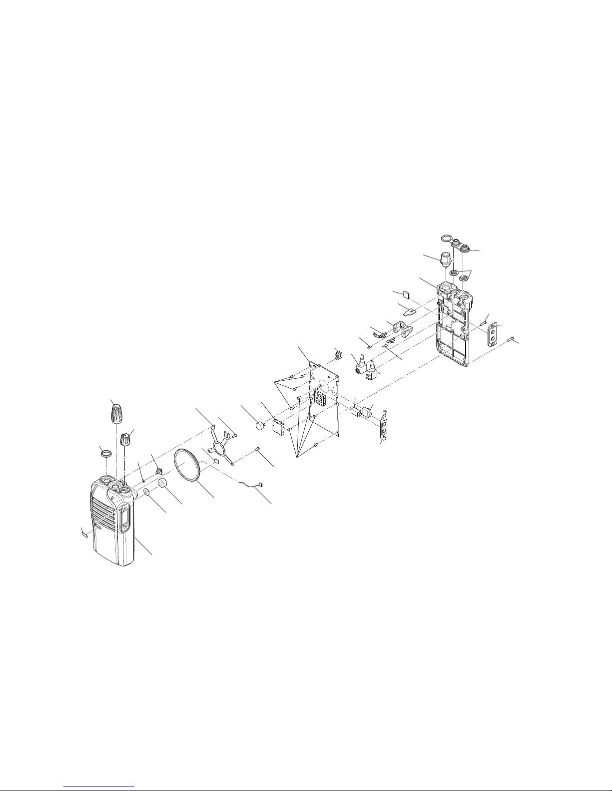
7 - 2
MP10(C)
MP18(C)
MP33(C)
S54(M)
MP16(C)
MP11(C)
MP12(C)
MP24(C)
MP27(C)
MP25(C)
SP1(C)
MP2(C)
MP1(C)
MP23(C)
MP22(C)
EP1(C)
J1(C)
MP13(C)
MC51(M)
MP2(M)
MP34(C)
MP34(C)
MP35(C)
MP32(C)
MP32(C)
J52(M)
J51(M)
MP21(C)
S51(M)
MP20(C)
MP31(C)
MP31(C)
MP19(C)
MP14(C)
MP17(C)
R421(M)
MP15(C)
W1(C)
ABBREVIATIONS:
(C): CHASSIS
(M): MAIN-A/MAIN-C UNIT
PCB
Page 31
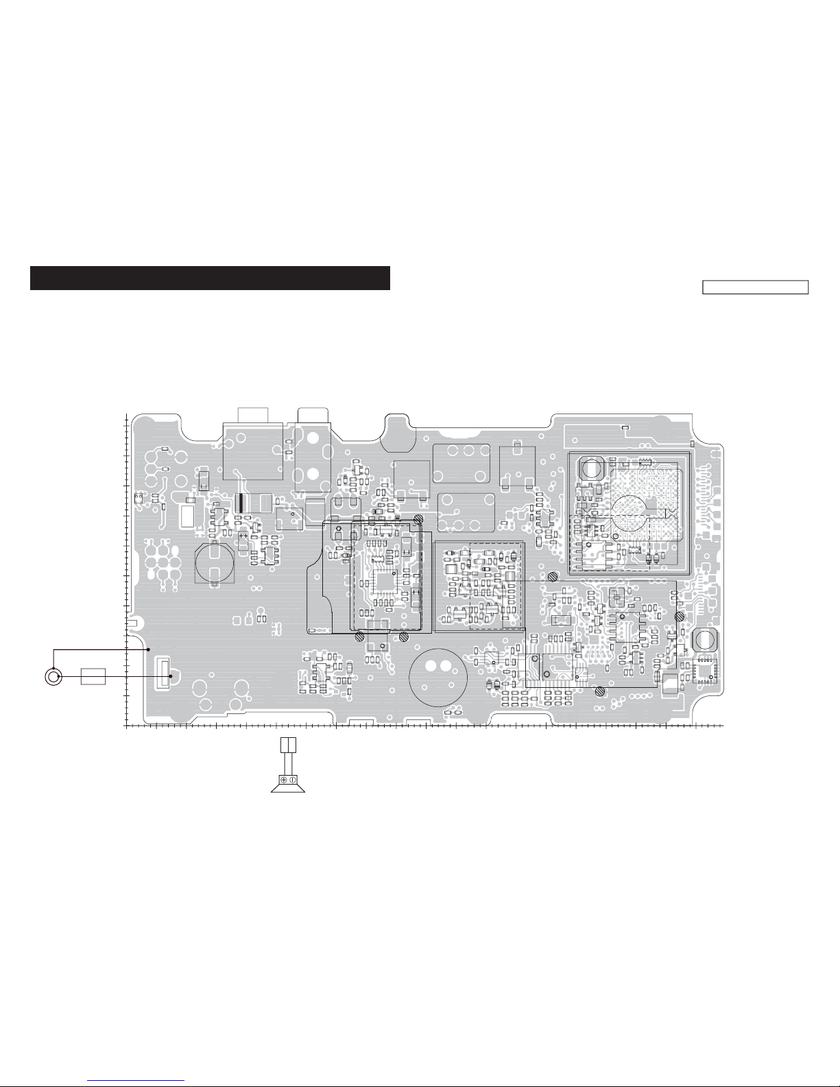
8 - 1
SECTION 8. BOARD LAYOUTS
• MAIN-A/MAIN-C UNIT
(TOP VIEW)
The combination of this page and next page shows
the top side and bottom side of actual P.C. board.
[MIC]
ANTENNA CONNECTOR
EP1 (CHASSIS)
J1 (CHASSIS)
[SP]
SP+ 1
SP− 2
SP1 (CHASSIS)
J53
MP10
MP13
MP14
MP7
MP3
MP6
MP8
MP12
C26
C27
C28
C30
C31
C32
C33
C34
C50
C66
C68
C71
C73
C74
C77
C78
38C18C
C84
C85
C86
C87
C88
C89
C90 C92
C101
C102
C103
C104
C105
C106
C107
C108
C110
C111
C127
C132
C134
C144
C145
C146
C147
C149
C150
C151
C152
C153
C154
C155
C156
C157
C158
C159
C160
C225
C232
C239
C246
C247
C248
C251
C252
C253
C254
C255
C256
C257
C286
C287
C288
C290
C292
C293
C300
C311C312
C313
C325
C376
C377
C378
C380
C381C382C383
C384
C385
C386
C395
C396
C397
C400
C406
C408
C412
C427
C428
C430
C431
C432
C433
C434
C435
C437
C447
C453
C454
C456
C457
C458
C463
C464
C465
C466
C467
C482
C483
C484
C486
C487
C488
C490
C491
C507
C508
C509
C510
C511
C513
C514
C900
C901
C907
C908
C909
C912
C913
C919
C920 C941
C958
D11
D12
D14
D15
D16
D32
D34
D53
D54
D901
D904
DS51
EP3
EP4
EP5
EP11
EP14
EP903
EP904
F51
FI2
FI3
FI4
FI5
IC1
IC4
IC21
IC52
IC53
IC54
IC58
IC62
IC63IC64
IC65
IC66
IC900
IC901
IC903
IC904
J51
J53
L23
L24
L31
L33
L36
L37
L40
L41
L42
L51
L900
MC51
MP3
MP9
Q8
Q10
Q13
Q14
Q26
Q29
Q67
Q82
Q83
Q85
Q90
Q91
R8
R9
R10R11
R12
R13
R14
R15
R16
R41 R42
R45
R46
R53
R54
R55
R56
R57
R64
R76
R77
R78
R79
R80
R81
R82
R83
R84
R87
R88
R123
R134
R135
R136
R148
R149
R171
R176
R177
R178
R181
R182
R183
R184
R185
R186
R187R188
R189
R364R367
R368
R369
R370
R373
R388
R389
R390
R405
R413
R422
R423
R424
R426
R427
R428 R429
R430
R437
R439
R441
R444
R451
R452
R453
R454
R455
R468
R469
R492
R493
R494 R496
R498
R610
R611R612
R620
R621
R622
R623
R624
R627
R628
R634
R635
R636
R637
R638
R639
R641
R651
R657
R688
R691
R692
R905
R906
R908
R910
R921
R930
R931 R932
R945
R951
R952
R953
R962
R968
R969
X1
X2
X51
B7413C
FUSE
J51
J52
IC2
X1
9
2
3
1
X51
-T1
-R5V
T2-
T5V
AFVO
PWON-
-VCC
-CL
-ADS
+3.3V
BAL-
REF
-MCG1
ATX
TMUT-
MCG0
TEMP
SIDE2
SIDE1
IPTT
DMO-
+5V
VCON
APCV
-TMUT
XPTT
IPTT
-T2
T5V-
-PAV
UHF
LVA
H0
H5H10H15H20
H25H30
H35H40H45H50H55H60H65H70H75
H80
H85H90H95
V0 V5 V10 V15 V20 V25 V30 V35 V40 V45 V50
Page 32

8 - 2
The combination of this page and next page shows
the top side and bottom side of actual P.C. board.
• MAIN-A/MAIN-C UNIT
(BOTTOM VIEW)
J51
J52
[VOL]
[PTT][Upper][Lower]
[ROTARY SELECTOR]
C1
C2
C3
C4
C5
C6
C7
C8
C9
C10
C11
C12
C13
C14
C15
C18
C19
C35
C36
C37
C38
C39
C45
C47
C48 C49
C51
C52
C53
C54
C55
C57
C59
C60
C61 C62
C63
C64
C65
C67
C72
C75
C76
C79
C80
C82
C91
C93
C94
C95
C96
C109
C112
C116 C117
C118
C119
C120
C121
C122
C123
C124
C141
C148
C167
C168
C171
C172
C173C175
C176
C177
C178
C179
C180
C181
C182
C183
C184
C186
C188
C189
C192 C194
C195
C196
C197
C198
C199
C200
C201
C203
C206
C208
C209C210
C211
C213
C214
C215
C216
C217
C218
C221
C223
C224
C226
C227
C231
C233
C235
C236
C238
C240
C241
C242
C243
C244
C261
C262
C263
C264
C265
C266
C267
C271
C272
C273
C274
C275
C276
C277
C282
C283
C284
C291
C318
C319
C322
C323 C324
C327
C328
C334
C335
C336
C337
C338
C339
C340
C341
C342
C343
C344
C361
C364
C388
C389
C390
C391
C392
C393
C394
C398
C399
C401
C403
C404
C405
C413
C418
C420
C423
C426
C429
C448
C451
C452
C455
C459
C461
C462
C468
C475
C485
C489
C492
C493
C494
C501
C502
C503
C504
C505
C506
C512
C515
C902
C903
C904
C905
C910
C911
C915
C916
C917
C918
C921
C922
C923
C924
C925
C926
C927
C928
C930
C931
C932
C933
C934
C935
C936
C937
C938
C939
C940
C942
C943
C944
C945
C946
C947
C948
C949
C950
C951
C952
C953
C954
C955
C956
C957
C959
D1
D2
D3
D5
D6
D10
D21
D22
D24
D26
D28
D31
D33
D36
D37
D38
D39
D51
D52
D55
D59
D60
D902
D903
D905
EP6
EP7
EP8
EP51
EP52
EP53
EP900
EP902
EP905
EP906
FI1
IC3
IC5
IC6
IC51
IC55
IC57
IC60
IC902
IC905
L1
L2
L3
L4 L5
L6
L7
L8L9
L11
L13
L14
L15
L16
L18
L19
L20
L32
L35
L46
L48
L901
MP4
MP5
MP11
Q1
Q2
Q3
Q4
Q9
Q11
Q12
Q15
Q16
Q17
Q21
Q22
Q23
Q24
Q27
Q28
Q51
Q52
Q58
Q59
Q63
Q64
Q66
Q71
Q72
Q73
Q81
Q84
Q86
Q87
Q88
Q92
Q93
Q95
Q900
Q901
R1
R2
R3R4
R5
R6
R21
R22
R23
R24 R27
R28
R29
R30
R31
R32
R33
R34
R35
R43
R44
R51
R52
R58 R59
R62
R65
R66
R67
R68
R69
R70
R71
R72
R73 R74
R89
R101
R102
R103
R104
R105
R106
R107
R108
R109
R110R112
R113
R114
R115
R116
R117
R118
R119
R120
R121
R122
R126 R127
R128
R132
R138R139
R140
R141
R142
R146
R147
R151
R152
R153
R154
R155
R156
R157
R158
R159
R161R162
R163
R164
R165
R166
R167
R169
R172
R173
R174 R175
R190
R243
R244
R357
R358
R359
R360
R361
R362
R363
R365
R366
R371
R372
R393
R394
R395 R396
R397
R398
R406
R408
R412
R414
R416
R417
R418
R420
R421
R431R432
R433
R434
R435
R436
R440
R442
R491
R495
R497
R499
R500
R502
R503
R504
R517
R518
R527
R614
R615
R616
R618
R619
R625 R626
R630
R631
R632
R633
R640
R646
R647
R652
R653
R661R662
566R466R366R
R666
R667R668R669
R683
R693
R694
R904
R907
R909
R911
R912
R913
R914
R915
R916
R917
R918
R919
R920
R922
R923
R925
R933
R934
R935
R936
R937
R938
R939
R940
R941
R946
R947
R948
R949
R950
R956
R957
R958
R961
R963
R964
R965
R966
R970
R971
R972
R973
R974
S52S53
X900
IC60
IC3
S52S53
S51
S54
R5V
+3.3V
T1-
VCC
-APCV
PDET-
TMUT
VCON
XPTT
-TMUT
MCG0
ATX
TXDO
RXDO
RXC
+3.3V
-NWC
OSS
SE
R SCK
T1-
+5V
CVDD 1.6V
DVDD 3.3V
AFVO
RSSI
S5C
PAV
T2
S5V
TEMP
-DET
+5V
BAL
TXC
T5V
H0 H5
H10
H15 H20
H25
H30 H35 H40 H45 H50 H55
H60
H65
H70 H75
H80
H85
H90
H95
V0V5V10V15V20V25V30V35V40V45V50
Page 33

9 - 1
SECTION 9. BLOCK DIAGRAM
LPF
LPF
SHIFT
SW
D60
1SS390
ANT
SW
D22:HVD142A
D3:HVD142A
PWR
AMP
Q1
RD07MUS2B
TX/RX
SW
D6:HVD142A
D5:HVD142A
Q13 2SC4226
D12 HVD350B
Q14 2SC4226
D16 HVD350B
FIL
RIPPLE
Q15
2SC4116
FIL
LOOP
PLL
IC
IC4
AK1541
X3
Q26
2SC4116
X1
JTBM450CX
X51
CR-912
FM
MOD
D15
1SV309
Q23
3SK293
BPF
D28
HVB350BYPTL
BPF
D28
HVB350BYPTL
BPF
D26
HVB350BYPTL
BPF
D24
HVB350BYPTL
BPF
RF
AMP
Q22
3SK293
APC
AMP
IC1
TA75S01F
BPF
XTAL
FI1
FL-442
IF
AMP
Q24
2SC5107
BUFF
Q8
2SC5107
BUFF
Q10
2SC5107
BUFF
Q9
2SC5107
BUFF
Q17
2SK880
DRIVE
AMP
Q2
RD01MUS1
GATE
CTRL
Q21
2SK1829
S51
X2
CR-892
TCXO
LV
ADJ
D11
HVD350B
LED
CTRL
Q82:Q83
LDTA144EE
R
G
DS51
LNJ115W8PRA
SELECT
S54
TP70TF5169
CH
W/N_D
SW
D38,D39:1SS390
Q27:LDTC114YE
BPF
CERAMIC
FI3
LTM450FW
BPF
CERAMIC
LTM450HW
FI4
W/N_D
SW
D36:D37
1SS390
BUFF
Q28
2SC4116
AMP
IC5
NJM2711F
BPF
CERAMIC
FI5
LTUCG450G
EEPROM
IC52
R1EX24512ASAS0A
RESET
IC53
NJU7704F3
BPF
XTAL
FI2
FL-448
A/D
SW
D33,D34:HVD144A
Q29:LDTC114YE
PRE
AMP
Q4
2SC5107
DRIVE
PRE
Q3
2SC3356
LPF
LV
ADJ
D14
HVD396C
VCO
SW
Q12:LDTC144EE
Q95:LDTC114EE
PWR
DET
D1:LRB751S
D2:LRB751S
A/D
SW
D31:D32
HVD144A
AMP
IC21
TA75S01F
Q901
LDTC114YE
LPF
IC60
NJM13403V
LPF
IC60
NJM13403V
BUFF
IC60
NJM13403V
J52
AF
AMP
IC55
TPA0211
D51:LRB706F
Q81:LDTC144TE
CLONE
BUFF
PWR
CTRL
Q63:2SB1132
Q64:DMC506010R
AMP
IC58
TA75S01F
J53
1
2
AF
AMP
IC12
TA7368F
SP1
LIMIT
AMP
IC60
NJM13403V
MOD
LINE
IC66
CTRL
TC7W53FK
J51
AUTO_TX
CTRL
Q59
LDTC114YE
DET
D53
L1SS400
AMP
IC64
NJM12904V
ALC
AMP
IC63
NJM2783V
MC51
PTT
DET
Q58
DRA9123Y
A/D
SW
LDTC114YE
Q67
AMP
IC64
NJM12904V
MIC
GAIN
IC62
CTRL
TC7W66FK
HPF
IC63
NJM2783V
AMP
IC905
NJM2711F
TCXO
12.288MHz
X900
CR-914
SHIFT
SW
Q900
LDTA144EE
FLASH
EN25Q40
IC904
A/D
IC901
ADS7886
R88
AF VOL
R1
LINE
FILTER
DC-DC
1.6V
IC900:TPS62204
S5
REG
Q71:KTA2015
Q86:LDTC114YE
DC-DC
3.3V
IC65
BD9141MUV
BATTERY_1
BT1
LINE
FILTER
REG
R5
Q72:2SA1586
Q87:LDTC114YE
REG
+3.3V
Q90:2SA1577
Q91:LDTC114YE
REG
+5V
IC54
NJM2871BF05
LINE
FILTER
REG
T5
Q73:KTA2015
Q88:LDTC114YE
LINE
FILTER
SW12
S5
Q92:TPC6103F
Q93:LDTC114YEPOWER
SW D59:LDAN222
F51
12
VCO
SW
Q11
LDTC114EE
A/D
SW
Q66
2SK3019
RES
IF IC
LVIN
S5V R5V
RX VCO
TX VCO
RSSI
T2
T1
T1
NOIS
IC3:NJM2591V
450-520MHz
15.3MHz
45.9MHz
DISC
SQIN
46.35MHz
19.6608MHz
CSFT
MIXER
RSSI
CPUV
LV
LVA
S52
S53
450kHz
450kHz
NWC
IPTT
MOD
DIF
ADS
RXC
LVA
SSO
SCK
PLST
LINEAR
DMO
RLED
TLED
CBI0 CBI1
CBI2 CBI3
SIDE1
SIDE2
CLO
UNLK
SCK
PLST
UNLK
SSO
ESCL
ESDA
CODEC
IC902
PCM3008
BCLKX1 BFSX1
BDX1 BDR1 PWADN
IC51
HD64F2506RBR26DV
CPU
SSO
SCK
DAST
VCON
CLI
CLI
CLO
DAST
PLSW
NWC
ADS
TMUT
LVIN
RSSI
NOIS
S5C
VOXV
MDET
BEEP
ATX
MCG0PWON
TXC
MCG1AFON
RXC
400-470MHz
403.65MHz-473.65MHz
353.65MHz-423.65MHz
350-400MHz
303.65MHz-353.65MHz
DET
DISC W/N SW
AFVO
MOD
VREF
BAL
VCON
REF+5V
SSO
SCK
DAST
D/A
AK2330
IC57
DET SQIN
T1 T2 LVA
AFON
CL
AFON
MDET
AFOAFVO
VCC
MCG0
DMI
ADS
VOXVATX
XPTT
MCG1
DIF
VREF
TM320VC5509AZHH
IC903
BDR0
BCLKR0
BFSR0
BDR0 BDX0
FCS BCLKX0
TEMP
POSWH
AFVI
DPDN
DRES
DSIRQ
DSS
DSCK
DMOSI
DMISO
CPUV
+3.3V
RXC
PWON
T5V
CVDD_1.6V
VCC
R5V
+3.3V_A
3.3V_VDD
DVDD_3.3V
VCC
TXC
+3.3V
CPUV
POSWH
+5V
S5C
DAFO
BEEP
DMO
DAFO
DSP
DCSFT
CLKIN
BATV
XPTT
PWON
PWON
S5C
S5V
ADS
Page 34

10 - 1
SECTION 10. VOLTAGE DIAGRAM
• MAIN-A/C UNIT (1/3)
TX 0.82V
RX 0V
TX 4W 2.26V
TX 1W 0.98V
RX 0V
TX 1.66V
RX 0V
TX 4.89V
RX 0V
TX 4W 3.50V
TX 1W 1.56V
RX 0V
TX 4W 1.76V
TX 1W 1.25V
RX 0V
TX 0.70V
RX 0V
TX 1.34V
RX 1.34V
TX 1.99V
RX 0V
TX 0V
RX 1.99V
7.50V
0.78V
0.76V
4.51V
4.98V
4.24V
0.77V
TX 1.72V
RX 0V
TX 0V
RX 1.73V
TX 1.75V
RX 2.43V
LOCK 3.23V
UNLOCK 0V
15.3MHz
1.06Vp-p
W 2.74V
N 0V
TX 0V
RX 0.59V
TX 0V
RX 4.69V
TX 0V
RX 3.27V
A 2.69V
D 0V
TX 0V
RX 0.55V
TX 0V
RX 0.65V
TX 0V
RX 1.77V
R138
470
R147
1.5K
R132
10K
R146
47
IC1
TA75S01F
1
2
3
4
5
R82
10K
R13
10
Q26
2SC4116
R151
27K
R152
8.2K
R155
27K
IC3
NJM2591V
1
OSCIN
2
OSCOUT
3
MIXOUT
4
V+
5
IFIN
6
DEC
7
FILOUT
8
FILIN9AFOUT
10
QUAD
11
IFOUT
12
RSSI
13
NOISEDET
14
NOISEREC
15
GND
16
MIXIN
EP5
MMZ1005Y102CT
R80
EXB28V102J
EP4
MMZ1005Y102CT
NOIS
SQIN
TMUT
S5V
NWC
MOD
HV
R5V
+5V
SCK
DISC
T5V
UNLK
LVIN
PLST
VCON
SSO
RSSI
D36
1SS390
D37
1SS390
D38
1SS390
D39
1SS390
FI1
FL-442
1
IN
2
OUT3GND
4
GND
56
MP3
2775
123
4
R153
3.3K
R154
8.2K
C235
10
R148
1K
C231
100P
C251
3P
C252
56P
C254
56P
C256
10P
C158
10P
C155
47P
C154
47P
C153
47P
ANT_BOARD
FI4
LTM450HW
IO
X1
JTBM450CX70
C33
0.001
C32
0.001
C28
0.001
C26
0.001
C27
0.001
C224
0.001
C236
0.001
C238
0.001
C240
0.001
C160
0.001
C152
0.001
C264
0.01
C265
0.01
C263
0.01
R149
680K
C91
1
C31
0.1
C227
0.01
C226
0.01
C255
0.01
C257
0.01
C159
0.1
C156
0.1
C244
0.1
C239
330P
C253
6P
MP4
OG-503040
R140
3.9K
R175
560
C218
0.01
R9
10K
R8
22K
C30
0.22
C267
0.1
R172
10
FI3
LTM450FW
IO
Q28
2SC4116
IC4
AK1541
1
CPVDD
2
TEST4
3
TEST1
4
LE
5
DATA
6
CLK
7LD8
PDN29PDN110REFIN11TEST212TEST3
13
VREF1
14
DVSS
15
VREF2
16
RFINN
17
RFINP
18
PVDD
19
BIAS20PVSS
21CP22
CPZ
23
SWIN
24
CPVSS
25
C271
0.1
C272
0.1
C273
0.1
R162
100
R161
180K
R190
1K
IC5
NJM2711F
1
2
3
4
5
R165
1.5K
R167
6.8K
R166
5.6K
R163
100
C275
0.033
C276
27P
R164
4.7K
C274
0.1
C277
0.1
C284
0.01
C290
0.01
C282
0.01
C286
0.01
R173
3.3K
R174
3.3K
R177
1K
C291
0.1
C292
0.1
C293
0.001
C146
0.22
C145
0.22
C144
100P
R81
27K
C151
100P
C150
0.01
C148
10
R84
100K
X2
CR-892(15.3MHZ)
1
VCON2GND
3
OUT4VCC
ADS
T1
T2
LVA
DIF
S5C
PLSW
+3.3V
R134
100K
C147
0.001
R16
10K
C266
0.1
C261
0.01
C262
0.01
L23
MLG1608S
L24
MLG1608S
R158
4.7K
Q29
LDTC114YE
Q27
LDTC114YE
IC6
TC7W66FK
1
2
3
4
5
6
7
8
R169
1.5K
R58
100K
RXC
Q16
LDTC114YE
D31
HVD144A
D32
HVD144A
D33
HVD144A
D34
HVD144A
C8
2.5P
C4
1.5P
R2
2.7K
R5
2.7K
L3
0.30-0.9-5TL
L1
0.30-0.9-6TR
R4
1K
R1
68K
C1
1.5P
C10
0.001
R3
1K
L2
0.30-0.9-6TR
C2
8P
C7
0.001
C171
4P
L11
LQW18AN22NG00
C172
2P
D22
HVD142A
C173
0.001
C175
47P
R105
10K
C181
7P
R156
1K
R104
10K
R106
47K
D26
HVB350BYPTL-E
1
2
3
4
C183
0.001
C179
6P
C184
0.1
D24
HVB350BYPTL-E
1
2
3
4
C177
8P
C182
0.001
L15
LQN21A
D21
L1SS400
R102
470K
C192
0.001
R112
47
R109
10
R108
82K
C188
0.001
Q22
3SK293
C189
0.001
R103
1.8K
Q21
2SK1829
*R113
R110
100
C194
0.001
L16
LQN21A
R115
100K
R114
100K
R116
120K
C198
12P
R157
1K
C203
0.1
*C200
R159
12K
C197
0.5P
D28
HVB350BYPTL-E
1
2
3
4
C196
12P
C201
0.001
C221
47P
R118
120K
C211
0.001
R119
150K
R122
47
C217
0.01
C216
0.001
R121
3.3K
R117
100K
C215
18P
L20
ELJNC
L19
MLK1005S
C223
0.001
R120
120
Q23
3SK293
C213
47P
C214
0.001
R139
100K
C233
47P
C225
0.01
C19
0.001
Q1
RD07MUS2B-T112
C45
47P
L6
0.40-0.9-2TL
L7
0.40-1.4-5TR
C18
0.001
L4
NLV25T
R21
10
C49
0.001
C38
0.001
C36
47P
L5
0.40-0.9-2TL
C37
330P
R6
220
C11
0.001
C39
47P
D3
HVD142A
Q2
RD01MUS1-T113
EP6
MPZ2012S331A
L48
MLK1005S
R23
33K
R22
4.7K
C52
0.001
R29
47
C54
0.001
R30
22K
L8
MLK1005S
C55
10P
C57
330P
C51
4P
*R28
R24
47
R27
4.7K
*C34
C35
0.001
C65
0.001
R35
4.7K
R31
100
D5
HVD142A
C59
5P
R33
10K
C61
0.001
C67
2P
L9
MLK1005S
C60
47P
R34
100
C64
0.001
C71
10P
D6
HVD142A
*C206
C208
2P
L18
MLK1005S
C209
2P
C210
5P
C168
7P
C167
7P
L46
MLK1005S
R83
56
C149
100P
L31
MLK1005S
R41
10
R42
68K
C72
0.001
C74
5P
C73
0.001
R43
100
C81
3P
R44
100K
C76
0.001
C82
47P
L32
MLK1005S
C141
6P
L33
MLK1005S
C66
2P
R45
100
C78
0.001
R46
100K
C79
0.1
C77
0.001
Q11
LDTC144EE
EP11
MMZ1005A152ET
C83
0.75P
C101
0.5P
EP14
MMZ1005A152ET
Q12
LDTC144EE
C80
330P
C122
0.01
Q15
2SC4116
C121
10
R67
2.2K
C85
0.001
C87
18P
EP3
MMZ1005Y102CT
C84
330P
MP5
OG-503040
C109
0.001
D12
HVD350B
C93
330P
D15
1SV309
C94
47P
D16
HVD350B
L41
LQW18ANR47G00
R64
10
R87
100K
C110
0.5P
C120
0.001
C124
0.001
R68
470K
R66
150K
R65
27K
C118
47P
R72
100
C123
0.001
R71
10K
Q17
2SK880
C116
1
C186
0.1
C47
330P
FI2
FL-448
1
IN
2
OUT3GND
4
GND
56
C288
9P
R74
6.8K
R73
10K
C157
0.001
IC21
TA75S01F
1
2
3
4
5
R188
100K
C248
0.1
R189
100
R187
100K
R181
150
R182
2.2K
R183
2.2K
R127
120K
R126
100
FI5
LTUCG450G
DET
Q95
LDTA144EE
Q3
2SC3356
C112
0.001
R52
470
R185
100K
R186
270K
C247
39P
R178
5.6K
R176
22K
R171
22K
C117
0.0015
R135
1.5K
R136
1.5K
C232
33P
CP1
C246
10
R78
0
R79
1.2K
R77
2.2K
C134
0.47
R76
120
C132
0.33
R59
270K
R62
120K
R142
120K
R141
68K
R123
0
C287
4P
R184
10
L37
LQW18ANR47G00
L42
LQW18ANR47G00
EP7
MMZ1005A152ET
EP8
MMZ1005A152ET
C195
2P
C199
2P
C12
9P
R14
270
R15
1K
R12
470K
R10
100K
C89
12P
D11
HVD350B
L36
0.30-0.9-4TR
C86
5P
C107
12P
C106
12P
R57
0
C105
10P
L35
MLG1608S
C241
33P
Q13
2SC4226
Q14
2SC4226
C119
1
R107
27K
Q4
2SC5107
Q8
2SC5107
Q9
2SC5107
Q10
2SC5107
Q24
2SC5107
C48
47P
C50
47P
C68
0.001
C75
47P
C95
47P
D10
MA2S7280G
L40
0.30-0.9-3TR
C176
27P
C180
33P
C178
2P
C63
5P
R32
22K
C62
8P
C13
15P
C9
3P
C5
7P
D2
LRB751S-40T1G
D1
LRB751S-40T1G
C3
1P
C6
1P
R11
82K
C242
150P
C243
150P
C283
6P
R128
680
C104
5P
C108
3P
C111
8P
C92
15P
C88
10P
C90
0.5P
R51
470
R70
220K
R69
150K
C127
0.001
C103
47P
C102
0.001
C14
27P
D14
HVD396C
R53
6.8K
R54
6.8K
R55
6.8K
R56
6.8K
C53
330P
*C300
L13
LQN21A
L14
LQN21A
*C15
*C96
R101
220K
PLST
SSO
SCK
R5V
S5V
+5V
HV
UNLK
NOIS
DISC
LVIN
SQIN
VCON
MOD
TMUT
NWC
RSSI
PLST
SCK
SSO
T5V
T2
+5V
VCON
DET
S5C
+5V
UNLK
R5V
DIF
ADS
LVA
T1
T2
R5V
ADS
TMUT
DIF
R5V
S5C
PLSW
RSSI
+3.3V
+3.3V
+3.3V
T5V
S5V
PLSW
RXC
NWC
T1
RSSI
R5V
R5V
S5V
VCOV
MOD
T5V
LVIN
R5V
DET
RXC
+3.3V
LVA
NOIS
SQIN
DISC
APCV
T1
+5V
+5V
HV
PAV
LPF
APC
AGC
RF AMP
MIX
IF AMP
IF IC
REF
T5V
R5V
HV
T5V
*3 MULTI
PLL
S5V
HV
T5V
L:NARROW H:WIDE
TX VCO
RX VCO
*: Refer to the PARTS LIST for the value and name of component.
Page 35

10 - 2
• MAIN-A/C UNIT (2/3)
*: Refer to the PARTS LIST for the value and name of component.
TX 0V
RX 4.82V
TX 4.89V
RX 0V
TX 0V
RX 3.32V
TX 3.32V
RX 0V
AFON 5.27V
OFF 0V
19.66MHz
1.73Vp-p
2.23V
1.43V
3.28V
3.32V
5.00V
C453
15P
IC66
TC7W53FK
1
COM
2
INH
3
VEE
4
GND5A
6
CH1
7
CH0
8
VCC
R468
680
Q90
2SA1577
IC60
9
10
8
R668
EXB28V102J
R243
10
CP6
Q52
LDTC114YE
R373
100K
C323
0.1
R625
270K
CP8
C389
0.001
R639
100K
IC54
NJM2871BF05
1
CTRL
2
GND
3NB4
VOUT
5
VIN
C338
0.001
R969
1M
C311
1
J53
1
2
34
R414
330K
Q88
LDTC114YE
R244
1M
C435
22
IC60
V+
4
GND
11
C398
0.001
ADS
R692
1K
R634
10K
R439
150K
IC55
TPA0211DGN
1
IN
2
SHUTDOWN
3
VDD
4
BYPASS
5
VO+
6
SE/BTL
7
GND
8
VO-
9
C344
0.1
C461
0.1
R640
100K
C491
0.01
DIF
C457
0.027
IC65
BD9141MUV
1
SW
2
SW
3
SW
4
SW
5
SW
6
PVcc7PVcc8PVcc
9NC10
Vcc
11
GND
12
ADJ
13
ITH
14
VREG
15
NC
16NC17EN18
PGND19PGND20PGND
21
R517
1.8K
R413
100K
CP15
T2
R527
100K
C514
1
R452
47K
R641
100K
R432
4.7K
R657
1K
Q73
KTA2015
CP16
CP132
C388
0.001
NOIS
C405
1
SQIN
DSCK
R436
4.7K
R365
4.7K
UNLK
D59
LDAN222
C448
10
R632
10K
R646
100K
C512
1
R651
1K
DPDN
Q86
LDTC114YE
C463
0.1
Q59
LDTC114YE
R371
100K
C400
10
R683
1K
C431
100
R422
100K
D51
LRB706F
R423
33.0K
R405
1.8
DMOSI
R638
100K
C433
0.001
C452
0.1
CP17
R361
5.6K
CP10
C361
0.1
J51
R408
100
C503
0.1
DRES
CP5
EP53
MMZ1005A152ET
RSSI
C482
0.068
R669
EXB28V102J
VREF
C376
0.001
S5V
C319
0.1
DET
R492
5.6K
R624
10K
C339
0.001
C484
1
R627
100K
C502
0.1
DMISO
R623
5.6K
CP20
C335
0.001
PLSW
R630
0
D54
L1SS400
C456
0.1
CP13
C429
0.01
Q85
LDTC114YE
R612
100K
D52
MA2S7280G
Q72
2SA1586
+5V
C318
0.01
R494
47K
R498
18K
R366
150K
R652
1K
C391
47P
R618
10K
R637
10K
C406
0.001
R433
10K
R653
1K
C511
1
R434
10K
SCK
C426
0.01
L51
VLCF4028T-4R7N1R5-2
R389
3.90K
CP7
DSIRQ
Q83
LDTA144EE
R370
470K
R424
15.0K
R635
10K
D53
L1SS400
C384
1
MOD
PLST
R
YG
DS51
LNJ115W8PRA
C394
0.001
TMUT
Q93
LDTC114YE
CP11
R440
390
CP12
C437
0.001
C515
0.001
R89
100K
C336
1
C404
0.1
C397
0.001
C423
0.01
R435
10K
R420
100K
R693
15K
R362
33K
C504
0.1
C378
0.001
R360
2.2K
R417
1.2K
C490
0.068
IC57
AK2330
1
VIN7
2
VIN0
3
VOUT0
4
VOUT1
5
VIN1
6
RSTN
7
CSN
8
SCLK
9
SDATA
10
DVDD
11
VSS
12
AVDD
13
VREF
14
VIN2
15
VOUT2
16
VOUT3
17
VIN3
18
VIN4
19
VOUT420VOUT521VIN522VIN623VOUT624VOUT7
25
MP11
OG-503040
C505
0.1
C507
1
SSO
R364
47K
R496
82K
R647
1K
IC53
NJU7704F3-28A
1
CD
2
VSS
3
MR4VOUT
5
VDD
C401
0.1
D55
L1SS400
R611
0
C451
0.1
C413
0.001
DISC
R614
120K
R416
1K
R372
100K
C465
NFM18PC104R1C3
C342
0.001
C390
0.001
C427
0.1
R622
18K
C343
10
C408
0.1
IC62
TC7W66FK
1
2
3
4
5
6
7
8
LVA
Q71
KTA2015
IC63
NJM2783V
1
GAIN1
2
GAIN2
3
DET
4
OUT
5
BUFFIN
6
BUFFGAIN
7
BUFFOUT8GND
9
V+
10
VREF
11
SENSE
12
INT
13
GAINSW
14
IN
C430
0.1
R503
100
R5V
C327
0.012
R369
150K
T5V
S51
SW-149
C510
0.001
J52
Q91
LDTC114YE
R406
100K
C488
1
C313
0.1
VCON
DMO
CP9
R694
15.0K
X51
CR-912
C340
0.1
R437
100K
+3.3V
CP18
R636
10K
Q92
TPC6103
1
2
3
4
5
6
D60
1SS390
R442
330
IC60
2
3
1
R431
10K
C455
15P
R444
1K
T1
R493
10K
R453
47K
Q67
LDTC114YE
C380
68P
R367
27K
C337
0.001
Q63
2SB1132
HV
C454
6P
R441
10K
R620
47K
IC60
13
12
14
R518
100K
DAFO
C393
220
C322
1
IC64
V+
8
GND
4
IC58
TA75S01F
1
2
3
4
5
R628
100K
Q87
LDTC114YE
CPUV
C506
0.1
C509
1
NWC
R430
1M
R968
100K
R88
ERTJ0EP473J
LVIN
IC64
6
5
7
C513
0.1
C458
0.47
CP19
C392
47P
Q84
LDTC144EE
C334
0.001
R428
1K
R662
EXB28V102J
C412
0.001
C399
0.1
C489
1
C432
0.001
DIF
R368
270K
DMI
EP51
MMZ1005Y102CT
C377
22
C501
0.1
R661
EXB28V102J
C328
270P
R663
EXB28V102J
C508
0.001
C385
0.1
Q51
KTA2015
C395
220
R633
4.7K
S5C
+3.3V
IC60
NJM13403V
6
5
7
C428
0.001
Q82
LDTA144EE
C483
1
R666
EXB28V102J
IC64
NJM12904V
2
3
1
EP52
MMZ1005A152ET
R363
470
CP21
C466
1
DSS
RXC
IC51
HD64F2506RBR26DV(EMPTY)
A1
A2
A3
A4
A5
A6
A7
A8
A9
A10
A11
A12
A13
A14
A15
B1
B2
B3
B4
B5
B6
B7
B8
B9
B10
B11
B12
B13
B14
B15
C1
C2
C3
C5
C7
C8
C13
C14
C15
D2
D3
D4
D6
D7
D8
D9
D10
D13
D14
D15
E1
E2
E3
E4
E12
E13
E14
E15
F1
F2
F3
F4
F12
F13
F14
F15
G1
G2
G3
G4
G12
G13
G14
G15
H1
H2
H3
H4
H12
H13
H14
H15
J1
J2
J3
J4
J12
J13
J14
J15
K1
K2
K3
K4
K12
K13
K14
K15
L1
L2
L12
L14
L13
L15
M1
M2
M3
M4
M5
M6
M7
M8
M9
M10
M11
M12
M13
M14
M15
N1
N2
N3
N4
N5
N6
N7
N8
N9
N10
N11
N12
N13
N14
N15
P1
P2
P3
P4
P5
P6
P7
P8
P9
P10
P11
P12
P13
P14
P15
R3
R4
R7
IC52
R1EX24512ASAS0A
1
A0
2
A1
3
NC
4
VSS5SDA
6
SCL
7
WP
8
VCC
+5V
R631
10K
C487
1
CP14
R665
EXB28V102J
R691
100K
C467
1
R626
100K
R667
EXB28V102J
R621
15K
R455
0
R615
22K
R451
33K
R619
27K
C324
820P
R454
120K
C312
180P
R412
10K
C403
0.22
C485
1
R504
100K
R491
22K
R497
22K
C492
100P
Q81
LDTC144TE
C493
680P
R500
39K
R388
27K
R390
8.20K
C325
0.01
R688
2.2K
R664
EXB28V471J
R418
390
R616
150K
Q58
DRA9123Y0
R469
270
C381
0.1
C382
0.1
C383
1
R426
2.7K
R427
15K
R421
F081165S-5
R495
47K
R502
470K
R499
6.8K
C494
0.01
R610
82K
C386
0.1
C459
NFM18PC104R1C3
C462
47
C464
47
C468
47
S52
SW-167(SKQT)
S53
SW-167(SKQT)
R394
82K
R395
27K
C418
47P
C420
47P
C486
0.1
Q64
DMC506010R
1
2
3
4
5
6
Q66
2SK3019
MC51
EM9745P-33-G
R398
150K
C364
100P
R397
150K
R393
470K
R396
180K
F51
ERBSE3R00U
12
R357
22K
C341
1
R358
390
R359
8.2K
S54
FSR080453W-01+16C
1A12
C1
3
B1
4A25
C2
6
B2
7A38
C3
9
B3
C447
100P
C475
100P
C434
0.01
C396
100P
R429
560K
TXC
RES
A7
A15
B8
M15
MSEL
L1
BAL
+3.3V
RXC
PLST
D6
C13
RXD0
AFON
A7
S5C
B15
B12
TXD0
MOD
MCG0
P4
D7
TLED
DSCK
P4
C1
C7
L15
SIDE1
R4
D3
D7
L14
+3.3V
SIDE2
SCK
J2
MDET
PLSW
M1
D2
AFVI
DET
J1
DIF
M8
+3.3V
DET
H2
+3.3V
BEEP
TXD0
LVIN
SQIN
DISC
N14
ADS
DAFO
MOD
M1
UNLK
C2
MD2
RSSI
H1
DMO
L2
CPUV
N4
LVIN
AFVI
DMISO
DMI
AFON
RXC
SCK
CL
NMI
DIF
IPTT
+5V
DSIRQ
SCK0
J1
+5V
NOIS
S5C
ATX
M2
DMISO
B8
MDWN
ADS
MDET
LVA
T2
M2
M8
DMOSI
SIDE1
H2
SSO
VREF
D14
T1
J2
REF
VCON
DSCK
CLI
VOXV
H1
TXC
CLO
MD2
DMI
XPTT
T1
T2
DSS
+3.3V
DSIRQ
DMO
C2
8P
SIDE2
MCG0
AFON
LVIN
VREF
CL
N14
S5V
C8
ADS
CPUV
VOXV
PLSW
LVA
H12
P15
CBI2
S5V
+5V
R5V
M14
TLED
D13
CPUV
CBI2
IPTT
NWC
ESDA
POSWH
TEMP
VREF
M15
RLED
A15
CBI1
H12
+5V
AFVO
CBI3
+3.3V
AFVI
D8
T5V
RSSI
C14
A5
VREF
ATX
TMUT
TMUT
BATV
MD2
+5V
BATV
DAST
B12
+5V
DRES
CBI0
CLO
RES
C5
PWON
NWC
R3
CBI0
VCC
CLI
SSO
RLED
VOXV
REF
HV
+3.3V
MCG1
+5V
DAST
SSO
A5
C5
7P
CBI3
PWON
TLED
R5V
+5V
SCK
VCC
DPDN
N4
B15
RSSI
PLST
POSWH
XPTT
C15
SQIN
T5V
PWON
RXD0
UNLK
CBI1
VCON
CPUVCPUV
DAFO
ESCL
DMOSI
BATV
PWON
RXC
VREFVREF
TEMP
C15
DRES
RLED
D8
DSS
+3.3V
NOIS
D13
T5V
DPDN
T5V
+5V
TEMP
RES
S5C
+5V
M14
NMI
P15
AFVO
BEEP
RES
VCC
+5V
+5V
+5V
+5V
VCC
ADS
HV
VREF
DSIRQ
LIMITTER
PLSW
ESCL
AFON
TXD0
DAST
ESDA
PLST
Ana
AFVI
MCG0
PWON
DMOSI
BATV
TEMP
VOXV
TXC
DMISO
POSWH
RLED
CBI1
300Hz HPF
DSS
A
BTL AMP
DPDN
CBI0
DRES
NWC
B
NOIS
ADS
RMUT
DSCK
LVIN
RSSI
SIDE1
A
B
CBI3
RXD0
S5C
L:Dig/H:Ana
5V REG
VOX AMP
SSO
MIC AMP
MCG1
IPTT
D
3.3V DC-DC
C
XPTT
SCK
BEEP
RXC
6dB/oct
TMUT
TLED
Dig
SIDE2
CSFT
CBI2
ATX
UNLK
SCK0
ALC(Digital Only)
Page 36

10 - 3
• MAIN-A/C UNIT (3/3)
*: Refer to the PARTS LIST for the value and name of component.
12.288MHz
1.14Vp-p
1.43V
3.27V
1.58V
3.27V
R916
47K
C946
0.1
CP118
R958
100K
C926
0.001
R930
47K
C934
4.7
C920
0.01
C955
0.1
C918
0.01
C944
0.1
R972
0
C953
0.001
CP111
R909
100
C932
0.1
IC902
PCM3008T
1
VCOM
2
VINR
3
VINL
4
GND
5
VCC
6
DEM0
7
DEM1
8
DOUT9DIN
10
LRCK
11
SYSCK
12
BCK
13
PDAD
14
PDDA
15
VOUTL
16
VOUTR
C952
22P
D904
MA2S7280G
R914
0
C950
10P
R941
47K
R947
EXB28V104J
R910
47K
+3.3V
R918
47K
C921
4.7
DAFO
C940
4.7
C937
0.01
C903
NFM18PC104R1C3
C907
0.001
IC903
TMS320VC5509AZHH
H11
M7
K7
K6
P6
M6
N5
P4
N4
P3
N3
K9
M8
P7
P5
K1
H3
G3
F10
E12
D14
D13
D12
E11
C14
B14
C13
G5
G2
G4
H1
H4
H5
J1
J3
J4
K2
M1
K3
M2
F5
B5
A6
B2
B7
B8
G1
J10
J11
J5
M11
M4
N7
N8
K8
P9
M9
P10
M10
P11
N11
L10
P12
N12
M14
L12
D4
A4
A8
D9
E3
E6
F13
H10
H2
J2
K10
M12
N13
N6
P13
P14
P8
E7
K11
K12
A5
B6
F3
E1
E2
B3
A3
C4
G14
G13
G10
F14
F12
E10
C12
15P
A13
A14
B13
H12
A12
B12
D7
D8
A7
E9
C8
4P
E8
A9
A10
C9
5P
A11
B10
H14
H13
J13
K14
K13
B4
J14
J12
G11
G12
A2
B1
B11
B9
E13
E4
E5
F11
F4
K4
K5
M13
M3
M5
N1
N10
N14
N2
N9
P1
P2
F1
F2
E14
R963
100K
R905
22
D901
MA2S7280G
R933
47
C917
0.1
C904
NFM18PC104R1C3
C912
4.7
R921
0
C916
10
DMOSI
C941
0.1
L901
ELJFC
IC901
ADS7886SDCKR
1
VDD
2
GND
3
VIN4SCLK
5
SDO
6
CS
R906
8.2K
DRES
R923
1K
C956
5P
EP900
MMZ1005S601CT
R932
47K
C913
0.1
R957
100K
R945
EXB28V104J
L900
VLCF4028T-100M1R0-2
C936
1
EP905
MMZ1005S601CT
CP112
C922
4.7
C909
0.1
R931
47K
C923
0.01
C958
0.1
C938
47P
CPUV
C925
47P
C933
0.1
D905
MA2S7280G
DMO
R915
100K
R934
47K
R912
100
R952
100K
C928
1
VREF
R962
100K
DSCK
C908
4.7
C905
NFM18PC104R1C3
DPDN
R949
EXB28V104J
EP904
MMZ1005S601CT
CP114
R966
100K
C910
0.1
R936
47K
R919
47K
R961
100K
DMI
IC905
NJM2711F
1
2
3
4
5
EP903
MMZ1005S601CT
C949
47P
DISC
R948
EXB28V104J
C945
0.1
R951
EXB28V104J
C931
1
EP902
MMZ1005S601CT
CP117
R935
47
R953
100K
R907
8.2K
R946
EXB28V104J
C939
47P
C901
4.7
CP128
R922
100
C900
0.1
R937
47K
CP113
CP900
R939
2.2K
C911
10
R917
100K
R913
100
D902
MA2S7280G
DMISO
C957
0.1
C959
10P
R970
0
C942
0.1
C947
0.1
+5V
R956
0
IC900
TPS62204DBVR
1
VI
2
GND
3EN4
FB
5
SW
R950
EXB28V104J
EP906
MMZ1005S601CT
R920
0
C951
0.1
C919
1
R925
47K
C948
0.1
DIF
C915
0.1
C954
0.01
C943
0.01
R938
100
C935
0.01
R964
EXB28V104J
R965
100K
CP115
R911
0
CP901
DSS
R940
47K
C930
1
DSIRQ
D903
MA2S7280G
X900
CR-914
1
VCONT2GND
3
OUT4VCC
NWC
R908
3.3K
R904
3.3K
C924
0.01
Q900
LDTA144EE
R971
0
C927
10
IC904
EN25Q40-100GIP
1
CS
2
D0(DQ1)
3
WP(DQ2)
4
VSS5DI(DQ0)
6
CLK
7
NC(DQ3)
8
VCC
Q901
LDTC114YE
MP9
3328
123
4
C902
NFM18PC104R1C3
R973
47
R974
47
J900
1
2
3
4
5
6
7
8
9
10
11
12
13
14
15
16
17
18
19
20
2122
TCK
TRST
BFSX0
EMU1
DPDN
TDI
DCSFT
DRES
BFSX0
DSIRQ
DMI
BCLKR0
GPIO0
DISC
BDR0
+3.3V
BCLKX1
BPD
BFSR0
DSCK
DAFO
FCS
FCS
CLKIN
DMO
DMISO
+5V
+5V
TDO
BFSX1
DMOSI
EMU0
DMOSI
TMS
XF
FCS
DISC
DRES
BDX0
BDX1
DMI
TCK
TDI
DAFO
RCLK
RDATA
BDR1
TRST
TDO
DVDD_3.3V
DVDD_3.3V
DVDD_3.3V
DVDD_3.3V
DMO
CLKOUT
DSIRQ
BCLKX0
BCLKX0
PWADN
BDX0
EMU0
FCS
PWDAN
DIF
VREF
BDR0
BDR0
DSS
EMU1
VREF
BCLKX1
BDR0
TMS
DCSFT
BCLKR0
BDR0
DSCK
DMISO
DPDN
DSS
DRES
DRES
BDR1
NWC
NWC
BCLKX0
BCLKX0
BDX0
BDX0
PWADN
PWDAN
BFSR0
+3.3V_A
+3.3V_A
+3.3V_A
+3.3V_A
+3.3V_A
CVDD_1.6V
CVDD_1.6V
CVDD_1.6V
CVDD_1.6V
BFSX1
BDX1
3.3V_VDD
3.3V_VDD
AGND
AGND
DSP FLASH
CLOCK
A/D
LINEAR
CODEC
Page 37

6F No.68, Sec. 1 Cheng-Teh Road, Taipei, Taiwan, R.O.C.
Phone : +886 (02) 2559 1899 Fax : +886 (02) 2559 1874
URL : http://www.asia-icom.com
E-mail : sales@asia-icom.com
Zac de la Plaine
1 Rue Brindejonc des Moulinais BP 5804
31505 Toulouse Cedex, France
Phone : +33 (5) 61 36 03 03 Fax : +33 (5) 61 36 03 00
URL : http://www.icom-france.com
E-mail : icom@icom-france.com
Blacksole House, The Boulevard, Altira Business Park, Herne Bay, CT6 6GZ, UK
Phone : +44 (01227) 741741 Fax : +44 (01227) 741742
URL : http://www.icomuk.co.uk
E-mail : info@icomuk.co.uk
Ctra. Rubi, No. 88 Bajos A 08174, Sant Cugat del Valles, Barcelona, Spain
Phone : +34 (93) 590 26 70 Fax : +34 (93) 589 04 46
URL : http://www.icomspain.com
E-mail : icom@icomspain.com
<Corporate Headquarters>
2380 116th Avenue N.E., Bellevue, WA 98004, U.S.A.
Phone : +1 (425) 454-8155 Fax : +1 (425) 454-1509
URL : http://www.icomamerica.com
E-mail : sales@icomamerica.com
<Customer Service>
Phone : +1 (425) 454-7619
Glenwood Centre #150-6165
Highway 17 Delta, B.C., V4K 5B8, Canada
Phone : +1 (604) 952-4266 Fax : +1 (604) 952-0090
URL : http://www.icomcanada.com
E-mail : info@icomcanada.com
Unit 1 / 103 Garden Road, Clayton VIC 3168 Australia
Phone : +61 (03) 9549-7500 Fax : +61 (03) 9549-7505
URL : http://www.icom.net.au
E-mail : sales@icom.net.au
146A Harris Road, East Tamaki,
Auckland, New Zealand
Phone : +64 (09) 274 4062 Fax : +64 (09) 274 4708
URL : http://www.icom.co.nz
E-mail : inquiries@icom.co.nz
10C07, Long silver Mansion, No.88, Yong Ding
Road, Haidian District, Beijing, 100039, China
Phone : +86 (010) 5889 5391/5392/5393
Fax : +86 (010) 5889 5395
URL : http://www.bjicom.com
E-mail : bjicom@bjicom.com
81-850 Sopot, ul. 3 Maja 54, Poland
Phone : +48 (58) 550 7135 Fax : +48 (58) 551 0484
E-mail : icompolska@icompolska.com.pl
1-1-32, Kamiminami, Hirano-ku, Osaka 547-0003, Japan
Phone : +81 (06) 6793 5302
Fax : +81 (06) 6793 0013
URL : http://www.icom.co.jp/world/index.html
Communication Equipment
Auf der Krautweide 24
65812 Bad Soden am Taunus, Germany
Phone : +49 (6196) 76685-0
Fax : +49 (6196) 76685-50
URL
: http://www.icomeurope.com
E-mail
: info@icomeurope.com
Page 38

1-1-32, Kamiminami, Hirano-ku, Osaka 547-0003, Japan
S-14801XZ-C1
© 2011 Icom Inc.
 Loading...