

Icom IC-F4011, IC-F4013 Service Manual
S-14605XZ-C1
May. 2009
UHF TRANSCEIVERS
This service manual describes the latest service information
for the IC-F4011/IC-F4013 UHF TRANSCEIVERS at the time
of publication.
NEVER connect the transceiver to an AC outlet or to a DC
power supply that uses more than specifed. This will ruin
the transceiver.
DO NOT expose the transceiver to rain, snow or any liquids.
DO NOT reverse the polarities of the power supply when
connecting the transceiver.
DO NOT apply an RF signal of more than 20 dBm (100 mW) to
the antenna connector. This could damage the transceiver’s
front-end.
To upgrade quality, any electrical or mechanical parts and
internal circuits are subject to change without notice or
obligation.
Be sure to include the following four points when ordering
replacement parts:
1. 10-digit Icom parts numbers
2. Component name
3. Equipment model name and unit name
4. Quantity required
<ORDER EXAMPLE>
1110003491 S.IC TA31136FNG IC-F4011 MAIN UNIT 5 pieces
8820001210 Screw 2438 screw IC-F4013 Top cover 10 pieces
Addresses are provided on the inside back cover for your
convenience.
Icom, Icom Inc. and ICOM logo are registered trademarks of Icom Incorporated (Japan) in the United States, the United
Kingdom, Germany, France, Spain, Russia and/or other countries.
ORDERING PARTS
1. Make sure that the problem is internal before
disassembling the transceiver.
2. DO NOT open the transceiver until the transceiver is
disconnected from its power source.
3. DO NOT force any of the variable components. Turn
them slowly and smoothly.
4. DO NOT short any circuits or electronic parts. An
insulated tuning tool MUST be used for all adjustments.
5. DO NOT keep power ON for a long time when the
transceiver is defective.
6. DO NOT transmit power into a Standard Signal
Generator or a Sweep Generator.
7. ALWAYS connect a 50 dB to 60 dB attenuator between
the transceiver and a Deviation Meter or Spectrum
Analyzer when using such test equipment.
8. READ the instructions of test equipment throughly
before connecting a test equipment to the transceiver.
REPAIR NOTES
INTRODUCTION
CAUTION
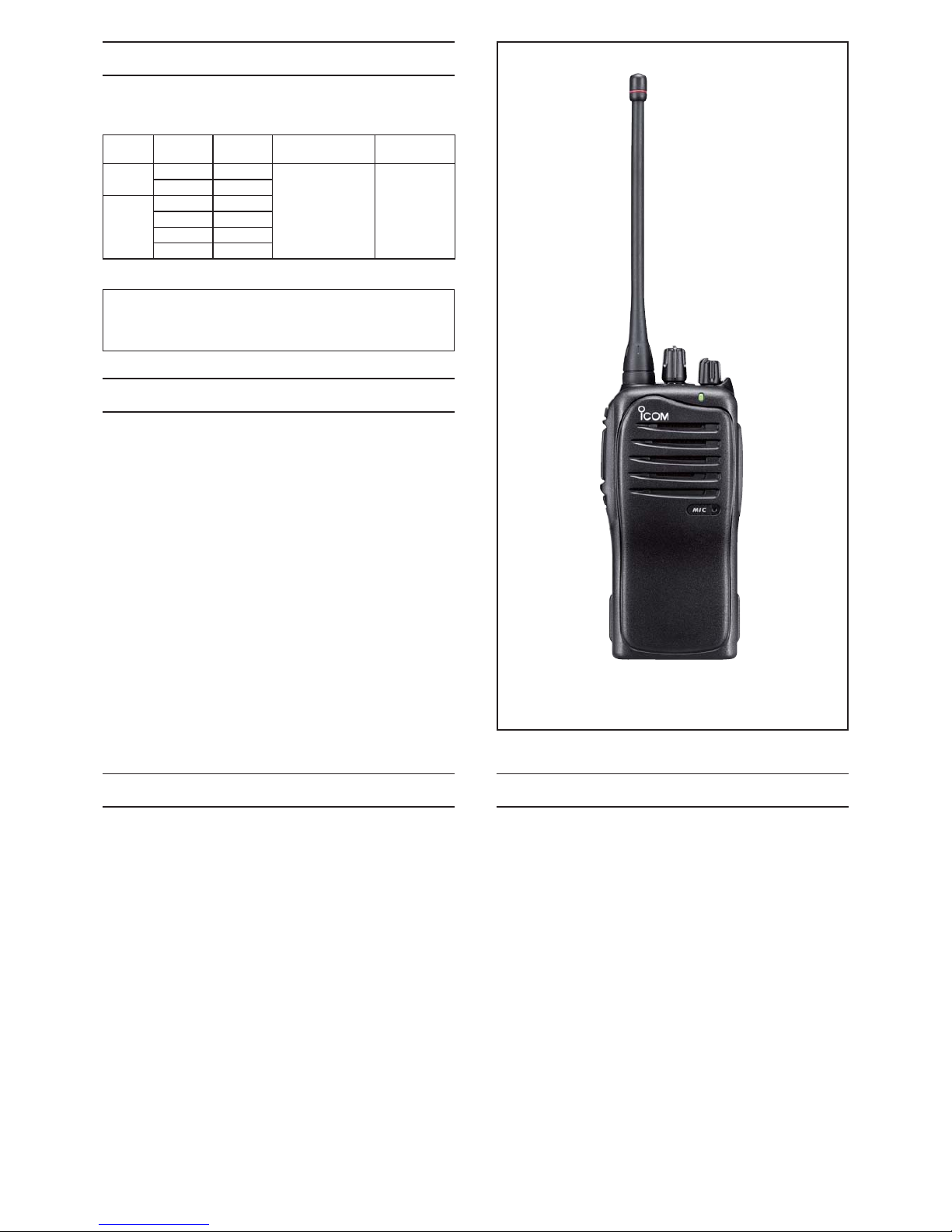
(IC-F4011)
MODEL VERSION
FREQ.
(MHz)
CHANNEL
SPACING
CHANNELS
F4011
USA-06 400–470
12.5/25.0 kHz 16CH
USA-07 450–512
F4013
CSA-01 400–470
CSA-02 450–512
CSA-03 400–470
CSA-04 450–512

TABLE OF CONTENTS
SECTION 1 SPECIFICATIONS
SECTION 2 INSIDE VIEWS
SECTION 3 DISASSEMBLY INSTRUCTION
SECTION 4 CIRCUIT DESCRIPITON
4-1 RECEIVER CIRCUITS. . . . . . . . . . . . . . . . . . . . . . . . . . . . . . . . . . . . . . . . . . . . . . . . . . . . . . . . 4-1
4-2 TRANSMITTER CIRCUITS . . . . . . . . . . . . . . . . . . . . . . . . . . . . . . . . . . . . . . . . . . . . . . . . . . . . 4-2
4-3 PLL CIRCUITS. . . . . . . . . . . . . . . . . . . . . . . . . . . . . . . . . . . . . . . . . . . . . . . . . . . . . . . . . . . . . . 4-4
4-4 OTHER CIRCUITS . . . . . . . . . . . . . . . . . . . . . . . . . . . . . . . . . . . . . . . . . . . . . . . . . . . . . . . . . . 4-5
4-5 POWER SUPPLY CIRCUITS. . . . . . . . . . . . . . . . . . . . . . . . . . . . . . . . . . . . . . . . . . . . . . . . . . . 4-5
4-6 PORT ALLOCATIONS . . . . . . . . . . . . . . . . . . . . . . . . . . . . . . . . . . . . . . . . . . . . . . . . . . . . . . . . 4-5
SECTION 5 ADJUSTMENT PROCEDURES
5-1 PREPARATION . . . . . . . . . . . . . . . . . . . . . . . . . . . . . . . . . . . . . . . . . . . . . . . . . . . . . . . . . . . . . 5-1
5-2 FREQUENCY ADJUSTMENTS. . . . . . . . . . . . . . . . . . . . . . . . . . . . . . . . . . . . . . . . . . . . . . . . . 5-6
5-3 TRANSMIT ADJUSTMENTS . . . . . . . . . . . . . . . . . . . . . . . . . . . . . . . . . . . . . . . . . . . . . . . . . . . 5-8
5-4 RECEIVERY ADJUSTMENTS. . . . . . . . . . . . . . . . . . . . . . . . . . . . . . . . . . . . . . . . . . . . . . . . . . 5-10
SECTION 6 PARTS LIST
SECTION 7 MECHANICAL PARTS
SECTION 8 BOARD LAYOUTS
SECTION 9 BLOCK DIAGRAM
SECTION 10 VOLTAGE DIAGRAM
1 - 1
SECTION 1. SPECIFICATIONS
P GENERAL
• Frequency coverage : 400–470 MHz [USA-06], [CSA-01], [CSA-03]
450–512 MHz [USA-07], [CSA-02], [CSA-04]
• Type of emission : 16K0F3E (25.0 kHz) for Wide
: 11K0F3E (12.5 kHz) for Narrow
• Channel spacing : 12.5/25.0 kHz
• Number of conventional channels : 16 ch
• Antenna impedance : 50 Ω
• Operating temperature range : –30˚C to +60˚C (–22˚F to +140˚F)
• Power supply requirement : Specified Icom's battery pack only (7.2 V DC nominal; negative ground)
• Current drain (at 7.2 V DC ; approx.) :
RECEIVING TRANSMITTING
Stand-by Max. audio
High (at 4 W) Low (at 1 W)
75 mA 300 mA 1.6 A 0.8 A
• Dimensions (projections not included) : 53.0 (W)×120.0 (H)×38.0 (D) mm; 2
3
⁄32(W)×423⁄32(H)×11⁄2(D) in
• Weight (Including BP-231) : Approx. 260 g (9
3
⁄16 oz)
P
TRANSMITTER
• Output power (at 7.2 V DC) : 4 W (Hi)/2 W (L2)/1 W (L1)
• Modulation : Variable reactance frequency modulation
• Maximum permissible deviation : ±5.0 kHz (Wide), ±2.5 kHz (Narrow)
• Frequency error : ±2.5 ppm
• Spurious emissions : 70 dB (min.)
• Adjacent channel power : 70 dB min. (75dB typ.) for Wide
60 dB min. (68dB typ.) for Narrow
• Audio harmonic distortion : 3% typ. (at 1 kHz, 40% deviation)
• FM Hum and Noise
(without CCITT filter)
: 40 dB min. (46 dB typ.) for Wide
34 dB min. (40 dB typ.) for Narrow
• Limiting charact of modulator : 60–100% of maximum deviation
• Microphone impedance : 2.2 k
Ω
P
RECEIVER
• Receive system : Double conversion superheterodyne system
• Intermediate frequencies : 1st IF: 46.35 MHz, 2nd IF: 450 kHz
• Sensitivity : 0.25 µV (–119 dBm) typ. at 12 dB SINAD
• Adjacent channel selectivity : 70 dB min. (75 dB typ.) for Wide
60 dB min. (65 dB typ.) for Narrow
• Spurious response : 70 dB min.
• Intermodulation rejection ratio : 70 dB min. (74 dB typ.)
• Hum and Noise (without CCITT filter) : 40 dB min. (45 dB typ.) for Wide
34 dB min. (40 dB typ.) for Narrow
• Audio output power : 0.5 W typ. (at 5% distortion with an 8 Ω load)
• Squelch sensitivity (at threshold) : 0.25 µV typ.
• Output impedance (audio) : 8
Ω
Specifications are measured in accordance with TIA-603.
All stated specifications are subject to change without notice or obligation.
2 - 1
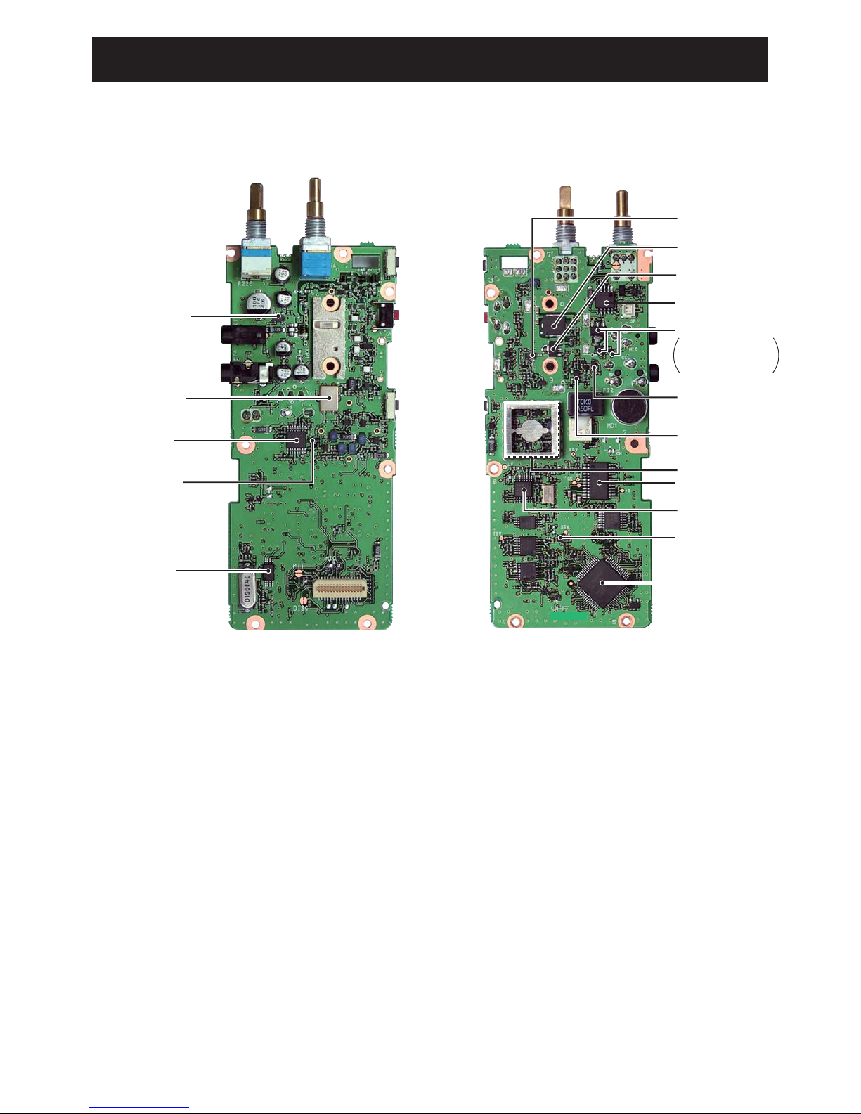
SECTION 2. INSIDE VIEWS
+5 Regulator
(IC9: NJM2870F05)
AF amplifier
(IC12: TA7368F)
D/A converter
(IC8: M62363FP)
R5 Regulator
(Q22: 2SA1577)
CPU
(IC13: HD6433687A91
F
S5 Regulator
Q23: 2SB1132
Q24: XP6501
Q25: UNR9113G0L
Crystal filter
(FI1: FL-335)
FM IF IC
(IC1: TA31136FNG)
IF amplifier
(Q4: 2SC4215)
EEPROM
(IC15: BR24L16FV)
Power amplifier
(Q7: RD07MVS2)
T5 Regulator
(Q21: 2SA1577)
PLL IC
(IC4: MB15A02PFV1)
Pre-drive
(Q5: 2SC3356)
APC amplifier
(IC2: TC75S51F)
VCO circuit
TOP VIEW BOTTOM VIEW
• MAIN UNIT
Drive amplifier
(Q8: RD01MUS2)
3 - 1
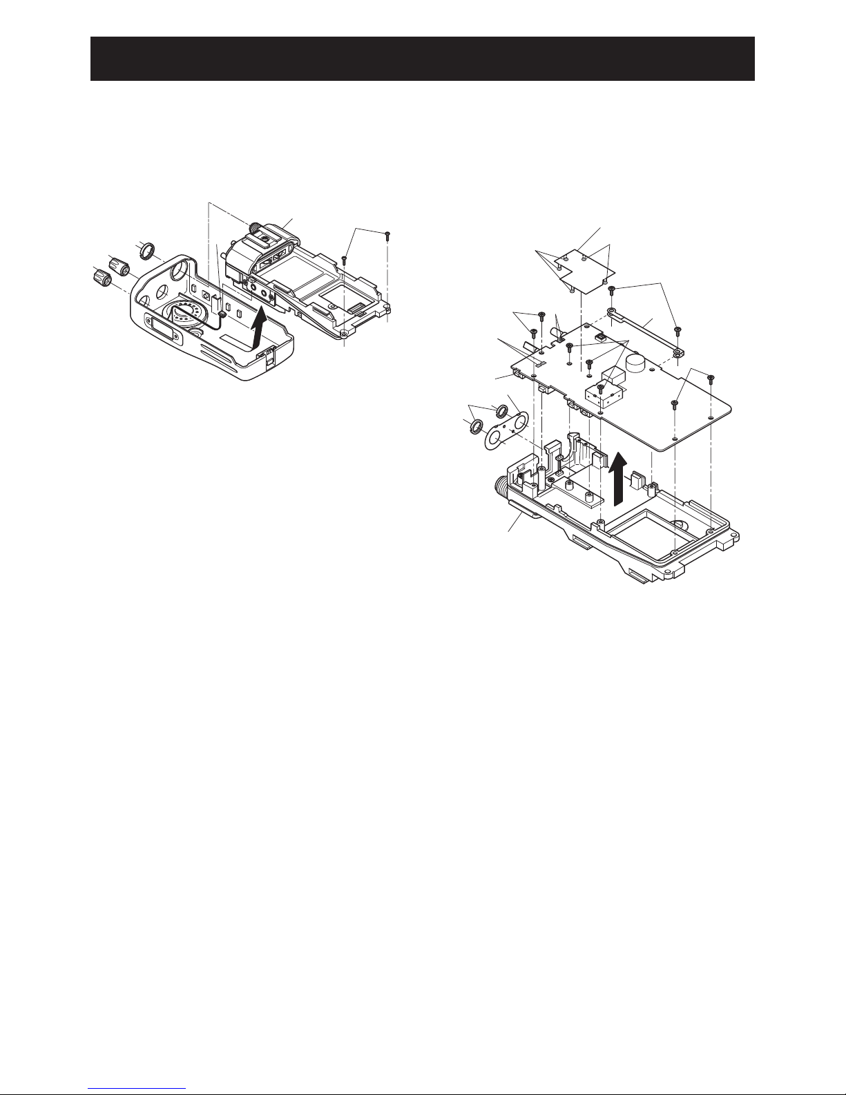
SECTION 3. DISASSEMBLY INSTRUCTION
1. REMOVING THE CHASSIS UNIT
q Unscrew 1 nut A, and remove 2 knobs B, C.
w Unscrew 2 screws D.
e Take off the chassis unit in the direction of the arrow.
r Unplug the connector E from the chassis unit.
2. REMOVING THE MAIN UNIT
q Unscrew 2 nuts F, and remove the top plate G.
w Unsolder 5 points H, and remove the shield cover.
e Unscrew 2 screws I, and remove the side plate J.
r Unscrew 7 screws K.
t Unsolder 4 points L, and take off the main unit in the
direction of the arrow.
Chassis unit
D
A
B
C
E
Main unit
I
K
K
L
K
F
G
Chassis unit
L
H
H
J
Shield cover
4 - 1
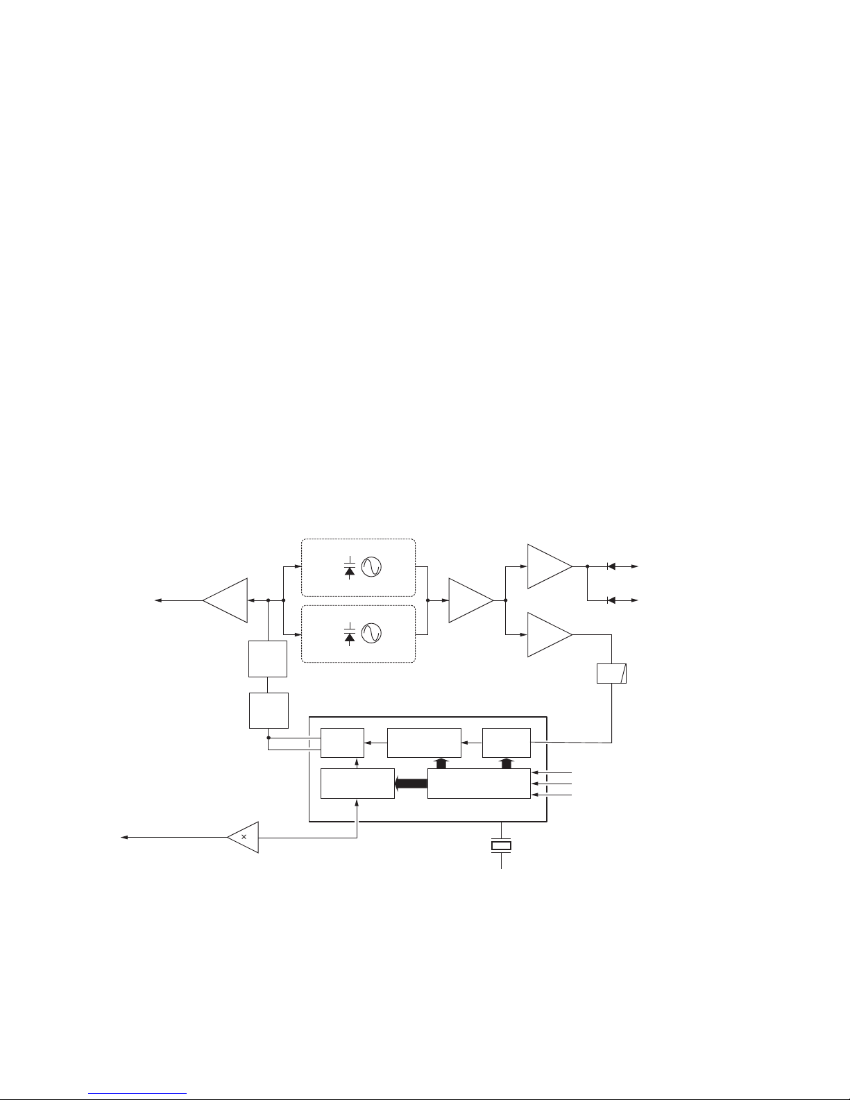
SECTION 4. CIRCUIT DESCRIPTION
4-1 RECEIVER CIRCUITS
4-1-1 ANTENNA SWITCHING CIRCUIT
The antenna switching circuit functions as a low-pass filter
while receiving and a resonator circuit while transmitting.
This circuit does not allow transmit signals to enter the
receiver circuits.
Received signals enter the antenna connector (CHASSIS;
J1) and pass through the low-pass filters (ANT UNIT; L601,
C601) and (MAIN UNIT; L1, L2, L45, C1–C6, C175). The
filtered signals are passed through the 1⁄4
λ type antenna
switching circuit (D2, D5, L6) and then applied to the RF circuit.
4-1-2 RF CIRCUIT
The RF circuit amplifies signals within the range of frequency coverage and filters out-of-band signals.
The signals from the antenna switching circuit pass through
the bandpass filter (D3, D4, D7, D8). The filtered signals are
amplified at the RF amplifier (Q2) and then passed through
the another bandpass filter (D9, D10, C38–C40, C44, C45)
to suppress unwanted signals. The filtered signals are
applied to the 1st mixer circuit.
D3, D4, D7–D10 employ varactor diodes, that are controlled by the CPU via the D/A converter (IC8), to track
the bandpass filter. These varactor diodes tune the center
frequency of an RF passband for wide bandwidth receiving
and good image response rejection.
4-1-3 1ST MIXER AND 1ST IF CIRCUITS
The 1st mixer circuit converts the received signal into fixed
frequency of the 1st IF signal with the PLL output frequency.
By changing the PLL frequency, only the desired frequency
passes through a crystal filter at the next stage of the 1st
mixer.
The RF signals from the bandpass filter are mixed with the
1st LO signals, where come from the RX VCO circuit via the
BPF (L38, C49, C304, C305), at the 1st mixer circuit (Q3)
to produce a 46.35 MHz 1st IF signal. The 1st IF signal is
passed through a monolithic filter (FI1) in order to obtain
selection capability and to pass only the desired signal.
The filtered signal is applied to the 2nd IF circuit after being
amplified at the 1st IF amplifier (Q4).
4-1-4 2ND IF AND DEMODULATOR CIRCUITS
The 2nd mixer circuit converts the 1st IF signal into a 2nd
IF signal. The double-conversion superheterodyne system
(which converts receive signals twice) improves the image
rejection ratio and obtains stable receiver gain.
The 1st IF signal from the IF amplifier (Q4) is applied to
the 2nd mixer section of the FM IF IC (IC1, pin 16), and
is mixed with the 2nd LO signal to be converted into a
450 kHz 2nd IF signal.
The FM IF IC (IC1) contains the 2nd mixer, 2nd local oscillator, limiter amplifier, quadrature detector, active filter and
noise amplifier circuits. A 2nd LO signal (45.9 MHz) is produced at the PLL circuit by tripling it’s reference frequency
(15.3 MHz).
The 2nd IF signal from the 2nd mixer (IC1, pin 3) passes
through the ceramic filter (FI2) to remove unwanted heterodyned frequencies. It is then amplified at the limiter amplifier
section (IC1, pin 5) and applied to the quadrature detector
section (IC1, pins 10, 11) to demodulate the 2nd IF signal
into AF signals.
The demodulated AF signals are output from pin 9 (IC1) as
“DET” signal, and are then applied to the AF circuit.
Mixer
16
Limiter
AMP
2nd IF filter
450 kHz
X2
15.3 MHz
45.9 MHz
IC1 TA31136FN
12
1st IF signal from the IF amplifier (Q4)
"RSSI" signal to the CPU (IC13, pin 63)
11109
87
5
AF signal "DET"
to the AF circuit
"SQLC" signal from the
D/A converter IC
(IC8, pin 2)
To D/A converter IC
(IC8, pin 1)
R5V
X1
2
Active
filter
Noise
detector
FM
detector
13
"NOIS" signal to the CPU (IC13, pin 53)
RSSI
Noise
AMP
Noise
comparator
×3
Q19
FI2
3
• 2ND IF AND DEMODULATOR CIRCUITS
4 - 2
4-1-5 AF AMPLIFIER CIRCUIT
The AF amplifier circuit amplifies the demodulated AF signals to drive a speaker.
The AF signals from the FM IF IC (IC1, pin 9) pass through
the high-pass filter (IC6, pins 3 and 1) to suppress unwanted harmonic components. The signals pass through the
RX mute switch (Q34) which is controlled by “RMUT” signal from the CPU (IC13, pin 56), and are then applied to
another high-pass filter (IC6, pins 13 and 14). The filtered
signals pass through the low-pass filter (IC6, pins 6 and 7)
via the analog switch (IC10, pins 1 and 2). The signals are
applied to the analog switch (IC10, pin 10) again, and are
then applied to the AF power amplifier (IC12, pin 4) via the
AF volume (R226). The amplified AF signals are output from
pin 10, and are then applied to the internal speaker which is
connected with J1 via the [SP] jack.
4-1-6 RECEIVE MUTE CIRCUITS
• NOISE SQUELCH
A squelch circuit cuts out AF signals when no RF signals
are received. By detecting noise components in the AF signals, the squelch circuit switches the AF mute switch.
Some noise components in the AF signals from the FM IF
IC (IC1, pin 9) are applied to the D/A converter (IC8, pin 1)
as “DET” signal, and are then output from pin 2. The signals
are applied to the active filter section in the FM IF IC (IC1,
pin 8). The active filter section filters and amplifies noise
components. The amplified signals are converted into the
pulse-type signals at the noise detector section and output
from pin 13 as “NOIS” signal.
The “NOIS” signal from the FM IF IC is applied to the CPU
(IC13, pin 53). Then the CPU analyzes the noise condition
and outputs the AF mute control signal from the CPU (IC13)
as “RMUT” signal from pin 56. The signal is applied to the
RX mute switch (Q34) to control the AF signal muting.
• CTCSS AND DTCS
The tone squelch circuit detects tone signals and opens the
squelch only when receiving a signal containing a matched
subaudible tone (CTCSS or DTCS). When the tone squelch
is in use, and a signal with a mismatched or no subaudible
tone is received, the tone squelch circuit mutes the AF signals even when noise squelch is open.
A portion of the “DET” signals from the FM IF IC (IC1,
pin 9) passes through the low-pass filter (IC7, pins 5 and 7)
to remove AF (voice) signals, and are then applied to the
amplifier (IC7, pin 3). The amplified signals are applied to
the CTCSS or DTCS decoder inside of the CPU (IC13,
pin 60) as the “CDEC” signal. The CPU outputs AF mute
control signal from pin 56, and is then applied to the RX
mute switch (Q34) and analog switch (IC10, pins 12 and 13)
to control AF signals muting as “RMUT” signal.
4-2 TRANSMITTER CIRCUITS
4-2-1 MICROPHONE AMPLIFIER CIRCUIT
The microphone amplifier circuit amplifies audio signals
within +6 dB/octave pre-emphasis characteristics from the
microphone to a level needed for the modulation circuit.
The AF signals from the microphone are passed through
the microphone mute switch (Q35), and are then applied
to the amplifier (IC6, pins 9 and 8) via the high-pass filter
(IC6, pins 13 and 14). The amplified signals are applied to
the analog switch (IC10, pin 4), and outputs from pin 3. The
signals pass through the low-pass filter (IC6, pins 6 and 7),
then applied to the analog switch (IC10, pin 9) again and
output from pin 8.
The signals are applied to the D/A converter (IC8, pin 4).
The converted signals output from pin 3, and applied to the
modulation circuit (D18) as “MOD” signal.
Analog SW
(IC10)
"DET" AF signal
from FM IF IC (IC1, pin 9)
8
AF
volume
AF
AMP
MIC
MUTE
IC12
Q35
Speaker
R226
IC8
D18
RX
MUTE
Q34
LPF
IC6 B
HPF
IC6 D
HPF
IC6 A
Microphone
IC6 C
AMP
1
4
3
2
9
10
D/A converter
FM mod.
"CTCSS/DTCS" signal from
D/A conveter IC (IC8, pin 10)
"TONE" signal from CPU (IC13) via low-pass
filters (IC5 A / IC5 B pin 7)
to TX VCO circuit
(Q13, D16, D17)
11
• ANALOG SWITCHING CIRCUITS
4 - 3
4-2-2 MODULATION CIRCUIT
The modulation circuit modulates the VCO oscillating signal
(RF signal) using the audio signals from the microphone.
The AF signals from the D/A converter (IC8, pin 3) change
the reactance of varactor diode (D18) to modulate the oscillated signal at the TX VCO circuit (Q13, D17, D18, D21).
The modulated VCO signal is amplified at the buffer amplifiers (Q10, Q12) and then applied to the drive amplifier circuit
via the T/R switch (D14, D15).
The CTCSS/DTCS signals (“CENC0”, “CENC1”, ”CENC2”)
from the CPU (IC13, pins 23–25) pass through the low-pass
filter (IC5, pins 12 and 14) via 3 registers (R191–R193) to
change its wave form. Then the signals are applied to the
D/A converter (IC8, pin 9). The output signals from the D/
A converter (IC8, pin 10) pass through the low-pass filter
(IC6, pins 6 and 7) to be mixed with “MOD” signal, and then
applied to the D/A converter again (IC8, pin 4).
4-2-3 DRIVE/POWER AMPLIFIER CIRCUITS
The drive/power amplifier circuits amplify the VCO oscillating signal to a transmit power level.
The modulated RF signal from the TX VCO circuit passes
through the T/R switch (D14, D15) and is amplified at the
YGR (Q9), pre-drive (Q5), drive (Q8), and power (Q7)
amplifiers to obtain 4 W of RF power (at 7.2 V DC).
The amplified signal passes through the low-pass filter (L1,
L2, L45, C1–C5, C175, C176), antenna switch (D2) and
power detector (D1, D30), then applied to the antenna connector (CHASSIS unit; J1).
4-2-4 APC CIRCUITS
The bias current of the drive (Q8) and power (Q7) amplifiers
are controlled by the APC circuit.
The APC circuit (IC2, D1, D30) protects drive and power
amplifiers from the reflected signal, and selects output
power of HIGH, LOW2 or LOW1.
The power detector (D1, D30) detects transmit output power
and converts it into DC voltage. The DC voltage is at a minimum level when the antenna impedance is matched to 50 Ω,
and increased when mismatched.
The detected voltage is applied to the differential amplifier
(IC2, pin 3), and the “T2” signal from the D/A converter (IC8,
pin 23), controlled by the CPU (IC13), is applied to pin 1 for
reference. When antenna impedance is mismatched, the
detected voltage exceeds the power setting voltage. Then
the output voltage of the differential amplifier (IC2, pin 4)
controls the input current of the drive (Q8), and power (Q7)
amplifiers to reduce the output power.
Powe r
AMP
Differential
AMP
Driver
AMP
+
–
VCC
to ANT unit
T2
TMUT
RF signal
from Buffer AMP
T5V
D1
YGR
AMP
ANT
SW
LPF
LPF
Q8
IC2
Q9
Q7
D2
• APC CIRCUITS
4 - 4
4-3 PLL CIRCUITS
4-3-1 PLL CIRCUIT
A PLL circuit provides stable oscillation for the transmit frequency and the receive 1st LO frequency. The PLL output
compares the phase of the divided VCO frequency to the
reference frequency. The PLL output frequency is controlled
by the divided ratio (N-data) of a programmable divider.
The PLL circuit contains the TX/RX VCO circuits (TX:
Q13, D17, D21; RX: Q14, D16, D21). The oscillated signal is amplified at the buffer amplifiers (Q11, Q12) and
then applied to the PLL IC (IC4, pin 8) after being passed
through the low-pass filter (L32, C206, C208).
The phase detected signal is output from pins 15 and 16,
and passes through the loop filter (C130, C138, C146,
C147, R95–R97), then applied to the TX and RX VCO circuits as a lock voltage.
The PLL IC contains a prescaler, programmable counter,
programmable divider and phase detector, etc. The entered
signal is divided at the prescaler and programmable counter
section by the N-data ratio from the CPU. The divided signal
is detected on phase at the phase detector using the reference frequency.
If the oscillated signal drifts, its phase changes from that of
the reference frequency, causing a lock voltage change to
compensate for the drift in the oscillated frequency.
4-3-2 VCO CIRCUITS
The VCO circuit contains a separate RX VCO (Q14, D16,
D22) and TX VCO (Q13, D17, D18, D21). The oscillated
signal is amplified at the buffer amplifiers (Q10, Q12) and
is then applied to the T/R switch (D14 for TX, D15 for RX).
Then the receive 1st LO (RX) signal is applied to the 1st
mixer circuit (Q3) and the transmit (TX) signal to the preYGR amplifier (Q9).
A portion of the signal from the buffer amplifier (Q12) is fed
back to the PLL IC (IC4, pin 8) via the buffer amplifier (Q11)
and low-pass filter (L32, C206, C208) as the comparison
signal.
Shift register
Prescaler
Phase
detector
Loop
filter
Programmable
counter
Programmable
divider
X2
15.3 MHz
2
Buffer
Q12
Buffer
Q18
Buffer
Q10
Buffer
Q11
14
15
16
SCK
SO
PLST
to transmitter circuit
to 1st mixer circuit
D14
D15
1
15
16
8
Q13, D16, D17, D21
TX VCO
Q14, D19, D20, D22
RX VCO
IC4 MB15A02
3
45.9 MHz 2nd LO
signal to the FM IF IC
(IC1, pin 2)
Tripler
Q19
"LVIN" signal to the CPU
(IC13, pin 64)
LPF
Charge
Pump
Q39, Q40
• PLL CIRCUITS
 Loading...