

Page 1
S-14617XZ-C1
Nov. 2009
UHF TRANSCEIVERS
Page 2
This service manual describes the latest technical
information for the IC-F4001/IC-F4002/IC-F4003/IC-F4006/
IC-F4008 UHF TRANSCEIVERS at the time of publication.
NEVER connect the transceiver to an AC outlet or to a DC
power supply that uses more than the specified voltage.
This will ruin the transceiver.
DO NOT expose the transceiver to rain, snow or any liquids.
DO NOT reverse the polarities of the power supply when
connecting the transceiver.
DO NOT apply an RF signal of more than 20 dBm (100 mW) to
the antenna connector. This could damage the transceiver’s
front-end.
To upgrade quality, any electrical or mechanical parts
and internal circuits are subject to change without notice
or obligation.
MODEL VERSION
CHANNEL
SPACING
(kHz)
FREQUENCY
RANGE
(MHz)
IC-F4001
USA-11
12.5/25.0
400–470
USA-12
USA-13
IC-F4002
EUR-21
12.5/20.0/25.0EUR-22
EUR-23
UK-01
12.5/25.0
UK-02
UK-03
IC-F4003
EXP-11
EXP-12
EXP-13
EXP-21
EXP-22
EXP-23
EXP-01
EXP-03
EXP-31
AUS-21
AUS-22
AUS-23
IC-F4006
RUS-21
RUS-22
RUS-23
IC-F4008 CHN-31
Be sure to include the following four points when ordering
replacement parts:
1. 10-digit Icom part number
2. Component name
3. Equipment model name and unit name
4. Quantity required
<ORDER EXAMPLE>
1110003491 S.IC TA31136FNG IC-F4001 MAIN UNIT 5 pieces
8820001210 Screw 2438 screw IC-F4003 Top cover 10 pieces
Addresses are provided on the inside back cover for your
convenience.
ORDERING PARTS
1. Make sure that the problem is internal before
disassembling the transceiver.
2. DO NOT open the transceiver until the transceiver is
disconnected from its power source.
3. DO NOT force any of the variable components. Turn
them slowly and smoothly.
4. DO NOT short any circuits or electronic parts. An
insulated tuning tool MUST be used for all adjustments.
5. DO NOT keep power ON for a long time when the
transceiver is defective.
6. DO NOT transmit power into a Standard Signal
Generator or a Sweep Generator.
7. ALWAYS connect a 50 dB to 60 dB attenuator between
the transceiver and a Deviation Meter or Spectrum
Analyzer when using such test equipment.
8. READ the instructions of the test equipment throughly
before connecting it to the transceiver.
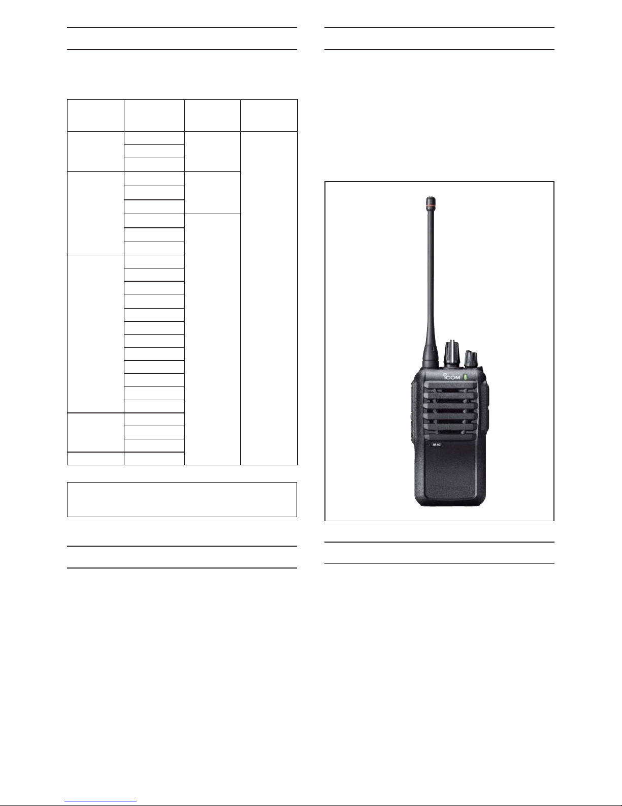
REPAIR NOTES
INTRODUCTION CAUTION
(IC-F4001)
Icom, Icom Inc. and the Icom logo are registered trademarks of Icom Incorporated (Japan) in Japan, the United States, the
United Kingdom, Germany, France, Spain, Russia and/or other countries.
Page 3

TABLE OF CONTENTS
SECTION 1 SPECIFICATIONS
SECTION 2 INSIDE VIEWS
SECTION 3 DISASSEMBLY INSTRUCTION
SECTION 4 CIRCUIT DESCRIPITON
4-1 RECEIVER CIRCUITS. . . . . . . . . . . . . . . . . . . . . . . . . . . . . . . . . . . . . . . . . . . . . . . . . . . . . . . . 4-1
4-2 TRANSMITTER CIRCUITS . . . . . . . . . . . . . . . . . . . . . . . . . . . . . . . . . . . . . . . . . . . . . . . . . . . . 4-2
4-3 FREQUENCY SYNTHESIZER CIRCUITS . . . . . . . . . . . . . . . . . . . . . . . . . . . . . . . . . . . . . . . . 4-3
4-4 VOLTAGE BLOCK DIAGRAM . . . . . . . . . . . . . . . . . . . . . . . . . . . . . . . . . . . . . . . . . . . . . . . . . . 4-3
4-5 PORT ALLOCATIONS . . . . . . . . . . . . . . . . . . . . . . . . . . . . . . . . . . . . . . . . . . . . . . . . . . . . . . . . 4-4
SECTION 5 ADJUSTMENT PROCEDURES
5-1 PREPARATION . . . . . . . . . . . . . . . . . . . . . . . . . . . . . . . . . . . . . . . . . . . . . . . . . . . . . . . . . . . . . 5-1
5-2 FREQUENCY ADJUSTMENT . . . . . . . . . . . . . . . . . . . . . . . . . . . . . . . . . . . . . . . . . . . . . . . . . . 5-5
5-3 TRANSMIT ADJUSTMENT . . . . . . . . . . . . . . . . . . . . . . . . . . . . . . . . . . . . . . . . . . . . . . . . . . . . 5-6
5-4 RECEIVE ADJUSTMENT . . . . . . . . . . . . . . . . . . . . . . . . . . . . . . . . . . . . . . . . . . . . . . . . . . . . . 5-7
SECTION 6 PARTS LIST
SECTION 7 MECHANICAL PARTS
SECTION 8 BOARD LAYOUTS
SECTION 9 BLOCK DIAGRAM
SECTION 10 VOLTAGE DIAGRAM
Page 4

1 - 1
SECTION 1. SPECIFICATIONS
M GENERAL
• Frequency range : 400–470 MHz
• Number of conventional channels : 16 channels
• Type of emission : [EUR] Wide: 16K0F3E (25.0 kHz)
Middle: 14K0F3E (20.0 kHz)
Narrow: 8K50F3E (12.5 kHz)
Except [EUR] Wide: 16K0F3E (25.0 kHz)
Narrow: 11K0F3E (12.5 kHz)
• Antenna impedance : 50 Ω (Nominal)
• Operating temperature range : –30˚C to +60˚C; –22˚F to +140˚F Except [EUR], [UK]
–25˚C to +55˚C [EUR], [UK]
• Power supply voltage : Specified Icom's battery packs only (7.2 V DC; negative ground)
• Current drain (Approx.) : Receiving 70 mA (stand-by)
330 mA (max. audio)
Transmitting 1.3 A (at 4.0 W)
• Dimensions
(Projections not included)
: With BP-264
58.6 (W)×111.0 (H)×31.0 (D) mm; 2 5/16 (W)×4 3⁄8 (H)×1 7⁄32 (D) in.
With BP-265
58.6 (W)×111.0 (H)×35.5 (D) mm; 2 5/16 (W)×4 3⁄8 (H)×1 13⁄32 (D) in.
• Weight : With BP-264 Approx. 330 g; 11 21/32 oz.
With BP-265 Approx. 270 g; 9 17/32 oz.
• Intermediate frequency : 1st 46.35 MHz
2nd 450 kHz
• Output impedance (Audio) : 8
Ω
• Input impedance (Audio) : 2.2 k
Ω
M TRANSMITTER
• Output power : 4 W
• Modulation : Variable reactance frequency modulation
• Maximum frequency deviation : Narrow ±2.5 kHz
Middle ±4.0 kHz
Wide ±5.0 kHz
• Frequency stability : ±2.5 ppm
• Spurious emissions : 70 dB min. Except [EUR], [UK]
0.25 µW (≤1 GHz), 1.0 µW (>1 GHz) [EUR], [UK]
• Adjacent channel power : Narrow 60 dB min., 66 dB typ.
Middle
70 dB min., 73 dB typ.
Wide 70 dB min., 73 dB typ.
• Audio harmonic distortion : Wide, Middle 1.0% typ. at AF 1 kHz 40 % deviation
Narrow 1.5% typ. at AF 1 kHz 40 % Deviation
• FM hum and Noise
(Except [EUR], [UK])
(Without CCITT FILTER)
: Narrow 34 dB min., 40 dB typ.
Wide 40 dB min., 46 dB typ.
• Residual modulation ([EUR], [UK])
(With CCITT FILTER)
: Narrow 40 dB min.
Middle 43 dB min.
Wide 45 dB min.
• Limitting charact of modulator : 60–100% of max. deviation
Page 5

1 - 2
M RECEIVER
• Sensitivity : 0.25 µV typ. at 12 dB SINAD Except [EUR], [UK]
–4 dBµV (EMF) typ. at 20 dB SINAD [EUR], [UK]
• Squelch sensitivity (at threshold) : 0.25 µV typ. Except [EUR], [UK]
–4 dBµV (EMF) typ. [EUR], [UK]
• Intermodulation : 70 dB min. 74 dB typ. Except [EUR], [UK]
65 dB min. [EUR], [UK]
• Spurious response : 70 dB min.
• Audio output power : 0.8 W typ. at 5% distortion with 12 Ω (Int. speaker)
0.4 W typ. at 5% distortion with 8 Ω (Ext. speaker)
• Hum and noise (Except [EUR], [UK])
(Without CCITT Filter)
: Narrow 34 dB min. 47 dB typ.
Wide 40 dB min. 52 dB typ.
• Hum and noise (
[
EUR], [UK])
(With CCITT Filter)
: Narrow
40 dB min.
Middle
43 dB min.
Wide
45 dB min.
• Adjacent channel selectivity : Narrow 60 dB min. 65 dB typ.
Middle 70 dB min. 73 dB typ.
Wide 70 dB min. 73 dB typ.
Specifications are measured in accordance with TIA/EIA-603B or EN 300 086
All stated specifications are subject to change without notice or obligation.
Page 6
2 - 1
SECTION 2. INSIDE VIEWS
LED CTRL
(Q82,Q83)
VCO
• MAIN-A UNIT
(TOP VIEW)
CPU5 LINE REGULATOR
(IC54)
+5V LINE REGULATOR
(Q76)
PLL IC
(IC2)
MIC/AF LINE SW
(IC56)
APC AMP
(IC1)
TCXO
(X2)
TONE FILTER SW
(Q52)
TONE LPF
(IC59)
HPF
(IC58)
MIC GAIN CONTROLLER
(IC62)
2ND IF BPF
(FI2)
2ND IF BPF (
For narrow mode only
)
(FI3)
LPF
(Q51)
BEEP SW
(IC61)
+5V LINE REGULATOR
(Q75)
Page 7
2 - 2
CLONE BUFFER
(Q81, D51)
TUNED BPF
(D24, D26)
• MAIN-A UNIT
(BOTTOM VIEW)
DRIVE AMP
(Q2)
POWER AMP
(Q1)
PRE-DRIVE AMP
(Q3)
PRE-AMP
(Q4)
RF AMP
(Q22)
RESET IC
(IC53)
EEPROM
(IC52)
AF AMP
(IC55)
IF DEMODULATOR IC
(IC3)
XTAL BPF
(FI1)
AGC CTRL
(Q21)
S5 LINE REGULATOR
(Q71)
RIPPLE FILTER
(Q15)
R5 LINE REGULATOR
(Q72)
1ST IF MIXER
(Q23)
POWER CTRL
(Q63)
CPU
(IC51)
D/A CONVERTER
(IC57)
BUFFER
(IC60)
BUFFER
(Q9)
+5V LINE REGULATOR
(Q74)
Page 8
3 - 1
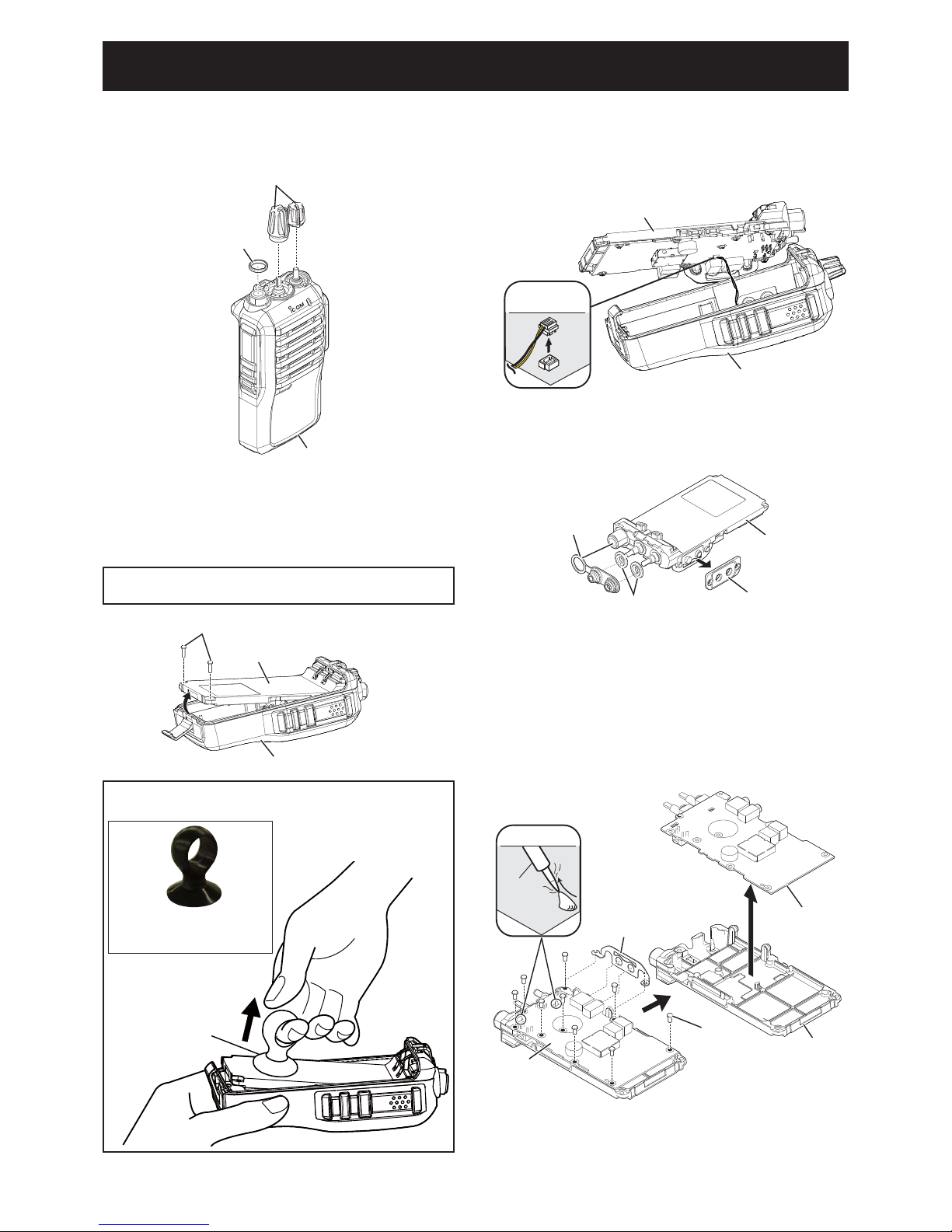
SECTION 3. DISASSEMBLY INSTRUCTION
BE CAREFUL to not pull out the speaker wire when
separating the CHASSIS and the FRONT PANEL.
For easy separation of the CHASSIS
Use a suction lifter to lift the bottom of the CHASSIS up.
1. REMOVING THE CHASSIS
1) Remove the ANT connector nut and 2 knobs.
2. REMOVING THE MAIN UNIT
1) Remove the 9 screws and the side plate from the
MAIN UNIT.
2) Unsolder the 2 points shown, and then remove the
MAIN UNIT.
2) Remove 2 screws from the bottom of the CHASSIS.
3) Lift the bottom of the CHASSIS up in the direction
of the arrow.
4)
CAREFULLY lift the chassis out of the FRONT PANEL
and turn it over in order to unplug the speaker wire.
(Continued to the right above)
5) Remove the seals and nuts from the CHASSIS.
ANT CONNECTOR NUT
KNOBS
FRONT PANEL
FRONT PANEL
CHASSIS
SCREWS×2
SPEAKER
WIRE
CHASSIS
FRONT PANEL
TOP SEAL
NUTS×2
SIDE SEAL
CHASSIS
UNSOLDER
Solder
remover
CHASSIS
SCREWS×9
MAIN UNIT
MAIN UNIT
SIDE PLATE
Suction lifter
Suction lifter
• Part name : EA950R-2
• Manufacture : ESCO CO.LTD
Page 9
4 - 1
• RF CIRCUITS
• 1ST IF CIRCUITS
• 2ND IF CIRCUITS
SECTION 4. CIRCUIT DESCRIPTION
LPF
ANT
SW
D3,D22
RF
AMP
Q22
BPF
D28 D24,D26
BPF
T2
T1
From the TX circuits
To the 1st IF circuits
ANT
LO
SW
D5,D6
Q23
BPF
XTAL
FI1
IF
AMP
Q24
BUFF
Q8
BUFF
Q10
LPF
RX VCO
To the TX circuits
From the RF circuits
To the 2nd IF&demodulator circuits
46.35MHz
1st IF mixer
PLL
IC
IC2
MB15A02
X3
Q26
BPF
X2
TCXO
W/N
SW
Q27,
D33,D34
X1
Discriminator
BPF
CERAMIC
FI2
BPF
CERAMIC
FI3
W/N
SW
D31,D32
D/A
converter
IF IC
From the 1st IF
circuits
To the RX AF circuits
IC3:NJM2591
15.3MHz
45.9MHz
DISC
SQIN
IC57
R2A20178
450kHz
450kHz
NWC
NOIS
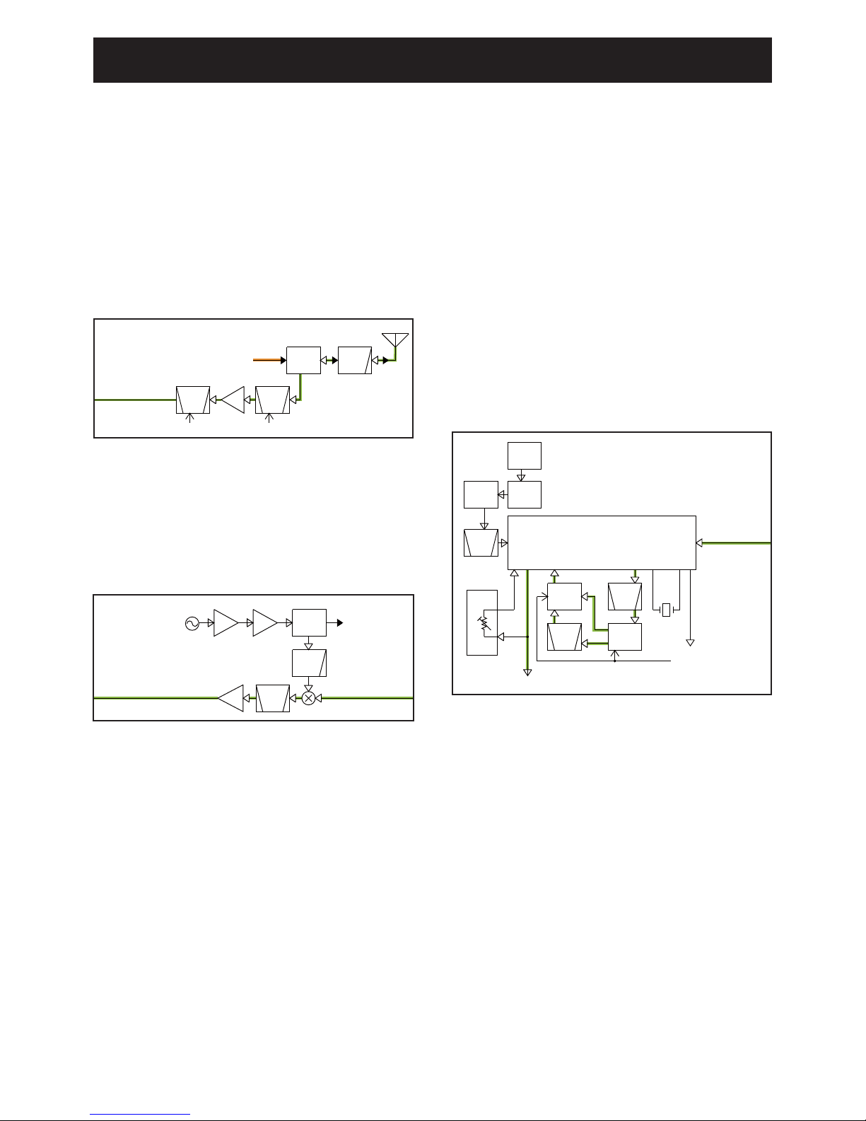
4-1 RECEIVER CIRCUITS
RF CIRCUITS
The RX signal from the antenna is passed through the LPF
and antenna SW, then filtered by the 2-staged tuned BPF
to eliminate unwanted out-of-band signal. The filtered RX
signal is amplified by the RF AMP, and filtered by another
2-staged tuned BPF to obtain a good image response, then
applied to the 1st IF circuits.
The tuned BPFs are tuned to the RX frequency by applying
adequate tuning voltages; “T1” and “T2” to the variable
capacitors.
1ST IF CIRCUITS
The RX signal from the RF circuits is applied to the 1st IF
mixer and mixed with the 1st LO signal from the RX VCO,
resulting in the 46.35 MHz 1st IF signal. The 1st IF signal is
filtered by the crystal filter, amplified by the 1st IF AMP, then
applied to the 2nd IF circuits.
2ND IF CIRCUITS AND DEMODULATOR
The signal from the 1st IF circuits is applied to the IF
demodulator IC which contains the 2nd IF mixer, 2nd IF
AMP, FM detector, etc. in its package.
The 1st IF signal is applied to the 2nd IF mixer and mixed
with the 2nd LO signal resulting in the 450 kHz 2nd IF
signal.
The 2nd LO signal is generated by tripling the 15.3 MHz
reference frequency signal oscillated by the reference
frequency oscillator (TCXO).
The converted 2nd IF signal is filtered by the crystal filter/
filters to eliminate unwanted signal, and amplified by the
2nd IF AMP, then demodulated by the detector circuit which
employs a discriminator as the phase shifter.
The demodulated AF signal is applied to the RX AF circuits.
Page 10
4 - 2
• RX AF CIRCUITS
AF
AM P
IC55 TPA0211DGN
J52
IC62
RX
MUTE
SP1
HPF
IC58
AF
AM P
IC12
TA7368F
HPF
IC58
J53
Int.speaker
Ext.speaker
1
2
LPF
IC58
LPF
IC59
the demodulator
circuits
IC56
AF line SW
CD4066
AFON
AFO
RMUT 1
D/A
converter
IC57
R2A20178
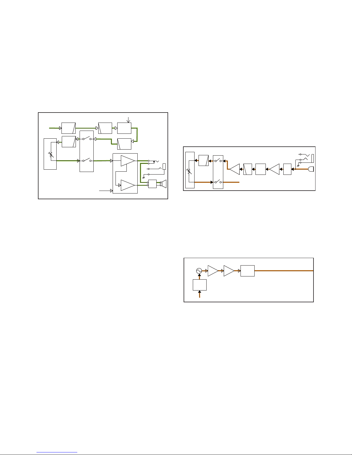
RX AF CIRCUITS
The demodulated AF signal from the IF demodulator
IC is passed through the LPF, HPF which attenuates
frequencies 300 Hz and below. The filtered AF signal is
passed through the AF line SW, HPF which additionally
attenuates frequencies 300 Hz and below, de-emphasis
circuit which provides –6 dB/oct of frequency response.
The de-emphasized AF signal is passed through the AF
SW, LPF which attenuates frequencies 3 kHz and above, is
adjusted in level by the D/A converter. The level-adjusted AF
signal is then applied to the AF power AMP via the AF line
SW.
The amplified AF signal is applied to the internal or external
speaker.
4-2 TRANSMITTER CIRCUITS
TX AF CIRCUITS
The audio signal from the internal or external microphone
(MIC signal) is passed through the MIC gain SW and applied
to the MIC AMP. The amplified MIC signal is passed through
the MIC mute SW, HPF which attenuates frequencies
300 Hz and below. The filtered MIC signal is passed through
the pre-emphasis circuit which provides +6 dB/oct of
frequency response, then they applied to the limiter AMP.
The amplitude-limited MIC signal is passed through the
MIC line SW, and applied to the splatter filter, which
attenuate harmonics in the MIC signal to prevent exceeding
permissible deviation.
The filtered MIC signal is applied to the D/A converter which
adjusts its level (=deviation). The level-adjusted MIC signal
is applied to the TX VCO as the modulation signal.
• TX AF CIRCUITS
AM
limit
P
IC58
MIC
MUTE
IC62
MIC
GAIN
SW
IC62
HPF
IC58
MC51
AM
MIC
P
IC60
LPF
IC58
Splatter
J51
Ext.MIC
Int.MIC
D/A
MOD
To the modulation circuits
IC56
MIC
line
SW
CD4066
IC57
MODULATION CIRCUIT
The modulation signal from the TX AF circuits is applied to
D15 of the TX VCO to frequency-modulate it. The frequencymodulated signal from the TX VCO is buffer-amplified by
two buffers, and applied to the TX AMP circuits via the TX/
RX SW (D5).
• MODULATION CIRCUITS
LO
SW
D5,D6
Q14,D16
FREQUENCY
MODULATION
D15
BUFF
Q8
BUFF
Q10
TX VCO
rom the TX AF circuits
To the TX AMP circuits
Page 11

4 - 3
• TX AMPLIFIERS AND APC CIRCUIT
• FREQUENCY SYNTHESIZER CIRCUITS
4-4 VOLTAGE BLOCK DIAGRAM
LPF
PWR
DET
D1,D2
MUTE
SW
Q6
ANT
SW
D3,D22
PWR
AMP
Q1
APC
AMP
IC1
DRIVE
AMP
Q2
DRIVE
PRE
Q3
PRE
AMP
Q4
LPF
T1
TMUT
ANT
From the
TX VCO
To the RX circuits
LPF
LO
SW
D5,D6
Q13,D12
Q14,D16
FILTER
LOOP
PLL
IC
SO,SCL,PLST
IC2
X3
Q26
Q23
To the TX AMPs
BPF
BUFF
Q8
BUFF
Q10
BUFF
Q9
X2
TCXO
LV
ADJ
D14
LV
ADJ
D11
BUFF
IC60
LPF
IF IC
RX VCO
TX VCO
IC3
REF
BAL
15.3MHz
45.9MHz
1st IF mixer
LV
LVA
T5
To the TX circuits
To the RX circuits
To both RX and TX circuits
To both RX and TX circuits
To the logical circuits
REG
Q73
REG
+5V
Q74-76
REG
S5
Q71
S5
CPU5
REG
IC54
REG
R5
Q72
S5C
VCC
R5C
+5V
T5C
S5V
R5VPWON
CPU5
T5V
TX AMPLIFIERS
The buffer amplified signal from the LO SW (D5) is amplified
by; the pre-AMP, pre-drive AMP, drive AMP, and power AMP
in sequence, to obtain TX power. The amplified TX signal
is passed through the antenna SW and the LPF, which
eliminates harmonics, and then fed to the antenna.
APC CIRCUITS
D1 and D2 rectify a portion of the TX signal to direct current,
and the APC AMP compares the voltage and the TX power
control reference voltage, “T1.” The resulting voltage controls
the gain of the power and drive AMPs to keep the TX power
constant.
4-3
FREQUENCY SYNTHESIZER CIRCUITS
The RX VCO is composed of Q13, D11 and D12. The VCO
output signal is buffer-amplified by two buffers and applied
to the 1st IF mixer, via the LO SW (D6) and the LPF.
The TX VCO is composed of Q14 and D14–D16. The VCO
output signal is buffer-amplified by two buffers and applied
to the 1st IF mixer, via the LO SW (D6) and the LPF.
A portion of oscillated signal from each VCO is fed back to
the PLL IC via the buffer and the LPF.
The applied VCO output signal is divided and phasecompared with a 15.3 MHz reference frequency signal from
the TCXO, which is also divided. The resulting signal is
output from the PLL IC, and DC-converted by the loop filter,
and then applied to the VCO as the lock voltage.
When the oscillation frequency drifts, its phase changes
from that of the reference frequency, causing a lock voltage
change to compensate for the drift in the VCO oscillating
frequency.
Page 12

4 - 4
4-5 PORT ALLOCATIONS
• CPU (IC51)
• D/A CONVERTER (IC57)
PIN
NO.
LINE
NAME
DESCRIPTION
I/O
1 CDEC
Tone signal (CTCSS/DTCS)
decoding input.
I
2 STONE
Tone signal (5/2 TONE, DTMF,
BIIS) decoding/encoding .
I/O
13 CSFT
Clock frequency shift.
H=Clock frequency is shifted.
O
14 NWC
RX mode (narrow/wide)
switching.
L= While receiving in the narrow
mode
O
15 EPTT
External PTT input.
H=An external PTT is pushed.
I
16 ATX
Automatic TX control for VOX
mode.
H=Microphone input is detected.
O
17 BEEP Beep sounds. (Square waves) O
18 AFON
AF power AMP control.
H= AF power AMP (IC55) is
activated.
O
19 SCK Common clock. O
20 SO Common serial data. O
22 KEY2
[UPPER] key input.
L=Pushed
I
23 KEY1
[LOWER] key input.
L=Pushed
I
24 PLST
PLL strobe.
H=Load enable.
I/O
25 DAST
D/A converter strobe.
H=Load enable.
I/O
26 ESDA EEPROM data. I/O
27 ESCL EEPROM clock. I/O
28 R5C
Power supply switching control.
H= Supplying current to the
receiver circuits ("R5"line).
O
29 T5C
Power supply switching control.
H= Supplying current to the
transmitter circuits ("T5"line).
O
30 S5C
Power supply switching control.
H= Supplying current to the RX/
TX common circuits ("S5"line).
O
31 PWON
Power supply switching control.
H= The transceiver's power is
ON.
O
32 IPTT
Internal PTT input.
L=PTT pushed.
I
33,
34,
36
CENC2,
CENC1,
CENC0
CTCSS/DTCS signal. O
37–40CBI0–
CBI3
[ROTARY SELECTOR] input. I
41 DUSE
Frequency response switching.
H=DTCS encoding
O
42 RLED
Busy LED (Green) control.
L=LED lights
. (Squelch open)
O
43 TLED
Busy LED (Red) control.
L=LED lights. (Transmit)
O
47 MGC0 MIC gain control. O
48 MGC1 MIC gain control. O
49 CLI
Cloning data.
I
50 CLO O
PIN
NO.
LINE
NAME
DESCRIPTION
I/O
51 ADSW
A/D conversion select.
H=RSSI input, L=BATV input
O
53 NOIS
Noise level detect.
H=Squelch close
I
54 UNLK PLL unlock detect. I
55 RMUT2
RX AF mute switch control.
L=AF mute.
O
56 RMUT1
RX AF mute switch control.
L=AF mute.
O
57 MMUT
MIC mute switch control.
L=MIC mute.
O
58 TMUT
Transmission mute.
L=TX inhibit.
O
59 MDET
External microphone connection
detect.
I
60 LVIN Lock voltage input. I
61 TEMP Temperature sensing voltage. I
62 AFVI [VOLUME CONTROL] input. I
63 VOXV
Microphone input sensing voltage.
I
64 AD5
Remaining battery voltage.
(or)
RSSI voltage.
( The input signal depends on the
status of pin 51.)
I
PIN
No.
LINE
NAME
DESCRIPTION
23 T1
(TXPO)
BPF tuning voltage
TX power control
24 T2 BPF tuning voltage
7 REF Reference frequency adjust voltage.
8 LVA Additional lock voltage adjustment.
11 SQLC Squelch threshold setting.
12 TENC CTCSS deviation adjustment.
19 BAL DTCS balance.
20 VRAF Max. deviation/AF volume adjustment.
Page 13

SECTION 5. ADJUSTMENT PROCEDURE
5 - 1
¤ JIG CABLE
EQUIPMENT GRADE AND RANGE EQUIPMENT GRADE AND RANGE
Cloning software
CS-F3000 CLONING SOFTWARE
(Revision 1.0 or later)
JIG cable
Modifi ed OPC-478/U/UC
(See the illusted below)
RF power meter
(50 Ω terminated)
Measuring range : 0.1–6 W
Frequency range : 100–600 MHz
SWR : Less than 1.2 : 1
Frequency counter
Frequency range : 0.1–600 MHz
Frequency accuracy : ±1 ppm or better
Input level : Less than 1 mW
Modulation
Analyzer
Frequency range : 30–600 MHz
Measuring range : 0 to ±10 kHz
Standard signal
generator (SSG)
Frequency range : 0.1–600 MHz
Output level : –20 to 90 dBµ
(–127 to –17 dBm)
AC millivoltmeter Measuring range : 10 mV to 10 V
Oscilloscope
Frequency range : DC–20 MHz
Measuring range : 0.01–20 V
Attenuator
Power attenuation : 30 dB
Capacity : More than 6 W
Audio generator
(AG)
Frequency range : 300–3000 Hz
Output level : 1–500 mV
External speaker
Input impedance : 8
Ω
Capacity : More than 1 W
¤ REQUIRED EQUIPMENTS
5-1 PREPARATION
3-conductor 2.5 (d) mm plug
(MIC)
(GND
)
33 k
3-conductor 3.5(d) mm plug
(CLONE)
OPC-478/U/UC
(GND)
(SP)
[JIG cable1]
[JIG cable2]
+−
AC
MILLIVOLTMETER
(10 mV to 10 V)
AUDIO GENERATOR
(300–3000 Hz/1–500 mV)
+−
PTT
+
4.7 µF
EXT. SPEAKER
(1 W/8 Ω)
+
−
SETTING;
Frequency : 1 kHz
Level : 1−500mV
Waveform : Sine wave
Page 14

5 - 2
¤ CONNECTION
FM
deviation meter
Speaker (8 Ω)
to the antenna connector
Attenuator
30 dB
RF power meter
0.1– 6 W/50 Ω
Frequency
counter
Standard signal generator
–20 to 90 dBµ
(–127 to –17 dBm)
NEVER transmit while
an SSG is connected to
the antenna connector.
To [SP]
To [MIC]
JIG cables
To [SP] connector
PC
to USB port
to USB port
to RS-232C port
OPC-478
(RS-232C type)
OPC-478U
(USB type)
OPC-478UC
(USB type)
Page 15

¤ ADJUSTMENT CHANNELS
Before starting the adjustments, use the cloning software to create the same cloning fi le as shown below, then upload it
into the transceiver.
5 - 3
Select “Middle”
For [EUR] versions:
When adjusting “Deviation” in the middle band, change the
bandwidth to “Middle” as shown below.
CONVENIENT: The same cloning file is available.
Right-click below, and select "Save Embeded File to
Disk."
Page 16

5 - 4
¤ ADJUSTMENT UTILITY
DEVIATION
Click to open the
“I/O Check window”
ADJ. CHANNEL
RX SENSITIVITY
MOD. BALANCE
CTCSS\DTCS
REF. FREQUENCY
SQUELCH
LOCK VOLTAGE
(Adjustment)
TX OUTPUT POWER
If the below window appears, the utility is password-protected.
Enter the password to open the "Adjust Utility" window.
Click or [Read <– TR] in the [Adjust] menu to open the "Adjust Utility" window as shown below.
Page 17

5 - 5
ADJUSTMENT
TRANSCEIVER’S
CONDITION
OPERATION
ADJUSTMENT
ITEM
VALUE
PLL LOCK
VOLTAGE
-Adjustment-
1
–
• Connect an RF power meter to the
antenna connector. – –
(RX) 2 • CH. : 1
• Receiving
• Select the item [RX LVA], then push
[ENTER].
[RX LVA]
1.0 V
(TX) 3 • CH. : 1
• Transmitting
• Select the item [TX LVA], then push
[ENTER].
[TX LVA]
1.0 V
PLL LOCK
VOLTAGE
-Verify(RX)
1 • CH. : 2
• Receiving
• Click the [Reload (F5)] button to check
on the "I/O Check window" as illustrated
below.
[LVIN]
(On the "I/O
Check window")
3.0–4.0 V
(Verify)
(TX) 2 • CH. : 2
• Transmitting
2.7–3.9 V
(Verify)
REFERENCE
FREQUENCY
1 • CH. : 3
• Transmitting
• Loosely couple a frequency counter to the
antenna connector. [REF]
470.0000 MHz
(±300 Hz)
5-2 FREQUENCY ADJUSTMENTS
1) Select an adjustment item using [↑]/[↓] on the PC's keyboard.
2) Set or modify the adjustment value as specifi ed using [←]/[→] on the PC's keyboard, then push [ENTER].
• I/O Check window
(The values shown above are example only.
Each transceiver has own values.)
* * *
Lock voltage
Page 18

5 - 6
ADJUSTMENT
TRANSCEIVER’S
CONDITION
OPERATION
ADJUSTMENT
ITEM
VALUE
TX OUTPUT
POWER
(Hi power)
1 • CH. : 4
• Transmitting
• Connect an RF power meter to the
antenna connector. [Power (Hi)] 4.0 W
(L2 power) 2
• CH. : 5
• Transmitting
[Power (L2)] 2.0 W
(L1 power) 3
• CH. : 6
• Transmitting
[Power (L1)] 1.0 W
MODULATION
B
ALANCE
1 • CH. : 7
• Transmitting
• Connect a modulation analyzer with an
oscilloscope to the antenna connector
through an attenuator.
[BAL]
Square
waveform
FM DEVIATION
( Narrow mode)
1 • CH. : 8
• Transmitting
• Connect a modulation analyzer to the
antenna connector through an attenuator.
[MOD N C]
±2.05 to ±2.15
kHz
( Mid
dle mode)* 2 • CH. : 9
• Transmitting
[MOD M C]
±3.25 to ±3.35
kHz
( Wide mode) 3
• CH. : 9
• Transmitting
[MOD W C]
±4.05 to ±4.15
kHz
CTCSS/DTCS
DEVIA
TION
1 • CH. : 10
• Transmitting
• Connect a modulation analyzer to the
antenna connector through an attenuator. [CTCSS/DTCS]
±0.65 to ±0.75
kHz
*; [EUR] versions only
5-3 TRANSMIT ADJUSTMENTS
1) Select an adjustment item using [↑]/[↓] on the PC's keyboard.
2) Set or modify the adjustment value as specifi ed using [←]/[→] on the PC's keyboard, then push [ENTER].
Page 19

5 - 7
ADJUSTMENT
TRANSCEIVER’S
CONDITION
OPERATION
ADJUSTMENT
ITEM
VALUE
RX SENSITIVITY
1
• CH. : 11
• Receiving
1) Connect an SSG to the antenna
connector and set it as;
Frequency : 435 MHz
Level* : 20 dBµ (–87 dBm)
Modulation : 1 kHz
Deviation : ±3 kHz
2) Put the cursor on the adjustment item,
then push [ENTER].
[BPF ALL]
(Automatic
adjustment)
SQUELCH 1 • CH. : 12
• Receiving
1) Connect an SSG to the antenna
connector and set it as;
Frequency : 400 MHz
Level* : –13 dBµ (–120 dBm)
Modulation : 1 kHz
Deviation : ±1.5 kHz
2) Once close the squelch by increasing
[SQL] value, then decrease the value to
open the squelch.
3) Push [ENTER] key to store the value.
[SQL]
(Automatic
adjustment)
*
; The output level of the standard signal generator (SSG) is indicated as the SSG’s open circuit.
5-4 RECEIVE ADJUSTMENTS
1) Select an adjustment item using [↑]/[↓] on the PC's keyboard.
2) Set or modify the adjustment value as specifi ed using [←]/[→] on the PC's keyboard, then push [ENTER].
Page 20

6 - 1
SECTION 6. PARTS LIST
IC1 1110002751 S.IC TA75S01F(TE85R,F) T 32.5/8.8
IC2 1140005991 S.IC MB15A02PFV1-G-BND-ERE1 T 42.9/24.7
IC3 1110007320 S.IC NJM2591V-TE1-#ZZZB B 45.8/38.9
IC51 1140015230 S.IC R4F20102NFA (EMPTY) B 77.7/38
IC52 1130015240 S.IC R1EX24016ATA00A B 85/25.2
IC53 1110007620 S.IC NJU7704F3-42A-TE1-#ZZZB B 87.6/44.6
IC54 1180003600 S.REG NJM2871BF05-TE1-#ZZZB T 15.6/34.8
IC55 1110007610 S.IC TPA0211DGNR B 13.8/42.1
IC56 1130011770 S.IC CD4066BPWR T 80.1/18.8
IC57 1110007550 S.IC R2A20178NP B 72.5/24.5
IC58 1110005340 S.IC NJM12902V-TE1-#ZZZB T 80.1/12
IC59 1110006350 S.IC LM2902PWR T 80.1/25.9
IC60 1110005340 S.IC NJM12902V-TE1-#ZZZB B 65.1/7.5
IC61 1140013200 S.IC CD4053BPWR T 80.1/38.3
IC62 1130011770 S.IC CD4066BPWR T 66.7/8.1
Q1 1560001700 S.FET RD07MUS2B-T112 B 28.6/13.5
Q2 1560001241 S.FET RD01MUS1-T113 B 36.1/14.4
Q3 1530000371 S.TRA 2SC3356-T1B S (R25) B 41.3/12.9
Q4 1530003311 S.TRA 2SC5107-O(TE85R,F) B 46.2/13.4
Q6 1590004050 S.TRA LDTA144EET1G <SLVJ> T 33.3/5.9
Q8 1530003311 S.TRA 2SC5107-O(TE85R,F) T 55.6/18.6
Q9 1530003311 S.TRA 2SC5107-O(TE85R,F) B 58.1/19.4
Q10 1530003311 S.TRA 2SC5107-O(TE85R,F) T 61/19.1
Q11 1590004070 S.TRA LDTC144EET1G <SLVJ> B 50.8/25.2
Q12 1590004070 S.TRA LDTC144EET1G <SLVJ> B 63/23.6
Q13 1530002920 S.TRA 2SC4226-T1 R25 T 56.5/22.6
Q14 1530002920 S.TRA 2SC4226-T1 R25 T 62.2/22.3
Q15 1530002851 S.TRA 2SC4116-BL(TE85R,F) B 62.7/16.2
Q17 1560000541 S.FET 2SK880-Y(T5RICOM,F) B 52.6/29.5
Q19 1590004070 S.TRA LDTC144EET1G <SLVJ> B 63.5/33.6
Q21 1560000841 S.FET 2SK1829(TE85R,F) B 25.7/31.5
Q22 1580000731 S.FET 3SK293(TE85L,F) B 21.2/29
Q23 1580000731 S.FET 3SK293(TE85L,F) B 36.4/27.3
Q24 1530002601 S.TRA 2SC4215-O(TE85R,F) B 38.3/42.6
Q25 1590004070 S.TRA LDTC144EET1G <SLVJ> T 49.3/35.1
Q26 1530002851 S.TRA 2SC4116-BL(TE85R,F) T 39.6/30.1
Q27 1590004050 S.TRA LDTA144EET1G <SLVJ> B 56/36.4
Q51 1590001650 S.TRA XP4601(TX) T 65.5/42
Q52 1590004070 S.TRA LDTC144EET1G <SLVJ> T 75.4/31.4
Q58 1590003431 S.TRA UNR911HG0L B 54.9/7.1
Q59 1590004070 S.TRA LDTC144EET1G <SLVJ> B 49.1/7.3
Q63 1520000460 S.TRA 2SB1132 T100 R B 15.1/35.5
Q64 1590001190 S.TRA XP6501-(TX).AB B 19.3/36
Q71 1510001090 S.TRA KTA2015Y-RTK/P B 65.1/36.6
Q72 1510000771 S.TRA 2SA1586-GR(TE85L,F) B 65.7/30.3
Q73 1510001090 S.TRA KTA2015Y-RTK/P B 78.6/23.8
Q74 1520000460 S.TRA 2SB1132 T100 R B 5.3/34.4
Q75 1590001190 S.TRA XP6501-(TX).AB T 4.5/35.2
Q76 1590004070 S.TRA LDTC144EET1G <SLVJ> T 6.8/35.2
Q81 1590003271 S.TRA UNR9210G0L B 70.5/45.8
Q82 1590004050 S.TRA LDTA144EET1G <SLVJ> T 71.6/39.5
Q83 1590004050 S.TRA LDTA144EET1G <SLVJ> T 71.6/41.6
Q84 1590004070 S.TRA LDTC144EET1G <SLVJ> B 19.2/44.1
Q85 1590004070 S.TRA LDTC144EET1G <SLVJ> B 22.4/44.1
D1 1750001800 S.DIO RB886CS T2RA B 13.8/6.6
D2 1750001800 S.DIO RB886CS T2RA B 13.8/10.5
D3 1750001890 S.DIO HVD142AKRF-E B 15.7/14.8
D5 1750001890 S.DIO HVD142AKRF-E B 49.6/15.2
D6 1750001890 S.DIO HVD142AKRF-E B 49.6/16.6
D11 1750001550 S.VAR HVD376BKRF-E T 56.8/26.4
D12 1750001840 S.VAR HVD350BKRF-E T 54/28.7
D14 1750001550 S.VAR HVD376BKRF-E T 60.4/26.1
D15 1750001650 S.VAR 1SV309(TPH3,F) T 64.6/28.2
D16 1750001840 S.VAR HVD350BKRF-E T 62.5/28.2
D18 1750001810 S.DIO L1SS400T1G <SLVJ> T 46.3/32.6
D21 1750001810 S.DIO L1SS400T1G <SLVJ> B 28.1/33.3
D22 1750001890 S.DIO HVD142AKRF-E B 15.7/18.3
D24 1750001780 S.VAR HVB350BYPTL-E B 18.1/23.8
D26 1750001780 S.VAR HVB350BYPTL-E B 18.1/26.7
D28 1750001780 S.VAR HVB350BYPTL-E B 29.2/26.7
D31 1750001790 S.DIO 1SS390 TE61 B 54.1/39.8
D32 1750001790 S.DIO 1SS390 TE61 B 51.7/36.8
D33 1750001790 S.DIO 1SS390 TE61 B 56.7/39.8
D34 1750001790 S.DIO 1SS390 TE61 B 58.1/38.5
D35 1750001810 S.DIO L1SS400T1G <SLVJ> T 37.5/6.3
D51 1750001820 S.DIO LRB706F-40T1G <SLVJ> B 67.9/45.8
D52 1750001790 S.DIO 1SS390 TE61 B 87/33.7
D53 1750001810 S.DIO L1SS400T1G <SLVJ> B 69.1/3.1
D55 1750001810 S.DIO L1SS400T1G <SLVJ> B 21.9/33.8
FI1 2030000870 S.MON MFT46.3P3 46.350 MHz (FL-442) B 36.2/34.6
FI2 2020002460 CER LTM450GW <JJE>
FI3 2020002570 CER LTM450HW <JJE>
X1 6070000310 S.DIS JTBM450CX70 <JJE> T 47.6/40.9
X2 6050012050 S.XTA CR-794 TTS14VSB-A6 15.3 MHz T 41.9/15
X51 6050012730 S.XTA CR-864 (SMD-49/12.288 MHz)
<JJE> T 86.9/38.5
L1 6200012490 S.COI 0.30-0.9-6TR 13.6N <COMO> B 9.5/7.5
L2 6200012490 S.COI 0.30-0.9-6TR 13.6N <COMO> B 10.6/10.5
REF PARTS
DESCRIPTION
M.
H/V
NO. NO.
LOCATION
[MAIN-A UNIT]
M.=Mounted side (T: Mounted on the Top side, B: Mounted on the Bottom side)
S.=Surface mount
REF PARTS
DESCRIPTION
M.
H/V
NO. NO.
LOCATION
[MAIN-A UNIT]
L3 6200013010 S.COI 0.30-0.9-5TL 10.3N <COMO> B 12.7/13.4
L4 6200002851 S.COI NLV25T-R82J B 18.2/16.6
L5 6200012610 S.COI 0.40-0.9-2TL 2.8N <COMO> B 18.2/13.4
L6 6200012610 S.COI 0.40-0.9-2TL 2.8N <COMO> B 20.7/13.4
L7 6200012980 S.COI 0.40-1.4-5TR 18.3N <COMO> B 23.6/13.4
L8 6200013860 S.COI MLK1005S12NJT B 41/10.7
L9 6200013840 S.COI MLK1005S18NJT B 45.5/10.7
L11 6200010850 S.COI LQW18AN22NG00D
(LQW1608A22NG00) B 13.9/16.6
L13 6200007700 S.COI LQW2BHN22NJ03L B 15.1/22.4
L14 6200007700 S.COI LQW2BHN22NJ03L B 15.2/28.1
L15 6200007680 S.COI LQW2BHN12NJ03L B 25.8/27.6
L16 6200007680 S.COI LQW2BHN12NJ03L B 32.7/27.6
L18 6200013800 S.COI MLK1005S39NJT B 36.4/23.5
L19 6200013780 S.COI MLK1005S56NJT B 34.4/25.1
L20 6200004770 S.COI ELJNC R56J-F B 39.4/27.7
L23 6200012170 S.COI MLG1608SR18J-T T 39.4/34.6
L24 6200012170 S.COI MLG1608SR18J-T T 41.5/31.8
L31 6200013810 S.COI MLK1005S33NJT T 53.8/17.7
L32 6200013810 S.COI MLK1005S33NJT B 56.3/20.4
L33 6200013830 S.COI MLK1005S22NJT T 59.2/18.3
L35 6190002030 S.COI MLG1608S 1R0J-T B 59.1/26.6
L36 6200013580 S.COI 0.30-0.9-4TR 5PER <COMO> T 54.3/26.1
L37 6190002030 S.COI MLG1608S 1R0J-T T 56.5/28.7
L40 6200013630 S.COI 0.30-0.9-3TR 5.8N 5PER
<COMO> T 63.8/24.9
L41 6200011860 S.COI LQW18ANR47G00D T 58.9/27.4
L42 6190002030 S.COI MLG1608S 1R0J-T T 60.5/28.8
L47 6200013840 S.COI MLK1005S18NJT B 51.3/20.4
L48 6200013990 S.COI MLK1005S1N0ST B 32.7/13.1
R1 7030005070 S.RES ERJ2GEJ 683 X (68K) B 7.2/5.5
R2 7030009140 S.RES ERJ2GEJ 272 X (2.7K) B 12.5/8.9
R3 7030005120 S.RES ERJ2GEJ 102 X (1K) B 14.1/8
R4 7030005120 S.RES ERJ2GEJ 102 X (1K) B 14.1/8.9
R5 7030009140 S.RES ERJ2GEJ 272 X (2.7K) B 12.5/10.9
R6 7030004990 S.RES ERJ2GEJ 221 X (220) B 20.3/17.9
R11 7030009140 S.RES ERJ2GEJ 272 X (2.7K) T 29.9/5.9
R12 7030005050 S.RES ERJ2GEJ 103 X (10K) T 31.7/5.9
R13 7030005090 S.RES ERJ2GEJ 104 X (100K) T 32.6/11.3
R14 7030005310 S.RES ERJ2GEJ 124 X (120K) T 30.8/11.3
R15 7030005170 S.RES ERJ2GEJ 474 X (470K) T 34.8/5.9
R16 7030005530 S.RES ERJ2GEJ 100 X (10) T 35.7/9.6
R17 7030008280 S.RES ERJ2GEJ 271 X (270) T 34.8/7.6
R18 7030005120 S.RES ERJ2GEJ 102 X (1K) T 35.7/7.6
R21 7030005530 S.RES ERJ2GEJ 100 X (10) B 33.2/10.8
R22 7030005040 S.RES ERJ2GEJ 472 X (4.7K) B 34.1/9.1
R23 7030005060 S.RES ERJ2GEJ 333 X (33K) B 32.3/9.1
R26 7030004970 S.RES ERJ2GEJ 470 X (47) B 38.2/10.8
R27 7030005040 S.RES ERJ2GEJ 472 X (4.7K) B 38.2/9.1
R29 7030004970 S.RES ERJ2GEJ 470 X (47) B 41/9.8
R30 7030005220 S.RES ERJ2GEJ 223 X (22K) B 41.8/15.1
R31 7030004980 S.RES ERJ2GEJ 101 X (100) B 45.5/9.8
R32 7030005220 S.RES ERJ2GEJ 223 X (22K) B 45.7/15.2
R33 7030005050 S.RES ERJ2GEJ 103 X (10K) B 49.6/13.1
R34 7030004980 S.RES ERJ2GEJ 101 X (100) B 49.6/14
R35 7030005040 S.RES ERJ2GEJ 472 X (4.7K) B 51.8/16.6
R41 7030005530 S.RES ERJ2GEJ 100 X (10) T 57.4/17.7
R42 7030005070 S.RES ERJ2GEJ 683 X (68K) T 57.4/19.3
R43 7030004980 S.RES ERJ2GEJ 101 X (100) B 54.5/18.8
R44 7030005090 S.RES ERJ2GEJ 104 X (100K) B 59.9/18.9
R45 7030004980 S.RES ERJ2GEJ 101 X (100) T 63.2/17.9
R46 7030005090 S.RES ERJ2GEJ 104 X (100K) T 62.8/19.3
R51 7030005010 S.RES ERJ2GEJ 681 X (680) B 52.8/25.2
R52 7030008370 S.RES ERJ2GEJ 561 X (560) B 61.5/22.3
R53 7030006020 S.RES RR0510P-682-D (6.8K) T 58.3/23.8
R54 7030006020 S.RES RR0510P-682-D (6.8K) T 58.1/25.4
R55 7030006020 S.RES RR0510P-682-D (6.8K) T 59.5/23.8
R56 7030006020 S.RES RR0510P-682-D (6.8K) T 60.3/25.1
R57 7030009320 S.RES ERJ2GEJ 4R7 X (4.7) T 61.9/24.2
R63 7030005220 S.RES ERJ2GEJ 223 X (22K) B 62.6/27.7
R64 7030005530 S.RES ERJ2GEJ 100 X (10) T 64.2/26.4
R65 7030005600 S.RES ERJ2GEJ 273 X (27K) B 64.4/26.1
R66 7030005100 S.RES ERJ2GEJ 154 X (150K) B 65.4/26.1
R67 7030007290 S.RES ERJ2GEJ 222 X (2.2K) B 60.9/16.4
R68 7030005170 S.RES ERJ2GEJ 474 X (470K) B 62.6/29.9
R70 7030005310 S.RES ERJ2GEJ 124 X (120K) B 62.6/31.8
R71 7030005050 S.RES ERJ2GEJ 103 X (10K) B 50.3/29.5
R72 7030004980 S.RES ERJ2GEJ 101 X (100) B 49.9/27.9
R73 7030005040 S.RES ERJ2GEJ 472 X (4.7K) B 55.6/30.5
R76 7030005120 S.RES ERJ2GEJ 102 X (1K) T 49.1/25.5
R77 7030008410 S.RES ERJ2GEJ 392 X (3.9K) T 46.7/25.5
R78 7030005120 S.RES ERJ2GEJ 102 X (1K) T 46.7/24.3
R80 7410001130 S.ARR EXB28V102JX T 44.4/29.9
R81 7030005100 S.RES ERJ2GEJ 154 X (150K) B 62/35.3
R82 7030005050 S.RES ERJ2GEJ 103 X (10K) T 40.1/19.4
R83 7030005580 S.RES ERJ2GEJ 560 X (56) T 46.7/20.9
R87 7030005090 S.RES ERJ2GEJ 104 X (100K) T 63.5/27.7
R88 7510001730 S.THE ERTJOEP 473J T 56.6/13.3
R89 7030010080 S.RES ERJ2RHD 104 X (100K) T 58.3/13.3
R101 7030005110 S.RES ERJ2GEJ 224 X (220K) B 28.1/32.1
R102 7030005170 S.RES ERJ2GEJ 474 X (470K) B 25.8/33.3
R103 7030008400 S.RES ERJ2GEJ 182 X (1.8K) B 28.1/30.9
R104 7030005050 S.RES ERJ2GEJ 103 X (10K) B 18.1/21.8
R105 7030005050 S.RES ERJ2GEJ 103 X (10K) B 20.3/27.2
R106 7030005240 S.RES ERJ2GEJ 473 X (47K) B 18.3/29
R107 7030005050 S.RES ERJ2GEJ 103 X (10K) B 20.2/31
Page 21

6 - 2
REF PARTS
DESCRIPTION
M.
H/V
NO. NO.
LOCATION
[MAIN-A UNIT]
R108 7030005080 S.RES ERJ2GEJ 823 X (82K) B 19.2/29
R109 7030005530 S.RES ERJ2GEJ 100 X (10) B 21.2/31
R110 7030004980 S.RES ERJ2GEJ 101 X (100) B 22.1/25.4
R112 7030004970 S.RES ERJ2GEJ 470 X (47) B 25.8/25.4
R113 7030007300 S.RES ERJ2GEJ 332 X (3.3K) B 24.2/28.5
R114 7030005090 S.RES ERJ2GEJ 104 X (100K) B 27.4/26.8
R115 7030005090 S.RES ERJ2GEJ 104 X (100K) B 31/26.8
R116 7030005310 S.RES ERJ2GEJ 124 X (120K) B 35.4/29.3
R117 7030005090 S.RES ERJ2GEJ 104 X (100K) B 33.4/25.1
R118 7030005310 S.RES ERJ2GEJ 124 X (120K) B 36.4/25.1
R119 7030005100 S.RES ERJ2GEJ 154 X (150K) B 36.4/29.3
R120 7030005710 S.RES ERJ2GEJ 121 X (120) B 39.4/25.1
R121 7030007300 S.RES ERJ2GEJ 332 X (3.3K) B 41.2/27.7
R122 7030004970 S.RES ERJ2GEJ 470 X (47) B 43.3/25.1
R123 7030005530 S.RES ERJ2GEJ 100 X (10) B 39.2/29.8
R125 7030008370 S.RES ERJ2GEJ 561 X (560) B 35.6/40.8
R126 7030007290 S.RES ERJ2GEJ 222 X (2.2K) B 39/40.8
R127 7030005090 S.RES ERJ2GEJ 104 X (100K) B 37.3/40.8
R128 7030005010 S.RES ERJ2GEJ 681 X (680) B 39.1/44.4
R132 7030005050 S.RES ERJ2GEJ 103 X (10K) B 47.4/17.6
R134 7030005090 S.RES ERJ2GEJ 104 X (100K) B 40.4/40.3
R135 7030007290 S.RES ERJ2GEJ 222 X (2.2K) T 43/36.7
R136 7030007290 S.RES ERJ2GEJ 222 X (2.2K) T 43/37.6
R137 7030008410 S.RES ERJ2GEJ 392 X (3.9K) T 45.7/35.1
R138 7030005000 S.RES ERJ2GEJ 471 X (470) B 43/35.5
R139 7030005090 S.RES ERJ2GEJ 104 X (100K) B 48.3/35.5
R140 7030008410 S.RES ERJ2GEJ 392 X (3.9K) B 46.5/34.6
R141 7030005240 S.RES ERJ2GEJ 473 X (47K) B 46.5/33.7
R142 7030005090 S.RES ERJ2GEJ 104 X (100K) B 46.5/31.9
R143 7030005040 S.RES ERJ2GEJ 472 X (4.7K) B 48.3/32.8
R146 7030004970 S.RES ERJ2GEJ 470 X (47) B 45.6/44
R147 7030005030 S.RES ERJ2GEJ 152 X (1.5K) B 47.1/42.2
R148 7030005120 S.RES ERJ2GEJ 102 X (1K) T 37.8/31.4
R149 7030007060 S.RES ERJ2GEJ 684X (680K) T 37.8/29.6
R151 7030005600 S.RES ERJ2GEJ 273 X (27K) B 51.7/39
R152 7030005210 S.RES ERJ2GEJ 822 X (8.2K) B 53.9/35.1
R153 7030007300 S.RES ERJ2GEJ 332 X (3.3K) B 55.5/38.5
R154 7030005210 S.RES ERJ2GEJ 822 X (8.2K) B 57.5/36.9
R155 7030005600 S.RES ERJ2GEJ 273 X (27K) B 58.8/39.8
R156 7030005120 S.RES ERJ2GEJ 102 X (1K) B 20.3/21.8
R157 7030005120 S.RES ERJ2GEJ 102 X (1K) B 31/25.1
R158 7030005120 S.RES ERJ2GEJ 102 X (1K) B 59.4/35.7
R159 7030005290 S.RES ERJ2GEJ 682 X (6.8K) B 29.7/23.8
R301 7030007340 S.RES ERJ2GEJ 153 X (15K) B 68.4/12.4
R302 7030008010 S.RES ERJ2GEJ 123 X (12K) B 66.6/12.4
R303 7030005720 S.RES ERJ2GEJ 563 X (56K) B 67.5/12.4
R304 7030005030 S.RES ERJ2GEJ 152 X (1.5K) B 69.3/10.7
R310 7030005220 S.RES ERJ2GEJ 223 X (22K) T 66.2/36.7
R311 7030005220 S.RES ERJ2GEJ 223 X (22K) T 64.6/37.9
R312 7030005220 S.RES ERJ2GEJ 223 X (22K) T 64.6/39.6
R313 7030007300 S.RES ERJ2GEJ 332 X (3.3K) T 62.6/39.6
R314 7030006610 S.RES ERJ2GEJ 394 X (390K) T 63.7/41.2
R315 7030005080 S.RES ERJ2GEJ 823 X (82K) T 63.7/42.8
R316 7030005000 S.RES ERJ2GEJ 471 X (470) T 67.3/42.8
R317 7030005290 S.RES ERJ2GEJ 682 X (6.8K) T 66.4/39.6
R318 7030005050 S.RES ERJ2GEJ 103 X (10K) T 67.3/39.6
R321 7030007340 S.RES ERJ2GEJ 153 X (15K) T 73.7/27.7
R322 7030008300 S.RES ERJ2GEJ 184 X (180K) B 69.1/33
R323 7030005720 S.RES ERJ2GEJ 563 X (56K) B 70/33
R324 7030005220 S.RES ERJ2GEJ 223 X (22K) B 70.9/33
R325 7030005290 S.RES ERJ2GEJ 682 X (6.8K) T 72.8/29.5
R326 7030005240 S.RES ERJ2GEJ 473 X (47K) T 73.7/29.5
R327 7030005240 S.RES ERJ2GEJ 473 X (47K) T 75.5/29.5
R328 7030005240 S.RES ERJ2GEJ 473 X (47K) T 75.5/27.7
R329 7030005040 S.RES ERJ2GEJ 472 X (4.7K) T 77.9/29.5
R330 7030005090 S.RES ERJ2GEJ 104 X (100K) T 74.5/32.9
R331 7030005240 S.RES ERJ2GEJ 473 X (47K) T 77.4/31.6
R341 7030005070 S.RES ERJ2GEJ 683 X (68K) T 84.8/31.1
R342 7030005070 S.RES ERJ2GEJ 683 X (68K) T 84.8/29.4
R343 7030005070 S.RES ERJ2GEJ 683 X (68K) T 84.8/27.7
R344 7030005070 S.RES ERJ2GEJ 683 X (68K) T 86.6/27.7
R345 7030005070 S.RES ERJ2GEJ 683 X (68K) T 85.7/26
R346 7030005240 S.RES ERJ2GEJ 473 X (47K) T 85.7/24.3
R347 7030005050 S.RES ERJ2GEJ 103 X (10K) B 81.3/15.4
R348 7030005090 S.RES ERJ2GEJ 104 X (100K) T 82.3/34.6
R349 7030005160 S.RES ERJ2GEJ 105 X (1M) T 83.2/34.6
R350 7030005050 S.RES ERJ2GEJ 103 X (10K) T 86.6/24.3
R351 7030008290 S.RES ERJ2GEJ 183 X (18K) T 75.5/24.3
R352 7030005050 S.RES ERJ2GEJ 103 X (10K) T 71.8/12
R353 7030005210 S.RES ERJ2GEJ 822 X (8.2K) T 72.7/10.2
R354 7030005160 S.RES ERJ2GEJ 105 X (1M) T 75.4/10.2
R355 7030005050 S.RES ERJ2GEJ 103 X (10K) T 73.7/24.3
R359 7030005210 S.RES ERJ2GEJ 822 X (8.2K) B 56.1/10.5
R360 7030007290 S.RES ERJ2GEJ 222 X (2.2K) B 56.1/9.6
R361 7030005000 S.RES ERJ2GEJ 471 X (470) B 25.1/43.9
R362 7030005060 S.RES ERJ2GEJ 333 X (33K) B 51.6/7.5
R363 7030005000 S.RES ERJ2GEJ 471 X (470) B 57.8/8.7
R364 7030005090 S.RES ERJ2GEJ 104 X (100K) T 59.5/5.5
R366 7030005100 S.RES ERJ2GEJ 154 X (150K) B 57.8/9.6
R368 7030005700 S.RES ERJ2GEJ 274 X (270K) T 61.7/8.7
R369 7030005100 S.RES ERJ2GEJ 154 X (150K) T 61.7/10.4
R370 7030005170 S.RES ERJ2GEJ 474 X (470K) B 61.7/11
R371 7030005290 S.RES ERJ2GEJ 682 X (6.8K) T 74.5/8.4
R372 7030009290 S.RES ERJ2GEJ 562 X (5.6K) T 80.2/8.4
R373 7030005080 S.RES ERJ2GEJ 823 X (82K) T 84.7/10.2
R374 7030008410 S.RES ERJ2GEJ 392 X (3.9K) T 86.5/10.2
R375 7030005000 S.RES ERJ2GEJ 471 X (470) T 85.6/12
R377 7030005060 S.RES ERJ2GEJ 333 X (33K) T 84.7/13.8
R378 7030005050 S.RES ERJ2GEJ 103 X (10K) T 86.5/15.6
R379 7030005700 S.RES ERJ2GEJ 274 X (270K) T 84.7/15.6
R381 7030005700 S.RES ERJ2GEJ 274 X (270K) T 70.9/15.6
R382 7030005170 S.RES ERJ2GEJ 474 X (470K) T 71.8/13.8
R383 7030008310 S.RES ERJ2GEJ 564 X (560K) T 70.9/13.8
R384 7030005090 S.RES ERJ2GEJ 104 X (100K) T 80.9/15.4
R385 7030005310 S.RES ERJ2GEJ 124 X (120K) T 74.5/13.8
M.=Mounted side (T: Mounted on the Top side, B: Mounted on the Bottom side)
S.=Surface mount
REF PARTS
DESCRIPTION
M.
H/V
NO. NO.
LOCATION
[MAIN-A UNIT]
R386 7030005060 S.RES ERJ2GEJ 333 X (33K) T 73.6/13.8
R387 7030005030 S.RES ERJ2GEJ 152 X (1.5K) T 73.6/15.6
R388 7030008010 S.RES ERJ2GEJ 123 X (12K) B 78.8/13.7
R389 7030005800 S.RES RR0510P-102-D (1K) B 77.9/13.7
R390 7030005810 S.RES RR0510P-152-D (1.5K) B 77.2/15.5
R391 7030007290 S.RES ERJ2GEJ 222 X (2.2K) T 74.5/15.6
R393 7030005700 S.RES ERJ2GEJ 274 X (270K) B 61.7/7.8
R394 7030005090 S.RES ERJ2GEJ 104 X (100K) B 60.8/6.2
R395 7030005310 S.RES ERJ2GEJ 124 X (120K) B 60.8/7.8
R396 7030005700 S.RES ERJ2GEJ 274 X (270K) B 61.7/6.2
R397 7030008300 S.RES ERJ2GEJ 184 X (180K) B 60.8/4.6
R398 7030005050 S.RES ERJ2GEJ 103 X (10K) B 61.7/9.4
R401 7030005120 S.RES ERJ2GEJ 102 X (1K) T 66.2/35.8
R402 7030005000 S.RES ERJ2GEJ 471 X (470) B 68.5/22.5
R403 7030010040 S.RES ERJ2GEJ-JPW B 67.5/28.7
R406 7030005090 S.RES ERJ2GEJ 104 X (100K) B 12.7/45.6
R408 7030004980 S.RES ERJ2GEJ 101 X (100) B 35.6/46.3
R412 7030005040 S.RES ERJ2GEJ 472 X (4.7K) B 16.8/38.3
R413 7030005090 S.RES ERJ2GEJ 104 X (100K) T 19.8/32.2
R414 7030005230 S.RES ERJ2GEJ 334 X (330K) B 21.5/34.9
R416 7030005120 S.RES ERJ2GEJ 102 X (1K) B 21.5/35.8
R417 7030007340 S.RES ERJ2GEJ 153 X (15K) B 21.3/37.1
R418 7030005120 S.RES ERJ2GEJ 102 X (1K) B 19.8/37.9
R420 7030005090 S.RES ERJ2GEJ 104 X (100K) T 79.6/32.3
R421 7210003061 VAR TP76N00N-15F-A103-2251A
R423 7030005090 S.RES ERJ2GEJ 104 X (100K) T 6.9/37.8
R424 7030005090 S.RES ERJ2GEJ 104 X (100K) T 5.2/38.7
R426 7030007340 S.RES ERJ2GEJ 153 X (15K) B 69.3/6.3
R427 7030005230 S.RES ERJ2GEJ 334 X (330K) B 68.4/4.6
R428 7030005030 S.RES ERJ2GEJ 152 X (1.5K) B 65.1/3.1
R429 7030006610 S.RES ERJ2GEJ 394 X (390K) B 66.8/3.1
R430 7030005160 S.RES ERJ2GEJ 105 X (1M) B 71.7/3.1
R431 7030005050 S.RES ERJ2GEJ 103 X (10K) B 66.6/34.8
R432 7030005040 S.RES ERJ2GEJ 472 X (4.7K) B 70.5/30.9
R433 7030005050 S.RES ERJ2GEJ 103 X (10K) B 67.5/30.3
R434 7030005050 S.RES ERJ2GEJ 103 X (10K) B 70.5/30
R435 7030005050 S.RES ERJ2GEJ 103 X (10K) B 76.8/24.5
R436 7030005040 S.RES ERJ2GEJ 472 X (4.7K) B 75.4/30
R437 7030005050 S.RES ERJ2GEJ 103 X (10K) B 8.4/34.7
R438 7030007290 S.RES ERJ2GEJ 222 X (2.2K) T 4.8/33.3
R439 7030007290 S.RES ERJ2GEJ 222 X (2.2K) T 83.2/8.4
R440 7030009280 S.RES ERJ2GEJ 391 X B 17.5/43.6
R441 7030005050 S.RES ERJ2GEJ 103 X (10K) B 20.8/43.6
R442 7030007280 S.RES ERJ2GEJ 331 X (330) B 20.2/33.7
R451 7030005530 S.RES ERJ2GEJ 100 X (10) B 85.2/37.3
R453 7030008010 S.RES ERJ2GEJ 123 X (12K) B 87.9/35.2
R454 7030005220 S.RES ERJ2GEJ 223 X (22K) B 87/32.2
R455 7030008010 S.RES ERJ2GEJ 123 X (12K) B 86.1/35.2
R456 7030005050 S.RES ERJ2GEJ 103 X (10K) B 87.6/42.7
R457 7030005040 S.RES ERJ2GEJ 472 X (4.7K) T 80.7/35
R458 7030005120 S.RES ERJ2GEJ 102 X (1K) B 81.3/30
R459 7030005120 S.RES ERJ2GEJ 102 X (1K) B 80.4/30
R460 7410001140 S.ARR EXB28V104JX B 77.7/30
R461 7030005040 S.RES ERJ2GEJ 472 X (4.7K) B 84/30.8
R462 7030005040 S.RES ERJ2GEJ 472 X (4.7K) B 84/29.9
R463 7030005050 S.RES ERJ2GEJ 103 X (10K) T 71.8/37.7
R464 7030005090 S.RES ERJ2GEJ 104 X (100K) T 73.4/34.8
R466 7410001140 S.ARR EXB28V104JX B 69.5/40
R467 7410001140 S.ARR EXB28V104JX B 69.5/37
R468 7030008400 S.RES ERJ2GEJ 182 X (1.8K) T 70/41.6
R469 7030009280 S.RES ERJ2GEJ 391 X T 70/39.5
R470 7030005090 S.RES ERJ2GEJ 104 X (100K) B 74.7/46.1
R471 7030007340 S.RES ERJ2GEJ 153 X (15K) B 72.6/45.4
R472 7030005090 S.RES ERJ2GEJ 104 X (100K) B 72.6/47.2
R473 7410001140 S.ARR EXB28V104JX B 77.7/46.1
R474 7030007340 S.RES ERJ2GEJ 153 X (15K) B 72.6/46.3
R475 7030005090 S.RES ERJ2GEJ 104 X (100K) B 79.5/30
R476 7030005120 S.RES ERJ2GEJ 102 X (1K) B 75.9/46.1
R477 7030005120 S.RES ERJ2GEJ 102 X (1K) B 85.2/34.5
C1 4030011650 S.CER C1005 CH 1H 1R5B-T B 8.5/5.7
C2 4030009720 S.CER C1005 CH 1H 080C-T B 10.6/5.7
C3 4030011630 S.CER C1005 CH 1H 0R5B-T B 12.5/8
C4 4030011650 S.CER C1005 CH 1H 1R5B-T B 9.1/10.5
C5 4030009720 S.CER C1005 CH 1H 080C-T B 10.7/14.9
C6 4030011630 S.CER C1005 CH 1H 0R5B-T B 12.5/10
C7 4030019740 S.CER C1005 JB 1H 102K-T B 14.9/6.6
C8 4030011670 S.CER C1005 CH 1H 2R5B-T B 12.4/14.9
C9 4030011700 S.CER C1005 CH 1H 040B-T B 12.4/15.8
C10 4030019740 S.CER C1005 JB 1H 102K-T B 14.8/13.4
C11 4030019740 S.CER C1005 JB 1H 102K-T B 16.5/13.4
C12 4030009720 S.CER C1005 CH 1H 080C-T B 17.7/11.8
C13 4030009760 S.CER C1005 CH 1H 150J-T B 19.7/11.8
C14 4030007050 S.CER C1608 CH 1H 220J-T B 21.4/10.3
C18 4030019740 S.CER C1005 JB 1H 102K-T B 19.8/19.1
C19 4030019740 S.CER C1005 JB 1H 102K-T B 18.2/19.2
C20 4030019740 S.CER C1005 JB 1H 102K-T T 33.5/11.3
C21 4030019740 S.CER C1005 JB 1H 102K-T T 30.8/5.9
C22 4030019740 S.CER C1005 JB 1H 102K-T T 39.2/5.9
C23 4030019930 S.CER C1005 JB 1A 104K-T T 31.7/11.3
C24 4030019950 S.CER C1005 JB 0J 224K-T T 35.7/5.9
C25 4030019810 S.CER C1005 JB 1E 103K-T T 35.7/11.3
C26 4030019740 S.CER C1005 JB 1H 102K-T T 36.6/9.6
C27 4030019740 S.CER C1005 JB 1H 102K-T T 36.6/7.6
C28 4030019970 S.CER C1005 JB 0J 105K-T T 37.5/7.6
C29 4030019740 S.CER C1005 JB 1H 102K-T B 37.3/9.1
C36 4030011320 S.CER C1005 CH 1H 470J-T B 23.8/16.1
C37 4030014260 S.CER C1005 JB 1H 331K-T B 24.7/16.1
C38 4030019740 S.CER C1005 JB 1H 102K-T B 32.7/15.1
C39 4030011320 S.CER C1005 CH 1H 470J-T B 32.7/14.1
C45 4030011320 S.CER C1005 CH 1H 470J-T B 32.7/12.1
C47 4030014260 S.CER C1005 JB 1H 331K-T B 33.2/9.1
C51 4030011700 S.CER C1005 CH 1H 040B-T B 39.1/14.2
C52 4030019740 S.CER C1005 JB 1H 102K-T B 41/8.9
Page 22

6 - 3
REF PARTS
DESCRIPTION
M.
H/V
NO. NO.
LOCATION
[MAIN-A UNIT]
C53 4030014260 S.CER C1005 JB 1H 331K-T B 42.7/10.7
C54 4030019740 S.CER C1005 JB 1H 102K-T B 42.7/9.8
C55 4030009740 S.CER C1005 CH 1H 100C-T B 39.1/12.5
C57 4030014260 S.CER C1005 JB 1H 331K-T B 37.3/10.8
C59 4030019650 S.CER C1005 CH 1H 050B-T B 43.7/14
C60 4030011320 S.CER C1005 CH 1H 470J-T B 45.5/8.9
C61 4030019740 S.CER C1005 JB 1H 102K-T B 47.2/11.6
C62 4030009720 S.CER C1005 CH 1H 080C-T B 45.5/11.6
C63 4030019650 S.CER C1005 CH 1H 050B-T B 47.4/15.2
C64 4030019740 S.CER C1005 JB 1H 102K-T B 49.6/12.1
C65 4030019740 S.CER C1005 JB 1H 102K-T B 51.2/14
C71 4030009740 S.CER C1005 CH 1H 100C-T T 52.9/17.7
C72 4030019740 S.CER C1005 JB 1H 102K-T B 55.4/17.1
C73 4030019740 S.CER C1005 JB 1H 102K-T T 53.8/19.3
C74 4030019650 S.CER C1005 CH 1H 050B-T T 58.3/19.3
C76 4030019740 S.CER C1005 JB 1H 102K-T B 56.3/18.8
C77 4030019740 S.CER C1005 JB 1H 102K-T T 64.6/19.3
C78 4030019740 S.CER C1005 JB 1H 102K-T T 59.2/19.9
C79 4030019930 S.CER C1005 JB 1A 104K-T B 64.5/16.4
C80 4030014260 S.CER C1005 JB 1H 331K-T B 61.5/23.6
C81 4030011680 S.CER C1005 CH 1H 030B-T T 58.3/17.7
C82 4030011320 S.CER C1005 CH 1H 470J-T B 55.4/18.8
C83 4030011720 S.CER C1005 CH 1H R75B-T T 58.3/22.2
C84 4030014260 S.CER C1005 JB 1H 331K-T T 54.4/22.7
C85 4030019740 S.CER C1005 JB 1H 102K-T T 54.4/21.8
C86 4030009710 S.CER C1005 CH 1H 070C-T T 56.5/24.5
C87 4030009830 S.CER C1005 CH 1H 180J-T T 54.4/23.6
C88 4030009830 S.CER C1005 CH 1H 180J-T T 56.5/25.4
C89 4030009790 S.CER C1005 CH 1H 330J-T T 56.8/27.6
C90 4030011650 S.CER C1005 CH 1H 1R5B-T T 53.6/27.6
C91 4030019970 S.CER C1005 JB 0J 105K-T B 59.6/28.9
C92 4030010080 S.CER C1005 CH 1H 240J-T T 55.2/27.6
C93 4030014260 S.CER C1005 JB 1H 331K-T B 57.6/29.4
C94 4030011320 S.CER C1005 CH 1H 470J-T T 49.1/26.4
C101 4030011630 S.CER C1005 CH 1H 0R5B-T T 59.5/22.2
C102 4030019930 S.CER C1005 JB 1A 104K-T T 64.2/20.6
C103 4030019740 S.CER C1005 JB 1H 102K-T T 64.2/21.5
C104 4030011700 S.CER C1005 CH 1H 040B-T T 60.4/23.8
C105 4030009730 S.CER C1005 CH 1H 090C-T T 64.2/22.4
C106 4030009760 S.CER C1005 CH 1H 150J-T T 61.9/25.1
C107 4030009790 S.CER C1005 CH 1H 330J-T T 60.6/27.4
C108 4030019650 S.CER C1005 CH 1H 050B-T T 64.2/23.3
C109 4030019740 S.CER C1005 JB 1H 102K-T B 61.7/29.9
C110 4030011630 S.CER C1005 CH 1H 0R5B-T T 62.6/26.4
C111 4030020040 S.CER C1005 CH 1H 200J-T T 61.5/27.4
C116 4030019970 S.CER C1005 JB 0J 105K-T B 64.4/27.7
C117 4030013880 S.CER C1005 JB 1H 222K-T B 63.5/27.7
C118 4030011320 S.CER C1005 CH 1H 470J-T B 65.9/24.9
C120 4030019740 S.CER C1005 JB 1H 102K-T B 61.7/31.8
C121 4030019490 S.CER C2012 JB 1A 106K-T B 61.9/19.3
C122 4030019810 S.CER C1005 JB 1E 103K-T B 60.9/14.8
C123 4030019740 S.CER C1005 JB 1H 102K-T B 48.1/27.9
C124 4030019740 S.CER C1005 JB 1H 102K-T B 54.7/30.5
C127 4030013890 S.CER C1005 JB 1H 152K-T B 63.5/29.9
C132 4550000270 S.TAN TEESVA 1E 474M8R T 48.9/29.5
C133 4030019900 S.CER C1005 JB 1A 473K-T T 46.7/26.4
C134 4550000460 S.TAN TEESVA 1C 105M8R T 46.7/29.5
C141 4030009840 S.CER C1005 CH 1H 060C-T B 55.4/20.4
C142 4030009710 S.CER C1005 CH 1H 070C-T B 53.5/18.8
C147 4030009710 S.CER C1005 CH 1H 070C-T B 51.3/19.5
C149 4030019740 S.CER C1005 JB 1H 102K-T T 46.7/21.8
C150 4030019740 S.CER C1005 JB 1H 102K-T T 43.1/20.3
C152 4030019740 S.CER C1005 JB 1H 102K-T T 43.1/18.5
C153 4030011320 S.CER C1005 CH 1H 470J-T T 44.5/32.6
C154 4030011320 S.CER C1005 CH 1H 470J-T T 43.6/32.6
C155 4030011320 S.CER C1005 CH 1H 470J-T T 42.7/32.6
C156 4030019930 S.CER C1005 JB 1A 104K-T T 48.6/32.6
C157 4030019810 S.CER C1005 JB 1E 103K-T T 41/19.4
C158 4030009740 S.CER C1005 CH 1H 100C-T T 39.2/19.4
C159 4030019930 S.CER C1005 JB 1A 104K-T T 40.1/10.9
C160 4030019740 S.CER C1005 JB 1H 102K-T T 41.9/10.9
C171 4030011700 S.CER C1005 CH 1H 040B-T B 15.3/16
C172 4030011660 S.CER C1005 CH 1H 020B-T B 15.3/17.2
C173 4030019740 S.CER C1005 JB 1H 102K-T B 13.9/18.8
C175 4030011320 S.CER C1005 CH 1H 470J-T B 13.9/20.5
C176 4030009780 S.CER C1005 CH 1H 270J-T B 15.8/23.9
C177 4030009840 S.CER C1005 CH 1H 060C-T B 15.8/24.8
C178 4030011660 S.CER C1005 CH 1H 020B-T B 14.5/25.2
C179 4030009840 S.CER C1005 CH 1H 060C-T B 15.8/25.7
C180 4030009780 S.CER C1005 CH 1H 270J-T B 15.8/26.6
C181 4030009710 S.CER C1005 CH 1H 070C-T B 17.4/29
C182 4030019740 S.CER C1005 JB 1H 102K-T B 20.3/22.7
C183 4030019740 S.CER C1005 JB 1H 102K-T B 20.3/25.4
C184 4030019930 S.CER C1005 JB 1A 104K-T B 20.3/26.3
C186 4030019930 S.CER C1005 JB 1A 104K-T B 19.2/31
C188 4030019740 S.CER C1005 JB 1H 102K-T B 23.2/31
C189 4030019740 S.CER C1005 JB 1H 102K-T B 23.9/25.4
C192 4030019740 S.CER C1005 JB 1H 102K-T B 23.9/27.2
C194 4030019740 S.CER C1005 JB 1H 102K-T B 22.1/27.2
C195 4030011670 S.CER C1005 CH 1H 2R5B-T B 23.2/28.5
C196 4030009750 S.CER C1005 CH 1H 120J-T B 27.4/28.5
C197 4030011630 S.CER C1005 CH 1H 0R5B-T B 29.2/28.9
C198 4030009750 S.CER C1005 CH 1H 120J-T B 31/28.5
C199 4030011670 S.CER C1005 CH 1H 2R5B-T B 34.4/26.8
C200 4030009760 S.CER C1005 CH 1H 150J-T B 34.4/28.5
C201 4030019740 S.CER C1005 JB 1H 102K-T B 31.5/23.8
C203 4030019930 S.CER C1005 JB 1A 104K-T B 29.7/24.7
C206 4030011320 S.CER C1005 CH 1H 470J-T B 47.4/16.6
C208 4030011660 S.CER C1005 CH 1H 020B-T B 37.4/23.5
C209 4030011660 S.CER C1005 CH 1H 020B-T B 35.4/23.5
C210 4030019650 S.CER C1005 CH 1H 050B-T B 35.4/25.1
C212 4030019740 S.CER C1005 JB 1H 102K-T B 34.4/23.5
C213 4030011320 S.CER C1005 CH 1H 470J-T B 38.4/25.1
C214 4030019740 S.CER C1005 JB 1H 102K-T B 37.4/25.1
C215 4030009830 S.CER C1005 CH 1H 180J-T B 42.2/27.7
M.=Mounted side (T: Mounted on the Top side, B: Mounted on the Bottom side)
S.=Surface mount
REF PARTS
DESCRIPTION
M.
H/V
NO. NO.
LOCATION
[MAIN-A UNIT]
C216 4030019740 S.CER C1005 JB 1H 102K-T B 41.4/25.1
C217 4030019810 S.CER C1005 JB 1E 103K-T B 40.4/25.1
C218 4030019810 S.CER C1005 JB 1E 103K-T B 37.6/29.8
C220 4030009710 S.CER C1005 CH 1H 070C-T B 40.4/34.6
C221 4030011320 S.CER C1005 CH 1H 470J-T B 42.4/25.1
C223 4030019740 S.CER C1005 JB 1H 102K-T B 43.3/23.5
C224 4030019740 S.CER C1005 JB 1H 102K-T B 45.7/17.6
C225 4030019810 S.CER C1005 JB 1E 103K-T B 39/39.8
C226 4030019810 S.CER C1005 JB 1E 103K-T B 37.3/44.4
C227 4030019810 S.CER C1005 JB 1E 103K-T B 35.6/41.8
C228 4030011630 S.CER C1005 CH 1H 0R5B-T B 35.6/39.8
C231 4030010250 S.CER C1005 CH 1H 101J-T B 40.9/41.8
C232 4030009770 S.CER C1005 CH 1H 220J-T T 43/38.6
C233 4030019740 S.CER C1005 JB 1H 102K-T B 40.9/39
C234 4030019810 S.CER C1005 JB 1E 103K-T T 47.3/35.1
C235 4030019490 S.CER C2012 JB 1A 106K-T B 44.5/42.6
C236 4030019740 S.CER C1005 JB 1H 102K-T B 47.1/43.1
C238 4030019740 S.CER C1005 JB 1H 102K-T B 41.3/40.3
C239 4030014260 S.CER C1005 JB 1H 331K-T T 43/39.6
C240 4030019740 S.CER C1005 JB 1H 102K-T B 44.7/35.5
C241 4030011320 S.CER C1005 CH 1H 470J-T B 46.5/32.8
C242 4030019680 S.CER C1005 CH 1H 181J-T B 48.3/34.6
C243 4030019680 S.CER C1005 CH 1H 181J-T B 46.5/35.5
C244 4030019930 S.CER C1005 JB 1A 104K-T B 50.2/37
C251 4030011680 S.CER C1005 CH 1H 030B-T T 41.5/34.6
C252 4030010090 S.CER C1005 CH 1H 560J-T T 39.4/33.4
C253 4030009840 S.CER C1005 CH 1H 060C-T T 41.5/33.6
C254 4030010090 S.CER C1005 CH 1H 560J-T T 39.4/32.5
C255 4030019810 S.CER C1005 JB 1E 103K-T T 41.5/29.6
C256 4030009740 S.CER C1005 CH 1H 100C-T T 39.2/24.6
C257 4030019810 S.CER C1005 JB 1E 103K-T T 36.9/31.4
C261 4030019930 S.CER C1005 JB 1A 104K-T B 50.5/38.6
C262 4030019810 S.CER C1005 JB 1E 103K-T B 50.2/40.7
C263 4030019810 S.CER C1005 JB 1E 103K-T B 57.1/41.5
C264 4030019810 S.CER C1005 JB 1E 103K-T B 53.9/36
C265 4030019810 S.CER C1005 JB 1E 103K-T B 58.7/36.9
C266 4030019810 S.CER C1005 JB 1E 103K-T B 57.4/35.1
C267 4030019930 S.CER C1005 JB 1A 104K-T T 50.9/34.6
C301 4030019930 S.CER C1005 JB 1A 104K-T B 69.3/12.4
C302 4030019850 S.CER C1005 JB 1E 183K-T B 66.6/14.1
C303 4030019690 S.CER C1005 CH 1H 221J-T B 68.4/10.7
C304 4030019460 S.CER C1608 JB 0J 106M-T T 62.6/42
C305 4030019900 S.CER C1005 JB 1A 473K-T T 76.4/32.9
C306 4030019890 S.CER C1005 JB 1A 393K-T T 65.5/37.9
C307 4030019930 S.CER C1005 JB 1A 104K-T T 63.5/39.6
C308 4030019800 S.CER C1005 JB 1H 682K-T T 65.5/39.6
C309 4030019860 S.CER C1005 JB 1E 223K-T T 67.3/41.2
C310 4030019930 S.CER C1005 JB 1A 104K-T T 62.6/37.9
C312 4030019850 S.CER C1005 JB 1E 183K-T T 74.6/29.5
C313 4030019930 S.CER C1005 JB 1A 104K-T T 77/29.5
C314 4030019750 S.CER C1005 JB 1H 122K-T T 74.6/26
C316 4030019930 S.CER C1005 JB 1A 104K-T T 77.4/30.7
C318 4030019810 S.CER C1005 JB 1E 103K-T B 70.6/28.7
C321 4030019740 S.CER C1005 JB 1H 102K-T T 85.7/29.4
C322 4030019740 S.CER C1005 JB 1H 102K-T T 85.7/27.7
C323 4030019710 S.CER C1005 JB 1H 391K-T T 84.8/26
C324 4030019810 S.CER C1005 JB 1E 103K-T T 86.6/26
C325 4030011320 S.CER C1005 CH 1H 470J-T T 87.5/26
C326 4030019810 S.CER C1005 JB 1E 103K-T T 71.8/15.6
C328 4030019970 S.CER C1005 JB 0J 105K-T T 72.8/24.3
C329 4030013910 S.CER C1005 JB 1H 472K-T T 74.6/24.3
C330 4030019810 S.CER C1005 JB 1E 103K-T T 72.7/13.8
C331 4030019810 S.CER C1005 JB 1E 103K-T T 72.7/12
C332 4030013910 S.CER C1005 JB 1H 472K-T T 73.6/10.2
C333 4030013910 S.CER C1005 JB 1H 472K-T T 74.5/10.2
C334 4030019740 S.CER C1005 JB 1H 102K-T B 15/46.6
C335 4030019740 S.CER C1005 JB 1H 102K-T B 26/43.9
C336 4030019970 S.CER C1005 JB 0J 105K-T B 56.1/8.7
C337 4030019740 S.CER C1005 JB 1H 102K-T B 52.5/7.5
C338 4030019740 S.CER C1005 JB 1H 102K-T B 50.7/7.5
C339 4030019740 S.CER C1005 JB 1H 102K-T B 53.4/7.5
C340 4030019930 S.CER C1005 JB 1A 104K-T B 57.8/10.5
C342 4030019740 S.CER C1005 JB 1H 102K-T B 47.1/6.4
C343 4030019490 S.CER C2012 JB 1A 106K-T B 57.6/7.3
C344 4030019930 S.CER C1005 JB 1A 104K-T T 59.5/6.4
C346 4030019890 S.CER C1005 JB 1A 393K-T T 79.2/8.4
C347 4030019810 S.CER C1005 JB 1E 103K-T T 82.2/8.4
C348 4030019890 S.CER C1005 JB 1A 393K-T T 81.2/8.4
C349 4030019930 S.CER C1005 JB 1A 104K-T T 85.6/10.2
C350 4030019750 S.CER C1005 JB 1H 122K-T T 86.5/13.8
C351 4030019690 S.CER C1005 CH 1H 221J-T T 85.6/15.6
C352 4030019930 S.CER C1005 JB 1A 104K-T T 86.5/12
C354 4030019930 S.CER C1005 JB 1A 104K-T T 84.7/23.2
C356 4030019490 S.CER C2012 JB 1A 106K-T B 76.9/28
C357 4030019810 S.CER C1005 JB 1E 103K-T T 83.2/33
C358 4030019930 S.CER C1005 JB 1A 104K-T T 82.3/33
C361 4030019930 S.CER C1005 JB 1A 104K-T B 76.8/22.2
C362 4030019930 S.CER C1005 JB 1A 104K-T B 72.1/19.7
C363 4030019930 S.CER C1005 JB 1A 104K-T B 69/28.7
C364 4030013910 S.CER C1005 JB 1H 472K-T B 60.8/9.4
C365 4030011320 S.CER C1005 CH 1H 470J-T B 61.7/4.6
C371 4030013910 S.CER C1005 JB 1H 472K-T T 73.6/12
C372 4030019680 S.CER C1005 CH 1H 181J-T T 75.4/13.8
C373 4030019900 S.CER C1005 JB 1A 473K-T T 74.5/17.4
C376 4030019740 S.CER C1005 JB 1H 102K-T B 77/13.7
C377 4550007320 S.TAN F930J226MAABMA B 79.7/17.1
C378 4030019740 S.CER C1005 JB 1H 102K-T B 77.2/17.1
C380 4030011320 S.CER C1005 CH 1H 470J-T B 60.8/11
C381 4030019850 S.CER C1005 JB 1E 183K-T B 68.4/8
C382 4030019850 S.CER C1005 JB 1E 183K-T B 68.4/6.3
C383 4030009800 S.CER C1005 JB 1H 471K-T B 69.3/4.6
C385 4030019930 S.CER C1005 JB 1A 104K-T B 71.7/4.1
C388 4030019740 S.CER C1005 JB 1H 102K-T B 20.9/3.5
C389 4030019740 S.CER C1005 JB 1H 102K-T B 43.6/2.8
C390 4030019740 S.CER C1005 JB 1H 102K-T B 53.1/2.8
Page 23

6 - 4
REF PARTS
DESCRIPTION
M.
H/V
NO. NO.
LOCATION
[MAIN-A UNIT]
C391 4030011320 S.CER C1005 CH 1H 470J-T B 37.3/46.3
C393 4520000020 S.NIO NOJC227M006 B 19.8/40.9
C395 4520000020 S.NIO NOJC227M006 T 21.7/37.1
C397 4030019740 S.CER C1005 JB 1H 102K-T T 26/36.5
C398 4030019740 S.CER C1005 JB 1H 102K-T B 12.2/32
C399 4030019930 S.CER C1005 JB 1A 104K-T B 22.2/37.1
C400 4550006250 S.TAN TEESVA 1A 106M8R T 12.9/40.8
C401 4030019930 S.CER C1005 JB 1A 104K-T B 12.2/37.6
C403 4030019930 S.CER C1005 JB 1A 104K-T B 15.8/39.6
C404 4030019930 S.CER C1005 JB 1A 104K-T B 12.2/38.5
C405 4030019970 S.CER C1005 JB 0J 105K-T B 19.3/33.7
C406 4030019740 S.CER C1005 JB 1H 102K-T T 20.7/32.2
C408 4030019930 S.CER C1005 JB 1A 104K-T T 5.2/37.8
C410 4030019740 S.CER C1005 JB 1H 102K-T T 11.3/39.3
C412 4030019740 S.CER C1005 JB 1H 102K-T T 6.5/42.8
C413 4030019740 S.CER C1005 JB 1H 102K-T T 6.8/44.8
C414 4030019740 S.CER C1005 JB 1H 102K-T T 8.1/23.1
C415 4030019740 S.CER C1005 JB 1H 102K-T T 6.5/30.8
C416 4030019740 S.CER C1005 JB 1H 102K-T T 6.1/23.1
C417 4030019740 S.CER C1005 JB 1H 102K-T T 3.7/30.8
C421 4030019930 S.CER C1005 JB 1A 104K-T T 75.4/12
C423 4030019810 S.CER C1005 JB 1E 103K-T B 65.2/38.4
C424 4030019740 S.CER C1005 JB 1H 102K-T T 63.8/34.4
C426 4030019810 S.CER C1005 JB 1E 103K-T B 69/30.3
C427 4030019930 S.CER C1005 JB 1A 104K-T T 73.7/26
C429 4030019810 S.CER C1005 JB 1E 103K-T B 77.2/25.7
C430 4030019930 S.CER C1005 JB 1A 104K-T T 65.9/11.4
C431 4510009870 S.ELE 10 CE 100 LD T 14.7/27.1
C432 4030019740 S.CER C1005 JB 1H 102K-T T 14.3/31.7
C433 4030019930 S.CER C1005 JB 1A 104K-T T 16.2/32.2
C434 4030019810 S.CER C1005 JB 1E 103K-T T 14.3/32.6
C435 4030019740 S.CER C1005 JB 1H 102K-T T 18/32.2
C436 4550007320 S.TAN F930J226MAABMA B 85.2/44.4
C437 4030019930 S.CER C1005 JB 1A 104K-T T 17.1/32.2
C451 4030009790 S.CER C1005 CH 1H 330J-T B 86.6/38.5
C452 4030009740 S.CER C1005 CH 1H 100C-T B 86.1/37.3
C453 4030009770 S.CER C1005 CH 1H 220J-T B 87/35.2
C454 4030019930 S.CER C1005 JB 1A 104K-T B 86.1/32.2
C456 4030019930 S.CER C1005 JB 1A 104K-T B 87.9/32.2
C457 4030019870 S.CER C1005 JB 1A 273K-T B 86.8/46.9
C458 4030019930 S.CER C1005 JB 1A 104K-T T 84.7/45.5
C459 4030019930 S.CER C1005 JB 1A 104K-T B 85.2/40.6
C460 4030019930 S.CER C1005 JB 1A 104K-T B 79.5/46.1
C461 4030019930 S.CER C1005 JB 1A 104K-T B 80.4/46.1
C462 4030019930 S.CER C1005 JB 1A 104K-T B 81.3/46.1
C465 4030019930 S.CER C1005 JB 1A 104K-T T 77.4/35
C466 4030019810 S.CER C1005 JB 1E 103K-T T 79/35
C467 4030019930 S.CER C1005 JB 1A 104K-T B 85.2/32.2
J51 6450000131 CON HSJ1102-018540
J52 6450002250 CON HSJ1456-010320
J53 6510021901 S.CON BM02B-ASRS-TF(LF)(SN) T 30.5/34.5
F51 5210000970 S.FUS ERBSE3R00U T 10.7/37.6
DS51 5040002670 S.LED CL-165HR/YG T 2.6/37.9
MC51 7700002920 MIC EM9745P-38-G-01 <HOR>
S51 2260001900 SWI SW-149 (SKHLLD)
S52 2260002800 S.SWI SW-167 (SKQTLAE010) B 39.2/1.8
S53 2260002800 S.SWI SW-167 (SKQTLAE010) B 48.7/1.8
S54 2250000670 ENC TP70TF5169-15.9F-3285
EP3 6910018460 S.BEA MMZ1005Y102C-T T 63.7/19.3
EP4 6910018460 S.BEA MMZ1005Y102C-T T 41.9/19.4
EP5 6910018460 S.BEA MMZ1005Y102C-T T 41/10.9
EP6 6910014730 S.BEA MPZ2012S331A-T B 22.4/17
EP11 6910021240 S.BEA MMZ1005A152ET T 54.9/24.5
EP14 6910021240 S.BEA MMZ1005A152ET T 60.4/22.2
EP51 6910018460 S.BEA MMZ1005Y102C-T B 20.3/46.6
MP3 8510016471 S.CAS 2775 VCO CASE-1 T 58.8/23.2
MP4 6910014760 S.PLA OG-503040 B 66.8/18.4
MP5 6910014760 S.PLA OG-503040 B 17.9/9.5
M.=Mounted side (T: Mounted on the Top side, B: Mounted on the Bottom side)
S.=Surface mount
Page 24

7 - 1
[CHASSIS PARTS]
REF ORDER
DESCRIPTION
QTY.
NO. NO.
J1 6910021491 ANT CONNECTOR 106-1 1
SP1 2510001560 045P01202-02 1
W1 8900009640 OPC-963 1
EP1 0910065992 B-7262B 1
MP1 8010021710 3285 CHASSIS 1
MP2 8210026010 3285 FRONT PANEL (Incl. MP3–9) 1
MP3 8210025830 3285 PTT PANEL 1
MP4 8930080110 3285 PTT BUTTON 1
MP5 8930080130 3285 PTT RUBBER 1
MP6 8930079890 3285 LOCK PLATE 1
MP7 8210025800 3285 BOTTOM PANEL 1
MP8 8930080380 3285 SHAFT 1
MP9 8930080180 SP NET (F) 1
MP10 8930080170 3285 NAME SHEET 1
MP11 8930080120 3285 LENS 1
MP12 8930080620 O-RING (CF) 1
MP13 8930080630 3285 SP PLATE 1
MP14 8930042350 1922 MIC SHEET 1
MP15 8930080410 3285 MIC SPONGE 1
MP16 8930079900 3285 TERMINAL HOLDER 1
MP17 8930080100 3285 PLUS TERMINAL 1
MP18 8930080400 3285 MINUS TERMINAL 1
MP19 8930069710 THERMALLY SHEET (BC) 1
MP20 8830003390 VR NUT (AB) 2
MP21 8930080090 3285 SIDE PLATE 1
MP22 8930080150 3285 SIDE SEAL 1
MP23 8930080140 3285 TOP SEAL 1
MP24 8830003440 3285 ANT NUT 1
MP25 8610014180 KNOB N-389 (Incl. MP26) 1
MP26 8610007510 KNOB SPRING NO.7800 1
MP27 8610014190 KNOB N-390 1
MP28 8610007920 KNOB SPRING NO.1500 1
MP31 8810008761 SCREW BT B0 2X8 NI-ZC3 (BT) 2
MP32 8810009511 SCREW BT B0 2X4 NI-ZC3 (BT) 9
MP33 8810009511 SCREW BT B0 2X4 NI-ZC3 (BT) 1
MP34 8810009181 0TAP 1FLAT WASHER B0 2X5 NI-ZC3 (BT) 2
[MAIN-A UNIT]
[ACCESSORIES]
REF ORDER
DESCRIPTION
QTY.
NO. NO.
J51 6450000131 HSJ1102-018540 1
J52 6450002250 HSJ1456-010320 1
J53* 6510021901 BM02B-ASRS-TF (LF) (SN) 1
MC51 7700002920 EM9745P-38-G-01 1
S51 2260001900 SW-149 (SKHLLD) 1
S52* 2260002800 SW-167 (SKQT) 1
S53* 2260002800 SW-167 (SKQT) 1
S54 2250000670 TP70TF5169-15.9F-3285 1
MP2 8510016461 2775 VCO COVER-1 1
MP3* 8510016471 2775 VCO CASE-1 1
MP4* 6910014760 OG-503040 1
MP5* 6910014760 OG-503040 1
MP6 8930080760 SPONGE (KT) 1
MP7 8930080770 INSULATION SHEET (MQ) 1
REF ORDER
DESCRIPTION
QTY.
NO. NO.
EP1 (Optional) FA-SC57U-1 1
EP2 (Optional) BP-264 EXP
[USA-11], [USA-12], [EUR-21], [EUR-22], [UK-01],
[UK-02], [EXP-11], [EXP-12], [EXP-21], [EXP-22],
[EXP-01], [AUS-21], [AUS-22], [RUS-21], [RUS-22] 1
(Optional) BP-265 [USA-13], [EUR-23], [UK-03], [EXP-13],
[EXP-23], [EXP-03], [AUS-23], [RUS-23] 1
EP3 (Optional) BC-191 EXP [USA-11], [EUR-21], [UK-01], [EXP-11],
[EXP-21], [AUS-21], [RUS-21] 1
(Optional) BC-192 EXP [USA-12], [EUR-22], [UK-02], [EXP-12],
[EXP-22], [AUS-22], [RUS-22] 1
(Optional) BC-193 EXP [USA-13], [EUR-23], [UK-03], [EXP-13],
[EXP-23], [AUS-23], [RUS-23] 1
EP4 (Optional) BC-123SA (L) [USA-11], [USA-13], [EUR-22],
[EXP-11], [EXP-13], [EXP-22], [RUS-22] 1
(Optional) BC-147SA [USA-12], [EXP-12] 1
(Optional) BC-123SE (L) [EUR-21], [EUR-23], [EXP-21],
[EXP-23], [RUS-21], [RUS-23] 1
(Optional) BC-123SV (L) [AUS-21], [AUS-23], 1
(Optional) BC-147SV [AUS-22] 1
MP1 (Optional) MB-124 1
MP2 8210025840 3285 JACK PANEL 1
MP3 8810004861 SCREW PH M2X6 ZK3 2
SECTION 7. MECHANICAL PARTS
*: Refer to “BOARD LAYOUTS” for the location.
Screw abbreviations A, B0, BT: Self-tapping PH: Pan head ZK: Black NI-ZU: Nickel-Zinc SUS: Stainless
EP1
EP2
MP1
MP2
MP3
EP3
EP4
Page 25

7 - 2
MP10(C)
MP6(C)
MP7(C)
MP18(C)
MP33(C)
S54(M)
MP16(C)
MP11(C)
MP12(C)
MP9(C)
MP3(C)
MP4(C)
MP5(C)
MP24(C)
MP27(C)
MP25(C)
SP1(C)
MP2(C)
MP8(C)
MP1(C)
MP23(C)
MP22(C)
ANT PCB
J1(C)
MP13(C)
MC51(M)
MP2(M)
MP34×2(C)
MP34×2(C)
MP32(C)
MP32(C)
J52(M)
MP6(M)
J51(M)
MP21(C)
S51(M)
MP20×2(C)
MP31×2(C)
MP31×2(C)
MP19(C)
MP14(C)
MP17(C)
R421(M)
MP15(C)
W1(C)
MAIN UNIT
UNIT ABBREVIATIONS
(C): CHASSIS PARTS
(M): MAIN-A UNIT
Page 26

8 - 1
SECTION 8. BOARD LAYOUTS
The combination of top side and bottom side of this
• MAIN-A UNIT
(TOP VIEW)
[SPEAKER MICROPHONE JACK]
Int. SP
21
C20
C21
C22
C23
52C42C
C26C27
C28
C71
C73
C74
C77
C78
38C18C
C84
C85
C86
C87
C88
C89C90 C92
C94
C101
C102
C103
C104
C105
C106
C107
C108
C110
C111
C132
C133
C134
C149
C150
C152
C153
C154
C155
C156
C157
C158
C159
C160
C232
C234
C239
C251
C252
C253
C254
C255
C256
C257
C267
C304
C305
C306
C307
C308
C309
C310
C312
C313
C314
C316
C321C322
C323
C324
C325
C326
C328
C329
C330C331
C332
C333
C344
C346
C347
C348
C349
C350
C351
C352
C354
C357
C358
C371
C372
C373
C395
C397
C400
C406
C408
C410
C412
C413
C414
C415
C416
C417
C421
C424
C427
C430
C431
C432
C433
C434
C435
C437
C458
C465 C466
D11
D12
D14
D15
D16
D18
D35
DS51
EP3
EP4
EP5
EP11
EP14
F51
IC1
IC2
IC54
IC56 16CI95CI85CI
IC62
J53
L23
L24
L31
L33
L36
L37
L40
L41
L42
MP3
Q6
Q8
Q10
Q13
Q14
Q25
Q26
Q51
Q52
Q75 Q76
Q82 Q83
R11
R12
R13
R14
R15
R16
R17
R18
R41 R42
R45
R46
R53
R54
R55
R56
R57
R64
R76
R77
R78
R80
R82
R83
R87
R88 R89
R135
R136
R137
R148R149
R310
R311 R312
R313
R314 R315
R316
R317
R318
R321
R325
R326
R327R328
R329
R330
R331
R341R342R343
R344
R345R346
R348
R349
R350
R351
R352
R353
R354
R355
R364
R368 R369
R371
R372
R373
R374
R375
R377
R378
R379
R381
R382
R383
R384
R385
R386 R387
R391
R401
R407
R413
R420
R423
R424
R438
R439
R457
R463
R464
R468R469
X1
X2
X51
UHF B7247B
-UNLK
-RMUR1
-TMUT
CL-
-NOIS
-SO
S5V
MMUT
-ADSW
KEY1-
KEY2
-T1
-PAV
-R5V
PWON
RSSI-
-VCON
-VOXV
CPU5-
DISC
AFON-
FUSE
BATV
BAL-
MOD-
REF
BAL
DISC-
MMUT
VREF
-SCK
R5C
-PDET
-HV
-T5V
-TMUT
-AFON
FI2
FI3
J51
J52
X51
IC61
IC59
IC56
X2
IC58
IC62
MC51
IC2
X1
AFO
RLED-
SDEC
-CDEC
LVIN
TLED
RMUT2
-APCV
-EPTT
-ATX
-T2
PLST
IPTT
+5V
-TEMP
T1
H0H5H10H15H20H25H30H35H40H45H50H55H60H65H70H75H80H85H90
V0 V5 V10 V15 V20 V25 V30 V35 V40 V45 V50
Page 27

8 - 2
The combination of top side and bottom side of this
• MAIN-A UNIT
(BOTTOM VIEW)
MC51
[LOWER KEY] [UPPER KEY]
[PTT SWITCH]
[ROTARY SELECTOR]
[VOLUME CONTROL]
J52
J51
C1
C2
C3
C4
C5
C6
C7
C8
C9
C10
C11
C12C13
C14
C18
C19
C29
C36
C37
C38
C39
C45
C47
C51
C52
C53
C54
C55
C57
C59
C60
C61 C62
C63
C64
C65
C72
C76
C79
C80
C82
C91
C93
C109
C116
C117
C118
C120
C121
C122
C123
C124
C127
C141
C142
C147
C171
C172
C173C175
C176
C177
C178
C179
C180
C181
C182
C183
C184
C186
C188
C189
C192 C194
C195
C196
C197
C198
C199C200
C201
C203
C206
C208
C209C210
C212
C213
C214
C215
C216
C217
C218
C220
C221
C223
C224
C225
C226
C227
C228
C231
C233
C235
C236
C238
C240
C241
C242
C243
C244
C261
C262
C263
C264
C265
C266
C301
C302
C303
C318
C334
C335
C336
C337
C338
C339
C340
C342
C343
C356
C361
C362
C363
C364
C365
C376
C377
C378
C380
C381 C382
C383
C385
C388
C389
C390
C391
C393
C398
C399
C401
C403
C404
C405
C423
C426
C429
C436
C451
C452
C453
C454
C456
C457
C459
C460
C461
C462
C467
D1
D2
D3
D5
D6
D21
D22
D24
D26D28
D31
D32
D33
D34
D51
D52
D53
D55
EP6
EP51
FI1
IC3
IC51
IC52
IC53
IC55
IC57
IC60
L1
L2
L3
L4 L5
L6
L7
L8L9
L11
L13
L14
L15
L16
L18
L19
L20
L32
L35
L47
L48
MP4
MP5
Q1
Q2
Q3
Q4
Q9
Q11
Q12
Q15
Q17
Q19
Q21
Q22
Q23
Q24
Q27
Q58
Q59
Q63
Q64
Q71
Q72
Q73
Q74
Q81
Q84
Q85
R1
R2R3R4
R5
R6
R21
R22
R23
R26 R27
R29
R30
R31
R32
R33
R34
R35
R43
R44
R51
R52
R63
R65
R66
R67
R68R70
R71
R72
R73
R81
R101
R102
R103
R104
R105
R106
R107
R108
R109
R110
R112
R113
R114
R115
R116
R117
R118R119
R120
R121
R122
R123
R125R126 R127
R128
R132
R134
R138R139
R140
R141
R142
R143
R146
R147
R151
R152
R153
R154
R155
R156
R157
R158
R159
R301
R302
R303
R304
R322
R323
R324
R347
R359
R360
R361
R362
R363
R366
R370
R388
R389
R390
R393
R394R395
R396
R397
R398
R402
R403
R406
R408
R412
R414
R416
R417
R418
R426
R427
R428R429R430
R431
R432
R433
R434
R435
R436
R437
R440
R441
R442
R451
R453
R454
R455
R456
R458
R459
R460
R461
R462
R466 R467
R470
R471
R472
R473
R474
R475
R476
R477
S52S53
-CL
PWON
-RES
MOD-
+5V
S5V-
SDEC-
S5V
-VCON
TMUT-
PDET-
T1-
-RSSI
PWON
-SQIN
+5V
NWC
CPU5-
-REF
-TEMP
-VREF
MMUT-
-R5V
IC60
IC3
IC55
IC52
S52S53
LVA
-EPTT
-ATX
DISC-
APCV
H0
H5
H10
H15
H20 H25 H30
H35 H40 H45 H50
H55
H60 H65 H70 H75 H80 H85
H90
V0V5V10V15V20V25V30V35V40V45V50
Page 28

9 - 1
SECTION 9. BLOCK DIAGRAM
LPF
LPF
PWR
DET
D1:RB886CS
D2:RB886CS
MUTE
SW
LDTA144EE
Q6
ANT
SW
D22:HVD142A
D3:HVD142A
PWR
AMP
Q1
RD07MUS2B
TX/RX
SW
D6:HVD142A
D5:HVD142A
Q13:2SC4226
D12:HVD350B
Q14:2SC4226
D16:HVD350B
FIL
RIPPLE
Q15
2SC4116
VCO
SW
Q11:LDTC144EE
FIL
LOOP
PLL
IC
IC2
MB15A02
X3
Q26
2SC4116
FM
MOD
D15
1SV309
Q23
3SK293
BPF
RF
AMP
Q22
3SK293
APC
AMP
IC1
TA75S01F
BPF
XTAL
FI1
FL-442
IF
AMP
Q24
2SC4215
BUFF
Q8
2SC5107
BUFF
Q10
2SC5107
BUFF
Q9
2SC5107
BUFF
Q17
2SK880
DRIVE
AMP
Q2
RD01MUS1
X2
CR-794
TCXO
DRIVE
PRE
Q3
2SC3356
LV
ADJ
D14
HVD376B
LV
ADJ
D11
HVD376B
BUFF
IC60
NJM12902
VOL1
R133
PRE
AMP
Q4
2SC5107
VCO
SW
Q12:LDTC144EE
LPF
BPF
D28
HVB350B
BPF
D26
HVB350B
BPF
D24
HVB350B
F51
ERBSE3R00U
12
PTT
DET
Q58:UNR911HG0
AF
AMP
IC55 TPA0211DGN
AMP
NJM12902
IC58
MIC
MUTE
IC62
CD4066
J52
IC62
CD4066
RX
MUTE
LPF
LM2902
IC59
T5
REG
Q73
KTA2015
SP1
BEEP
SW
IC61:CD4053
VOL1
R133
REG
+5V
Q74:2SB1132
Q75:XP6501
Q76:LDTC144EE
CTRL
Q82:Q83
LDTA144EE
REG
S5
Q71
KTA2015
VOL1
R132
HPF
IC58
NJM12902
BEEP
SW
IC61
CD4053
BATTERY_1
BT1
R88
SHIFT
SW
D52
1SS390
AF VOL
R1
SW12
S1
PUSH1
PTT
PUSH1
P2
SW12
S2
EEPROM
IC52
R1EX24016
MC51
EM9745P
LPF
XP4601
Q51
D51:LRB706F
Q81:UNR9210G0
CLONE
BUFF
PWR
CTRL
Q63:2SB1132
Q64:XP6501
AF
AMP
SW12
S3
LPF
IC59
LM2902
HPF
IC58
NJM12902
J53
1
2
DET
D53:L1SS400
SELECT
S54
TP70TF5169
RESET
IC53
NJU7704
SW
FIL
Q52
LDTC144EE
AMP
NLM12902
IC60
SW12
S5
LPF
IC58
NJM12902
Splatter
SW12
S4
CPU5
REG
IC54
NJM2871
LPF
NJM12902
IC60
VOL1
R132
REG
R5
Q72
2SA1586
PUSH1
P1
J51
X51
CR-864
AUTO_TX
CTRL
Q59:LDTC144EE
AMP
NLM12902
IC60
W/N
SW
D33,D34:1SS390
Q27:LDTA144EE
X1
JTBM450CX70
W/N
SW
Q25
LDTC144EE
BPF
CERAMIC
FI2
LTM450GW
BPF
CERAMIC
LTM450HW
FI3
W/N
SW
D31:D32
1SS390
LPF
HR
YG
DS51
CL-165HR
M
IC_GAIN
CTRL
CD4066
IC62
LPF
IC59
LM2902
BPF
D28
HVB350B
AGC
CTRL
Q21
2SK1829
T5V
RMUT2
MMUT
RMUT1
D/A
IF IC
LVIN
S5V
R5V
RX VCO
TX VCO
T2 T1
T1
TMUT
IC3:NJM2591
REF
BAL
15.3MHz
45.9MHz
DISC
SQIN
46.35MHz
MIXER
RSSI
LV
LVA
400-470MHz
353.65 MHz-423.65 MHz
R5C
VCON
VOXV
F1
S5C
VCC
R5C
MOD
ATX
+5V
12.288MHz
T5C
BEEP
S5V
IC51
EPTT
AFVI
CPU
TBEEP
CSFT
R5V
CPU5
F2
IC56
CDEC
DUSE
DISC
CD4066
IC57
RES
SW
AFON
CTCSS/DTCS DEC
PWON
ANALOG
R2A20178
SDEC
CENC0-2
RBEEP
TEMP
IPTT
CTCSS/DTCS
SENC
VCC
VCC
CPU5
AFON
T5V
REF,LVA
RSSI450kHz
450kHz
NWC
NOIS
KEY1
KEY2
R4F20102
AFO
AFO
MGC0
MGC1
T1,T2
RMUT1
MMUT
T5C
Page 29

10 - 1
SECTION 10. VOLTAGE DIAGRAM
*: Refer to the PARTS LIST for the value and name of component.
MAIN-A UNIT (1/2)
J53
1
2
34
CP05S
CP6
T5V
R5C
22k
R454
10k
R433
33k
R386
68k
R344
68k
R341
R1EX24016ATA00A
IC52
1
A0
2
A1
3
A2
4
VSS5SDA
6
SCL
7
WP
8
VCC
SW-167
S53
TMUT
R310
22k
DISC
LM2902PWR
IC59
V+
4
GND
11
4.7k
R462
XP6501
Q64
123
456
100k
R420
R2A20178IC57
1
VIN2
2
VDD
3LD4
CLK
5DI6
VIN3
7
VOUT3
8
VOUT4
9
VIN4
10
VIN5
11
VOUT5
12
VOUT6
13
VIN6
14
VDAREF115VDAREF2
16
RESET
17
GND
18
VIN7
19
VOUT7
20
VOUT8
21
VIN8
22
VIN1
23
VOUT1
24
VOUT2
25
ERBSE3R00U
F51
12
4.7k
R436
UNLK
100k
R423
LM2902PWR
IC59
9
10
8
SCK
68k
R343
NJM12902V
IC58
9
10
8
LRB706F
D51
100k
R475
10k
R431
RSSI
12k
R453
TEMP
12k
R455
12k
R302
1k
R416
+5V
NWC
SW-167
S52
4.7k
R329
NJM12902V
IC58
6
5
7
100k
R460
3.3k
R313
LM2902PWR
IC59
13
12
14
47k
R327
22
C436
470
R375
MOD
LDTC144EE
Q59
NJM12902V
IC58
V+
4
GND
11
1k
R476
TPA0211DGN
IC55
1
IN
2
SHUTDOWN
3
VDD
4
BYPASS
5
VO+
6
SE/BTL
7
GND
8
VO-
9
VCON
1M
R430
1SS390
D52
10k
R350
NJM12902V
IC58
13
12
14
100k
R467
10k
R318
CP05S
CP7
180k
R322
56k
R323
L1SS400
D53
NJU7704F3
IC53
1
CD
2
VSS
3MR4
VOUT
5
VDD
SQIN
CP05S
CP12
CR-864
X51
CD4053B
IC61
1Y12Y03Z14Z5Z06
INH7VEE8VSS
9C10B11A12X013X114X15Y16
VDD
22
C377
68k
R345
68k
R342
10k
R434
4.7k
R461
120k
R385
10k
R437
1.8k
R468
J52
15k
R426
47k
R326
R398
10k
NJM12902V
IC58
2
3
1
33k
R362
LDTC144EE
Q76
2SA1586
Q72
NOIS
KTA2015
Q73
R379
270k
XP6501
Q75
123
456
LVA
22k
R324
100kR473
100k
R330
1.5k
R304
470
R361
LDTA144EE
Q83
CP05S
CP8
100k
R364
390
R469
CD4066BPWR
IC56
1
I/O1
2
O/I1
3
O/I2
4
I/O2
5
CONT2
6
CONT3
7
VSS8I/O3
9
O/I3
10
O/I4
11
I/O4
12
CONT4
13
CONT1
14
VDD
CP05S
CP9
10k
R456
TP76N00N
R421
LDTC144EE
Q52
100
R408
T1
1k
R401
R312
22k
15k
R474
S5V
R5V
10k
R463
330k
R427
SW-149
S51
100k
R470
100k
R464
R311
22k
UNR9210G0
Q81
15k
R301
J51
470
R402
SO
1kR458
15k
R471
47k
R328
PLST
HR
YG
CL-165HR
DS51
XP4601
Q51
1
2
3
4
5
6
CP5
CP06S
100k
R348
100k
R424
47k
R346
R396
270k
R397
180k
LM2902PWR
IC59
2
3
1
10k
R378
CP05S
CP10
LDTA144EE
Q82
MMZ1005Y102CT
EP51
100k
R472
T2
100
C431
56k
R303
10 MSVA
C400
10k
R435
100k
R384
HV
6.8k
R371
1kR459
LVIN
10
R451
CP05S
CP11
100k
R466
2SB1132
Q63
2SB1132
Q74
1k
R418
100kR413
L1SS400
D55
100k
R406
EM9745P
MC51
470
R363
4.7k
R457
10k
R347
4.7k
R432
KTA2015
Q71
R394
100k
15k
R321
6.8k
R325
270k
R381
5.6k
R372
TP70TF5169
S54
1A12
C1
3
B1
4A25
C2
6
B2
7A38
C3
9
B3
1k
R477
R374
3.9k
CD4066BPWR
IC62
1
I/O1
2
O/I1
3
O/I2
4
I/O2
5
CONT2
6
CONT3
7
VSS8I/O3
9
O/I3
10
O/I4
11
I/O4
12
CONT4
13
CONT1
14
VDD
NJM12902V
IC60
2
3
1
NJM12902V
IC60
9
10
8
NJM12902V
IC60
6
5
7
NJM12902V
IC60
13
12
14
NJM12902V
IC60
V+
4
GND
11
220
C393
LDTC144EE
Q84
LDTC144EE
Q85
390
R440
10k
R441
UNR911HG0
Q58
10k
R352
8.2k
R3531MR354
82k
R373
4.7k
R412
330
R442
330k
R414
2.2k
R360
0.1
C301
0.1
C310
0.018
C302
0.047
C305
220P
C303
0.039
C306
0.1
C307
0.022
C309
0.01
C330
0.01
C331
0.0047
C333
0.0047
C332
0.001
C335
0.001
C337
0.001
C338
0.001
C339
0.1
C340
0.1
C344
0.018
C381
0.018
C382
0.001
C388
0.001
C389
0.001
C390
0.001
C397
0.1
C404
0.1
C403
0.1
C399
1
C405
0.001
C398
0.001
C406
0.001
C410
0.001
C413
0.001
C412
0.001
C416
0.001
C414
0.001
C415
0.001
C417
0.001
C435
0.001
C432
0.001
C424
0.01
C423
0.01
C426
0.01
C429
0.1
C427
0.1
C421
0.1
C430
0.1
C433
0.1
C437
0.1
C454
0.1
C456
0.1
C458
0.1
C459
0.1
C467
0.01
C466
0.027
C457
33P
C451
10P
C452
22P
C453
0.1
C465
0.1
C462
0.1
C460
0.1
C461
0.1
C313
0.018
C312
0.0012
C314
0.1
C316
0.001
C321
0.001
C322
390P
C323
0.01
C324
47P
C325
0.1
C349
0.1
C352
0.1
C354
0.1
C358
0.01
C326
0.0047
C371
180P
C372
0.0047
C364
47P
C365
0.1
C361
0.1
C362
0.1
C363
0.01
C318
0.001
C334
0.1
C401
0.001
C376
0.001
C378
220
C395
0.01
C434
0.1
C408
LM2902PWR
IC59
6
5
7
18k
R351
10k
R355
1
C328
0.0047
C329
2.2k
R438
R393
270k
R395
120k
0
R403
NJM2871BF05
IC54
1
CTRL
2
GND
3
NB4VOUT
5
VIN
150k
R366
150k
R369
470k
R370
270k
R368
47P
C391
8.2k
R359
1
C336
33k
R377
220P
C351
10
C304
R314
390k
R315
82k
R316
470
6.8k
R317
0.0068
C308
0.001
C342
470k
R382
560k
R383
0.01
C357
47k
R331
0.039
C346
0.039
C348
0.01
C347
10
C343
10
C448
10
C356
1M
R349
47 MSVB2
C379
47P
C380
0.0012
C350
1.8
R405
15k
R417
1.5k
R387
0.047
C373
2.2k
R439
2.2k
R391
1.5k
R428
390k
R429
470P
C383
0.1
C385
1.5k
R390
1k
R389
12k
R388
R4F20102NFA
IC51
1
PB6/AN6/DA0
2
PB7/AN7/DA1
3
AVCC
4
X2
5
X1
6
AVSS
7
RES
8
TEST
9
VSS
10
PJ1/OSC2
11
PJ0/OSC1
12
VCC
13
P37/TXD_3
14
P36_RXD_3
15
P35/SCK3_3
16
P34/FTCI
17
P33/FTIOD18P32/FTIOC19P31/FTIOB20P30/FTIOA21P15/IRQ522P16/IRQ623P17/IRQ724P54/SSO25P55/SSCK26P56/SDA/SCS27P57/SCL/SSI28P53/TGIOB29P52/TGIOA30P51/TCLKB31P50/TCLKA32P63/FTIOD0
33
P62/FTIOC0
34
P61/FTIOB0
35
NMI
36
P60/FTIOA0
37
P64/FTIOA1
38
P65/FTIOB1
39
P66/FTIOC1
40
P67/FTIOD1
41
P85/TRAIO
42
P86/TRBO
43
P87/TREO
44
P20/SCK3
45
P21/RXD
46
P22/TXD
47
P23/TRCOI
48
P25/SCK3_2
49
P26/RXD_2
50
P27/TXD_2
51
P24/TRDOI_0
52
P11/IRQ153P12/IRQ254P13/IRQ3
55
PA456PA557PA658PA7
59
PB3/AN
3
60
PB2/AN
2
61
PB1/AN
1
62
PB0/AN
0
63
PB4/AN
4
64
PB5/AN
5
SCK
T2
T5C
ESDA
PWON
KEY1
CENC1
KEY1
NWC
RBEEP
VOXV
VCON
RLED
RLED
S5V
SO
RMUT2
RSSI
IPTT
SCK
TMUT
CENC1
CBI0
NMI
HV
CL
MOD
SO
NOIS
RES
REF
DAST
AFVI
T5V
T1
UNLK
S5V
DUSE
RBEEP
R5C
HV
ADSW
UNLK
LVA
RMUT1
SQIN
CBI3
BAL
LVIN
CBI2
S5C
DUSE
PLST
BEEP
STONE
MMUT
VOXV
OPT2
BATV
IPTT
MMUT
TBEEP
TBEEP
R5C
SDEC
ATX
RMUT1
STONE
KEY2
CENC0
RES
T2
R5V
MGC1
CLO
CBI1
DAST
ESCL
T1
TEMP
CENC2
TEMP
RMUT2
SO
DISC
CENC0
TLED
TLED
RSSI
CSFT
T5C
SENC
SENC
PLST
LVA
AFO
TMUT
AFON
LVIN
KEY2
+5V
EPTT
R5C
MOD
BEEP
CDEC
S5C
CENC2
OPT1
MGC0
BATV
NOIS
SCK
OPT1
OPT2
CL T5C
DISC
+5V
+5V
DISC
SQIN
VCON
NWC
VREF
CDEC
VREF VREF
DISC
VREF
RMUT1
MMUT
VREF
VREF
AFO
AFVI
AFON
+5V
S5V
R5V
T5V
NMI
VREF
AFON
SDEC
+5V
VCC
EPTT
CPU5
CPU5
CPU5
ATX
+5V+5V
+5V
PWON
S5V
CBI1
CBI2
CBI3
CBI0
T5V
DUSE
CTCSS/DTCS FILTER
ATX
EPTT
IPTT
KEY1
KEY2
CL
CPU5
CPU5
VREF
+5V
CPU5
RX
TX
A
B
C
D
D
A
D
B
B
C
C
A
Page 30

10 - 2
*: Refer to the PARTS LIST for the value and name of component.
MAIN-A UNIT (2/2)
Q3
2SC3356
L15
12N
Q26
2SC4116
R17
270
Q8
2SC5107
R12
10k
R45
100
R13
100k
R76
1k
1k
R4
1k
R3
Q22
3SK293
C134
1 SVA
18.3N
L7
R52
560
R146
47
R15
470k
R31
100
R56
6.8k
R54
6.8k
R83
56
RD01MUS1
Q2
MB15A02PFV1
IC2
1
OSCIN
2
OSCOUT
3
VP
4
VCC
5
DO
6
GND
7
LD
8
FIN9CLOCK
10
DATA
11
LE
12
FC
13
NC
14
FOUT
15
P
16
B
10k
R107
L40
5.8N
R82
10k
R71
10k
10
R21
R102
470k
Q15
2SC4116
Q9
2SC5107
R67
2.2k
R109
10
0.82U
L4
R106
47k
220
R6
Q4
2SC5107
2SK1829
Q21
150k
R81
R101
220k
CP1
CP06S
L36
0.30-0.9
10.3N
L3
R78
1k
R132
10k
R35
4.7k
ANT_BOARD
R34
100
R134
100k
R30
22k
4.7k
R22
R73
4.7k
L20
0.56U
13.6N
L2
R55
6.8k
Q17
2SK880
4.7k
R27
L13
22N
2.8N
L5
R33
10k
L14
22N
33k
R23
R64
10
R46
100k
R29
47
Q10
2SC5107
2775MP3
123
4
R110
100
L11
22N
R53
6.8k
R70
120k
C132
0.47 SVA
R108
82k
R103
1.8k
13.6N
L1
2.8N
L6
R77
3.9k
R57
4.7
47
R26
120k
R118
LTM450GW
FI2
IO
MMZ1005Y102CTEP4
R80
1k
MMZ1005Y102CT
EP5
CR-794
X2
1
VCON
2
GND3OUT
4
VCC
8.2k
R152
27k
R151
27k
R155
100k
R89
ERTJ0EP473J
R88
TA75S01F
IC1
1
2
3
4
5
R104
10k
R105
10k
R114
100k
R115
100k
MMZ1005Y102CT
EP3
D15
1SV309
Q13
2SC4226
Q14
2SC4226
R87
100k
R16
10
HV
+5V
S5V
R5V
T5V
SO
SCK
PLST
Q23
3SK293
LVIN
TEMP
DISC
NOIS
NWC
TMUT
MOD
VCON
SQIN
LVA
T1
T2
UNLK
RSSI
3.3k
R153
8.2k
R154
D24
HVB350BYPTL
1
2
3
4
D26
HVB350BYPTL
1
2
3
4
D28
HVB350BYPTL
1
2
3
4
NJM2591V
IC3
1
OSCIN
2
OSCOUT
3
MIXOUT
4
V+
5
IFIN
6
DEC
7
FILOUT
8
FILIN9AFOUT
10
QUAD
11
IFOUT
12
RSSI
13
NOISEDET
14
NOISEREC
15
GND
16
MIXIN
R72
100
R32
22k
2.7k
R2
2.7k
R5
RD07MUS2B
Q1
R138
470
R5C
RB886CS
D1
RB886CS
D2
1SS390
D31
1SS390
D32
1SS390
D33
1SS390
D34
L31
33N
L32
33N
L33
22N
L19
56N
18N
L47
FL-442
FI1
1
IN
2
OUT3GND
4
GND
56
R14
120k
1k
R18
R147
1.5k
R122
47
R112
47
100k
R117
150k
R119
R116
120k
R120
120
MMZ1005A152ET
EP11
MMZ1005A152ET
EP14
MPZ2012S331A
EP6
68k
R1
OG-503040
MP4
1k
R156
1k
R157
R148
1k
LDTA144EE
Q27
LDTA144EE
Q6
Q11
LDTC144EE
Q25
LDTC144EE
D21
L1SS400
D18
L1SS400
LDTC144EE
Q12
R41
10
L8
12N
L9
18N
R51
680
L18
39N
470k
R68
HVD376B
D11
R11
2.7k
HVD376B
D14
D12
HVD350B
D16
HVD350B
LDTC144EE
Q19
1k
R158
LTM450HW
FI3
I O
X1
JTBM450CX70
R113
3.3k
R121
3.3k
R143
4.7k
R142
100k
L1SS400
D35
R42
68k
R43
100
R149
680k
L24
0.18U
L23
0.18U
8PC28P
C5
1.5P
C4
2.5P
C8
4P
C9
0.5P
C3
0.5P
C6
0.001
C7
0.001
C10
0.001
C11
0.001
C19
0.001
C18
0.001
C38
0.001
C52
0.001
C54
8P
C12
15P
C13
47P
C36
47P
C39
330P
C37
330P
C47
0.0
01
C21
0.001
C22
0.001
C20
0.001
C26
0.001
C27
0.22
C24
0.1
C23
0.01
C25
0.001
C29
1
C28
330P
C57
5P
C59
8P
C62
5P
C63
10P
C71
47P
C60
0.001
C61
0.001
C64
0.001
C65
0.001
C72
0.001
C73
0.001
C77
0.001
C78
0.001
C76
3P
C81
0.1
C79
0.75P
C83
330P
C80
330P
C84
0.1
C102
0.001
C103
0.001
C85
0.001
C109
18P
C87
18P
C88
9P
C105
33P
C89
33P
C107
47P
C94
0.001
C120
0.01
C122
330P
C93
0.047
C133
0.001
C123
0.001
C124
47P
C118
47P
C153
47P
C154
47P
C155
0.1
C156
0.001
C150
0.001
C152
0.001
C149
7P
C147
7P
C142
0.001
C189
0.001
C192
0.001
C188
0.001
C194
0.001
C183
0.001
C182
4P
C171
6P
C1776PC179
0.001
C173
0.1
C184
2P
C178
0.1
C203
0.001
C201
0.001
C212
0.001
C216
0.001
C223
0.001
C214
0.001
C224
12P
C196
15P
C200
47P
C213
47P
C221
18P
C215
0.01
C217
0.01
C227
0.01
C226
0.01
C225
0.01
C218
7P
C220
100P
C231
22P
C232
0.01
C234
0.001
C233
0.001
C240
0.001
C238
330P
C239
47P
C241
0.001
C236
0.01
C262
0.01
C263
0.01
C265
0.01
C264
0.1
C261
0.1
C244
0.1
C267
0.01
C266
3P
C251
6P
C253
56P
C252
56P
C254
0.01
C255
0.01
C257
0.01
C157
10P
C158
0.001
C160
0.1
C159
4P
C51
330P
C53
5P
C74
15P
C106
0.5P
C110
1
C116
7P
C181
0.1
C186
47P
C206
2P
C2082PC209
5P
C210
10P
C256
R125
560
0.5P
C228
1.5P
C90
24P
C92
0.0015
C127
1
C91
1U
L35
1U
L37
1U
L42
20P
C111
HVD142A
D3
D22
HVD142A
22P
C14
R135
2.2k
2.2k
R136
R137
3.9k
D5
HVD142A
D6
HVD142A
2.5P
C199
L16
12N
12P
C198
2.5P
C195
2P
C172
27P
C176
27P
C180
47P
C175
6.8k
R159
10P
C55
OG-503040
MP5
R139
100k
R140
3.9k
180P
C242
180P
C243
R141
47k
0.5P
C101
6P
C141
R44
100k
22k
R63
R65
27k
0.0022
C117
R66
150k
47P
C82
47P
C45
1.0N
L48
R128
680
R126
2.2k
R127
100k
Q24
2SC4215
0.5P
C197
4P
C104
5P
C108
0.47U
L41
10
R123
7P
C86
10
C235
10
C121
1.5P
C1
NWC
PLST
SO
SCK
NWC
SQIN
TEMP
LVIN
UNLK
HV
+5V
S5V
R5V
T5V
SO
SCK
PLST
NWC
TMUT
MOD
VCON
SQIN
LVA
T1
T2
LVIN
TEMP
DISC
NOIS
MOD
RSSI
LVA
NOIS
RSSI
DISC
R5C
T1
VCON
RSSI
T2
T1
UNLK
R5C
R5C
+5V
S5V
+5V
S5V
PAV
WNC
WNC
TMUT
T5V
R5V
R5V
APCV
T5V
S5V
HV
R5V
X3 MULTI
T5V
TX VCO
APC
S5V
RX VCO
T5V
LPF
IF AMP
PLL
AGC
VCOV
HV
IF IC
RF AMP
T5V
MIX
HV
R5C
R5V
Page 31

6F No.68, Sec. 1 Cheng-Teh Road, Taipei, Taiwan, R.O.C.
Phone : +886 (02) 2559 1899 Fax : +886 (02) 2559 1874
URL : http://www.asia-icom.com
E-mail : sales@asia-icom.com
Zac de la Plaine
1 Rue Brindejonc des Moulinais BP 5804
31505 Toulouse Cedex, France
Phone : +33 (5) 61 36 03 03 Fax : +33 (5) 61 36 03 00
URL : http://www.icom-france.com
E-mail : icom@icom-france.com
Blacksole House, Altira Park, Herne Bay, Kent CT6 6GZ, UK
Phone : +44 (01227) 741741 Fax : +44 (01227) 741742
URL : http://www.icomuk.co.uk
E-mail : info@icomuk.co.uk
Ctra. Rubi, No. 88 Bajos A 08174, Sant Cugat del Valles, Barcelona, Spain
Phone : +34 (93) 590 26 70 Fax : +34 (93) 589 04 46
URL : http://www.icomspain.com
E-mail : icom@icomspain.com
<Corporate Headquarters>
2380 116th Avenue N.E., Bellevue, WA 98004, U.S.A.
Phone : +1 (425) 454-8155 Fax : +1 (425) 454-1509
URL : http://www.icomamerica.com
E-mail : sales@icomamerica.com
<Customer Service>
Phone : +1 (425) 454-7619
Glenwood Centre #150-6165
Highway 17 Delta, B.C., V4K 5B8, Canada
Phone : +1 (604) 952-4266 Fax : +1 (604) 952-0090
URL : http://www.icomcanada.com
E-mail : info@icomcanada.com
Unit 1 / 103 Garden Road, Clayton VIC 3168 Australia
Phone : +61 (03) 9549-7500 Fax : +61 (03) 9549-7505
URL : http://www.icom.net.au
E-mail : sales@icom.net.au
146A Harris Road, East Tamaki,
Auckland, New Zealand
Phone : +64 (09) 274 4062 Fax : +64 (09) 274 4708
URL : http://www.icom.co.nz
E-mail : inquiries@icom.co.nz
10C07, Long silver Mansion, No.88, Yong Ding
Road, Haidian District, Beijing, 100039, China
Phone : +86 (010) 5889 5391/5392/5393
Fax : +86 (010) 5889 5395
URL : http://www.bjicom.com
E-mail : bjicom@bjicom.com
81-850 Sopot, ul. 3 Maja 54, Poland
Phone : +48 (58) 550 7135 Fax : +48 (58) 551 0484
E-mail : icompolska@icompolska.com.pl
1-1-32, Kamiminami, Hirano-ku, Osaka 547-0003, Japan
Phone : +81 (06) 6793 5302
Fax : +81 (06) 6793 0013
URL : http://www.icom.co.jp/world/index.html
Communication Equipment
Auf der Krautweide 24
65812 Bad Soden am Taunus, Germany
Phone : +49 (6196) 76685-0
Fax : +49 (6196) 76685-50
URL
: http://www.icomeurope.com
E-mail : info@icomeurope.com
Page 32

1-1-32, Kamiminami, Hirano-ku, Osaka 547-0003, Japan
S-14617XZ-C1
© 2009 Icom Inc.
 Loading...