

Page 1

SERVICE
MANUAL
VHF FM TRANSCEIVERS
Page 2
Communication Equipment
Himmelgeister Str. 100, D-40225 Düsseldorf, Germany
Phone: 0211 346047 Fax : 0211 333639
URL : http://www.icomeurope.com
Unit 9, Sea St., Herne Bay, Kent, CT6 8LD, U.K.
Phone: 01227 741741 Fax : 01227 741742
URL : http://www.icomuk.co.uk
Zac de la Plaine, Rue Brindejonc des Moulinais
BP 5804, 31505 Toulouse Cedex, France
Phone: 561 36 03 03 Fax : 561 36 03 00
URL : http://www.icom-france.com
Crta. de Gracia a Manresa Km. 14,750
08190 Sant Cugat del Valles Barcelona, SPAIN
Phone: (93) 590 26 70 Fax : (93) 589 04 46
URL : http://www.icomspain.com
<
Corporate Headquarters
>
2380 116th Avenue N.E., Bellevue, WA 98004, U.S.A.
Phone: (425) 454-8155 Fax : (425) 454-1509
URL : http://www.icomamerica.com
<
Customer Service
>
Phone: (425) 454-7619
Glenwood Centre #150-6165
Highway 17 Delta, B.C., V4K 5B8, Canada
Phone: (604) 952-4266 Fax : (604) 952-0090
URL : http://www.icomcanada.com
A.B.N. 88 006 092 575
290-294 Albert Street, Brunswick, Victoria, 3056, Australia
Phone: 03 9387 0666 Fax : 03 9387 0022
URL : http://www.icom.net.au
146A Harris Road, East Tamaki,
Auckland, New Zealand
Phone: 09 274 4062 Fax : 09 274 4708
URL : http://www.icom.co.nz
6F No. 68, Sec. 1 Cheng-Teh Road, Taipei, Taiwan, R.O.C.
Phone: (02) 2559 1899 Fax : (02) 2559 1874
1-1-32, Kamiminami, Hirano-ku, Osaka 547-0003, Japan
Phone : 06 6793 5302
Fax : 06 6793 0013
URL : http://www.icom.co.jp/world/index.html
Icom America Inc.
Icom (Europe) GmbH
Asia Icom Inc.
Icom Spain S.L
Icom (UK) Ltd.
Icom France S.a
Icom Canada
Icom (Australia) Pty. Ltd.
Icom New Zealand
INTRODUCTION
DANGER
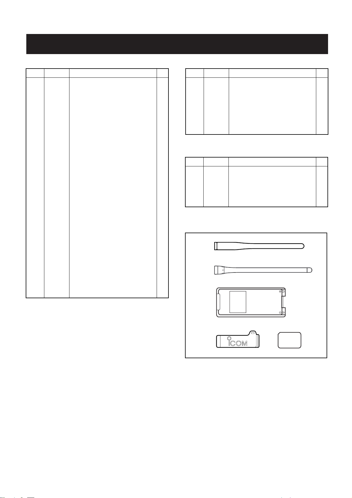
ORDERING PARTS
REPAIR NOTES
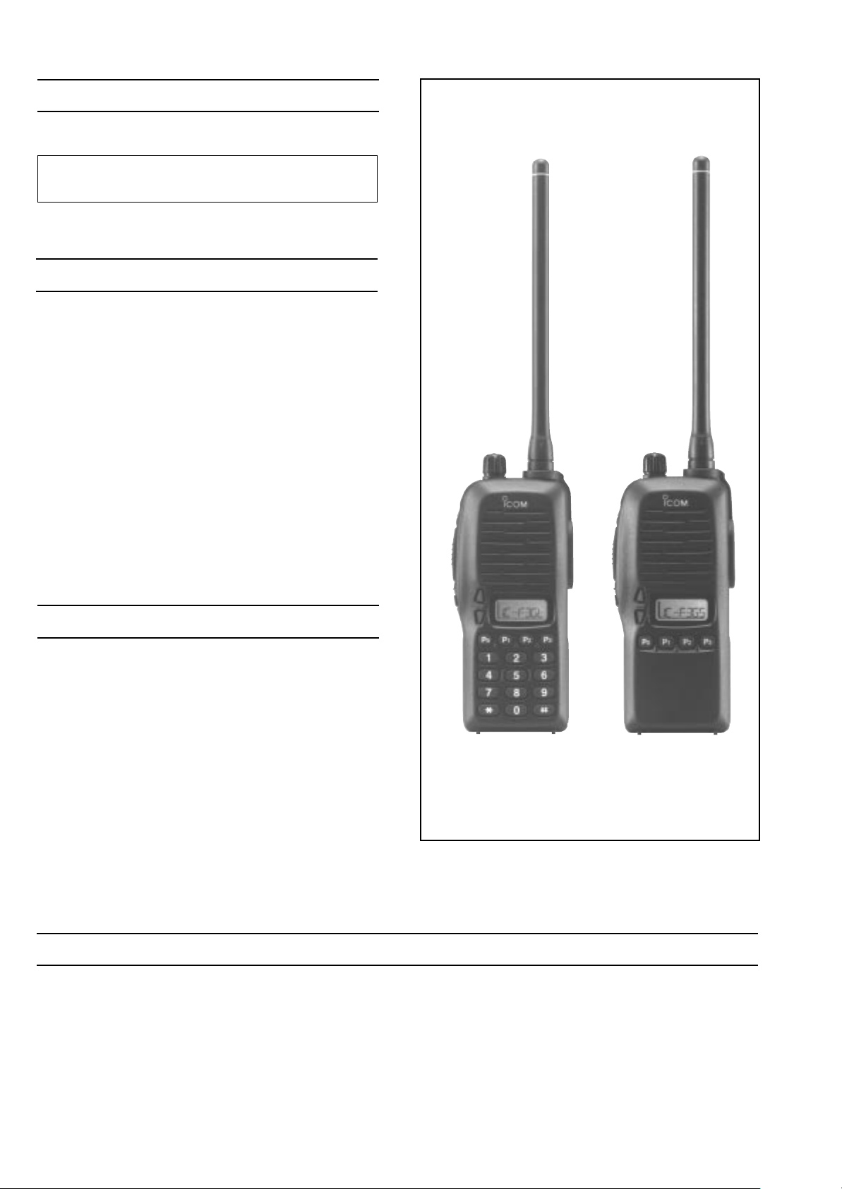
This service manual describes the latest service information
for the
IC-F3GT and IC-F3GS
at the time of publication.
NEVER connect the transceiver to an AC outlet or to a DC
power supply that uses more than 16 V. Such a connection
could cause a fire hazard and/or electric shock.
DO NOT expose the transceiver to rain, snow or any liquids.
DO NOT reverse the polarities of the power supply when con-
necting the transceiver.
DO NOT apply an RF signal of more than 20 dBm (100mW)
to the antenna connector. This could damage the transceiver’s front end.
Be sure to include the following four points when ordering
replacement parts:
1. 10-digit order numbers
2. Component part number and name
3. Equipment model name and unit name
4. Quantity required
<SAMPLE ORDER>
1130007610 S.IC µPD3140GS IC-F3GT MAIN UNIT 1 pieces
8810009510 Screw BT M2 x 4 NI-ZU IC-F3GS Chassis 10 pieces
Addresses are provided on the inside back cover for your
convenience.
1. Make sure a problem is internal before disassembling the transceiver.
2. DO NOT open the transceiver until the transceiver is disconnected from its power source.
3. DO NOT force any of the variable components. Turn them slowly and smoothly.
4. DO NOT short any circuits or electronic parts. An insulated turning tool MUST be used for all adjustments.
5. DO NOT keep power ON for a long time when the transceiver is defective.
6. DO NOT transmit power into a signal generator or a sweep generator.
7. ALWAYS connect a 40 dB to 50 dB attenuator between the transceiver and a deviation meter or spectrum analyzer when
using such test equipment.
8. READ the instructions of test equipment thoroughly before connecting equipment to the transceiver.
To upgrade quality, all electrical or mechanical parts and
internal circuits are subject to change without notice or obligation.
IC-F3GT
IC-F3GS
Page 3

TABLE OF CONTENTS
SECTION 1 SPECIFICATIONS
SECTION 2 INSIDE VIEWS
SECTION 3 DISASSEMBLY AND OPTION INSTRUCTIONS
3-1 DISASSEMBLY INSTRUCTION . . . . . . . . . . . . . . . . . . . . . . . . . . . . . . . . . . . . . . . . . . . . . .3-1
3-2 OPTIONAL UNIT INSTALLATIONS . . . . . . . . . . . . . . . . . . . . . . . . . . . . . . . . . . . . . . . . . . . .3-2
SECTION 4 CIRCUIT DESCRIPTION
4-1 RECEIVER CIRCUITS . . . . . . . . . . . . . . . . . . . . . . . . . . . . . . . . . . . . . . . . . . . . . . . . . . . . .4-1
4-2 TRANSMITTER CIRCUITS . . . . . . . . . . . . . . . . . . . . . . . . . . . . . . . . . . . . . . . . . . . . . . . . .4-1
4-3 PLL CIRCUITS . . . . . . . . . . . . . . . . . . . . . . . . . . . . . . . . . . . . . . . . . . . . . . . . . . . . . . . . . . .4-2
4-4 POWER SUPPLY CIRCUITS . . . . . . . . . . . . . . . . . . . . . . . . . . . . . . . . . . . . . . . . . . . . . . . .4-3
4-5 CPU PORT CIRCUITS . . . . . . . . . . . . . . . . . . . . . . . . . . . . . . . . . . . . . . . . . . . . . . . . . . . . .4-4
SECTION 5 ADJUSTMENT PROCEDURES
5-1 PREPARATION . . . . . . . . . . . . . . . . . . . . . . . . . . . . . . . . . . . . . . . . . . . . . . . . . . . . . . . . . .5-1
5-2 PLL ADJUSTMENT . . . . . . . . . . . . . . . . . . . . . . . . . . . . . . . . . . . . . . . . . . . . . . . . . . . . . . .5-3
5-3 TRIMMER ADJUSTMENT . . . . . . . . . . . . . . . . . . . . . . . . . . . . . . . . . . . . . . . . . . . . . . . . . .5-4
5-4 TRANSMITTER ADJUSTMENT . . . . . . . . . . . . . . . . . . . . . . . . . . . . . . . . . . . . . . . . . . . . . .5-6
5-5 RECEIVER ADJUSTMENT . . . . . . . . . . . . . . . . . . . . . . . . . . . . . . . . . . . . . . . . . . . . . . . . . .5-6
SECTION 6 PARTS LIST
SECTION 7 MECHANICAL PARTS AND DISASSEMBLY
SECTION 8 SEMI-CONDUCTOR INFORMATION
SECTION 9 BOARD LAYOUTS
9-1 GENERAL AND EIA/TIAVERSIONS (EXCEPT W/N-TYPE) . . . . . . . . . . . . . . . . . . . . . . . . .9-1
9-2 ETS/CEPT VERSION . . . . . . . . . . . . . . . . . . . . . . . . . . . . . . . . . . . . . . . . . . . . . . . . . . . . . .9-3
9-3 W/N-TYPE . . . . . . . . . . . . . . . . . . . . . . . . . . . . . . . . . . . . . . . . . . . . . . . . . . . . . . . . . . . . . .9-5
SECTION 10 BC-137 OPTIONAL DESKTOP CHARGER INFORMATION
10-1 PARTS LIST . . . . . . . . . . . . . . . . . . . . . . . . . . . . . . . . . . . . . . . . . . . . . . . . . . . . . . . . . . . . .10-1
10-2 DISASSEMBLY INFORMATION . . . . . . . . . . . . . . . . . . . . . . . . . . . . . . . . . . . . . . . . . . . . . .10-1
10-3 VOLTAGE DIAGRAM . . . . . . . . . . . . . . . . . . . . . . . . . . . . . . . . . . . . . . . . . . . . . . . . . . . . . .10-2
10-4 BOARD LAYOUT . . . . . . . . . . . . . . . . . . . . . . . . . . . . . . . . . . . . . . . . . . . . . . . . . . . . . . . . .10-2
SECTION 11 BLOCK DIAGRAM
SECTION 12 VOLTAGE DIAGRAM
Page 4
1 - 1
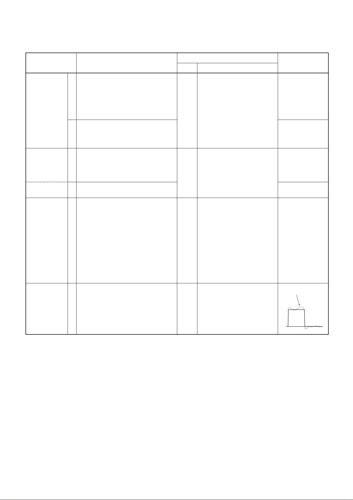
SECTION 1 SPECIFICATIONS
All stated specifications are subject to change without notice or obligation.
Frequency coverage
Type of emission
Number of channels
Power supply requirement
TX
at High
Current drain
at Low
(approx.)
RX
rated audio
stand-by
Frequency stability
Usable temperature range
Dimensions (proj. not included)
Weight (with BP-209)
Output power
Modulation system
Max. freqequency deviation
Spurious emissions
Adjacent channel power
Transmitter audio distortion
Limitting charact of modulator
Ext. microphone connector
Receive system
Intermediate frequencies
Sensitivity (typical)
Squelch sencitivity
Adjacent channel selectivity
Spurious response
Intermoduration rejection ratio
Hum and noise
Audio output power
(at 7.2 V DC)
External SP connector
ETS 300 086 EIA/TIA 603
RECEIVER TRANSMITTER GENERAL
136.000–150.000 MHz (L-band), 146.000–174.000 MHz (H-band)
16K0F3E (W-type), 14K0F3E (M-type), 8K50F3E (N-type)
100 ch (100 channel version),
32 ch (16 channels
× 2 banks: 2-BANK version), 16 ch (16 channel version)
7.2 V DC (negative ground; supplied battery pack)
1.6 A
700 mA
250 mA
70 mA
±2000 Hz (W/M-type), ±1.5 kHz (N-type) ±0.0005%
–25˚C to +55˚C –30˚C to +60˚C
54(W)
× 132(H) × 35(D) mm; 2
1
⁄8(W) × 57⁄32(H) × 13⁄8(D) inch
370 g; 13.1 oz
High 5 W
Low 1 W
Variable reactance frequency modulation
±5.0 kHz (W-type), ±4.0 kHz (M-type)*
1
, ±2.5 kHz (N-type)
0.25 µW @ < 1 GHz, 1.00 µW @ > 1 GHz 73 dBc typical
70 dB (W/M-type) 70 dB typical (W-type)
60 dB (N-type) 60 dB typical (N-type)
Less than 5% at 1 kHz, 60% deviation Less than 3% at 1 kHz, 40% deviation
70–100% of max. deviation
3-conductor 2.5(d) mm (1⁄10")/2.2 kΩ
Double-conversion superheterodyne system
1st: 31.05 MHz, 2nd: 450 kHz
0.25 µV at 12 dB SINAD
0.25 µV at 12 dB SINAD
0.63 µV (emf) at 20 dB SINAD
0.25 µV typical (at threshold)
70 dB (W/M-type) 75 dB typical (W-type)
60 dB (N-type) 65 dB typical (N-type)
70 dB 70 dB typical
65 dB 70 dB typical
45 dB typical (W/M-type) 45 dB typical (W-type)
43 dB typical (N-type) 40 dB typical (N-type)
500 mW typical at 5% distortion with an 8 Ω load
3-conductor 3.5(d) mm (
1
⁄8")/8 Ω
Measurements made in accordance with EIA/TIA-152-C, 204-D, 603 or ETS 300-086.
Page 5
2 - 1
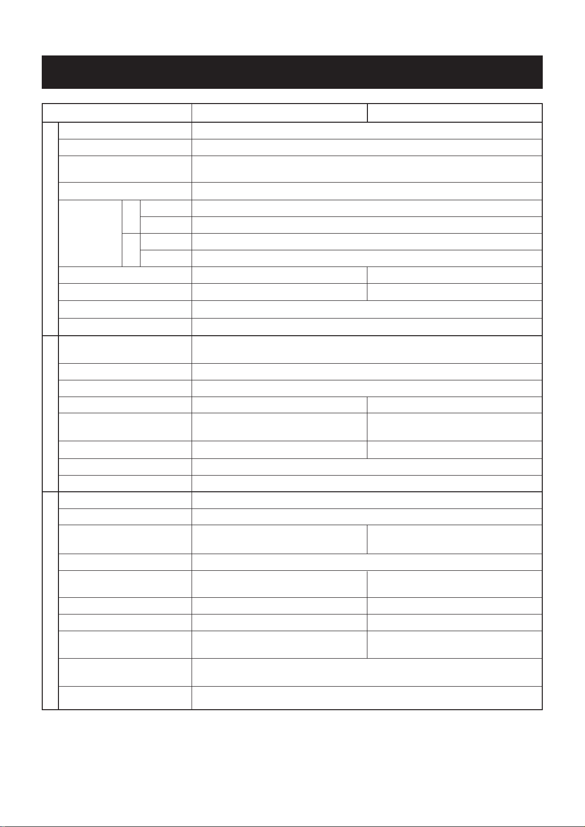
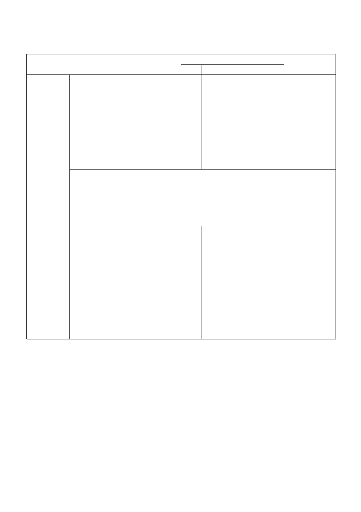
SECTION 2 INSIDE VIEWS
• MAIN UNIT
Power amplifier
(Q1: 2SK2974)
Antenna swtching circuit
(D1, D2, D8: MA77)
TOP VIEW BOTT OM VIEW
RF amplifier
(Q12: 3SK293)
VCO circuit
1st mixer
Q13: 3SK239A [OTHER]
3SK320 B
Low-pass filter circuit
TX/RX switch
(D3, D4: MA77)
Mic amplifier circuit
APC
IC3A: NJM2902V
Q37: DTA144EU
FM IF IC
(IC2: TA31136FN(D))
CPU
(IC8: HD6433876B50H)
EEPROM
IC7: HN58X2432TI [OTHER]
HN58X2464TI H
D/A converter
(IC10: M62363FP-650C)
PLL reference oscillator
X1: CR-664A 15.3 MHz [OTHER]
CR-671A 15.3 MHz A, D
Crystal filter
FI1: FL-311 [OTHER]
FL-312 C
FL-333 F, G
FL-334 E
PLL IC
(IC1: µPD3140GS)
IF amplifier
(Q14: 2SC4215 O)
()
()
()
()
()
A: W/N-type B: ETS/CEPT version
C: W-type of [GEN] D: EIA/TIA version
E: W-type of ETS/CEPT version F: N-type of ETS/CEPT version
G: M (20 kHz)-type H: 100 channel version
Page 6
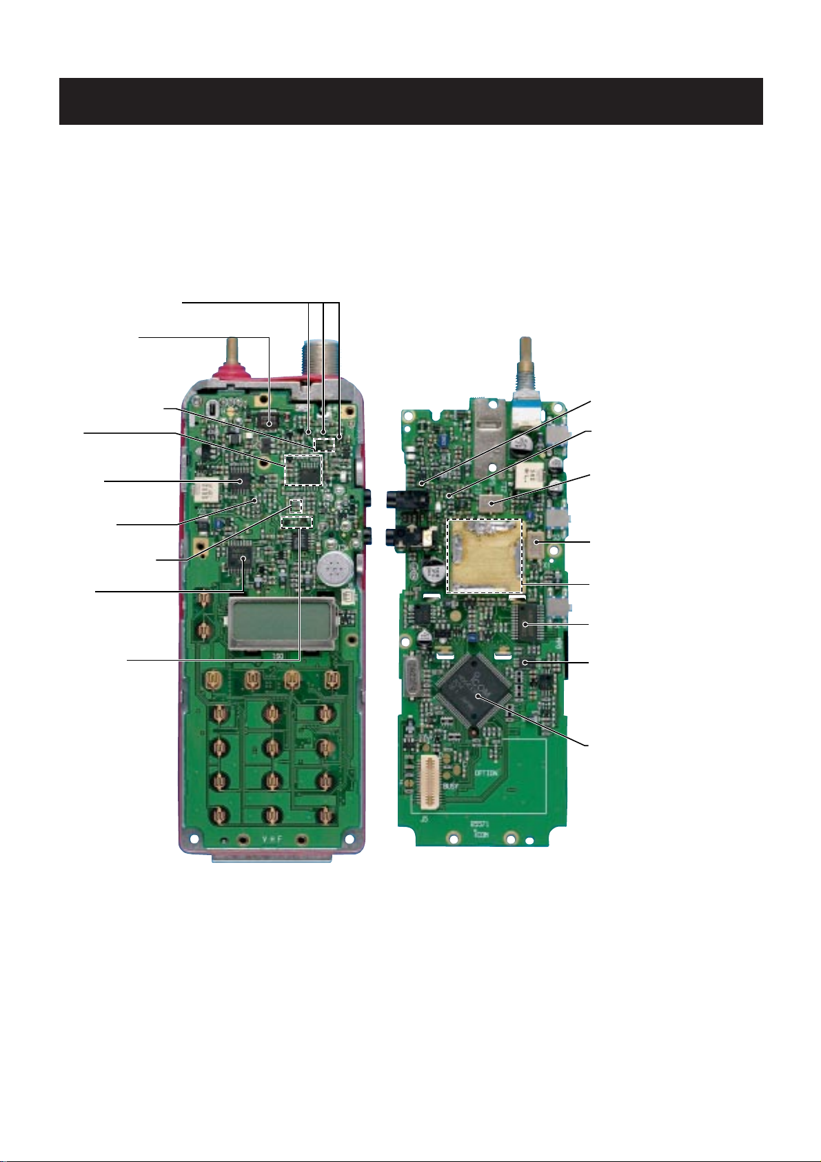
3 - 1
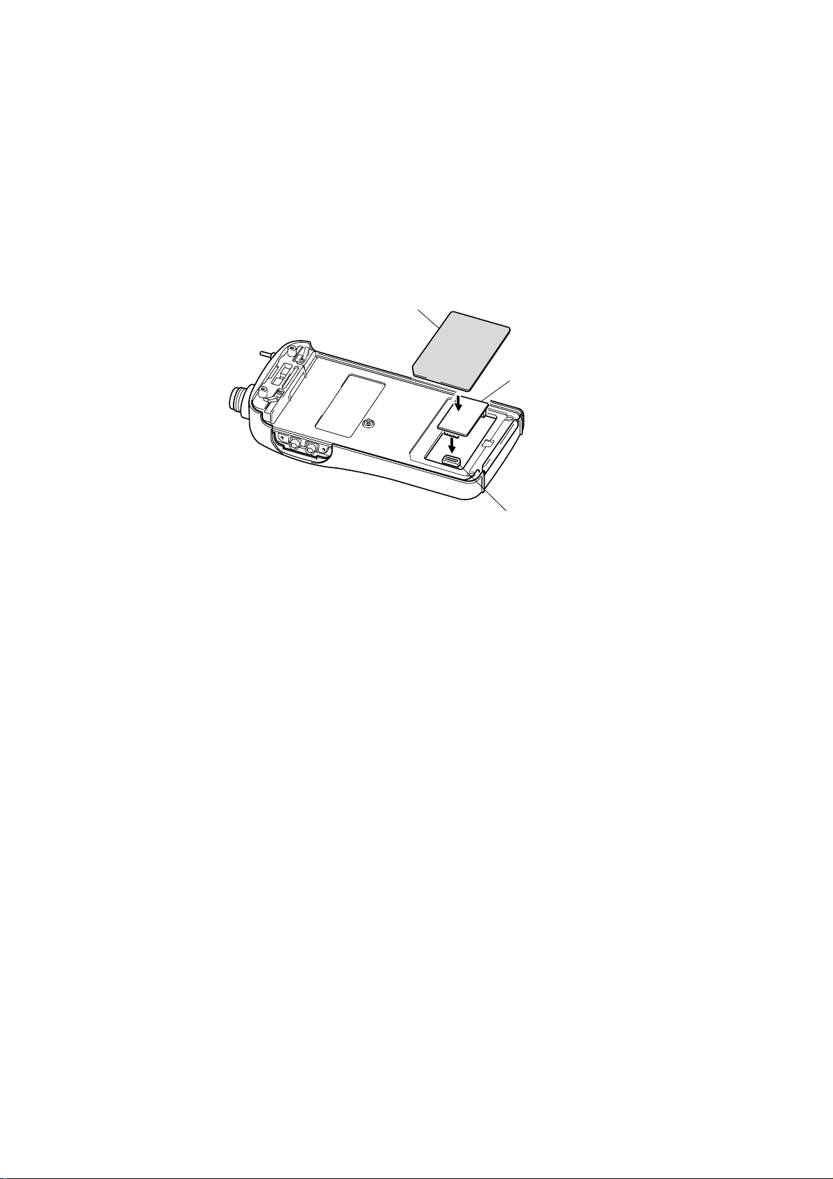
SECTION 3 DISASSEMBLY AND OPTION INSTRUCTIONS
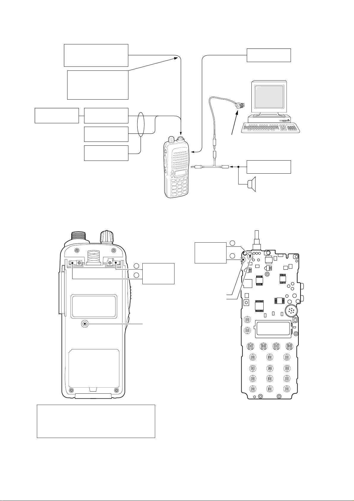
3-1 DISASSEMBLY INSTRUCTION
• REMOVING THE CHASSIS PANEL
1 Unscrew 1 nut A, and remove 1 knob B.
2 Unscrew 2 screws C.
3 Take off the chassis in the direction of the arrow.
4 Unplug J6 to separate front panel and chassis.
• REMOVING THE MAIN UNIT
1 Remove the searing rubber.
2 Unsolder 4 points D, and unscrew 1 nut E.
3 Unscrew 3 screws F and 6 screws G (silver, 2 mm) to separate the chassis and the MAIN unit.
4 Take off the MAIN unit in the direction of the arrow.
(nickel, 2 mm) x 2
Front panel
Chassis
J6 (Speaker connector)
B
C
A
F
(black, 2 mm) x 2
(silver, 2 mm) x 6
Shield cover
Guide holes
MAIN unit
Sealing rubber
Chassis
F
D
D
G
D
E
G
G
Page 7
3 - 2
3-2 OPTIONAL UNIT INSTALLATIONS
1 Remove the option cover.
2 Connect one of UT-96, UT-105, UT-108, UT-109, UT-110, and UT-111 optional unit to J5.
3 Replace the option cover to the chassis-hole.
Option cover
Option unit
J5
Page 8
4 - 2
SECTION 4 CIRCUIT DESCRIPTION
4-1 RECEIVER CIRCUITS
4-1-1 ANTENNA SWITCHING CIRCUIT
Received signals are passed through the low-pass filter (L1,
L2, C1–C5, C8). The filtered signals are applied to the λ⁄4
type antenna switching circuit (D2, D8).
The antenna switching circuit functions as a low-pass filter
while receiving. However, its impedance becomes very high
while D2 and D8 are turned ON. Thus transmit signals are
blocked from entering the receiver circuits. The antenna
switching circuit employs a λ⁄4 type diode switching system.
The passed signals are then applied to the RF amplifier circuit.
4-1-2 RF CIRCUIT
The RF circuit amplifies signals within the range of frequency coverage and filters out-of-band signals.
The signals from the antenna switching circuit are amplified
at the RF amplifier (Q12) after passing through the tunable
bandpass filter (D9, D10, L16, L17, C78–C80, C83, C86,
C277). The amplified signals are applied to the 1st mixer circuit (Q13) after out-of-band signals are suppressed at the
tunable bandpass filter (D11, D12, L18, L19, C91, C92, C94,
C96–C98).
Varactor diodes are employed at the bandpass filters that
track the filters and are controlled by the CPU (IC8) via the
expander IC (IC10) using T1–T4 signals. These diodes tune
the center frequency of an RF passband for wide bandwidth
receiving and good image response rejection.
4-1-3 1ST MIXER AND 1ST IF CIRCUITS
The 1st mixer circuit converts the received signal into a fixed
frequency of the 1st IF signal with a PLL output frequency.
By changing the PLL frequency, only the desired frequency
will pass through a crystal filter at the next stage of the 1st
mixer.
The signals from the RF circuit are mixed at the 1st mixer
(Q13) with a 1st LO signal coming from the VCO circuit to
produce a 31.05 MHz 1st IF signal.
The 1st IF signal is applied to two crystal filters (FI1) to suppress out-of-band signals. The filtered 1st IF signal is
applied to the IF amplifier (Q14), then applied to the 2nd
mixer circuit (IC2, pin 16).
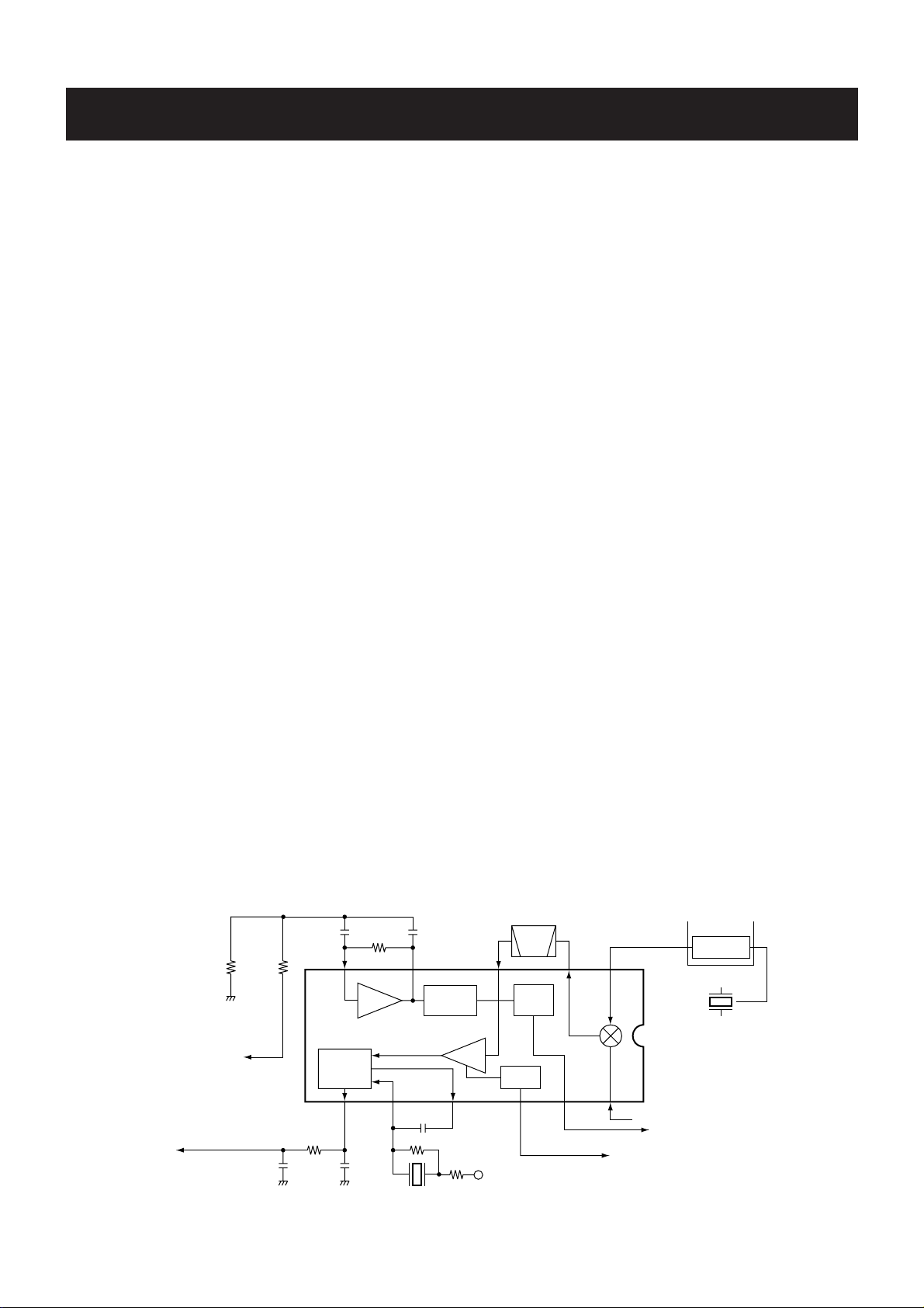
4-1-4 2ND IF AND DEMODULATOR CIRCUITS
The 2nd mixer circuit converts the 1st IF signal into a 2nd IF
signal. Adouble conversion superheterodyne system (which
converts receive signals twice) improves the image rejection
ratio and obtains stable receiver gain.
The 1st IF signal from the IF amplifier is applied to the 2nd
mixer section of the FM IF IC (IC2, pin 16), and is mixed with
the 2nd LO signal to be converted into a 450 kHz 2nd IF signal.
The FM IF IC contains the 2nd mixer, limiter amplifier, quadrature detector and active filter circuits. A 2nd LO signal
(30.6 MHz) is produced at the PLL circuit by doubling it’s reference frequency.
The 2nd IF signal from the 2nd mixer (IC2, pin 3) passes
through a ceramic filter (FI2) to remove unwanted heterodyned frequencies. It is then amplified at the limiter amplifier (IC2, pin 5) and applied to the quadrature detector (IC2,
pins 10, 11) to demodulate the 2nd IF signal into AF signals.
• 2nd IF and demodulator circuits
Mixer
16
Limiter
amp.
2nd IF filter
450 kHz
PLL IC
IC1
X1
15.3 MHz
IC2 TA31136F
12
1st IF from the IF amplifier (Q14)
"SD" signal to the CPU pin 98
11109
87 5 3
AF signal "DET"
R5
X3
R86
C122
C121
R88R87
R83
"SQLIN" signal from the
D/A convertor (IC10, pin 23)
R82
C112 C113
C116
2
17 16
Active
filter
FI2
Noise
detector
FM
detector
13
"NOIS" signal to the CPU pin 19
RSSI
Noise
comp.
×2
R84
Page 9
4 - 3
4-1-5 AF CIRCUIT
AF signals from the FM IF IC (IC2, pin 9) are applied to the
mute switch (IC4, pin 1) via the AF filter circuit (IC3b, pins 6,
7). The output signals from pin 11 are applied to the AF
power amplifier (IC5, pin 4) after being passed through the
[VOL] control (R143).
The applied AF signals are amplified at the AF power amplifier circuit (IC5, pin 4) to obtain the specified audio level. The
amplified AF signals, output from pin 10, are applied to the
internal speaker (SP1) as the “SP” signal via the [SP] jack
when no plug is connected to the jack.
4-1-6 SQUELCH CIRCUIT
Asquelch circuit cuts out AF signals when no RF signals are
received. By detecting noise components in the AF signals,
the squelch switches the AF mute switch.
Aportion of the AF signals from the FM IF IC (IC2, pin 9) are
applied to the active filter section (IC2, pin 8) where noise
components are amplified and detected with an internal
noise detector.
The active filter section amplifies noise components. The filtered signals are rectified at the noise detector section and
converted into “NOIS” (pulse type) signals at the noise comparator section. The “NOIS” signal is applied to the CPU
(IC8, pin 19).
The CPU detects the receiving signal strength from the
number of the pulses, and outputs an “RMUT” signal from
pin 49. This signal controls the mute switch (IC4) to cut the
AF signal line.
4-1-7 WIDE AND NARROW SWITCHING CIRCUIT
The “NWC” signal from the CPU (IC8, pin 38) is applied to
the Q41. Q41 is switched ON or OFF by the signal. Q41 controls IC2’s detector output to same level both wide band
mode and narrow band mode.
4-2 TRANSMITTER CIRCUITS
4-2-1 MICROPHONE AMPLIFIER CIRCUIT
The microphone amplifier circuit amplifies audio signals with
+6 dB/octave pre-emphasis characteristics from the microphone to a level needed for the modulation circuit.
The AF signals from the microphone are applied to the
microphone amplifier circuit (IC3c, pin 10). The amplified AF
signals are passed through the low-pass filter circuit (IC3d,
pins 13, 14) via the mute switch (IC4, pins 4, 3, 2). The filtered AF signals are applied to the modulator circuit after
being passed through the mute switch (IC4, pins 9, 8).
4-2-2 MODULATION CIRCUIT
The modulation circuit modulates the VCO oscillating signal
(RF signal) using the microphone audio signal.
The audio signals from the D/A convertor (IC10, pin 22)
change the reactance of a diode (D6) to modulate an oscillated signal at the VCO circuit (Q7, Q8). The oscillated signal is amplified at the buffer-amplifiers (Q4, Q6), then
applied to the T/R switching circuit (D3, D4).
4-2-3 DRIVE/POWER AMPLIFIER CIRCUITS
The signal from the VCO circuit passes through the T/R
switching circuit (D3) and is amplified at the buffer (Q3),
drive (Q2) and power amplifier (Q1) to obtain 5 W of RF
power (at 7.2 V DC). The amplified signal passes through
the antenna switching circuit (D1), and low-pass filter and is
then applied to the antenna connector.
The bias current of the drive (Q2) and the power amplifier
(Q1) is controlled by the APC circuit.
4-2-5 APC CIRCUIT
The APC circuit (IC3a, Q37) protects the drive and the
power amplifiers from excessive current drive, and selects
HIGH or LOW output power.
• APC circuit
Q1
Power
amp.
Q2
Driver
amp.
IC3a
+
–
VCC
RF signal
from PLL
to antenna
T4
TXC
Q37
S5
APC control circuit
Power detector
circuit (D32, D33)
D33 D32
L4, C278, C287
LPF
Page 10
4 - 4
The signal output from the power detector circuit (D32, D33)
is applied to the differential amplifier (IC3a, pin 2), and the
“T4” signal from the expander (IC10, pin 11), controlled by
the CPU (IC8), is applied to the other input for reference.
When the driving current is increased, input voltage of the
differential amplifier (pin 2) will be increased. In such cases,
the differential amplifier output voltage (pin 1) is decreased
to reduce the driving current.
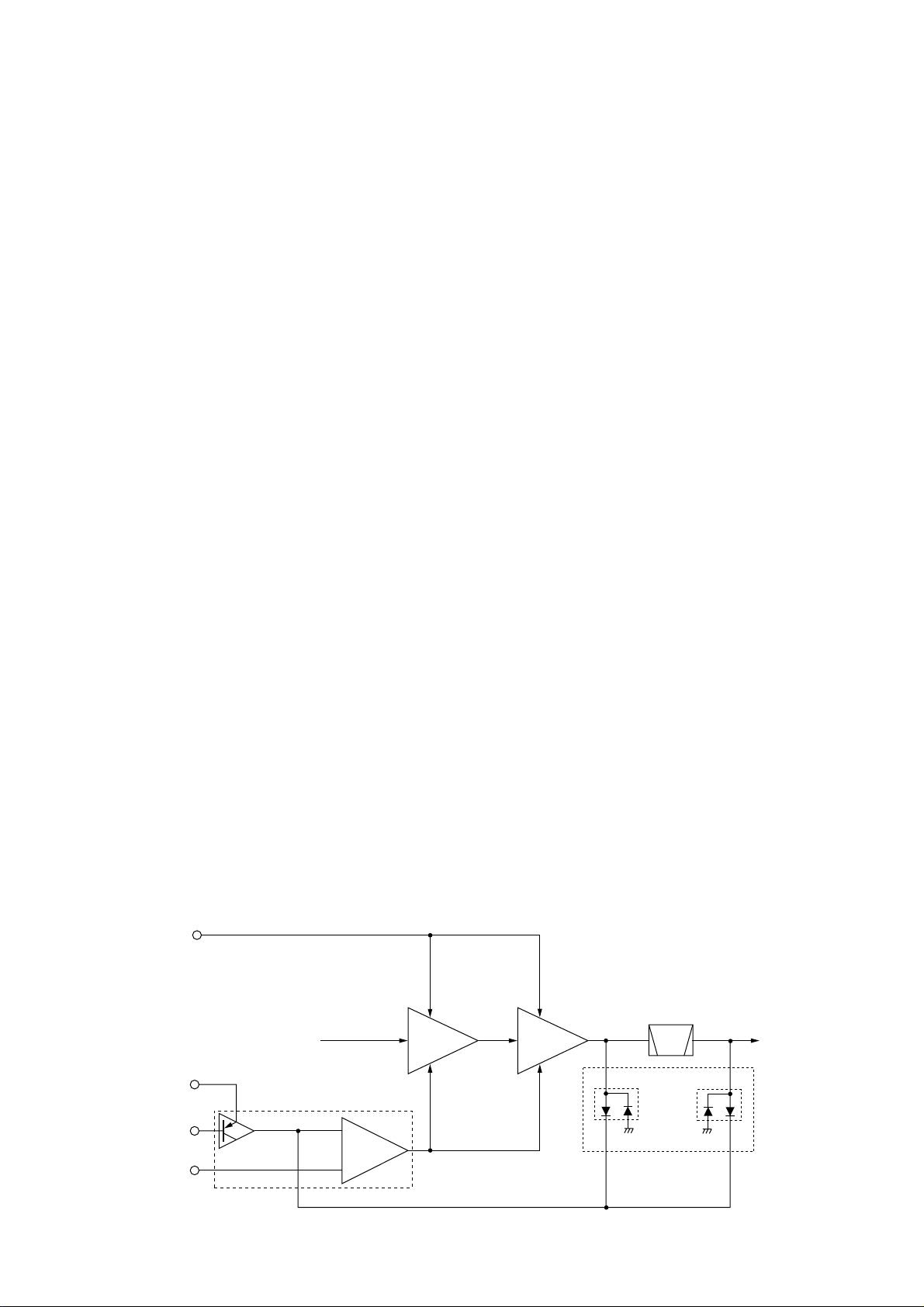
4-3 PLL CIRCUIT
A PLL circuit provides stable oscillation of the transmit frequency and receive 1st LO frequency. The PLL output compares the phase of the divided VCO frequency to the reference frequency. The PLL output frequency is controlled by
the divided ratio (N-data) of a programmable divider.
The PLL circuit contains the VCO circuit (Q7, Q8). The oscillated signal is amplified at the buffer-amplifiers (Q6, Q5) and
then applied to the PLL IC (IC1, pin 2).
The PLL IC contains a prescaler, programmable counter,
programmable divider and phase detector, etc. The entered
signal is divided at the prescaler and programmable counter
section by the N-data ratio from the CPU. The divided signal
is detected on phase at the phase detector using the reference frequency.
If the oscillated signal drifts, its phase changes from that of
the reference frequency, causing a lock voltage change to
compensate for the drift in the oscillated frequency.
A portion of the VCO signal is amplified at the buffer-amplifier (Q4) and is then applied to the receive 1st mixer (Q13)
or transmit buffer-amplifier circuit (Q3) via the T/R switching
diode (D3, D4).
4-4 POWER SUPPLY CIRCUITS
VOLTAGE LINE
• PLL circuit
Shift register
×2
Prescaler
Phase
detector
Loop
filter
Programmable
counter
Programmable
divider
X1
15.3 MHz
30.6 MHz signal
to the FM IF IC
"DEV" signal from the
D/A convertor (IC10, pin 22)
when transmitting
16
Q7, Q8
VCO circuit
Buffer
Q6
Buffer
Q4
Buffer
Q5
3
4
5
PLST
SCK
SO
to transmitter circuit
to 1st mixer circuit
D4
D3
17
8
2
LINE
HV
VCC
5V
T5
R5
S5
OPT
CPU5
DESCRIPTION
The voltage from the attached battery pack.
The same voltage as the HV line (battery volt-
age) which is controlled by the power swtich
([VOL] control).
Common 5 V converted from the VCC line by the
reference regulator circuit (IC6). The output voltage is applied to the 5 V regulator circuit (Q18,
Q19).
5 V for transmitter circuits regulated by the T5
regulator circuit (Q22).
5 V for receiver circuits regulated by the R5 regulator circuit (Q21).
Common 5 V converted from the VCC line by the
S5 regulator circuit (Q18, Q19).
The same voltage as the 5V line for the optional
HM-46L, EM-71 or HS-51 through a resistor
(R132).
The same voltage as the 5V line which is regulated by +5 V CPU regulator circuit (IC6). The
voltage is applied to the reset circuit (IC11) and
CPU (IC8).
Page 11
4 - 5
4-5 PORT ALLOCATIONS
4-5-1 CPU (IC8)
Pin
number
1
9
11
12
15
16
17
18
19
21
26, 36,
37
38
44–47
49
50
51
52
53
54
55
56
57
58
59
Port
name
VIN
RESET
CSIFT
SCK
DAST
CLIN
CLOUT
PLST
NOIS
BUSY
OPV1–3
NWC
KR3–
KR0
RMUT
MMUT
DUSE
S5C
R5C
T5C
TXC
AFON
LIGT
ESCK
ESDA
Description
Input port for battely voltage detection.
Input port for RESET signal.
Outputs reference oscillator for the
CPU control signal.
Outputs clock signal to the PLL IC
(IC1), EEPROM (IC7), etc.
• Outputs strobe signals to the
expander IC (IC10, pin 6).
• Input port for the initial version signal.
Input port for the cloning signal.
Outputs the cloning signal.
Outputs strobe signals to the PLL IC
(IC1, pin 3).
Input for for noise signals (pulse type).
Outputs BUSY detection.
Low: The channel is busy.
Input port for the optional unit detection signal from J5.
Outputs Wide/Narrow mode control
signal.
High: Wide mode is selected.
Output ports for key matrix.
Low: When the key is pushed.
• Outputs RX mute control signal.
• Input port for the RX mute signal
from optional units.
• Output TX mute control signal.
• Input port for the TX mute signal
from optional units.
Outputs low-pass filter cut-off frequency control signal when DTCS is activated.
Outputs S5 regulator control signal.
Low: While power is ON.
Outputs R5 regulator control signal.
Low: While receiving.
Outputs T5 regulator control signal.
Low: While transmitting.
Outputs APC circuit control signal.
High: While transmitting.
Outputs control signal for the regulator
circuit of AF power amplifier.
High: When squelch is open, etc.
Outputs LCD backlight control signal.
High: Lights ON.
Outputs EEPROM (IC7, pin 6) clock
signal.
I/O port for data signals from/to EEPROM (IC7, pin 5)
Pin
number
63
90
91
94
95
96
97
98
99
100
Port
name
UNLK
MTONE
DTMF
CTCIN
PTT0
BDET
REM0
SD
LVIN
TEMP
Description
Input port for unlock signal.
High:PLL is unlocked.
Low: PLL is locked.
Output port for:
Beep audio while receiving.
2/5-tone signals while transmitting.
Outputs DTMF tone signal while transmitting.
CTCSS/DTCS signals input port for
decording.
Input port for the [PTT] switch.
High:While [PTT] switch is pushed.
Input port for the battery’s type detection.
Input port for the remote-control signal
from external MIC (HM-75).
Input port for the RSSI detection.
Input port for the PLL lock voltage.
Input port for the transceiver’s internal
temperature detection.
4-5-2 OUTPUT EXPANDER IC (IC10)
Pin
number
2, 3,
10, 11
6
7
Port
name
T1–T4
DAST
SCK
Description
Output tunable bandpass filter control
signals.
Input port for strobe signal from the
CPU (IC8, pin 15).
Input port for clock signal from the
CPU (IC8, pin 12).
CPU (IC8)–continued
Page 12

5 - 1
SECTION 5 ADJUSTMENT PROCEDURES
5-1 PREPARATION
When you adjust the contents on page 5-5 or 5-6, SOFTWARE ADJUSTMENT, the optional CS-F3G ADJ ADJUSTMENTSOFTWARE
(Rev. 1.0 or later), OPC-478 CLONING CABLE and a JIG CABLE (see illustration at page 5-2) are required.
■ REQUIRED TEST EQUIPMENT
EQUIPMENT
DC power supply
RF power meter
(terminated type)
Frequency counter
FM deviation meter
Digital multimeter
GRADE AND RANGE
Output voltage : 7.2 V DC
Current capacity : 5 Aor more
Measuring range : 1–10 W
Frequency range : 120–500 MHz
Impedance : 50 Ω
SWR : Less than 1.2 : 1
Frequency range : 0.1–500 MHz
Frequency accuracy : ±1 ppm or better
Sensitivity : 100 mV or better
Frequency range : DC–500 MHz
Measuring range : 0 to ±5 kHz
Input impedance : 10 MΩ/V DC or better
EQUIPMENT
Audio generator
Attenuator
Standard signal
generator (SSG)
DC voltmeter
Oscilloscope
AC millivoltmeter
GRADE AND RANGE
Frequency range : 300–3000 Hz
Output level : 1–500 mV
Power attenuation : 40 or 50 dB
Capacity : 10 W or more
Frequency range : 120–500 MHz
Output level : 0.1 µV–32 mV
(–127 to –17 dBm)
Input impedance : 50 kΩ/V DC or better
Frequency range : DC–20 MHz
Measuring range : 0.01–20 V
Measuring range : 10 mV–10 V
■ SYSTEM REQUIREMENTS
• IBM PC compatible computer with an RS -232C serial port
(38400 bps or faster).
• Microsoft Windows 95 or Windows 98
• Intel i486DX processor or faster (Pentium 100 MHz or
faster recommended)
• At least 16 MB RAM and 10 MB of hard disk space
• 640×480 pixel display (800×600 pixel display recommended)
■ ADJUSTMENT SOFTWARE INSTALLATION
NOTE: Before using the program, make a backup copy of
the original disk. After making a backup copy, keep the original disk in a safe place.
q Boot up Windows.
- Quit all applications when Windows is running.
w Insert the backup disk1 into the appropriate floppy drive.
e Select ‘Run’ from the [Start] menu.
r Type the setup program name using the full path name,
then push the [Enter] key. (A:\ setup)
t Follow the prompts.
y Program group ‘CS-F3G ADJ’ appears in the ‘Programs’
folder of the [Start] menu.
■ STARTING SOFTWARE ADJUSTMENT
q Connect IC-F3GT/GS and PC with the optional OPC-478
and the JIG cable.
w Boot up Windows, and turn the transceiver power ON.
e Click the program group ‘CS-F3G ADJ’ in the ‘Programs’
folder of the [Start] menu, then CS-F3G ADJ’s window is
appeared.
r Click ‘Connect’ on the CS-F3G’s window, then appears
IC-F3GT/GS’s up-to-date condition.
t Set or modify adjustment data as desired.
IBM is a registered trademark of International Bussiness
Machines Corporation in the U.S.A. and other countries.
Microsoft and Windows are registered trademarks of
Microsoft Corporation in the U.S.A. and other countries.
Screen shots produced with permission from Microsoft
Corporation. All other products or brands are registered
trademarks or trademarks of their respective holders.
Page 13
5 - 2
¥ JIG cable
+
( CLONE)
—
( GND)
+
( SP)
—
( SPE)
3-conductor 3.5(d) mm plug
OPC-478
JIG cable
to IC-F3GT/GS [SP] jack
CS-F3G ADJ Rev.2.0
File
COM 1: OPEN
Option
Connect
Reload (F5) Disp para
[A / D]
VIN : 197 : C5h : 7.73 V
TEMPS : 190 : BEh : 32.23 'C
L VIN : 98 : 62h : 1.92 V
SD : 0 : 00h : 0.00 V
REMOT : 14 : 0Eh : 0.27 V
BDET : 255 : FFh : 5.00 V
Power (Hi) : 98 [ # # # # # # # # – – – – – – – – – – – ]
Power (Lo) : 54 [ # # # # – – – – – – – – – – – – – – – ]
DTCS BAL : 132 [ # # # # # # # # # # – – – – – – – – – ]
MOD : 95 [ # # # # # # # – – – – – – – – – – – – ]
SQL : 85 [ # # # # # # # – – – – – – – – – – – – ]
BPF ALL : [Enter] to sweep
BPF T1 : 23 [ # # # # # # # # # # # # – – – – – – – ] [Enter] to sweep
BPF T2 : –22 [ # # # # # # # # – – – – – – – – – – – ] [Enter] to sweep
BPF T3 : 9 [ # # # # # # # # # # # – – – – – – – – ] [Enter] to sweep
BPF T4 : –7 [ # # # # # # # # # – – – – – – – – – – ] [Enter] to sweep
TXF : [Enter] to start
[D / A]
BPF T1 : 90 : 5Ah : 1.76 V
BPF T2 : 45 : 2Dh : 0.88 V
BPF T3 : 76 : 4Ch : 1.49 V
T4/POW : 60 : 3Ch : 1.18 V
REF : 112 : 70h : 2.20V
DTCS BL.: 90 : 5Ah : 1.76 V
Dev : 45 : 2Dh : 0.88 V
SQL Lev : 0 : 00h : 1.18 V
CH No. : 01 (RX Freq = 216.050, TX Freq = <– ) RF Power: High
TCXO
: Transceiver's connection state
: Reload adjustment data
: Receive sensitivity measurement
: Connected DC voltage
: PLL lock voltage
: Operating channel select
: RF output power
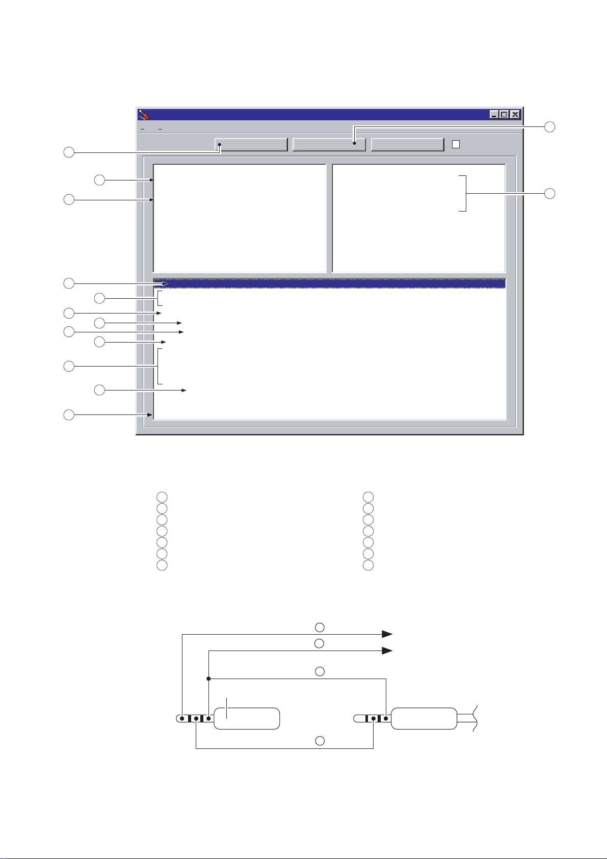
NOTE:
• Screen display exampe
1
5
4
6
10
11
12
14
1
2
3
4
5
6
7
8
9
10
11
12
13
14
: DTCS wave balance
: FM deviation
: Squelch level
: Receive sensitivity (automatically)
: Receive sensitivity (manually)
: Reference frequency
: Adjustment items
The above values for settings are example only.
Each transceiver has its own specific values for each setting.
3
2
8
9
7
13
Page 14
5 - 3
to an RS-232C port
Personal
computer
to [MIC]
to [SP]
JIG cable
DB9 female plug
(incl. level converter circuit)
• Connection
to the antenna connector
RF power meter
0.1–10 W/50 Ω
Frequency
counter
Attenuator
40 dB or 50 dB
FM
deviation meter
Standard signal generator
0.1 µV to 32 mV
(–127 dBm to –17 dBm)
SINAD meter
Speaker (8 Ω)
Audio generator
OPC-478
CAUTION:
DO NOT transmit while
an SSG is connected to
the antenna connector.
DC POWER
SUPPLY
GND
¥ DC power cable connections
SOFTWARE ADJUSTMENT
PLL ADJUSTMENT
—
Top view
Soldering
DC cable here
+
—
+
DC POWER
SUPPLY
Battery type detectorBattery type detector
NOTE: When you adjust the output power (high
power), the battery type detector must be connected to GND (see illustration at above).
Ohterwise the transceiver does not transmit high
power, the output power will be low.
Page 15
5 - 4
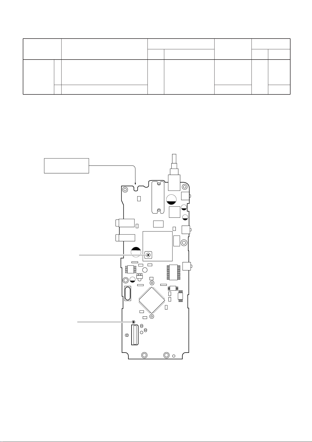
5-2 PLL ADJUSTMENT
PLL LOCK
VOLTAGE
1
2
• Operating frequency :
136.000 MHz (L-band)
146.000 MHz (H-band)
• Receiving
• Transmitting
MAIN Connect a digital multi
meter to check point
LV.
2.0 V
1.5–2.5 V
MAIN L11
Verify
ADJUSTMENT ADJUSTMENT CONDITIONS
UNIT LOCATION
VALUE
UNIT ADJUST
MEASUREMENT ADJUSTMENT
L11
PLL lock voltage
adjustment
LV
PLL lock voltage
check point
• MAIN unit
Bottom view
RF power meter
Page 16
5 - 6
1
2
1
2
1
1
• Operating frequency:
136.000 MHz (L-band)
146.000 MHz (H-band)
• High/Low switch : Low
• Connect the RF power meter or 50 Ω
dummy load to the antenna connector.
• Transmitting
• Transmitting
• Operating frequency:
136.000 MHz (L-band)
146.000 MHz (H-band)
• High/Low switch : Low
• Transmitting
• High/Low switch : High
• Transmitting
• Operating frequency:
136.000 MHz (L-band)
146.000 MHz (H-band)
• High/Low switch : Low
• Connect the audio generator to the
[MIC] jack and set as
:
1.0 kHz/150 mVrms
• Set the FM deviation meter as:
HPF : OFF
LPF : 20 kHz
De-emphasis : OFF
Detector : (P–P)/2
• Transmitting
• Operating frequency:
143.000 MHz (L-band)
160.000 MHz (H-band)
• High/Low switch : Low
• No audio applied to the [MIC] jack.
• DTCS code : 007
• Transmitting
REFERENCE
FREQUENCY
[TXF]
OUTPUT
POWER
[POWER (LO)]
[POWER (HI)]
FM
DEVIATION
[MOD]
DTCS WAVE
FORM
[DTCS BAL]
Top
panel
Top
panel
Top
panel
Top
panel
Loosely couple a frequnecy
counter to the antenna connector.
Connect an RF power meter to
the antenna connector.
Connect an FM deviation meter
to the antenna connector
through the attenuator.
Connect an FM deviation meter
with an oscilloscope to the
antenna connector through an
attenuator.
136.00000 MHz
(L-band)
146.00000 MHz
(H-band)
136.001360 MHz
(L-band)
146.001460 MHz
(H-band)
1.0 W
5.0 W
±4.1 kHz (W-type)*
1
±3.3 kHz (M-type)
±2.0 kHz (N-type)*
1
ADJUSTMENT ADJUSTMENT CONDITION
MEASUREMENT
VALUE
UNIT
LOCATION
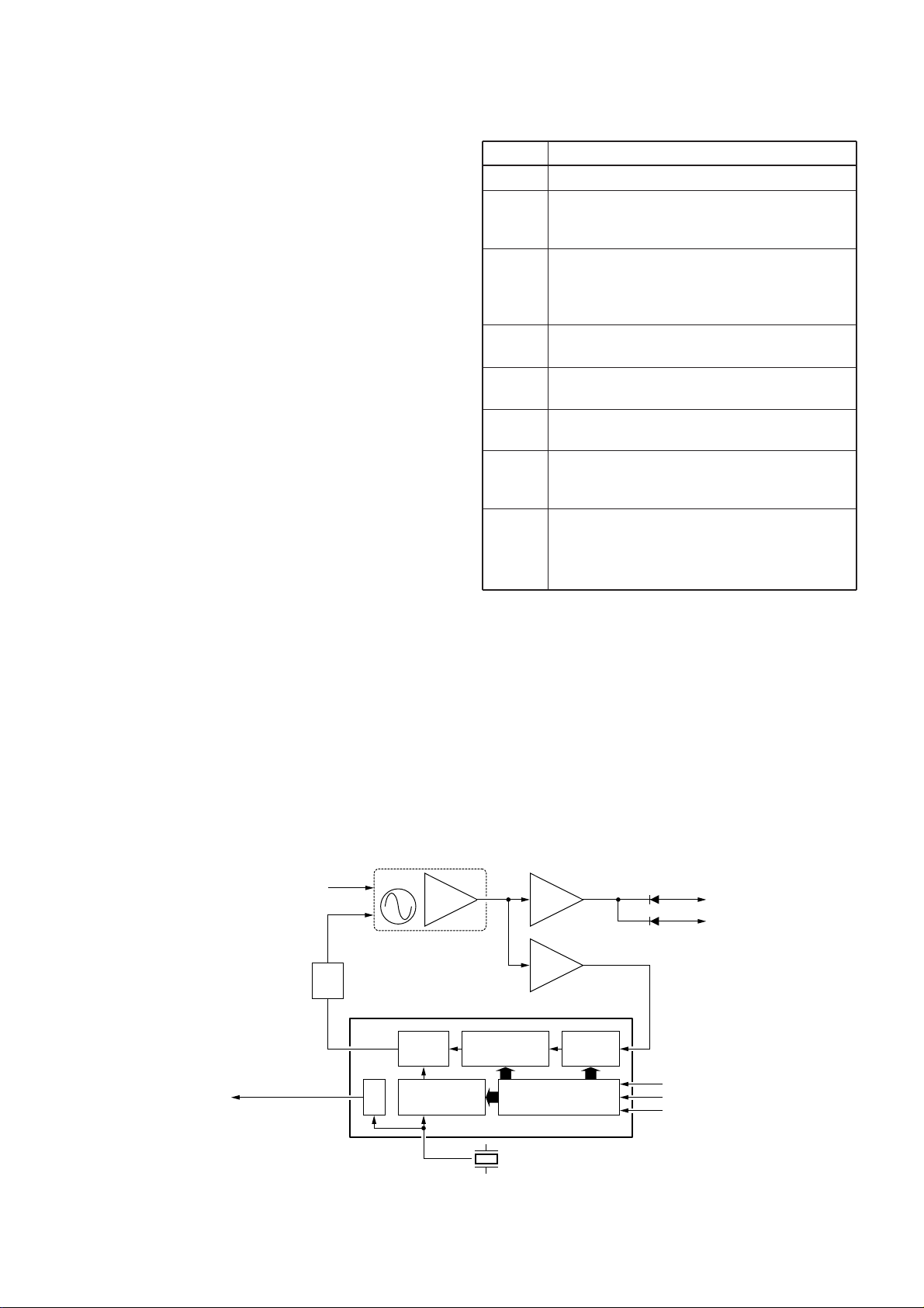
5-3 SOFTWARE ADJUSTMENT
Select an operation using [↑] / [↓] keys, then set specified value using [←] / [→] keys on the connected computer keyboard.
Set to flat wave
form
*1W/N-type must adjust both (W-type) and (N-type).
Page 17
5 - 7
Minimum distortion
level
12 dB SINAD
At the point where
the audio signals
just appears.
1
• Operating frequency:
136.000 MHz (L-band)
146.000 MHz (H-band)
• Connect a standard signal generator to
the antenna connector and set as:
Frequency : 136.000 MHz (L-band)
: 146.000 MHz (H-band)
Level :
5.6 µV* (–92 dBm
)
Modulation : 1 kHz
Deviation : ±3.5 kHz (W-type)*
1
±2.8 kHz (M-type)
±1.75 kHz (N-type)
*
1
• Set the NARROW ch. [W/N-type] only
• Receiving
• Operating frequency:
136.000 MHz (L-band)
146.000 MHz (H-band)
• Connect a standard signal generator to
the antenna connector and set as:
Frequency : 136.000 MHz (L-band)
146.000 MHz (H-band)
Level : OFF
Modulation : 1 kHz
Deviation : ±3.5 kHz (W-type)*
1
±2.8 kHz (M-type)
±1.75 kHz (N-type)
*
1
• Receiving
• Receiving
RX
SENSITIVITY
[BPF T1] –
[BPF T4]
SQUELCH
LEVEL
[SQL]
Top
panel
Top
panel
Connect a SINAD meter with an
8Ω load to the [SP] jack.
Connect a SINAD meter with an
8Ω load to the [SP] jack.
ADJUSTMENT ADJUSTMENT CONDITION
MEASUREMENT
VALUE
UNIT
LOCATION
*The output level of the standard signal generator (SSG) is indicated as the SSG’s open circuit.
SOFTWARE ADJUSTMENT – continued
Select an operation using [↑] / [↓] keys, then set specified value using [←] / [→] keys on the connected computer keyboard.
CONVENIENT: The BPF T1–BPF T4 can be adjusted automatically.
q-1: Set the cursol to “BPF ALL” on the adjustment program and then push [ENTER]
key.
q-2: The connected PC tunes BPF T1–BPF T4 to peak levels.
or
w-1: Set the cursol to one of BPF T1, T2, T3, or T4 as desired.
w-2: Push [ENTER] key to start tuning.
w-3: Repeat w-1 and w-2 to perform additional BPF tuning.
1
2
*1W/N-type must adjust both (W-type) and (N-type).
Page 18
[MAIN UNIT][MAIN UNIT]
IC1 1130007610 S.IC µPD3140GS-E1 (DS8)
IC2 1110003490 S.IC TA31136FN (D,EL)
IC3 1110003780 S.IC NJM2902V-TE1
IC4 1130008090 S.IC BU4066BCFV-E1
IC5 1110001810 S.IC TA7368F (TP1)
IC6 1110005350 S.IC NJM2870F05-TE1
D
1180001740 S.IC TK11250BMCL [OTHER]
IC7 1130009680 S.IC HN58X2432TI [OTHER]
1140008650 S.IC HN58X2464TI
Q
IC8 1140010000 S.IC HD6433876B50H
IC10 1190000350 S.IC M62363FP-650C
IC11 1130009110 S.IC S-80942ANMP-DD6-T2
IC12 1110003800 S.IC NJM2904V-TE1
IC13 1130007020 S.IC TC7S66FU (TE85R)
IC14 1130007020 S.IC TC7S66FU (TE85R)
D only
Q1 1560001050 S.FET 2SK2974
Q2 1560001020 S.FET 2SK2973 (MTS101P)
Q3 1530003230 S.TRANSISTOR 2SC5085-Y (TE85R)
Q4 1530002600 S.TRANSISTOR 2SC4215-O (TE85R)
Q5 1530002600 S.TRANSISTOR 2SC4215-O (TE85R)
Q6 1530002600 S.TRANSISTOR 2SC4215-O (TE85R)
Q7 1530003230 S.TRANSISTOR 2SC5085-Y (TE85R)
Q8 1530003230 S.TRANSISTOR 2SC5085-Y (TE85R)
Q10 1530002690 S.TRANSISTOR 2SC4116-GR (TE85R)
Q11 1590001190 S.TRANSISTOR XP6501-(TX) .AB
Q12 1580000730 S.FET 3SK293 (TE85L)
Q13 1580000720 S.FET 3SK239AXRTL [OTHER]
1580000740 S.FET 3SK320 (TE85L)
E
Q14 1530002600 S.TRANSISTOR 2SC4215-O (TE85R)
Q15 1520000460 S.TRANSISTOR 2SB1132 T100 R
Q16 1590001190 S.TRANSISTOR XP6501-(TX) .AB
Q17 1590002530 S.TRANSISTOR UN911H (TX)
Q18 1520000460 S.TRANSISTOR 2SB1132 T100 R
Q19 1590001190 S.TRANSISTOR XP6501-(TX) .AB
Q20 1590000720 S.TRANSISTOR DTA144EUAT106
Q21 1510000920 S.TRANSISTOR 2SA1577 T107 Q
Q22 1510000920 S.TRANSISTOR 2SA1577 T107 Q
Q25 1530002690 S.TRANSISTOR 2SC4116-GR (TE85R)
Q31 1590000660 S.TRANSISTOR DTC144TU T107
Q32 1590000430 S.TRANSISTOR DTC144EUA T106
Q34 1560000810 S.FET 2SK1069-4-TL
Q35 1530002690 S.TRANSISTOR 2SC4116-GR (TE85R)
Q36 1530002690 S.TRANSISTOR 2SC4116-GR (TE85R)
Q37 1590000720 S.TRANSISTOR DTA144EUAT106
Q38 1590000430 S.TRANSISTOR DTC144EUA T106
Q40 1590001770 S.TRANSISTOR XP1213 (TX)
Q41 1530002690 S.TRANSISTOR 2SC4116-GR (TE85R)
D only
Q42 1590000430 S.TRANSISTOR DTC144EUA T106
D only
D1 1790000620 S.DIODE MA77 (TX)
D2 1790000620 S.DIODE MA77 (TX)
D3 1790000620 S.DIODE MA77 (TX)
D4 1790000620 S.DIODE MA77 (TX)
D5 1750000710 S.VARICAP HVC350BTRF
D6 1790001260 S.DIODE MA2S077-(TX)
D7 1720000660 S.VARICAP 1SV288 (TPH2)
D8 1790000620 S.DIODE MA77 (TX)
D9 1720000780 S.VARICAP HVU350B TRF
D10 1720000780 S.VARICAP HVU350B TRF
D11 1720000780 S.VARICAP HVU350B TRF
D12 1720000780 S.VARICAP HVU350B TRF
D13 1750000710 S.VARICAP HVC350BTRF
D14 1790000620 S.DIODE MA77 (TX)
D26 1160000070 S.DIODE DAN202K T146
D27 1790001670 S.DIODE RB706F-40T106
D28 1790000620 S.DIODE MA77 (TX)
D29 1730002260 S.ZENER MA8030-H (TX)
S.=Surface mount
D32 1790001670 S.DIODE RB706F-40T106
D33 1790001670 S.DIODE RB706F-40T106
D34 1790000950 S.ZENER MA8056-M (TX)
E only
FI1 2010002430 S.XTAL FL-311 (31.05 MHz) [OTHER]
2010002440 S.XTAL FL-312 (31.05 MHz)
G
2030000130 S.MONOLITH FL-333 (31.050 MHz) M, P
2030000140 S.MONOLITH FL-334 (31.050 MHz) J
FI2 2020001080 S.CERAMIC SFPC450G-TC01 [OTHER]
2020001490 S.CERAMIC SFPC450E-TC01
G, P
2020001830 S.FILTER SFPC450D-TC01 J
2020001930 S.CERAMIC CFWC450F D
X1 6050011070 S.XTAL CR-664A (15.300 MHz) [OTHER]
6050011120 S.XTAL CR-671A (15.300 MHz)
H, D
X2 6050010870 S.XTAL CR-663 (9.200 MHz)
X3 6070000190
S.DISCRIMINATOR
CDBC450CX24
L1 6200008580 S.COIL 0.30-1.4-6TL 32N
L2 6200008500 S.COIL 0.30-1.3-6TL 28N
L4 6200008280 S.COIL 0.30-1.7-7TL 50N
L5 6200008510 S.COIL 0.30-0.9-4TR 10.5N
L6 6200007730 S.COIL LQN21A 39NJ04
L7 6200009180 S.COIL ELJRE R10J-F3
L8 6200009180 S.COIL ELJRE R10J-F3
L9 6200004600 S.COIL MLF1608D R15K-T
B
6200009180 S.COIL ELJRE R10J-F3 C
L10 6200004600 S.COIL MLF1608D R15K-T B
6200009180 S.COIL ELJRE R10J-F3 C
L11 6200004850 S.COIL MC152-E558CN-100024
L12 6200003710 S.COIL NL 252018T-2R7J
L13 6200001980 S.COIL NL 252018T-1R0J
L14 6200009150 S.COIL ELJRE 82NJ-F3
C
6200009170 S.COIL ELJRE 47NJ-F2 B
L15 6200008280 S.COIL 0.30-1.7-7TL 50N
L16 6200007750 S.COIL LQN21A 56NJ04
C
6200008090 S.COIL LQN21A 68NJ04 B
L17 6200007750 S.COIL LQN21A 56NJ04 C
6200008090 S.COIL LQN21A 68NJ04 B
L18 6200007750 S.COIL LQN21A 56NJ04 C
6200008090 S.COIL LQN21A 68NJ04 B
L19 6200007750 S.COIL LQN21A 56NJ04 C
6200008090 S.COIL LQN21A 68NJ04 B
L20 6200004770 S.COIL ELJNC R56J-F G, E
6200005540 S.COIL ELJNC R47K-F [OTHER]
L21 6200009170 S.COIL ELJRE 47NJ-F2
L22 6200008280 S.COIL 0.30-1.7-7TL 50N
L24 6200003090 S.COIL NL 322522T-2R7J-3
L25 6200001980 S.COIL NL 252018T-1R0J
L26 6200003590 S.COIL EXCCL3225U1
L28 6200009150 S.COIL ELJRE 82NJ-F3
L29 6200009180 S.COIL ELJRE R10J-F3
L31 6200008490 S.COIL 0.30-0.9-3TR 7.5N
L32 6200008270 S.COIL 0.26-1.0-5TL 17N
E
6200008330 S.COIL 0.45-1.4-4TL 15N [OTHER]
L33 6200001980 S.COIL NL 252018T-1R0J
L34 6200004920 S.COIL MLF1608A 2R2K-T
L35 6200007170 S.COIL MLF1608A 3R3K-T
J only
R1 7030003670 S.RESISTOR ERJ3GEYJ 823 V (82 kΩ)
R2 7030003480 S.RESISTOR ERJ3GEYJ 222 V (2.2 kΩ)
R3 7030003480 S.RESISTOR ERJ3GEYJ 222 V (2.2 kΩ)
R5 7030003240 S.RESISTOR ERJ3GEYJ 220 V (22 Ω)
6 - 1
SECTION 6 PARTS LIST
REF ORDER
DESCRIPTION
NO. NO.
REF ORDER
DESCRIPTION
NO. NO.
A: L-band of ETS/CEPT version B: L-band C: H-band D: W/N-type E: ETS/CEPT version
F: W-type and H-band of ETS/CEPT version G: W-type of [GEN] H: EIA/TIA version I: N and W/N type
J: W-type of ETS/CEPT version
K: L-band of [GEN] and EIA/TIA version L: H-band of [GEN] and EIA/TIA version M: N-type of ETS/CEPT version
N: H-band of ETS/CEPT version O: W-type and L-band of [GEN] P: M (20 kHz)-type Q: 100 channel version
R: N-type
Page 19

[MAIN UNIT][MAIN UNIT]
S.=Surface mount
R7 7030003320 S.RESISTOR ERJ3GEYJ 101 V (100 Ω)
R9 7030003560 S.RESISTOR ERJ3GEYJ 103 V (10 kΩ)
R10 7030003250 S.RESISTOR ERJ3GEYJ 270 V (27 Ω)
K
7030003300 S.RESISTOR ERJ3GEYJ 680 V (68 Ω) A
7030003310 S.RESISTOR ERJ3GEYJ 820 V (82 Ω) [OTHER]
R11 7030003450 S.RESISTOR ERJ3GEYJ 122 V (1.2 kΩ)
R12 7030003500 S.RESISTOR ERJ3GEYJ 332 V (3.3 kΩ)
R13 7030003260 S.RESISTOR ERJ3GEYJ 330 V (33 Ω)
R14 7030003520 S.RESISTOR ERJ3GEYJ 472 V (4.7 kΩ)
R15 7030003320 S.RESISTOR ERJ3GEYJ 101 V (100 Ω)
R16 7030004050 S.RESISTOR ERJ3GEYJ 1R0 V (1 Ω)
R17 7030003440 S.RESISTOR ERJ3GEYJ 102 V (1 kΩ)
R18 7030003630 S.RESISTOR ERJ3GEYJ 393 V (39 kΩ)
R19 7030003320 S.RESISTOR ERJ3GEYJ 101 V (100 Ω)
R20 7030005070 S.RESISTOR ERJ2GEJ 683 X (68 kΩ)
R21 7030003320 S.RESISTOR ERJ3GEYJ 101 V (100 Ω)
R22 7030003660 S.RESISTOR ERJ3GEYJ 683 V (68 kΩ)
R23 7030003320 S.RESISTOR ERJ3GEYJ 101 V (100 Ω)
R25 7030005040 S.RESISTOR ERJ2GEJ 472 X (4.7 kΩ)
R26 7030005040 S.RESISTOR ERJ2GEJ 472 X (4.7 kΩ)
R27 7030003400 S.RESISTOR ERJ3GEYJ 471 V (470 Ω)
R28 7030003320 S.RESISTOR ERJ3GEYJ 101 V (100 Ω)
R29 7030005120 S.RESISTOR ERJ2GEJ 102 X (1 kΩ)
R30 7030003520 S.RESISTOR ERJ3GEYJ 472 V (4.7 kΩ)
R31 7030003440 S.RESISTOR ERJ3GEYJ 102 V (1 kΩ)
R32 7030003410 S.RESISTOR ERJ3GEYJ 561 V (560 Ω)
R33 7030003480 S.RESISTOR ERJ3GEYJ 222 V (2.2 kΩ)
R34 7030003200 S.RESISTOR ERJ3GEYJ 100 V (10 Ω)
R35 7030003420 S.RESISTOR ERJ3GEYJ 681 V (680 Ω)
R41 7030003280 S.RESISTOR ERJ3GEYJ 470 V (47 Ω)
B
7030003320 S.RESISTOR ERJ3GEYJ 101 V (100 Ω) C
R44 7030003560 S.RESISTOR ERJ3GEYJ 103 V (10 kΩ) R
7030003590 S.RESISTOR ERJ3GEYJ 183 V (18 kΩ) [OTHER]
7030004120 S.RESISTOR ERJ3GEYJ 203 V (20 kΩ)
A, D
R45 7030003320 S.RESISTOR ERJ3GEYJ 101 V (100 Ω)
R48 7030003440 S.RESISTOR ERJ3GEYJ 102 V (1 kΩ)
A, O
7030003560 S.RESISTOR ERJ3GEYJ 103 V (10 kΩ) [OTHER]
R49 7030003640 S.RESISTOR ERJ3GEYJ 473 V (47 kΩ)
R50 7030003760 S.RESISTOR ERJ3GEYJ 474 V (470 kΩ)
R51 7030003680 S.RESISTOR ERJ3GEYJ 104 V (100 kΩ)
R52 7030003680 S.RESISTOR ERJ3GEYJ 104 V (100 kΩ)
R53 7030003560 S.RESISTOR ERJ3GEYJ 103 V (10 kΩ)
R54 7030003710 S.RESISTOR ERJ3GEYJ 184 V (180 kΩ)
R57 7030003680 S.RESISTOR ERJ3GEYJ 104 V (100 kΩ)
R58 7030003680 S.RESISTOR ERJ3GEYJ 104 V (100 kΩ)
R59 7030003400 S.RESISTOR ERJ3GEYJ 471 V (470 Ω)
R61 7030003280 S.RESISTOR ERJ3GEYJ 470 V (47 Ω)
R62 7030003680 S.RESISTOR ERJ3GEYJ 104 V (100 kΩ)
R63 7030003680 S.RESISTOR ERJ3GEYJ 104 V (100 kΩ)
R64 7030003680 S.RESISTOR ERJ3GEYJ 104 V (100 kΩ)
R65 7030003680 S.RESISTOR ERJ3GEYJ 104 V (100 kΩ)
R66 7030003680 S.RESISTOR ERJ3GEYJ 104 V (100 kΩ)
R67 7030003680 S.RESISTOR ERJ3GEYJ 104 V (100 kΩ)
R68 7030003520 S.RESISTOR ERJ3GEYJ 472 V (4.7 kΩ)
R69 7030003320 S.RESISTOR ERJ3GEYJ 101 V (100 Ω)
R70 7030003520 S.RESISTOR ERJ3GEYJ 472 V (4.7 kΩ)
M, P
7030003560 S.RESISTOR ERJ3GEYJ 103 V (10 kΩ) A
7030003650 S.RESISTOR ERJ3GEYJ 563 V (56 kΩ) F
7030003680 S.RESISTOR ERJ3GEYJ 104 V (100 kΩ)
[OTHER]
R72 7030003560 S.RESISTOR ERJ3GEYJ 103 V (10 kΩ)
R75 7030003330 S.RESISTOR ERJ3GEYJ 121 V (120 Ω) [OTHER]
7030003340 S.RESISTOR ERJ3GEYJ 151 V (150 Ω)
A
R77 7030003200 S.RESISTOR ERJ3GEYJ 100 V (10 Ω) E
7030003320 S.RESISTOR ERJ3GEYJ 101 V (100 Ω) [OTHER]
R79 7030003410 S.RESISTOR ERJ3GEYJ 561 V (560 Ω)
except J
7030003450 S.RESISTOR ERJ3GEYJ 122 V (1.2 kΩ) G
R80 7030003680 S.RESISTOR ERJ3GEYJ 104 V (100 kΩ)
R81 7030003410 S.RESISTOR ERJ3GEYJ 561 V (560 Ω)
J
7030003460 S.RESISTOR ERJ3GEYJ 152 V (1.5 kΩ)
[OTHER
]
R82 7030003480 S.RESISTOR ERJ3GEYJ 222 V (2.2 kΩ)
[OTHER]
7030003510 S.RESISTOR ERJ3GEYJ 392 V (3.9 kΩ) I
R83 7030003400 S.RESISTOR ERJ3GEYJ 471 V (470 Ω)
R84 7030003390 S.RESISTOR ERJ3GEYJ 391 V (390 Ω)
R85 7030003460 S.RESISTOR ERJ3GEYJ 152 V (1.5 kΩ)
R86 7030003640 S.RESISTOR ERJ3GEYJ 473 V (47 kΩ) I
7030003670 S.RESISTOR ERJ3GEYJ 823 V (82 kΩ) [OTHER]
R87 7030003400 S.RESISTOR ERJ3GEYJ 471 V (470 Ω) [OTHER]
7030003480 S.RESISTOR ERJ3GEYJ 222 V (2.2 kΩ)
I
R88 7030003620 S.RESISTOR ERJ3GEYJ 333 V (33 kΩ) R
7030003630 S.RESISTOR ERJ3GEYJ 393 V (39 kΩ) [OTHER]
R89 7030003450 S.RESISTOR ERJ3GEYJ 122 V (1.2 kΩ)
R90 7030003780 S.RESISTOR ERJ3GEYJ 684 V (680 kΩ)
R93 7030003610 S.RESISTOR ERJ3GEYJ 273 V (27 kΩ)
R94 7030003800 S.RESISTOR ERJ3GEYJ 105 V (1 MΩ)
R95 7030003800 S.RESISTOR ERJ3GEYJ 105 V (1 MΩ)
R96 7030003640 S.RESISTOR ERJ3GEYJ 473 V (47 kΩ)
R97 7030003720 S.RESISTOR ERJ3GEYJ 224 V (220 kΩ)
R98 7030003710 S.RESISTOR ERJ3GEYJ 184 V (180 kΩ)
R99 7030003570 S.RESISTOR ERJ3GEYJ 123 V (12 kΩ)
R100 7030003470 S.RESISTOR ERJ3GEYJ 182 V (1.8 kΩ)
R101 7030003800 S.RESISTOR ERJ3GEYJ 105 V (1 MΩ)
R102 7030003200 S.RESISTOR ERJ3GEYJ 100 V (10 Ω)
R103 7030003570 S.RESISTOR ERJ3GEYJ 123 V (12 kΩ)
R104 7030003680 S.RESISTOR ERJ3GEYJ 104 V (100 kΩ)
R105 7030003390 S.RESISTOR ERJ3GEYJ 391 V (390 Ω) [OTHER]
7030003400 S.RESISTOR ERJ3GEYJ 471 V (470 Ω)
I
R107 7030003700 S.RESISTOR ERJ3GEYJ 154 V (150 kΩ)
R108 7030003700 S.RESISTOR ERJ3GEYJ 154 V (150 kΩ)
R109 7030003560 S.RESISTOR ERJ3GEYJ 103 V (10 kΩ)
R112 7030003800 S.RESISTOR ERJ3GEYJ 105 V (1 MΩ)
R113 7030003660 S.RESISTOR ERJ3GEYJ 683 V (68 kΩ)
R114 7030003600 S.RESISTOR ERJ3GEYJ 223 V (22 kΩ) [OTHER]
7030003620 S.RESISTOR ERJ3GEYJ 333 V (33 kΩ)
I
R115 7030003690 S.RESISTOR ERJ3GEYJ 124 V (120 kΩ)
R116 7030003440 S.RESISTOR ERJ3GEYJ 102 V (1 kΩ)
R117 7030003460 S.RESISTOR ERJ3GEYJ 152 V (1.5 kΩ)
R120 7030003660 S.RESISTOR ERJ3GEYJ 683 V (68 kΩ)
R121 7030003440 S.RESISTOR ERJ3GEYJ 102 V (1 kΩ)
R122 7030003490 S.RESISTOR ERJ3GEYJ 272 V (2.7 kΩ)
R123 7030003500 S.RESISTOR ERJ3GEYJ 332 V (3.3 kΩ)
R125 7030003610 S.RESISTOR ERJ3GEYJ 273 V (27 kΩ)
R126 7030003560 S.RESISTOR ERJ3GEYJ 103 V (10 kΩ)
R127 7030003260 S.RESISTOR ERJ3GEYJ 330 V (33 Ω)
R128 7030003200 S.RESISTOR ERJ3GEYJ 100 V (10 Ω)
R130 7030003680 S.RESISTOR ERJ3GEYJ 104 V (100 kΩ)
R131 7030003400 S.RESISTOR ERJ3GEYJ 471 V (470 Ω)
R132 7030003400 S.RESISTOR ERJ3GEYJ 471 V (470 Ω)
R134 7030003480 S.RESISTOR ERJ3GEYJ 222 V (2.2 kΩ)
R135 7030003560 S.RESISTOR ERJ3GEYJ 103 V (10 kΩ)
R136 7030003320 S.RESISTOR ERJ3GEYJ 101 V (100 Ω)
R137 7030003320 S.RESISTOR ERJ3GEYJ 101 V (100 Ω)
R139 7030003520 S.RESISTOR ERJ3GEYJ 472 V (4.7 kΩ)
R140 7030003680 S.RESISTOR ERJ3GEYJ 104 V (100 kΩ)
R141 7030003520 S.RESISTOR ERJ3GEYJ 472 V (4.7 kΩ)
R142 7030003320 S.RESISTOR ERJ3GEYJ 101 V (100 Ω)
R143 7210003060 VARIABLE TP76N00N-15F-10KA-2251
R144 7030003600 S.RESISTOR ERJ3GEYJ 223 V (22 kΩ)
R145 7030003800 S.RESISTOR ERJ3GEYJ 105 V (1 MΩ)
R146 7030003570 S.RESISTOR ERJ3GEYJ 123 V (12 kΩ)
R147 7030003570 S.RESISTOR ERJ3GEYJ 123 V (12 kΩ)
R148 7030003680 S.RESISTOR ERJ3GEYJ 104 V (100 kΩ)
R150 7030003400 S.RESISTOR ERJ3GEYJ 471 V (470 Ω)
R151 7030003640 S.RESISTOR ERJ3GEYJ 473 V (47 kΩ)
R152 7030003760 S.RESISTOR ERJ3GEYJ 474 V (470 kΩ)
R153 7030003760 S.RESISTOR ERJ3GEYJ 474 V (470 kΩ)
R154 7030003760 S.RESISTOR ERJ3GEYJ 474 V (470 kΩ)
R155 7030003320 S.RESISTOR ERJ3GEYJ 101 V (100 Ω)
R159 7030003680 S.RESISTOR ERJ3GEYJ 104 V (100 kΩ)
R160 7030003340 S.RESISTOR ERJ3GEYJ 151 V (150 Ω)
R161 7030003600 S.RESISTOR ERJ3GEYJ 223 V (22 kΩ)
R162 7030003600 S.RESISTOR ERJ3GEYJ 223 V (22 kΩ)
R163 7030003480 S.RESISTOR ERJ3GEYJ 222 V (2.2 kΩ)
R164 7030003680 S.RESISTOR ERJ3GEYJ 104 V (100 kΩ)
[F3GT] only
R165 7030003680 S.RESISTOR ERJ3GEYJ 104 V (100 kΩ)
[F3GS] only
R168 7030003560 S.RESISTOR ERJ3GEYJ 103 V (10 kΩ)
R169 7030003560 S.RESISTOR ERJ3GEYJ 103 V (10 kΩ)
R
7030003570 S.RESISTOR ERJ3GEYJ 123 V (12 kΩ) [OTHER]
R170 7030003560 S.RESISTOR ERJ3GEYJ 103 V (10 kΩ)
6 - 2
REF ORDER
DESCRIPTION
NO. NO.
REF ORDER
DESCRIPTION
NO. NO.
A: L-band of ETS/CEPT version B: L-band C: H-band D: W/N-type E: ETS/CEPT version
F: W-type and H-band of ETS/CEPT version G: W-type of [GEN] H: EIA/TIA version I: N and W/N type
J: W-type of ETS/CEPT version
K: L-band of [GEN] and EIA/TIA version L: H-band of [GEN] and EIA/TIA version M: N-type of ETS/CEPT version
N: H-band of ETS/CEPT version O: W-type and L-band of [GEN] P: M (20 kHz)-type Q: 100 channel version
R: N-type
Page 20

S.=Surface mount
[MAIN UNIT][MAIN UNIT]
R171 7030003640 S.RESISTOR ERJ3GEYJ 473 V (47 kΩ)
R174 7030003580 S.RESISTOR ERJ3GEYJ 153 V (15 kΩ)
R175 7030003440 S.RESISTOR ERJ3GEYJ 102 V (1 kΩ)
R176 7030003510 S.RESISTOR ERJ3GEYJ 392 V (3.9 kΩ)
R177 7030003440 S.RESISTOR ERJ3GEYJ 102 V (1 kΩ)
R178 7030003510 S.RESISTOR ERJ3GEYJ 392 V (3.9 kΩ)
R181 7030005870 S.RESISTOR RR0816R-104-D (100 kΩ)
R182 7510001280 S.THERMISTOR NTCCM20124AG473J-T
R184 7030003560 S.RESISTOR ERJ3GEYJ 103 V (10 kΩ)
R185 7030003440 S.RESISTOR ERJ3GEYJ 102 V (1 kΩ)
R186 7030003640 S.RESISTOR ERJ3GEYJ 473 V (47 kΩ)
R187 7030003440 S.RESISTOR ERJ3GEYJ 102 V (1 kΩ)
B
7030003680 S.RESISTOR ERJ3GEYJ 104 V (100 kΩ) C
R190 7030003600 S.RESISTOR ERJ3GEYJ 223 V (22 kΩ)
R191 7030003600 S.RESISTOR ERJ3GEYJ 223 V (22 kΩ)
R192 7030003600 S.RESISTOR ERJ3GEYJ 223 V (22 kΩ)
R193 7030003680 S.RESISTOR ERJ3GEYJ 104 V (100 kΩ)
R194 7030003680 S.RESISTOR ERJ3GEYJ 104 V (100 kΩ)
R195 7030003680 S.RESISTOR ERJ3GEYJ 104 V (100 kΩ)
R196 7030003680 S.RESISTOR ERJ3GEYJ 104 V (100 kΩ)
R197 7030003720 S.RESISTOR ERJ3GEYJ 224 V (220 kΩ)
R198 7030003590 S.RESISTOR ERJ3GEYJ 183 V (18 kΩ)
R199 7030003640 S.RESISTOR ERJ3GEYJ 473 V (47 kΩ)
R200 7030003640 S.RESISTOR ERJ3GEYJ 473 V (47 kΩ)
R202 7030003640 S.RESISTOR ERJ3GEYJ 473 V (47 kΩ)
R203 7030003640 S.RESISTOR ERJ3GEYJ 473 V (47 kΩ)
R204 7030003500 S.RESISTOR ERJ3GEYJ 332 V (3.3 kΩ)
R205 7030003460 S.RESISTOR ERJ3GEYJ 152 V (1.5 kΩ)
R206 7030003760 S.RESISTOR ERJ3GEYJ 474 V (470 kΩ)
R207 7030003640 S.RESISTOR ERJ3GEYJ 473 V (47 kΩ)
R208 7030003560 S.RESISTOR ERJ3GEYJ 103 V (10 kΩ)
R209 7030003680 S.RESISTOR ERJ3GEYJ 104 V (100 kΩ)
R210 7030003510 S.RESISTOR ERJ3GEYJ 392 V (3.9 kΩ)
R211 7030003690 S.RESISTOR ERJ3GEYJ 124 V (120 kΩ)
R212 7030003660 S.RESISTOR ERJ3GEYJ 683 V (68 kΩ)
R213 7030003400 S.RESISTOR ERJ3GEYJ 471 V (470 Ω)
R215 7030005870 S.RESISTOR RR0816R-104-D (100 kΩ)
R216 7030005870 S.RESISTOR RR0816R-104-D (100 kΩ)
R218 7030003690 S.RESISTOR ERJ3GEYJ 124 V (120 kΩ)
R219 7030003690 S.RESISTOR ERJ3GEYJ 124 V (120 kΩ)
R220 7030003730 S.RESISTOR ERJ3GEYJ 274 V (270 kΩ)
R221 7030003740 S.RESISTOR ERJ3GEYJ 334 V (330 kΩ)
R222 7030003560 S.RESISTOR ERJ3GEYJ 103 V (10 kΩ) [OTHER]
7030003580 S.RESISTOR ERJ3GEYJ 153 V (15 kΩ)
A
R223 7030003680 S.RESISTOR ERJ3GEYJ 104 V (100 kΩ)
R224 7030003550 S.RESISTOR ERJ3GEYJ 822 V (8.2 kΩ)
D
7030003600 S.RESISTOR ERJ3GEYJ 223 V (22 kΩ) A
7030003610 S.RESISTOR ERJ3GEYJ 273 V (27 kΩ) [OTHER]
R225 7030003680 S.RESISTOR ERJ3GEYJ 104 V (100 kΩ)
R226 7410000950 S.ARRAY EXB-V8V 102JV
R227 7030003640 S.RESISTOR ERJ3GEYJ 473 V (47 kΩ)
R228 7030003560 S.RESISTOR ERJ3GEYJ 103 V (10 kΩ)
R229 7030003710 S.RESISTOR ERJ3GEYJ 184 V (180 kΩ)
R230 7030003650 S.RESISTOR ERJ3GEYJ 563 V (56 kΩ)
R231 7030003600 S.RESISTOR ERJ3GEYJ 223 V (22 kΩ)
R232 7410000950 S.ARRAY EXB-V8V 102JV
R234 7030003560 S.RESISTOR ERJ3GEYJ 103 V (10 kΩ)
D
7030003600 S.RESISTOR ERJ3GEYJ 223 V (22 kΩ) [OTHER]
R235 7030003780 S.RESISTOR ERJ3GEYJ 684 V (680 kΩ)
R236 7410000950 S.ARRAY EXB-V8V 102JV
R237 7410000950 S.ARRAY EXB-V8V 102JV
R238 7410000950 S.ARRAY EXB-V8V 102JV
R239 7030003440 S.RESISTOR ERJ3GEYJ 102 V (1 kΩ)
R240 7030003440 S.RESISTOR ERJ3GEYJ 102 V (1 kΩ)
R241 7030003800 S.RESISTOR ERJ3GEYJ 105 V (1 MΩ)
R242 7030003800 S.RESISTOR ERJ3GEYJ 105 V (1 MΩ)
R243 7030003800 S.RESISTOR ERJ3GEYJ 105 V (1 MΩ)
R244 7030003680 S.RESISTOR ERJ3GEYJ 104 V (100 kΩ)
R245 7030003680 S.RESISTOR ERJ3GEYJ 104 V (100 kΩ)
R246 7030003680 S.RESISTOR ERJ3GEYJ 104 V (100 kΩ)
R249 7030003640 S.RESISTOR ERJ3GEYJ 473 V (47 kΩ)
R251 7030003740 S.RESISTOR ERJ3GEYJ 334 V (330 kΩ)
R252 7030003680 S.RESISTOR ERJ3GEYJ 104 V (100 kΩ)
R253 7030003400 S.RESISTOR ERJ3GEYJ 471 V (470 Ω)
R255 7030003290 S.RESISTOR ERJ3GEYJ 560 V (56 Ω)
R257 7030004050 S.RESISTOR ERJ3GEYJ 1R0 V (1 Ω)
R258 7030003620 S.RESISTOR ERJ3GEYJ 333 V (33 kΩ)
R260 7030003560 S.RESISTOR ERJ3GEYJ 103 V (10 kΩ)
R261 7030003560 S.RESISTOR ERJ3GEYJ 103 V (10 kΩ)
R262 7030003440 S.RESISTOR ERJ3GEYJ 102 V (1 kΩ) [OTHER]
7030004050 S.RESISTOR ERJ3GEYJ 1R0 V (1 Ω)
G
R264 7030003660 S.RESISTOR ERJ3GEYJ 683 V (68 kΩ) [OTHER]
7030003700 S.RESISTOR ERJ3GEYJ 154 V (150 kΩ)
R
R265 7030003680 S.RESISTOR ERJ3GEYJ 104 V (100 kΩ)
R266 7030003580 S.RESISTOR ERJ3GEYJ 153 V (15 kΩ)
R267 7030003640 S.RESISTOR ERJ3GEYJ 473 V (47 kΩ)
R
7030003680 S.RESISTOR ERJ3GEYJ 104 V (100 kΩ)
[OTHER]
R268 7030003680 S.RESISTOR ERJ3GEYJ 104 V (100 kΩ)
R269 7030003490 S.RESISTOR ERJ3GEYJ 272 V (2.7 kΩ)
D only
R270 7030003640 S.RESISTOR ERJ3GEYJ 473 V (47 kΩ)
D only
R271 7030003640 S.RESISTOR ERJ3GEYJ 473 V (47 kΩ)
D only
R272 7030003680 S.RESISTOR ERJ3GEYJ 104 V (100 kΩ)
D only
R273 7030003680 S.RESISTOR ERJ3GEYJ 104 V (100 kΩ)
D only
R274 7030003560 S.RESISTOR ERJ3GEYJ 103 V (10 kΩ)
D only
R275 7030003520 S.RESISTOR ERJ3GEYJ 472 V (4.7 kΩ)
D only
R276 7030003560 S.RESISTOR ERJ3GEYJ 103 V (10 kΩ)
D only
C1 4030007030 S.CERAMIC C1608 CH 1H 150J-T-A
L
4030007050 S.CERAMIC C1608 CH 1H 220J-T-A K
C2 4030006990 S.CERAMIC C1608 CH 1H 080D-T-A A
4030007000 S.CERAMIC C1608 CH 1H 090D-T-A K
4030011770 S.CERAMIC C1608 CH 1H 060B-T-A [OTHER]
C3 4030007080 S.CERAMIC C1608 CH 1H 390J-T-A
N
4030008560 S.CERAMIC C1608 CH 1H 300J-T-A [OTHER]
C4 4030007000 S.CERAMIC C1608 CH 1H 090D-T-A [OTHER]
4030009920 S.CERAMIC C1608 CH 1H 050B-T-A
K
4030011530 S.CERAMIC C1608 CH 1H 110J-T-A A
C5 4030007040 S.CERAMIC C1608 CH 1H 180J-T-A [OTHER]
4030009650 S.CERAMIC C1608 CH 1H 240J-T-A
B
C8 4030006860 S.CERAMIC C1608 JB 1H 102K-T-A
C10 4030006860 S.CERAMIC C1608 JB 1H 102K-T-A
C13 4030006860 S.CERAMIC C1608 JB 1H 102K-T-A
C14 4030006860 S.CERAMIC C1608 JB 1H 102K-T-A [OTHER]
4030006900 S.CERAMIC C1608 JB 1H 103K-T-A
N
C15 4030007120 S.CERAMIC C1608 CH 1H 820J-T-A
C17 4030006860 S.CERAMIC C1608 JB 1H 102K-T-A
C18 4030006860 S.CERAMIC C1608 JB 1H 102K-T-A
C19 4030006860 S.CERAMIC C1608 JB 1H 102K-T-A
C20 4030006860 S.CERAMIC C1608 JB 1H 102K-T-A
C21 4550006540 S.TANTALUM ECST1CY475R
C22 4030007060 S.CERAMIC C1608 CH 1H 270J-T-A
C23 4030006860 S.CERAMIC C1608 JB 1H 102K-T-A
C24 4030006860 S.CERAMIC C1608 JB 1H 102K-T-A
C25 4030011770 S.CERAMIC C1608 CH 1H 060B-T-A
C26 4030006860 S.CERAMIC C1608 JB 1H 102K-T-A
C27 4030007040 S.CERAMIC C1608 CH 1H 180J-T-A
C28 4030007020 S.CERAMIC C1608 CH 1H 120J-T-A
C29 4030006860 S.CERAMIC C1608 JB 1H 102K-T-A
C30 4030007050 S.CERAMIC C1608 CH 1H 220J-T-A
C31 4030009920 S.CERAMIC C1608 CH 1H 050B-T-A
C32 4030006860 S.CERAMIC C1608 JB 1H 102K-T-A
C33 4030006860 S.CERAMIC C1608 JB 1H 102K-T-A
C34 4030009500 S.CERAMIC C1608 CH 1H 0R5B-T-A
C35 4030013850 S.CERAMIC ECUE1E102KBQ
C36 4030013850 S.CERAMIC ECUE1E102KBQ
C37 4030014020 S.CERAMIC ECUE1H020BCQ
C38 4030014030 S.CERAMIC ECUE1H2R5BCQ
C39 4030006860 S.CERAMIC C1608 JB 1H 102K-T-A
C41 4030016800 S.CERAMIC ECUE1H300JCQ
C
4030014340 S.CERAMIC ECUE1H390JCQ B
C42 4030006860 S.CERAMIC C1608 JB 1H 102K-T-A
C44 4030013850 S.CERAMIC ECUE1E102KBQ
C45 4030014440 S.CERAMIC ECUE1H820JCQ ,
C
4030014320 S.CERAMIC ECUE1H181JCQ B
C46 4030006860 S.CERAMIC C1608 JB 1H 102K-T-A
C47 4030011600 S.CERAMIC C1608 JB 1E 104K-T-N
C48 4550006170 S.TANTALUM ECST1AY225R
C49 4550006590 S.TANTALUM ECST1CY684R
6 - 3
REF ORDER
DESCRIPTION
NO. NO.
REF ORDER
DESCRIPTION
NO. NO.
A: L-band of ETS/CEPT version B: L-band C: H-band D: W/N-type E: ETS/CEPT version
F: W-type and H-band of ETS/CEPT version G: W-type of [GEN] H: EIA/TIA version I: N and W/N type
J: W-type of ETS/CEPT version
K: L-band of [GEN] and EIA/TIA version L: H-band of [GEN] and EIA/TIA version M: N-type of ETS/CEPT version
N: H-band of ETS/CEPT version O: W-type and L-band of [GEN] P: M (20 kHz)-type Q: 100 channel version
R: N-type
Page 21

[MAIN UNIT][MAIN UNIT]
S.=Surface mount
C50 4550006200 S.TANTALUM ECST0JY106R
C51 4030007090 S.CERAMIC C1608 CH 1H 470J-T-A
C52 4030007050 S.CERAMIC C1608 CH 1H 220J-T-A
C53 4030007040 S.CERAMIC C1608 CH 1H 180J-T-A
C54 4030006860 S.CERAMIC C1608 JB 1H 102K-T-A
C55 4030006900 S.CERAMIC C1608 JB 1H 103K-T-A
C56 4030006900 S.CERAMIC C1608 JB 1H 103K-T-A
C60 4030006860 S.CERAMIC C1608 JB 1H 102K-T-A
C61 4030007020 S.CERAMIC C1608 CH 1H 120J-T-A
C
4030007040 S.CERAMIC C1608 CH 1H 180J-T-A B
C62 4030007000 S.CERAMIC C1608 CH 1H 090D-T-A C
4030007040 S.CERAMIC C1608 CH 1H 180J-T-A B
C63 4030007080 S.CERAMIC C1608 CH 1H 390J-T-A
C64 4030009910 S.CERAMIC C1608 CH 1H 040B-T-A
C65 4030009520 S.CERAMIC C1608 CH 1H 020B-T-A
C66 4030007040 S.CERAMIC C1608 CH 1H 180J-T-A
C67 4030007010 S.CERAMIC C1608 CH 1H 100D-T-A
C69 4030007110 S.CERAMIC C1608 CH 1H 680J-T-A
C70 4030006900 S.CERAMIC C1608 JB 1H 103K-T-A
C71 4030011600 S.CERAMIC C1608 JB 1E 104K-T-N
C72 4550006150 S.TANTALUM ECST1CY105R
C73 4030011600 S.CERAMIC C1608 JB 1E 104K-T-N
C75 4030011600 S.CERAMIC C1608 JB 1E 104K-T-N
C76 4030006990 S.CERAMIC C1608 CH 1H 080D-T-A
C78 4030007010 S.CERAMIC C1608 CH 1H 100D-T-A
C79 4030009920 S.CERAMIC C1608 CH 1H 050B-T-A
C80 4030009520 S.CERAMIC C1608 CH 1H 020B-T-A
B
4030009530 S.CERAMIC C1608 CH 1H 030B-T-A C
C81 4030007130 S.CERAMIC C1608 CH 1H 101J-T-A
C82 4030006860 S.CERAMIC C1608 JB 1H 102K-T-A
C83 4030009510 S.CERAMIC C1608 CH 1H 010B-T-A
C84 4030006860 S.CERAMIC C1608 JB 1H 102K-T-A
C85 4030007160 S.CERAMIC C1608 CH 1H 181J-T-A
C86 4030009920 S.CERAMIC C1608 CH 1H 050B-T-A
C87 4030006900 S.CERAMIC C1608 JB 1H 103K-T-A
C88 4030006860 S.CERAMIC C1608 JB 1H 102K-T-A
C89 4030006860 S.CERAMIC C1608 JB 1H 102K-T-A
C90 4030006860 S.CERAMIC C1608 JB 1H 102K-T-A
C91 4030009920 S.CERAMIC C1608 CH 1H 050B-T-A
C92 4030007130 S.CERAMIC C1608 CH 1H 101J-T-A
C93 4030006860 S.CERAMIC C1608 JB 1H 102K-T-A
C94 4030009510 S.CERAMIC C1608 CH 1H 010B-T-A
C95 4030006860 S.CERAMIC C1608 JB 1H 102K-T-A
C96 4030007160 S.CERAMIC C1608 CH 1H 181J-T-A
C97 4030009910 S.CERAMIC C1608 CH 1H 040B-T-A
N
4030009920 S.CERAMIC C1608 CH 1H 050B-T-A [OTHER]
C98 4030009530 S.CERAMIC C1608 CH 1H 030B-T-A
N
4030009920 S.CERAMIC C1608 CH 1H 050B-T-A [OTHER]
C99 4030006860 S.CERAMIC C1608 JB 1H 102K-T-A
C100 4030007050 S.CERAMIC C1608 CH 1H 220J-T-A
A
4030007080 S.CERAMIC C1608 CH 1H 390J-T-A [OTHER]
C101 4030007050 S.CERAMIC C1608 CH 1H 220J-T-A
A
4030007100 S.CERAMIC C1608 CH 1H 560J-T-A [OTHER]
C102 4030007030 S.CERAMIC C1608 CH 1H 150J-T-A
C104 4030006860 S.CERAMIC C1608 JB 1H 102K-T-A
C105 4030006900 S.CERAMIC C1608 JB 1H 103K-T-A
C106 4030007080 S.CERAMIC C1608 CH 1H 390J-T-A
E
4030007090 S.CERAMIC C1608 CH 1H 470J-T-A G
4030007100 S.CERAMIC C1608 CH 1H 560J-T-A [OTHER]
C107 4030006860 S.CERAMIC C1608 JB 1H 102K-T-A
C108 4030006900 S.CERAMIC C1608 JB 1H 103K-T-A
C109 4030006860 S.CERAMIC C1608 JB 1H 102K-T-A
C110 4030007000 S.CERAMIC C1608 CH 1H 090D-T-A [OTHER]
4030009350 S.CERAMIC C1608 CH 1H 3R5B-T-A
J
4030009510 S.CERAMIC C1608 CH 1H 010B-T-A G
C111 4030006900 S.CERAMIC C1608 JB 1H 103K-T-A
C112 4030006860 S.CERAMIC C1608 JB 1H 102K-T-A
C113 4030006860 S.CERAMIC C1608 JB 1H 102K-T-A
C114 4030008900 S.CERAMIC C1608 JB 1H 333K-T-A
C115 4030006900 S.CERAMIC C1608 JB 1H 103K-T-A
C116 4030007120 S.CERAMIC C1608 CH 1H 820J-T-A
I
4030007140 S.CERAMIC C1608 CH 1H 121J-T-A [OTHER]
C117 4030006860 S.CERAMIC C1608 JB 1H 102K-T-A
C118 4030006900 S.CERAMIC C1608 JB 1H 103K-T-A
C119 4030008680 S.CERAMIC C2012 JF 1C 105Z-T-A
C120 4030011600 S.CERAMIC C1608 JB 1E 104K-T-N
C121 4030007170 S.CERAMIC C1608 CH 1H 221J-T-A
I
4030010760 S.CERAMIC C1608 CH 1H 331J-T-A [OTHER]
C122 4030007170 S.CERAMIC C1608 CH 1H 221J-T-A
I
4030010760 S.CERAMIC C1608 CH 1H 331J-T-A [OTHER]
C123 4030006860 S.CERAMIC C1608 JB 1H 102K-T-A
C124 4030006900 S.CERAMIC C1608 JB 1H 103K-T-A
C125 4030006870 S.CERAMIC C1608 JB 1H 222K-T-A
C126 4030008470 S.CERAMIC C1608 JB 1H 272K-T-A
C128 4030008680 S.CERAMIC C2012 JF 1C 105Z-T-A
C129 4550006680 S.TANTALUM ECST0JY156R
C131 4030006900 S.CERAMIC C1608 JB 1H 103K-T-A
C132 4030008770 S.CERAMIC C1608 JB 1H 562K-T-A
C133 4030011600 S.CERAMIC C1608 JB 1E 104K-T-N
C134 4030007170 S.CERAMIC C1608 CH 1H 221J-T-A
C135 4030007160 S.CERAMIC C1608 CH 1H 181J-T-A
C136 4030008770 S.CERAMIC C1608 JB 1H 562K-T-A
C137 4030008890 S.CERAMIC C1608 JB 1H 273K-T-A [OTHER]
4030008900 S.CERAMIC C1608 JB 1H 333K-T-A
I
C138 4030006860 S.CERAMIC C1608 JB 1H 102K-T-A
C139 4030011600 S.CERAMIC C1608 JB 1E 104K-T-N
C140 4030011600 S.CERAMIC C1608 JB 1E 104K-T-N
C144 4030006860 S.CERAMIC C1608 JB 1H 102K-T-A
C145 4510004630
S.ELECTROLYTIC
ECEV1CA100SR
C146 4030006860 S.CERAMIC C1608 JB 1H 102K-T-A
C147 4030008920 S.CERAMIC C1608 JB 1H 473K-T-A
C148 4030006900 S.CERAMIC C1608 JB 1H 103K-T-A
C149 4030011600 S.CERAMIC C1608 JB 1E 104K-T-N
C150 4550006200 S.TANTALUM ECST0JY106R
C151 4030007090 S.CERAMIC C1608 CH 1H 470J-T-A
C152 4030008920 S.CERAMIC C1608 JB 1H 473K-T-A
C153 4510006940
S.ELECTROLYTIC
EEVFC0J101P
C154 4550006200 S.TANTALUM ECST0JY106R
C155 4510004630
S.ELECTROLYTIC
ECEV1CA100SR
C156 4030006900 S.CERAMIC C1608 JB 1H 103K-T-A
D
4030011600 S.CERAMIC C1608 JB 1E 104K-T-N [OTHER]
C158 4550006200 S.TANTALUM ECST0JY106R
C159 4030006850 S.CERAMIC C1608 JB 1H 471K-T-A
C160 4030006900 S.CERAMIC C1608 JB 1H 103K-T-A
C161 4030006900 S.CERAMIC C1608 JB 1H 103K-T-A
C162 4030006900 S.CERAMIC C1608 JB 1H 103K-T-A
C163 4030006860 S.CERAMIC C1608 JB 1H 102K-T-A
C164 4030006860 S.CERAMIC C1608 JB 1H 102K-T-A
C165 4030006860 S.CERAMIC C1608 JB 1H 102K-T-A
C166 4030006860 S.CERAMIC C1608 JB 1H 102K-T-A
C167 4030007090 S.CERAMIC C1608 CH 1H 470J-T-A
C168 4030006860 S.CERAMIC C1608 JB 1H 102K-T-A
C169 4030006860 S.CERAMIC C1608 JB 1H 102K-T-A
C171 4030011600 S.CERAMIC C1608 JB 1E 104K-T-N
C173 4510004640
S.ELECTROLYTIC
ECEV1CA470SP [OTHER]
4550006760 S.TANTALUM TEMSVB2 1A 336M-8R
D
C174 4510005430
S.ELECTROLYTIC
ECEV0JA220SR
C179 4030006900 S.CERAMIC C1608 JB 1H 103K-T-A
C193 4030006990 S.CERAMIC C1608 CH 1H 080D-T-A
C194 4030007030 S.CERAMIC C1608 CH 1H 150J-T-A
C195 4030007100 S.CERAMIC C1608 CH 1H 560J-T-A
C196 4030006850 S.CERAMIC C1608 JB 1H 471K-T-A
C197 4030011600 S.CERAMIC C1608 JB 1E 104K-T-N
C198 4550006170 S.TANTALUM ECST1AY225R
C199 4030011600 S.CERAMIC C1608 JB 1E 104K-T-N
C200 4030008900 S.CERAMIC C1608 JB 1H 333K-T-A
C201 4030011600 S.CERAMIC C1608 JB 1E 104K-T-N
C202 4030006900 S.CERAMIC C1608 JB 1H 103K-T-A
C204 4030006860 S.CERAMIC C1608 JB 1H 102K-T-A
C205 4030006860 S.CERAMIC C1608 JB 1H 102K-T-A
C209 4030011600 S.CERAMIC C1608 JB 1E 104K-T-N
C211 4030011600 S.CERAMIC C1608 JB 1E 104K-T-N
C212 4030006900 S.CERAMIC C1608 JB 1H 103K-T-A
C213 4550006170 S.TANTALUM ECST1AY225R
C214 4030008900 S.CERAMIC C1608 JB 1H 333K-T-A
C215 4030011600 S.CERAMIC C1608 JB 1E 104K-T-N
C216 4030011600 S.CERAMIC C1608 JB 1E 104K-T-N [OTHER]
4030011810 S.CERAMIC C1608 JB 1A 224K-T-N
D
C217 4030011600 S.CERAMIC C1608 JB 1E 104K-T-N
C218 4030013850 S.CERAMIC ECUE1E102KBQ
C219 4030009630 S.CERAMIC C1608 JB 1H 822K-T-A
6 - 4
REF ORDER
DESCRIPTION
NO. NO.
REF ORDER
DESCRIPTION
NO. NO.
A: L-band of ETS/CEPT version B: L-band C: H-band D: W/N-type E: ETS/CEPT version
F: W-type and H-band of ETS/CEPT version G: W-type of [GEN] H: EIA/TIA version I: N and W/N type
J: W-type of ETS/CEPT version
K: L-band of [GEN] and EIA/TIA version L: H-band of [GEN] and EIA/TIA version M: N-type of ETS/CEPT version
N: H-band of ETS/CEPT version O: W-type and L-band of [GEN] P: M (20 kHz)-type Q: 100 channel version
R: N-type
Page 22
S.=Surface mount
[MAIN UNIT][MAIN UNIT]
C221 4030008910 S.CERAMIC C1608 JB 1H 393K-T-A
C222 4030011600 S.CERAMIC C1608 JB 1E 104K-T-N
C223 4030006900 S.CERAMIC C1608 JB 1H 103K-T-A
C224 4030006900 S.CERAMIC C1608 JB 1H 103K-T-A
C225 4030006880 S.CERAMIC C1608 JB 1H 472K-T-A
I
4030009880 S.CERAMIC C1608 JB 1H 682K-T-A [OTHER]
C227 4030008920 S.CERAMIC C1608 JB 1H 473K-T-A
D
4030011600 S.CERAMIC C1608 JB 1E 104K-T-N [OTHER]
C228 4030009490 S.CERAMIC C1608 JB 1H 821K-T-A
C229 4030006860 S.CERAMIC C1608 JB 1H 102K-T-A
C230 4030008880 S.CERAMIC C1608 JB 1H 223K-T-A
C231 4030008630 S.CERAMIC C1608 JF 1H 104Z-T-A
C232 4030008630 S.CERAMIC C1608 JF 1H 104Z-T-A
C233 4030006860 S.CERAMIC C1608 JB 1H 102K-T-A
C234 4030006860 S.CERAMIC C1608 JB 1H 102K-T-A
C235 4030011600 S.CERAMIC C1608 JB 1E 104K-T-N
C236 4030006900 S.CERAMIC C1608 JB 1H 103K-T-A
C243 4030006860 S.CERAMIC C1608 JB 1H 102K-T-A
C244 4030006900 S.CERAMIC C1608 JB 1H 103K-T-A
C245 4030006900 S.CERAMIC C1608 JB 1H 103K-T-A
C248 4030006900 S.CERAMIC C1608 JB 1H 103K-T-A
C249 4030006900 S.CERAMIC C1608 JB 1H 103K-T-A
C250 4030006900 S.CERAMIC C1608 JB 1H 103K-T-A
C251 4030006860 S.CERAMIC C1608 JB 1H 102K-T-A
C252 4030006860 S.CERAMIC C1608 JB 1H 102K-T-A
C255 4030017460 S.CERAMIC ECJ0EB1E102K
C256 4030017460 S.CERAMIC ECJ0EB1E102K
C277 4030009520 S.CERAMIC C1608 CH 1H 020B-T-A
G
4030009540 S.CERAMIC C1608 CH 1H 1R5B-T-A [OTHER]
C278 4030007060 S.CERAMIC C1608 CH 1H 270J-T-A
A
4030009990 S.CERAMIC C1608 CH 1H 200J-T-A [OTHER]
C280 4030007090 S.CERAMIC C1608 CH 1H 470J-T-A [OTHER]
4030008560 S.CERAMIC C1608 CH 1H 300J-T-A
A
C281 4030006860 S.CERAMIC C1608 JB 1H 102K-T-A
C282 4030006850 S.CERAMIC C1608 JB 1H 471K-T-A
N
4030006860 S.CERAMIC C1608 JB 1H 102K-T-A [OTHER]
C283 4030006860 S.CERAMIC C1608 JB 1H 102K-T-A
C284 4030009920 S.CERAMIC C1608 CH 1H 050B-T-A
E only
C285 4030007080 S.CERAMIC C1608 CH 1H 390J-T-A
N
4030007090 S.CERAMIC C1608 CH 1H 470J-T-A [OTHER]
4030007100 S.CERAMIC C1608 CH 1H 560J-T-A
K
C286 4030006870 S.CERAMIC C1608 JB 1H 222K-T-A
C287 4030007060 S.CERAMIC C1608 CH 1H 270J-T-A
A
4030009990 S.CERAMIC C1608 CH 1H 200J-T-A [OTHER]
C288 4030006860 S.CERAMIC C1608 JB 1H 102K-T-A
C289 4030006900 S.CERAMIC C1608 JB 1H 103K-T-A
C290 4030007030 S.CERAMIC C1608 CH 1H 150J-T-A
C293 4030011600 S.CERAMIC C1608 JB 1E 104K-T-N
C294 4550006110 S.TANTALUM TEMSVB2 0J 336M8L
C295 4030006860 S.CERAMIC C1608 JB 1H 102K-T-A
C296 4030006860 S.CERAMIC C1608 JB 1H 102K-T-A
C297 4030006860 S.CERAMIC C1608 JB 1H 102K-T-A
C298 4550006540 S.TANTALUM ECST1CY475R
C299 4030011340 S.CERAMIC C1608 CH 1H 471J-T-A
C300 4030006860 S.CERAMIC C1608 JB 1H 102K-T-A
C301 4030006860 S.CERAMIC C1608 JB 1H 102K-T-A
C302 4030011600 S.CERAMIC C1608 JB 1E 104K-T-N
C303 4030006860 S.CERAMIC C1608 JB 1H 102K-T-A
C304 4030008920 S.CERAMIC C1608 JB 1H 473K-T-A
C305 4030014220 S.CERAMIC ECUE1E471KBQ
E only
C307 4030006860 S.CERAMIC C1608 JB 1H 102K-T-A
D only
C308 4030006900 S.CERAMIC C1608 JB 1H 103K-T-A
D only
C309 4030011600 S.CERAMIC C1608 JB 1E 104K-T-N
D only
J2 6450001680 CONNECTOR HSJ1122-010010
J3 6450001690 CONNECTOR HSJ1456-01-220
J5 6510018430 S.CONNECTOR AXN330C038P
J6 6510021900 S.CONNECTOR BM02B-ASRS-TF
DS1 5030001800 LCD LM-7045B
DS2 5010000160 S.LED LNJ310M6URA
DS3 5010000160 S.LED LNJ310M6URA
MC1 7700002160 MICROPHON KUC3523-040245
S1 2230001070 S.SWITCH JPM1990-2711R
S2 2230001070 S.SWITCH JPM1990-2711R
S3 2230001070 S.SWITCH JPM1990-2711R
SP1 2510001060 SPEAKER K036NA500-47
W5 8900009640 CABLE OPC-963
W7 7030003860 S.JUMPER ERJ3GE JPW V
W8 7030003860 S.JUMPER ERJ3GE JPW V
EP1 0910051878 PCB B 5386H [OTHER]
0910053543 PCB B 5571C
E
0910054191 PCB B 5687A D
EP2 8930051310 LCD CONTACT SRCN-2251-SP-N-W
C1 4010000740 CERAMIC DD104 CH 150J 50V
N
4010000760 CERAMIC DD104 CH 180J 50V A
6 - 5
REF ORDER
DESCRIPTION
NO. NO.
REF ORDER
DESCRIPTION
NO. NO.
A: L-band of ETS/CEPT version B: L-band C: H-band D: W/N-type E: ETS/CEPT version
F: W-type and H-band of ETS/CEPT version G: W-type of [GEN] H: EIA/TIA version I: N and W/N type
J: W-type of ETS/CEPT version
K: L-band of [GEN] and EIA/TIA version L: H-band of [GEN] and EIA/TIA version M: N-type of ETS/CEPT version
N: H-band of ETS/CEPT version O: W-type and L-band of [GEN] P: M (20 kHz)-type Q: 100 channel version
R: N-type
REF ORDER
DESCRIPTION
NO. NO.
[CHASSIS UNIT]
Page 23
SECTION 7 MECHANICAL PARTS AND DISASSEMBLY
7 - 1
REF. NO. ODER NO. DESCRIPTION QTY .
MP1 8210016541 2251 T-front panel-1 [F3GT] 1
8210016671 2251 S-front panel-1 [F3GS] 1
MP2 8930050890 2251 terminal holder 1
MP3 8010017991 2251 chassis-1 1
MP4 8210016570 2251 rear panel 1
MP5 8930050870 2251 release button 1
MP6 8210016560 2251 PTT panel 1
MP7 8310047580 2251 window plate 1
MP8 8930051350 2251 jack rubber 1
MP9 8210016550 2251 jack panel 1
MP10 8610010780 Knob N-276 1
MP12 8930050820 2251 main seal 1
MP13 8930050790 2251 10-key [F3GT] 1
8930050590 2251 6-key [F3GS] 1
MP14 8930050840 2251 minus terminal 1
MP15 8930050850 2251 plus terminal 1
MP17 8930050860 2251 PTT button 1
MP18 8930050880 2251 spring holder 1
MP20 8930042350 1922 mic sheet 1
MP21 8930051300 2251 mic sponge 1
MP22 8930051290 2251 opt sheet 1
MP23 8830001340 1903 hex nut 1
MP24 8930050900 2251 window sheet 1
MP25 8930036751 Spring 1
MP26 8950005260 Ant connector-102 1
MP27 8830001250 Ant connector-101 1
MP29 8930040390 SP net (B) 1
MP30 8930046050 SP net (C) 1
MP31 8810009510 Screw BT M2 x 4 NI-ZU 8
MP32 8810009560 Screw BT M2 x 6 ZK 7
MP33 8810000100 Screw M2 x 4 4
MP36 8930051330 2251 contact rubber 1
MP37 8930050800 2251 jack cap 1
MP38 8950005240 2251 contact spring 1
MP39 8860001210 2251 ANT rug 1
MP40 8930051750 Sponge (GL) 1
MP41 8510012900 2251 shield plate 1
MP42 8860001230 2251 rug A only 1
MP43 8930041890 Aluminum sheet (W) A only 1
[CHASSIS PARTS]
REF. NO. ODER NO. DESCRIPTION QTY .
SP1 2510001060 Speaker K036NA500-47 1
EP2 8930051310 LCD contact SRCN-2251-SP-N-W 1
MP1 8510011111 1922 VCO case-1 1
MP2 8510011101 1922 VCO cover-1 1
MP3 8930050811 2251 LCD holder-1 1
MP4 8210016580 2251 reflector 1
MP5 8410002230 2078 PA heatsink 1
MP6 8930039890 Insulating plate (EG) 1
[MAIN UNIT]
Screw abbreviations BT: Self-tapping
NI-ZU: Nickel-zinc
ZK: Black
REF. NO. ODER NO. DESCRIPTION QTY .
EP1 3310002330 Antenna FA-SC25V [L-Band] 1
3310002320 Antenna FA-SC55V [H-Band] 1
EP2 0800005400 Battery BP-209 Exp-recycle ACC [OTHER] 1
0800005470 Battery BP-209 RBRC-recycle ACC B 1
MP1 8930042041 1922 Belt clip-1 1
MP2 8930051290 2251 OPT sheet 1
[ACCESSORIES]
EP1
MP1 MP2
EP2
A: ETS/CEPT version
B: EIA/TIA version
Page 24
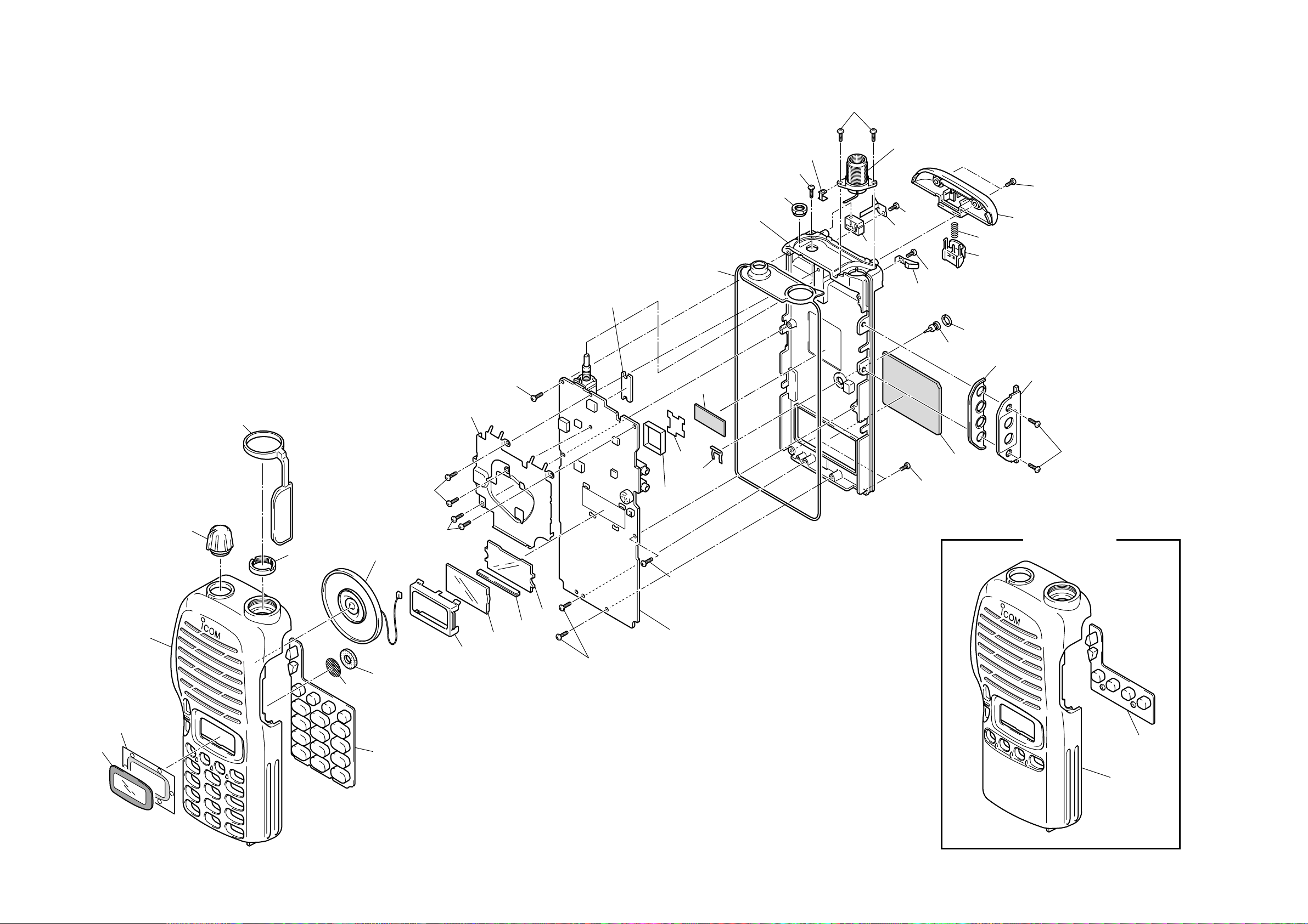
7 - 2
UNIT abbreviation (C): CHASSIS PARTS, (M): MAIN UNIT
MP4 (M)
MAIN unit
IC-F3GS parts
MP7 (C)
MP1 (C)
MP1 (C)
MP20 (C)
MP37 (C)
MP21 (C)
MP3 (M)
DS1 (M)
EP2 (M)
MP1 (M)
MP2 (M)
MP18 (C)
MP40 (C)
MP22 (C)
MP32 (C)
MP5 (M)
MP23 (C)
MP12 (C)
MP3 (C)
MP32 (C)
MP13 (C)
MP13 (C)
MP27 (C)
MP10 (C)
MP26 (C)
MP4 (C)
MP25 (C)
MP32 (C)
MP5 (C)
MP14 (C)
MP38 (C)
MP36 (C)
MP31 (C)
MP31 (C)
MP2 (C)
MP15 (C)
MP33 (C)
MP39 (C)
SP1 (M)
MP31 (C)
MP32 (C)
MP31 (C)
MP31 (C)
MP31 (C)
MP41 (C)
MP8 (C)
MP9 (C)
MP33 (C)
MP24 (C)
Page 25
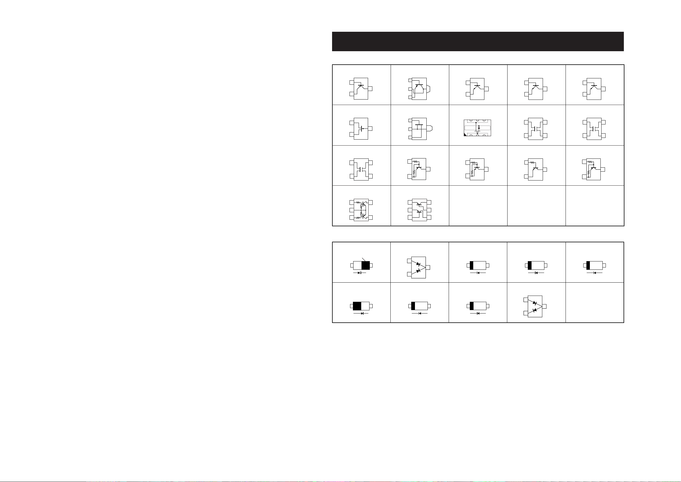
SECTION 8 SEMI-CONDUCTOR INFORMATION
8 - 1
2SC5085 Y
(Symbol: MCY)
2SK2974
(Symbol: K2974)
2SK1069 4
(Symbol: FJ4)
2SC4116 GR
(Symbol: LG)
2SA1577 Q
(Symbol: HQ)
2SB1132 R
(Symbol: BARB)
3SK239 A
(Symbol: XR)
2SC4215 O
(Symbol: QO)
2SK2973
(Symbol: K1)
DTC144 TU
(Symbol: 06)
DTC144 EUA
(Symbol: 26)
UN911 H
(Symbol: 6P)
XP1213
(Symbol: 9L)
3SK320
(Symbol: U7)
XP6501 AB
(Symbol: 5N)
3SK293
(Symbol: UF)
DTA144 EUA
(Symbol: 16)
•
TRANSISTOR AND FET’S
B
E
C
B
E
C
B
E
C
G
S
D
S
D
G
(top view)
S
D
S
G2
G1
D
S
G2
G1
B
E
C
B
E
C
B
E
C
E1
E2
B2
C1
B1
C2
B
E
C
D
G
S
B
E
C
B
C
E
E1
B1
B2
C1
C2
D
S
G2
G1
•
DIODES
MA77
(Symbol: 4B)
HVC350B
(Symbol: BO)
HVU350B
(Symbol: 4B)
MA2S077
(Symbol: S)
DAN202K
(Symbol: N)
1SV288
(Symbol: TJ)
MA8030 H
(Symbol: 3^0)
RB706F-40
(Symbol: 3J)
A
pink
C
A
C
MA8056 M
(Symbol: 5-6)
C
A1
A2
Page 26

SECTION 9 BOARD LAYOUTS
9 - 1
9-1 GENERAL AND EIA/TIA VERSIONS (EXCEPT W/N-TYPE)
• MAIN UNIT (TOP VIEW)
DS1
VHF
MC1
DS2
DS3
R204
R205 R155
R170
C215
C255
C256
R169
C233
C234
C295
R208
C211
R257
C286
C301
R175
R249
R151
R264
R186
R185
C293
R35
C55
C64
R89
C56
R90
R81
R80
R79
R84
R13
C26
C24
C25
R15
R12
R11
R10
C23
R14
R16
R177
C136 R114
R117
C137
R115
C217
C133
C134
R105
R176
R109
R93
R54
Q37
D33
D32
C75
C17
C251
C252
R162
R161
R163
C13
R7
R5
R3
R2
C205
C5
R9
W7
R210
R53
C52
C4C2
C1
R1
R52
C92C90
C81
C78
R222
R62
R57
C85
C93
C84
R64
R65
C73
C10
R108
C135
R116
C124
C243
R251
C179
R17
R97
C54
C51
C300
C303
R253
C111
C115
C117
L7
C290
C112
R244
C116
R83
R82
C159
R86
R85
R87
C19
C120
C122
R135
C156
C283
R88
C20
C121
C118
C280
R255
C289
R142
C14
C282
L28
C15
C22
C160
C119
Q19
Q20
C113
R134
C63
R45
R34
C46
C131
R125
C212
R168
R44
R30
R31
C148
C214 R113
C128
R112
R174
C299
R67
R66
C95
C96
R98
R107
C213
C50
Q11
Q25
J6
J6
C49
IC1
X3
X3
IC4
Q34
C294
L13
Q10
Q18
IC6
A
Q14
Q3
Q2
L32
Q1
D3
C21
L26
L6
L5
IC2
IC3
D4
D12
D27
Q31
L18
D10
D9
D8
D1
D2
L22
L15
R61
D11
Page 27

9 - 2
• MAIN UNIT (BOTTOM VIEW)
C277
R252
C138
R258
R143
FI2
FI1
J2
J3
MP5
S1
S3
S2
MP6
X1
S1 S3
Q21
Q22
L25
X1
IC10
IC7
IC8
C198
IC12
Q40
R236
R238
R237
S2
C158
C155
FI2
C174
C173
C72
C298
C281
L4
L2
L1
L16
L17
L24
D29
L31
C287
C285
C8
C3
C18
C76
R96
R95
R75
L20
L19
C105
C106
C109
C104
R94
R70
R72
C97
C98
C94
L29
C99
C169
L21
C101
C100
C102
C126
R178
R262
C108
C107
R160
R154
C288
C204
C82
C79
C80
C83
C86
C88
C87
C89
R59
R58
R63
C91
R100
R159
R187
C168
C165
C163
R144
R128
C164
C152
C151
R127
R122
R221
C248
C232
R181
R215
R216
C231
C193
C171
R126
R218
R101
C194
C195
R146 C197
R219
R220
C149
C146
C167
C166
R132
R99
R104
C110
FI1
C125
C278
C150
D26
Q16
Q15
Q36
D14
Q17
R226
R232
R182
L33
Q35
Q38
C129
Q12
C48
Q5
R20
R23
R21
C33
R22
R19
R261
R139
R141
C162
C67
C114
R260
C161
C65
C69
R50
R49
W8
C70
C123
C236
C244
R150
C71
R48
R51
D7
C66
C53
L8
R18
C27
R68
R69
C29
R77
C28
R26
C36
R25
C35
C38
D13
D5
C37
C39
L34
L10
C31
Q6
C30
C62
R41
C61
C42
R29
C218
C44
C41
C45
C47
R184
R152
R227
R202
C219
R123
C140
R121
C250
C216
R145
R120
C139
C228
R203
C227
R207
R224
R223
R229
R230
R231
R191
R192
C225
C222
C297
C296
C202
C245
C221
C201
R190
R225
R228
R234
R267
R153
R33
R32
C60
L14
C32
R28
R27
C34
C229
D28
Q32
Q8
L11
C153
IC5
C145
X2
C154
IC11
LV
D
C
BUSY
OPTION
B5386H
ICOM
F
J5
L12
Q7
Q4
C235
R209
L9
D6
Q13
C249
R198
R199
C200
R200
R196
R140
R265
R243
C209
C304
C132
C230
C302
C199
R195
R194
R193
R165
R131
R245
R246
R206
R213
R212
R240
R239
R235
R241
R242
R137
C223
C224
R171
R136
R266
C147
R130
R164
R147
R102
C196
C144
R148
R103
R211
R197
J5
J5
to the OPTIONAL unit
PTTIN
PTTOUT
MICOUT
MICIN
AUX
BUSY
MOWN
SIGOUT
OPT1
OPT2
OPT3
GND
OPV3
OPV2
OPV1
1
115
30 16
R268
GND5VVCC
MICMUTE
AFONOP
BEEPOUT
RXMUTE
DISCIN
AFOUT
REM
CCS
CIRQSOSI
SCK
IC13
Page 28

9 - 3
9-2 ETS/CEPT VERSION
• MAIN UNIT (TOP VIEW)
DS1
V H F
MC1
DS2
DS3
R204
R205 R155
R170
C215
R169
C233
C234
C295
R208
C211
R257
C286
C301
R175
R249
R151
R264
R186
R185
C293
R35
C55
C64
R89
C56
R90
R81
R80
R79
R84
R13
C26
C24
C25
R15
R12
R11
R10
C23
R14
R16
R177
C136 R114
R117
C137
R115
C217
C133
C134
R105
R176
R109
R93
R54
Q37
D33
D32
C75
C17
C251
C252
R162
R161
R163
C13
R7
R5
R3
R2
C205
C5
R9
W7
R210
R53
C52
C4C2
C1
R1
R52
C92C90
C81
C78
R222
R62
R57
C85
C93
C84
R64
R65
C73
C10
R108
C135
R116
C124
C243
R251
C179
R17
R97
C54
C51
C300
C303
R253
C111
C115
C117
L7
C290
C112
R244
C116
R83
R82
C159
R86
R85
R87
C19
C120
C122
R135
C156
C283
R88
C20
C121
C118
C280
R255
C14
R142
C289
C282
L28
C15
C22
C160
C119
Q19
Q20
C113
R134
C63
R45
R34
C46
C131
R125
C212
R168
R44
R30
R31
C148
C214 R113
C128
R112
R174
C299
R67
R66
C95
C96
R98
R107
C213
C50
Q11
Q25
J6
C49
IC1
X3
IC4
Q34
C294
L13
Q10
Q18
IC6
Q14
Q3
Q2
L32
Q1
D3
C21
L26
L6
L5
IC2
IC3
D4
D12
D27
L18
D10
D9
D8
D1
D2
L22
L15
R61
D11
C305
D34
Q31
J6
X3
A
C255C256
Page 29

9 - 4
• MAIN UNIT (BOTTOM VIEW)
C277
R252
C138
R258
R143
MP5
S1
FI2
FI1
S1 S3
Q21
Q22
L25
X1
IC10
IC7
IC8
C198
IC12
R236
R238
R237
S2
C158
C155
FI2
C174
C173
C72
C298
C281
L4
L2
L1
L16
L17
L24
D29
L31
C287
C285
C284
C8
C3
C18
C76
R96
R95
R75
L20
L19
C105
C106
C109
C104
R94
R70
R72
C97
C98
C94
L29
C99
C169
L21
C101
C100
C102
C126
R178
R262
C108
C107
R160
R154
C288
C204
C82
C79
C80
C83
C86
C88
C87
C89
R59
R58
R63
C91
R100
R159
R187
C168
C165
C163
R144
R128
C164
C152
C151
R127
R122
R221
C248
C232
R181
R215
R216
C231
C193
C171
R126
R218
R101
C194
C195
R146
C197
R219
R220
C149
C146
C167
C166
R132
R99
R104
C110
FI1
C125
C278
C150
D26
Q16
Q15
Q36
D14
Q17
R226
R232
R182
L33
Q35
Q38
C129
Q12
C48
Q5
R20
C306
R23
R21
C33
R22
R19
R261
R139
R141
C162
C67
C114
R260
C161
C65
C69
R50
R49
W8
C70
C123
C236
C244
R150
C71
R48
R51
D7
C66
C53
L8
R18
C27
R68
R69
C29
R77
C28
R26
C36
R25
C35
C38
D13
D5
C37
C39
L34
L10
C31
Q6
C30
C62
R41
C61
C42
R29
C218
C44
C41
C45
C47
R184
R152
R227
R202
C219
R123
C140
R121
C250
C216
R145
R120
C139
C228
R203
C227
R207
R224
R223
R229
R230
R231
R191
R192
C225
C222
C297
C296
C202
Q40
C245
C221
C201
R190
R225
R228
R234
R267
R153
R33
R32
C60
L14
C32
R28
R27
C34
C229
D28
Q32
Q8
L11
C153
IC5
C145
X2
C154
IC11
L12
Q7
Q4
C235
R209
L9
D6
Q13
C249
R198
R199
C200
R200
R196
R140
R265
R243
C209
C304
C132
C230
C302
C199
R195
R194
R193
R165
R131
R245
R246
R268
R206
R213
R212
R240
R239
R235
R241
R242
R137
C223
C224
R171
R136
R266
C147
R130
R164
R147
R102
C196
C144
R148
R103
R211
R197
J5
1
IC13
J3
J2
S3
X1
S2
MP6
LV
D
C
OPTION
B5571C
ICOM
F
J5
BUSY
J5
to the OPTIONAL unit
PTTIN
PTTOUT
MICOUT
MICIN
AUX
BUSY
MOWN
SIGOUT
OPT1
OPT2
OPT3
GND
OPV3
OPV2
OPV1
115
30 16
GND5VVCC
MICMUTE
AFONOP
BEEPOUT
RXMUTE
DISCIN
AFOUT
REM
CCS
CIRQSOSI
SCK
Page 30

9 - 5
9-3 W/N-TYPE
• MAIN UNIT (TOP VIEW)
DS1
VHF W/N
MC1
DS2
DS3
R204
R205 R155
R170
C215
R169
C233
C234
C295
R208
C211
R257
C286
C301
R175
R249
R151
R264
R186
R185
C293
R35
C55
C64
R89
C56
R90
R81
R80
R79
R84
R13
C26
C24
C25
R15
R12
R11
R10
C23
R14
R16
R177
C136 R114
R117
C137
R115
C217
C133
C134
R105
R176
R109
R93
R54
Q37
D33
D32
C75
C17
C251
C252
R162
R161
R163
C13
R7
R5
R3
R2
C205
C5
R9
W7
R210
R53
C52
C4C2
C1
R1
R52
C92C90
C81
C78
R222
R62
R57
C85
C93
C84
R64
R65
C73
C10
R108
C135
R116
C124
C243
R251
C179
R17
R97
C54
C51
C300
C303
R253
C111
C115
C117
L7
C290
C112
C307
C308
R244
R269
C116
R83
R82
C159
R86
R85
R87
C19
C120
C122
R135
C158
C156
C283
R88
C20
C121
C118
C280
R255
C289
R142
C14
C282
L28
C15
C22
C160
C119
Q19
Q20
C113
R134
C63
R45
R34
C46
C131
R125
C212
R168
R44
R30
R31
C148
C214
R113
C128
R112
R174
C299
R67
R66
C95
C96
R98
R107
C213
C50
Q11
Q25
J6
J6
C49
IC1
X3
IC4
Q34
C294
L13
Q41
Q10
Q18
IC6
A
Q14
Q3
Q2
L32
Q1
D3
C21
L26
L6
L5
IC2
IC3
D4
D12
D27
Q31
L18
D10
D9
D8
D1
D2
L22
L15
R61
D11
C255C256
Page 31

9 - 6
• MAIN UNIT (BOTTOM VIEW)
C277
R252
C138
R258
R143
FI2
FI1
J2
J3
MP5
S1
S3
S2
MP6
X1
S1
S3
Q21
Q22
L25
X1
IC10
IC7
IC8
C198
IC12
Q40
R236
R238
R237
S2
C155
FI2
C174
C173
C72
C298
C281
L4
L2
L1
L16
L17
L24
D29
L31
C287
C285
C8
C3
C18
C76
R96
R95
R75
L20
L19
C105
C106
C109
C104
R94
R70
R72
C97
C98
C94
L29
C99
C169
L21
C101
C100
C102
C126
R178
R262
C108
C107
R160
R154
C288
C204
C82
C79
C80
C83
C86
C88
C87
C89
R59
R58
R63
C91
R100
R159
R187
C168
C165
C163
R144
R128
C164
C152
C151
R127
R122
R221
C248
C232
R181
R215
R216
C231
C193
C171
R126
R218
R101
C194
C195
R146 C197
R219
R220
C149
C146
C167
C166
R132
R99
R104
C110
FI1
C125
C278
C150
D26
Q16
Q15
Q36
D14
Q17
R226
R232
R182
L33
Q35
Q38
C129
Q12
C48
Q5
R20
R23
R21
C33
R22
R19
R261
R139
R141
C162
C67
C114
R260
C161
C65
C69
R50
R49
W8
C70
C123
C236
C244
R150
C71
R48
R51
D7
C66
C53
L8
R18
C27
R68
R69
C29
R77
C28
R26
C36
R25
C35
C38
D13
D5
C37
C39
L34
L10
C31
Q6
C30
C62
R41
C61
C42
R29
C218
C44
C41
C45
C47
R184
R152
R227
R202
C219
R123
C140
R121
C250
C216
R145
R120
C139
C228
R203
C227
R207
R224
R223
R229
R230
R231
R191
R192
C225
C222
C297
C296
C202
C245
C221
C201
R190
R225
R228
R234
R267
R153
R33
R32
C60
L14
C32
R28
R27
C34
C229
D28
Q32
Q8
L11
C153
IC5
C145
X2
C154
IC11
LV
D
C
BUSY
OPTION
B5687A
F
J5
L12
Q7
Q4
C235
R209
L9
D6
Q13
C249
R198
R199
C200
R200
R196
R140
R265
R272
R273
R243
C209
R276
C309
C304
C132
C230
C302
C199
R195
R194
R193
R165
R131
R245
R246
R206
R213
R212
R240
R239
R235
R271
R241
R242
R270
R274
R137
C223
C224
R171
R136
R275
R266
C147
R130
R164
R147
R102
C196
C144
R148
R103
R211
R197
J5
1
R268
IC13
Q42
IC14
J5
to the OPTIONAL unit
PTTIN
PTTOUT
MICOUT
MICIN
AUX
BUSY
MOWN
SIGOUT
OPT1
OPT2
OPT3
GND
OPV3
OPV2
OPV1
115
30 16
GND5VVCC
MICMUTE
AFONOP
BEEPOUT
RXMUTE
DISCIN
AFOUT
REM
CCS
CIRQSOSI
SCK
ICOM
Page 32

10 - 1
SECTION 10
BC-137 OPTIONAL DESKTOP CHARGER INFORMASION
REF. NO. ODER NO. DESCRIPTION QTY .
MP1 8010018030 2338 case 1
MP2 8110007080 2338 cover 1
MP3 8930050920 2327 spacer 1
MP4 8930039620 Leg cushion (A) 4
MP5 8810008660 Screw BT M3 x 8 NI-ZU 1
[CHASSIS UNIT]
10-1 PARTS LIST
10-2 DISASSEMBLY INFORMATION
MP1 (C)
MP1 (M)
MP2 (C)
MP5 (C)
MP4 (C)
MP4 (C)
MP3 (C)
MAIN unit
MP4 (C)
S.=Surface mount
REF. NO. ODER NO. DESCRIPTION QTY.
[MAIN UNIT]
Q1 1520000650 S.TRANSISTOR 2SB1201-S-TL 1
Q2 1590000480 S.TRANSISTOR RN2402 (TE85R) 1
Q3 1590000510 S.TRANSISTOR RN1409 (TE85R) 1
Q4 1530001950 S.TRANSISTOR 2SC2712-GR (TE85R) 1
D1 1750000550 S.DIODE 1SS355 TE-17 1
D2 1750000020 S.DIODE 1SS184 (TE85R) 1
D3 1790000950 S.ZENER MA8056-M (TX) 1
R1 7030010000 S.RESISTOR
MCR10EZHF 24R0 Ω (240)
1
R2 7030010000 S.RESISTOR
MCR10EZHF 24R0 Ω (240)
1
R3 7030000190 S.RESISTOR MCR10EZHJ 27 Ω (270) 1
R4 7030000500 S.RESISTOR MCR10EZHJ 10 kΩ 1
R5 7030000500 S.RESISTOR MCR10EZHJ 10 kΩ 1
R6 7030000190 S.RESISTOR MCR10EZHJ 27 Ω (270) 1
R7 7030001740 S.RESISTOR MCR10EZHJ 2 kΩ 1
R8 7030001740 S.RESISTOR MCR10EZHJ 2 kΩ 1
R9 7030000590 S.RESISTOR MCR10EZHJ 56 kΩ 1
R10 7030000500 S.RESISTOR MCR10EZHJ 10 kΩ 1
R11 7030000380 S.RESISTOR MCR10EZHJ 1 kΩ 1
C1 4030001150 S.CERAMIC GRM40 F 104Z 25PT 1
C2 4030001150 S.CERAMIC GRM40 F 104Z 25PT 1
C3 4030001150 S.CERAMIC GRM40 F 104Z 25PT 1
C4 4030001150 S.CERAMIC GRM40 F 104Z 25PT 1
J1 6510021470 CONNECTOR HEC0470-01-230 1
J2 6510021470 CONNECTOR HEC0470-01-230 1
DS1 5040001390 LED TLG124A 1
W1 7030003970 S.JUMPER MCR18EZHJ JPW (000) 1
EP1 0910052602 PCB B 5493B 1
EP2 6910012240 SPACER TLE60-05 1
MP1 8930051340 2338 TERMINAL 3
Screw abbreviations BT: Self-tapping
NI :Nickel
NOTE: (C) : CHASSIS
(M) : MAIN UNIT
CONVENIENT:
BC-137 is connectable max. 6 pieces in parallel.
When connect BC-137 in parallel, JIG cable (as shown
below) is required.
AC adaptor (BC-122)
or DC power supply
JIG cable
BC-137
J1J2
BC-137
J1J2
• CONNECTION
BC-137
J1J2
–
( GND)
+
( 13.8 V)
• JIG CABLE
AP-301 (Order No: 5610000010)
Max. 6 pieces of BC-137
Page 33

10 - 2
10-3 VOLTAGE DIAGRAM
10-4 BOARD LAYOUT
J2
J1
Q1
2SB1201 S
R5 10 k
D2 1SS184
R1 24
R2 24
W1
CHARGE+
GND
TEMP
DS1 TLG124A
C4
0.1
R6
27
C2
0.1
R7
2 k
R8
2 k
R9
56 k
R10
10 k
R4 10 k
Q4
2SC2712 GR
C3
0.1
Q2
RN2404
R3
27
D1
1SS355
Q3
RN1409
D3
MA8056 M
R11
1 k
C1
0.1
13.80 V
12.49 V
12.47 V
11.82 V
11.80 V
5.62 V
0 V
0.74 V
0.73 V
0 V
13.77 V
13.63 V
12.46 V
0.23 V
0.22 V
7.20 V
8.01 V
7.98 V
C4
C1
R1
R9
R10
R5
C2
R7
R8
R6
D1
Q1
W1
R2
R11
R4
Q2
Q3
Q4
D3
D2
R3
C3
Page 34

11 - 1
SECTION 11 BLOCK DIAGRAM
ANT
LPFLPF
ANT
SW
D1 MA77
D2 MA77
D8 MA77
Q1 2SK2974Q2 2SK2973Q3 2SC5085 Y
D3 MA77
D4 MA77
PLL IC
Q4 2SC4215 OQ6 2SC4215 O
IC1 UPD3140GS
VCO
Q7 2SC5085 Y
Q8 2SC5085 Y
REF
OPTION UNIT
J5 AXN330C038
2TONE or 5TONE
PTT
MIC
AF
REG
AF
AMP
PTT
CONT
Q17 UN911H
VCC
IC5 TA7368F
FRQCON
DBAL
Q15 2SB1132 R
Q16 XP6501 AB
D26 DAN202K
DEV
MIC, AF, PTT, MMUT
RMUT, AFONOP
SIGOUT
IF DET IC
DET
IC2 TA31136FN(D)
Q5 2SC4215 O
Q14 2SC4215 O
Q41 2SC4116 GR A only
Q34 2SK1069 4
SQL
BPF
BPFBUFF
Q10 2SC4116 GR
(30.6MHz)
APC
Q12 3SK293
Q13
3SK239A [OTHER]
3SK320 B
TXC
PWR
DET
PWR
AMP
PRE
DRIVE
TX/RX
SW
BUFFBUFFBUFF
LOOP
FIL
W/N SWITCHING
CIRCUIT
BUFF
BUFF
BPF BPF BPF
D/A
RF
AMP
IF
AMP
D32 RB706F-40
D33 RB706F-40
D9 HVU350B
D10 HVU350B
D11 HVU350B
D12 HVU350B
IC3A NJM2902V
Q37 DTA144EU
IC10
M62363FP-650C
RESET
LPF
LPF
BUFF
+5
CPU
VCC
IC11 S-80942ANMP-DD6
IC6
TK11250BM [OTHER]
NJM2870 A
S5C
S5
CONT
CPU5
NWC
Q20 DTA144EU
REG
S5
S5
Q21 2SA1577 Q
IC3B NJM2902V
HPF
LPF
IC4 BU4066BCFV
SD
NOIS
CPU5
Q18 2SB1132 R
Q19 XP6501 AB
5V
OPT
BUFF
D/A
AF OUT
SP
Q31 DTC144TU
D27 RB706F-40
IC10
M62363FP-650C
VR
MIC JACK
SP JACK
EXT.MIC
SP
BATT
GND
BDET
VCC
CLONE
POWER SW
PRE
ENPHA
MIC
AMP
ANALOG
SW
REG
R5
REG
T5
R5
T5
Q22 2SA1577 Q
IC3D NJM2902V
IC3C NJM2902V
CTCSS
TONE
RMUT
MMUT
Q35 2SC4116 GR
DTMF
MTONE
CTCSS
DTCS
Q36 2SC4116 GR
R5C
T5C
IC12 NJM2904V
IC8 HD6433876B50H
CPU
LCD
KEY
MATRIX
EEPROM
IC7
HN58X2432TI [OTHER]
HN58X2464TI H
X2 CR-663
(9.2 MHz)
T3, T4
T1, T2
T4
COMMON LINE
TX LINE
RX LINE
X1
CR-664A [OTHER]
CR-671A A, D
(15.3 MHz)
FI2
SFPC450G [OTHER]
SFPC450E C, G
SFPC450D E
CFWC450F A
(450kHz)
FI1
FL-311 [OTHER]
FL-312 C
FL-333 F, G
FL-334 E
(31.05MHz)
NOTE
A: W/N-type B: ETS/CEPT version C: W-type of [GEN] D: EIA/TIA version
E: W-type of ETS/CEPT version F:
N-type of ETS/CEPT version
G: M (20 kHz)-type H: 100 channel version
R5
Q403 2SC5107 O
BUFF
Page 35

R
2
4
KS4
P53/WKP3/SEG4
39
PE /SEG /CL
87
:
N
—
SECTION 12 VOLTAGE DIAGRAM
to Optional unit
MC1
KUC3523-040245
MIC
PTT
SWITCH
J2
HSJ1122-010010
EXT.MIC
EXT.SP
J3
HSJ1456-01-220A
BATT
GND
BDET
J5
AXN330C038
16
SCK
15
OPV1
17
SI
14
OPV2
18
SO
13
OPV3
19
CIRQ
12
GND
20
CCS
11
OPT3
21
REM
10
OPT2
22
AFOUT
9
OPT1
23
DISCIN
8
SIGOUT
24
RXMUTE RMUTE
7
MOWN
25
BEEPOUT
6
BUSY
26
AFONOP
5
AUX
27
MICMUTE MMUTE
4
MICIN
28
VCC
3
MICOUT
29
5V
2
PTTOUT
30
GND
1
PTTIN
D34
MA8056 M
J6
BM02B-ASRS-TF
1
2
S3
JPM1990-2711R
VOL/ PWR
SWITCH
C282
470 P N
0.001 [OTHER]
E only
SP
R144
22 K
C163
0.001
R143
TP76N00N-15F-10KA-2251
VOLOUT
VOLIN
A
(VR)
C165
0.001
AFOUT
SP
CLONE
C223
0.01
C167
47 P
C283
0.001
C164
0.001
MIC
C224
0.01
C166
0.001
C168
0.001
C173
47
R142
100
VOLIN
VOLOUT
HV
OPT
MIC
AFOUT
C169
0.001
C305
470 P
E only
MIC
VOLIN
VOLOUT
AFOUT
MIC
SP
BUSY
PTT
CPU5
CPU55VT5R5S5
VCC
R132
470
VCC5VT5R5S5
VCC
D27
RB706F-40
4.92 V
AFOUT
DISCIN
VCC
T5
R5
S5
5V
R5
S5
R5
S5
VCC
CPU5
TX: 4.84 V
RX: 0 V
CPU5
VCC
5V
R5
S5
TX: 4.97 V
RX: 0.03 V
T5
Q22
2SA1577 Q
TX: 0.85 V
RX: 5.01 V
CPU5
S5
T5
R5
R174
15 k
Q31
DTC144TU
C299
470 P
D
C147
0.047
R141
4.7 k
CLIN
T5C
CLOUT
4.96 V
C154
10
R140
100 k
C162
0.01
BDET
Q17
UN911H
R130
100 k
TX: 0 V
RX: 5.01 V
R260
10 k
BDET
AFOUT
DISCIN
VCC
T5
R5
S5
5V
R5
S5
R5
S5
VCC
13
12
IC3D
NJM2902V
R103
12 k
D14
MA77
C196
470 P
4.5 V
1.2 V
4.8 V
4.4 V
1.4 V
1.0 V
R115
120 k
C135
180 P
VCC
CPU5
R215
100 k
R216
100 k
C195
56 P
C193
8 P
R232
1 k
R165
100 k [F3GS] only
14
C231
0.1
X2
CR-663
R101
1 M
R226
1 k
R243
1 M
R117
1.5 k
R116
1 k
C137
0.027 [OTHER]
0.033 I
1.94 V
R99
12 k
R100
1.8 k
VOLOUT
AFOUT
R182
NTCCM20124AG473JCT
R181
C232
100 k
0.1
R102
10
C194
15 P
R241
R242
1 M
1 M
R194
100 k
R193
100 k
TX: 0 V
RX: 4.62 V
C129
15
R195
100 k
1.94 V
R178
3.9 k
CTCIN
REMO
TEMPS
TX: 0 V
RX: 3.96 V
AFONOP
BDET
VIN
XIN
XOUT
RESET
CSIFT
SCK
SI
SO
DAST
CLIN
CLOUTCLOUT
PLST
NOIS
CIRQ
BUSY
CCS
OPT1
OPT2
OPT3
R235
680 k
D26
DAN202K
AFON
C302
0.1
C212
0.01
C213
2.2
C214
0.033
R170
10 k
R148
100 k
5
CD
4
C230
0.022
1
A0
2
A1
3
A2
4
VSS
R234
10 k D
22 k [OTHER]
R231
22 k
R230
56 k
R229
180 k
R227
47 k
C219
0.0082
R97
220 k
R98
180 k
R107
150 k
R113
68 k
CTDA2
CTDA1
CTDA0
DUSE
C197
0.1
C136
0.0056
C144
0.001
SCK
SI
SO
DAST
CLIN
PLST
NOIS
CIRQ
BUSY
CCS
OPT1
OPT2
OPT3
DTCS
CTCSS
R114
22 k [OTHER]
33 k I
R159
100 k
R146
12 k
R147
12 k
R164
100 k [F3GT] only
CPU5
VCC
5V
C202
0.01
C222
0.1
R192
22k
R95
1 M
6
5
IC3B
NJM2902V
5.02 V
T1
T2
T3
T4
DAST
SCK
SO
IC12A
NJM2904V
3
2
C225
0.0047 I
0.0068 [OTHER]
7
R96
47 k
R152
R153
470 k
470 k
TONE
Q36
2SC4116 GR
C248
0.01
R211
120 k
8
1
4
R212
68 k
C286
0.0022
C201
0.1
R154
470 k
R257
1
R268
100 k
MMUT
R198
18 k
R197
220 k
Q40
XP1213
TX: 5.0 V
RX: 0.01 V
R5C
R150
470
C244
0.01
R220
270 k
R218
120 k
R221
330 k
IC14
TC7S66FU
D only
IC13
TC7S66FU
C198
2.2
4
5
IC4
BU4066BCFV
1
I/O
2
O/I
3
O/I
4
I/O
5
CONT.B
6
CONT.C
7
VEE
IC10
M62363FP-650C
1
VIN1
2
VOUT1
3
VOUT2
4
VIN2
5
VDD
6
LD
7
CLK
8
DI
9
VIN3
10
VOUT3
11
VOUT4
VIN412VIN5
C236
0.01
REM
DTMF
MTONE
R219
120 k
5
4
R199
47 k
C200
0.033
R200
47 k
0 V
VDD
CONT.A
CONT.D
C309
0.1
D only
5
1
2
3
2
1
14
13
12
11
I/O
10
O/I
9
O/I
8
I/O
C131
0.01
VOLIN
VOLOUT
AFOUT
VIN8
VOUT8
VOUT7
VIN7
GND
RESET
VDAREF
DO
VIN6
VOUT6
VOUT5
R276
10 k
D only
Q42
DTC144EU
D only
4
R275
3
4.7 k
D only
1
3
IC12B
NJM2904V
6
5
R267
47 k R
100 k [OTHER]
2
R206
470 k
R168
10 k
R44
10 k R
R112
1 M
C128
1
RMUT
SQLIN
C123
NWC
3.8 V
FRQCOM
CTCIN
R213
470
0.001
DBAL
CTCSS
DEV
ESDA
CTCSS
R228
10 k
C250
0.01
R224
8.2 k D
22 k A
27 k [OTHER]
C216
0.1 [OTHER]
0.22 D
DET5VCTCIN
ESCK
R225
100 k
CTCSS
DTCS
Q35
2SC4116 GR
R207
47 k
24
23
22
21
20
19
18
17
16
15
14
13
7
18 k [OTHER]
20 k A, D
R169
10 k R
12 k [OTHER]
TONE
CTCSS
SIGOUT
5.01 V
L33
1.0 H
IC11
S-80942ANMP-DD6
1
OUT
2
VDD
VSS3NC
IC7
HN58X2432TI [OTHER]
HN58X2464TI Q
8
VCC
7
WP
6
SCL
5
SDA
C245
0.01
1.5 V
0.4 V
1.2 V
0.4 V
C227
0.047 D
0.1 [OTHER]
Q38
DTC144EU
R202
47 k
R203
47 k
C228
820 P
R177
C132
R266
5.06 V
15 k
C
C161
0.01
C304
0.047
R137
100
R261
10 k
0.0056
MICOUT
C174
22
R134
2.2 k
P0
P1
P2
P3
R105
390 [OTHER]
470 I
C133
0.1
TONE
Q18
2SB1132 R
C159
470 P
S2
JPM1990-2711R
R104
100 k
R125
27 k
Q19
XP6501 AB
456
5.01 V
Q20
DTA144 EU
321
4.44 V
R135
10 k
10
R131
470
TX: 3.69 V
RX: 5.01 V
C209
0.1
MICIN
Q21
2SA1577 Q
C294
33
R139
4.7 k
TX: 5.01 V
RX: 0.86 V
R5C
UP
DN
23
1
56
4
89
7
0#
*
IC3C
NJM2902V
9
C134
220 P
R108
150 k
C148
0.01
C160
0.01
R239
1 k
S1
JPM1990-2711R
R109
10 k
1 k
8
VOLIN
VOLOUT
AFOUT
BEEPOUT
C158
10
S5C
R238
1 k
R240
1 k
C124
C217
0.01
0.1
R176
3.9 k
R171
47 k
0.12 V
IC6
TK11250BM [OTHER]
C156
0.01 D
0.1 [OTHER]
S5
T5
R5
KR0
KR1
KR2
KR3
KS4
KS3
KS2
KS1
KS0
C249
0.01
S1
C125
0.0022
NJM2870 D
T5
R5
R93
27 k
C215
0.1
4
VOUT
GND
N. BYPASS
3
2
R190
22 k
C221
0.039
5
1
DET
C126
0.0027
VIN
CONT
C155
10
R191
22 k
DTMF
3.8 V
0.8 V
R94
1 M
Q15
2SB1132 R
R120
68 k
R145
1 M
TX: 0 V
RX: 4.99 V
1
PB0/AN0
2
AVSS
3
TEST
4
X2
5
X1
6
VSS
7
OSC1
8
OSC2
9
RES
10
NMI
11
P20/IRQ4/ADTRG
12
P21/SCK1
13
P22/SI1
14
P23/SO1
15
P24/SCK3
16
P25/RXD
17
P26/TXD
18
P27/IRQ0
19
P17/IRQ3/TMIF
20
P16/IRQ2
21
P15/IRQ1
22
P14
23
P13/TMIG
24
P12/TMOFH
25
P11/TMOFL
CONT
R196
100 k
C199
0.1
R265
100 k
C139
0.1
VCC
R121
1 k
LVINSDREMO
100999897969594939291908988
P81/AN1
P82/AN2
P83/AN3
P10/TMOW
VSS
V3V2V1
26272829303132333435363738
R272
100 k
D only
R273
100 k
D only
BDET
PTT
P84/AN4
P85/AN5
P86/AN6
VCC
Q16
XP6501
456
321
C140
0.1
CTCIN
CPU5
CPU5
VTREF
AVREF
P87/AN7
PA3/COM4
PA2/COM3
PA1/COM2
VOLMI
7.23 V
TX:
RX
CPU5
DTMF
MTONE
AVCC
TONED
TONEM
IC8
HD6
PA0/COM1
P50/WKP0/SEG1
PE3/SEG52/CL1
P51/WKP1/SEG2
P52/WKP2/SEG3
12 - 1
COM4
COM3
COM2
COM1
Page 36

5
AFOUT
3
0
R
7
V
T
b
DISCIN
VCC
T5
R5
S5
5V
R5
S5
VCC
Q15
4 V
CTCIN
REMO
TEMPS
TX: 0 V
RX: 3.96 V
AFONOP
BDET
VIN
XIN
XOUT
RESET
CSIFT
SCK
SI
SO
DAST
CLIN
CLOUT
PLST
NOIS
CIRQ
BUSY
CCS
OPT1
OPT2
OPT3
R235
680 k
R120
68 k
D26
DAN202K
AFON
C302
0.1
10
11
12
13
14
15
16
17
18
19
20
21
22
23
24
25
R196
100 k
2SB1132 R
R145
R121
C139
1 M
1 k
0.1
TX: 0 V
RX: 4.99 V
R265
100 k
LVINSDREMO
100999897969594939291908988878685848382818079787776
P81/AN1
P82/AN2
P83/AN3
1
PB0/AN0
2
AVSS
3
TEST
4
X2
5
X1
6
VSS
7
OSC1
8
OSC2
9
RES
NMI
P20/IRQ4/ADTRG
P21/SCK1
P22/SI1
P23/SO1
P24/SCK3
P25/RXD
P26/TXD
P27/IRQ0
P17/IRQ3/TMIF
P16/IRQ2
P15/IRQ1
P14
P13/TMIG
P12/TMOFH
P11/TMOFL
P10/TMOW
VSS
V3V2V1
26272829303132333435363738394041424344454647484950
CONT
R272
100 k
D only
C199
0.1
R273
100 k
D only
V
.62 V
78
k
k
BDET
PTT
P84/AN4
P85/AN5
P86/AN6
456
321
C140
0.1
CTCIN
CPU5
AVREF
P87/AN7
VCC
PA3/COM4
PA2/COM3
COM4
COM3
Q16
XP6501 AB
CPU5
DTMF
VTREF
PA1/COM2
COM2
COM1
VOLMIN — VOLMAX
7.23 V — 7.07 V
TONED
PA0/COM1
R122
2.7 k
C145
R123
10
3.3 k
TX: 0 V
RX: 3.96 V
CPU5
MTONE
SEG22
SEG21
SEG20
SEG19
AVCC
TONEM
PD7/SEG48
PD6/SEG47
PE0/SEG49/M
PE1/SEG50/DO
PE3/SEG52/CL1
PE2/SEG51/CL2
IC8
HD6433876B50H
P50/WKP0/SEG1
P51/WKP1/SEG2
P52/WKP2/SEG3
P53/WKP3/SEG4
P54/WKP4/SEG5
P55/WKP5/SEG6
P56/WKP6/SEG7
P57/WKP7/SEG8
KS4
KS3
KS2
KS1
KS0
C146
0.001
SEG18
SEG17
SEG16
SEG15
PD5/SEG46
PD4/SEG45
PD3/SEG44
P60/SEG9
P61/SEG10
P62/SEG11
KR3
KR2
KR0
KR1
C171
0.1
VOLOUT
CPU5
SEG14
SEG13
PD2/SEG43
PD1/SEG42
PD0/SEG41
P97/SEG40
P96/SEG39
P95/SEG38
P94/SEG37
P93/SEG36
P92/SEG35
P91/SEG34
P90/SEG33
P87/SEG32
P86/SEG31
P85/SEG30
P84/SEG29
P83/SEG28
P82/SEG27
P81/SEG26
P80/SEG25
P77/SEG24
P76/SEG23
P75/SEG22
P74/SEG21
P73/SEG20
P72/SEG19
P71/SEG18
P70/SEG17
P67/SEG16
P63/SEG12
P64/SEG13
P65/SEG14
P66/SEG15
S1
R126
10 k
C149
0.1
R274
10 k D only
1.5 V (Light ON)
VCC
MMUT
RMUT
75
74
73
72
71
70
69
68
67
66
65
64
63
62
61
60
59
58
57
56
55
54
53
52
51
IC5
TA7368F
1
NC
2
VCC
3
NC
4
VIN
RIPPLE5NF
DS2
LNJ310M6URA
DS3
LNJ310M6URA
Q25
2SC4116 GR
R204
3.3 k
C256
0.001
R246
R245
100 k
100 k
R205
1.5 k
POUT
PWGND
PREGND
PHASE
R155
100
R237
1 k
R236
1 k
R127
33
3.31 V
10
9
8
7
6
C150
C151
10
47 P
C255
0.001
SEG12
SEG11
SEG10
SEG9
SEG8
SEG6
SEG5
SEG4
SEG3
SEG2
SEG1
SEG7
UNLK
CTDA2
CTDA1
CTDA0
ESDA
ESCK
AFON
TXC
T5C
R5C
C296
0.001
S5C
DUSE
MMUT
RMUT
C297
0.001
NWC
OPV2
OPV3
OPV1
C152
0.047
C153
100
R128
10
AFOUT
SQLIN
AFOUT
DISCIN
VCC
T5
R5
S5
5V
R5
S5
AFOUT
DISCIN
AFOUT
DBAL
FRQCON
PLST
SCK
SO
UNLK
LVIN
DEV
C51
47 P
SQLIN
DISCIN
AFOUT
R5
S5
R223
100 k
C293
0.1
S55VR5
S5
R5
R90
C56
680 k
0.01
Q10
2SC4116 GR
R88
33 k R
39 k [OTHER]
R87
2.2 k I
470 [OTHER]
C62
9 P C
18 P B
R51
100 k
R89
1.2 k
L13
1.0 H
C53
18 P
C72
1
C71
0.1
L14
47 nH B
82 nH C
C61
12 P C
18 P B
TX: 0 V
RX: 3.47 V
C65
2 P
C66
18 P
R48
1 k A, O
10 k [OTHER]
R50
470 k
C70
0.01
W8
ERJ3GE-JPW
C60
0.001
C67
10 P
L25
1.0 H
C121
220 P I
330 P [OTHER]
R86
47 k I
82 k [OTHER]
C122
220 P I
330 P [OTHER]
R136 100
C69
R49
68 P
47 k
D7
1SV288
C55
0.01
R41
47 B
100 C
FI2
SFPC450E G, P
SFPC450D J
SFPC450G [OTHER]
CFWC450F D
OI
SEG1
SEG2
SEG3
SEG4
SEG5
SEG6
SEG7
SEG8
SEG9
SEG10
SEG11
SEG12
SEG13
SEG14
SEG15
SEG16
SEG17
SEG18
SEG19
SEG20
SEG21
SEG22
COM1
COM2
COM3
COM4
C64
4 P
C120
0.1
R35
680
R84
390
R85
1.5 k
F (DET)
X1
CR-664A [OTHER]
CR-671A D, H
C63
39 P
1
VCC1
GND1
2
IN1
3
ENB
VCC2
4
CLK
5
DATA
6
T1
7
LOK
GND2
8
CP1
9
FI1
FO110FO2
IC1
UPD3140GS
TX: 1.92 V
RX: 1.98 V
R34
10
C49
0.68
TX: 0.85 V
RX: 0.47 V
TX: 0 V
RX: 3.64 V
IC2
TA31136FN (D)
1
OSCIN
2
OSCOUT
3
MIXOUT
4
VCC
5
IFIN
6
DEC
7
FILOUT
FILIN8AFOUT
C118
C119
0.01
1
1
COM4
2
COM3
3
COM2
4
COM1
5
SEG1
6
SEG2
7
SEG3
8
SEG4
9
SEG5
10
SEG6
11
SEG7
12
SEG8
13
SEG9
14
SEG10
15
SEG11
16
SEG12
17
SEG13
18
SEG14
19
SEG15
20
SEG16
21
SEG17
22
SEG18
23
SEG19
24
SEG20
25
SEG21
26
SEG22
27
COM1
28
COM2
29
COM3
30
COM4
CP2
IN2
XB
XO
FI2
R45
100
20
19
18
17
16
XI
15
14
13
12
11
DS1
LM-7045B
C54
0.001
R33
2.2 k
C48
2.2
MIXIN
GND
N-REC
N-DET
RSSI
IFOUT
QUAD
C303
0.001
16
15
14
13
12
11
10
9
CP1
(LV check ponit)
C290
15 P
R264
68 k [OTHER]
150 k R
C295
0.001
R244
100 k
C117
0.001
VCC
D13
HVC350B
R262
1 k [OTHER]
1 G
T5
4.72 V
1.44 V
C37
2 P
R26
4.7 k
C36
0.001
C38
2.5 P
R77
10 E
100 [OTHER]
C109
0.001
VCC
T5
C300
0.001
R27
470
R25
4.7 k
5V
C107
0.001
R75
120 [OTHER]
150 A
R28
3.57 V
100
C39
0.001
Q8
2SC5085 Y
L34
2.2 H
C35
0.001
Q7
2SC5085 Y
C106
39 P E
47 P G
56 P [OTHER]
TX: 0 V
RX: 0.53 V
C105
0.01
3.58 V
R22
68 k
C33
0.001
C34
0.5 P
S5
R5
L20
0.47 H [OTHER]
0.56 H E, G
Q13
3SK239A [OTHER]
3SK320 E
C104
R72
0.001
10 k
R70
4.7 k M, P
10 k A
56 k F
100 k [OTHER]
R23
100
L10
0.1 H C
0.15 H B
C32
0.001
C31
5 P
Q6
2SC4215 O
0 V
C102
15 P
L29
0.1 H
R20
68 k
0 V
L21
47 nH
C101
56 P [OTHER]
22 P A
C100
39 P [OTHER]
22 P A
R21
100
3.59 V
L9
0.1 H C
0.15 H B
C30
22 P
Q5
2SC4215 O
1LO
R68
4.7 k
C98
5 P [OTHER]
3 P N
L19
56 nH C
68 nH B
R18
C29
39 k
0.001
C28
12 P
Q4
2SC4215 O
R69
100
C99
0.001
C97
5 P [OTHER]
4 P N
D12
HVU350B
C96
180 P
T4
R67
100 k
R19
100
R66
100 k
C95
0.001
4.03 V
L8
0.1 H
TX: 0.7 V
RX: 0.73 V
C27
18P
D11
HVU350B
R17
1 k
C94
1 P
3.37 V
R64
100 k
C93
0.001
R65
100 k
C26
0.001
TX: 0 V
RX: 4.76 V
C92
100 P
C91
5 P
T3
D4
MA77
D3
MA77
C90
0.001
R15
100
R14
4.7 k
R16
1
S5
R5
R61
47
TX: 0 V
RX: 2.43 V
R187
1 k B
100 k C
C234
0.001
C233
0.001
R32
560
NOIS
C114
0.033
R185
1 k
5V
R186
47 k
R208
10 k
C116
82 P I
120 P [OTHER]
C113
0.001
SD
Q34
2SK1069 4
R184
10 k
C47
0.1
C235
0.1
R82
2.2 k [OTHER]
3.9 k I
R83
470
C112
0.001
R5
R175
1 k
C211
0.1
TX: 0.97 V
RX: 1.03 V
TX: 0 V
RX: 3.24 V
C218
0.001
Q32
DTC144EU
C229
0.001
X3
CDBC450CX24
R269
2.7 k D only
C307
0.01 D only
Q41
2SC4116 GR D only
C308
DET
0.01 D only
R31
1 k
R151
47 k
TX: 5.03 V
RX: 0.05V
D28
MA77
R209
100 k
R81
1.5 k [OTHER]
560 J
R253
470
C115
0.01
C46
0.001
L12
2.7 H
R29
1 k
C42
0.001
R79
560 except J
1.2 k G
Q14
2SC4215 O
R271
47 k D only
C301
0.001
D6
MA2S077
C44
0.001
TX: 1.39 V
RX: 2.47 V
TX: 0 V
RX: 2.3 V
C111
0.01
R80
100 k
R270
47 k D only
S5
Q11
XP6501 AB
6
5
4
R30
4.7 k
L11
MC152-E558CN-100024
C45
82 P C
180 P B
C41
30 P B
39 P C
R249
47 k
TX: 0 V
RX: 4.58 V
FI1 (31.05MHz)
FL-311 [OTHER]
FL-312 G
FL-333 M, P
FL-334 J
C110
1 P G
3.5 P J
9 P [OTHER]
NWC
1
2
3
C50
10
D5
HVC350B
C108
0.01
NOTE
A: L-band of ETS/CEPT version B: L-band C: H-band D: W/N-type E: E
G: W-type of [GEN] H: EIA/TIA version I: N and W/N-type J: W
L: H-band of [GEN] and EIA/TIA version M: N-type of ETS/CEPT version N: H-
P: M (20 kHz)-type Q: 100 channel version R: N-type
C24
0.001
C25
6 P
R11
1.2 k
TX: 0.8 V
RX: 0 V
C89
0.001
C88
0.001
R13
33
R12
3.3 k
L18
56 nH C
68 nH B
Q12
3SK293
TX: 0 V
RX: 4.76
C87
0.01
C2
0.0
4
Page 37

19
0
L8
0.1 H
C4215 O
350B
66
00 k
7
k
95
001
4.03 V
3.37 V
TX: 0.7 V
RX: 0.73 V
C27
18P
R17
1 k
C94
1 P
D11
HVU350B
R64
100 k
C93
0.001
R65
100 k
C26
0.001
TX: 0 V
RX: 4.76 V
C92
100 P
C91
5 P
T3
D4
MA77
D3
MA77
C90
0.001
R15
100
R14
4.7 k
R16
1
S5
R5
R61
47
TX: 0 V
RX: 2.43 V
R187
1 k B
100 k C
C24
0.001
C25
6 P
R11
1.2 k
TX: 0.8 V
RX: 0 V
C89
0.001
C88
0.001
R13
33
R12
3.3 k
L18
56 nH C
68 nH B
Q12
3SK293
TX: 0 V
RX: 4.76 V
C87
0.01
L7
0.1 H
Q3
2SC5085 Y
C22
27 P
C23
0.001
R222
10 k [OTHER]
15 k A
R59
470
TX: 4.62 V
RX: 0.04 V
R10
27 K
68 A
82 [OTHER]
C138
0.001
L28
82 nH
R252
100 k
C20
0.001
C280
30 P A
47 P [OTHER]
R7
100
C17
0.001
R258
TX: 0 V
33 k
RX: 3.57 V
C277
1.5 P [OTHER]
2 P G
L17
56 nH C
68 nH B
T2
VCC
L6
39 nH
C86
5 P
R63
100 k
R255
56
Q2
2SK2973
TX: 2.17 V
RX: 0.53 V
R9
10 k
C298
4.7
D10
HVU350B
R62
100 k
C85
180 P
C84
0.001
L26
3225 H
C19
0.001
C15
82 P
C83
1 P
C21
4.7
R5
22
D9
HVU350B
R57
100 k
C82
0.001
C14
0.001 [OTHER]
0.01 N
Q1
2SK2974
TX: 2.16 V
RX: 0.53 V
C13
0.001
C18
0.001
C80
2 P B
3 P C
L16
C81
56 nH C
100 P
68 nH B
R58
100 k
L5
10.5 nH
L32
15 nH [OTHER]
17 nH E
C79
5 P
C78
10 PD8MA77D2MA77
T1
C289
0.01
L31
7.5 nH
C285
56 P K
47 P [OTHER]
39 P N
C251
0.001
L22
50 nH
C281
0.001
TX: 0.83 V
RX: 0.01 V
C52
22 P
R3
2.2 k
R162
22 k
C10
0.001
L4
50 nH
C287
20 P [OTHER]
27 P A
D33
RB706F-40
L15
50 nH
C76
8 P
C288
0.001
C278
20 P [OTHER]
27 P A
R161
22 k
W7
ERJ3GE-JPW
C73
0.1
1
IC3A
NJM2902V
D29
MA8030 H
C204
0.001
C205
0.001
R2
2.2 k
4
11
T5
R160
150
L24
2.7 H
D1
MA77
D32
RB706F-40
C252
0.001
C179
0.01
R52
100 k
2
3
C75
0.1
TX: 1.69 V
RX: 0.03 V
C8
0.001
C5
18 P C
24 P B
TX: 1.68 V
RX: 5.03 V
R53
10 k
R54
180 k
R251
330 k
C4
5 P K
9 P [OTHER]
11 P A
R210
3.9 k
TX: 1.67 V
RX: 3.73 V
T4
L2
28 nH
C3
30 P [OTHER]
39 P N
S5
Q37
DTA144EU
TXC
L1
32 nH
C2
6 P [OTHER]
8 P A
9 P K
C1
15 P L
22 P K
C243
R163
0.001
2.2 k
R1
82 k
TX: 1.61 V
RX: 0.67 V
CHASSIS
C1
15 P N
18 P A
ANT
D: W/N-type E: ETS/CEPT version F: W-type and H-band of ETS/CEPT version
pe J: W-type of ETS/CEPT version K: L-band of [GEN] and EIA/TIA version
/CEPT version N: H-band of ETS/CEPT version O: W-type and L-band of [GEN]
R: N-type
Page 38

SECTION 12 VOLTAGE DIAGRAM
to Optional unit
MC1
KUC3523-040245
MIC
PTT
SWITCH
J2
HSJ1122-010010
EXT.MIC
EXT.SP
J3
HSJ1456-01-220A
BATT
GND
BDET
J5
AXN330C038
16
SCK
15
OPV1
17
SI
14
OPV2
18
SO
13
OPV3
19
CIRQ
12
GND
20
CCS
11
OPT3
21
REM
10
OPT2
22
AFOUT
9
OPT1
23
DISCIN
8
SIGOUT
24
RXMUTE RMUTE
7
MOWN
25
BEEPOUT
6
BUSY
26
AFONOP
5
AUX
27
MICMUTE MMUTE
4
MICIN
28
VCC
3
MICOUT
29
5V
2
PTTOUT
30
GND
1
PTTIN
D34
MA8056 M
J6
BM02B-ASRS-TF
1
2
S3
JPM1990-2711R
VOL/ PWR
SWITCH
C282
470 P N
0.001 [OTHER]
E only
SP
C163
0.001
R143
TP76N00N-15F-10KA-2251
VOLOUT
VOLIN
A
(VR)
C165
0.001
AFOUT
SP
CLONE
R144
22 K
C223
0.01
C167
47 P
C283
0.001
C164
0.001
MIC
C224
0.01
C166
0.001
C168
0.001
C173
47
R142
100
VOLIN
VOLOUT
HV
OPT
MIC
AFOUT
C169
0.001
C305
470 P
E only
MIC
VOLIN
VOLOUT
AFOUT
MIC
SP
BUSY
PTT
VCC
R132
470
CPU5
VCC5VT5R5S5
VCC
CPU55VT5R5S5
D27
RB706F-40
4.92 V
AFOUT
DISCIN
VCC
T5
R5
S5
5V
R5
S5
R5
S5
VCC
CPU5
TX: 4.84 V
RX: 0 V
CPU5
VCC
5V
R5
S5
TX: 4.97 V
RX: 0.03 V
T5
Q22
2SA1577 Q
CPU5
S5
T5
R5
R174
15 k
Q31
DTC144TU
C299
470 P
TX: 0.85 V
RX: 5.01 V
D
R141
4.7 k
C147
0.047
CLIN
T5C
CLOUT
4.96 V
C154
10
R140
100 k
C162
0.01
BDET
R130
100 k
TX: 0 V
RX: 5.01 V
R260
10 k
BDET
R131
470
Q17
UN911H
UP
1
4
7
*
TX: 3.69 V
RX: 5.01 V
C209
0.1
MICIN
Q21
2SA1577 Q
C294
33
R139
4.7 k
TX: 5.01 V
RX: 0.86 V
R5C
DN
23
56
89
0#
5.06 V
R266
15 k
C
C161
0.01
C304
0.047
R137
100
R261
10 k
C132
0.0056
MICOUT
C174
22
R134
2.2 k
P0
P1
P2
P3
TONE
R105
390 [OTHER]
470 I
C133
0.1
Q18
2SB1132 R
Q19
XP6501 AB
456
321
4.44 V
C159
470 P
S2
JPM1990-2711R
10
R104
100 k
R125
27 k
R135
10 k
5.01 V
Q20
DTA144 EU
IC3C
NJM2902V
9
C134
220 P
R108
150 k
R109
10 k
C148
0.01
C160
0.01
R239
1 k
S1
JPM1990-2711R
R177
1 k
8
VOLIN
VOLOUT
AFOUT
BEEPOUT
C158
10
S5C
R238
1 k
R240
1 k
0.12 V
S5
T5
R5
KR0
KR1
KR2
KR3
C217
0.1
R176
3.9 k
KS4
KS3
KS2
KS1
KS0
IC6
C156
0.01 D
0.1 [OTHER]
S1
R171
47 k
C125
0.0022
C124
C126
0.01
0.0027
R94
1 M
R93
27 k
C215
0.1
CPU5
VCC
5V
5
4
VIN
VOUT
TK11250BM [OTHER]
NJM2870 D
CONT
GND
N. BYPASS
3
1
2
C155
10
DET
DTMF
3.8 V
0.8 V
T5
R5
IC12A
R191
22 k
NJM2904V
R192
22k
C222
0.1
C202
0.01
C249
0.01
R190
22 k
C221
0.039
R95
1 M
6
5
IC3B
NJM2902V
5.02 V
T1
T2
T3
T4
DAST
SCK
SO
R153
470 k
3
2
C225
0.0047 I
0.0068 [OTHER]
7
R96
47 k
R152
470 k
TONE
Q36
2SC4116 GR
C248
0.01
R211
120 k
8
1
4
R212
68 k
C286
0.0022
C201
0.1
R154
470 k
R268
100 k
R257
1
MMUT
R198
18 k
R197
220 k
C198
2.2
Q40
XP1213
1
I/O
2
O/I
3
O/I
4
I/O
5
CONT.B
6
CONT.C
7
VEE
TX: 5.0 V
RX: 0.01 V
R5C
R150
470
C244
C236
0.01
0.01
R220
270 k
MTONE
R218
120 k
R221
330 k
IC14
TC7S66FU
D only
IC13
TC7S66FU
R199
47 k
C200
0.033
R200
47 k
4
5
IC4
BU4066BCFV
VDD
CONT.A
CONT.D
I/O
O/I
O/I
I/O
VOLIN
VOLOUT
AFOUT
IC10
M62363FP-650C
1
VIN1
2
VOUT1
3
VOUT2
4
VIN2
5
VDD
6
LD
7
VDAREF
CLK
8
DI
9
VIN3
10
VOUT3
11
VOUT4
VIN412VIN5
C309
0.1
D only
REM
DTMF
R219
5
120 k
1
3
1
5
3
4
2
0 V
3
2
1
14
13
12
11
10
9
8
C131
0.01
VIN8
VOUT8
VOUT7
VIN7
GND
RESET
DO
VIN6
VOUT6
VOUT5
R276
10 k
D only
Q42
DTC144EU
D only
4
2
R275
4.7 k
D only
R206
470 k
IC12B
NJM2904V
6
5
R267
47 k R
100 k [OTHER]
AFOUT
DISCIN
VCC
T5
R5
S5
5V
R5
S5
R5
S5
VCC
13
12
IC3D
NJM2902V
R103
12 k
D14
MA77
C196
470 P
4.5 V
1.2 V
4.8 V
4.4 V
1.4 V
1.0 V
R115
120 k
C135
180 P
VCC
CPU5
R215
100 k
R216
100 k
C195
56 P
C193
8 P
R232
1 k
R165
100 k [F3GS] only
14
C231
0.1
X2
CR-663
R101
1 M
R226
1 k
R243
1 M
R117
1.5 k
R116
1 k
C137
0.027 [OTHER]
0.033 I
1.94 V
R99
12 k
R100
1.8 k
VOLOUT
AFOUT
R182
NTCCM20124AG473JCT
R181
C232
100 k
0.1
R102
10
C194
15 P
R241
R242
1 M
1 M
R194
100 k
R193
100 k
TX: 0 V
RX: 4.62 V
C129
15
R195
100 k
1.94 V
R178
3.9 k
CTCIN
REMO
TEMPS
TX: 0 V
RX: 3.96 V
AFONOP
BDET
VIN
XIN
XOUT
RESET
CSIFT
SCK
SI
SO
DAST
CLIN
CLOUTCLOUT
PLST
NOIS
CIRQ
BUSY
CCS
OPT1
OPT2
OPT3
R235
680 k
D26
DAN202K
AFON
C302
0.1
R97
220 k
C212
R98
0.01
180 k
R168
10 k
R44
10 k R
R112
1 M
C128
1
RMUT
SQLIN SQLIN
C123
NWC
3.8 V
FRQCOM
CTCIN
R213
470
0.001
DBAL
CTCSS
CTCSS
R228
10 k
C250
0.01
R224
8.2 k D
22 k A
27 k [OTHER]
C216
0.1 [OTHER]
0.22 D
DEV
DET5VCTCIN
ESDA
ESCK
R225
100 k
CTCSS
DTCS
Q35
2SC4116 GR
R207
47 k
24
23
22
21
20
19
18
17
16
15
14
13
7
18 k [OTHER]
20 k A, D
R169
10 k R
12 k [OTHER]
TONE
CTCSS
SIGOUT
5.01 V
L33
1.0 H
IC11
S-80942ANMP-DD6
1
OUT
2
VDD
VSS3NC
IC7
HN58X2432TI [OTHER]
HN58X2464TI Q
8
7
6
5
C245
0.01
1.5 V
0.4 V
1.2 V
0.4 V
R203
47 k
C228
820 P
R202
47 k
C227
0.047 D
0.1 [OTHER]
Q38
DTC144EU
VCC
WP
SCL
SDA
C213
2.2
C214
0.033
R170
10 k
R148
100 k
5
CD
4
C230
0.022
1
A0
2
A1
3
A2
4
VSS
R234
10 k D
22 k [OTHER]
R231
22 k
R230
56 k
R229
180 k
R227
47 k
C219
0.0082
CTDA2
CTDA1
CTDA0
DUSE
R107
150 k
R113
68 k
C197
0.1
C136
0.0056
C144
0.001
SCK
SI
SO
DAST
CLIN
PLST
NOIS
CIRQ
BUSY
CCS
OPT1
OPT2
OPT3
DTCS
CTCSS
R114
22 k [OTHER]
33 k I
R159
100 k
R146
12 k
R147
12 k
R164
100 k [F3GT] only
VCC
Q15
2SB1132 R
R120
68 k
R121
C139
R145
1 k
0.1
1 M
TX: 0 V
RX: 4.99 V
R265
100 k
LVINSDREMO
100999897969594939291908988878685848382818079787776
P81/AN1
P82/AN2
P83/AN3
1
PB0/AN0
2
AVSS
3
TEST
4
X2
5
X1
6
VSS
7
OSC1
8
OSC2
9
RES
10
NMI
11
P20/IRQ4/ADTRG
12
P21/SCK1
13
P22/SI1
14
P23/SO1
15
P24/SCK3
16
P25/RXD
17
P26/TXD
18
P27/IRQ0
19
P17/IRQ3/TMIF
20
P16/IRQ2
21
P15/IRQ1
22
P14
23
P13/TMIG
24
P12/TMOFH
25
P11/TMOFL
P10/TMOW
VSS
V3V2V1
26272829303132333435363738394041424344454647484950
CONT
R196
100 k
C199
0.1
R272
100 k
D only
R273
100 k
D only
PTT
BDET
P84/AN4
P85/AN5
C140
0.1
CTCIN
CPU5
AVREF
P86/AN6
P87/AN7
VCC
PA3/COM4
PA2/COM3
COM4
COM3
Q16
XP6501 AB
456
321
CPU5
DTMF
VTREF
PA1/COM2
COM2
COM1
VOLMIN — VOLMAX
7.23 V — 7.07 V
TX: 0 V
RX: 3.96 V
CPU5
MTONE
AVCC
TONED
TONEM
IC8
HD6433876B50H
PA0/COM1
P50/WKP0/SEG1
P51/WKP1/SEG2
R122
2.7 k
C145
R123
10
3.3 k
SEG22
SEG21
SEG20
SEG19
PD7/SEG48
PD6/SEG47
PE0/SEG49/M
PE1/SEG50/DO
PE3/SEG52/CL1
PE2/SEG51/CL2
P52/WKP2/SEG3
P53/WKP3/SEG4
P54/WKP4/SEG5
P55/WKP5/SEG6
P56/WKP6/SEG7
P57/WKP7/SEG8
KS4
KS3
KS2
KS1
KS0
C146
0.001
SEG18
SEG17
SEG16
SEG15
PD5/SEG46
PD4/SEG45
PD3/SEG44
P60/SEG9
P61/SEG10
P62/SEG11
KR3
KR2
KR0
KR1
C171
0.1
VOLOUT
CPU5
SEG14
SEG13
VCC
PD2/SEG43
PD1/SEG42
PD0/SEG41
P97/SEG40
P96/SEG39
P95/SEG38
P94/SEG37
P93/SEG36
P92/SEG35
P91/SEG34
P90/SEG33
P87/SEG32
P86/SEG31
P85/SEG30
P84/SEG29
P83/SEG28
P82/SEG27
P81/SEG26
P80/SEG25
P77/SEG24
P76/SEG23
P75/SEG22
P74/SEG21
P73/SEG20
P72/SEG19
P71/SEG18
P70/SEG17
P67/SEG16
P63/SEG12
P64/SEG13
P65/SEG14
P66/SEG15
S1
R126
10 k
C149
0.1
R274
10 k D only
1.5 V (Light ON)
75
74
73
72
71
70
69
68
67
66
65
64
63
62
61
60
59
58
57
56
55
54
53
52
51
MMUT
RMUT
IC5
TA7368F
1
NC
2
VCC
3
NC
4
VIN
RIPPLE5NF
DS2
LNJ310M6URA
DS3
LNJ310M6URA
Q25
2SC4116 GR
R204
3.3 k
R205
1.5 k
C256
0.001
R246
R245
100 k
100 k
POUT
PWGND
PREGND
PHASE
R155
100
R237
1 k
R236
1 k
R127
33
10
9
8
7
6
C150
10
3.31 V
C255
0.001
SEG12
SEG11
SEG10
SEG9
SEG8
SEG6
SEG5
SEG4
SEG3
SEG2
SEG1
SEG7
UNLK
CTDA2
CTDA1
CTDA0
ESDA
ESCK
AFON
TXC
T5C
R5C
C296
0.001
S5C
DUSE
MMUT
RMUT
C297
0.001
NWC
OPV2
OPV3
OPV1
C151
47 P
C152
0.047
C153
100
R128
10
AFOUT
AFOUT
DISCIN
VCC
T5
R5
S5
5V
R5
S5
AFOUT
DISCIN
AFOUT
DBAL
FRQCON
PLST
SCK
SO
UNLK
LVIN
DEV
C51
47 P
SQLIN
DISCIN
AFOUT
R5
S5
R223
100 k
C293
0.1
S55VR5
S5
R5
R90
C56
680 k
0.01
Q10
2SC4116 GR
R88
33 k R
39 k [OTHER]
R87
2.2 k I
470 [OTHER]
C62
9 P C
18 P B
R51
100 k
R89
1.2 k
L13
1.0 H
C53
18 P
C72
1
C71
0.1
L14
47 nH B
82 nH C
C61
12 P C
18 P B
TX: 0 V
RX: 3.47 V
C65
2 P
C66
18 P
R48
1 k A, O
10 k [OTHER]
R50
470 k
C70
0.01
W8
ERJ3GE-JPW
C60
0.001
C67
10 P
L25
1.0 H
C121
220 P I
330 P [OTHER]
R86
47 k I
82 k [OTHER]
C122
220 P I
330 P [OTHER]
R136 100
C69
R49
68 P
47 k
D7
1SV288
C55
0.01
R41
47 B
100 C
FI2
SFPC450E G, P
SFPC450D J
SFPC450G [OTHER]
CFWC450F D
OI
SEG1
SEG2
SEG3
SEG4
SEG5
SEG6
SEG7
SEG8
SEG9
SEG10
SEG11
SEG12
SEG13
SEG14
SEG15
SEG16
SEG17
SEG18
SEG19
SEG20
SEG21
SEG22
COM1
COM2
COM3
COM4
X1
CR-664A [OTHER]
CR-671A D, H
C64
4 P
R35
680
R84
390
R85
1.5 k
C120
0.1
F (DET)
C63
39 P
1
VCC1
2
IN1
3
ENB
4
CLK
5
DATA
6
T1
7
LOK
8
CP1
9
FI1
FO110FO2
IC1
UPD3140GS
TX: 1.92 V
RX: 1.98 V
C49
0.68
TX: 0.85 V
RX: 0.47 V
TX: 0 V
RX: 3.64 V
1
2
3
4
5
6
7
C118
C119
0.01
1
1
COM4
2
COM3
3
COM2
4
COM1
5
SEG1
6
SEG2
7
SEG3
8
SEG4
9
SEG5
10
SEG6
11
SEG7
12
SEG8
13
SEG9
14
SEG10
15
SEG11
16
SEG12
17
SEG13
18
SEG14
19
SEG15
20
SEG16
21
SEG17
22
SEG18
23
SEG19
24
SEG20
25
SEG21
26
SEG22
27
COM1
28
COM2
29
COM3
30
COM4
R45
100
20
GND1
19
IN2
18
VCC2
17
XB
16
XI
15
XO
14
GND2
13
CP2
12
FI2
11
C54
0.001
R34
10
R33
2.2 k
C48
2.2
IC2
TA31136FN (D)
OSCIN
OSCOUT
MIXOUT
VCC
IFIN
DEC
FILOUT
FILIN8AFOUT
DS1
LM-7045B
MIXIN
GND
N-REC
N-DET
RSSI
IFOUT
QUAD
C303
0.001
16
15
14
13
12
11
10
9
CP1
(LV check ponit)
C290
15 P
R264
68 k [OTHER]
150 k R
C295
0.001
R244
100 k
C117
0.001
VCC
D13
HVC350B
R262
1 k [OTHER]
1 G
T5
4.72 V
1.44 V
C37
2 P
R26
4.7 k
C36
0.001
C38
2.5 P
R77
10 E
100 [OTHER]
C109
0.001
VCC
T5
C300
0.001
R27
470
R25
4.7 k
5V
C107
0.001
R75
120 [OTHER]
150 A
R28
3.57 V
100
C39
0.001
Q8
2SC5085 Y
L34
2.2 H
C35
0.001
Q7
2SC5085 Y
C106
39 P E
47 P G
56 P [OTHER]
TX: 0 V
RX: 0.53 V
C105
0.01
3.58 V
R22
68 k
C33
0.001
C34
0.5 P
S5
R5
L20
0.47 H [OTHER]
0.56 H E, G
Q13
3SK239A [OTHER]
3SK320 E
C104
R72
0.001
10 k
R70
4.7 k M, P
10 k A
56 k F
100 k [OTHER]
R23
100
L10
0.1 H C
0.15 H B
C32
0.001
C31
5 P
Q6
2SC4215 O
0 V
0 V
C102
15 P
L29
C101
0.1 H
56 P [OTHER]
22 P A
R20
68 k
L21
47 nH
C100
39 P [OTHER]
22 P A
R21
100
3.59 V
L9
0.1 H C
0.15 H B
C30
22 P
Q5
2SC4215 O
1LO
R68
4.7 k
C98
5 P [OTHER]
3 P N
L19
56 nH C
68 nH B
R18
C29
39 k
0.001
C28
12 P
Q4
2SC4215 O
R69
100
C99
0.001
C97
5 P [OTHER]
4 P N
D12
HVU350B
C96
180 P
T4
R67
100 k
R19
100
R66
100 k
C95
0.001
4.03 V
L8
0.1 H
TX: 0.7 V
RX: 0.73 V
C27
18P
D11
HVU350B
R17
1 k
C94
1 P
3.37 V
R64
100 k
C93
0.001
R65
100 k
C26
0.001
TX: 0 V
RX: 4.76 V
C92
100 P
C91
5 P
T3
D4
MA77
D3
MA77
C90
0.001
R15
100
R14
4.7 k
R16
1
S5
R5
R61
47
TX: 0 V
RX: 2.43 V
R187
1 k B
100 k C
C24
0.001
C25
6 P
R11
1.2 k
TX: 0.8 V
RX: 0 V
C89
0.001
C88
0.001
R13
33
R12
3.3 k
L18
56 nH C
68 nH B
Q12
3SK293
TX: 0 V
RX: 4.76 V
C87
0.01
L7
0.1 H
Q3
2SC5085 Y
C22
27 P
C23
0.001
R222
10 k [OTHER]
15 k A
R59
470
TX: 4.62 V
RX: 0.04 V
R10
27 K
68 A
82 [OTHER]
C138
0.001
L28
82 nH
R252
100 k
C20
0.001
C280
30 P A
47 P [OTHER]
R7
100
C17
0.001
R258
TX: 0 V
33 k
RX: 3.57 V
C277
1.5 P [OTHER]
2 P G
L17
56 nH C
68 nH B
T2
VCC
L6
39 nH
C86
5 P
R63
100 k
R255
56
Q2
2SK2973
TX: 2.17 V
RX: 0.53 V
R9
10 k
C298
4.7
D10
HVU350B
R62
100 k
C85
180 P
C84
0.001
L26
3225 H
C19
0.001
C15
82 P
C83
1 P
C21
4.7
R5
22
D9
HVU350B
R57
100 k
C82
0.001
C14
0.001 [OTHER]
0.01 N
Q1
2SK2974
TX: 2.16 V
RX: 0.53 V
C13
0.001
C18
0.001
C80
2 P B
3 P C
L16
C81
56 nH C
100 P
68 nH B
R58
100 k
L5
10.5 nH
L32
15 nH [OTHER]
17 nH E
C79
5 P
C78
10 PD8MA77D2MA77
T1
C289
0.01
L31
7.5 nH
C285
56 P K
47 P [OTHER]
39 P N
C251
0.001
L22
50 nH
C281
0.001
TX: 0.83 V
RX: 0.01 V
C52
22 P
R3
2.2 k
R162
22 k
C10
0.001
L4
50 nH
C287
20 P [OTHER]
27 P A
D33
RB706F-40
L15
50 nH
C76
8 P
C288
0.001
C278
20 P [OTHER]
27 P A
R161
22 k
W7
ERJ3GE-JPW
C73
0.1
1
IC3A
NJM2902V
D29
MA8030 H
C204
0.001
C205
0.001
R2
2.2 k
4
11
T5
R160
150
L24
2.7 H
D32
RB706F-40
C252
0.001
C179
0.01
R52
100 k
2
3
C75
0.1
D1
MA77
TX: 1.69 V
RX: 0.03 V
C8
0.001
C5
18 P C
24 P B
TX: 1.68 V
RX: 5.03 V
R53
10 k
R54
180 k
R251
330 k
C4
5 P K
9 P [OTHER]
11 P A
R210
3.9 k
TX: 1.67 V
RX: 3.73 V
T4
L2
28 nH
C3
30 P [OTHER]
39 P N
S5
TXC
C234
0.001
C233
0.001
R32
560
C114
0.033
NOIS
R185
1 k
5V
R186
47 k
R208
10 k
C116
82 P I
120 P [OTHER]
C113
0.001
SD
Q34
2SK1069 4
R184
10 k
C47
0.1
C235
0.1
R82
2.2 k [OTHER]
3.9 k I
R83
470
C112
0.001
R5
R175
1 k
C211
0.1
TX: 0.97 V
RX: 1.03 V
TX: 0 V
RX: 3.24 V
C218
0.001
Q32
DTC144EU
C229
0.001
X3
CDBC450CX24
R269
2.7 k D only
C307
0.01 D only
Q41
2SC4116 GR D only
C308
DET
0.01 D only
R31
1 k
R151
47 k
TX: 5.03 V
RX: 0.05V
D28
MA77
R209
100 k
R81
1.5 k [OTHER]
560 J
R253
470
C115
0.01
C46
0.001
L12
2.7 H
R29
1 k
C42
0.001
R79
560 except J
1.2 k G
Q14
2SC4215 O
R271
47 k D only
C301
0.001
D6
MA2S077
C44
0.001
TX: 1.39 V
RX: 2.47 V
TX: 0 V
RX: 2.3 V
C111
0.01
R80
100 k
R270
47 k D only
S5
Q11
XP6501 AB
6
5
4
R30
4.7 k
L11
MC152-E558CN-100024
C45
82 P C
180 P B
D5
HVC350B
C41
30 P B
39 P C
R249
47 k
TX: 0 V
RX: 4.58 V
FI1 (31.05MHz)
FL-311 [OTHER]
FL-312 G
FL-333 M, P
FL-334 J
C110
1 P G
3.5 P J
9 P [OTHER]
NWC
C50
10
1
2
3
C108
0.01
NOTE
A: L-band of ETS/CEPT version B: L-band C: H-band D: W/N-type E: ETS/CEPT version F: W-type and H-band of ETS/CEPT version
G: W-type of [GEN] H: EIA/TIA version I: N and W/N-type J: W-type of ETS/CEPT version K: L-band of [GEN] and EIA/TIA version
L: H-band of [GEN] and EIA/TIA version M: N-type of ETS/CEPT version N: H-band of ETS/CEPT version O: W-type and L-band of [GEN]
P: M (20 kHz)-type Q: 100 channel version R: N-type
L1
32 nH
C2
6 P [OTHER]
8 P A
9 P K
Q37
DTA144EU
C243
0.001
C1
15 P L
22 P K
R163
2.2 k
R1
82 k
TX: 1.61 V
RX: 0.67 V
CHASSIS
C1
15 P N
18 P A
ANT
12 - 1
Page 39

Page 40

SERVICE
MANUAL
1-1-32, Kamiminami, Hirano-ku, Osaka, 547-0003, Japan
S-13713IZ-C1V-q
© 2000 Icom Inc.
Page 41

SERVICE
MANUAL
UHF FM TRANSCEIVERS
Page 42

INTRODUCTION
DANGER
ORDERING PARTS
REPAIR NOTES
This service manual describes the latest service information
for the
IC-F4GT and IC-F4GS
at the time of publication.
NEVER connect the transceiver to an AC outlet or to a DC
power supply that uses more than 16 V. Such a connection
could cause a fire hazard and/or electric shock.
DO NOT expose the transceiver to rain, snow or any liquids.
DO NOT reverse the polarities of the power supply when con-
necting the transceiver.
DO NOT apply an RF signal of more than 20 dBm (100mW)
to the antenna connector. This could damage the transceiver’s front end.
Be sure to include the following four points when ordering
replacement parts:
1. 10-digit order numbers
2. Component part number and name
3. Equipment model name and unit name
4. Quantity required
<SAMPLE ORDER>
1130007610 S.IC µPD3140GS IC-F4GT MAIN UNIT 1 pieces
8810009510 Screw BT M2 x 4 NI-ZU IC-F4GS Chassis 10 pieces
Addresses are provided on the inside back cover for your
convenience.
1. Make sure a problem is internal before disassembling the transceiver.
2. DO NOT open the transceiver until the transceiver is disconnected from its power source.
3. DO NOT force any of the variable components. Turn them slowly and smoothly.
4. DO NOT short any circuits or electronic parts. An insulated turning tool MUST be used for all adjustments.
5. DO NOT keep power ON for a long time when the transceiver is defective.
6. DO NOT transmit power into a signal generator or a sweep generator.
7. ALWAYS connect a 40 dB to 50 dB attenuator between the transceiver and a deviation meter or spectrum analyzer when
using such test equipment.
8. READ the instructions of test equipment thoroughly before connecting equipment to the transceiver.
To upgrade quality, all electrical or mechanical parts and
internal circuits are subject to change without notice or obligation.
IC-F4GT IC-F4GS
Page 43

TABLE OF CONTENTS
SECTION 1 SPECIFICATIONS
SECTION 2 INSIDE VIEWS
SECTION 3 DISASSEMBLY AND OPTION INSTRUCTIONS
3-1 DISASSEMBLY INSTRUCTION . . . . . . . . . . . . . . . . . . . . . . . . . . . . . . . . . . . . . . . . . . . . . .3-1
3-2 OPTIONAL UNIT INSTALLATIONS . . . . . . . . . . . . . . . . . . . . . . . . . . . . . . . . . . . . . . . . . . . .3-2
SECTION 4 CIRCUIT DESCRIPTION
4-1 RECEIVER CIRCUITS . . . . . . . . . . . . . . . . . . . . . . . . . . . . . . . . . . . . . . . . . . . . . . . . . . . . .4-1
4-2 TRANSMITTER CIRCUITS . . . . . . . . . . . . . . . . . . . . . . . . . . . . . . . . . . . . . . . . . . . . . . . . .4-1
4-3 PLL CIRCUITS . . . . . . . . . . . . . . . . . . . . . . . . . . . . . . . . . . . . . . . . . . . . . . . . . . . . . . . . . . .4-2
4-4 POWER SUPPLY CIRCUITS . . . . . . . . . . . . . . . . . . . . . . . . . . . . . . . . . . . . . . . . . . . . . . . .4-3
4-5 CPU PORT ALLOCATIONS . . . . . . . . . . . . . . . . . . . . . . . . . . . . . . . . . . . . . . . . . . . . . . . . .4-4
SECTION 5 ADJUSTMENT PROCEDURES
5-1 PREPARATION . . . . . . . . . . . . . . . . . . . . . . . . . . . . . . . . . . . . . . . . . . . . . . . . . . . . . . . . . .5-1
5-2 PLL ADJUSTMENT . . . . . . . . . . . . . . . . . . . . . . . . . . . . . . . . . . . . . . . . . . . . . . . . . . . . . . .5-4
5-3 SOFTWARE ADJUSTMENT . . . . . . . . . . . . . . . . . . . . . . . . . . . . . . . . . . . . . . . . . . . . . . . . .5-5
SECTION 6 PARTS LIST
SECTION 7 MECHANICAL PARTS AND DISASSEMBLY
SECTION 8 SEMI-CONDUCTOR INFORMATION
SECTION 9 BOARD LAYOUTS
9-1 LOW BAND . . . . . . . . . . . . . . . . . . . . . . . . . . . . . . . . . . . . . . . . . . . . . . . . . . . . . . . . . . . . .9-1
9-2 440–470 MHz BAND EXCEPT W/N-TYPE . . . . . . . . . . . . . . . . . . . . . . . . . . . . . . . . . . . . . .9-3
9-3 470–500 MHz AND HIGH BANDS . . . . . . . . . . . . . . . . . . . . . . . . . . . . . . . . . . . . . . . . . . . .9-5
9-4 W/N-TYPE . . . . . . . . . . . . . . . . . . . . . . . . . . . . . . . . . . . . . . . . . . . . . . . . . . . . . . . . . . . . . .9-7
SECTION 10 BC-137 OPTIONAL DESKTOP CHARGER INFORMATION
10-1 PARTS LIST . . . . . . . . . . . . . . . . . . . . . . . . . . . . . . . . . . . . . . . . . . . . . . . . . . . . . . . . . . . . .10-1
10-2 DISASSEMBLY INFORMATION . . . . . . . . . . . . . . . . . . . . . . . . . . . . . . . . . . . . . . . . . . . . . .10-1
10-3 VOLTAGE DIAGRAM . . . . . . . . . . . . . . . . . . . . . . . . . . . . . . . . . . . . . . . . . . . . . . . . . . . . . .10-2
10-4 BOARD LAYOUT . . . . . . . . . . . . . . . . . . . . . . . . . . . . . . . . . . . . . . . . . . . . . . . . . . . . . . . . .10-2
SECTION 11 BLOCK DIAGRAM
SECTION 12 VOLTAGE DIAGRAM
Page 44

1 - 1
SECTION 1 SPECIFICATIONS
All stated specifications are subject to change without notice or obligation.
Frequency coverage
Type of emission
Number of channels
Power supply requirement
TX
at High
Current drain
at Low
(approx.)
RX
rated audio
stand-by
Frequency stability
Usable temperature range
Dimensions (proj. not included)
Weight (with BP-209)
Output power
Modulation system
Max. freqequency deviation
Spurious emissions
Adjacent channel power
Transmitter audio distortion
Limitting charact of modulator
Ext. microphone connector
Receive system
Intermediate frequencies
Sensitivity (typical)
Squelch sencitivity
Adjacent channel selectivity
Spurious response
Intermoduration rejection ratio
Hum and noise
Audio output power
(at 7.2 V DC)
External SP connector
ETS 300 086 EIA/TIA 603
RECEIVER TRANSMITTER GENERAL
400–430 MHz, 440–470 MHz, 470–500 MHz*1*2, 490–512 MHz*1, 490–520 MHz*
2
16K0F3E (25 kHz: W-type), 14K0F3E (20 kHz: M-type), 8K50F3E (12.5 kHz: N-type)
100 ch (100 channel version, except ETS)
32 ch (16 channels
× 2 banks: 2-BANK version), 16 ch (16 channel version)
7.2 V DC (negative ground; supplied battery pack)
1.55 A
800 mA
250 mA
70 mA
±2.0 kHz (W/M-type), ±1.5 kHz (N-type) ±0.00025%
–25˚C to +55˚C –30˚C to +60˚C (–22˚C to +140˚C)
54(W)
× 132(H) × 35(D) mm; 2
5
⁄32(W) × 53⁄16(H) × 13⁄8(D) inch
355 g; 12.5 oz
High 4 W
Low 1 W
Variable reactance frequency modulation
±5.0 kHz (W-type), ±4.0 kHz (M-type)*
3
, ±2.5 kHz (N-type)
0.25 µW @ < 1 GHz, 1.0 µW @ < 1 GHz 73 dBc typical
70 dB (W/M-type) 70 dB typical (25 kHz)
60 dB (N-type) 60 dB typical (12.5 kHz)
Less than 5% at 1 kHz, 60% deviation Less than 3% at 1 kHz, 40% deviation
70–100% of max. deviation
3-conductor 2.5(d) mm (1⁄10")/2.2 kΩ
Double-conversion superheterodyne system
1st: 46.350 MHz, 2nd: 450 kHz
0.3 µV at 12 dB SINAD
0.3 µV at 12 dB SINAD
0.79 µV (emf) at 20 dB SINAD
0.3 µV typical (at threshold)
70 dB (W/M-type) 75 dB typical (W-type)
60 dB (N-type) 65 dB typical (N-type)
70 dB 70 dB typical
65 dB 70 dB typical
45 dB typical (W/M-type) 45 dB typical (25 kHz)
43 dB typical (N-type) 40 dB typical (12.5 kHz)
500 mW typical at 5% distortion with an 8 Ω load
3-conductor 3.5(d) mm (
1
⁄8")/8 Ω
Measurements made in accordance with EIA/TIA-152-C, 204-D, 603 or ETS 300-086.
*1EIA/TIA version only, *2General version only, *3ETS/CEPT version only
Page 45

2 - 1
SECTION 2 INSIDE VIEWS
• MAIN UNIT
Antenna switcing circuit
(D1: 1SV307)
1st mixer
(Q13: 3SK239A)
VCO circuit
D/A converter
(IC10: M62363FP-650C)
EEPROM
IC7:HN58X2432TI
[OTHER]
HN58X2464TI
[
100 channel version
]
CPU
(IC8: HD6433876B50H)
Low pass filter circuit
Antenna switcing circuit
(D2, D8: MA77)
Power amplifier
(Q1: 2SK2974)
IF amplifier
(Q14: 2SC4215 O)
PLL IC
(IC1: µPD3140GS)
TX/RX switch
(D3, D4: MA77)
Mic amplifier circuit
APC
IC3A: NJM3403AV
Q37: DTA144EU
()
TOP VIEW
BOTTOM VIEW
Page 46

3 - 1
SECTION 3 DISASSEMBLY AND OPTION INSTRUCTIONS
3-1 DISASSEMBLY INSTRUCTION
• REMOVING THE CHASSIS PANEL
1 Unscrew 1 nut A, and remove 1 knob B.
2 Unscrew 2 screws C.
3 Take off the chassis in the direction of the arrow.
4 Unplug J6 to separate front panel and chassis.
• REMOVING THE MAIN UNIT
1 Remove the searing rubber.
2 Unsolder 4 points D, and unscrew 1 nut E.
3 Unscrew 3 screws F, and 6 screws G (silver, 2 mm) to separate the chassis and the MAIN unit.
4 Take off the MAIN unit in the direction of the arrow.
(nickel, 2 mm) x 2
Front panel
Chassis
J6 (Speaker connector)
B
C
A
D
F
F
G
G
G
D
(silver, 2 mm) x 6
E
Shield cover
Guide holes
MAIN unit
Sealing rubber
Chassis
D
F
Page 47

3 - 2
3-2 OPTIONAL UNIT INSTALLATIONS
1 Remove the option cover.
2 Connect one of UT-96, UT-105, UT-108, UT-109, UT-110, UT-111, and UT-113 optional units to J5.
3 Replace the option cover to the chassis-hole.
Option cover
Option unit
J5
Page 48

4 - 2
SECTION 4 CIRCUIT DESCRIPTION
4-1 RECEIVER CIRCUITS
4-1-1 ANTENNA SWITCHING CIRCUIT
The antenna switching circuit functions as a low-pass filter
while receiving. However, its impedance becomes very high
while D2 and D8 are turned ON. Thus transmit signals are
blocked from entering the receiver circuits. The antenna
switching circuit employs a λ⁄4 type diode switching system.
Received signals are passed through the low-pass filter (L1,
L2, C3, C8, C666). The filtered signals are applied to the λ⁄4
type antenna switching circuit (D2, D8).
The passed signals are then applied to the RF amplifier circuit.
4-1-2 RF CIRCUIT
The RF circuit amplifies signals within the range of frequency coverage and filters out-of-band signals.
The signals from the antenna switching circuit are amplified
at the RF amplifier (Q12) after passing through the tunable
bandpass filter (L17, D10, C85, C86). The amplified signals
are applied to the 1st mixer circuit (Q13) after out-of-band
signals are suppressed at the 3 stages tunable bandpass filter (D401, L18, C89, C406, D11, L402, C91, C92, C94, D12,
L19, C97, C98).
Varactor diodes are employed at the bandpass filters that
track the filters and are controlled by the CPU (IC8) via the
expander IC (IC10) using T1–T4 signals. These diodes tune
the center frequency of an RF passband for wide bandwidth
receiving and good image response rejection.
4-1-3 1ST MIXER AND 1ST IF CIRCUITS
The 1st mixer circuit converts the received signal into a fixed
frequency of the 1st IF signal with a PLL output frequency.
By changing the PLL frequency, only the desired frequency
will pass through a crystal filter at the next stage of the 1st
mixer.
The signals from the RF circuit are mixed at the 1st mixer
(Q13) with a 1st LO signal coming from the VCO circuit to
produce a 46.35 MHz 1st IF signal.
The 1st IF signal is applied to a pair of crystal filters (FI1) to
suppress out-of-band signals. The filtered 1st IF signal is
applied to the IF amplifier (Q14), then applied to the 2nd
mixer circuit (IC2, pin 16).
4-1-4 2ND IF AND DEMODULATOR CIRCUITS
The 2nd mixer circuit converts the 1st IF signal into a 2nd IF
signal. Adouble conversion superheterodyne system (which
converts receive signals twice) improves the image rejection
ratio and obtains stable receiver gain.
The 1st IF signal from the IF amplifier is applied to the 2nd
mixer section of the FM IF IC (IC2, pin 16), and is mixed with
the 2nd LO signal to be converted into a 450 kHz 2nd IF signal.
The FM IF IC contains the 2nd mixer, limiter amplifier, quadrature detector and active filter circuits. A 2nd LO signal
(30.6 MHz) is produced at the PLL circuit by doubling it’s reference frequency.
The 2nd IF signal from the 2nd mixer (IC2, pin 3) passes
through a ceramic filter (FI2) to remove unwanted heterodyned frequencies. It is then amplified at the limiter amplifier (IC2, pin 5) and applied to the quadrature detector (IC2,
pins 10, 11) to demodulate the 2nd IF signal into AF signals.
2ND IF AND DEMODULATOR CIRCUITS
Mixer
16
Limiter
amp.
2nd IF filter
450 kHz
PLL IC
IC1
X4
15.3 MHz
IC2 TA31136F
12
1st IF from the IF amplifier (Q14)
"SD" signal to the CPU pin 98
11109
87 5 3
AF signal "DET"
R5
X3
R86
C122
C121
R88R87
R83
"SQLIN" signal to the
D/A convertor (IC10, pin 23)
R82
C112 C113
C116
2
17 16
Active
filter
FI2
Noise
detector
FM
detector
13
"NOIS" signal to the CPU pin 19
RSSI
Noise
comp.
×3
R84
Page 49

4 - 3
4-1-5 AF CIRCUIT
AF signals from the FM IF IC (IC2, pin 9) are applied to the
mute switch (IC4, pin 1) via the AF filter circuit (IC3b, pins 6,
7). The output signals from pin 11 are applied to the AF
power amplifier (IC5, pin 4) after being passed through the
[VOL] control (R143).
The applied AF signals are amplified at the AF power amplifier circuit (IC5, pin 4) to obtain the specified audio level. The
amplified AF signals, output from pin 10, are applied to the
internal speaker (SP1) as the “SP” signal via the [SP] jack
when no plug is connected to the jack.
4-1-6 SQUELCH CIRCUIT
Asquelch circuit cuts out AF signals when no RF signals are
received. By detecting noise components in the AF signals,
the squelch switches the AF mute switch.
Aportion of the AF signals from the FM IF IC (IC2, pin 9) are
applied to the active filter section (IC2, pin 8) where noise
components are amplified and detected with an internal
noise detector.
The active filter section amplifies noise components. The filtered signals are rectified at the noise detector section and
converted into “NOIS” (pulse type) signals at the noise comparator section. The “NOIS” signal is applied to the CPU
(IC8, pin 19).
The CPU detects the receiving signal strength from the
number of the pulses, and outputs an “RMUT” signal from
pin 49. This signal controls the mute switch (IC4, pin 13) to
cut the AF signal line.
4-1-7 WIDE AND NARROW SWITCHING CIRCUIT
The “NWC” signal from the CPU (IC8, pin 38) is applied to
the Q41. Q41 is switched ON or OFF by the signal. Q41 controls IC2’s detector output to same level both wide band
mode and narrow band mode.
4-2 TRANSMITTER CIRCUITS
4-2-1 MICROPHONE AMPLIFIER CIRCUIT
The microphone amplifier circuit amplifies audio signals with
+6 dB/octave pre-emphasis characteristics from the microphone to a level needed for the modulation circuit.
The AF signals from the microphone are applied to the
microphone amplifier circuit (IC3c, pin 10). The amplified AF
signals are passed through the low-pass filter circuit (IC3d,
pins 13, 14) via the mute switch (IC4, pins 4, 3). The filtered
AF signals are applied to the modulator circuit after being
passed through the mute switch (IC4, pins 9, 8).
4-2-2 MODULATION CIRCUIT
The modulation circuit modulates the VCO oscillating signal
(RF signal) using the microphone audio signal.
The audio signals change the reactance of a diode (D404)
to modulate an oscillated signal at the VCO circuit (Q7, Q8).
The oscillated signal is amplified at the buffer-amplifiers (Q4,
Q6), then applied to the T/R switching circuit (D3, D4).
4-2-3 DRIVE/POWER AMPLIFIER CIRCUITS
The signal from the VCO circuit passes through the T/R
switching circuit (D3) and is amplified at the buffer (Q403,
Q3), pre-drive (Q2) and power amplifier (Q1) to obtain 4 W
of RF power (at 7.2 V DC). The amplified signal passes
through the antenna switching circuit (D1), and low-pass filter and is then applied to the antenna connector.
The bias current of the pre-drive (Q2) and the power amplifier (Q1) is controlled by the APC circuit.
4-2-5 APC CIRCUIT
The APC circuit (IC3a, Q37) protects the drive and the
power amplifiers from excessive current drive, and selects
HIGH or LOW output power.
APC CIRCUIT
Q1
Power
amp.
Q2
Driver
amp.
IC3a
+
—
VCC
RF signal
from PLL
to antenna
T4
TXC
Q37
S5
APC control circuit
Power detector
circuit (D32, D33)
D33 D32
L4
LPF
Page 50

4 - 4
The signal output from the power detector circuit (D32, D33)
is applied to the differential amplifier (IC3a, pin 2), and the
“T4” signal from the expander (IC10, pin 11), controlled by
the CPU (IC8), is applied to the other input for reference.
When the driving current is increased, input voltage of the
differential amplifier (pin 2) will be increased. In such cases,
the differential amplifier output voltage (pin 1) is decreased
to reduce the driving current.
4-3 PLL CIRCUIT
A PLL circuit provides stable oscillation of the transmit frequency and receive 1st LO frequency. The PLL output compares the phase of the divided VCO frequency to the reference frequency. The PLL output frequency is controlled by
the divided ratio (N-data) of a programmable divider.
The PLL circuit contains the VCO circuit (Q7, Q8). The oscillated signal is amplified at the buffer-amplifiers (Q6, Q5) and
then applied to the PLL IC (IC1, pin 2).
The PLL IC contains a prescaler, programmable counter,
programmable divider and phase detector, etc. The entered
signal is divided at the prescaler and programmable counter
section by the N-data ratio from the CPU. The divided signal
is detected on phase at the phase detector using the reference frequency.
If the oscillated signal drifts, its phase changes from that of
the reference frequency, causing a lock voltage change to
compensate for the drift in the oscillated frequency.
A portion of the VCO signal is amplified at the buffer-amplifier (Q4), and is then applied to the receive 1st mixer (Q13)
or transmit buffer-amplifier circuit (Q403) via the T/R switching diode (D3, D4).
4-4 POWER SUPPLY CIRCUITS
VOLTAGE LINE
PLL CIRCUIT
Shift register
3
Prescaler
Phase
detector
Loop
filter
Programmable
counter
Programmable
divider
X4
15.3 MHz
45.9 MHz signal
to the FM IF IC
"DEV" signal from the
D/A convertor (IC10, pin 22)
when transmitting
16
Q7, Q8
VCO circuit
Buffer
Q6
Buffer
Q4
Buffer
Q5
3
4
5
PLST
SCK
SO
to transmitter circuit
to 1st mixer circuit
D4
D3
17
8
2
LINE
HV
VCC
CPU5
T5
R5
S5
OPT
DESCRIPTION
The voltage from the attached battery pack.
The same voltage as the HV line (battery volt-
age) which is controlled by the power swtich
([VOL] control).
Common 5 V converted from the VCC line by the
reference regulator circuit (IC6). The output voltage is applied to the CPU (IC8), the 5 V regulator controller (Q20), reset circuit (IC11) and etc.
5 V for transmitter circuits regulated by the T5
regulator circuit (Q22). The output voltage is
applied to the low-pass filter (Q35), buffer amplifiers (Q403, Q3) and etc.
5 V for receiver circuits regulated by the R5 regulator circuit (Q21). The output voltage is applied
to the low-pass filter (IC12), analog swtich (IC4),
1st mixer (Q13), RF amplifier (Q12), and etc.
Common 5 V converted from the VCC line by the
S5 regulator circuit (Q18, Q19). The output voltage is applied to the buffer amplifier (Q36), APC
circuit (IC3A, Q37), and etc.
The same voltage as the CPU5 line for the
optional HM-46L, HM-75A or HS-51 through a
resistor (R132).
Page 51

4 - 5
4-5 PORT ALLOCATIONS
4-5-1 CPU (IC8)
Pin
number
1
9
11
12
15
16
17
18
19
21
26, 36,
37
38
44–47
49
50
51
52
53
54
55
56
57
58
59
Port
name
VIN
RESET
CSIFT
SCK
DAST
CLIN
CLOUT
PLST
NOIS
BUSY
OPV1–3
NWC
KR3–
KR0
RMUT
MMUT
DUSE
S5C
R5C
T5C
TXC
AFON
LIGT
ESCK
ESDA
Description
Input port for battely voltage detection.
Input port for RESET signal.
Outputs reference oscillator for the
CPU control signal.
Outputs clock signal to the PLL IC
(IC1), EEPROM (IC7), etc.
• Outputs strobe signals to the
expander IC (IC10, pin 6).
• Input port for the initial version signal.
Input port for the cloning signal.
Outputs the cloning signal.
Outputs strobe signals to the PLL IC
(IC1, pin 3).
Input for for noise signals (pulse type).
Outputs BUSY detection.
Low: The channel is busy.
Input port for the optional unit detection signal from J5.
Outputs Wide/Narrow mode control
signal.
High: Wide mode is selected.
Output ports for key matrix.
Low: When the key is pushed.
• Outputs RX mute control signal.
• Input port for the RX mute signal
from optional units.
• Output TX mute control signal.
• Input port for the TX mute signal
from optional units.
Outputs low-pass filter cut-off frequency control signal when DTCS is activated.
Outputs S5 regulator control signal.
Low: While power is ON.
Outputs R5 regulator control signal.
Low: While receiving.
Outputs T5 regulator control signal.
Low: While transmitting.
Outputs APC circuit control signal.
High: While transmitting.
Outputs control signal for the regulator
circuit of AF power amplifier.
High: When squelch is open, etc.
Outputs LCD backlight control signal.
High: Lights ON.
Outputs EEPROM (IC7, pin 6) clock
signal.
I/O port for data signals from/to EEPROM (IC7, pin 5)
Pin
number
63
90
91
94
95
96
97
98
99
100
Port
name
UNLK
MTONE
DTMF
CTCIN
PTT
BDET
REMO
SD
LVIN
TEMP
Description
Input port for unlock signal.
High:PLL is unlocked.
Low: PLL is locked.
Output port for:
Beep audio while receiving.
2/5-tone signals while transmitting.
Outputs DTMF tone signal while transmitting.
CTCSS/DTCS signals input port for
decording.
Input port for the [PTT] switch.
High:While [PTT] switch is pushed.
Input port for the battery’s type detection.
Input port for the remote-control signal
from external MIC (HM-75).
Input port for the RSSI detection.
Input port for the PLL lock voltage.
Input port for the transceiver’s internal
temperature detection.
4-5-2 OUTPUT EXPANDER IC (IC10)
Pin
number
2, 3,
10, 11
6
7
Port
name
T1–T4
DAST
SCK
Description
Output tunable bandpass filter control
signals.
Input port for strobe signal from the
CPU (IC8, pin 15).
Input port for clock signal from the
CPU (IC8, pin 12).
CPU (IC8)–continued
Page 52

5 - 1
SECTION 5 ADJUSTMENT PROCEDURES
5-1 PREPARATION
When you adjust the contents on page 5-5 or 5-6, SOFTWARE ADJUSTMENT, the optional CS-F3G ADJ ADJUSTMENTSOFTWARE
(Rev. 2.0 or later), OPC-478 CLONING CABLE and a JIG CABLE (see illustration at page 5-2) are required.
■ REQUIRED TEST EQUIPMENT
EQUIPMENT
DC power supply
RF power meter
(terminated type)
Frequency counter
FM deviation meter
Digital multimeter
GRADE AND RANGE
Output voltage : 7.2 V DC
Current capacity : 5 Aor more
Measuring range : 1–10 W
Frequency range : 300–600 MHz
Impedance : 50 Ω
SWR : Less than 1.2 : 1
Frequency range : 0.1–600 MHz
Frequency accuracy : ±1 ppm or better
Sensitivity : 100 mV or better
Frequency range : DC–600 MHz
Measuring range : 0 to ±5 kHz
Input impedance : 10 MΩ/V DC or better
EQUIPMENT
Audio generator
Attenuator
Standard signal
generator (SSG)
DC voltmeter
Oscilloscope
AC millivoltmeter
GRADE AND RANGE
Frequency range : 300–3000 Hz
Output level : 1–500 mV
Power attenuation : 40 or 50 dB
Capacity : 10 W or more
Frequency range : 120–600 MHz
Output level : 0.1 µV–32 mV
(–127 to –17 dBm)
Input impedance : 50 kΩ/V DC or better
Frequency range : DC–20 MHz
Measuring range : 0.01–20 V
Measuring range : 10 mV–10 V
■ SYSTEM REQUIREMENTS
• IBM PC compatible computer with an RS -232C serial port
(38400 bps or faster)
• Microsoft Windows 95 or Windows 98
• Intel i486DX processor or faster (Pentium 100 MHz or
faster recommended)
• At least 16 MB RAM and 10 MB of hard disk space
• 640×480 pixel display (800×600 pixel display recommended)
■ ADJUSTMENT SOFTWARE INSTALLATION
q Boot up Windows.
- Quit all applications when Windows is running.
w Insert the cloning software CD-ROM into the apropriate
CD-ROM drive.
e Select ‘Run’ from the [Start] menu.
r Type the setup program name using the full path name,
then push the [Enter] key. (For example; D:\ setup)
t Follow the prompts.
y Program group ‘CS-F3G ADJ’ appears in the ‘Programs’
folder of the [Start] menu.
■ STARTING SOFTWARE ADJUSTMENT
q Connect IC-F4GT/GS and PC with the optional OPC-478
and the JIG cable.
w Boot up Windows, and turn the transceiver power ON.
e Click the program group ‘CS-F3G ADJ’ in the ‘Programs’
folder of the [Start] menu, then CS-F3G ADJ’s window is
appeared.
r Click the TCXO tag.
t Click ‘Connect’ on the CS-F3G’s window, then appears
IC-F4GT/GS’s up-to-date condition.
y Set or modify adjustment data as desired.
IBM is a registered trademark of International Bussiness
Machines Corporation in the U.S.A. and other countries.
Microsoft and Windows are registered trademarks of
Microsoft Corporation in the U.S.A. and other countries.
Screen shots produced with permission from Microsoft
Corporation. All other products or brands are registered
trademarks or trademarks of their respective holders.
Page 53

5 - 2
JIG CABLE
+
( CLONE)
( GND)
+
( SP)
( SPE)
3-conductor 3.5(d) mm plug
OPC-478
JIG cable
to IC-F4GT/GS [SP] jack
CS-F3G ADJ Rev.2.0
File
COM 1: OPEN
Option
Connect
Reload (F5) Disp para
[A / D]
VIN : 197 : C5h : 7.73 V
TEMPS : 190 : BEh : 32.23 ’C
LVIN : 98 : 62h : 1.92 V
SD : 0 : 00h : 0.00 V
REMOT : 14 : 0Eh : 0.27 V
BDET : 255 : FFh : 5.00 V
Power (Hi) : 98 [ # # # # # # # # ]
Power (Lo) : 54 [ # # # # ]
DTCS BAL : 132 [ # # # # # # # # # # ]
MOD : 95 [ # # # # # # # ]
SQL : 85 [ # # # # # # # ]
BPF ALL : [Enter] to sweep
BPF T1 : 23 [ # # # # # # # # # # # # ] [Enter] to sweep
BPF T2 : 22 [ # # # # # # # # ] [Enter] to sweep
BPF T3 : 9 [ # # # # # # # # # # # ] [Enter] to sweep
BPF T4 : 7 [ # # # # # # # # # ] [Enter] to sweep
TXF : [Enter] to start
[D / A]
BPF T1 : 90 : 5Ah : 1.76 V
BPF T2 : 45 : 2Dh : 0.88 V
BPF T3 : 76 : 4Ch : 1.49 V
T4/POW : 60 : 3Ch : 1.18 V
REF : 112 : 70h : 2.20V
DTCS BL.: 90 : 5Ah : 1.76 V
Dev : 45 : 2Dh : 0.88 V
SQL Lev : 0 : 00h : 1.18 V
CH No. : 01 (RX Freq = 216.050, TX Freq = < ) RF Power: High
TCXO
: Transceiver’s connection state
: Reload adjustment data
: TCXO tag (must check for F4G adjustment)
: Receive sensitivity measurement
: Connected DC voltage
: PLL lock voltage
: Operating channel select
: RF output power
NOTE:
SCREEN DISPLAY EXAMPLE
1
6
5
7
11
12
13
15
1
2
3
4
5
6
7
8
9
10
11
12
13
14
15
: DTCS wave balance
: FM deviation
: Squelch level
: Receive sensitivity (automatically)
: Receive sensitivity (manually)
: Reference frequency
: Adjustment items
The above values for settings are example only.
Each transceiver has its own specific values for each setting.
4
2
9
10
8
14
3
Page 54

5 - 3
to an RS-232C port
Personal
computer
to [MIC]
to [SP]
JIG cable
DB9 female plug
(incl. level converter circuit)
CONNECTION
to the antenna connector
RF power meter
0.1 10 W/50
Frequency
counter
Attenuator
40 dB or 50 dB
FM
deviation meter
Standard signal generator
0.1 V to 32 mV
( 127 dBm to 17 dBm)
SINAD meter
Speaker (8 )
Audio generator
OPC-478
CAUTION:
DO NOT transmit while
an SSG is connected to
the antenna connector.
DC POWER
SUPPLY
GND
DC POWER CABLE CONNECTIONS
SOFTWARE ADJUSTMENT
PLL ADJUSTMENT
Top view
Soldering
DC cable here
+
+
DC POWER
SUPPLY
Battery type detectorBattery type detector
NOTE: When you adjust the output power (high
power), the battery type detector must be connected to GND (see illustration at above).
Ohterwise the transceiver does not transmit high
power, the output power will be low.
Page 55

5 - 4
L11
L405
PLL lock voltage
adjustment
LV
PLL lock voltage
check point
MAIN UNIT
Bottom view
RF power meter
5-2 PLL ADJUSTMENT
PLL LOCK
VOLTAGE
1
2
3
4
• Operating frequency:
400.000 MHz
A
440.000 MHz B
470.000 NHz C
490.000 MHz D, E
• Receiving
• Transmitting
• Operating frequency:
430.000 MHz
A
470.000 MHz B
500.000 MHz C
512.000 MHz D
520.000 MHz E
• Receiving
• Transmitting
MAIN Connect a digital multi
meter to check point
LV.
1.3 V
1.3 V
B
1.05 V (except B)
3.0–4.5 V
(A, B, C)
2.0–3.7 V D
2.5–4.2 V E
3.0–4.5 V A, C
2.7–4.2 V B
2.0–3.7 V D
2.5–4.2 V E
MAIN L11
L405
Verify
ADJUSTMENT ADJUSTMENT CONDITIONS
UNIT LOCATION
VALUE
UNIT ADJUST
MEASUREMENT ADJUSTMENT
A: 400–430 MHz B: 440–470 MHz C: 470–500 MHz D: 490–512 MHz E: 490–520 MHz
ˆ: N-type „: W-type ˜: M-type
Page 56

5 - 6
1
1
2
1
1
• Operating frequency:
400.000 MHz
A
440.000 MHz B
470.000 MHz C
490.000 MHz D, E
• High/Low switch : Low
• Connect the RF power meter or 50 Ω
dummy load to the antenna connector.
• Transmitting
• Operating frequency:
415.000 MHz [EUR] of
A
430.000 MHz [OTHER] of A
455.000 MHz [EUR] of B
470.000 MHz [OTHER] of B
500.000 MHz C
512.000 MHz D
520.000 MHz E
• High/Low switch : Low
• Transmitting
• High/Low switch : High
• Transmitting
• Operating frequency:
400.000 MHz
A
440.000 MHz B
470.000 MHz C
490.000 MHz D, E
• High/Low switch : Low
• Connect the audio generator to the
[MIC] jack and set as:
1.0 kHz/150 mVrms
• Set the FM deviation meter as:
HPF : OFF
LPF : 20 kHz
De-emphasis : OFF
Detector : (P–P)/2
• Transmitting
• Operating frequency:
430.000 MHz
A
470.000 MHz B
500.000 MHz C
512.000 MHz D
520.000 MHz E
• High/Low switch : Low
• No audio applied to the [MIC] jack.
• DTCS code : 007
• Transmitting
REFERENCE
FREQUENCY
[TXF]
OUTPUT
POWER
[POWER(LO)]
[POWER(HI)]
FM
DEVIATION
[MOD]
DTCS WAVE
FORM
[DTCS BAL]
Top
panel
Top
panel
Top
panel
Top
panel
Loosely couple a frequnecy
counter to the antenna connector.
Connect an RF power meter to
the antenna connector.
Connect an FM deviation meter
to the antenna connector
through the attenuator.
Connect an FM deviation meter
with an oscilloscope to the
antenna connector through an
attenuator.
400.0000 MHz
A
440.0000 MHz B
470.0000 MHz C
490.0000 MHz D, E
1.0 W
4.0 W
±3.9 kHz*
1
„
±3.2 kHz ˜
±1.95 kHz*
2
ˆ
ADJUSTMENT ADJUSTMENT CONDITION
MEASUREMENT
VALUE
UNIT
LOCATION
5-3 SOFTWARE ADJUSTMENT
Select an operation using [↑] / [↓] keys, then set specified value using [←] / [→] keys on the connected computer keyboard.
Set to flat wave
form
A: 400–430 MHz B: 440–470 MHz C: 470–500 MHz D: 490–512 MHz E: 490–520 MHz
ˆ: N-type „: W-type ˜: M-type
*
1, *2
W/N-type must be adjusted both *1and *2on the FM DEVIATION ADJUSTMENT.
Page 57

5 - 7
Minimum distortion
level
12 dB SINAD
At the point where
the audio signals
just appears.
1
• Operating frequency:
400.000 MHz
A
440.000 MHz B
470.000 MHz C
490.000 MHz D, E
• Connect a standard signal generator to
the antenna connector and set as:
Frequency : 400.000 MHz
A
440.000 MHz B
470.000 MHz C
490.000 MHz D, E
Level :
10 µV* (–87 dBm
)
Modulation : 1 kHz
Deviation : ±3.5 kHz*
1
„
±2.8 kHz ˜
±1.75 kHz*
2
ˆ
• Receiving
• Operating frequency:
400.000 MHz
A
440.000 MHz B
470.000 MHz C
490.000 MHz D, E
• Connect a standard signal generator to
the antenna connector and set as:
Frequency : 400.000 MHz A
440.000 MHz B
470.000 MHz C
490.000 MHz D, E
Level : 0.2 µV* (–121 dBm)
Modulation : 1 kHz
Deviation : ±3.5 kHz*
1
„
±2.8 kHz ˜
±1.75 kHz*
2
ˆ
• Receiving
• Receiving
RX
SENSITIVITY
[BPF T1] –
[BPF T4]
SQUELCH
LEVEL
[SQL]
Top
panel
Top
panel
Connect a SINAD meter with an
8Ω load to the [SP] jack.
Connect a SINAD meter with an
8Ω load to the [SP] jack.
ADJUSTMENT ADJUSTMENT CONDITION
MEASUREMENT
VALUE
UNIT
LOCATION
*The output level of the standard signal generator (SSG) is indicated as the SSG’s open circuit.
SOFTWARE ADJUSTMENT – continued
Select an operation using [↑] / [↓] keys, then set specified value using [←] / [→] keys on the connected computer keyboard.
CONVENIENT: The BPF T1–BPF T4 can be adjusted automatically.
q-1: Set the cursol to “BPF ALL” on the adjustment program and then push [ENTER]
key.
q-2: The connected PC tunes BPF T1–BPF T4 to peak levels.
or
w-1: Set the cursol to one of BPF T1, T2, T3, or T4 as desired.
w-2: Push [ENTER] key to start tuning.
w-3: Repeat w-1 and w-2 to perform additional BPF tuning.
1
2
A: 400–430 MHz B: 440–470 MHz C: 470–500 MHz D: 490–512 MHz E: 490–520 MHz
ˆ: N-type „: W-type ˜: M-type
*
1, *2
W/N-type must be set the standard signal generator deviation level both *1and *2on the RX SENSITIVITY AND SQUELCH
LEVEL ADJUSTMENTS.
Page 58

[MAIN UNIT][MAIN UNIT]
IC1 1130007610 S.IC µPD3140GS-E1 (DS8)
IC2 1110003490 S.IC TA31136FN (D,EL)
IC3 1110005140 S.IC NJM3403AV-TE1
IC4 1130008090 S.IC BU4066BCFV-E1
IC5 1110001810 S.IC TA7368F (TP1)
IC6 1110005350 S.IC NJM2870F05-TE1
D
1180001740 S.IC TK11250BMCL [OTHER]
IC7 1130009680 S.IC HN58X2432TI [OTHER]
1140008650 S.IC HN58X2464TI
O
IC8 1140010000 S.IC HD6433876B50H
IC10 1190000350 S.IC M62363FP-650C
IC11 1130009110 S.IC S-80942ANMP-DD6-T2
IC12 1110003800 S.IC NJM2904V-TE1
IC13 1110002750 S.IC TA75S01F (TE85R)
IC14 1130007020 S.IC TC7S66FU (TE85R)
IC15 1130007020 S.IC TC7S66FU (TE85R)
D only
Q1 1560001050 S.FET 2SK2974
Q2 1560001020 S.FET 2SK2973 (MTS101P)
Q3 1530002620 S.TRANSISTOR 2SC3585 R44-T2B
Q4 1530003310 S.TRANSISTOR 2SC5107-O (TE85R)
Q5 1530003310 S.TRANSISTOR 2SC5107-O (TE85R)
Q6 1530003310 S.TRANSISTOR 2SC5107-O (TE85R)
Q7 1530003230 S.TRANSISTOR 2SC5085-Y (TE85R)
Q8 1530003230 S.TRANSISTOR 2SC5085-Y (TE85R)
Q10 1530002690 S.TRANSISTOR 2SC4116-GR (TE85R)
Q11 1590001190 S.TRANSISTOR XP6501-(TX) .AB
Q12 1580000720 S.FET 3SK239AXRTL
Q13 1580000720 S.FET 3SK239AXRTL
Q14 1530002600 S.TRANSISTOR 2SC4215-O (TE85R)
Q15 1520000460 S.TRANSISTOR 2SB1132 T100 R
Q16 1590001190 S.TRANSISTOR XP6501-(TX) .AB
Q17 1590002530 S.TRANSISTOR UN911H (TX)
Q18 1520000460 S.TRANSISTOR 2SB1132 T100 R
Q19 1590001190 S.TRANSISTOR XP6501-(TX) .AB
Q20 1590000720 S.TRANSISTOR DTA144EUAT106
Q21 1510000920 S.TRANSISTOR 2SA1577 T107 Q
Q22 1510000920 S.TRANSISTOR 2SA1577 T107 Q
Q25 1530002690 S.TRANSISTOR 2SC4116-GR (TE85R)
Q31 1590000660 S.TRANSISTOR DTC144TU T107
Q34 1560000540 S.FET 2SK880-Y (TE85R)
Q35 1530002690 S.TRANSISTOR 2SC4116-GR (TE85R)
Q36 1530002690 S.TRANSISTOR 2SC4116-GR (TE85R)
Q37 1590000720 S.TRANSISTOR DTA144EUAT106
Q38 1590001940 S.TRANSISTOR DTC144EE TL
Q41 1530002690 S.TRANSISTOR 2SC4116-GR (TE85R)
D only
Q42 1590000430 S.TRANSISTOR DTC144EUA T106
D only
Q401 1590001400 S.TRANSISTOR XP1214 (TX)
Q402 1590000430 S.TRANSISTOR DTC144EUA T106
Q403 1530003310 S.TRANSISTOR 2SC5107-O (TE85R)
Q405 1590001770 S.TRANSISTOR XP1213 (TX)
D1 1750000580 S.DIODE 1SV307 (TPH3)
D2 1790000620 S.DIODE MA77 (TX)
D3 1790000620 S.DIODE MA77 (TX)
D4 1790000620 S.DIODE MA77 (TX)
D5 1720000780 S.VARICAP HVU350B TRF
D8 1790000620 S.DIODE MA77 (TX)
D10 1720000780 S.VARICAP HVU350B TRF
D11 1720000780 S.VARICAP HVU350B TRF
D12 1720000780 S.VARICAP HVU350B TRF
D14 1790000620 S.DIODE MA77 (TX)
D26 1160000070 S.DIODE DAN202K T146
D27 1790001670 S.DIODE RB706F-40T106
D29 1730002260 S.ZENER MA8030-H (TX)
D32 1790001670 S.DIODE RB706F-40T106
D33 1790001670 S.DIODE RB706F-40T106
D401 1720000780 S.VARICAP HVU350B TRF
S.=Surface mount
D403 1720000780 S.VARICAP HVU350B TRF
D404 1720000400 S.VARICAP 1SV245 (TPH3)
FI1 2010002450 S.XTAL FL-313 (46.35 MHz)
L
2010002500 S.XTAL FL-321 (46.350MHZ) G
2030000150 S.MONOLITH FL-335 (46.350 MHz) M
2030000160 S.MONOLITH FL-336 (46.350 MHz) [OTHER]
FI2 2020001080 S.CERAMIC SFPC450G-TC01
I
2020001490 S.CERAMIC SFPC450E-TC01 [OTHER]
2020001930 S.CERAMIC CFWC450F
D
X2 6050010870 S.XTAL CR-663 (9.200 MHz)
X3 6070000190
S.DISCRIMINATOR
CDBC450CX24
X4 6050010930 S.XTAL CR-662 (15.3 MHz)
L1 6200008240 S.COIL 0.30-0.9-5TL 14N
E
6200008250 S.COIL 0.30-0.9-7TL 21N B
6200009710 S.COIL 0.30-0.9-4TL 10.5N J, C
L2 6200008240 S.COIL 0.30-0.9-5TL 14N E
6200008250 S.COIL 0.30-0.9-7TL 21N B
6200009710 S.COIL 0.30-0.9-4TL 10.5N J, C
L4 6200008240 S.COIL 0.30-0.9-5TL 14N E
6200008540 S.COIL 0.26-0.9-6TR 19N B
6200009710 S.COIL 0.30-0.9-4TL 10.5N J, C
L7 6200005660 S.COIL ELJRE 10NG-F C
6200005670 S.COIL ELJRE 12NG-F J
6200005680 S.COIL ELJRE 15NG-F F
6200005690 S.COIL ELJRE 18NG-F K
6200005700 S.COIL ELJRE 22NG-F B
L8 6200005700 S.COIL ELJRE 22NG-F J, C
6200005710 S.COIL ELJRE 27NG-F E, B
L9 6200005700 S.COIL ELJRE 22NG-F C
6200005710 S.COIL ELJRE 27NG-F [OTHER]
L11 6200003690 S.COIL MC152-E558ANA-100051=P3
B
6200004110 S.COIL MC152-E558ANA-100050 [OTHER]
L12 6200003550 S.COIL MLF1608A 4R7K-T
L13 6200003960 S.COIL MLF1608A 1R0K-T
L14 6200005680 S.COIL ELJRE 15NG-F
L15 6200008240 S.COIL 0.30-0.9-5TL 14N
L17 6200008440 S.COIL LQN21A 8N2D04
L18 6200008440 S.COIL LQN21A 8N2D04
L19 6200008440 S.COIL LQN21A 8N2D04
L20 6200002850 S.COIL NL 252018T-R82J
L21 6200005700 S.COIL ELJRE 22NG-F
C
6200005710 S.COIL ELJRE 27NG-F J
6200005720 S.COIL ELJRE 33NG-F E
6200005730 S.COIL ELJRE 39NG-F B
L22 6200007680 S.COIL LQN21A 12NJ04 A
6200008240 S.COIL 0.30-0.9-5TL 14N [OTHER]
L24 6200009250 S.COIL LQW1608A R22G00
L25 6200004480 S.COIL MLF1608D R82K-T
L26 6200003590 S.COIL EXCCL3225U1
L31 6200008520 S.COIL 0.30-0.7-3TR 4.9N [OTHER]
6200008720 S.COIL 0.30-0.8-3TL 6N
B
6200009110 S.COIL 0.30-0.9-2TR 4.1N C
L33 6200009210 S.COIL NL 252018T-390J
L402 6200008440 S.COIL LQN21A 8N2D04
L404 6200004660 S.COIL MLF1608A 1R8K-T except
E, J
L405 6200004110 S.COIL MC152-E558ANA-100050
L406 6200004660 S.COIL MLF1608A 1R8K-T
L407 6200003550 S.COIL MLF1608A 4R7K-T
L411 6200005700 S.COIL ELJRE 22NG-F [OTHER]
6200005710 S.COIL ELJRE 27NG-F
B
6 - 1
SECTION 6 PARTS LIST
REF ORDER
DESCRIPTION
NO. NO.
REF ORDER
DESCRIPTION
NO. NO.
A: L-band of ETS/CEPT version B: L-band C: H-band D: W/N-type E: M1 (440–470 MHz)-band
F: M1-band of [GEN] and EIA/TIA version G: W-type of [GEN] H: W-type I: N-type
J:
M2 (470–500 MHz)-band
K: M1-band of ETS/CEPT version L: N-type of [GEN] and EIA/TIA version M: N-type of ETS/CEPT version
N: M1-band except W/N-type O: 100 channel version P: M (20 kHz)-type
Page 59

[MAIN UNIT][MAIN UNIT]
S.=Surface mount
L441 6200003960 S.COIL MLF1608A 1R0K-T
L442 6200004720 S.COIL MLF1608D R10K-T
L443 6200006190 S.COIL BLM21P300S
R1 7030003670 S.RESISTOR ERJ3GEYJ 823 V (82 kΩ)
R2 7030003580 S.RESISTOR ERJ3GEYJ 153 V (15 kΩ)
R3 7030003580 S.RESISTOR ERJ3GEYJ 153 V (15 kΩ)
R7 7030004980 S.RESISTOR ERJ2GEJ 101 X (100 Ω)
R9 7030005050 S.RESISTOR ERJ2GEJ 103 X (10 kΩ)
R12 7030005040 S.RESISTOR ERJ2GEJ 472 X (4.7 kΩ)
R13 7030005530 S.RESISTOR ERJ2GEJ 100 X (10 Ω)
R14 7030003320 S.RESISTOR ERJ3GEYJ 101 V (100 Ω)
R15 7030005050 S.RESISTOR ERJ2GEJ 103 X (10 kΩ)
R17 7030005040 S.RESISTOR ERJ2GEJ 472 X (4.7 kΩ)
R18 7030003640 S.RESISTOR ERJ3GEYJ 473 V (47 kΩ)
R19 7030004980 S.RESISTOR ERJ2GEJ 101 X (100 Ω)
R20 7030003660 S.RESISTOR ERJ3GEYJ 683 V (68 kΩ)
R21 7030003360 S.RESISTOR ERJ3GEYJ 221 V (220 Ω)
R22 7030003660 S.RESISTOR ERJ3GEYJ 683 V (68 kΩ)
R23 7030003320 S.RESISTOR ERJ3GEYJ 101 V (100 Ω)
R30 7030003480 S.RESISTOR ERJ3GEYJ 222 V (2.2 kΩ)
R32 7030003540 S.RESISTOR ERJ3GEYJ 682 V (6.8 kΩ)
R33 7030008410 S.RESISTOR ERJ2GEJ 392 X (3.9 kΩ)
R34 7030005120 S.RESISTOR ERJ2GEJ 102 X (1 kΩ)
R41 7030004970 S.RESISTOR ERJ2GEJ 470 X (47 Ω)
R44 7030003550 S.RESISTOR ERJ3GEYJ 822 V (8.2 kΩ)
[OTHER]
7030003560 S.RESISTOR ERJ3GEYJ 103 V (10 kΩ) H
R48 7030005090 S.RESISTOR ERJ2GEJ 104 X (100 kΩ)
R49 7030003630 S.RESISTOR ERJ3GEYJ 393 V (39 kΩ)
R50 7030003750 S.RESISTOR ERJ3GEYJ 394 V (390 kΩ)
R51 7030003760 S.RESISTOR ERJ3GEYJ 474 V (470 kΩ)
R52 7030003700 S.RESISTOR ERJ3GEYJ 154 V (150 kΩ)
R53 7030003560 S.RESISTOR ERJ3GEYJ 103 V (10 kΩ)
R54 7030003700 S.RESISTOR ERJ3GEYJ 154 V (150 kΩ)
R55 7030003440 S.RESISTOR ERJ3GEYJ 102 V (1 kΩ)
R59 7030003340 S.RESISTOR ERJ3GEYJ 151 V (150 Ω)
R61 7030003280 S.RESISTOR ERJ3GEYJ 470 V (47 Ω)
R62 7030003720 S.RESISTOR ERJ3GEYJ 224 V (220 kΩ)
R63 7030003560 S.RESISTOR ERJ3GEYJ 103 V (10 kΩ)
R64 7030003720 S.RESISTOR ERJ3GEYJ 224 V (220 kΩ)
R65 7030005050 S.RESISTOR ERJ2GEJ 103 X (10 kΩ)
R66 7030003700 S.RESISTOR ERJ3GEYJ 154 V (150 kΩ)
R67 7030003560 S.RESISTOR ERJ3GEYJ 103 V (10 kΩ)
R68 7030003560 S.RESISTOR ERJ3GEYJ 103 V (10 kΩ)
R69 7030003440 S.RESISTOR ERJ3GEYJ 102 V (1 kΩ)
R70 7030003520 S.RESISTOR ERJ3GEYJ 472 V (4.7 kΩ)
R72 7030003640 S.RESISTOR ERJ3GEYJ 473 V (47 kΩ)
R75 7030003350 S.RESISTOR ERJ3GEYJ 181 V (180 Ω)
R77 7030003320 S.RESISTOR ERJ3GEYJ 101 V (100 Ω)
R79 7030003350 S.RESISTOR ERJ3GEYJ 181 V (180 Ω) [OTHER]
7030003390 S.RESISTOR ERJ3GEYJ 391 V (390 Ω)
H
R80 7030005310 S.RESISTOR ERJ2GEJ 124 X (120 kΩ)
R81 7030005120 S.RESISTOR ERJ2GEJ 102 X (1 kΩ)
R82 7030003470 S.RESISTOR ERJ3GEYJ 182 V (1.8 kΩ)
H
7030003510 S.RESISTOR ERJ3GEYJ 392 V (3.9 kΩ)
[OTHER]
R83 7030003380 S.RESISTOR ERJ3GEYJ 331 V (330 Ω)
R84 7030003280 S.RESISTOR ERJ3GEYJ 470 V (47 Ω)
R85 7030003460 S.RESISTOR ERJ3GEYJ 152 V (1.5 kΩ)
R86 7030003630 S.RESISTOR ERJ3GEYJ 393 V (39 kΩ)
H
7030003640 S.RESISTOR ERJ3GEYJ 473 V (47 kΩ) [OTHER]
R87 7030003440 S.RESISTOR ERJ3GEYJ 102 V (1 kΩ)
H
7030003480 S.RESISTOR ERJ3GEYJ 222 V (2.2 kΩ)
[OTHER]
R88 7030003610 S.RESISTOR ERJ3GEYJ 273 V (27 kΩ) H
7030003620 S.RESISTOR ERJ3GEYJ 333 V (33 kΩ) [OTHER]
7030003630 S.RESISTOR ERJ3GEYJ 393 V (39 kΩ)
D
R89 7030003450 S.RESISTOR ERJ3GEYJ 122 V (1.2 kΩ)
R90 7030003780 S.RESISTOR ERJ3GEYJ 684 V (680 kΩ)
R93 7030003610 S.RESISTOR ERJ3GEYJ 273 V (27 kΩ)
R94 7030003800 S.RESISTOR ERJ3GEYJ 105 V (1 MΩ)
R95 7030003800 S.RESISTOR ERJ3GEYJ 105 V (1 MΩ)
R96 7030003640 S.RESISTOR ERJ3GEYJ 473 V (47 kΩ)
R97 7030003720 S.RESISTOR ERJ3GEYJ 224 V (220 kΩ)
R98 7030003710 S.RESISTOR ERJ3GEYJ 184 V (180 kΩ)
R99 7030003590 S.RESISTOR ERJ3GEYJ 183 V (18 kΩ)
R100 7030008060 S.RESISTOR RR0816P-222-D (2.2 kΩ)
R101 7030003800 S.RESISTOR ERJ3GEYJ 105 V (1 MΩ)
R102 7030003200 S.RESISTOR ERJ3GEYJ 100 V (10 Ω)
R103 7030003570 S.RESISTOR ERJ3GEYJ 123 V (12 kΩ)
R104 7030003680 S.RESISTOR ERJ3GEYJ 104 V (100 kΩ)
R105 7030005000 S.RESISTOR ERJ2GEJ 471 X (470 Ω) [OTHER]
7030009280 S.RESISTOR ERJ2GE
H
R107 7030003670 S.RESISTOR ERJ3GEYJ 823 V (82 kΩ) I
7030003700 S.RESISTOR ERJ3GEYJ 154 V (150 kΩ)
[OTHER]
R108 7030003710 S.RESISTOR ERJ3GEYJ 184 V (180 kΩ)
R109 7030005050 S.RESISTOR ERJ2GEJ 103 X (10 kΩ)
R112 7030003800 S.RESISTOR ERJ3GEYJ 105 V (1 MΩ)
R113 7030003660 S.RESISTOR ERJ3GEYJ 683 V (68 kΩ)
R114 7030003600 S.RESISTOR ERJ3GEYJ 223 V (22 kΩ)
H
7030003620 S.RESISTOR ERJ3GEYJ 333 V (33 kΩ) [OTHER]
R115 7030005310 S.RESISTOR ERJ2GEJ 124 X (120 kΩ)
R116 7030005120 S.RESISTOR ERJ2GEJ 102 X (1 kΩ)
R117 7030003460 S.RESISTOR ERJ3GEYJ 152 V (1.5 kΩ)
R120 7030003660 S.RESISTOR ERJ3GEYJ 683 V (68 kΩ)
R121 7030005120 S.RESISTOR ERJ2GEJ 102 X (1 kΩ)
R122 7030003490 S.RESISTOR ERJ3GEYJ 272 V (2.7 kΩ)
E
7030009140 S.RESISTOR ERJ2GEJ 272 X (2.7 kΩ) [OTHER]
R123 7030007300 S.RESISTOR ERJ2GEJ 332 X (3.3 kΩ)
R125 7030003610 S.RESISTOR ERJ3GEYJ 273 V (27 kΩ)
R126 7030003560 S.RESISTOR ERJ3GEYJ 103 V (10 kΩ)
R127 7030003260 S.RESISTOR ERJ3GEYJ 330 V (33 Ω)
R128 7030003200 S.RESISTOR ERJ3GEYJ 100 V (10 Ω)
R130 7030003680 S.RESISTOR ERJ3GEYJ 104 V (100 kΩ)
R131 7030003400 S.RESISTOR ERJ3GEYJ 471 V (470 Ω)
R132 7030003400 S.RESISTOR ERJ3GEYJ 471 V (470 Ω)
R133 7030004040 S.RESISTOR ERJ3GEYJ 4R7 V (4.7 Ω)
R134 7030003480 S.RESISTOR ERJ3GEYJ 222 V (2.2 kΩ)
R135 7030003560 S.RESISTOR ERJ3GEYJ 103 V (10 kΩ)
R136 7030003320 S.RESISTOR ERJ3GEYJ 101 V (100 Ω)
R137 7030003320 S.RESISTOR ERJ3GEYJ 101 V (100 Ω)
R139 7030003520 S.RESISTOR ERJ3GEYJ 472 V (4.7 kΩ)
R140 7030003680 S.RESISTOR ERJ3GEYJ 104 V (100 kΩ)
R141 7030003520 S.RESISTOR ERJ3GEYJ 472 V (4.7 kΩ)
R142 7030004980 S.RESISTOR ERJ2GEJ 101 X (100 Ω)
R143 7210003060 VARIABLE TP76N00N-15F-10KA-2251
R144 7030003620 S.RESISTOR ERJ3GEYJ 333 V (33 kΩ)
R145 7030003800 S.RESISTOR ERJ3GEYJ 105 V (1 MΩ)
R146 7030003570 S.RESISTOR ERJ3GEYJ 123 V (12 kΩ)
R147 7030003570 S.RESISTOR ERJ3GEYJ 123 V (12 kΩ)
R148 7030003640 S.RESISTOR ERJ3GEYJ 473 V (47 kΩ)
R150 7030003400 S.RESISTOR ERJ3GEYJ 471 V (470 Ω)
R152 7030005170 S.RESISTOR ERJ2GEJ 474 X (470 kΩ)
R153 7030005170 S.RESISTOR ERJ2GEJ 474 X (470 kΩ)
R154 7030005170 S.RESISTOR ERJ2GEJ 474 X (470 kΩ)
R155 7030003320 S.RESISTOR ERJ3GEYJ 101 V (100 Ω)
R159 7030003680 S.RESISTOR ERJ3GEYJ 104 V (100 kΩ)
R160 7030003320 S.RESISTOR ERJ3GEYJ 101 V (100 Ω)
R161 7030003440 S.RESISTOR ERJ3GEYJ 102 V (1 kΩ)
R162 7030003440 S.RESISTOR ERJ3GEYJ 102 V (1 kΩ)
R163 7030003560 S.RESISTOR ERJ3GEYJ 103 V (10 kΩ)
R164 7030005310 S.RESISTOR ERJ2GEJ 124 X (120 kΩ)
[F4GT] only
R165 7030005310 S.RESISTOR ERJ2GEJ 124 X (120 kΩ)
[F4GS] only
R168 7030003560 S.RESISTOR ERJ3GEYJ 103 V (10 kΩ)
R169 7030003560 S.RESISTOR ERJ3GEYJ 103 V (10 kΩ)
R170 7030003560 S.RESISTOR ERJ3GEYJ 103 V (10 kΩ)
R171 7030003640 S.RESISTOR ERJ3GEYJ 473 V (47 kΩ)
R174 7030003580 S.RESISTOR ERJ3GEYJ 153 V (15 kΩ)
R176 7030003510 S.RESISTOR ERJ3GEYJ 392 V (3.9 kΩ)
R177 7030003440 S.RESISTOR ERJ3GEYJ 102 V (1 kΩ)
R178 7030005340 S.RESISTOR RR0816P-332-D (3.3 kΩ)
R181 7030005870 S.RESISTOR RR0816R-104-D (100 kΩ)
R182 7510001280 S.THERMISTOR NTCCM20124AG473J-T
R184 7030005050 S.RESISTOR ERJ2GEJ 103 X (10 kΩ)
R185 7030005120 S.RESISTOR ERJ2GEJ 102 X (1 kΩ)
R186 7030005240 S.RESISTOR ERJ2GEJ 473 X (47 kΩ)
R190 7030003600 S.RESISTOR ERJ3GEYJ 223 V (22 kΩ)
R191 7030003600 S.RESISTOR ERJ3GEYJ 223 V (22 kΩ)
R192 7030003600 S.RESISTOR ERJ3GEYJ 223 V (22 kΩ)
R193 7030003680 S.RESISTOR ERJ3GEYJ 104 V (100 kΩ)
6 - 2
REF ORDER
DESCRIPTION
NO. NO.
REF ORDER
DESCRIPTION
NO. NO.
A: L-band of ETS/CEPT version B: L-band C: H-band D: W/N-type E: M1 (440–470 MHz)-band
F: M1-band of [GEN] and EIA/TIA version G: W-type of [GEN] H: W-type I: N-type
J:
M2 (470–500 MHz)-band
K: M1-band of ETS/CEPT version L: N-type of [GEN] and EIA/TIA version M: N-type of ETS/CEPT version
N: M1-band except W/N-type O: 100 channel version P: M (20 kHz)-type
Page 60

S.=Surface mount
[MAIN UNIT][MAIN UNIT]
R194 7030003680 S.RESISTOR ERJ3GEYJ 104 V (100 kΩ)
R195 7030003680 S.RESISTOR ERJ3GEYJ 104 V (100 kΩ)
R196 7030003680 S.RESISTOR ERJ3GEYJ 104 V (100 kΩ)
R197 7030003720 S.RESISTOR ERJ3GEYJ 224 V (220 kΩ)
R198 7030003590 S.RESISTOR ERJ3GEYJ 183 V (18 kΩ)
R199 7030003640 S.RESISTOR ERJ3GEYJ 473 V (47 kΩ)
R200 7030003640 S.RESISTOR ERJ3GEYJ 473 V (47 kΩ)
R202 7030005240 S.RESISTOR ERJ2GEJ 473 X (47 kΩ)
R203 7030003640 S.RESISTOR ERJ3GEYJ 473 V (47 kΩ)
R204 7030003500 S.RESISTOR ERJ3GEYJ 332 V (3.3 kΩ)
R205 7030003460 S.RESISTOR ERJ3GEYJ 152 V (1.5 kΩ)
R207 7030005240 S.RESISTOR ERJ2GEJ 473 X (47 kΩ)
R208 7030003680 S.RESISTOR ERJ3GEYJ 104 V (100 kΩ)
R209 7030003680 S.RESISTOR ERJ3GEYJ 104 V (100 kΩ)
R210 7030003480 S.RESISTOR ERJ3GEYJ 222 V (2.2 kΩ)
R211 7030003690 S.RESISTOR ERJ3GEYJ 124 V (120 kΩ)
R212 7030003660 S.RESISTOR ERJ3GEYJ 683 V (68 kΩ)
R213 7030003400 S.RESISTOR ERJ3GEYJ 471 V (470 Ω)
R215 7030005870 S.RESISTOR RR0816R-104-D (100 kΩ)
R216 7030005870 S.RESISTOR RR0816R-104-D (100 kΩ)
R218 7030003680 S.RESISTOR ERJ3GEYJ 104 V (100 kΩ)
I
7030003690 S.RESISTOR ERJ3GEYJ 124 V (120 kΩ)
[OTHER]
R219 7030003680 S.RESISTOR ERJ3GEYJ 104 V (100 kΩ) I
7030003690 S.RESISTOR ERJ3GEYJ 124 V (120 kΩ)
[OTHER]
R220 7030003740 S.RESISTOR ERJ3GEYJ 334 V (330 kΩ)
R221 7030003750 S.RESISTOR ERJ3GEYJ 394 V (390 kΩ)
R223 7030005310 S.RESISTOR ERJ2GEJ 124 X (120 kΩ)
R224 7030003570 S.RESISTOR ERJ3GEYJ 123 V (12 kΩ)
D
7030003610 S.RESISTOR ERJ3GEYJ 273 V (27 kΩ) [OTHER]
R225 7030003680 S.RESISTOR ERJ3GEYJ 104 V (100 kΩ)
R226 7410000950 S.ARRAY EXB-V8V 102JV
R227 7030005240 S.RESISTOR ERJ2GEJ 473 X (47 kΩ)
R228 7030003560 S.RESISTOR ERJ3GEYJ 103 V (10 kΩ)
R229 7030003710 S.RESISTOR ERJ3GEYJ 184 V (180 kΩ)
[OTHER]
7030003770 S.RESISTOR ERJ3GEYJ 564 V (560 kΩ) I
R230 7030003650 S.RESISTOR ERJ3GEYJ 563 V (56 kΩ) [OTHER]
7030003710 S.RESISTOR ERJ3GEYJ 184 V (180 kΩ)
I
R231 7030003600 S.RESISTOR ERJ3GEYJ 223 V (22 kΩ) [OTHER]
7030003660 S.RESISTOR ERJ3GEYJ 683 V (68 kΩ)
I
R232 7410000950 S.ARRAY EXB-V8V 102JV
R234 7030003560 S.RESISTOR ERJ3GEYJ 103 V (10 kΩ)
D
7030003600 S.RESISTOR ERJ3GEYJ 223 V (22 kΩ) [OTHER]
R235 7030003780 S.RESISTOR ERJ3GEYJ 684 V (680 kΩ)
R236 7410000950 S.ARRAY EXB-V8V 102JV
R237 7410000950 S.ARRAY EXB-V8V 102JV
R238 7410000950 S.ARRAY EXB-V8V 102JV
R239 7030003440 S.RESISTOR ERJ3GEYJ 102 V (1 kΩ)
R240 7030003440 S.RESISTOR ERJ3GEYJ 102 V (1 kΩ)
R241 7030003800 S.RESISTOR ERJ3GEYJ 105 V (1 MΩ)
R242 7030003800 S.RESISTOR ERJ3GEYJ 105 V (1 MΩ)
R243 7030003800 S.RESISTOR ERJ3GEYJ 105 V (1 MΩ)
R244 7030005090 S.RESISTOR ERJ2GEJ 104 X (100 kΩ)
R245 7030003680 S.RESISTOR ERJ3GEYJ 104 V (100 kΩ)
R246 7030003680 S.RESISTOR ERJ3GEYJ 104 V (100 kΩ)
R251 7030003740 S.RESISTOR ERJ3GEYJ 334 V (330 kΩ)
R252 7030003520 S.RESISTOR ERJ3GEYJ 472 V (4.7 kΩ)
R253 7030003400 S.RESISTOR ERJ3GEYJ 471 V (470 Ω)
R257 7030009320 S.RESISTOR ERJ2GEJ 4R7 X (4.7 Ω)
R258 7030003620 S.RESISTOR ERJ3GEYJ 333 V (33 kΩ)
R260 7030003560 S.RESISTOR ERJ3GEYJ 103 V (10 kΩ)
R261 7030003560 S.RESISTOR ERJ3GEYJ 103 V (10 kΩ)
R262 7030003300 S.RESISTOR ERJ3GEYJ 680 V (68 Ω) [OTHER]
7030004050 S.RESISTOR ERJ3GEYJ 1R0 V (1 Ω)
I
R269 7030009140 S.RESISTOR ERJ2GEJ 272 X (2.7 kΩ) D only
R270 7030003640 S.RESISTOR ERJ3GEYJ 473 V (47 kΩ)
D only
R271 7030003640 S.RESISTOR ERJ3GEYJ 473 V (47 kΩ)
D only
R272 7030003680 S.RESISTOR ERJ3GEYJ 104 V (100 kΩ)
D only
R273 7030003680 S.RESISTOR ERJ3GEYJ 104 V (100 kΩ)
D only
R274 7030003560 S.RESISTOR ERJ3GEYJ 103 V (10 kΩ)
D only
R275 7030003520 S.RESISTOR ERJ3GEYJ 472 V (4.7 kΩ)
D only
R276 7030003560 S.RESISTOR ERJ3GEYJ 103 V (10 kΩ)
D only
R401 7030003680 S.RESISTOR ERJ3GEYJ 104 V (100 kΩ)
R402 7030003640 S.RESISTOR ERJ3GEYJ 473 V (47 kΩ)
R404 7030003720 S.RESISTOR ERJ3GEYJ 224 V (220 kΩ)
R405 7030003560 S.RESISTOR ERJ3GEYJ 103 V (10 kΩ)
R410 7030003500 S.RESISTOR ERJ3GEYJ 332 V (3.3 kΩ)
R411 7030003490 S.RESISTOR ERJ3GEYJ 272 V (2.7 kΩ)
R413 7030003230 S.RESISTOR ERJ3GEYJ 180 V (18 Ω)
C only
R414 7030003380 S.RESISTOR ERJ3GEYJ 331 V (330 Ω) [OTHER]
7030003390 S.RESISTOR ERJ3GEYJ 391 V (390 Ω)
J, C
7030003400 S.RESISTOR ERJ3GEYJ 471 V (470 Ω) A
R416 7030003500 S.RESISTOR ERJ3GEYJ 332 V (3.3 kΩ)
R417 7030003500 S.RESISTOR ERJ3GEYJ 332 V (3.3 kΩ)
R420 7030003400 S.RESISTOR ERJ3GEYJ 471 V (470 Ω)
R421 7030005050 S.RESISTOR ERJ2GEJ 103 X (10 kΩ)
R422 7030003720 S.RESISTOR ERJ3GEYJ 224 V (220 kΩ)
R445 7030003360 S.RESISTOR ERJ3GEYJ 221 V (220 Ω)
R446 7030003650 S.RESISTOR ERJ3GEYJ 563 V (56 kΩ)
R447 7030005000 S.RESISTOR ERJ2GEJ 471 X (470 Ω)
R448 7030003280 S.RESISTOR ERJ3GEYJ 470 V (47 Ω)
R449 7030005000 S.RESISTOR ERJ2GEJ 471 X (470 Ω)
R457 7030004980 S.RESISTOR ERJ2GEJ 101 X (100 Ω)
R458 7030003440 S.RESISTOR ERJ3GEYJ 102 V (1 kΩ)
R464 7030003410 S.RESISTOR ERJ3GEYJ 561 V (560 Ω)
I
7030003440 S.RESISTOR ERJ3GEYJ 102 V (1 kΩ) [OTHER]
R465 7030003260 S.RESISTOR ERJ3GEYJ 330 V (33 Ω)
R469 7030003490 S.RESISTOR ERJ3GEYJ 272 V (2.7 kΩ)
I only
R473 7030004970 S.RESISTOR ERJ2GEJ 470 X (47 Ω)
R500 7030003680 S.RESISTOR ERJ3GEYJ 104 V (100 kΩ)
R501 7030003590 S.RESISTOR ERJ3GEYJ 183 V (18 kΩ)
I
7030003640 S.RESISTOR ERJ3GEYJ 473 V (47 kΩ) [OTHER]
R502 7030005120 S.RESISTOR ERJ2GEJ 102 X (1 kΩ)
R503 7030005050 S.RESISTOR ERJ2GEJ 103 X (10 kΩ)
R504 7030003380 S.RESISTOR ERJ3GEYJ 331 V (330 Ω)
R505 7030003440 S.RESISTOR ERJ3GEYJ 102 V (1 kΩ)
R506 7030003440 S.RESISTOR ERJ3GEYJ 102 V (1 kΩ)
R507 7030005120 S.RESISTOR ERJ2GEJ 102 X (1 kΩ)
R508 7030005120 S.RESISTOR ERJ2GEJ 102 X (1 kΩ)
R509 7030005050 S.RESISTOR ERJ2GEJ 103 X (10 kΩ)
R510 7030003440 S.RESISTOR ERJ3GEYJ 102 V (1 kΩ)
R511 7030007350 S.RESISTOR ERJ2GEJ 393 X (39 kΩ)
R512 7030003490 S.RESISTOR ERJ3GEYJ 272 V (2.7 kΩ)
R515 7030005310 S.RESISTOR ERJ2GEJ 124 X (120 kΩ)
R516 7030003580 S.RESISTOR ERJ3GEYJ 153 V (15 kΩ)
R517 7030005070 S.RESISTOR ERJ2GEJ 683 X (68 kΩ)
I
7030008300 S.RESISTOR ERJ2GEJ 184 X (180 kΩ) [OTHER]
R518 7030005120 S.RESISTOR ERJ2GEJ 102 X (1 kΩ)
R519 7030005120 S.RESISTOR ERJ2GEJ 102 X (1 kΩ)
R520 7030007280 S.RESISTOR ERJ2GEJ 331 X (330 Ω)
R521 7030007280 S.RESISTOR ERJ2GEJ 331 X (330 Ω)
R522 7030003200 S.RESISTOR ERJ3GEYJ 100 V (10 Ω)
R523 7030008410 S.RESISTOR ERJ2GEJ 392 X (3.9 kΩ)
R524 7510001300 S.THERMISTOR NTCCM1608 4LH 223KC
R525 7030005120 S.RESISTOR ERJ2GEJ 102 X (1 kΩ)
R526 7030005120 S.RESISTOR ERJ2GEJ 102 X (1 kΩ)
R527 7030005120 S.RESISTOR ERJ2GEJ 102 X (1 kΩ)
R528 7030005120 S.RESISTOR ERJ2GEJ 102 X (1 kΩ)
R529 7030005120 S.RESISTOR ERJ2GEJ 102 X (1 kΩ)
R530 7030004980 S.RESISTOR ERJ2GEJ 101 X (100 Ω)
R532 7030003760 S.RESISTOR ERJ3GEYJ 474 V (470 kΩ)
R533 7030003680 S.RESISTOR ERJ3GEYJ 104 V (100 kΩ)
R534 7030005120 S.RESISTOR ERJ2GEJ 102 X (1 kΩ)
C3 4030006980 S.CERAMIC C1608 CH 1H 070D-T-A [OTHER]
4030006990 S.CERAMIC C1608 CH 1H 080D-T-A
B
C4 4030009520 S.CERAMIC C1608 CH 1H 020B-T-AJ, C only
C8 4030006860 S.CERAMIC C1608 JB 1H 102K-T-A
C9 4030006860 S.CERAMIC C1608 JB 1H 102K-T-A
C10 4030006860 S.CERAMIC C1608 JB 1H 102K-T-A
C11 4030011770 S.CERAMIC C1608 CH 1H 060B-T-A
C12 4030006860 S.CERAMIC C1608 JB 1H 102K-T-A
C13 4030006860 S.CERAMIC C1608 JB 1H 102K-T-A
C14 4030006900 S.CERAMIC C1608 JB 1H 103K-T-A except
A
C15 4030017500 S.CERAMIC ECJ0EC1H560J J, C
4030017670 S.CERAMIC ECJ0EC1H390J [OTHER]
C17 4030006860 S.CERAMIC C1608 JB 1H 102K-T-A
C18 4030006850 S.CERAMIC C1608 JB 1H 471K-T-A
C19 4030006860 S.CERAMIC C1608 JB 1H 102K-T-A
C20 4030016790 S.CERAMIC ECJ0EB1C103K
A only
6 - 3
REF ORDER
DESCRIPTION
NO. NO.
REF ORDER
DESCRIPTION
NO. NO.
A: L-band of ETS/CEPT version B: L-band C: H-band D: W/N-type E: M1 (440–470 MHz)-band
F: M1-band of [GEN] and EIA/TIA version G: W-type of [GEN] H: W-type I: N-type
J:
M2 (470–500 MHz)-band
K: M1-band of ETS/CEPT version L: N-type of [GEN] and EIA/TIA version M: N-type of ETS/CEPT version
N: M1-band except W/N-type O: 100 channel version P: M (20 kHz)-type
Page 61

[MAIN UNIT][MAIN UNIT]
S.=Surface mount
C21 4550006540 S.TANTALUM ECST1CY475R
C22 4030007000 S.CERAMIC C1608 CH 1H 090D-T-A
C
4030007010 S.CERAMIC C1608 CH 1H 100D-T-A B
4030007020 S.CERAMIC C1608 CH 1H 120J-T-A [OTHER]
C24 4030006850 S.CERAMIC C1608 JB 1H 471K-T-A
C25 4030009530 S.CERAMIC C1608 CH 1H 030B-T-A
E
4030009910 S.CERAMIC C1608 CH 1H 040B-T-A [OTHER]
C26 4030017460 S.CERAMIC ECJ0EB1E102K
C27 4030009920 S.CERAMIC C1608 CH 1H 050B-T-A
C28 4030006990 S.CERAMIC C1608 CH 1H 080D-T-A [OTHER]
4030007020 S.CERAMIC C1608 CH 1H 120J-T-A
E
C29 4030006850 S.CERAMIC C1608 JB 1H 471K-T-A B, E only
C30 4030006990 S.CERAMIC C1608 CH 1H 080D-T-A [OTHER]
4030007020 S.CERAMIC C1608 CH 1H 120J-T-A
E
C31 4030009520 S.CERAMIC C1608 CH 1H 020B-T-A [OTHER]
4030009530 S.CERAMIC C1608 CH 1H 030B-T-A
E
C32 4030006850 S.CERAMIC C1608 JB 1H 471K-T-A
C33 4030006850 S.CERAMIC C1608 JB 1H 471K-T-A
C42 4030013850 S.CERAMIC ECUE1E102KBQ
C47 4550006360 S.TANTALUM ECST1VY104R
C48 4550006450 S.TANTALUM ECST1EY105R
C50 4550006200 S.TANTALUM ECST0JY106R
C51 4030007010 S.CERAMIC C1608 CH 1H 100D-T-A
C52 4030006990 S.CERAMIC C1608 CH 1H 080D-T-A
J, C
4030007010 S.CERAMIC C1608 CH 1H 100D-T-A [OTHER]
C53 4030007030 S.CERAMIC C1608 CH 1H 150J-T-A
C54 4030013850 S.CERAMIC ECUE1E102KBQ
C55 4030016790 S.CERAMIC ECJ0EB1C103K
C56 4030016790 S.CERAMIC ECJ0EB1C103K
C60 4030013850 S.CERAMIC ECUE1E102KBQ
C61 4030011770 S.CERAMIC C1608 CH 1H 060B-T-A
C62 4030011770 S.CERAMIC C1608 CH 1H 060B-T-A
C63 4030007010 S.CERAMIC C1608 CH 1H 100D-T-A
C65 4030009910 S.CERAMIC C1608 CH 1H 040B-T-A
C66 4030006980 S.CERAMIC C1608 CH 1H 070D-T-A
C67 4030009530 S.CERAMIC C1608 CH 1H 030B-T-A
C71 4030006860 S.CERAMIC C1608 JB 1H 102K-T-A
C72 4550006320 S.TANTALUM ECST0JY475R
C73 4030011600 S.CERAMIC C1608 JB 1E 104K-T-N
C75 4030016930 S.CERAMIC ECJ0EB1A104K
C76 4030006980 S.CERAMIC C1608 CH 1H 070D-T-A
E
4030006990 S.CERAMIC C1608 CH 1H 080D-T-A B
4030011770 S.CERAMIC C1608 CH 1H 060B-T-A [OTHER]
C78 4030009530 S.CERAMIC C1608 CH 1H 030B-T-A [OTHER]
4030009910 S.CERAMIC C1608 CH 1H 040B-T-A
E
4030011770 S.CERAMIC C1608 CH 1H 060B-T-A B
C79 4030009520 S.CERAMIC C1608 CH 1H 020B-T-A B
4030009540 S.CERAMIC C1608 CH 1H 1R5B-T-A [OTHER]
C84 4030007090 S.CERAMIC C1608 CH 1H 470J-T-A
C85 4030006980 S.CERAMIC C1608 CH 1H 070D-T-A
E
4030007010 S.CERAMIC C1608 CH 1H 100D-T-A B
4030009920 S.CERAMIC C1608 CH 1H 050B-T-A C
4030011770 S.CERAMIC C1608 CH 1H 060B-T-A J
C86 4030006980 S.CERAMIC C1608 CH 1H 070D-T-A B
4030009350 S.CERAMIC C1608 CH 1H 3R5B-T-A C
4030009910 S.CERAMIC C1608 CH 1H 040B-T-A J
4030009920 S.CERAMIC C1608 CH 1H 050B-T-A E
C87 4030007090 S.CERAMIC C1608 CH 1H 470J-T-A
C88 4030006860 S.CERAMIC C1608 JB 1H 102K-T-A
C89 4030009500 S.CERAMIC C1608 CH 1H 0R5B-T-A
C90 4030006860 S.CERAMIC C1608 JB 1H 102K-T-A
C91 4030006970 S.CERAMIC C1608 CH 1H 060D-T-A
E
4030006990 S.CERAMIC C1608 CH 1H 080D-T-A C
4030009920 S.CERAMIC C1608 CH 1H 050B-T-A [OTHER]
C92 4030006990 S.CERAMIC C1608 CH 1H 080D-T-A
E
4030007010 S.CERAMIC C1608 CH 1H 100D-T-A B
4030009920 S.CERAMIC C1608 CH 1H 050B-T-A C
4030011770 S.CERAMIC C1608 CH 1H 060B-T-A J
C93 4030014180 S.CERAMIC ECUE1H470JCQ
C94 4030009500 S.CERAMIC C1608 CH 1H 0R5B-T-A [OTHER]
4030009510 S.CERAMIC C1608 CH 1H 010B-T-A
B
C95 4030014180 S.CERAMIC ECUE1H470JCQ
C96 4030006990 S.CERAMIC C1608 CH 1H 080D-T-A E
4030007010 S.CERAMIC C1608 CH 1H 100D-T-A B
4030009920 S.CERAMIC C1608 CH 1H 050B-T-A C
4030011770 S.CERAMIC C1608 CH 1H 060B-T-A J
C97 4030006970 S.CERAMIC C1608 CH 1H 060D-T-A E
4030006990 S.CERAMIC C1608 CH 1H 080D-T-A B
4030009920 S.CERAMIC C1608 CH 1H 050B-T-A [OTHER]
C98 4030007050 S.CERAMIC C1608 CH 1H 220J-T-A
C99 4030006860 S.CERAMIC C1608 JB 1H 102K-T-A
C100 4030006990 S.CERAMIC C1608 CH 1H 080D-T-A
C104 4030013850 S.CERAMIC ECUE1E102KBQ
C105 4030014180 S.CERAMIC ECUE1H470JCQ
C106 4030007030 S.CERAMIC C1608 CH 1H 150J-T-A
C107 4030006900 S.CERAMIC C1608 JB 1H 103K-T-A
C109 4030006860 S.CERAMIC C1608 JB 1H 102K-T-A
C110 4030007020 S.CERAMIC C1608 CH 1H 120J-T-A
H, P
4030009990 S.CERAMIC C1608 CH 1H 200J-T-A [OTHER]
C111 4030013850 S.CERAMIC ECUE1E102KBQ
C112 4030006860 S.CERAMIC C1608 JB 1H 102K-T-A
C113 4030006860 S.CERAMIC C1608 JB 1H 102K-T-A
C114 4030006860 S.CERAMIC C1608 JB 1H 102K-T-A
C115 4030007130 S.CERAMIC C1608 CH 1H 101J-T-A
C116 4030014200 S.CERAMIC ECUE1H101JCQ
H, P
4030014440 S.CERAMIC ECUE1H820JCQ [OTHER]
C117 4030006860 S.CERAMIC C1608 JB 1H 102K-T-A
C118 4030006860 S.CERAMIC C1608 JB 1H 102K-T-A
C119 4030008680 S.CERAMIC C2012 JF 1C 105Z-T-A
C120 4030011600 S.CERAMIC C1608 JB 1E 104K-T-N
C121 4030007170 S.CERAMIC C1608 CH 1H 221J-T-A [OTHER]
4030010760 S.CERAMIC C1608 CH 1H 331J-T-A
H, P
C122 4030007170 S.CERAMIC C1608 CH 1H 221J-T-A [OTHER]
4030010760 S.CERAMIC C1608 CH 1H 331J-T-A
H, P
C123 4030013850 S.CERAMIC ECUE1E102KBQ
C124 4030006900 S.CERAMIC C1608 JB 1H 103K-T-A
C125 4030006870 S.CERAMIC C1608 JB 1H 222K-T-A
C126 4030008470 S.CERAMIC C1608 JB 1H 272K-T-A
C128 4030008680 S.CERAMIC C2012 JF 1C 105Z-T-A
C129 4550006680 S.TANTALUM ECST0JY156R
C132 4030008770 S.CERAMIC C1608 JB 1H 562K-T-A
C133 4030016930 S.CERAMIC ECJ0EB1A104K
C134 4030007160 S.CERAMIC C1608 CH 1H 181J-T-A
C135 4030007160 S.CERAMIC C1608 CH 1H 181J-T-A
C136 4030008770 S.CERAMIC C1608 JB 1H 562K-T-A
C137 4030008850 S.CERAMIC C1608 JB 1H 123K-T-A
D
4030008890 S.CERAMIC C1608 JB 1H 273K-T-A [OTHER]
4030008900 S.CERAMIC C1608 JB 1H 333K-T-A
I
C139 4030011600 S.CERAMIC C1608 JB 1E 104K-T-N
C140 4030016930 S.CERAMIC ECJ0EB1A104K
C144 4030006860 S.CERAMIC C1608 JB 1H 102K-T-A
C145 4510004630
S.ELECTROLYTIC
ECEV1CA100SR
C146 4030011810 S.CERAMIC C1608 JB 1A 224K-T-N
C147 4030008630 S.CERAMIC C1608 JF 1H 104Z-T-A
C148 4030006900 S.CERAMIC C1608 JB 1H 103K-T-A
C149 4030011600 S.CERAMIC C1608 JB 1E 104K-T-N
C150 4550006200 S.TANTALUM ECST0JY106R
C151 4030014180 S.CERAMIC ECUE1H470JCQ
C152 4030008920 S.CERAMIC C1608 JB 1H 473K-T-A
C153 4510006940
S.ELECTROLYTIC
EEVFC0J101P
C154 4550006200 S.TANTALUM ECST0JY106R
C155 4510004630
S.ELECTROLYTIC
ECEV1CA100SR
C156 4030006900 S.CERAMIC C1608 JB 1H 103K-T-A
D
4030011600 S.CERAMIC C1608 JB 1E 104K-T-N B, E
4030016930 S.CERAMIC ECJ0EB1A104K J, C
C158 4550006620 S.TANTALUM ECST0JY226R
C159 4030006850 S.CERAMIC C1608 JB 1H 471K-T-A
C160 4030006900 S.CERAMIC C1608 JB 1H 103K-T-A
C161 4030006900 S.CERAMIC C1608 JB 1H 103K-T-A
C162 4030006900 S.CERAMIC C1608 JB 1H 103K-T-A
C163 4030013850 S.CERAMIC ECUE1E102KBQ
C164 4030006860 S.CERAMIC C1608 JB 1H 102K-T-A
C165 4030006860 S.CERAMIC C1608 JB 1H 102K-T-A
C167 4030007090 S.CERAMIC C1608 CH 1H 470J-T-A
C168 4030006860 S.CERAMIC C1608 JB 1H 102K-T-A
C169 4030006860 S.CERAMIC C1608 JB 1H 102K-T-A
6 - 4
REF ORDER
DESCRIPTION
NO. NO.
REF ORDER
DESCRIPTION
NO. NO.
A: L-band of ETS/CEPT version B: L-band C: H-band D: W/N-type E: M1 (440–470 MHz)-band
F: M1-band of [GEN] and EIA/TIA version G: W-type of [GEN] H: W-type I: N-type
J:
M2 (470–500 MHz)-band
K: M1-band of ETS/CEPT version L: N-type of [GEN] and EIA/TIA version M: N-type of ETS/CEPT version
N: M1-band except W/N-type O: 100 channel version P: M (20 kHz)-type
Page 62

S.=Surface mount
[MAIN UNIT][MAIN UNIT]
C173 4510004640
S.ELECTROLYTIC
ECEV1CA470SP [OTHER]
4550006760 S.TANTALUM TEMSVB2 1A 336M-8R
D
C174 4510005430
S.ELECTROLYTIC
ECEV0JA220SR
C179 4030006900 S.CERAMIC C1608 JB 1H 103K-T-A
C193 4030006990 S.CERAMIC C1608 CH 1H 080D-T-A
C194 4030007020 S.CERAMIC C1608 CH 1H 120J-T-A
C195 4030007080 S.CERAMIC C1608 CH 1H 390J-T-A
C196 4030006850 S.CERAMIC C1608 JB 1H 471K-T-A
C197 4030011600 S.CERAMIC C1608 JB 1E 104K-T-N
C198 4550006170 S.TANTALUM ECST1AY225R
C199 4030011600 S.CERAMIC C1608 JB 1E 104K-T-N
C200 4030008900 S.CERAMIC C1608 JB 1H 333K-T-A
C201 4030011600 S.CERAMIC C1608 JB 1E 104K-T-N
C202 4030006900 S.CERAMIC C1608 JB 1H 103K-T-A
C204 4030007090 S.CERAMIC C1608 CH 1H 470J-T-A
C205 4030006860 S.CERAMIC C1608 JB 1H 102K-T-A
C209 4030011600 S.CERAMIC C1608 JB 1E 104K-T-N
C211 4550006320 S.TANTALUM ECST0JY475R
C212 4030006900 S.CERAMIC C1608 JB 1H 103K-T-A
C213 4550006170 S.TANTALUM ECST1AY225R
C214 4030008900 S.CERAMIC C1608 JB 1H 333K-T-A
C215 4030011600 S.CERAMIC C1608 JB 1E 104K-T-N
C216 4030016930 S.CERAMIC ECJ0EB1A104K
C217 4030016930 S.CERAMIC ECJ0EB1A104K
C218 4030013850 S.CERAMIC ECUE1E102KBQ
C219 4030009630 S.CERAMIC C1608 JB 1H 822K-T-A
C221 4030008910 S.CERAMIC C1608 JB 1H 393K-T-A
C222 4030011600 S.CERAMIC C1608 JB 1E 104K-T-N
C223 4030006900 S.CERAMIC C1608 JB 1H 103K-T-A
C224 4030006900 S.CERAMIC C1608 JB 1H 103K-T-A
C225 4030009880 S.CERAMIC C1608 JB 1H 682K-T-A
C227 4030008920 S.CERAMIC C1608 JB 1H 473K-T-A
D
4030011600 S.CERAMIC C1608 JB 1E 104K-T-N [OTHER]
C228 4030009490 S.CERAMIC C1608 JB 1H 821K-T-A
C229 4030006860 S.CERAMIC C1608 JB 1H 102K-T-A
C230 4030008880 S.CERAMIC C1608 JB 1H 223K-T-A
C231 4030008630 S.CERAMIC C1608 JF 1H 104Z-T-A
C232 4030008630 S.CERAMIC C1608 JF 1H 104Z-T-A
C233 4030013850 S.CERAMIC ECUE1E102KBQ
C234 4030013850 S.CERAMIC ECUE1E102KBQ
C236 4030006900 S.CERAMIC C1608 JB 1H 103K-T-A
C243 4030006860 S.CERAMIC C1608 JB 1H 102K-T-A
C244 4030006900 S.CERAMIC C1608 JB 1H 103K-T-A
C245 4030006900 S.CERAMIC C1608 JB 1H 103K-T-A
C248 4030006900 S.CERAMIC C1608 JB 1H 103K-T-A
C249 4030006900 S.CERAMIC C1608 JB 1H 103K-T-A
C250 4030006900 S.CERAMIC C1608 JB 1H 103K-T-A
C251 4030006860 S.CERAMIC C1608 JB 1H 102K-T-A
C252 4030006860 S.CERAMIC C1608 JB 1H 102K-T-A
C282 4030013850 S.CERAMIC ECUE1E102KBQ
C283 4030013850 S.CERAMIC ECUE1E102KBQ
C285 4030009650 S.CERAMIC C1608 CH 1H 240J-T-A
C286 4030016920 S.CERAMIC ECUE1H222KBQ
C288 4030006860 S.CERAMIC C1608 JB 1H 102K-T-A
C289 4030007090 S.CERAMIC C1608 CH 1H 470J-T-A [OTHER]
C289 4030011340 S.CERAMIC C1608 CH 1H 471J-T-A
B
C291 4030016930 S.CERAMIC ECJ0EB1A104K
C307 4030013850 S.CERAMIC ECUE1E102KBQ
D
C308 4030006900 S.CERAMIC C1608 JB 1H 103K-T-A D
C311 4030011600 S.CERAMIC C1608 JB 1E 104K-T-N D
C403 4030007090 S.CERAMIC C1608 CH 1H 470J-T-A
C404 4030006860 S.CERAMIC C1608 JB 1H 102K-T-A
C405 4030006990 S.CERAMIC C1608 CH 1H 080D-T-A
B
4030009920 S.CERAMIC C1608 CH 1H 050B-T-A [OTHER]
4030011770 S.CERAMIC C1608 CH 1H 060B-T-A
E
C406 4030006980 S.CERAMIC C1608 CH 1H 070D-T-A J
4030006990 S.CERAMIC C1608 CH 1H 080D-T-A E
4030007010 S.CERAMIC C1608 CH 1H 100D-T-A B
4030009920 S.CERAMIC C1608 CH 1H 050B-T-A C
C407 4030007090 S.CERAMIC C1608 CH 1H 470J-T-A
C410 4030006990 S.CERAMIC C1608 CH 1H 080D-T-A
C
4030007010 S.CERAMIC C1608 CH 1H 100D-T-A [OTHER]
4030007020 S.CERAMIC C1608 CH 1H 120J-T-A
E
C411 4030009530 S.CERAMIC C1608 CH 1H 030B-T-A C
4030009910 S.CERAMIC C1608 CH 1H 040B-T-A J
4030011770 S.CERAMIC C1608 CH 1H 060B-T-A E
C412 4030011770 S.CERAMIC C1608 CH 1H 060B-T-A
C413 4030006980 S.CERAMIC C1608 CH 1H 070D-T-A
C414 4030006990 S.CERAMIC C1608 CH 1H 080D-T-A [OTHER]
4030007000 S.CERAMIC C1608 CH 1H 090D-T-A
B
C416 4030006860 S.CERAMIC C1608 JB 1H 102K-T-A
C417 4030009500 S.CERAMIC C1608 CH 1H 0R5B-T-A [OTHER]
4030009560 S.CERAMIC C1608 CH 1H R75B-T-A
A
C418 4030014100 S.CERAMIC ECUE1H070CCQ C
4030014110 S.CERAMIC ECUE1H080CCQ J
4030014290 S.CERAMIC ECUE1H090CCQ E
4030014130 S.CERAMIC ECUE1H120JCQ B
C419 4030009570 S.CERAMIC C1608 CH 1H 0R3B-T-A
C421 4030007020 S.CERAMIC C1608 CH 1H 120J-T-A
C
4030009990 S.CERAMIC C1608 CH 1H 200J-T-A [OTHER]
C422 4030006980 S.CERAMIC C1608 CH 1H 070D-T-A
C423 4030011770 S.CERAMIC C1608 CH 1H 060B-T-A
C424 4030007090 S.CERAMIC C1608 CH 1H 470J-T-A
C426 4030006860 S.CERAMIC C1608 JB 1H 102K-T-A
C427 4030009500 S.CERAMIC C1608 CH 1H 0R5B-T-A
C443 4030016950 S.CERAMIC ECJ0EB1A473K
C450 4030009910 S.CERAMIC C1608 CH 1H 040B-T-A
C452 4030006990 S.CERAMIC C1608 CH 1H 080D-T-A
C
4030007010 S.CERAMIC C1608 CH 1H 100D-T-A [OTHER]
C455 4030006850 S.CERAMIC C1608 JB 1H 471K-T-A
C467 4030006980 S.CERAMIC C1608 CH 1H 070D-T-A [OTHER]
4030006990 S.CERAMIC C1608 CH 1H 080D-T-A
E
4030007000 S.CERAMIC C1608 CH 1H 090D-T-A B
C471 4030007090 S.CERAMIC C1608 CH 1H 470J-T-A
C472 4030014180 S.CERAMIC ECUE1H470JCQ
C473 4030007090 S.CERAMIC C1608 CH 1H 470J-T-A
C475 4030014420 S.CERAMIC ECUE1H0R5BCQ
C
4030014000 S.CERAMIC ECUE1H1R5BCQ E
4030014070 S.CERAMIC ECUE1H040BCQ B
C486 4030006980 S.CERAMIC C1608 CH 1H 070D-T-A B
4030009920 S.CERAMIC C1608 CH 1H 050B-T-A [OTHER]
C491 4550006450 S.TANTALUM ECST1EY105R
C492 4030007010 S.CERAMIC C1608 CH 1H 100D-T-A
C495 4030016930 S.CERAMIC ECJ0EB1A104K
C496 4030006880 S.CERAMIC C1608 JB 1H 472K-T-A
C501 4550006200 S.TANTALUM ECST0JY106R
C550 4550006620 S.TANTALUM ECST0JY226R
C551 4030006860 S.CERAMIC C1608 JB 1H 102K-T-A
C552 4030006860 S.CERAMIC C1608 JB 1H 102K-T-A
C553 4030014180 S.CERAMIC ECUE1H470JCQ
C554 4030006850 S.CERAMIC C1608 JB 1H 471K-T-A
C555 4030009530 S.CERAMIC C1608 CH 1H 030B-T-A
A
4030009920 S.CERAMIC C1608 CH 1H 050B-T-A [OTHER]
4030011770 S.CERAMIC C1608 CH 1H 060B-T-A
C
C556 4030014180 S.CERAMIC ECUE1H470JCQ
C557 4030007090 S.CERAMIC C1608 CH 1H 470J-T-A
C558 4030014180 S.CERAMIC ECUE1H470JCQ
C559 4030007090 S.CERAMIC C1608 CH 1H 470J-T-A
C560 4030007090 S.CERAMIC C1608 CH 1H 470J-T-A
C561 4030014180 S.CERAMIC ECUE1H470JCQ
C562 4030007090 S.CERAMIC C1608 CH 1H 470J-T-A
C563 4030007090 S.CERAMIC C1608 CH 1H 470J-T-A
C564 4030007090 S.CERAMIC C1608 CH 1H 470J-T-A
C565 4030014180 S.CERAMIC ECUE1H470JCQ
C566 4030007090 S.CERAMIC C1608 CH 1H 470J-T-A
C567 4030007090 S.CERAMIC C1608 CH 1H 470J-T-A
C571 4030014180 S.CERAMIC ECUE1H470JCQ
C572 4030014180 S.CERAMIC ECUE1H470JCQ
C573 4030014180 S.CERAMIC ECUE1H470JCQ
C574 4030006860 S.CERAMIC C1608 JB 1H 102K-T-A
C575 4030014180 S.CERAMIC ECUE1H470JCQ
C only
C659 4030006860 S.CERAMIC C1608 JB 1H 102K-T-A
C662 4030016930 S.CERAMIC ECJ0EB1A104K
C663 4030008920 S.CERAMIC C1608 JB 1H 473K-T-A
C664 4030013850 S.CERAMIC ECUE1E102KBQ
C665 4030014180 S.CERAMIC ECUE1H470JCQ
6 - 5
REF ORDER
DESCRIPTION
NO. NO.
REF ORDER
DESCRIPTION
NO. NO.
A: L-band of ETS/CEPT version B: L-band C: H-band D: W/N-type E: M1 (440–470 MHz)-band
F: M1-band of [GEN] and EIA/TIA version G: W-type of [GEN] H: W-type I: N-type
J:
M2 (470–500 MHz)-band
K: M1-band of ETS/CEPT version L: N-type of [GEN] and EIA/TIA version M: N-type of ETS/CEPT version
N: M1-band except W/N-type O: 100 channel version P: M (20 kHz)-type
Page 63

[MAIN UNIT]
C666 4030009910 S.CERAMIC C1608 CH 1H 040B-T-A [OTHER]
4030009920 S.CERAMIC C1608 CH 1H 050B-T-A
J
C668 4030009530 S.CERAMIC C1608 CH 1H 030B-T-A H, P
C669 4030014180 S.CERAMIC ECUE1H470JCQ
C670 4030006850 S.CERAMIC C1608 JB 1H 471K-T-A except
B
4030017730 S.CERAMIC ECJ0EB1E471K A
C672 4030014180 S.CERAMIC ECUE1H470JCQ
C673 4030014180 S.CERAMIC ECUE1H470JCQ
C674 4030014180 S.CERAMIC ECUE1H470JCQ
C675 4030014220 S.CERAMIC ECUE1E471KBQ
C677 4030014220 S.CERAMIC ECUE1E471KBQ
C678 4030013850 S.CERAMIC ECJ0EB1E102K
B
C678 4030017730 S.CERAMIC ECJ0EB1E471K J
C679 4030017420 S.CERAMIC ECJ0EC1H470J D
J2 6450001680 CONNECTOR HSJ1122-010010
J3 6450001690 CONNECTOR HSJ1456-01-220
J5 6510018430 S.CONNECTOR AXN330C038P
J6 6510021900 S.CONNECTOR BM02B-ASRS-TF
DS1 5030001800 LCD LM-7045B
DS2 5010000160 S.LED LNJ310M6URA
DS3 5010000160 S.LED LNJ310M6URA
MC1 7700002160 MICROPHON KUC3523-040245
S1 2230001070 S.SWITCH JPM1990-2711R
S2 2230001070 S.SWITCH JPM1990-2711R
S3 2230001070 S.SWITCH JPM1990-2711R
SP1 2510001060 SPEAKER K036NA500-47
W1 8900009640 CABLE OPC-963
W5 7030009970 S.JUMPER MJ-0.1
W10 7030003860 S.JUMPER ERJ3GE JPW V
W11 7030003860 S.JUMPER ERJ3GE JPW V
W12 7030003860 S.JUMPER ERJ3GE JPW V
W15 7030010040 S.JUMPER ERJ2GE-JPW
W16 7030003860 S.JUMPER ERJ3GE JPW V except
C
EP1 0910052735 PCB B 5387E N
0910053271 PCB B 5541A B
0910053762 PCB B 5542B J, C
0910054202 PCB B 5688B D
EP2 8930051310 LCD CONTACT SRCN-2251-SP-N-W
EP10 6910013370 S.BEAD BLM11B221SB
EP11 6910013370 S.BEAD BLM11B221SB
EP12 6910013370 S.BEAD BLM11B221SB
EP13 6910013370 S.BEAD BLM11B221SB
EP14 6910013370 S.BEAD BLM11B221SB
EP15 6910013370 S.BEAD BLM11B221SB
E, J only
6 - 6
REF ORDER
DESCRIPTION
NO. NO.
S.=Surface mount
A: L-band of ETS/CEPT version B: L-band C: H-band D: W/N-type E: M1 (440–470 MHz)-band
F: M1-band of [GEN] and EIA/TIA version G: W-type of [GEN] H: W-type I: N-type
J:
M2 (470–500 MHz)-band
K: M1-band of ETS/CEPT version L: N-type of [GEN] and EIA/TIA version M: N-type of ETS/CEPT version
N: M1-band except W/N-type O: 100 channel version P: M (20 kHz)-type
Page 64

SECTION 7 MECHANICAL PARTS AND DISASSEMBLY
7 - 1
REF. NO. ODER NO. DESCRIPTION QTY .
MP1 8210016541 2251 T-front panel-1 [F4GT] 1
8210016671 2251 S-front panel-1 [F4GS] 1
MP2 8930050890 2251 terminal holder 1
MP3 8010017991 2251 chassis-1 1
MP4 8210016570 2251 rear panel 1
MP5 8930050870 2251 release button 1
MP6 8210016560 2251 PTT panel 1
MP7 8310047580 2251 window plate 1
MP8 8930051350 2251 jack rubber 1
MP9 8210016550 2251 jack panel 1
MP10 8610010780 Knob N-276 1
MP12 8930050820 2251 main seal 1
MP13 8930050790 2251 10-key [F4GT] 1
8930050590 2251 6-key [F4GS] 1
MP14 8930050840 2251 minus terminal 1
MP15 8930050850 2251 plus terminal 1
MP17 8930050860 2251 PTT button 1
MP18 8930050880 2251 spring holder 1
MP20 8930042350 1922 mic sheet 1
MP21 8930051300 2251 mic sponge 1
MP22 8930051290 2251 opt sheet 1
MP23 8830001340 1903 hex nut 1
MP24 8930050900 2251 window sheet 1
MP25 8930036751 Spring 1
MP26 8950005260 Ant connector-102 1
MP27 8830001250 Ant connector-101 1
MP29 8930040390 SP net (B) 1
MP31 8810009510 Screw BT M2 x 4 NI-ZU 8
MP32 8810009560 Screw BT M2 x 6 ZK 7
MP33 8810000100 Screw M2 x 4 4
MP36 8930051330 2251 contact rubber 1
MP37 8930050800 2251 jack cap 1
MP38 8950005240 2251 contact spring 1
MP39 8860001210 2251 ANT rug
MP41 8510013022 2252 shield plate-2 1
MP42 8930053110 Aluminum sheet (AE) 1
MP43 8510013210 2252 jack shield 1
[CHASSIS PARTS]
REF. NO. ODER NO. DESCRIPTION QTY .
DS1 5030001800 LM-7045B 1
SP1 2510001060 Speaker K036NA500-47 1
EP2 8930051310 LCD contact SRCN-2251-SP-N-W 1
MP1 8510011111 1922 VCO case-1 1
MP3 8930050811 2251 LCD holder-1 1
MP4 8210016580 2251 reflector 1
MP5 8410002230 2078 PA heatsink 1
MP6 8510011180 1923 VCO cover 1
MP8 8930052270 Shield sponge (d) 1
MP9 8930053200 2252 CPU plate [ETS/CEPT] 1
[MAIN UNIT]
Screw abbreviations BT: Self-tapping
NI-ZU: Nickel-zinc
ZK: Black
REF. NO. ODER NO. DESCRIPTION QTY .
EP1
Optional product
Antenna FA-SC25U (Blue) A 1
Optional product
Antenna FA-SC57U (Red) B 1
Optional product
Antenna FA-SC72U (Green) C 1
EP2
Optional product
Battery BP-209 Exp-recycle ACC [other] 1
Optional product
Battery BP-209 RBRC-recycle ACC
[EIA/TIA] 1
MP1 8930042041 1922 Belt clip-1 1
MP2 8930051290 2251 OPT sheet 1
[ACCESSORIES]
EP1
EP2
MP1 MP2
(color)
A: L-band
B: 440–470 MHz band
C: 470–500 MHz and H-band
Page 65

7 - 2
UNIT abbreviation (C): CHASSIS PARTS, (M): MAIN UNIT
MP4 (M)
MAIN unit
IC-F4GS parts
MP7 (C)
MP1 (C)
MP1 (C)
MP20 (C)
MP37 (C)
MP21 (C)
MP3 (M)
DS1 (M)
EP2 (M)
MP1 (M)
MP6 (M)
MP18 (C)
MP8 (M)
MP22 (C)
MP32 (C)
MP5 (M)
MP23 (C)
MP12 (C)
MP3 (C)
MP32 (C)
MP13 (C)
MP13 (C)
MP27 (C)
MP10 (C)
MP26 (C)
MP4 (C)
MP25 (C)
MP32 (C)
MP5 (C)
MP14 (C)
MP36 (C)
MP38 (C)
MP31 (C)
MP31 (C)
MP2 (C)
MP15 (C)
MP33 (C)
MP33 (C)
MP39 (C)
SP1 (M)
MP31 (C)
MP32 (C)
MP31 (C)
MP31 (C)
MP31 (C)
MP41 (C)
MP8 (C)
MP9 (C)
MP33 (C)
MP42 (C)
MP32 (C)
MP24 (C)
Page 66

SECTION 8 SEMI-CONDUCTOR INFORMATION
8 - 1
2SC5085 Y
(Symbol: MCY)
2SC5107 O
(Symbol: MFO)
2SK2974
(Symbol: K2974)
2SC4116 GR
(Symbol: LG)
2SA1577 Q
(Symbol: HQ)
2SB1132 R
(Symbol: BARB)
2SC3585 R44
(Symbol: R44)
3SK239 A
(Symbol: XR)
2SK880 Y
(Symbol: XY)
2SC4215 O
(Symbol: QO)
2SK2973
(Symbol: K1)
DTC144 TU
(Symbol: 06)
DTC144 EU
(Symbol: 26)
XP1214
(Symbol: 9H)
XP1213
(Symbol: 9L)
DTC144 EE
(Symbol: 26)
XP6501 AB
(Symbol: 5N)
DTA144 EU
(Symbol: 16)
•
TRANSISTOR AND FET’S
B
E
C
B
E
C
B
E
C
G
S
D
S
D
G
(top view)
S
D
S
G2
G1
B
E
C
B
E
C
E1
E2
B2
C1
B1
C2
B
E
C
B
E
C
UN911 H
(Symbol: 6P)
B
E
C
B
C
E
B
E
C
B
E
C
S
D
G
B
E
C
E1
B1
B2
C1
C2
E1
B1
B2
C1
C2
•
DIODES
MA77
(Symbol: 4B)
HVU350B
(Symbol: BO)
DAN202K
(Symbol: N)
1SV245
(Symbol: T3)
MA8030 H
(Symbol: 3^0)
RB706F-40
(Symbol: 3J)
A
C
C
A1
A2
1SV307
(Symbol: TX)
A
C
Page 67

SECTION 9 BOARD LAYOUTS
9 - 1
9-1 LOW BAND
• MAIN UNIT (TOP VIEW)
DS1
C291
R186
C443
C573
C561
C556
R116
C665
R530
R457
R502
C558
R507
C217
R518
C283
R142
C282
R244
C664
R527
C572
C495
R528
L441
C137
R30
Q25
R97
D4
R44
Q34
R14
Q401
Q403
R32
IC1
IC2
X3
C63
R89
R83
R90
C496
C112
C113
C159
C122
C289
C551
C405
R258
C156
C121
R133
R125
R155R205
C148
R169
R215
R170
L404
R414
C473
R79
C25
C19
L31
C9
Q37
R1
W12
R84
R93
R52
C73
R64
D11
D12
D27
R66
R61
C96
C92
R63
R252
R251
R210
R163
R62
C84
C90
L18
L22
R86
R85
Q19
L26
C21
Q1
C14
W5
C12
IC6
L443
Q20
C117
C659
R445
R253
C452
R177
R108
R33
C55
C54
R15
R9
R7
C26
R17
C75
C15
R65
C234
R223
J6
R185
C233
C672
C42
R81
R80
C56
R12
C93
C95
W15
R13
R34
R41
C60
R511
C673
R109
R509
R503
R523
R421
R521
R520
C674
C472
R508
C111
R529
C218
R526
R473
C116
R184
C571
R422
L406
C115
C492
C179
R176
C124
C552
R522
R401
R174
C574
R524
C252
R161
C467
R458
C285
C120
C160
R135
R88
W11
C118
R134
R420
C471
R446
C134
R114
R117
C136
L411
C214
R113
R204
R505
R107
C212
R168
C560
R512
L407
L12
R98
R67
R112
D3
C128
DS3
C51
L13
Q10
R82
R87
C18
C17
C11
R2
D32
C52
R54
D2
C78
D8
C13
C119
Q18
Q402
Q14
Q3
Q2
L7
C22
C24
R53
C89
Q31
C48
C47
DS2
C491
Q11
R257
+
+
C50
IC4
IC3
MC1
+
+
C213
+
+
+
+
+
+
C501
+
+
++
C675
R105
C135
R115
C133
EP14
C286
R257
C677
U H F
Page 68

9 - 2
• MAIN UNIT (BOTTOM VIEW)
C666
R162
C100
R448
C168
C165
EP10
C555
C106
C450
C110
C114
R261
R469
R464
R417
C417
C413
C414
W6
C419
R416
C411
C228
R203
C227
R224
R218
R219
R216
R101
R147
R146
C550
C154
C197
R131
C563
J5
1
LV
R243
C663
C132
C230
C567
C194
C195
R515
C152
C149 R126
R220
R120
R127
D404
D403
C416
R506
R449
C104
C105
C669
R447
C557
C406
R404
C243
R159
C76
C3
D1
L1
C79
R55
R68
C153
C99
R70
L21
L20
Q13
R75
Q22
Q21
C158
L25
R20
R49
R51
Q405
R236
R238
R237
R191
R230
C249
R197
R211
C200
R532
R212
C201
C225
C202
R196
R195
R194
R193
C199
C564
C245
R245
R246
R22
C211
C198
IC7IC10
IC5
IC8
C145
X2
C28
R19
C670
C678
C418
C475
C123
R519
R48
R165
R154
C565
R164
R153
R152
R525
R227
R517
C216
R202
C29
C27
C486
D5
D26
L33
Q38
C66
C53
C65
FI2
X4
C174
C155
C173
MP5
L19
C98
D29
L24
C10
MP5
J2
J3
C8
R96
C125
C86
C85
C288
C204
C403
C404
R402
D401
C407
C251
R160
R100
R178
C455
C169
R144
R104
R262
R109
C162
R141
R139
C161
R260
C107
C426
C410
R410
C424
C423
C566
C219
Q16
R140
C662
C248
C232
R215
C231
C193
R103
D14
C196
C209
R516
R241
R242
BUSY
OPTION
B5541A
J5
F
C
R510
R137
C147
R130
C554
C144
R148
C223
C224
C562
R171
R136
Q17
IC11
R226
R232
R102
R181
R221
C553
C163
R128
C146
C164
R145
C250
L442
R229
R234
C139
R150
C244
C236
R500
R209
C221C229
R190
R192
R199
R198
R213
C222
IC14
IC12
R240
R239
R235
R200
R533
R208
R501
R231
R225
R228
C421
C412
R411
C427
C422
R465
R504
C559
R405
C126
R95
R99
R72
EP11
R132
C167
R77
C31
R18
R21
C33
C32
L9
C30
C62
L14
C61
C71
C72
R50
W10
R23
Q4
L8
Q8
Q7
Q6
Q35
L11
C150
Q36
R182
Q15
L405
IC13
Q5
C67
S3
S1
R69
R94
C91
C97
C94
C205
L4
C129
FI1
FI2
FI1
S1
R143
S3
X4
S2
S2
L15
Q12
D10
L2
L402
L17
R3
R59
C87
C88
D33
++
+
+
+
+
++
+
+
++
+
+
+
+
R121
R122
R123
R207
R534
C140
C151
EP12
C4
EP13
J5
to the OPTIONAL unit
PTTIN
PTTOUT
MICOUT
MICIN
AUX
BUSY
MOWN
SIGOUT
OPT1
OPT2
OPT3
GND
OPV3
OPV2
OPV1
GND5VVCC
MICMUTE
AFONOP
BEEPOUT
RXMUTE
DISCIN
AFOUT
REM
CCS
CIRQSOSI
SCK
115
30 16
ICOM
Page 69

9 - 3
9-2 440–470 MHz BAND EXCEPT W/N-TYPE
• MAIN UNIT (TOP VIEW)
DS1
U H F
C291
R186
C443
C573
C561
C556
R116
C665
R530
R457
R502
C558
R507
C217
R518
C675
R142
C282
R244
C664
R527
C572
C495
R528
L441
C137
R30
Q25
R97
D4
R44
Q34
R14
Q401
Q403
R32
IC1
IC2
X3
C63
R89
R83
R90
C496
C112
C113
C159
C122
C289
C551
C405
R258
C156
C121
R133
R125
R155R205
C148
R169
R215
R170
EP15
EP14
R414
C473
R79
C25
C19
L31
C9
Q37
R1
W12
R84
R93
R52
C73
R64
D11
D12
D27
R66
R61
C96
C92
R63
R252
R251
R210
R163
R62
C84
C90
L18
L22
R86
R85
Q19
L26
C21
Q1
C14
W5
C12
IC6
Q20
C117
C659
R445
R253
C452
C136
C135
R177
R108
R33
C55
C54
R15
R9
R7
C26
R17
C75
C15
R65
C234
R223
J6
R185
C233
C672
C42
R81
R80
C56
R12
C93
C95
W15
R13
R34
R41
C60
R511
C673
R109
R509
R503
R523
R421
R521
R520
C674
C472
R508
R115
C111
R529
C218
R526
R473
C116
R184
C571
R422
L406
C115
C492
C179
R176
C124
C552
R522
R401
R174
C574
R524
C252
R161
C467
R458
C285
C120
C160
R135
R88
W11
C118
R134
R420
C471
R446
C134
R114
R117
L411
C214
R113
R204
C677
R505
R107
C212
R168
C560
R512
L407
L12
R98
R67
R112
D3
C128
DS3
C51
L13
Q10
R82
R87
C18
C17
C11
R2
D32
C52
R54
D2
C78
D8
C13
C119
Q18
Q402
Q14
Q3
Q2
L7
C22
C24
R53
C89
Q31
C48
C47
DS2
C491
Q11
+
+
C50
IC4
IC3
MC1
+
+
C213
+
+
+
+
+
+
C501
+
+
++
C283
L443
C133
R105
R257
C286
Page 70

9 - 4
• MAIN UNIT (BOTTOM VIEW)
C666
R162
C100
R448
C168
C165
EP10
C555
C106
C450
C110
C114
R261
R469
R464
R417
C417
C413
C414
W16
C419
R416
C411
C228
R203
C227
R224
R122
R218
R219
R216
R101
R147
R146
C550
C154
C197
R131
C563
J5
1
R243
C663
C132
C230
C567
C194
C195
R515
C152
C149 R126
R220
R120
R127
EP12
D404
D403
C416
C670
R506
R449
C104
C105
C669
R447
C557
C406
R404
C243
R159
C76
C3
D1
L1
C79
R55
R68
C153
C99
R70
L21
L20
Q13
R75
Q22
Q21
C158
L25
R20
R49
R51
R236
R238
R237
R191
R230
C249
R197
R211
C200
R532
R212
C201
C225
C202
R196
R195
R194
R193
C199
C564
C245
R245
R246
R22
C211
C198
IC7IC10
IC5
IC8
C145
X2
C28
R19
C418
C475
C123
R519
R48
R165
R154
C565
R164
R153
R152
R525
R227
R517
R123
R121
R534
R207
C140
C216
R202
C29
C27
C486
D5
D26
L33
Q38
C66
C53
C65
FI2
X4
C174
C155
C173
L19
C98
D29
L24
C10
MP5
MP5
J2
J3
C8
R96
C125
C86
C85
C288
C204
C403
C404
R402
D401
C407
C251
R160
R100
R178
C455
C169
R144
R104
R262
R109
C162
R141
R139
C161
R260
C107
C426
C410
R410
C424
C423
C566
C219
Q16
R140
C662
C248
C232
R215
C231
C193
R103
D14
C196
C209
R516
R241
R242
BUSY
OPTION
ICOM
B5387E
J5
F
C
R510
R137
C147
R130
C554
C144
R148
C223
C224
C562
R171
R136
Q17
LV
IC11
R226
R232
R102
R181
R221
C553
C163
R128
C146
C164
R145
C250
L442
R229
R234
C139
R150
C244
C236
R500
R209
C221C229
R190
R192
R199
R198
R213
C222
IC14
IC12
R240
R239
R235
R200
R533
R208
R501
R231
R225
R228
C421
C412
R411
C427
C422
R465
R504
C559
R405
C126
R95
R99
R72
EP11
R132
C167
R77
EP13
C31
R18
R21
C33
C32
L9
C30
C62
L14
C61
C71
C72
R50
W10
R23
Q4
L8
Q8
Q7
Q6
Q35
L11
C150
Q36
R182
Q15
L405
IC13
Q5
C67
S3
S1
R69
R94
C91
C97
C94
C205
L4
C129
FI1
FI1
FI2
S1
R143
S3
X4
S2
S2
L15
Q12
D10
L2
L402
L17
R3
R59
C87
C88
D33
++
+
+
+
+
++
+
+
++
+
+
+
+
Q405
C151
J5
to the OPTIONAL unit
PTTIN
PTTOUT
MICOUT
MICIN
AUX
BUSY
MOWN
SIGOUT
OPT1
OPT2
OPT3
GND
OPV3
OPV2
OPV1
GND5VVCC
MICMUTE
AFONOP
BEEPOUT
RXMUTE
DISCIN
AFOUT
REM
CCS
CIRQSOSI
SCK
115
30 16
Page 71

9-3 470–500 MHz AND HIGH BANDS
• MAIN UNIT (TOP VIEW)
DS1
C291
R186
C443
C573
C561
C556
R116
C665
R530
R457
R502
C558
R507
C217
R518
C283
R142
C282
R244
C664
R527
C572
C495
R528
L441
C137
R30
Q25
R97
D4
R44
Q34
R14
Q401
Q403
R32
IC1
IC2
X3
C63
R89
R83
R90
C496
C112
C113
C159
C122
C289
C551
C405
R258
C156
C575
C121
R133
R125
R155R205
C148
R169
R215
R170
EP15
R414
C473
R79
C25
C19
L31
C9
Q37
R1
W12
R84
R93
R52
C73
R64
D11
D12
D27
R66
R61
C96
C92
R63
R252
R251
R210
R163
R62
C84
C90
L18
L22
R86
R85
Q19
L26
C21
Q1
C14
W5
C12
IC6
L443
Q20
C117
C659
R445
R253
C452
R177
R108
R33
C55
C54
R15
R9
R7
C26
R17
C75
C15
R65
C234
R223
J6
R185
C233
C672
C42
R81
R80
C56
R12
C93
C95
W15
R13
R34
R41
C60
R511
C673
R109
R509
R503
R523
R421
R521
R520
C674
C472
R508
C111
R529
C218
R526
R473
C116
R184
C571
R422
L406
C115
C492
C179
R176
C124
C552
R522
R401
R174
C574
R524
C252
R161
C467
R458
C285
C120
C160
R135
R88
W11
C118
R134
R420
C471
R446
C134
R114
R117
C136
L411
C214
R113
R204
R505
R107
C212
R168
C560
R512
L407
L12
R98
R67
R112
D3
C128
DS3
C51
L13
Q10
R82
R87
C18
C17
C11
R2
D32
C52
R54
D2
C78
D8
C13
C119
Q18
Q402
Q14
Q3
Q2
L7
C22
C24
R53
C89
Q31
C48
C47
DS2
C491
Q11
R257
+
+
C50
IC4
IC3
MC1
+
+
C213
+
+
+
+
+
+
C501
+
+
++
C675
R105
C135
R115
C133
EP14
C286
R257
C677
UHF
9 - 5
Page 72

C666
R162
C100
R448
C168
C165
EP10
C555
C106
C450
C110
C114
R261
R469
R464
R417
C417
C413
C414
W16
C419
R416
C411
C228
R203
C227
R224
R218
R219
R216
R101
R147
R146
C550
C154
C197
R131
C563
J5
1
LV
R243
C663
C132
C230
C567
C194
C195
R515
C152
C149 R126
R220
R120
R127
D404
D403
C416
R506
R449
C104
C105
C669
R447
C557
C406
R404
C243
R159
C76
C3
D1
L1
C79
R55
R68
C153
C99
R70
L21
L20
Q13
R75
Q22
Q21
C158
L25
R20
R49
R51
Q405
R236
R238
R237
R191
R230
C249
R197
R211
C200
R532
R212
C201
C225
C202
R196
R195
R194
R193
C199
C564
C245
R245
R246
R22
C211
C198
IC7IC10
IC5
IC8
C145
X2
C28
R19
C670
C678
C418
C123
R519
R48
R165
R154
C565
R164
R153
R152
R525
R227
R517
C216
R202
C27
C486
D5
D26
L33
Q38
C66
C53
C65
FI2
X4
C174
C155
C173
MP5
L19
C98
D29
L24
C10
MP5
J2
J3
C8
R96
C125
C86
C85
C288
C204
C403
C404
R402
D401
C407
C251
R160
R100
R178
C455
C169
R144
R104
R262
R109
C162
R141
R139
C161
R260
C107
C426
C410
R410
C424
C423
C566
C219
Q16
R140
C662
C248
C232
R215
C231
C193
R103
D14
C196
C209
R516
R241
R242
BUSY
OPTION
B5542B
J5
F
C
R510
R137
C147
R130
C554
C144
R148
C223
C224
C562
R171
R136
Q17
IC11
R226
R232
R102
R181
R221
C553
C163
R128
C146
C164
R145
C250
L442
R229
R234
C139
R150
C244
C236
R500
R209
C221C229
R190
R192
R199
R198
R213
C222
IC14
IC12
R240
R239
R235
R200
R533
R208
R501
R231
R225
R228
C421
C412
R411
C427
C422
R465
R504
C559
R405
C126
R95
R99
R72
EP11
R132
C167
R77
C31
R18
R21
C33
C32
L9
C30
C62
L14
C61
C71
C72
R50
W10
R23
Q4
L8
Q8
Q7
Q6
Q35
L11
C150
Q36
R182
Q15
L405
IC13
Q5
C67
S3
S1
R69
R94
C91
C97
C94
C205
L4
C129
FI1
FI2
FI1
S1
R143
S3
X4
S2
S2
L15
Q12
D10
L2
L402
L17
R3
R59
C87
C88
D33
++
+
+
+
+
++
+
+
++
+
+
+
+
R121
R122
R123
R207
R534
C140
C151
EP12
C4
EP13
J5
to the OPTIONAL unit
PTTIN
PTTOUT
MICOUT
MICIN
AUX
BUSY
MOWN
SIGOUT
OPT1
OPT2
OPT3
GND
OPV3
OPV2
OPV1
GND5VVCC
MICMUTE
AFONOP
BEEPOUT
RXMUTE
DISCIN
AFOUT
REM
CCS
CIRQSOSI
SCK
115
30 16
ICOM
• MAIN UNIT (BOTTOM VIEW)
9 - 6
Page 73

DS1
UHF
W/N
C291
R186
C443
C573
C561
C556
R116
C665
R530
R457
R502
C558
R507
C217
R518
C675
R142
C282
R244
C664
R527
C572
C495
R528
L441
C137
R30
Q25
R97
D4
R44
Q34
R14
Q401
Q403
R32
IC1
IC2
X3
C63
R89
R83
C308
R90
C496
C112
C113
C159
C122
C289
C551
C405
R258
C156
C121
R133
R125
R155R205
C148
R169
R215
R170
EP15
EP14
R414
C473
R79
C25
C19
L31
C9
Q37
R1
W12
R84
R93
R52
C73
R64
D11
D12
D27
R66
R61
C96
C92
R63
R252
R251
R210
R163
R62
C84
C90
L18
L22
R86
R85
Q19
L26
C21
Q1
C14
W5
C12
IC6
Q20
C117
C659
R445
R253
C452
C136
C135
R177
R108
R33
C55
C54
R15
R9
R7
C26
R17
C75
C15
R65
C234
R223
J6
R185
C233
C672
C42
R81
R80
C56
R12
C93
C95
W15
R13
R34
R41
C60
R511
C673
R109
R509
R503
R523
R421
R521
R520
C674
C472
R508
R115
C111
R529
C218
R526
R473
C116
R269
C307
R184
C571
R422
L406
C115
C492
C179
R176
C124
C552
R522
R401
R174
C574
R524
C252
R161
C467
R458
C285
C120
C160
R135
R88
W11
C118
R134
R420
C471
R446
C134
R114
R117
L411
C214
R113
R204
C677
R505
R107
C212
R168
C560
R512
L407
L12
R98
R67
R112
D3
C128
DS3
C51
L13
Q10
R82
R87
C18
C17
C11
R2
D32
C52
R54
D2
C78
D8
C13
C119
Q18
Q402
Q14
Q41
Q3
Q2
L7
C22
C24
R53
C89
Q31
C48
C47
DS2
C491
Q11
+
+
C50
IC4
IC3
MC1
+
+
C213
+
+
+
+
+
+
C501
+
+
++
C283
L443
C133
R105
R257
C286
R257
9-4 W/N-TYPE
• MAIN UNIT (TOP VIEW)
9 - 7
Page 74

C666
R162
C100
R448
C168
C165
EP10
C555
C106
C450
C110
C114
R261
R469
R464
R417
C417
C413
C414
W16
C419
R416
C411
C228
R203
C227
R224
R122
R218
R219
R216
R101
R147
R146
C550
C154
C197
R131
C563
J5
1
R243
C663
C132
C230
C567
C194
C195
R515
C152
C149 R126
R220
R120
R127
EP12
D404
D403
C416
C670
R506
R449
C104
C105
C669
R447
C557
C406
R404
C243
R159
C76
C3
D1
L1
C79
R55
R68
C153
C99
R70
L21
L20
Q13
R75
Q22
Q21
C158
L25
R20
R49
R51
R236
R238
R237
R191
R230
C249
R197
R211
C200
R532
R212
C201
C225
C202
R196
R195
R272
R273
R194
R193
C199
C564
C245
R245
R246
R22
C211
C198
IC7IC10
IC5
IC8
C145
X2
C28
R19
C418
C475
C123 R519
R48
R165
R154
C565
R164
R153
R152
R525
R227
R517
R123
R121
R534
R207
C140
C216
R202
C29
C27
C486
D5
D26
L33
Q38
C66
C53
C65
FI2
X4
C174
C155
C173
L19
C98
D29
L24
C10
MP5
MP5
J2
J3
C8
R96
C125
C86
C85
C288
C204
C403
C404
R402
D401
C407
C251
R160
R100
R178
C455
C169
R144
R104
R262
R109
C162
R141
R139
C161
R260
C107
C426
C410
R410
C424
C423
C566
C219
Q16
R140
C662
C248
C232
R215
C231
C193
R103
D14
C196
C209
R516
R241
R242
BUSY
OPTION
B5688B
J5
F
C
R510
R137
C147
R130
C554
C144
R148
C223
C224
C562
R171
R136
R275
R276
C311
Q17
LV
IC11
R226
R232
R102
R181
R221
C553
C163
R128
C146
C164
R145
C250
L442
R229
R234
C139
R150
C244
C236
R500
R209
C221C229
R190
R192
R199
R198
R213
C222
IC14
IC12
R240
R239
R235
R271
R270
R274
R200
R533
R208
R501
R231
R225
R228
C421
C412
R411
C427
C422
R465
R504
C559
R405
C126
R95
R99
R72
EP11
R132
C167
R77
EP13
C31
R18
R21
C33
C32
L9
C30
C62
L14
C61
C71
C72
R50
W10
R23
Q4
L8
Q8
Q7
Q6
Q35
L11
C150
Q36
R182
Q15
L405
IC13
Q5
C67
S3
S1
R69
R94
C91
C97
C94
C205
L4
C129
FI1
FI1
FI2
S1
R143
S3
X4
S2
S2
L15
Q12
D10
L2
L402
L17
R3
R59
C87
C88
D33
++
+
+
+
+
+
+
++
+
+
+
+
+
+
Q405
C151
Q42
C679
IC15
J5
to the OPTIONAL unit
PTTIN
PTTOUT
MICOUT
MICIN
AUX
BUSY
MOWN
SIGOUT
OPT1
OPT2
OPT3
GND
OPV3
OPV2
OPV1
GND5VVCC
MICMUTE
AFONOP
BEEPOUT
RXMUTE
DISCIN
AFOUT
REM
CCS
CIRQSOSI
SCK
115
30 16
ICOM
• MAIN UNIT (BOTTOM VIEW)
9 - 8
Page 75

10 - 1
SECTION 10
BC-137 OPTIONAL DESKTOP CHARGER INFORMASION
REF. NO. ODER NO. DESCRIPTION QTY .
MP1 8010018030 2338 case 1
MP2 8110007080 2338 cover 1
MP3 8930050920 2327 spacer 1
MP4 8930039620 Leg cushion (A) 4
MP5 8810008660 Screw BT M3 x 8 NI-ZU 1
[CHASSIS UNIT]
10-1 PARTS LIST
10-2 DISASSEMBLY INFORMATION
MP1 (C)
MP1 (M)
MP2 (C)
MP5 (C)
MP4 (C)
MP4 (C)
MP3 (C)
MAIN unit
MP4 (C)
S.=Surface mount
REF. NO. ODER NO. DESCRIPTION QTY.
[MAIN UNIT]
Q1 1520000650 S.TRANSISTOR 2SB1201-S-TL 1
Q2 1590000480 S.TRANSISTOR RN2402 (TE85R) 1
Q3 1590000510 S.TRANSISTOR RN1409 (TE85R) 1
Q4 1530001950 S.TRANSISTOR 2SC2712-GR (TE85R) 1
D1 1750000550 S.DIODE 1SS355 TE-17 1
D2 1750000020 S.DIODE 1SS184 (TE85R) 1
D3 1790000950 S.ZENER MA8056-M (TX) 1
R1 7030010000 S.RESISTOR
MCR10EZHF 24R0 Ω (240)
1
R2 7030010000 S.RESISTOR
MCR10EZHF 24R0 Ω (240)
1
R3 7030000190 S.RESISTOR MCR10EZHJ 27 Ω (270) 1
R4 7030000500 S.RESISTOR MCR10EZHJ 10 kΩ 1
R5 7030000500 S.RESISTOR MCR10EZHJ 10 kΩ 1
R6 7030000190 S.RESISTOR MCR10EZHJ 27 Ω (270) 1
R7 7030001740 S.RESISTOR MCR10EZHJ 2 kΩ 1
R8 7030001740 S.RESISTOR MCR10EZHJ 2 kΩ 1
R9 7030000590 S.RESISTOR MCR10EZHJ 56 kΩ 1
R10 7030000500 S.RESISTOR MCR10EZHJ 10 kΩ 1
R11 7030000380 S.RESISTOR MCR10EZHJ 1 kΩ 1
C1 4030001150 S.CERAMIC GRM40 F 104Z 25PT 1
C2 4030001150 S.CERAMIC GRM40 F 104Z 25PT 1
C3 4030001150 S.CERAMIC GRM40 F 104Z 25PT 1
C4 4030001150 S.CERAMIC GRM40 F 104Z 25PT 1
J1 6510021470 CONNECTOR HEC0470-01-230 1
J2 6510021470 CONNECTOR HEC0470-01-230 1
DS1 5040001390 LED TLG124A 1
W1 7030003970 S.JUMPER MCR18EZHJ JPW (000) 1
EP1 0910052602 PCB B 5493B 1
EP2 6910012240 SPACER TLE60-05 1
MP1 8930051340 2338 TERMINAL 3
Screw abbreviations BT: Self-tapping
NI :Nickel
NOTE: (C) : CHASSIS
(M) : MAIN UNIT
CONVENIENT:
BC-137 is connectable max. 6 pieces in parallel.
When connect BC-137 in parallel, JIG cable (as shown
below) is required.
AC adaptor (BC-122)
or DC power supply
JIG cable
BC-137
J1J2
BC-137
J1J2
• CONNECTION
BC-137
J1J2
–
( GND)
+
( 13.8 V)
• JIG CABLE
AP-301 (Order No: 5610000010)
Max. 6 pieces of BC-137
Page 76

10 - 2
10-3 VOLTAGE DIAGRAM
10-4 BOARD LAYOUT
J2
J1
Q1
2SB1201 S
R5 10 k
D2 1SS184
R1 24
R2 24
W1
CHARGE+
GND
TEMP
DS1 TLG124A
C4
0.1
R6
27
C2
0.1
R7
2 k
R8
2 k
R9
56 k
R10
10 k
R4 10 k
Q4
2SC2712 GR
C3
0.1
Q2
RN2404
R3
27
D1
1SS355
Q3
RN1409
D3
MA8056 M
R11
1 k
C1
0.1
13.80 V
12.49 V
12.47 V
11.82 V
11.80 V
5.62 V
0 V
0.74 V
0.73 V
0 V
13.77 V
13.63 V
12.46 V
0.23 V
0.22 V
7.20 V
8.01 V
7.98 V
C4
C1
R1
R9
R10
R5
C2
R7
R8
R6
D1
Q1
W1
R2
R11
R4
Q2
Q3
Q4
D3
D2
R3
C3
Page 77

11 - 1
SECTION 11 BLOCK DIAGRAM
ANT
LPFLPF
ANT
SW
D1 1SV307
D2 MA77
D8 MA77
Q1 2SK2974Q2 2SK2973Q3 2SC3585 R44Q403 2SC5107 O
D3 MA77
D4 MA77
PLL IC
Q4 2SC5107 OQ6 2SC5107 O
IC1 UPD3140GS
VCO
Q7 2SC5085 Y
Q8 2SC5085 Y
REF
X4 CR-662
(15.3 MHz)
OPTION UNIT
J5 AXN330C038
2TONE or 5TONE
PTT
MIC
AF
REG
AF
AMP
PTT
CONT
Q17 UN911H
VCC
IC5 TA7368F
FRQCON
DBAL
Q15 2SB1132 R
Q16 XP6501 AB
D26 DAN202K
DEV
MIC, AF, PTT, MMUT
RMUT, AFONOP
SIGOUT
IF DET IC
DET
IC2 TA31136FN(D)
Q5 2SC5107 O
Q14 2SC4215 O
Q34 2SK880 Y
SQL
BPF
BPFBUFF
Q10 2SC4116 GR
(45.9 MHz)
APC
Q12 3SK239A
Q13 3SK239A
TXC
PWR
DET
PWR
AMP
PRE
DRIVE
TX/RX
SW
BUFF BUFFBUFFBUFF
LOOP
FIL
BUFF
BUFF
BPF BPF BPF
D/A
RF
AMP
IF
AMP
D32 RB706F-40
D33 RB706F-40
D10 HVU350B
D401 HVU350B
D11 HVU350B
D12 HVU350B
IC3A NJM3403AV
Q37 DTA144EU
IC10
M62363FP-650C
RESET
LPF
LPF
BUFF
+5
CPU
VCC
IC11 S-80942ANMP-DD6
IC6
TK11250BM [OTHER]
NJM2870 A
S5C
S5
CONT
CPU5
Q20 DTA144EU
REG
S5
S5
Q21 2SA1577 Q
IC3B NJM3403AV
HPF
LPF
IC4 BU4066BCFV
SD
NOIS
CPU5
Q18 2SB1132 R
Q19 XP6501 AB
5V
OPT
BUFF
D/A
AF OUT
SP
Q31 DTC144TU
D27 RB706F-40
IC10
M62363FP-650C
VR
MIC JACK
SP JACK
EXT.MIC
SP
BATT
GND
BDET
VCC
CLONE
POWER SW
PRE
ENPHA
MIC
AMP
ANALOG
SW
REG
R5
REG
T5
R5
T5
Q22 2SA1577 Q
IC3D NJM3403AV
IC3C NJM3403AV
CTCSS
TONE
RMUT
MMUT
Q35 2SC4116 GR
DTMF
MTONE
CTCSS
DTCS
Q36 2SC4116 GR
R5C
T5C
IC12 NJM2904V
IC8 HD6433876B44H
CPU
LCD
KEY
MATRIX
EEPROM
IC7
HN58X2432TI [OTHER]
HN58X2464TI F
X2 CR-663
(9.2 MHz)
T2, T3, T4
T1
T4
COMMON LINE
TX LINE
RX LINE
FI2
SFPC450G C
SFPC450E [OTHER]
CFWC450F A
FI1
FL-313 D
FL-321 B
FL-335 E
FL-336 [OTHER]
NOTE
A: W/N-type B: W-type of [GEN] C: N-type D: N-type of [GEN] and EIA/TIA version
E: N-type of ETS/CEPT version F: 100 channel version
Q41 2SC4116 GR A only
W/N SWITCHING
CIRCUIT
NWC
Page 78

0
4
KS4
P53/WKP3/SEG4
39
/S G /C
87
SECTION 12 VOLTAGE DIAGRAM
SP1
K036NA500-47
to Optional unit
W1
OPC-963
2
1
SPEAKER
MC1
KUC3523-040245
MIC
PTT
SWITCH
J2
HSJ1122-010010
EXT.MIC
EXT.SP
J3
HSJ1456-01-220A
DC
BDET
J5
AXN330C038
16
15
17
14
18
13
19
12
20
11
21
10
22
9
23
8
24
7
25
6
26
5
27
4
28
3
29
2
30
1
J6
BM028-ASRS-TF
1
2
S3
JPM1990-2711R
R143
TP76N00N-15F-10KA-2251
VOL/ PWR
SWITCH
C282
0.001
EP10
BLM11B221SB
EP11
BLM11B221SB
L443 BLM21P300S
SCK
OPV1
SI
OPV2
SO
OPV3
CIRQ
GND
CCS
OPT3
REM
OPT2
AFOUT
OPT1
DISCIN
SIGOUT
RXMUTE RMUTE
MOWN
BEEPOUT
BUSY
AFONOP
AUX
MICMUTE MMUTE
MICIN
VCC
MICOUT
5V
PTTOUT
GND
PTTIN
C163
0.001
R520 330
R521 330
AFOUT
SP
CLONE
C675
470 P
(VR)
BUSY
C224
C223
0.01
0.01
C164
0.001
SP
MIC
R144
33 K
VOLIN
VOLOUT
VOLOUT
VOLIN
R534
1 k
R142
100
HV
OPT
MIC
C168
0.001
C173
47 [OTHER]
33 D
AFOUT
C169
0.001
C553
47 P
A
C165
0.001
C167
47 P
C283
0.001
C562
47 P
VOLIN
VOLOUT
AFOUT
MIC
MIC
SP
PTT
VCC
R132
470
VCC
CPU5
T5
5V5VR5S5
VCC
CPU5T5R5
D27
RB706F-40
4.89 V
AFOUT
DISCIN
VCC
T5
S5
CPU5
R5
S5
CPU5
R5
S5
CPU5
VCC
Tx: 4.79 V
Rx: 0.00 V
5V
VCC
CPU5
R5
S5
T5
S5
R510
1 k
Tx: 4.84 V
Rx: 0.19 V
Q22
2SA1577 Q
5V
S5
T5
R5
R174
15 k
Q31
DTC144TU
4.84 V
T5C
D
C554
470 P
C147
0.1
R141
4.7 k
C162
0.01
C154
10
CLIN
R130
100 k
R140
100 k
CLOUT
BDET
R260
10 k
R131
470
Q17
UN911H
Tx: 0.00 V
Rx: 4.97 V
Q21
2SA1577 Q
C669
47 P
BDET
R515
120 k
AFOUT
DISCIN
VCC
T5
S5
CPU5
R5
S5
CPU5
R5
S5
Tx: 2.19 V
Rx: 2.20 V
Tx: 2.19 V
C126
0.0027
C202
0.01
R94
1 M
R192
22k
C222
0.1
Rx: 2.20 V
R95
1 M
6
5
IC3B
NJM3403AV
R164
120 k [F4GT] only
T1
T2
T3
T4
DAST
SCK
SO
R153
470 k
R152
470 k
TONE
Q36
2SC4116 GR
C248
0.01
IC12A
NJM2904V
3
2
C225
0.0068
R220
330 k
C158
22
R240
1 k
C556
47 P
C124
C217
0.01
0.1
R509
10 k
R176
3.9 k
C665
47 P
R171
47 k
IC6
TK11250BM [OTHER]
C156
0.1 [OTHER]
0.01 D
S5
T5
R5
KR0
KR1
KR2
KR3
KS4
KS3
KS2
KS1
KS0
S1
C249
0.01
C125
0.0022
R93
27 k
C215
0.1
C677
470 P
4.99 V
VCC
CPU5
5
4
VIN
VOUT
NJM2870 D
CTRL
GND
NB
3
12
C155
10
DET
DTMF 2.2 Vp-p
BEEP 2.5 Vp-p
T5
R5
R190
22 k
R191
22 k
C221
0.039
78 mVp-p
( a)88.5 Hz CTCSS, –0.35 kHz)
4 Vp-p
(a)1 kHz, 15 mV mic input)
R105
470 [OTHER]
390 H
TONE
Q18
2SB1132 R
C159
470 P
P0
P1
P2
P3
IC3C
NJM3403AV
C133
0.1
R104 100 k
R125
27 k
Q19
XP6501 AB
456
R133 4.7
Q20
DTA144 EU
321
S2
JPM1990-2711R
R135
10 k
C132
0.0056
C663
0.047
C209
0.1
UP
1
4
7
R137
100
C563
47 P
MICIN
R139
4.7 k
C161
R5C
0.01
DN
23
56
89
C
R516
15 k
MICOUT
5.01 V
R261
10 k
C174
R134
22
2.2 k
0#
10
9
C134
180 P
R108
180 k
C148
0.01
C160
0.01
S1
JPM1990-2711R
R109
10 k
R177
1 k
8
VOLIN
VOLOUT
AFOUT
BEEPOUT
S5C
R239
1 k
R238
1 k
R96
47 k
7
R154
470 k
8
4
2.5 Vp-p
( a)1 kHz, –1.5 kHz)
R503
10 k
C286
R257
0.0022
4.7
C674
47 P
R165
120 k [F4GS] only
R218
100 k I
120 k [OTHER]
R221
390 k
R533 100 k
R211
120 k
C201
0.1
1
C198
2.2
R212
68 k
R507
1 k
R508
1 k
C672
47 P
MMUT
R5C
C244
C565
0.01
47 P
DTMF
MTONE
R219
100 k I
120 k [OTHER]
2.59 V
Tx: 0.03 V
Rx: 1.99 V
R198
18 k
R197
220 k
Q405
XP1213
1
I/O
2
O/I
3
O/I
4
I/O
5
CONT.B
6
CONT.C
7
VEE
IC4
BU4066BCFV
L441
1.0 H
IC10
R150
M62363FP-650C
470
1
VIN1
2
VOUT1
3
VOUT2
4
VIN2
5
VDD
6
LD
7
CLK
8
DI
9
VIN3
10
VOUT3
11
VOUT4
VIN412VIN5
C236
0.01
C311
REM
0.1 D
5
4
12
3
IC15
TC7S66FU
D only
R275
4.7 k
D only
IC14 TC7S66FU
5
4
R199
47 k
C200
0.033
IC12B
NJM2904V
R200
47 k
43
2
1
5
VCC
14
VDD
13
CONT.A
12
CONT.D
11
I/O
10
O/I
9
O/I
8
I/O
R506
1 k
VOLIN
VOLOUT
AFOUT
R519
1 k
24
VIN8
23
VOUT8
22
VOUT7
21
VIN7
20
GND
19
RESET
18
VDAREF
17
DO
16
VIN6
15
VOUT6
14
VOUT5
13
FRQCOM
DBAL
NWC
R276
10 k D only
Tx: 1.07 V
Rx: 0.07 V
1
2
6
5
R532
470 k
3
CTCIN
CTCSS
Q42
DTC144EU
D only
C679
R213
47 P D
470
DTCS
7
R224
27 k [OTHER]
12 k D
R517
68 k I
180 k [OTHER]
1.2 Vp-p
( a)88.5 Hz CTCSS, –0.35 kHz), 3.7 V P-P(DTCS)
RMUT
C123
0.001
C216
0.1
R505
1 k
C128
1
R112
1 M
DEV
DET
ESDA
ESCK
720 mVp-p
R525
1 k
C250
0.01
R97
220 k
R44
8.2 k [OTHER]
10 k H
TONE
CTCSS
SIGOUT
C566
47 P
5V
CTCIN
R228
R225
10 k
100 k
840
mVp-p
Q35
2SC4116 GR
R207
47 k
R169
10 k
R168
10 k
L33
39 H
CTCSS
1.08 Vp-p
5
CD
4
NC
IC11
S-80942ANMP-DD6
C230
0.022
IC7
HN58X2432TI [OTHER]
HN58X2464TI O
C245
0.01
R234
22 k [OTHER]
10 k D
R230
180 k I
56 k [OTHER]
R229
560 k I
180 k [OTHER]
Tx: 3.46 V
Rx: 1.52 V
R202
R203
47 k
47 k
C228
C227
820 P
0.1 [OTHER]
0.047 D
Q38
DTC144EE
OUT
VDD
VSS
C213
2.2
R170
10 k
8
7
6
5
C212
0.01
C214
0.033
1
2
3
R98
180 k
R107
82 k I
150 k [OTHER]
R113
68 k
R148
47 k
VCC
WP
SCL
VSS
SDA
R231
68 k I
22 k [OTHER]
R227
47 k
C219
0.0082
R115
120 k
R114
33 k [OTHER]
22 k H
IC3D
NJM3403AV
R159
100 k
R 1.4 Vp-p ( a) 1 kHz, –1.5 kHz)
T 2.3 Vp-p ( a) 1 kHz, 15 mV mic input)
C197
C550
0.1
22
R147
12 k
1
2
SCK
3
SI
4
SO
DAST
CLIN
PLST
NOIS
CIRQ
BUSY
CTDA2
CCS
OPT1
OPT2
CTDA1
OPT3
CTDA0
CTCSS 3 Vp-p
DTCS
DUSE
C144
0.001
A0
A1
A2
C136
0.0056
L442
0.1 H
C196
470 P
C135
180 P
13
12
R103
12 k
D14
MA77
2.8 Vp-p
Tx: 2.20 V
Rx: 2.20 V
14
R116
1 k
VCC
CPU5
C195
39 P
R146
12 k
C193
8 P
R232
1 k
R215
100 k
R216
100 k
R226
1 k
R243
1 M
3.2 Vp-p
X2
CR-663
R101
1 M
C137
0.033 I
0.027 [OTHER]
0.012 D
R117
1.5 k
VOLOUT
AFOUT
R182
NTCCM20124AG473JCT
R182
C231
0.1
R181
100 k
R102
10
C194
12 P
R241
R242
1 M
1 M
R194
100 k
R193
100 k
C232
0.1
R99
18 k
R100
2.2 k
R195
100 k
Tx: 2.20 V
Rx: 2.21 V
C129
15
CTCIN
REMO
TEMPS
VIN
XIN
XOUT
RESET
CSIFT
SCK
SI
SO
DAST
CLIN
CLOUTCLOUT
PLST
NOIS
CIRQ
BUSY
CCS
OPT1
OPT2
OPT3
R235
680 k
R178
3.3 k
R196
100 k
D26
DAN202K
AFONOP
AFON
C662
0.1
1
PB0/AN0
2
AVSS
3
TEST
4
X2
5
X1
6
VSS
7
OSC1
8
OSC2
9
RES
10
NMI
11
P20/IRQ4/ADTRG
12
P21/SCK1
13
P22/SI1
14
P23/SO1
15
P24/SCK3
16
P25/RXD
17
P26/TXD
18
P27/IRQ0
19
P17/IRQ3/TMIF
20
P16/IRQ2
21
P15/IRQ1
22
P14
23
P13/TMIG
24
P12/TMOFH
25
P11/TMOFL
CONT
C199
0.1
VCC
Q15
2SB1132 R
AFON
3.96 V
R120
68 k
R145
1 M
BDET
LVINSDREMO
100999897969594939291908988
P81/AN1
P82/AN2
P83/AN3
P84/AN4
P85/AN5
P10/TMOW
VSS
V3V2V1
26272829303132333435363738
R273
100 k
D only
R272
100 k
D only
C139
0.1
PTT
CTCIN
P86/AN6
P87/AN7
VCC
PA3/COM4
R121
1 k
Q16
XP65
CPU5
CPU5
DTMF
VTREF
AVREF
TONED
PA2/COM3
PA1/COM2
PA0/COM1
56
21
CPU5
MTONE
AVCC
TONEM
IC8
HD6
P50/WKP0/SEG1
C1
0.1
PE3/SEG52/CL1
P51/WKP1/SEG2
P52/WKP2/SEG3
12 - 1
COM4
COM3
COM2
COM1
Page 79

AFOUT
9
0
0
P
DISCIN
VCC
T5
S5
CPU5
R5
S5
CPU5
Tx: 2.20 V
Rx: 2.21 V
C129
0
15
CTCIN
REMO
TEMPS
VIN
XIN
XOUT
RESET
CSIFT
SCK
SI
SO
DAST
CLIN
CLOUT
PLST
NOIS
CIRQ
BUSY
CCS
OPT1
OPT2
OPT3
k
R235
680 k
R178
3.3 k
VCC
Q15
2SB1132 R
AFON
3.96 V
R120
68 k
D26
DAN202K
R145
C139
1 M
0.1
AFONOP
AFON
C662
0.1
BDET
LVINSDREMO
PTT
100999897969594939291908988878685848382818079787776
P81/AN1
P82/AN2
P83/AN3
P84/AN4
P85/AN5
P86/AN6
1
PB0/AN0
2
AVSS
3
TEST
4
X2
5
X1
6
VSS
7
OSC1
8
OSC2
9
RES
10
NMI
11
P20/IRQ4/ADTRG
12
P21/SCK1
13
P22/SI1
14
P23/SO1
15
P24/SCK3
16
P25/RXD
17
P26/TXD
18
P27/IRQ0
19
P17/IRQ3/TMIF
20
P16/IRQ2
21
P15/IRQ1
22
P14
23
P13/TMIG
24
P12/TMOFH
25
P11/TMOFL
P10/TMOW
VSS
V3V2V1
26272829303132333435363738394041424344454647484950
CONT
C199
0.1
R273
100 k
D only
R272
100 k
D only
R196
100 k
CTCIN
CPU5
AVREF
P87/AN7
VCC
PA3/COM4
PA2/COM3
COM4
COM3
R121
1 k
Q16
XP6501 AB
CPU5
DTMF
VTREF
TONED
PA1/COM2
PA0/COM1
COM2
COM1
C140
0.1
CPU5
MTONE
AVCC
TONEM
PE3/SEG52/CL1
IC8
HD6433876B50H
P50/WKP0/SEG1
P51/WKP1/SEG2
P52/WKP2/SEG3
456
R122
2.7 k
321
R123
3.3 k
SEG22
SEG21
SEG20
SEG19
SEG18
PD7/SEG48
PD6/SEG47
PE0/SEG49/M
PE1/SEG50/DO
PE2/SEG51/CL2
P53/WKP3/SEG4
P54/WKP4/SEG5
P55/WKP5/SEG6
P56/WKP6/SEG7
P57/WKP7/SEG8
KS4
KS3
KS2
KS1
KS0
KR3
AF min 7.23 V
AF max 7.03 V
C146
C145
0.22
10
VOLOUT
SEG17
SEG16
SEG15
SEG14
PD5/SEG46
PD4/SEG45
PD3/SEG44
PD2/SEG43
PD1/SEG42
P60/SEG9
P61/SEG10
P62/SEG11
P63/SEG12
P64/SEG13
KR2
KR0
KR1
S1
R126
10 k
SEG13
VCC
PD0/SEG41
P97/SEG40
P96/SEG39
P95/SEG38
P94/SEG37
P93/SEG36
P92/SEG35
P91/SEG34
P90/SEG33
P87/SEG32
P86/SEG31
P85/SEG30
P84/SEG29
P83/SEG28
P82/SEG27
P81/SEG26
P80/SEG25
P77/SEG24
P76/SEG23
P75/SEG22
P74/SEG21
P73/SEG20
P72/SEG19
P71/SEG18
P70/SEG17
P67/SEG16
P65/SEG14
P66/SEG15
C149
0.1
Light ON
1.46 V
75
74
73
72
71
70
69
68
67
66
65
64
63
62
61
60
59
58
57
56
55
54
53
52
51
MMUT
RMUT
1
NC
2
VCC
3
NC
4
VIN
RIPPLE5NF
R223
120 k
R204
3.3 k
R205
1.5 k
R246
R245
100 k
100 k
IC5
TA7368F
PWGND
PREGND
R274
10 k
D only
R237
1 k
R236
1 k
POUT
PHASE
10
9
8
7
6
C564
47 P
AFON
3.31 V
R127
33
C150
C151
10
47 P
DS2
LNJ310M6URA
DS3
LNJ310M6URA
Q25
2SC4116 GR
R155
100
SEG12
SEG11
SEG10
SEG9
SEG8
SEG6
SEG5
SEG4
SEG3
SEG2
SEG1
SEG7
UNLK
CTDA2
CTDA1
CTDA0
ESDA
ESCK
AFON
TXC
T5C
R5C
S5C
DUSE
MMUT
RMUT
NWC
OPV2
OPV3
OPV1
C152
0.047
C153
100
R128
10
AFOUT
AFOUT
DISCIN
VCC
T5
S5
CPU5
R5
S5
CPU5
AFOUT
DISCIN
AFOUT
CPU5
FRQCON
DBAL
PLST
SCK
SO
UNLK
C291
0.1
LVIN
DEV
C51
10 P
SQLIN
DISCIN
AFOUT
R5
S5
R51
470 k
R527 1k
R528 1k
R529 1k
S55VR5
6P
CPU5
S5
R5
Tx: 0.00 V
Rx: 3.50 V
R90
680 k
C56
0.01
Q10
2SC4116 GR
R88
39 k D
33 k [OTHER]
27 k H
R87
1 k H
2.2 k [OTHER]
R136
100
C72
4.7
C71
0.001
+
C62
6 P
R89
1.2 k
L13
1.0 H
C53
15 P
R48
100K
L14
15 nH
W10
ERJ3GE-JPW
IC13
TA75S01F
1
R50
3
390 k
4.99 V
R526
1 k
C60
C61
0.001
6 P
C65
4 P
C66
7 P
C121
220 P [OTHER]
330 P H, P
C122
220 P [OTHER]
330 P H, P
5
+
—
2
R49
39 k
R41
47
C501
10
C67
3 P
L25
0.82 H
R86
47 k [OTHER]
39 k H
C567
47 P
R473
47
4
1.49 V
C55
C572
0.01
47 P
FI2
SFPC450E [OTHER]
SFPC450G I
CFWC450F D
OI
C495
0.1
C120
0.1
R85
1.5 k
1
2
3
4
5
6
7
8
9
R84
47
X4 CR-662
4
VCC
3
OUT
C496
0.0047
VCC1
GND1
IN1
IN2
ENB
VCC2
CLK
DATA
T1
LOK
GND2
CP1
CP2
FI1
FO110FO2
IC1
UPD3140GS
1
2
3
4
5
6
7
C119
C118
1
0.001
F(DET)
SEG1
SEG2
SEG3
SEG4
SEG5
SEG6
SEG7
SEG8
SEG9
SEG10
SEG11
SEG12
SEG13
SEG14
SEG15
SEG16
SEG17
SEG18
SEG19
SEG20
SEG21
SEG22
COM1
COM2
COM3
COM4
1
VCON
2
GND
R512
2.7 k
C63
10 P
20
19
18
17
XB
16
XI
15
XO
14
13
12
FI2
11
C54
0.001
R34
1 k
Tx: 0.00 V
Rx: 4.81 V
IC2
TA31136FN(D)
OSCIN
OSCOUT
MIXOUT
VCC
IFIN
DEC
FILOUT
FILIN8AFOUT
MIXIN
GND
N-REC
N-DET
RSSI
IFOUT
QUAD
1
COM4
2
COM3
3
COM2
4
COM1
5
SEG1
6
SEG2
7
SEG3
8
SEG4
9
SEG5
10
SEG6
11
SEG7
12
SEG8
13
SEG9
14
SEG10
15
SEG11
16
SEG12
17
SEG13
18
SEG14
19
SEG15
20
SEG16
21
SEG17
22
SEG18
23
SEG19
24
SEG20
25
SEG21
26
SEG22
27
COM1
28
COM2
29
COM3
30
COM4
C117
0.001
C664
0.001
DS1
LM-7045B
16
15
14
13
12
11
10
9
CPU5
C234
0.001
Q34
2SK880 Y
Tx: 0.90 V
Rx: 0.99 V
R184
10 k
C443
0.047
C48
1
R244
100 k
R518
1 k
C114
0.001
LCD HOLDER
EP12
BLM11B221SB
R185
1 k
NOIS
150 mVp-p
R186
47 k
Tx: 1.33 V
Rx: 1.31 V
R33
3.9 k
C116
82 P [OTHER]
100 P H, P
SD
S5
C560
47 P
CP1
(LV check ponit)
C233
0.001
C571
47 P
R32
6.8 k
C218
0.001
R208
100 k
R82
3.9 k [OTHER}
1.8 k H
R83
330
C113
C112
0.001
0.001
Q11
XP6501 AB
6
5
4
R30
2.2 k
C47
0.1
VCC
T5
EP14
1
2
3
C50
10
C410
8 P C
10 P [OTHER]
12 P E
L12
4.7
C418
12 P B
9 P E
8 P J
7P C
L407
4.7 H
C229
0.001
X3
CDBC450CX24
R269
2.7 k
D only
C115
100 P
Q14
2SC4215 O
Q41
2SC4116 GR
D only
DET
C673
47 P
D5
HVU350B
D403
HVU350B
R209
100 k
C491
1
C411
4 P J
3 P C
6 P E
MC152-E558ANA
MC152-E558ANA
-100050 [OTHER]
Tx: 2.10 V
Rx: 2.09 V
C419
0.3 P
D404
1SV245
R253
470
C307
0.001 D
R410
3.3 k
+
Tx: 2.29 V
Rx: 2.25 V
C412
6 P
L11
-100051=P3 B
R416
3.3 k
C421
20 P [OTHER]
12 P C
L405
MC152-E558ANA-100050
C475
0.5 P C
1.5 P E
4 P B
R422
220 k
R511
39 k
C561 47 P
R81
1 k
Tx: 0.00 V
Rx: 2.98 V
C111
0.001
R80
120 k
C668
3 P HP
R79
180 [OTHER]
390 H
R271
C308
47 k D only
0.01 D
Q8
2SC5085 Y
W16
ERJ3GE-JPW
except C
R413
18 C only
C413
7 P
C414
9 P B
8 P [OTHER]
EP15
BLM11B221SB
E, J only
Q7
2SC5085 Y
C422
7 P
C423
6P
C211
4.7
FI1
FL-313 L
FL-321 G
FL-335 M
FL-336 [OTHER]
R469
2.7 k I
R270
47 k
D only
R411
2.7 k
R417
3.3 k
L406
1.8 H
R420
470
C42
0.001
R501
18 k I
47 k [OTHER]
C110
20 P [OTHER]
12 P H, P
NWC
BLM11B221SB
C678
0.001 B
470 P [OTHER]
C416
0.001
L404
1.8 H
except E, J
C424
47 P
C427
0.5 P
Q401
XP1214
4
Tx: 0.04 V
Rx: 1.62 V
R500
100 k
R464
560 I
1 k [OTHER]
C107
0.01
C109
R262
0.001
1 I
68 [OTHER]
C450
4 P
C426
0.001
R414
330 [OTHER]
390 J, C
470 A
Tx: 1.80 V
Rx: 0.03 V
Q402
DTC144EU
1 5
2
3
R421
10 k
Tx: 0.05 V
Rx: 0.62 V
R75
180
C573
47 P
C417
0.75 P A
0.5 P [OTHER]
C473
47 P
C106
15 P
C105
C104
47 P
0.001
3.68 V
C33
470 P
C31
2 P [OTHER]
3 P E
Q6
2SC5107 O
S5
R5
EP13
BLM11B221SB
R77
100
L20
0.82 H
Q13
3SK239A
R22
68 k
Tx: 0.05 V
Rx: 4.64 V
R72
47 k
R23
100
R504
330
R70
4.7 k
4.15 V
R21
220
3.19 V
C32
R20
470 P
68 k
Q5
2SC5107 O
C555
3 P A
5 P [OTHER]
6 P C
L19
C98
8.2 nH
22 P
L21
22 nH C
27 nH J
33 nH E
39 nH B
VCC
T5
L9
22 nH C
27 nH [OTHER]
C29
470 P
B, E only
C28
8 P [OTHER]
12 P E
C30
8 P [OTHER]
12 P E
5V
R448
47
R447
470
D12
HVU350B
C97
5 P [OTHER]
6 P E
8 P B
C557
47 P
T4
R449
470
R465
33
C455
470 P
R67
10 k
3.48 V
C96
5 P C
6 P J
8 P E
10 P B
R19
100
L8
22 nH J, C
27 nH E, B
R18
47 k
C27
5 P
Q4
2SC5107 O
C94
1 P B
0.5 P [OTHER]
R66
150 k
C95
47 P
C670
470 P
C486
5 P [OTHER]
7 P B
R17
4.7 k
1LO
D11
HVU350B
C92
5 P C
6 P J
8 P E
10 P B
R64
220 k
R65
10 k
C93
47 P
R15
10 k
C26
0.001
D3
MA77
D4
MA77
R68
10 k
C91
5 P [OTHER]
6 P E
8 P C
C559
47 P
L411
27 nH B
22 nH [OTHER]
R14
100
R446
56 k
C452
10 P [OTHER]
8 P C
Q403
2SC5107 O
Tx: 1.30 V
Rx: 1.28 V
R69
1 k
R61
47
C99
0.001
C90
0.001
C89
0.5 P
C406
5 P C
7 P J
8 P E
10 P B
L402
8.2 nH
T3
T2
NOTE
A: L-band of ETS/CEPT version B: L-band C: H-band
F: M1-band of [GEN] and EIA/TIA version G: W-type of [GEN] H: W-type
K: M1-band of ETS/CEPT version L: N-type of [GEN] and EIA/TIA version
O: 100 channel version P: M (20 kHz)-type
R445
220
S5
R5
R404
220 k
D401
HVU350B
R405
10 k
C407
47 P
Tx: 3.64 V
Rx: 0.19 V
R502
1 k
C405
5 P [OTHER]
6 P E
8 P B
C471
47 P
C472
47 P
C24
470 P
C25
4 P [OTHER]
3 P E
C492
10 P
R401
L18
100 k
8.2 nH
Q12
3SK23
C87
C88
47 P
0.001
R
4.
C4
47
R5
15
Page 80

C670
470 P
L8
2 nH J, C
7 nH E, B
C486
5 P [OTHER]
7 P B
C27
5 P
R17
4.7 k
7 O
HER]
R64
220 k
C93
47 P
1LO
D11
HVU350B
C92
5 P C
6 P J
8 P E
10 P B
R65
10 k
R15
10 k
C26
0.001
D3
MA77
D4
MA77
R68
10 k
C91
5 P [OTHER]
6 P E
8 P C
C559
47 P
L411
27 nH B
22 nH [OTHER]
R14
100
R446
56 k
C452
10 P [OTHER]
8 P C
Q403
2SC5107 O
Tx: 1.30 V
Rx: 1.28 V
R69
1 k
R61
47
C99
0.001
C90
0.001
C89
0.5 P
C406
5 P C
7 P J
8 P E
10 P B
R404
220 k
D401
L402
HVU350B
8.2 nH
R405
10 k
T3
T2
R445
220
S5
R5
Tx: 3.64 V
Rx: 0.19 V
R502
1 k
C405
5 P [OTHER]
6 P E
8 P B
C407
47 P
C471
47 P
C472
47 P
C24
470 P
C25
4 P [OTHER]
3 P E
C492
10 P
R401
L18
100 k
8.2 nH
Q12
3SK239A
C87
C88
47 P
0.001
C403
47 P
R59
150
R12
4.7 k
C18
470 P
Tx: 0.00 V
Rx: 1.45 V
Tx: 0.05 V
Rx: 1.16 V
R13
10
Tx: 4.53 V
Rx: 0.19 V
L7
10 nH C
12 nH J
15 nH F
18 nH K
22 nH B
C22
9 P C
10 P B
12 P [OTHER]
C552
0.001
Q3
2SC3585 R44
R9
10 k
R258
33 k
C404
0.001
C100
R402
8 P
47 k
L17
8.2 nH
R252
4.7 k
C659
0.001
C14
0.01
except A
R7
100
C17
0.001
Tx: 0.05 V
Rx: 0.58 V
C86
3.5 P C
4 P J
5 P E
7 P B
VCC
L26
3225 H
C19
0.001
W12
ERJ3GE-JPW
Q2
2SK2973
R457
100
D10
HVU350B
R62
220 k
C85
5 P C
6 P J
7 P E
10 P B
R63
10 k
T1
C21
4.7
R522
10
R458
C13
1 k
0.001
C79
1.5 P [OTHER]
2 P B
C78
3 P [OTHER]
4 P E
6 P B
C84
47 P
C289
47 P [OTHER]
470 P B
+
C15
39 P [OTHER]
56 P J, C
W11
ERJ3GE-JPW
Tx: 1.66 V
Rx: 0.01 V
D8
MA77
W5
MJ-0.1
Q1
2SK2974
C12
0.001
L22
12 nH A
14 nH [OTHER]
C52
8 P J, C
10 P[OTHER]
L31
6 nH B
4.1 nH C
4.9 nH [OTHER]
C285
24 P
D2
MA77
C467
7 P [OTHER]
8 P E
9 P B
C251
0.001
L15
14 nH
C76
6 P [OTHER]
7 P E
8 P B
C551
0.001
C11
6 P
D29
MA8030 H
L4
10.5 nH J, C
14 nH E
19 nH B
R3
15 k
R162
1 k
C10
0.001
C179
0.01
C288
0.001
D33
RB706-F40
R55
1 k
R161
1 k
C9
0.001
R530
100
IC3A
NJM3403AV
Tx: 1.81 V
Rx: 0.20 V
C204
47 P
C205
0.001
R2
15 k
1
T5
R160
100
L24
LQW1608A R22G00
D1
1SV307
D32
RB706-F40
C252
0.001
W15
ERJ2GE-JPW
C73
0.1
R52
150 k
4
2
3
11
R251
330 k
C8
0.001
C666
4 P [OTHER]
5 P J
C574
0.001
R53
10 k
R54
150 k
C75
0.1
C558
47 P
L2
10.5 nH J, C
14 nH E
21 nH B
Q37
DTA144EU
S5
R210
2.2 k
Tx: 1.77 V
Rx: 4.35 V
T4
TXC
C243
0.001
C3
7 P [OTHER]
8 P B
R163
10 k
L1
10.5 nH J, C
14 nH E
21 nH B
R1
82 k
R524
NTCCM16084LH 223KC
R523
3.9 k
ANT
C: H-band D: W/N-type E: M1 (440-470 MHz)-band
N] H: W-type I: N-type J: M2 (470-500 MHz)-band
N] and EIA/TIA version M: N-type of ETS/CEPT version N: M1-band except W/N-type
pe
Page 81

SECTION 12 VOLTAGE DIAGRAM
SP1
K036NA500-47
to Optional unit
W1
OPC-963
2
1
SPEAKER
MC1
KUC3523-040245
MIC
PTT
SWITCH
J2
HSJ1122-010010
EXT.MIC
EXT.SP
J3
HSJ1456-01-220A
DC
BDET
J5
AXN330C038
16
15
17
14
18
13
19
12
20
11
21
10
22
9
23
8
24
7
25
6
26
5
27
4
28
3
29
2
30
1
J6
BM028-ASRS-TF
1
2
S3
JPM1990-2711R
R143
TP76N00N-15F-10KA-2251
VOL/ PWR
SWITCH
C282
0.001
EP10
BLM11B221SB
EP11
BLM11B221SB
L443 BLM21P300S
SCK
OPV1
SI
OPV2
SO
OPV3
CIRQ
GND
CCS
OPT3
REM
OPT2
AFOUT
OPT1
DISCIN
SIGOUT
RXMUTE RMUTE
MOWN
BEEPOUT
BUSY
AFONOP
AUX
MICMUTE MMUTE
MICIN
VCC
MICOUT
5V
PTTOUT
GND
PTTIN
C163
0.001
R520 330
R521 330
(VR)
AFOUT
SP
CLONE
C675
470 P
BUSY
C224
C223
0.01
0.01
C164
0.001
SP
MIC
R144
33 K
VOLIN
VOLOUT
VOLOUT
VOLIN
R142
100
C168
0.001
R534
1 k
HV
OPT
MIC
C169
0.001
C173
47 [OTHER]
33 D
AFOUT
C553
47 P
A
C165
0.001
C167
47 P
C283
0.001
C562
47 P
VOLIN
VOLOUT
AFOUT
MIC
MIC
SP
PTT
VCC
R132
470
VCC
CPU5
T5
5V5VR5S5
VCC
CPU5T5R5
D27
RB706F-40
4.89 V
AFOUT
DISCIN
VCC
T5
S5
CPU5
R5
S5
CPU5
R5
S5
CPU5
VCC
Tx: 4.79 V
Rx: 0.00 V
5V
VCC
CPU5
R5
S5
T5
S5
R510
1 k
Tx: 4.84 V
Rx: 0.19 V
Q22
2SA1577 Q
5V
S5
T5
R5
R174
15 k
Q31
DTC144TU
4.84 V
T5C
D
C554
470 P
R141
4.7 k
C147
0.1
C162
0.01
C154
10
CLIN
R130
100 k
R140
100 k
CLOUT
BDET
R260
10 k
R131
470
Q17
UN911H
Tx: 0.00 V
Rx: 4.97 V
Q21
2SA1577 Q
C669
47 P
BDET
R515
120 k
NWC
OPV2
OPV3
OPV1
C152
0.047
C153
100
R128
10
AFOUT
AFOUT
DISCIN
VCC
T5
S5
CPU5
R5
S5
CPU5
AFOUT
DISCIN
AFOUT
CPU5
FRQCON
DBAL
PLST
SCK
SO
UNLK
C291
0.1
LVIN
DEV
C51
10 P
SQLIN
DISCIN
AFOUT
R5
S5
R51
470 k
S55VR5
6P
CPU5
S5
R5
Tx: 0.00 V
Rx: 3.50 V
R90
680 k
C56
0.01
Q10
2SC4116 GR
R88
39 k D
33 k [OTHER]
27 k H
R87
1 k H
2.2 k [OTHER]
R136
100
C71
0.001
C72
4.7
R527 1k
R528 1k
R529 1k
+
C62
6 P
R89
1.2 k
L13
1.0 H
IC13
TA75S01F
R50
390 k
R48
100K
L14
15 nH
C61
6 P
C65
4 P
C66
C53
7 P
15 P
C121
220 P [OTHER]
330 P H, P
C122
220 P [OTHER]
330 P H, P
W10
ERJ3GE-JPW
1
5
+
3
—
2
R49
39 k
4.99 V
R526
1 k
R41
47
C60
0.001
C501
10
C67
3 P
L25
0.82 H
R86
47 k [OTHER]
39 k H
C567
47 P
R473
47
4
1.49 V
C55
C572
0.01
47 P
FI2
SFPC450E [OTHER]
SFPC450G I
CFWC450F D
OI
C495
0.1
R85
1.5 k
C120
0.1
1
2
3
4
5
6
7
8
9
R84
47
X4 CR-662
4
VCC
3
OUT
C496
0.0047
VCC1
GND1
IN1
IN2
ENB
VCC2
CLK
DATA
T1
LOK
GND2
CP1
CP2
FI1
FO110FO2
IC1
UPD3140GS
1
2
3
4
5
6
7
C118
C119
0.001
1
F(DET)
SEG1
SEG2
SEG3
SEG4
SEG5
SEG6
SEG7
SEG8
SEG9
SEG10
SEG11
SEG12
SEG13
SEG14
SEG15
SEG16
SEG17
SEG18
SEG19
SEG20
SEG21
SEG22
COM1
COM2
COM3
COM4
1
VCON
2
GND
R512
2.7 k
C63
10 P
20
19
18
17
XB
16
XI
15
XO
14
13
12
FI2
11
C54
0.001
R34
1 k
Tx: 0.00 V
Rx: 4.81 V
IC2
TA31136FN(D)
OSCIN
OSCOUT
MIXOUT
VCC
IFIN
DEC
FILOUT
FILIN8AFOUT
MIXIN
GND
N-REC
N-DET
RSSI
IFOUT
QUAD
1
COM4
2
COM3
3
COM2
4
COM1
5
SEG1
6
SEG2
7
SEG3
8
SEG4
9
SEG5
10
SEG6
11
SEG7
12
SEG8
13
SEG9
14
SEG10
15
SEG11
16
SEG12
17
SEG13
18
SEG14
19
SEG15
20
SEG16
21
SEG17
22
SEG18
23
SEG19
24
SEG20
25
SEG21
26
SEG22
27
COM1
28
COM2
29
COM3
30
COM4
C117
0.001
C664
0.001
DS1
LM-7045B
16
15
14
13
12
11
10
9
CPU5
C234
0.001
Q34
2SK880 Y
Tx: 0.90 V
Rx: 0.99 V
R184
10 k
C443
0.047
R244
100 k
R518
1 k
C114
0.001
LCD HOLDER
EP12
BLM11B221SB
R185
1 k
C48
1
150 mVp-p
R186
47 k
Tx: 1.33 V
Rx: 1.31 V
NOIS
SD
C560
47 P
CP1
(LV check ponit)
C233
0.001
R32
6.8 k
R33
3.9 k
R208
100 k
C116
82 P [OTHER]
100 P H, P
C113
0.001
S5
Q11
XP6501 AB
6
5
4
C571
47 P
C47
0.1
C218
0.001
R82
3.9 k [OTHER}
1.8 k H
R83
330
C112
0.001
1
2
3
R30
2.2 k
C50
10
C410
8 P C
10 P [OTHER]
12 P E
L407
4.7 H
C229
0.001
X3
CDBC450CX24
Q14
2SC4215 O
Q41
2SC4116 GR
D only
DET
VCC
T5
EP14
L12
4.7
D5
HVU350B
C418
12 P B
9 P E
8 P J
7P C
R269
2.7 k
D only
C115
100 P
C673
47 P
C411
4 P J
3 P C
6 P E
Tx: 2.10 V
Rx: 2.09 V
C419
0.3 P
D403
HVU350B
R209
100 k
+
C491
1
MC152-E558ANA
-100051=P3 B
MC152-E558ANA
-100050 [OTHER]
C475
0.5 P C
1.5 P E
4 P B
D404
1SV245
R422
220 k
R81
1 k
C111
R253
0.001
470
R80
120 k
C307
0.001 D
C308
0.01 D
R410
3.3 k
Tx: 2.29 V
Rx: 2.25 V
C412
6 P
L11
R416
3.3 k
C421
20 P [OTHER]
12 P C
L405
MC152-E558ANA-100050
R511
39 k
C211
4.7
C561 47 P
Tx: 0.00 V
Rx: 2.98 V
C668
3 P HP
R79
180 [OTHER]
390 H
R271
47 k D only
R270
47 k
D only
R411
2.7 k
Q8
2SC5085 Y
W16
ERJ3GE-JPW
except C
R413
18 C only
C413
7 P
C414
9 P B
8 P [OTHER]
EP15
BLM11B221SB
E, J only
R417
3.3 k
Q7
2SC5085 Y
C422
7 P
L406
1.8 H
C423
6P
R420
470
C42
0.001
R501
18 k I
47 k [OTHER]
FI1
FL-313 L
FL-321 G
FL-335 M
FL-336 [OTHER]
C110
R469
20 P [OTHER]
2.7 k I
12 P H, P
NWC
BLM11B221SB
C678
0.001 B
470 P [OTHER]
C416
0.001
L404
1.8 H
except E, J
C424
47 P
C427
0.5 P
Q401
XP1214
4
Tx: 0.04 V
Rx: 1.62 V
R500
100 k
R464
560 I
1 k [OTHER]
C107
0.01
C109
R262
0.001
1 I
68 [OTHER]
C450
4 P
C426
0.001
R414
330 [OTHER]
390 J, C
470 A
Tx: 1.80 V
Rx: 0.03 V
Q402
DTC144EU
1 5
2
3
R421
10 k
Tx: 0.05 V
Rx: 0.62 V
R75
180
C573
47 P
C417
0.75 P A
0.5 P [OTHER]
C473
47 P
C106
15 P
C105
C104
47 P
0.001
3.68 V
C33
470 P
C31
2 P [OTHER]
3 P E
Q6
2SC5107 O
S5
R5
EP13
BLM11B221SB
R77
100
L20
0.82 H
Q13
3SK239A
R22
68 k
Tx: 0.05 V
Rx: 4.64 V
R72
47 k
R23
100
R504
330
R70
4.7 k
4.15 V
R21
220
3.19 V
C32
R20
470 P
68 k
Q5
2SC5107 O
C555
3 P A
5 P [OTHER]
6 P C
L19
C98
8.2 nH
22 P
L21
22 nH C
27 nH J
33 nH E
39 nH B
VCC
T5
L9
22 nH C
27 nH [OTHER]
C29
470 P
B, E only
C28
8 P [OTHER]
12 P E
C30
8 P [OTHER]
12 P E
5V
R448
47
R447
470
D12
HVU350B
C97
5 P [OTHER]
6 P E
8 P B
C557
47 P
T4
3.48 V
R465
33
Q4
2SC5107 O
C455
470 P
R449
470
C96
5 P C
6 P J
8 P E
10 P B
R67
10 k
R19
100
L8
22 nH J, C
27 nH E, B
R18
47 k
C27
5 P
C94
1 P B
0.5 P [OTHER]
R66
150 k
C95
47 P
C670
470 P
C26
0.001
C486
5 P [OTHER]
7 P B
R17
4.7 k
1LO
D11
HVU350B
C92
5 P C
6 P J
8 P E
10 P B
R64
220 k
R65
10 k
C93
47 P
R15
10 k
D3
MA77
C452
10 P [OTHER]
8 P C
D4
MA77
R68
10 k
C91
5 P [OTHER]
6 P E
8 P C
L402
8.2 nH
C559
47 P
L411
27 nH B
22 nH [OTHER]
R14
100
R446
56 k
Q403
2SC5107 O
Tx: 1.30 V
Rx: 1.28 V
S5
R5
R69
1 k
R61
47
C99
0.001
C90
0.001
C89
0.5 P
C406
5 P C
7 P J
8 P E
10 P B
R404
220 k
D401
HVU350B
R405
10 k
T3
T2
R445
220
C405
5 P [OTHER]
6 P E
8 P B
C407
47 P
Tx: 3.64 V
Rx: 0.19 V
R502
1 k
C471
47 P
C472
47 P
C24
470 P
C25
4 P [OTHER]
3 P E
C492
10 P
R401
L18
100 k
8.2 nH
Q12
3SK239A
C87
C88
47 P
0.001
C403
47 P
R59
150
R12
4.7 k
C18
470 P
Tx: 0.00 V
Rx: 1.45 V
Tx: 0.05 V
Rx: 1.16 V
R13
10
Tx: 4.53 V
Rx: 0.19 V
L7
10 nH C
12 nH J
15 nH F
18 nH K
22 nH B
C22
9 P C
10 P B
12 P [OTHER]
C552
0.001
Q3
2SC3585 R44
R9
10 k
R258
33 k
C404
0.001
C100
R402
8 P
47 k
L17
8.2 nH
R252
4.7 k
C659
0.001
C14
0.01
except A
R7
100
C17
0.001
Tx: 0.05 V
Rx: 0.58 V
C86
3.5 P C
4 P J
5 P E
7 P B
VCC
L26
3225 H
C19
0.001
W12
ERJ3GE-JPW
Q2
2SK2973
R457
100
D10
HVU350B
R62
220 k
C85
5 P C
6 P J
7 P E
10 P B
R63
10 k
T1
C21
4.7
R522
10
R458
C13
1 k
0.001
C79
1.5 P [OTHER]
2 P B
C78
3 P [OTHER]
4 P E
6 P B
C84
47 P
C289
47 P [OTHER]
470 P B
+
C15
39 P [OTHER]
56 P J, C
Tx: 1.66 V
Rx: 0.01 V
D8
MA77
W5
MJ-0.1
Q1
2SK2974
W11
ERJ3GE-JPW
C12
0.001
L22
12 nH A
14 nH [OTHER]
C52
8 P J, C
10 P[OTHER]
L31
6 nH B
4.1 nH C
4.9 nH [OTHER]
C285
24 P
D2
MA77
C467
7 P [OTHER]
8 P E
9 P B
L15
14 nH
C76
6 P [OTHER]
7 P E
8 P B
C251
0.001
C551
0.001
C11
6 P
D29
MA8030 H
L4
10.5 nH J, C
14 nH E
19 nH B
R3
15 k
R162
1 k
C10
0.001
C179
0.01
C288
0.001
D33
RB706-F40
R55
1 k
Tx: 1.81 V
Rx: 0.20 V
R161
1 k
C9
0.001
R530
100
IC3A
NJM3403AV
C204
47 P
C205
0.001
R2
15 k
1
T5
R160
100
L24
LQW1608A R22G00
D1
1SV307
D32
RB706-F40
C252
0.001
W15
ERJ2GE-JPW
C73
0.1
R52
150 k
4
2
3
11
R251
330 k
C666
4 P [OTHER]
5 P J
C75
0.1
NOTE
A: L-band of ETS/CEPT version B: L-band C: H-band D: W/N-type E: M1 (440-470 MHz)-band
F: M1-band of [GEN] and EIA/TIA version G: W-type of [GEN] H: W-type I: N-type J: M2 (470-500 MHz)-band
K: M1-band of ETS/CEPT version L: N-type of [GEN] and EIA/TIA version M: N-type of ETS/CEPT version N: M1-band except W/N-type
O: 100 channel version P: M (20 kHz)-type
C8
0.001
C574
0.001
R53
10 k
R54
150 k
C558
47 P
L2
10.5 nH J, C
14 nH E
21 nH B
Q37
DTA144EU
S5
R210
2.2 k
Tx: 1.77 V
Rx: 4.35 V
T4
TXC
C243
0.001
C3
7 P [OTHER]
8 P B
R163
10 k
L1
10.5 nH J, C
14 nH E
21 nH B
R1
82 k
R524
NTCCM16084LH 223KC
R523
3.9 k
ANT
AFOUT
DISCIN
VCC
T5
S5
CPU5
R5
S5
CPU5
R5
S5
Tx: 2.19 V
Rx: 2.20 V
C126
0.0027
C202
0.01
R94
1 M
R192
22k
C222
0.1
Tx: 2.19 V
Rx: 2.20 V
R95
1 M
6
5
IC3B
NJM3403AV
R164
120 k [F4GT] only
T1
T2
T3
T4
DAST
SCK
SO
R153
470 k
R152
470 k
TONE
Q36
2SC4116 GR
C248
0.01
IC12A
NJM2904V
3
2
C225
0.0068
R220
330 k
R240
1 k
KS4
KS3
KS2
KS1
KS0
C217
0.1
R509
10 k
S5
T5
R5
KR0
KR1
KR2
KR3
S1
C665
47 P
C556
47 P
C125
0.0022
C124
0.01
R93
R176
27 k
3.9 k
C215
0.1
R171
47 k
C677
470 P
4.99 V
VCC
CPU5
5
4
VIN
VOUT
IC6
TK11250BM [OTHER]
NJM2870 D
CTRL
GND
NB
3
12
C155
C156
10
0.1 [OTHER]
0.01 D
DET
DTMF 2.2 Vp-p
BEEP 2.5 Vp-p
T5
R5
R190
22 k
R191
22 k
C249
C221
0.01
0.039
78 mVp-p
( a)88.5 Hz CTCSS, –0.35 kHz)
4 Vp-p
(a)1 kHz, 15 mV mic input)
R105
470 [OTHER]
390 H
TONE
Q18
2SB1132 R
C159
470 P
P0
P1
P2
P3
IC3C
NJM3403AV
C133
0.1
R104 100 k
R125
27 k
Q19
XP6501 AB
456
R133 4.7
Q20
DTA144 EU
321
S2
JPM1990-2711R
R135
10 k
C132
0.0056
C663
0.047
C209
0.1
C
R137
100
C563
47 P
MICIN
R139
4.7 k
C161
R5C
0.01
UP
DN
23
1
56
4
89
7
MICOUT
5.01 V
R261
10 k
C174
22
R516
15 k
R134
2.2 k
0#
10
9
C134
180 P
R108
180 k
C148
0.01
C160
0.01
S1
JPM1990-2711R
R109
10 k
R177
1 k
8
VOLIN
VOLOUT
AFOUT
BEEPOUT
C158
S5C
22
R239
1 k
R238
1 k
7
R96
47 k
R154
470 k
R218
100 k I
120 k [OTHER]
8
1
4
2.5 Vp-p
( a)1 kHz, –1.5 kHz)
R503
10 k
C286
0.0022
C674
47 P
R165
120 k [F4GS] only
R221
390 k
R211
120 k
C201
0.1
C198
2.2
R212
68 k
R507
1 k
R257
4.7
MMUT
C244
0.01
DTMF
MTONE
R219
100 k I
120 k [OTHER]
2.59 V
R533 100 k
Tx: 0.03 V
Rx: 1.99 V
R198
18 k
R197
220 k
Q405
XP1213
R508
1 k
R5C
1
I/O
2
O/I
3
O/I
4
I/O
5
CONT.B
6
CONT.C
7
VEE
IC4
BU4066BCFV
L441
C672
1.0 H
47 P
IC10
R150
M62363FP-650C
470
1
VIN1
2
VOUT1
3
VOUT2
4
VIN2
5
VDD
6
LD
7
CLK
8
DI
9
VIN3
10
VOUT3
11
VOUT4
VIN412VIN5
C565
47 P
C236
0.01
C311
REM
0.1 D
5
4
12
3
IC15
TC7S66FU
D only
R275
4.7 k
D only
IC14 TC7S66FU
5
4
R199
47 k
C200
0.033
R200
47 k
43
2
1
5
VDD
CONT.A
CONT.D
I/O
O/I
O/I
I/O
VOLIN
VOLOUT
AFOUT
VIN8
VOUT8
VOUT7
VIN7
GND
RESET
VDAREF
DO
VIN6
VOUT6
VOUT5
R276
10 k D only
Q42
DTC144EU
D only
Tx: 1.07 V
Rx: 0.07 V
1
R532
470 k
3
2
6
5
IC12B
NJM2904V
VCC
R97
220 k
14
13
12
11
10
9
8
R506
1 k
24
23
22
21
20
19
18
17
16
15
14
13
NWC
C679
R213
47 P D
470
7
1.2 Vp-p
( a)88.5 Hz CTCSS, –0.35 kHz), 3.7 V P-P(DTCS)
R519
1 k
FRQCOM
DBAL
CTCIN
CTCSS
R505
1 k
C128
1
R112
1 M
RMUT
C123
0.001
DEV
ESDA
DTCS
720 mVp-p
R525
1 k
C250
0.01
R224
27 k [OTHER]
12 k D
C216
0.1
R517
68 k I
180 k [OTHER]
DET
5V
ESCK
R228
10 k
Q35
2SC4116 GR
R207
47 k
C566
47 P
TONE
840
mVp-p
R44
8.2 k [OTHER]
10 k H
R168
10 k
CTCSS
SIGOUT
L33
39 H
CTCSS
1.08 Vp-p
C230
0.022
CTCIN
R225
100 k
R203
47 k
C228
820 P
C212
0.01
R169
10 k
5
CD
4
NC
IC11
S-80942ANMP-DD6
C245
0.01
R234
22 k [OTHER]
10 k D
R230
180 k I
56 k [OTHER]
R229
560 k I
180 k [OTHER]
R202
47 k
C227
0.1 [OTHER]
0.047 D
Q38
DTC144EE
R107
82 k I
C213
150 k [OTHER]
2.2
C214
0.033
R170
10 k
1
OUT
2
VDD
3
VSS
IC7
HN58X2432TI [OTHER]
HN58X2464TI O
8
VCC
7
WP
6
SCL
5
SDA
R231
68 k I
22 k [OTHER]
Tx: 3.46 V
Rx: 1.52 V
R227
47 k
R98
180 k
R113
68 k
R148
47 k
C219
0.0082
R114
33 k [OTHER]
22 k H
C136
0.0056
R 1.4 Vp-p ( a) 1 kHz, –1.5 kHz)
T 2.3 Vp-p ( a) 1 kHz, 15 mV mic input)
C197
0.1
R147
12 k
C144
0.001
1
A0
2
3
4
CTDA2
CTDA1
CTDA0
L442
0.1 H
DUSE
SCK
SI
SO
DAST
CLIN
PLST
NOIS
CIRQ
BUSY
CCS
OPT1
OPT2
OPT3
CTCSS 3 Vp-p
VSS
A1
A2
R115
120 k
C135
180 P
13
12
IC3D
NJM3403AV
R159
100 k
R103
12 k
C550
22
D14
MA77
C196
470 P
DTCS
2.8 Vp-p
Tx: 2.20 V
Rx: 2.20 V
14
R116
1 k
VCC
CPU5
C195
39 P
R146
12 k
C193
8 P
R232
1 k
R215
100 k
R216
100 k
R226
1 k
R243
1 M
3.2 Vp-p
X2
CR-663
R101
1 M
C137
0.033 I
0.027 [OTHER]
0.012 D
R117
1.5 k
VOLOUT
AFOUT
R182
NTCCM20124AG473JCT
R182
C231
0.1
R181
100 k
R102
10
C194
12 P
R241
R242
1 M
1 M
R194
100 k
R193
100 k
C232
0.1
R99
18 k
R100
2.2 k
R195
100 k
Tx: 2.20 V
Rx: 2.21 V
C129
15
CTCIN
REMO
TEMPS
VIN
XIN
XOUT
RESET
CSIFT
SCK
SI
SO
DAST
CLIN
CLOUTCLOUT
PLST
NOIS
CIRQ
BUSY
CCS
OPT1
OPT2
OPT3
R235
680 k
R178
3.3 k
R196
100 k
D26
DAN202K
AFONOP
AFON
C662
0.1
1
PB0/AN0
2
AVSS
3
TEST
4
X2
5
X1
6
VSS
7
OSC1
8
OSC2
9
RES
10
NMI
11
P20/IRQ4/ADTRG
12
P21/SCK1
13
P22/SI1
14
P23/SO1
15
P24/SCK3
16
P25/RXD
17
P26/TXD
18
P27/IRQ0
19
P17/IRQ3/TMIF
20
P16/IRQ2
21
P15/IRQ1
22
P14
23
P13/TMIG
24
P12/TMOFH
25
P11/TMOFL
CONT
C199
0.1
VCC
Q15
2SB1132 R
AFON
3.96 V
R120
68 k
R145
C139
1 M
0.1
LVINSDREMO
PTT
BDET
100999897969594939291908988878685848382818079787776
P81/AN1
P82/AN2
P83/AN3
P84/AN4
P85/AN5
P86/AN6
P10/TMOW
VSS
V3V2V1
VCC
26272829303132333435363738394041424344454647484950
R273
100 k
D only
R272
100 k
D only
R121
1 k
Q16
XP6501 AB
CTCIN
CPU5
CPU5
DTMF
MTONE
VTREF
AVREF
TONED
P87/AN7
IC8
HD6433876B50H
PA3/COM4
PA2/COM3
PA1/COM2
PA0/COM1
COM4
COM3
COM2
COM1
C140
0.1
CPU5
AVCC
TONEM
P50/WKP0/SEG1
P51/WKP1/SEG2
456
R122
2.7 k
321
R123
3.3 k
SEG22
SEG21
SEG20
SEG19
PD7/SEG48
PD6/SEG47
PE0/SEG49/M
PE1/SEG50/DO
PE3/SEG52/CL1
PE2/SEG51/CL2
P52/WKP2/SEG3
P53/WKP3/SEG4
P54/WKP4/SEG5
P55/WKP5/SEG6
P56/WKP6/SEG7
P57/WKP7/SEG8
KS4
KS3
KS2
KS1
KS0
AF min 7.23 V
AF max 7.03 V
C145
10
VOLOUT
SEG18
SEG17
SEG16
SEG15
SEG14
PD5/SEG46
PD4/SEG45
PD3/SEG44
PD2/SEG43
P60/SEG9
P61/SEG10
P62/SEG11
P63/SEG12
KR3
KR2
KR0
KR1
S1
C146
0.22
SEG13
PD1/SEG42
P64/SEG13
R126
10 k
C149
0.1
VCC
PD0/SEG41
P97/SEG40
P96/SEG39
P95/SEG38
P94/SEG37
P93/SEG36
P92/SEG35
P91/SEG34
P90/SEG33
P87/SEG32
P86/SEG31
P85/SEG30
P84/SEG29
P83/SEG28
P82/SEG27
P81/SEG26
P80/SEG25
P77/SEG24
P76/SEG23
P75/SEG22
P74/SEG21
P73/SEG20
P72/SEG19
P71/SEG18
P70/SEG17
P67/SEG16
P65/SEG14
P66/SEG15
Light ON
1.46 V
75
74
73
72
71
70
69
68
67
66
65
64
63
62
61
60
59
58
57
56
55
54
53
52
51
MMUT
RMUT
IC5
TA7368F
1
NC
2
VCC
3
NC
4
VIN
RIPPLE5NF
R223
120 k
R204
3.3 k
R205
1.5 k
R246
R245
100 k
100 k
PWGND
PREGND
R274
10 k
D only
R237
1 k
R236
1 k
POUT
PHASE
10
9
8
7
6
C564
47 P
AFON
3.31 V
R127
33
C151
C150
47 P
10
DS2
LNJ310M6URA
DS3
LNJ310M6URA
Q25
2SC4116 GR
R155
100
SEG12
SEG11
SEG10
SEG9
SEG8
SEG6
SEG5
SEG4
SEG3
SEG2
SEG1
SEG7
UNLK
CTDA2
CTDA1
CTDA0
ESDA
ESCK
AFON
TXC
T5C
R5C
S5C
DUSE
MMUT
RMUT
12 - 1
Page 82

Page 83

SERVICE
MANUAL
1-1-32, Kamiminami, Hirano-ku, Osaka, 547-0003, Japan
S-13713IZ-C1U-1
© 2000 Icom Inc.
 Loading...