

Page 1
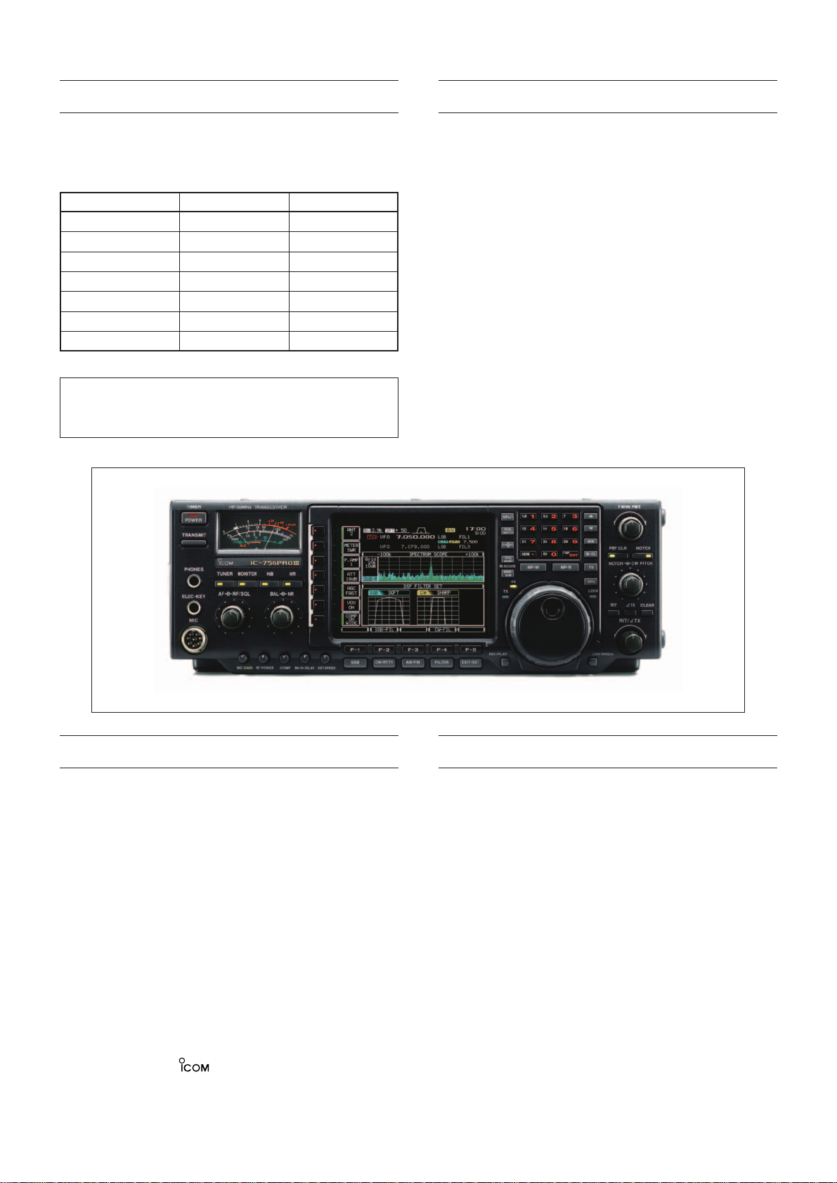
GUIDE FOR CD
1) COMPOSITION
IC_756PRO3
A3format.pdf
756PRO3.pdf
FYC
A4format.pdf
Instruction.pdf
Unitparts.pdf
ar505eng.exe
Installer
W_README.txt
2) DESCRIPTION
756PRO3.pdf
756PRO3.pdf is a service manual for IC-756PROIII and including all service information in this CD. This file is
mainly used for viewing on the computer display and checking page order to make printed service manual. Or
when you want to find a component, you can find very fast using “FIND” function (except Board layout).
A3format.pdf
A3format.pdf consists of A3 format pages (Board layout, Mechanical parts and disassembly, and etc.) in
756PRO3.pdf. This file is used for printing out A3 format pages.
A4format.pdf
A4format.pdf consists of A4 format pages (Circuit description, Adjustment procedures, Parts list, and etc.) in
756PRO3.pdf. This file is used for printing out A4 format pages.
Instruction.pdf
Instruction.pdf is a instruction manual for IC-756PROIII. This file is exactly same as supplying instruction
manual withproduct and consists of all A4 format pages. If you have A4 format printer, you can print out and
make brand new instruction manual any time you want. Also this fi le is very helpful when you want to change
or set product conditionfor adjustment or else.
Unitparts.pdf
Unitparts.pdf is assemble unit information for IC-756PROIII. This information for authorized dis-tributor/dealer
only. Because we (ICOM INC.) don’t sell assemble unit to general.
ar505eng.exe
ar505eng.exe is an installation program of Adobe Acrobat® Reader 5.0 (English version) for Microsoft®
Windows® 95/98/Me/NT/2000/XP users.
1
Page 2

W_README.txt
W_README.txt is a readme text about this service manual for Windows® user that not installed Acrobat®
Reader yet.
=========================================================================================
Icom, Icom Inc. and Icom logo are registered trademarks of Icom Incorporated (Japan) in the United states, the
United Kingdom, Germany, France, Spain, Russia and/or other countries.
Acrobat Reader Copyright © 1987-2002 Adobe Systems Incorporated. All rights reserved.
Adobe, the Adobe logo, Acrobat, and the Acrobat logo are trademarks of Adobe Systems Incorporated.
Microsoft and Windows are registered trademarks of Microsoft Corporation in the U.S.A. and other countries.
Copyright 2004 Icom Inc.
=========================================================================================
2
Page 3

HF/50MHz ALL MODE TRANSCEIVER
SERVICE
MANUAL
Page 4
U.S.A.
Europe
France
United Kingdom
Italy
Korea
Spain
#32
#33
#34
#35
#38
#39
#40
USA
EUR
FRA
UK
ITA
KOR
ESP
INTRODUCTION
This service manual describes the latest service information
for the IC-756PROIII HF/50MHz ALL MODE TRANSCEIVER.
DANGER
NEVER connect the transceiver to an AC outlet or to a DC
power supply that uses more than 16 V. This will ruin the
transceiver.
DO NOT expose the transceiver to rain, snow or any liquids.
DO NOTre v erse the polarities of the power supply when con-
necting the transceiver.
DO NOT apply an RF signal of more than 20 dBm (100 mW)
to the antenna connector. This could damage the transceiver’s front end.
ORDERING PARTS
Be sure to include the following four points when ordering
replacement parts:
1. 10-digit order numbers
2. Component part number and name
3. Equipment model name and unit name
4. Quantity required
<SAMPLE ORDER>
1110000960 S.IC NJM4558M IC-756PROIII MAIN-A UNIT 5 pieces
8810005770 Screw BiH M3
×8 ZK IC-756PROIII Top cover 10 pieces
Addresses are provided on the inside back cover for your
convenience.
REPAIR NOTES
1. Make sure a problem is internal before disassembling the
transceiver.
2.
DO NOT open the transceiver until the transceiver is
disconnected from its power source.
3.
DO NOT force any of the variable components. Turn
them slowly and smoothly.
4.
DO NOT shor t any circuits or electronic parts. An insulated tuning tool
MUST be used for all adjustments.
5.
DO NOT keep power ON for a long time when the transceiver is defective.
6.
DO NOT transmit power into a signal generator or a
sweep generator.
7.
ALWAYS connect a 50 dB to 60 dB attenuator between
the transceiver and a deviation meter or spectrum analyzer when using such test equipment.
8.
READ the instructions of test equipment thoroughly
before connecting equipment to the transceiver.
To upgrade quality, any electrical or mechanical parts and
internal circuits are subject to change without notice or
obligation.
Icom, Icom Inc. and are registered trademarks of Icom Incor porated (Japan) in the United States, the United Kingdom,
Germany, France, Spain, Russia and/or other countries.
VER.NO. SYMBOL VERSION
Page 5

TABLE OF CONTENTS
SECTION 1 SPECIFICATIONS
SECTION 2 INSIDE VIEWS
SECTION 3 CIRCUIT DESCRIPTION
SECTION 4 ADJUSTMENT PROCEDURES
SECTION 5 PARTS LIST
SECTION 6 MECHANICAL PARTS AND DISASSEMBLY
SECTION 7 SEMI-CONDUCTOR INFORMATION
SECTION 8 BOARD LAYOUTS
8 - 1 DISPLAY BOARD . . . . . . . . . . . . . . . . . . . . . . . . . . . . . . . . . . . . . . . . . . . . . . . . . . . . . . . . . . . . . . . .8 - 1
8 - 2 MODE BOARD . . . . . . . . . . . . . . . . . . . . . . . . . . . . . . . . . . . . . . . . . . . . . . . . . . . . . . . . . . . . . . . . . .8 - 3
8 - 3 PHONE BOARD . . . . . . . . . . . . . . . . . . . . . . . . . . . . . . . . . . . . . . . . . . . . . . . . . . . . . . . . . . . . . . . . .8 - 3
8 - 4 KEY BOARD . . . . . . . . . . . . . . . . . . . . . . . . . . . . . . . . . . . . . . . . . . . . . . . . . . . . . . . . . . . . . . . . . . .8 - 3
8 - 5 TEN-KEY BOARD . . . . . . . . . . . . . . . . . . . . . . . . . . . . . . . . . . . . . . . . . . . . . . . . . . . . . . . . . . . . . . .8 - 3
8 - 6 PBT BOARD . . . . . . . . . . . . . . . . . . . . . . . . . . . . . . . . . . . . . . . . . . . . . . . . . . . . . . . . . . . . . . . . . . . .8 - 5
8 - 7 RIT BOARD . . . . . . . . . . . . . . . . . . . . . . . . . . . . . . . . . . . . . . . . . . . . . . . . . . . . . . . . . . . . . . . . . . . .8 - 5
8 - 8 MIC BOARD . . . . . . . . . . . . . . . . . . . . . . . . . . . . . . . . . . . . . . . . . . . . . . . . . . . . . . . . . . . . . . . . . . . .8 - 5
8 - 9 MEMORY BOARD . . . . . . . . . . . . . . . . . . . . . . . . . . . . . . . . . . . . . . . . . . . . . . . . . . . . . . . . . . . . . . .8 - 5
8 - 10 MAIN-A UNIT . . . . . . . . . . . . . . . . . . . . . . . . . . . . . . . . . . . . . . . . . . . . . . . . . . . . . . . . . . . . . . . . . . .8 - 7
8 - 11 DSP-A BOARD . . . . . . . . . . . . . . . . . . . . . . . . . . . . . . . . . . . . . . . . . . . . . . . . . . . . . . . . . . . . . . . . . .8 - 9
8 - 12 RF-B UNIT . . . . . . . . . . . . . . . . . . . . . . . . . . . . . . . . . . . . . . . . . . . . . . . . . . . . . . . . . . . . . . . . . . . .8 - 11
8 - 13 BPF-A BOARD . . . . . . . . . . . . . . . . . . . . . . . . . . . . . . . . . . . . . . . . . . . . . . . . . . . . . . . . . . . . . . . . .8 - 13
8 - 14 PREAMP BOARD . . . . . . . . . . . . . . . . . . . . . . . . . . . . . . . . . . . . . . . . . . . . . . . . . . . . . . . . . . . . . . .8 - 13
8 - 15 PLL UNIT . . . . . . . . . . . . . . . . . . . . . . . . . . . . . . . . . . . . . . . . . . . . . . . . . . . . . . . . . . . . . . . . . . . . .8 - 15
8 - 16 PA UNIT . . . . . . . . . . . . . . . . . . . . . . . . . . . . . . . . . . . . . . . . . . . . . . . . . . . . . . . . . . . . . . . . . . . . . .8 - 17
8 - 17 FILTER-A UNIT . . . . . . . . . . . . . . . . . . . . . . . . . . . . . . . . . . . . . . . . . . . . . . . . . . . . . . . . . . . . . . . . .8 - 19
8 - 18 CTRL-A UNIT . . . . . . . . . . . . . . . . . . . . . . . . . . . . . . . . . . . . . . . . . . . . . . . . . . . . . . . . . . . . . . . . . .8 - 21
8 - 19 TUNER-A BOARD . . . . . . . . . . . . . . . . . . . . . . . . . . . . . . . . . . . . . . . . . . . . . . . . . . . . . . . . . . . . . .8- 23
SECTION 9 BLOCK DIAGRAM
SECTION 10 VOLTAGE DIAGRAMS
10 - 1 FRONT UNIT . . . . . . . . . . . . . . . . . . . . . . . . . . . . . . . . . . . . . . . . . . . . . . . . . . . . . . . . . . . . . . . . . . 10 - 1
10 - 2 DSP-A BOARD . . . . . . . . . . . . . . . . . . . . . . . . . . . . . . . . . . . . . . . . . . . . . . . . . . . . . . . . . . . . . . . . 10 - 3
10 - 3 TUNER-A, MEMORY BOARDS AND CTRL-A UNIT . . . . . . . . . . . . . . . . . . . . . . . . . . . . . . . . . . . . . 10 - 5
10 - 4 MAIN-A UNIT . . . . . . . . . . . . . . . . . . . . . . . . . . . . . . . . . . . . . . . . . . . . . . . . . . . . . . . . . . . . . . . . . 10 - 7
10 - 5 PLL UNIT . . . . . . . . . . . . . . . . . . . . . . . . . . . . . . . . . . . . . . . . . . . . . . . . . . . . . . . . . . . . . . . . . . . 10 - 12
10 - 6 PA AND FILTER-A UNITS . . . . . . . . . . . . . . . . . . . . . . . . . . . . . . . . . . . . . . . . . . . . . . . . . . . . . . . 10 - 15
10 - 7 BPF-A, PREAMP BOARDS AND RF-B UNIT . . . . . . . . . . . . . . . . . . . . . . . . . . . . . . . . . . . . . . . . . 10 - 17
Page 6

SECTION 1 SPECIFICATIONS
■ GENERAL
• Frequency coverage:
Receive 0.030–60.000 MHz*
Transmit 1.800–1.999 MHz*2 3.500–3.999 MHz*
5.3305, 5.3465, 5.3665, 5.3715, 5.4035 MHz*
7.000–7.300 MHz*2 10.100–10.150 MHz*
14.000–14.350 MHz*2 18.068–18.168 MHz*
21.000–21.450 MHz*2 24.890–24.990 MHz*
28.000–29.700 MHz*2 50.000–54.000 MHz*
*1 Some frequency bands are not guaranteed.
2
Depending on version.
*
3
*
[USA] only.
• Mode : USB, LSB, CW, RTTY, AM, FM
• Number of memory channels :
101 (99 regular, 2 scan edges)
• Antenna connector : SO-239
phono jack (RCA; 50 Ω)
• Usable temp. range : –10˚C to +50˚C (14˚F to 122˚F)
• Frequency stability : Less than ±0.5 ppm from 1 min. after
power ON.
• Freq. resolution : 1 Hz
• Power supply
requirement:
13.8 V DC ±15%
• Current drain :
Transmit max. power 23 A
Receive stand-by 3.0 A (typical)
max. audio 3.3 A (typical)
• Dimensions : 340(W)×111(H)×285(D) mm
3
(proj. not included) ; 3
⁄8(W)×43⁄8(H)×117⁄32(D) in
• Weight (approx.) : 9.6 kg (21 lb 3 oz)
• ACC 1 connector : 8-pin DIN connector
• ACC 2 connector : 7-pin DIN connector
• CI-V connector : 2-conductor 3.5(d) mm (
• Display : 5-inch (diagonal) TFT color LCD
,
1
2
*
× 2 (50 Ω)
(–10˚C to +50˚C; 14˚F to 122˚F)
(negative ground)
1
⁄8")
2
3
2
2
2
2
■ TRANSMITTER
• Output power :
SSB/CW/RTTY/FM 5–100 W
AM 5–40 W
• Modulation system :
SSB PSN modulation
AM Low power modulation
FM Phase modulation
• Spurious emission : Less than –50 dB (HF bands)
Less than –60 dB (50 MHz band)
• Carrier suppression : More than 40 dB
• Unwanted sideband suppression:
More than 55 dB
• TX variable range : ±9.999 kHz
• Mic. connector : 8-pin connector (600 Ω)
1
• ELE-KEY connector: 3-conductor 6.35(d) mm (
• KEY connector : 3-conductor 6.35(d) mm (
• SEND connector : Phono jack (RCA)
• ALC connector : Phono jack (RCA)
⁄4")
1
⁄4")
■ RECEIVER
• Receive system : Triple-conversion
superheterodyne system
• Intermediate frequencies:
1st IF 64.455 MHz
2nd IF 455 kHz
3rd IF 36 kHz
• Sensitivity :
SSB, CW, RTTY (at 2.4 kHz bandwidth)
1
1.8–29.99 MHz*
50.0–54.0 MHz*
0.16 µV (10 dB S/N)
2
0.13 µV (10 dB S/N)
AM (at 6.0 kHz bandwidth)
0.5–1.799 MHz 13 µV (10 dB S/N)
1
1.8–29.99 MHz*
50.0–54.0 MHz*
FM (at 15 kHz bandwidth)
28.0–29.99 MHz*
50.0–54.0 MHz*
*1 Pre-amp 1 ON *2 Pre-amp 2 ON
2.0 µV (10 dB S/N)
2
1.0 µV (10 dB S/N)
1
0.5 µV (12 dB SINAD)
2
0.32 µV (12 dB SINAD)
• Squelch sensitivity : (Pre-amp OFF)
SSB/CW/RTTY Less than 5.6 µV
FM Less than 1.0 µV
• Selectivity :
SSB/RTTY (at 2.4 kHz bandwidth)
More than 2.4 kHz/–6 dB
Less than 3.6 kHz/–60 dB
CW (at 500 Hz bandwidth)
More than 500 Hz/–6 dB
Less than 700 Hz/–60 dB
AM (at 6 kHz bandwidth)
More than 6.0 kHz/–6 dB
Less than 15.0 kHz/–60 dB
FM (at 15 kHz bandwidth)
More than 12 kHz/–6 dB
Less than 20 kHz/–60 dB
• Spurious and image rejection ratio:
More than 70 dB
(except IF through in 50 MHz band)
• RIT variable range : ±9.999 kHz
• Audio output power : More than 2.0 W at 10% distortion
(at 13.8 V DC) with an 8 Ω load
• PHONES connector: 3-conductor 6.35(d) mm (
• EXT SP connector : 2-conductor 3.5(d) mm (
1
1
⁄8") 8
⁄4")
Ω
■ ANTENNA TUNER
• Matching impedance range:
HF bands 16.7 to 150 Ω unbalanced*
50 MHz band 20 to 125 Ω unbalanced*
*1 Less than VSWR 3:1 *2 Less than VSWR 2.5:1
• Minimum operating input power:
8 W
• Tuning accuracy : VSWR 1.5:1 or less
• Insertion loss : Less than 1.0 dB
(after tuning)
1
2
All stated specifications are subject to change without notice or obligation.
1 - 1
Page 7
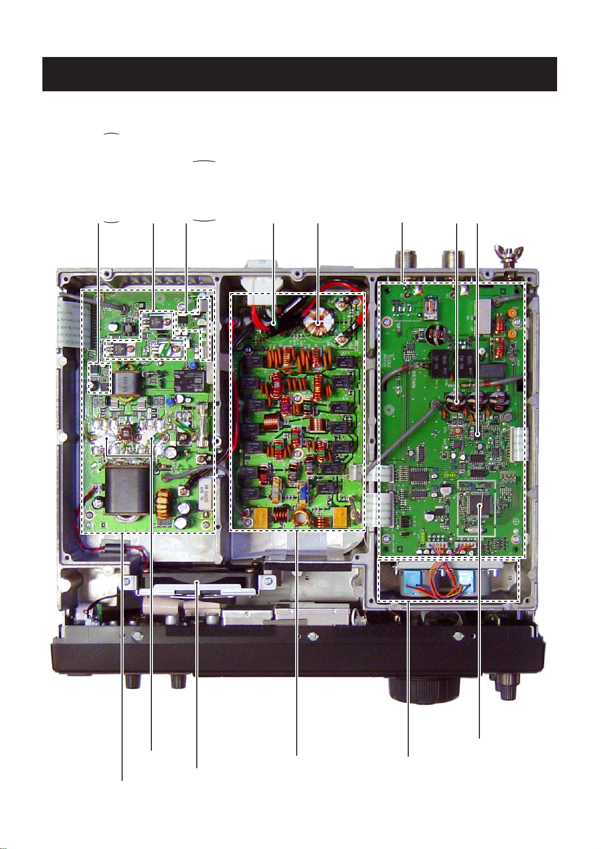
SECTION 2 INSIDE VIEWS
2 - 1
• TOP VIEW
Fan control circuit
PA unit
Fan
FILTER-A unit
TUNER-A unit
Antenna tuner CPU
(IC5: M38022M2-138FP)
Drive amplifier
Voltage regulator
Common filter
(L501: LR-386)
Common filter
(L502: LR-386)
CTRL-A unit
Current transformer
(L1: LR-364)
C-MOS IC
(IC14: TC74AC04F)
Fan control circuit
Q10, Q11: 2SC4081×2
Q12, Q13: 2SB1201×2
PA unit
Cooling fan
FILTER-A unit
TUNER-A unit
Antenna tuner CPU
(IC5: M38022M2-138FP)
Drive amplifier circuit
(Q2, Q3: 2SC1972×2)
Voltage regulator
IC1: TA7805F
IC2: TA7805S
IC3: TA78T08C
Common filter
(L501: LR-386)
Common filter
(L502: LR-386)
CTRL-A unit
Current transformer
(L1: LR-364)
C-MOS IC
(IC14: TC74AC04F)
Power amplifier
(Q4, Q5: 2SC5125×2)
Power amplifiers
(Q4, Q5: 2SC5125×2)
Page 8
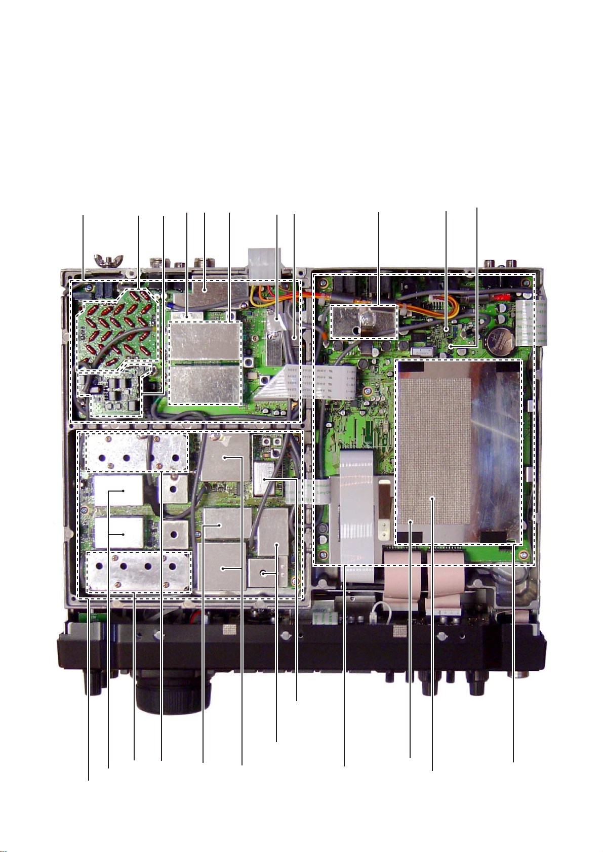
2 - 2
• BOTT OM VIEW
Reference frequency oscillator
(X52: CR-338 32.00056MHz)
RF-B unit
BPF-A board
PLL unit
1LO PLL IC
(IC381, IC681: LMX2306TM)
VCO-B circuit
VCO-A circuit
S2LO PLL IC
(IC901: LC7153M)
1LO DDS IC
(IC101, IC401: SC-1246A)
3LO/S3LO DDS IC
(IC701, IC801: SC-1287)
MAIN-A unit
Noise blanker circuit
LCD contorller
(IC3551: S1D13504F00A000)
MAIN CPU
(IC3501: HD64F2375F20)
TX 3rd mixer
(IC221: NJM1496V)
RX 3rd mixer
(IC151: TC4W53FU)
DSP-A board
PREAMP board
TX 1st mixer
(D1451: HSB88WS)
FM IF IC
(IC2001: TA3116FN)
RX 1st mixer circuit
RX 2nd mixer
(D1752: HSB88WS)
TX 2nd mixer
(D1852: HSB88WS)
Reference frequency oscillator
(X52: CR-338. 32.00056MHz)
RF-B unit
BPF-A board
PLL unit
1LO PLL IC
(IC381, IC681: LMX2306TM)
VCO-B circuit
VCO-A circuit
S2LO PLL IC
(IC901: LC7153M)
1LO DDS IC
(IC101, IC401: SC-1246A)
3LO/S3LO DDS IC
(IC701, IC801: SC-1287)
MAIN-A unit
Noise blanker circuit
LCD contorller
(IC3551: S1D13504F00A000)
MAIN CPU
(IC3501: HD64F2375F20)
TX 3rd mixer
(IC221: NJM1496V)
RX 3rd mixer
(IC151: TC4W53FU)
DSP-A board
PREAMP board
TX 1st mixer
(D1451: HSB88WS)
FM IF IC
(IC2001: TA3116FN)
RX 1st mixer circuit
RX 2nd mixer
(D1752: HSB88WS)
TX 2nd mixer
(D1852: HSB88WS)
Page 9
SECTION 3 CIRCUIT DESCRIPTION
•
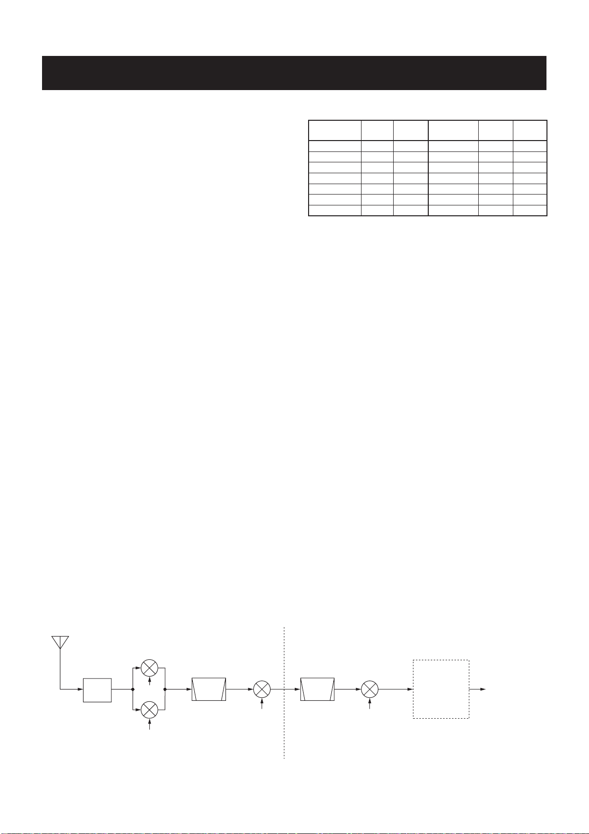
3-1 RECEIVER CIRCUIT
3-1-1 RF SWITCHING CIRCUIT
(CTRL-A AND RF-B UNITS)
The RF switching circuit leads receive signals to bandpass
fi lters from an antenna connector while receiving. However,
the circuit leads the signal from the RF power amplifier to
the antenna connector while transmitting.
RF signals from [ANT 1] or [ANT 2] pass through the antenna selector (RL3), transmit/receive switching relays (RL1,
RL2, RL4), and low-pass fi lter (L27, L28, C63–C66, C105),
and are then applied to the RF-B unit via J101 (RF-B unit).
The signals from the CTRL-A unit either bypass or pass
through the 6 dB (RF-B unit, R102, R106, R111, RL102)
and/or 12 dB (RF-B unit, R112, R113, R114, RL103)
attenuators via the antenna selector (RL101). By selecting
the attenuators, 0 (bypass), 6, 12 and 18 dB attenuations
are obtained. The signals are then applied to the RF fi lters.
When the [RX ANT] is selected, the RF signals are passed
through the low-pass filter (RF-B unit, L101, L102, C101
–C105), then applied to the antenna selector (RF-B unit,
RL101).
3-1-2 RF BANDPASS FILTER CIRCUIT
(RF-B UNIT AND BPF-A BOARD)
RF bandpass fi lters pass only the desired band signals and
suppress any undesired band signals. The RF circuit has 11
bandpass fi lters and 1 low-pass fi lter.
• Used RF fi lter
Band
0.03–1.6 MHz B0 D801 11–15 MHz B7 D551
1.6–2 MHz B1 *D3201 15–22 MHz B8 D602
2–3 MHz B2 *D3301 22–30 MHz B9 D651
3–4 MHz B3 *D3401 30–50 MHz B10W D701
4–6 MHz B4 *D3501 50–54 MHz B10 D751
6–8 MHz B5 *D3601 54–60 MHz B10W D701
8–11 MHz B6 D501
*: On the BPF-A board
Control
signal
Input
diode
Band
Control
signal
Input
diode
3-1-3 PRE-AMPLIFIER CIRCUITS (PRIAMP BOARD)
The IC-756PROIII has 2 gain levels of pre-amplifi er circuits.
One has 10 dB gain for the 1.8–21 MHz bands and the other
one has 16 dB gain for the upper 24 MHz bands.
When the [P.AMP] switch is set to [P.AMP 1] or [P.AMP
2], the signals are applied to the pre-amplifier 1 (Q4201,
Q4202) or pre-amplifi er 2 (Q4302) circuit, respectively. Preamplifi ed or bypassed signals are applied to the RF amplifi er
circuits (RF-B unit; Q1001, Q1002 or Q1201, Q1202).
3-1-4 RF AMPLIFIER AND 1ST MIXER CIRCUITS
(RF-B UNIT)
The 1st mixer circuit mixes the receive signals with the 1st
LO signal to convert the receive signal frequencies into a
64.455 MHz 1st IF signal. The IC-756PROIII has two 1st
mixer circuits for the dualwatch function.
(1) 0.03–1.6 MHz (RF-B UNIT)
The signals pass through the low-pass filter (L801–L802,
C802, C805–C807), attenuator (R801–R803), and are then
applied to the RF amplifi ers (Q1001, Q1002).
The signals from the pre-amplifier circuit, or signals which
bypass the pre-amplifi ers, are divided at L902, L903. Each
signal is applied to a 60 MHz cut-off low-pass fi lter, RF amplifi er (Q1001, Q1002 for sub readout or Q1201, Q1202 for
main readout) and then to a 1st mixer (Q1003–Q1006 sub
(2) 1.6–60 MHz (RF-B UNIT AND BPF-A BOARD)
The signals pass through the band switch (D104) and high-
readout or Q1203–Q1206 for main readout) to convert the
frequency into the 64.455 MHz 1st IF signal.
pass filter (L251–L253, C251, C252, C271–C274) to suppress excessively strong signals below 1.6 MHz. The fi ltered
signals are applied to one of 11 bandpass fi lters on the table
at right above, and then applied to or bypassed the preamplifi er circuit.
Each 1st LO signal (64.4850–124.4550 MHz) from the PLL
unit via J1101 or J1301. The LO signals are amplifi ed at the
LO amplifi er (Q1101; sub or Q1301; main), fi ltered by a lowpass fi lter, and then applied to each 1st mixer.
Receiver construction
1st mixer B
Q1003–Q1006
FI1701
LPF or
BPF
0.03–60.0 MHz
1st LO B
1st mixer A
Q1203–Q1206
1st LO A
Crystal
filter
64.455 MHz
2nd mixer
D1752
2nd LO
64.0 MHz
RF-B UNIT MAIN-A UNIT
FI111
Ceramic
filter
455 kHz
3rd mixer
IC151
3rd LO
491 kHz
36 kHz
DSP-A
board
to squelch gate
(IC301)
3 - 1
Page 10

3-1-5 1ST IF CIRCUIT (RF-B UNIT)
The 1st IF circuit filters and amplifies the 1st IF signal. The
1st IF signal combined at L1018 and is then applied to a
MCF (Monolithic Crystal Filter; FI1701) to suppress out-ofband signals.
The 1st IF signal level is adjusted at the PIN attenuators
(D1001, D1003, D1004; sub or D1201, D1203, D1204 for
main) controlled by the [BAL] controller for the dualwatch
function. The signal is applied to the 1st IF amplifier (Q1008;
sub or Q1208; main) and then combined at L1018.
The combined signal is pass through the MCFs (FI1701)
and is then applied to the 1st IF amplifier (Q1751). The
amplified signal is then applied to the 2nd mixer circuit.
Some DC voltage from the noise detector circuit is fed back
to the noise amplifiers (Q271, Q272) via the DC amplifiers
(Q274, Q275). The DC amplifiers function as an AGC circuit to reduce average noise. Therefore, the noise blanker
function shuts off pulse-type noise only.
3-1-8 2ND IF CIRCUIT (MAIN-A UNIT)
The 2nd IF circuit amplifies and filters the 2nd IF signal,
and applies the 2nd IF signal to the 3rd mixer circuit.
The 2nd IF signal from the noise blanker gate (D113,
D114) is amplified at the 2nd IF amplifier (Q141) and
passed through the ceramic filter (FI111). The filtered signal is applied to the 3rd mixer circuit.
3-1-6 2ND MIXER CIRCUIT (RF-B UNIT)
The 2nd mixer circuit mixes the 1st IF signal and 2nd LO
signal (64.00 MHz) for conversion into the 2nd IF signal.
The 1st IF signal from the 1st IF amplifier (Q1751) is converted into a 455 kHz 2nd IF signal at the 2nd mixer circuit
(D1752).
The 2nd IF signal is applied to the noise blanker gate
(MAIN-A unit) via the J1851.
3-1-7 NOISE BLANKER CIRCUIT (MAIN-A UNIT)
The noise blanker circuit detects pulse-type noise, and
turns OFF the signal line when the noise appears.
The 2nd IF signal from the RF-B unit is applied to the noise
blanker gate (D113, D114).
A portion of the 2nd IF signal is amplified at the noise
amplifiers (Q271–Q273, Q279), and is then detected at the
noise detector (D271) to convert the noise components to
DC voltages.
The signal is then applied to the noise blanker switch (Q276,
Q278). At the moment the detected voltage exceeds Q276’
s threshold level, Q278 outputs a blanking signal to close
the noise blanker gate (D113, D114). The PLL unlock signal are also applied to Q278, to control the noise blanker
gate.
3-1-9 3RD MIXER AND 3RD IF CIRCUITS
(MAIN-A UNIT)
The 3rd mixer circuit mixes the 2nd IF signal and the 3rd
LO signal to obtain the 3rd IF (36 kHz) signal.
The 2nd IF signal from the ceramic filter (FI111) is applied
to the 3rd mixer circuit (IC151, pin 1). The 3rd LO signal
from the PLL unit is applied to the 3rd mixer (IC151, pin 5).
The 3rd IF signal is output from pin 6.
The 3rd IF signal is passed through the low-pass filter
(IC201a) and amplified at the 3rd IF amplifier (IC201b). The
amplified signal is then applied to the DSP-A board via
J201 (pin 27) as DRIF signal.
3-1-10 DSP RECEIVER CIRCUIT (DSP-A BOARD)
The DSP (Digital Signal Processor) circuit enables digital
IF filter, digital noise reduction, digital PSN (Phase Shift
Network)/Low Power/Phase demodulation, digital automatic
notch, and etc.
The 36 kHz 3rd IF signal from the 3rd IF amplifier (MAIN-A
unit, IC201b) is amplified at the differential amplifiers
(IC2301a/b) after being passed through the T/R switch
(IC2291), and is then applied to the A/D converter (IC2321).
• DSP receiver circuit
“TXS” signal
3rd IF
signal
36 kHz
MAIN-A unit DSP-A board MAIN-A unit
DRIF
IC2291
5
6
7
T/R switch
“TXS” signal
IC2301b/a IC2321
Differential
1
converter
IC2372x
13
14
12
11
A/D
converter
IC2372y
1
10
IC2051
converter
IC2401
15
“TXS” signal
Level
LPF
IC2001
DSP IC
IC2372z
4
9
5
3
IC2052
Level
converter
IC2473
1
7
4
IC2351
D/A
converter
IC2441a
HPF
IC2471a
Mixer
amplifier
DRAF
3 - 2
AF
signals
Page 11

The converted signal is changed from a 5 V level signal to
a 3.3 V signal in the level converter (IC2051), and is then
applied to the DSP IC (IC2001) for 36 kHz digital IF filter,
demodulation, automatic notch and noise reduction, etc.
The output signal from the DSP IC (IC2001) is changed
from a 3.3 V level signal to a 5 V level signal in the level
converter (IC2502), and is applied to the D/A converter
(IC2351) to convert into the analog audio signals.
The converted audio signals are passed through the active
filter (IC2371a), AF amplifier (IC2371b), analog switches
(IC2372, pins 13, 14 and pins 1, 15) then applied to the
low-pass filter (IC2401, pins 5, 11). The filtered signals are
passed through the analog switches (IC2372, pins 3, 4 and
IC2473, pins 1, 7), high-pass filter (IC2441A) and mixer
amplifier (IC2471A), and then applied to the MAIN-A unit
via J2001 (pin 13) as the DRAF signal.
3-1-11 TWIN PBT CIRCUIT (DSP-A BOARD)
General PBT (Passband Tuning) circuit shifts the center frequency of IF signal to electronically narrow the passband
width. The IC-756PROIII uses the DSP circuit for the digital
PBT function and actually shifts the both lower and higher
passbands of 3rd IF filter within ±1.8 kHz.
The twin PBT circuit in DSP IC (IC2001) controlled by the
[TWIN PBT] controller adjusts the 3rd IF passband width
and rejects interference.
3-1-13 S-METER CIRCUIT (MAIN-A UNIT)
The S-meter circuit indicates the relative received signal
strength while receiving by utilizing the AGC voltage which
changes depending on the received signal strength.
A portion of the AGC bias voltage from the DSP-A board
is applied to the differential amplifier (IC101a, pin 2) where
the difference between the AGC and reference voltage is
detected.
The detected voltage is passed through the analog switch
(IC3631, pins 12, 14) as the SML signal and applied to the
main CPU (IC3501, pin 108) to activate the S/RF meter via
the sub CPU (DISPLAY board, IC401).
3-1-14 SQUELCH CIRCUIT (MAIN-A UNIT)
The squelch circuit mutes audio output when the S-meter
signal is lower than the [RF/SQL] setting level.
The S-meter signal is applied to the main CPU (IC3501, pin
108) and is compared with the threshold level set by the
[RF/SQL] control. The [RF/SQL] setting signal is applied to
the main CPU via the sub CPU (DISPLAY board; IC401,
pin 91). The main CPU analyzes the compared signal and
outputs control signal to the squelch gate (IC301, pin 5)
via the interface IC (IC3653, pin 19) to open or close the
squelch as the SQLS signal.
3-1-12 AGC CIRCUIT (DSP-A BOARD)
The AGC (Automatic Gain Control) circuit reduces IF amplifier gain and attenuates IF signal to keep the audio output
at a constant level.
The receiver gain is determined by the voltage on the
AGC line (IC2461, pin 4). The D/A converter (IC2461) for
AGC supplies control voltage to the AGC line and sets the
receiver gain with the [RF/SQL] control.
The 3rd IF signal from the level converter (IC2051) is
detected at the AGC detector section in DSP IC (IC2001),
and is applied to the D/A converter for AGC via the level
converter (IC2052). The AGC voltage is amplified at the
buffer amplifier (IC2471b), and is then applied to the
MAIN-A unit via J2001 (pin 16) to control the AGC line.
When receiving strong signals, the AGC voltage decreases
via the buffer amplifier (IC2471b). As the AGC voltage is
used for the bias voltage of the IF amplifier (RF-B unit;
Q1751), and IF amplifier gain is decreased.
• AF amplifier circuit
DRAF
IC301 IC311
7
6
5
MAIN-A unitDSP-A board
“SQLS” signal
2
1
AMP VCA
“AFGV” signal
9
3-1-15 AF AMPLIFIER CIRCUIT (MAIN-A UNIT)
The AF amplifier amplifies the audio signals to a suitable
driving level for the speaker.
The AF signals (DRAF) from the DSP-A board are passed
through the squelch gate (IC301, pins 1, 7) and amplified
at the AF amplifier section of IC311 (pins 2, 4), and volume
is controlled by the AFGV signal at the VCA section (pins 7
–9). The volume controlled AF signals are passed through
the AF mute gate (IC331, pins 1, 7), then applied to the AF
power amplifier (IC332, pins 1, 4).
The amplified audio signals are passed through the SP
mute switch (RL351) and [EXT SP] jack then applied to the
internal speaker when no plug is connected to the jack.
The AF mute gate is controlled by the [AF] control via the
sub and main CPUs.
When headphones are connected, the SP mute signal from
the main CPU (IC3501, pin 56) is applied to the SP mute
switch (RL351) via the BUS driver (IC3654, pins 8, 13) as
the SPS signal.
IC331
1
Mute switchSquelch gate
“AFMS” signal
2
6
7
IC332
AF
power
amp.
“SPS” signal
RL351
[PHONES]
[EXT SP]
Int. speaker
3 - 3
Page 12
3-2 TRANSMITTER CIRCUITS
3-2-1 MICROPHONE AMPLIFIER CIRCUIT
(MAIN-A UNIT)
The microphone amplifier circuit amplifies microphone
audio signals to a level needed for the DSP circuit.
Audio signals from the [MIC] connector (MIC board; J1,
pin 1) are amplified at the audio amplifier section in IC451
(pins 21, 22) via the analog switch (IC3002, pins 12, 14),
then applied to the buffer amplifier section (IC451, pin 5)
and VCA section. The gain controlled signals are output
from (IC451, pin 9) and passed through the analog switch
(IC3005, pins 12, 14) and then applied to the DSP circuit
via J201 (pin 15) as the DTAF signal.
The VCA section in IC451 (pin 9) controls microphone
input gain according to the [MIC GAIN] control level using
the MIGV signal coming from the main CPU via the I/O
expander (IC3751, pin 4).
(1) When SSB mode
The audio signals from the analog switch (IC2201, pin 5)
are amplified at the limiter amplifier (IC2281b) and applied
to the low-pass filter (IC2281c/d) to limit the transmit
passband width.
The filtered signals are then applied to the differential
amplifiers (IC2301a/b) via the analog switch (IC2201, pins
12, 14) and T/R switch (IC2291, pins 1, 7).
(2) When FM/AM modes
The audio signals from the analog switch (IC2201, pin 3)
are applied to the modulation adjustment pots (R2227:
FM mode, R2229: AM mode) via the limiter amplifier, preemphasis circuit (only FM mode) and splatter filter consist
of IC2211. The level adjusted signals are applied to the differential amplifiers (IC2301a/b) after being passed through
the analog switch (IC2201, pins 1, 2, 13–15) and T/R
switch (IC2291 pins 1, 7). The pre-emphasis circuit is cancelled by Q2201, Q2202, Q2211 on AM mode.
3-2-2 VOX CIRCUIT (MAIN-A UNIT)
The VOX (Voice-Operated Transmission) circuit sets transmitting conditions according to voice input.
A portion of the audio signals from the VCA section (IC451,
pin 9) is applied to the AF amplifier (IC3004b, pins 6, 7),
and then applied to the main CPU (IC3501, pin 106) after
passing through the analog switch (IC362, pins 1, 6) as the
VOXL signal.
The VOGV signal is applied to the VCA section in IC3003
(pin 8) from the main CPU via the I/O expander (IC3751,
pin 9) to adjust VOX actionable sensitivity. This is controlled
by the VOX gain set in the VOX SET mode.
3-2-3 DSP TRANSMITTER CIRCUIT
(DSP-A BOARD)
The microphone audio signals from the MAIN-A unit via the
DTAF line are applied to the analog switch (IC2201, pin 4)
and output from pin 3 or 5 to the each modulation circuits.
• DSP Transmitter circuit
The amplified signals at the differential amplifiers (IC2301a/
b) are applied to the A/D converter (IC2321 pins 4, 5). The
converted signals are changed from 5 V level signals to 3.3
V level signals in the level converter (IC2051).
The converted signals are applied to the DSP IC (IC2001)
and modulated at the DSP IC to produce the 36 kHz transmitter IF signal. The modulated IF signal from the DSP IC
is changed from a 3.3 V signal to a 5 V signal in the level
converter (IC2052), and is applied to the D/A converter
(IC2351) to convert into the analog IF signal.
The converted IF signal is passed through the active filter (IC2371a), buffer amplifier (IC2371b), analog switch
(IC2372, pins 12, 14) then applied to the low-pass filter
(IC2381c/d). The filtered signal is applied to the MAIN-A
unit via J2001 (pin 29) as the DTIF signal.
When SSB or RTTY mode, a portion of the filtered signal
from the low-pass filter (IC2381c/d) is amplified at the IF
and buffer amplifiers (IC2381a/b) and is applied to the
transmit monitor circuit for the monitor function.
IC2201z
AF
DTAF
signal
MAIN-A unit DSP-A board
9
4
Mode switch
SSB
5
mode
3
FM/AM
mode
IC2321
A/D
converter
“MODS” signal
Limitter
IC2211a
Limitter
IC2051
Level
converter
IC2281c/dIC2281b
LPF
IC2211b
LPF
IC2001
DSP IC
IC2201x
12
13
Mode switch
IC2052
Level
converter
3 - 4
11
14
converter
IC2291
5
6
7
T/R switch
IC2351
D/A
“TXS” signal
“TXS” signal
IC2301a/b
Differential
1
converter
IC2372x
14
11
13
12
IC2381d/c
LPF
DTIF
MAIN-A unit
36 kHz IF
Page 13

3-2-4 SPEECH COMPRESSOR CIRCUIT
(DSP-A BOARD)
The speech compressor compresses the transmitter audio
input signals to increase the average output level (average
talk power).
When the speech compressor function is ON, the level
shifted signal from the level converter (IC2051) is applied
to the DSP IC (IC2001) and compressed at the DSP IC to
obtain an average audio level.
At the same time, the compressed signals are modulated
at the DSP IC and applied to the level converter (IC2052).
3-2-5 IF AMPLIFIER AND MIXER CIRCUITS
(MAIN-A AND RF-B UNITS)
The modulated 3rd IF signal from the DSP-A board (DTIF:
36 kHz) is applied to the 3rd mixer circuit (MAIN-A unit;
IC221, pin 1). The applied 3rd IF signal is mixed with the
3rd LO signal from the DDS circuit (PLL unit; IC701) to produce a 455 kHz 2nd IF signal.
The 2nd IF signal is output from (MAIN-A; IC221, pin 6)
and amplified at the IF amplifier (MAIN-A unit; Q241). The
amplified signal is passed through the ceramic bandpass
filter (MAIN-A unit; FI131: FM/AM modes, FI133: other
modes) for unwanted signals are suppressed. The filtered
2nd IF signal is amplified at IF amplifier (MAIN-A unit;
Q261) and applied to the 2nd mixer circuit on the RF-B unit
via J101 (MAIN-A unit).
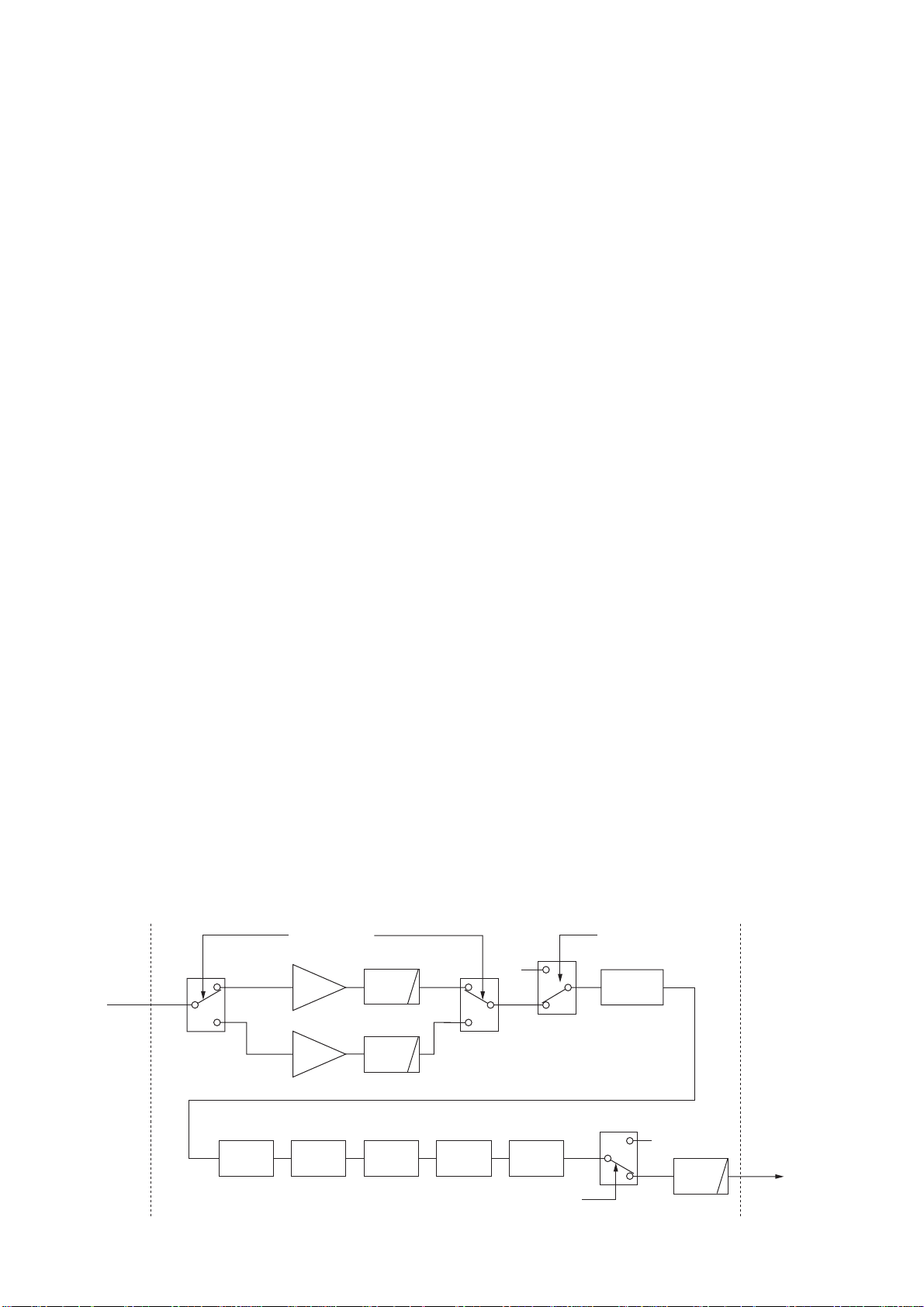
3-2-6 RF CIRCUIT (RF-B AND PA UNITS)
The RF circuit amplifies operating (transmitting) frequency
to obtain 100 W of RF output.
The signal from the 1st IF mixer (RF-B unit; D451) is
passed through the low-pass filter (RF-B unit; L1402,
L1403, C1405–C1409) and amplified at the RF amplifier
(RF-B unit; IC1401). The amplified signal is amplified again
at the wide-band YGR amplifier (RF-B unit, IC201) after
passing through one of 10 bandpass (Refer to page 3-1
for bandpass filters used) and high-pass filters, and is then
applied to the PA unit via J201 (RF-B unit).
The signal applied from the RF-B unit is amplified at the
pre-drive (Q1), drive (Q2, Q3) and power amplifiers (Q4,
Q5) in sequence to obtain a stable 100 W of RF output
power. The amplified signal is applied to one of 8 low-pass
filters in the FILTER-A unit.
3-2-7 LOW-PASS FILTER CIRCUIT (FILTER-A UNIT)
The low-pass filter circuit contains 8 Chebyschev low-pass
filters to suppress the higher harmonic components.
The amplified signal from the PA unit is applied to one of
8 low-pass filters, which is selected by the I/O expander
(CTRL-A unit, IC11) via the buffer amplifier (CTRL-A unit;
IC12).
The filtered signal is then applied to one of 2 antenna connectors via the CTRL-A unit.
The 2nd IF signal is mixed with the 64 MHz 2nd LO signal,
coming from the PLL unit, at the 2nd mixer circuit (RF-B
unit; D1852) to obtain a 64.455 MHz 1st IF signal. The 1st
IF signal is passed through a MCFs (RF-B unit; FI1701)
to cut-off the undesired signals then amplified at the IF
amplifier (RF-B unit; Q1551) via the T/R switch (RF-B unit;
D1551). The amplified 1st IF signal is applied to the 1st IF
mixer circuit (RF-B unit; D1451).
The operating (transmitting) frequency is produced at the
1st IF mixer circuit (RF-B unit; D1451) by mixing the 1st IF
and 1st LO signals. The mixed signal is then applied to the
RF circuit.
• Transmitter construction
IC3005x
14
11
12
DTAF
13
MIC
IC3002
13
12
“MISL” signal
14
11
AMP VCA
IC451
“MOSL” signal
DSP-A
board
3-2-8 ALC CIRCUIT (MAIN-A UNIT)
The ALC (Automatic Level Control) circuit controls the gain
of IF amplifiers in order for the transceiver to output a constant RF power set by the [RF POWER] control even when
the supplied voltage shifts, and etc.
The RF power level is detected at one of the APC detector
circuits (CTRL-A unit; D2) to be converted into DC voltage
and applied to the MAIN-A unit as the FORV signal.
The FORV signal from the CTRL-A unit is applied to the
comparator (IC551b, pins 6, 7). The POCV signal, controlled by the [RF POWER] control via the I/O expander
(IC3751, pin 5), is also applied to the other input (IC551b,
pin 5) for reference. The compared signal is output from
pin 7 and applied to the IF amplifiers in the MAIN-A (Q261)
and RF-B (Q1551) units to control amplifying gain.
FI131
Ceramic
filter
FI133
Ceramic
filter
DTIF
36 kHz IF
IC221
455 kHz
3rd LO
(491 kHz)
FM/AM
modes
other
modes
MAIN-A UNIT
D1852
64.455 kHz
2nd LO
(64.00 MHz)
FI1701
Crystal
filter
3 - 5
D1451
1st LO
(64.485–
124.455 MHz)
LPF
RF-B UNIT
BPFs
PAIN
PA UNIT
Page 14

When the FORV signal exceeds the POCV voltage, ALC
bias voltage from the comparator (IC551b) controls the IF
amplifiers (Q261). This adjusts the output power to a specified level from the [RF POWER] control until the FORV and
POCV voltages are equalized.
The thermistor (R50) detects the temperature of the final
amplifier (Q5), and activates Q11 and Q13 to accelerate
the cooling fan when the detected temperature exceeds
70˚C (158˚F). The cooling fan rotates at high speed at 80˚C
(176˚F) or more.
In AM mode, the comparator operates as an averaging ALC
amplifier. Q502 turns ON and the POCV voltage is shifted
for 40 W AM output power (maximum) through R510.
The ALC bias voltage is also applied to the ALC meter
amplifier (IC551a, pins 1, 2) to obtain an ALC meter signal
(ALCL). The amplified signal is passed through the analog
switch (IC 3631, pins 13, 14) and applied to the main CPU
(IC3501, pin 108) to drive the S/RF meter via the sub CPU
(IC401) on the DISPLAY board.
An external ALC input from the [ALC] jack or [ACC] sockets is applied to the buffer amplifier (Q521). External ALC
operation is identical to that of the internal ALC.
The FORV signal is also applied to the power meter amplifier (IC571a, pins 1, 3). The amplified signal is passed
through the analog switch (IC3631, pins 1, 15) as an FORL
signal and applied to the main CPU (IC3501, pin 109) to
drive the S/RF meter when the power meter is selected.
3-2-9 APC CIRCUIT (MAIN-A UNIT)
The APC (Automatic Power Control) circuit protects the
power amplifiers on the PA unit from high SWR and excessive current.
The reflected wave signal appears and increases when the
connected antenna is mismatched to 50 Ω. The APC detector circuit (CTRL-A unit; D1 and L1) detects the reflected
signal, and applies it to the APC circuit (IC551c, pins 9, 8)
as REFV signal.
When the REFV signal level increases, the APC circuit
decreases the ALC voltage to activate the APC.
The thermistor keeps the cooling fan rotating even while
receiving until the Q5 temperature drops to 60˚C (140˚F) or
below.
3-2-11 MONITOR CIRCUIT
(DSP-A BOARD AND MAIN-A UNIT)
The microphone audio signals can be monitored to check
voice characteristics.
(1) When FM/AM modes (MAIN-A UNIT)
A portion of the microphone audio signals from the VCA
section (IC451; pins 9, 22) are applied to the analog switch
(IC361; pins 1, 7). The selected audio signals are applied to
IC371 (pin 2), and the output signals from pin 9 are applied
to the AF amplifier circuit (IC311, pin 2, 9).
(2) When SSB/RTTY modes
A portion of the transmit IF signal from the low-pass filter
(IC2381c/d) is amplified at the IF (IC2381b) and buffer
(IC2381a) amplifiers, and applied to the digital mixer circuit
(IC2302). The applied signal is mixed with a 36 kHz LO signal from the D/A converter (IC2342) to demodulate into the
AF signals. The demodulated signals are passed through
the buffer amplifier (IC2381a), low-pass filter (IC2441b/
c) and AF amplifier (IC2441d), and then applied to the
MAIN-A unit via J2001 (pin 19) as the DMAF signal.
The DMAF signal from the DSP-A board is amplified at the
ALC amplifier (MAIN-A unit; IC372, pins 1, 13) and applied
to the VCA section of IC371 (MAIN-A unit; pins 7, 9). The
volume controlled AF signals is applied to the AF amplifier
circuit (MAIN-A unit; IC311, pins 2, 9).
(DSP-A BOARD)
For the current APC, the power transistor current is
obtained by detecting the voltages (ICH and ICL) which
appear at both terminals of the current detector (PA unit;
R28). The detected voltages are applied to the differential
amplifier (IC551d, pins 12–14). When the current of transistors is increased, the amplifier controls the ALC line to prevent excessive current flow.
A portion of the REFV signal is applied to the SWR meter
amplifier (IC571b, pins 5, 7). The amplified signal is passed
through the analog switch (IC3631, pins 3, 4) as an REFL
signal and applied to the main CPU (IC3501, pin 110) to
drive the S/RF meter when the SWR meter is selected.
3-2-10 TEMPERATURE PROTECTION CIRCUIT
(PA UNIT)
The cooling fan (CHASSIS; MF1) is activated while transmitting or when the temperature of the power amplifier
exceeds the preset value. The temperature protection circuit consists of Q10–Q13 and R50.
While transmitting, Q10 and Q12 are turned ON, and provide a voltage to the cooling fan to rotate at medium speed.
3-3 PLL CIRCUITS
3-3-1 GENERAL
The PLL unit generates a pair of 1st LO frequencies (64.485
–124.455 MHz) for dualwatch and spectrum scope functions; a 2nd LO frequency (64 MHz), 3rd LO frequency
(491 kHz) and sweep LO frequency for the spectrum scope
function.
The 1st LO PLLs adopt a mixer-less dual loop PLL system and has 4 VCO circuits. The LOs, except the 2nd, use
DDSs while the 2nd LO uses the fixed frequency of the
crystal oscillator.
3-3-2 1ST LO PLL CIRCUIT
The 1st LO PLLs contain a main and reference loop as a
dual loop system. Both PLLs have equivalent circuits— this
manual describes only the 1st LO PLL A circuit.
The reference loop generates a 10.747 to 10.865 MHz frequency using a DDS circuit, and the main loop generates a
64.485 to 124.455 MHz frequency using the reference loop
frequency.
3 - 6
Page 15
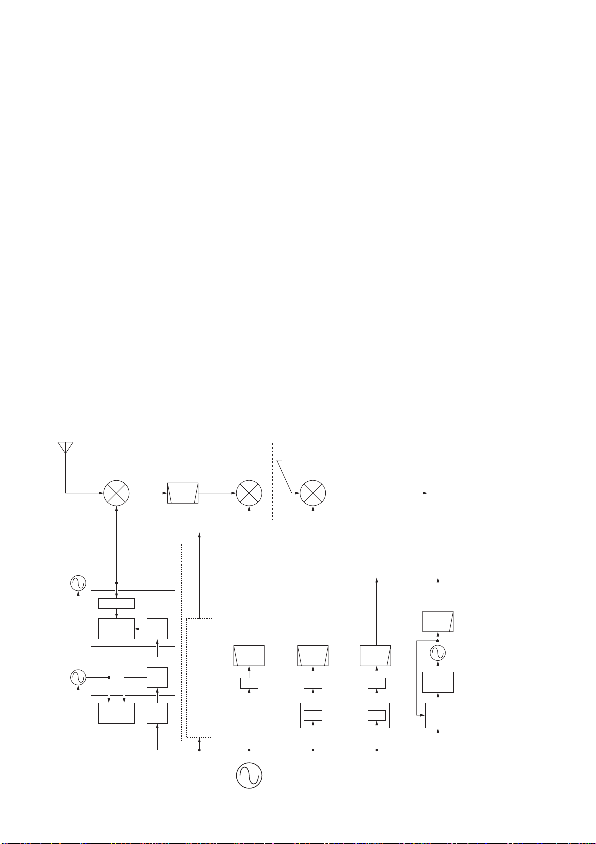
(1) REFERENCE LOOP PLL
• PLL CIRCUIT
64.485–
124.455 MHz
0.03–
60.0 MHz
455 kHz
36 kHz
10.747–
10.865 MHz
64.485–
124.455 MHz
64.0 MHz
77.8 MHz
ANT
1st mixer A
Q1203–Q1206
491 kHz
to scope circuit
(RF-B unit, D2101)
to scope circuit
(RF-B unit, IC2001)
IC801IC701
IC101
IC381
IC901
Q71
Q81
Q902
S2LOS3LO
3LO
X2
2LO
1LOB
1LOA
77.8 MHz
RF-B unit
PLL unit
MAIN-A unit
Q201
Q221
Q251
Q271
Q151
1st LO PLL A
circuit
Phase
detector
1/N divider
1/22
Phase
detector
12 bit
D/A
Main loop PLL
Ref. loop PLL
DDS
1st mixer B
1st LO
PLL B
circuit
DDS
D/A
DDS
D/A
PLL
IC
Crystal
filter
2nd mixer
D1752
3rd mixer
IC151
FI1701
64.455 MHz
to DSP-A board
Reference oscillator
X52: 32.0 MHz
BPFBPF
Loop
filter
LPF
LPF
The oscillated signal at the reference VCO (Q151, D151) is
amplified at the buffer amplifiers (Q102, Q152) and is then
applied to the DDS IC (IC101, pin 46). The signal is then
divided and detected on phase with the DDS generated
frequency.
The detected signal output from the DDS IC (IC101, pin
56) is converted into DC voltage (lock voltage) at the loop
filter (R135–R137, C121, C151) and then fed back to the
reference VCO circuit (Q151, D151).
(2) MAIN LOOP PLL
The oscillated signal at one of the main loop VCOs (Q201,
D201, D202), (Q221, D221, D222), (Q251, D251–D254)
and (Q271, D271–D274) is amplified at the buffer amplifiers (Q301, IC320) and is then applied to the PLL IC (IC381,
pin 6) via the low-pass filter (L303, C304–C307). The signal
is then divided and detected on phase with the reference
loop output frequency.
The detected signal output from the PLL IC (IC381; pin 2)
is converted into a DC voltage (lock voltage) at the loop
filter and then fed back to one of the VCO circuits (Q201,
D201, D202), (Q221, D221, D222), (Q251, D251–D254)
and (Q271, D271–D274).
The oscillated signal is amplified at the buffer amplifiers
(Q301, IC320) and then applied to the RF-B unit as a 1st
LO A signal after being passed through the low-pass filters
(L303, C304–C307 and L351–L353, C351–C356) and highpass filter (L354, C358–C360) and mute circuit (D361).
3-3-3 2ND LO AND REFERENCE OSCILLATOR
CIRCUITS
The reference oscillator (X52, Q51) generates a 32.0 MHz
frequency for the 4 DDS circuits as a system clock and
for the LO output. The oscillated signal is doubled at the
doubler circuit (Q71, Q81) and the 64.0 MHz frequency is
picked up at the double tuned filter (L81, L82). The 64.0
MHz signal is applied to the RF-B unit as a 2nd LO signal.
3-3-4 3RD LO CIRCUIT
The DDS IC (IC701) generates a 10-bit digital signal using
the 32 MHz system clock. The digital signal is converted
into an analog wave signal at the D/A converter (R701–
R720). The converted analog wave is passed through the
bandpass filter (L702, L703, C709–C713) and then applied
to the MAIN-A unit as the 3rd LO signal.
3-3-5 MARKER CIRCUIT
The divided signal at the DDS circuit (IC101) is used for
the marker signals with the IC-756PROIII.
The reference signal for the DDS circuit (32.0 MHz) is
divided to produce an acceptable frequency signal, 16
MHz, with the programmable divider then divided again by
160 to obtain 100 kHz cycle square-wave signals.
The generated marker signals are output from pin 66 of the
DDS IC (IC101), and are then applied to the RF-B unit via
the mute switch (IC192) and J851 as the MKR signal.
3 - 7
Page 16

3-4 ANTENNA TUNER CIRCUITS
3-4-1 MATCHING CIRCUIT (TUNER-A UNIT)
The matching circuit is a T-network. Using 2 tuning motors,
the matching circuit obtains rapid overall tuning speed.
(2) Tuning motors (CTRL-A and TUNER-A units)
A motor controller (Q211–Q218, D211, D213, D215, D217)
rotates the tuning motors (TUNER-A unit; MF1, MF2) to
obtain a low SWR.
Using relays (RL1–RL15), the relay control signals from
the antenna tuner CPU (CTRL-A unit; IC5) via the buffer
amplifier (IC1, IC2) ground one of the taps of L3–L12 and
add capacitors (C34–C43). After selecting the coils and
capacitors, 2 motors (CTRL-A unit; MF1, MF2) adjust C44
and C45 using the antenna tuner CPU (CTRL-A unit; IC5)
and the motor controller (CTRL-A unit; Q211–Q218, D211,
D213, D215, D217) to obtain a low SWR (Standing Wave
Ratio).
3-4-2 DETECTOR CIRCUIT (CTRL-A UNIT)
(1) SWR detector
Forward and reflected power are picked up by a current
transformer (L1), detected by D2 (FOR) and D1 (REF), and
then amplified at IC1a and IC1b, respectively. The amplified
voltages are applied to the antenna tuner CPU (IC5, pins 2,
3). The tuner CPU detects the SWR.
(2) Reactance components detector
Reactance components are picked up by comparing the
phases of the RF current and RF voltage. The RF current is
detected by L4 and R16 and buffer-amplified at IC14e and
IC2a and then applied to the phase comparator (IC3a). RF
voltages are detected by C12–C14 and then applied to the
phase comparator (IC3b) after being amplified at the buffer
amplifiers (IC14c, IC2b). The output signal from the phase
comparator (IC3a, pin 6 for RF current, IC3b pin 7 for RF
voltage) is rectified at D7 and D6 for conversion into DC
voltage. The rectified voltage signals are combined, then
amplified at the inverter amplifier (IC4b), then applied to the
antenna tuner CPU (IC5, pin 64).
A C-MOS IC is used for the buffer amplifier (IC14) to
improve functionable sensitivity; the inverter amplifier
(IC4) is very responsive even with a low signal level input.
Together, these ensure quick and stable signal detection
even at low RF signal level input.
(3) Resistance components detector
Resistance components are picked up by L8, and detected
by D8, D9 and Q5. The detected resistance components
are amplified at the inverter amplifier (IC4a), and then
applied to the antenna tuner CPU (IC5, pin 1).
(3) Tuning relays (TUNER-A unit)
According to the operating frequency band and antenna
condition, tuning relays select the capacitors and coils.
3-
4-4 ANTENNA TUNER CPU PORT ALLOCATION
(CTRL-A unit; IC5)
Pin
number
1AN2
2AN1
3AN0
4PERS
13 IKEY
15 ISTA
17 THRU
21 TRC
26 VHF
27–32
34–40
41–48
27–32
64 AN3
Port
name
24M, 18M,
14M, 10M,
7M, 4M
CO1–CO3,
CI1–CI3
AZ, AY, AX,
AW, PZ, PY,
PX, PW
24M, 18M,
14M, 10M,
7M, 4M
Description
Input port for the resistance components detection voltage.
Input port for the refl ected RF power voltage.
Input port for the forward RF power
voltage.
Input port for the transceiver power
OFF.
Outputs transmit control signal to
the main CPU (IC 3501).
Input port for the antenna tuner
start signal.
Input port for the [TUNER] ON/OFF
signal from main CPU (IC3501)..
Input port for the TX/RX switching
signal.
Output the coil select signals for the
tuner unit.
Output the coil select signals to the
tuner unit.
Output the capacitor select signal
to the tuner unit.
Output pulse-type control signals
for the tuning motors. (MF1, MF2)
Output the coil select signal to the
tuner unit.
Input port for the reactance components detection signal.
3-4-3 MOTOR CONTROL CIRCUIT
(CTRL-A AND TUNER-A UNITS)
The control circuit of the internal antenna tuner consists of
the CPU, EEPROM (Electronically-Erasable Programmable
Read Only Memory), tuning motors and tuning relays.
(1) CPU and EEPROM (CTRL-A unit)
The antenna tuner CPU (IC5) controls the tuning motors
via the motor controller (Q211–Q218, D211, D213, D215,
D217) and tuning relays, and memorizes the best preset
position in 100 kHz steps. The memory contents are stored
in the EEPROM (IC6) without a backup battery.
3 - 8
Page 17
3-5 SCOPE CIRCUITS
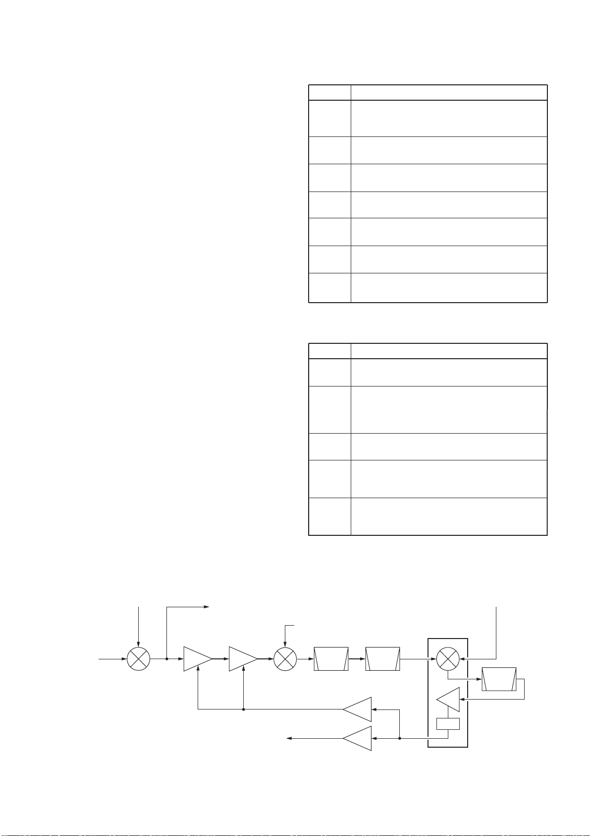
3-5-1 SCOPE RECEIVER CIRCUIT (RF-B UNIT)
A portion of the 64.455 MHz 1st IF signal from the 1st
mixer circuit (Q1203–Q1206: while receiving) or IF amplifier (Q1551: while transmitting) is passed through the
PIN attenuator (Q2203) and amplified at the IF amplifiers (Q2202, Q2201), and then mixed with the 77.8 MHz
scope 2nd LO (S2LO) signal at the mixer circuit (D2101)
to produce the 13.345 MHz IF signal. The mixed IF signal
is passed through the ceramic bandpass filters (FI2003,
FI2002) to suppress unwanted signals. The filtered IF signal is applied to the FM IF IC (IC2001, pin 16).
The applied 13.345 MHz IF signal is mixed with the sweep
LO (S3LO) signals from the PLL unit at the FM IF IC
(IC2001). The mixed IF signals are filtered at the ceramic
bandpass filter (FI2001) then applied to the limiter amplifier section in the FM IF IC (IC2001, pin 5). The applied IF
signals are converted into DC voltages according to the
applied IF signal strength at the RSSI section in the IC.
The converted voltages are output from pin12 (IC2001) and
amplified at IC2002, then applied to the MAIN-A unit as the
SCPL signal.
3-6 POWER SUPPLY CIRCUITS
3-6-1 PA UNIT
LINE
PHV
HV
14V
14VA
a8V
5V
H5V
The voltage from an external power supply via
the common filter circuit (FILTER-A unit; L501,
L502).
The same voltage as the PHV line passed
through a fuse (F1).
The same voltage as the HV line passed
through the switching relay (RL1).
The same voltage as the 14 V line is applied to
the AF power amplifier (MAIN-A unit; IC332).
Common 8 V converted from the 14 V line and
regulated by the +8 regulator circuit (IC3).
Common 5 V converted from the 14 V line and
regulated by the +5 regulator circuit (IC2).
Common 5 V converted from the HV line and
regulated by the H5V regulator circuit (IC1).
DESCRIPTION
Some of the DC voltages from the FM IF IC (IC2001) are
amplified at IC2002 to produce AGC voltages for the IF
amplifiers (Q2201, Q2202), producing wider dynamic range.
By sweeping LO signals (S3LO) are applied to the mixer
section in the FM IF IC (IC2001), the spectrum scope function is activated.
3-5-2 SWEEP LO CIRCUIT (PLL UNIT)
The sweep LO signals (S3LO) are generated by the DDS
IC (IC801) using the 32 MHz system clock. A 10-bit digital
signal is converted into analog wave signals at the D/A converter (R801–R820). The converted analog wave is passed
through the bandpass filter (L802, L803, C809–C813) then
applied to the RF-B unit via (J801) after being amplified at
the buffer amplifier (Q802).
• SCOPE CIRCUIT DIAGRAM
1st LO
signal
to 2nd mixer circuit
3-6-2 FRONT UNIT
LINE
5VF
–15V
–7V
–8V
+18V
Common 5 V converted from the 14 V line and
regulated by the +5 regulator circuit (IC861).
Common –15 V converted from the 14 V line
and converted by the –15 DC-DC converter circuit (IC841, Q841, D841). The voltage is applied
to the –7 V, –8 V regulator circuits and etc.
Common –7 V converted from the –15 V line
and regulated by the –7 regulator circuit (IC501).
Common –8 V converted from the –15 V line
and regulated by the –8V regulator circuit
(IC881).
Common 18 V converted from the 14 V line and
converted by the 18 V DC-DC converter circuit
(IC821, Q821, D822).
DESCRIPTION
S3LO signal
(12.79–12.99 MHz*)
RF signals
1st mixer A
Q1203–Q1206
RF-B unit
Q2202
IF
amp.
Q2201
IF
amp.
D2101 FI2003 FI2002
to the MAIN-A unit
S2LO signal
(77.80 MHz)
SCPL signal
3 - 9
Ceramic
BPF
IC2002b
AGC
amp.
IC2002a
Ceramic
BPF
IC2001
Mixer
16
Limiter
amp.
RSSI
12
*depending on sweeping passband width
2
3
5
FI2001
Ceramic
BPF
Page 18
3-6-3 MAIN-A UNIT
LINE
R8V
T8V
Receive 8 V converted from the 14 V line and
regulated by the R8V regulator circuit (Q601,
Q602, D601).
Transmit 8 V converted from the 14 V line and
regulated by the T8V regulator circuit (Q611,
Q612, D611).
DESCRIPTION
3-6-4 CTRL-A AND PLL UNITS
LINE
5V
5V
Common 5 V for the antenna tuner CPU
(CTRL-A unit; IC5), EEPROM (CTRL-A unit;
IC6) and etc. converted from the 14 V line and
regulated by the +5 regulator circuit (CTRL-A
unit; IC13).
Common 5 V for each PLL-A and PLL-B circuits
regulated from the 8 V line and regulated by
the +5 regulator circuit (PLL unit; IC382: PLL-A,
IC682: PLL-B).
DESCRIPTION
3-7 LOGIC CIRCUITS
3-7-1 BAND SELECTION DATA
(RF-B, CTRL-A, PLL UNITS)
Frequency
[MHz]
IC401–IC403
(RF-B )
0.03–1.5999999 B0
1.6–1.999999 B1
2.0–2.999999 B2
4.0–4.999999
5.0–5.999999
B4
6.0–6.999999 B5W
7.0–7.299999 B5
7.3–7.999999 B5W
8.0–10.999999 B6
11.0–11.999999
12.0–13.999999
B7W
14.5–14.999999 B7W
15.0–19.999999
20.0–20.999999
B8W
21.0–21.499999 B8
21.5–21.999999 B8W
22.0–29.999999 B9 L7S
30.0–44.999999
45.0–49.999999
B10W
54.0–60.000000 B10W
IC11
(CTRL-A)
L1S
L2S3.0–3.999999 B3
L3S
L4S
L5S14.0–14.499999 B7
L6S
L8S
IC101
(PLL)
IC401
(PLL)
VA1S VB1S
VA2S VB2S
VA3S VB3S
VA4S VB4S50.0–54.000000 B10
3-7-2 SUB-CPU PORT ALLOCATIONS
(DISPLAY BOARD; IC401)
Pin Port
number name
7, 8
12, 83
56, 57
64–66
OSC1,
OSC2
DRES
9
MSB,
MSA
DOTK,
DSHK
MDM0–
MDM2
TNRD, MOND
NBD, NRD
67–75
LOCD, TXD
RXD, PBTD
NOTD
77, 79
81
82, 84
85, 88
86
87
92
93
94
95
96
97
98
99
100
PB1B,
PB1A
METV
RSA,
RSB
PB2A,
PB2B
LMFD
LFMD
BALL
NRL
MIGL
PWRL
CMPL
KYSL
DELL
NOTL
PITL
Input and output ports for the system
clock oscillator (X401; 9.8304 MHz).
Input port for the reset signal.
Input port for the [DIAL]; pulse-type
signals are applied.
Input ports for the [ELEC-KEY] jack.
Output ports for the S/RF meter backlight and function switch activation
indicator brightness control signal.
Port
MDM0
MDM1
MDM2
Control signal output ports for the
activation indicator of function switches.
High : When the function is activated.
Input port for the [TWIN PBT (inner)]
control (PBT board, S1/inner).
Outputs the S/RF meter (ME1) drive
signal.
Input ports for the [RIT/∆TX] control;
pulse-type signals are applied.
Input port for the [TWIN PBT(outer)]
control (PBT board, S1/outer).
Input port for data signal from the
main-CPU (MAIN-A unit; IC3501).
Outputs data signal for the main-CPU
(MAIN-A unit; IC3501).
A/D input port for the [BAL] control
(R702/ inner).
A/D input port for the [NR] control
(R702/ outer).
A/D input port for the [MIC GAIN]
control (R712).
Input port for the [RF POWER] control (R714).
Input port for the [COMP] control
(R716).
Input port for the [KEY SPEED] control (R718).
Input port for the [BK-IN DELAY] control (R720).
Input port for the [NOTCH] control
(PBT board, R1/inner).
Input port for the [CW PITCH] control
(PBT board, R1/outer).
Description
Backlight level
1234567
High
Low High
High High High HighLow Low Low
Low Low Low
Low High HighLow
High High High High
3 - 10
Page 19

3-7-3 MAIN-CPU PORT ALLOCATIONS
(MAIN-A UNIT; IC3501)
Pin Port
number name
29
30
31
32
34
37
59
61
63
64
66
69
70
71
72
73
74
75
76
77
A0–A3,
A4–A11,
A12–A18
SKYS
RTKI
DPGI
DSDR
PWRK
DSKY
DB0–DB3,
DB4–DB11
DB12–DB15
CTXD
CRXD
MCK
MDAT
TRVI
IKEY
RXS
TXS
ISTA
DRES
UNLC
PSTB
PSEL
CON2
6–9,
11–18,
20–26
40–43,
45–52,
54–57
Address signal output ports for the
LCD controller (IC3551).
Input port for the [KEY] jack.
Low : During key down
Input port for the RTTY keying.
Power supply detection input port for
the DSP-A board.
Input port for data signal from DSP-A
board.
Input port for the [POWER] switch.
Low : When the [POWER] is pushed.
Outputs CW/RTTY keying.
Data bus lines for the LCD controller
,
(IC3551) and I/O expander (IC3652–
IC3654).
Outputs the CI-V signal.
Input port for the CI-V signal.
Outputs clock signal.
Outputs data signal.
Input port for the [XVERT] detection
signal.
Input port for transmit control signal
from the antenna tuner CPU (CTRL-A
board; IC5).
Outputs R8V regulator (Q601, Q602,
D601) control signal.
Low : While receiving
Outputs T8V regulator (Q611, Q612,
D611) control signal.
Low : While transmitting
Outputs antenna tuner start signal.
Outputs reset/inhibit signal to the subCPU (DISPLAY board; IC401), DDS
ICs (PLL unit; IC101, IC401), antenna
tuner CPU (CTRL-A board; IC5), and
etc.
Input port for unlock signal from the
PLL unit.
Outputs strobe signals for the I/O
expander IC (PLL unit; IC1).
Outputs strobe selection signals for
the I/O expander (PLL unit; IC1).
Outputs control signal for the DDS circuits (PLL unit; IC101, IC401).
Description
Pin Port
number name
78
79
85, 86
96
97
98
101
105
106
107
108
109
110
111
112
115
116
CON1
(PDAT)
CON0
(PCK)
XTAL,
EXTAL
LRES
LTXD
LRXD
TMD
SCPL
VOXL
AVXL
ASO0
ASO1
ASO2
STON
BEEP
SENI
PWRS
Description
Outputs data signal for the DDS circuits (PLL unit; IC101, IC401).
Outputs clock signal for the DDS circuits (PLL unit, IC101, IC401).
Input ports for the CPU system clock
oscillator (X3501; 19.6608 MHz).
Outputs reset/inhibit signal for the
LCD controller (IC3551), I/O expander
(IC3652–IC3654), and etc.
Outputs data signal for the sub-CPU
(DISPLAY board; IC401).
Input port for data signal from the
sub-CPU (DISPLAY board; IC401).
Outputs [TIMER] indicator control signal.
High : When the timer function is ON
Input port for the scope signal.
A/D input port for the VOX gain.
A/D input port for the anti-VOX level.
A/D input port via the analog switch
(IC3631) for the SML signal from the
S-meter amplifier circuit (IC101a),
and ALCL signal from the ALC meter
amplifier circuit (IC551a).
A/D input port via the analog switch
(IC3631) for the NSQO signal from
the level conveter (DSP-A board;
IC2063), for noise squelch operation, and FORL signal from the power
meter amplifier circuit (IC571a).
A/D input port from the analog switch
(IC3631) for the FNTL signal from
the low-pass filter (DSP-A board;
IC2472a), for tone squelch operation,
and REFL signal from the SWR meter
amplifier circuit (IC571b).
Outputs CW side-tone signals.
Outputs beep audio signals.
Input port for connected microphone’s
PTT switch and SEND signal from the
ACC jacks.
High : While PTT switch is pushed or
activated from an external unit.
Outputs control signal for the power
switching relay (PA unit; RL1) .
High : During power ON
3 - 11
Page 20

3-7-4 INPUT EXPANDER ALLOCATIONS
(1) DISPLAY board; IC411
Pin Port
number name
1
5
12
13
14, 15
KI4
MUDK
KI3
KI0
KI1, KI2
Input port for the [RIT], [∆TX] and
[CLEAR] switches.
Input port for [UP] and [DN] switches
of the connected microphone.
Input port for the [DUALWATCH],
[CHANGE], [V/M] and [M/S] switches.
Input port for the [TUNER],
[MONITOR], [NB] and [NR] switches.
Input ports for the multi-function
switches.
Description
(2) MAIN-A unit; IC3652
Pin Port
number name
11
12
13
14
16
17
18
CTFL
RTDT
EKEY
TCON
VINT
VRAC
SBSY
Input port transmission status for CW
Input port for RTTY decode data.
Input port for the KEY signal from the
connected AH-3.
Low : While tuning or tune NG
Input port for AH-3 connection detection.
High : When AH-3 is connected.
Input port for interrupting signal
from audio recoder.
Input port for address clock signal
from audio recoder.
Input port for busy signal from
the installed UT-102 SPEECH
SYNTHESIZER.
Description
3-7-5 OUTPUT EXPANDER ALLOCATIONS
(1) PLL unit; IC1
Pin Port
number name
4
5
6
7
12
13
14
PST1
PST2
PST3
PST4
PST5
PST6
PST7
Outputs strobe signals to DDS IC
(IC101) for the 1st LO PLL A circuit.
Outputs strobe signals to PLL IC
(IC381) for the 1st LO PLL A circuit.
Outputs strobe signals to DDS IC
(IC401) for the 1st LO PLL B circuit.
Outputs strobe signals to PLL IC
(IC681) for the 1st LO PLL B circuit.
Outputs strobe signals to DDS IC
(IC701) for the 3rd LO PLL circuit.
Outputs strobe signals to PLL IC
(IC901) for the S2 LO PLL circuit.
Outputs strobe signals to DDS IC
(IC801) for the S3 LO PLL circuit.
Description
(2) PLL unit; IC101
Pin Port
number name
66
68
70
71
73
74
75
MAKS
PAMT
PAFS
VA4S
VA3S
VA2S
VA1S
(3) PLL unit; IC401
Pin Port
number name
68
70
71
73
74
75
PBMT
PBFS
VB4S
VB3S
VB2S
VB1S
Description
Outputs the marker mute switch
(IC192) control signa
High : When the marker ON is select-
ed.
Outputs LO mute switch (Q361) control signal.
Low : Muted
Outputs bandpass filter select switch
(Q351) control signal.
High : When less than 8 MHz is dis-
played on the main band.
Outputs the LO switch (Q121) control
signal.
High : While 45.0–60.0 MHz band is
displayed on the main band.
Outputs the LO switch (Q122) control
signal.
High : While 20.0–44.999999 MHz band
is displayed on the main band.
Outputs the LO switch (Q123) control
signal.
High : While 8.0–19.999999 MHz band
is displayed on the main band.
Outputs the LO switch (Q126) control
signal.
High : While 0.03–7.999999 MHz band
is displayed on the main band.
Description
Outputs LO mute switch (Q661) control
signal.
Low : Muted
Outputs bandpass filter select switch
(Q651) control signal.
High : When less than 8 MHz is dis-
played on the main band.
Outputs the LO switch (Q421) control
signal.
High : While 45.0–60.0 MHz band is
displayed on the main band.
Outputs the LO switch (Q422) control
signal.
High : While 20.0–44.999999 MHz band
is displayed on the main band.
Outputs the LO switch (Q423) control
signal.
High : While 8.0–19.999999 MHz band
is displayed on the main band.
Outputs the LO switch (Q426) control
signal.
High : While 0.03–7.999999 MHz band
is displayed on the main band.
l.
3 - 12
Page 21

(4) CTRL-A board; IC11
Pin Port
number name
Outputs a low-pass filter select signal.
High : When 0.03–1.999999 MHz
Outputs a low-pass filter select signal.
High : When 2.0–4.999999 MHz band
Outputs a low-pass filter select signal.
High : When 5.0–7.999999 MHz band
Outputs a low-pass filter select signal.
High : When 8.0–11.999999 MHz
Outputs a low-pass filter select signal.
High : When 30.0–60.0 MHz band is
Outputs a low-pass filter select signal.
High : When 22.0–29.999999 MHz
Outputs a low-pass filter select signal.
High : When 15.0–21.999999 MHz
Outputs a low-pass filter select signal.
High : When 12.0–14.999999 MHz
11
12
13
14
4
5
6
7
L1S
L2S
L3S
L4S
L8S
L7S
L6S
L5S
Description
band is selected.
is selected.
is selected.
band is selected.
selected.
band is selected.
band is selected.
band is selected.
(6) RF-B unit; IC402
Pin
number
4 B7WS
5 B7S
6 B8WS
7 B8W
12 B10S
13 B10WS
14 B9S
Port
name
Outputs a bandpass filter select signal.
High : When 11–13.999999 MHz or
Outputs a bandpass filter select signal.
High : When 14.0–14.499999 MHz is
Outputs a bandpass filter select signal.
High : When 15.0–20.999999 MHz or
Outputs a bandpass filter select signal.
High : When 21.0–21.499999 MHz is
Outputs a bandpass filter select signal.
High : When 50.0–54.0 MHz is select-
Outputs a bandpass filter select signal.
High : When 30.0–49.999999 MHz or
Outputs a bandpass filter select signal.
High : When 22–29.999999 MHz is
Description
14.5–14.999999 MHz band is
selected.
selected.
21.5–21.999999 MHz band is
selected.
selected.
ed.
54.000001 MHz band is selected.
selected.
(5) RF-B unit; IC401
Pin
number
4 B0S
5 B1S
6 B2S
7 B3S
11 B6S
12 B5S
13 B5WS
14 B4S
Port
name
Outputs a bandpass filter select signal.
High : When 0.03–1.599999 MHz is
Outputs a bandpass filter select signal.
High : When 1.6–1.999999 MHz is
Outputs a bandpass filter select signal.
High : When 2.0–2.999999 MHz is
Outputs a bandpass filter select signal.
High : When 3.0–3.999999 MHz is
Outputs a bandpass filter select signal.
High : When 8.0–10.999999 MHz is
Outputs a bandpass filter select signal.
High : When 7.0–7.299999 MHz is
Outputs a bandpass filter select signal.
High : When 6.0–6.999999 MHz or
Outputs a bandpass filter select signal.
High : When 4.0–5.999999 MHz is
Description
selected.
selected.
selected.
selected.
selected.
selected.
7.3–7.999999 MHz band is
selected.
selected.
(7) RF-B unit; IC403
Pin
number
4 AT1S
5 AT2S
6 PR1S
7 PR2S
Port
name
Outputs control signal for the
attenuator circuit (RL102, R102,
R106, R111).
Low : When 6 dB attenuator is ON.
Outputs control signal for the
attenuator circuit (RL103, R112,
R113, R114).
Low : When 12 dB attenuator is ON.
Outputs control signal for the preamplifier (PRE-AMP board; Q4201,
Q4202).
High : When P.AMP 1 is ON.
Outputs control signal for the preamplifier (PRE-AMP board; Q4302).
High : When P.AMP 2 is ON.
Output the RX antenna select
14 RANS
signal.
High : When RX antenna is selected.
Description
3 - 13
Page 22

(8) MAIN-A unit; IC3653
Pin Port
number name
Outputs strobe signals for the out-
13
14
15
16
17
18
19
BSTB
ANTS
FSTB
ASTB
MSTB
AFMS
SQLS
put expander ICs (RF-B unit; IC301,
IC302).
Outputs the antenna connector
([ANT1] or [ANT2]) select signal.
High : When the [ANT2] is selected.
Outputs strobe signals for the output
expander (CTRL-A board; IC11).
Outputs strobe signals for the D/A
converter (IC3751).
Outputs strobe signals for the output
expander ICs (IC3752, IC3753).
Outputs control signal for the AF mute
switch (IC331).
High : When the [AF] control is set to
Outputs squelch mute control signal,
applied to the squelch gate (IC301).
High : When squelch is closed.
(9) MAIN-A unit; IC3654
Pin Port
number name
Outputs squelch control signal for the
12
13
14
15
16
17, 18
SQSS
SPS
SSTB
VCS
ESTA
DSFR,
DSFW
[MIC] and [ACC1] connectores.
High : Squlch opend. (RX LED ON)
Outputs control signal for the internal
speaker ON/OFF select relay (RL351).
High : Internal speaker is ON.
Outputs strobe signals for the optional
UT-102 SPEECH SYNTHESIZER.
Outputs chip select signal for the
audio recoder (IC3001).
Outputs external antenna tuner (AH-3)
start signal.
Low : When the [TUNE] switch is
Outputs control signal for the DSP IC
(DSP-A board; IC2001).
Description
maximum counter clockwidth.
Description
pushed.
(10) MAIN unit; IC3752
Pin Port
number name
Outputs control signal for the noise
4
6
7
12
14
NBS
MSL1
MSL2
VOSL
MISL
blanker switch (Q3751, Q3752).
High : When the [NB] switch is ON,
Outputs audio select signal for the TX
monitor function.
High : During monitoring in SSB or
Outputs audio select signal for the TX
monitor function.
High : During monitoring in AM or FM
Outputs analog switch (IC3005) control signal for the audio recoder’s
(IC3001) output.
High : When the audio recoder’s out-
Outputs analog switch (IC3002) control signal for input of the microphone
amplifier (IC461).
High : Except the microphone input is
(11) MAIN-A unit; IC3753
Pin Port
number name
Outputs AM mode select signal for
4
5
6
7
11
14
AMS
PHFS
P50S
MODS
DSRS
FMNS
the AGC and APC circuit.
High : When AM is selected.
Outputs HF band RF power control
signal.
High : When 0.03–29.999999 MHz
Outputs 50 MHz band RF power control signal.
High : When 30–60 MHz band is
Outputs 2nd IF filter (FI131 or FI133)
select signal.
High : When transmitting in AM or FM
Outputs reset signal for the DSP circuit and etc.
Outputs FM deviation control signal.
High : When FM-N is selected.
Description
except in FM mode.
RTTY mode.
mode.
put to the AF circuit.
selected.
Description
band is selected.
selected.
mode. (FI131 is ON)
3 - 14
Page 23
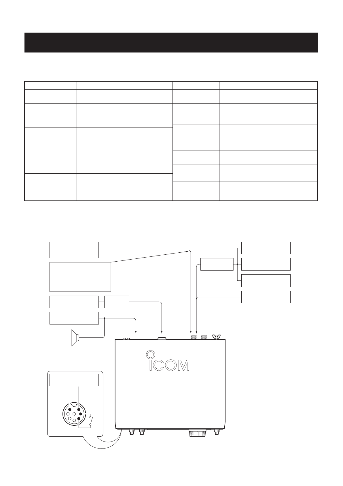
SECTION 4 ADJUSTMENT PROCEDURES
4-1 PREPARATION
■
REQUIRED TEST EQUIPMENT
EQUIPMENT GRADE AND RANGE EQUIPMENT GRADE AND RANGE
DC power supply
RF power meter
(terminated type)
Frequency counter
RF voltmeter
Modulation analyzer
Distortion meter
Oscilloscope
Output voltage
Current capacity
Measuring range
Frequency range
Impedance
SWR
Frequency range
Frequency accuracy
Sensitivity
Frequency range
Measuring range
Frequency range
Measuring range
Frequency range
Measuring range
Frequency range
measuring range
: 13.8 V
: 30 A or more
: 10–200 W
: 1.8–100 MHz
: 50
Ω
: Less than 1.2 : 1
: 0.1–100 MHz
: ±0.5 ppm or better
: 100 mV or better
: 0.1–100 MHz
: 0.01–10 V
: At least 90 MHz
: 0–100%
: At least 90 MHz
: 0–100%
: DC–20 MHz
: 0.01–20 V
Audio generator
Standard signal
generator (SSG)
AC millivoltmeter Measuring range : 10 mV–10 V
DC voltmeter Input impedance : 50 kΩ/V DC or better
DC ammeter Measuring range : 1 A/30 A
Spectrum analyzer
Attenuator
External speaker
Frequency range
Measuring range
Frequency range
Output level
Measuring range
Spectrum bandwidth
Power attenuation
Capacity
Resistance
Capacity
: 300–3000 Hz
: 1–500 mV
: 0.1–300 MHz
: 0.1 µV to 32 mV
(–127 to –17 dBm)
: At least 90 MHz
: 100 kHz or more
: 50 or 60 dB
: 150 W or more
: 8
Ω
: 5 W or more
■ CONNECTIONS
Standard signal
generator
CAUTION !
DO NOT transmit while
an SSG is connected to
the antenna connector.
DC power supply Ammeter
Distortion meter
Speaker
Audio generator
to [EXT SP]
to [DC 13.8 V]
Attenuator
to the antenna connector
[ANT1] [ANT2]
FM deviation meter
Modulation analyzer
Spectrum analyzer
RF power meter
[MIC]
PTT
4 - 1
Page 24

4-2 PLL ADJUSTMENTS
ADJUSTMENT ADJUSTMENT CONDITION
MEASUREMENT
VALUE
ADJUSTMENT
POINT
UNIT LOCATION UNIT ADJUST
L52
REFERENCE
FREQUENCY
LPL-A LOCK
VOLTAGE
VCO-A LOCK
VOLTAGE
1LO-A
OUTPUT
LEVEL
LPL-B LOCK
VOLTAGE
VCO-B LOCK
VOLTAGE
1LO-B
OUTPUT
LEVEL
3LO
OUTPUT
LEVEL
S3LO
OUTPUT
LEVEL
• Display freq. : Any
1
• Turn L52 on the PLL unit to 4 rotation downside for presetting.
• Receiving
2
• Display freq. : 0.030000 MHz
1
• Mode : USB
• Receiving
• Display freq.
1
• Mode : USB
• Receiving
2
• Display freq.
• Mode : USB
• Receiving
3
• Display freq.
• Mode : USB
• Receiving
4
• Display freq.
• Mode : USB
• Receiving
1
• Display freq.
0.030000 MHz, 7.999999 MHz
8.000000 MHz, 19.999999 MHz
20.000000 MHz, 44.999999 MHz
45.000000 MHz, 60.000000 MHz
• Receiving
1
• Sub display freq. : 0.030000 MHz
• Mode : USB
• Receiving
1
• Sub display freq.
• Mode : USB
• Receiving
2
• Sub display freq.
• Mode : USB
• Receiving
3
• Display freq.
• Mode : USB
• Receiving
4
• Display freq.
• Mode : USB
• Receiving
1
• Sub display freq.
0.030000 MHz, 7.999999 MHz
8.000000 MHz, 19.999999 MHz
20.000000 MHz, 44.999999 MHz
45.000000 MHz, 60.000000 MHz
• Receiving
1
• Display freq.
• Receiving
1
• Display freq.
• Receiving
: 7.999999 MHz
: 19.999999 MHz
: 44.999999 MHz
: 60.000000 MHz
:
: 7.999999 MHz
: 19.999999 MHz
: 44.999999 MHz
: 60.000000 MHz
:
: Any
: Any
Connect a frequency
PLL
counter to the check
point P81.
Connect an RF voltmeter to the check
point P81.
Connect a digital
PLL
multimeter or oscilloscope to the check
point LPA.
Connect a digital
PLL
multimeter or oscilloscope to the check
point LVA.
Connect an RF volt-
PLL
meter to the check
point P351.
Connect a digital
PLL
multimeter or oscilloscope to the check
point LPB.
Connect a digital
PLL
multimeter or oscilloscope to the check
point LVB.
Connect an RF volt-
PLL
meter to the check
point P651.
Connect an RF volt-
PLL
meter to the check
point P701.
Connect an RF volt-
PLL
meter to the check
point P801.
64.000000 MHz
Maximum level
(0 dB or more)
2.0 V
4.3 V
4.3 V
4.3 V
4.3 V
–2 dBm or more
2.0 V
4.3 V
4.3 V
4.3 V
4.3 V
–2 dBm or more
–16 dBm or more
–10 dBm or more
PLL
PLL
PLL
PLL
PLL
(R33
for critical
adjustment)
L81, L82
C154
C278
C258
C228
C208
Verify
C454
C578
C558
C528
C508
Verify
Verify
Verify
4 - 2
Page 25
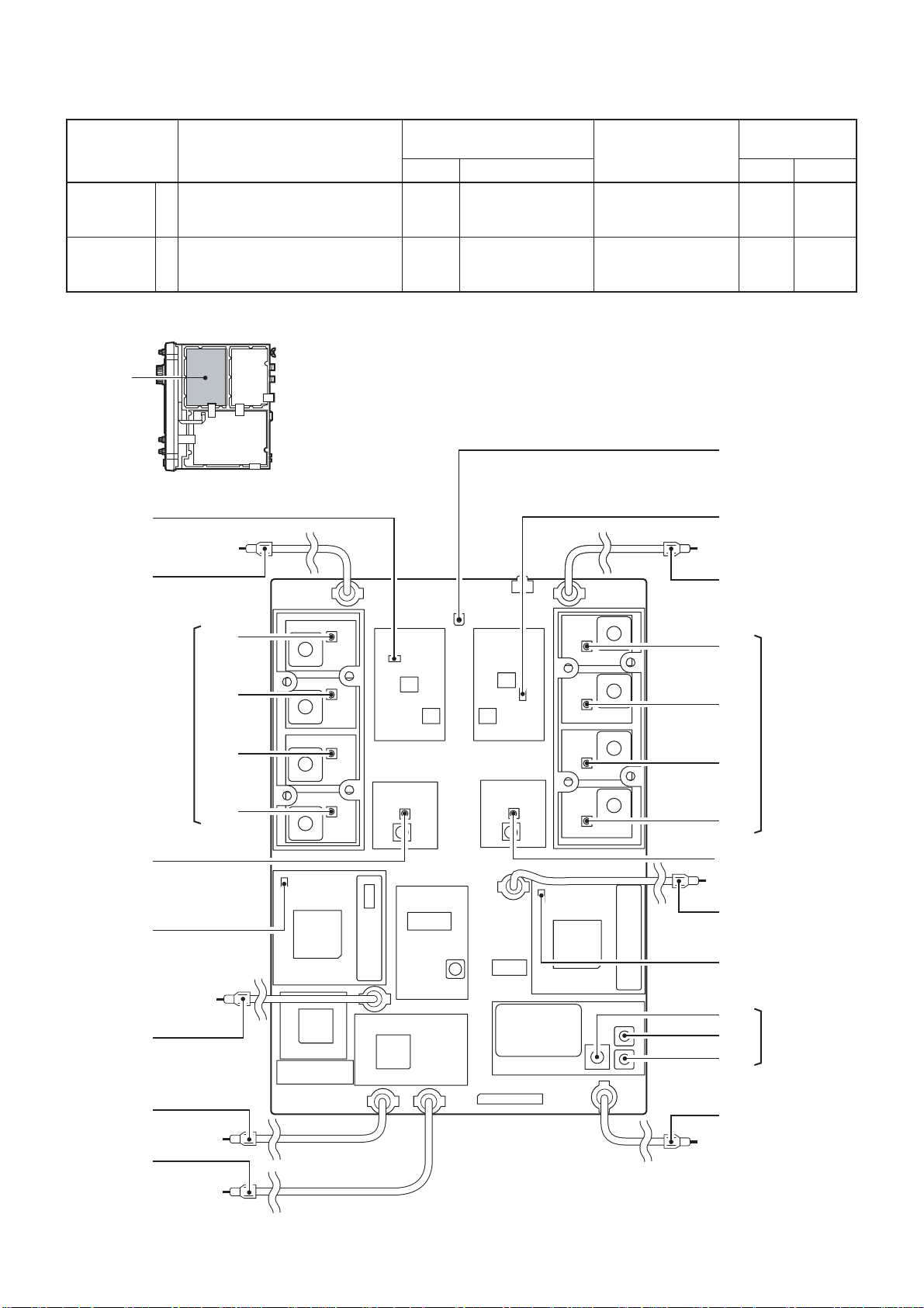
PLL ADJUSTMENTS—continued
ADJUSTMENT ADJUSTMENT CONDITION
MEASUREMENT
VALUE
ADJUSTMENT
POINT
UNIT LOCATION UNIT ADJUST
S2LO
OUTPUT
LEVEL
MARKER
OUTPUT
LEVEL
11• Display freq.
• Receiving
• Display freq.
• Receiving
: Any
: Any
PLL
Connect an RF voltmeter to the check
point P901.
PLL
Connect an oscilloscope to the check
point P851.
–3 dBm or more
4 Vp-p or more
Verify
Verify
• PLL unit
PLL unit
R33
Reference
Bottom view of the transceiver
LVB
VCO-B lock voltage
check point
P651
1LO-B output level
check point
C508
frequency
adjustment
LVA
VCO-A lock voltage
check point
P361
1LO-A output level
check point
C278
VCO-B
C528
lock voltage
adjustment
C558
C578
C454
LPL-B lock voltage
adjustment
LPB
LPL-B lock voltage
check point
P901
S2LO output level
check point
P801
3LO output level
check point
P701
S3LO output level
check point
C258
VCO-A
lock voltage
adjustment
C228
C208
C154
LPL-A lock voltage
adkustment
P851
Marker output level
check point
LPA
LPL-A lock voltage
check point
L52
L81
L82
Reference
frequency
adjustment
P81
Reference frequency
check point
4 - 3
Page 26
4-3 TRANSMITTER ADJUSTMENTS
ADJUSTMENT ADJUSTMENT CONDITION
IDLING
CURRENT
(for drive)
(for fi nal
amplifi er)
TX PEAK 1 • Display freq. : 14.100000 MHz
TRANSMITTER
TOTAL GAIN
1
• Display freq. : 14.100000 MHz
• Mode : CW (Key up)
• Preset R11, R18 on the PA unit to
max. CCW
• [RF POWER] : Max. CW
• [TUNER] : OFF
• Transmitting (without key)
After adjustment, re-solder the wire (W29) on the PA board
2 • Transmitting (without key) PA Unsolder R28 (L8
After adjustment, re-solder the wire (W29) on the PA board
• Mode : USB
• Set following selections, controls
and functions as :
[VOX] : OFF , [ TX] : OFF
PBT1 : Center , PBT2 : Center
Filter : 2.4 kHz
[RF POWER] : Max. CW
[MIC GAIN] : Center
[TUNER] : OFF
[METER] : METER Po
[MONITOR] : OFF
• Apply no audio signals to [MIC]
connector.
• Transmitting
2• Connect an audio generator to
[MIC] connector and set as:
Frequency : 1.5 kHz
Level : 1 mVrms
• Transmitting
3 • Transmitting Maximum output
4 • [MIC GAIN] : Center
• Preset L1701, L1702's top to same
high with coil's case.
• Connect an audio generator to
[MIC] connector and set as:
Frequency : 1.5 kHz
Level : 10 mVrms
• Transmitting
Adjust in sequence L1801, L1553, L1702, L1701, L1702, L1701
1 • Display freq. : 14.100000 MHz
• Mode : USB
• [MIC GAIN] : Center
• Connect an audio generator to
[MIC] connector and set as:
Frequency : 1.5 kHz
Level : 1 mVrms
• Transmitting
MEASUREMENT
VALU E
ADJUSTMENT
POINT
UNIT LOCATION UNIT ADJUST
PA Unsolder W29.
Connect an ammeter to
the unsoldering points
of W29.
side).
Connect an ammeter to
the unsoldering points
of R28.
MAIN-A Connect a digital
multimeter or oscilloscope to the check
point CP243.
Rear
Connect an RF power
panel
RF-B Connect an RF volt-
panel
meter to [ANT1] connector.
meter the check point
J201.
Rear
Connect an RF power
meter to [ANT1] connector.
250 mA PA R11
500 mA PA R18
0.06 V MAIN-A R247
50 W Front
panel
MAIN-A L261
power
Maximum level RF-B L1801,
50 W MAIN-A R263
[MIC GAIN]
control
L1553,
L1702,
L1701
4 - 4
Page 27
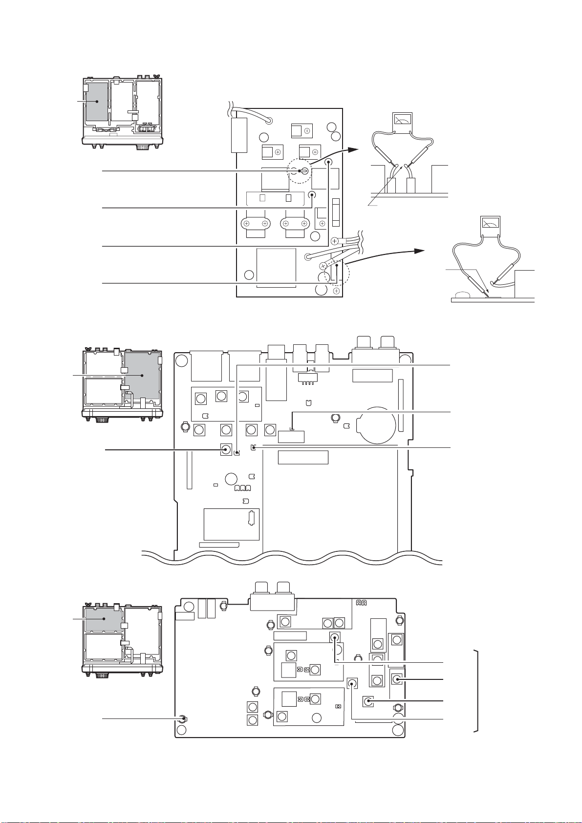
• PA unit
PA unit
Top view of the transceiver
W29
Idling current check point
for drivers
R18
Idling current adjustment
for finals
R11
Idling current adjustment
for drivers
R28
Idling current check point
for finals
• MAIN-A unit
MAIN-A
unit
Bottom view of the transceiver
L261
TX peak adjustment
Ammeter
W29
L4
Unsoldering here
Unsoldering here
RL1
Ammeter
R263
Transmitter
total gain
adjustment
CP243
TX peak
check point
R247
TX peak
adjustment
• RF-B unit
RF-B
unit
Bottom view of the transceiver
J201
TX peak check point
4 - 5
L1553
L1801
L1702
L1701
TX peak
adjustment
Page 28

TRANSMITTER ADJUSTMENTS—continued
ADJUSTMENT ADJUSTMENT CONDITION
MEASUREMENT
VALUE
UNIT LOCATION UNIT ADJUST
Ic APC
HF BANDS
OUTPUT
POWER
50 MHz BAND
OUTPUT
POWER
FM
DEVIATION
AM
CARRIER
POWER
AM
MODULATION
• Display freq. : 3.550000 MHz
1
• Mode : RTTY
• Connect CP501 to GND.
• Transmitting
• Display freq. : 14.100000 MHz
1
• Mode : RTTY
• [RF POWER] : Max. CW
• [TUNER] : OFF
• Transmitting
• Display freq. : 51.000000 MHz
1
• Mode : RTTY
• [RF POWER] : Max. CW
• [TUNER] : OFF
• Transmitting
1
• Display freq. : 29.60000 MHz
• Mode : FM
• Filter : 15 kHz
• [RF POWER] : Max. CW
• [MIC GAIN] : Center
• Connect an audio generator to
[MIC] connector and set as:
Frequency : 1 kHz
Level : 10 mVrms
• Transmitting
1
• Display freq. : 14.100000 MHz
• [RF POWER] : Max. CW
• Mode : AM
• [MIC GAIN] : Center
• Apply no audio signals to [MIC]
connector.
• Transmitting
1
• Display freq. : 14.10000 MHz
• Mode : AM
• [MIC GAIN] : Center
• [RF POWER] : Max. CCW
• Connect an audio generator to
[MIC] connector and set as:
Frequency : 1 kHz
Level : 10 mVrms
Rear
panel
Rear
panel
Rear
panel
Rear
panel
Rear
panel
Rear
panel
Connect an ammeter between power
supply and the
IC-756PROIII.
Connect an RF
power meter to
[ANT1] connector.
Connect an RF
power meter to
[ANT1] connector.
Connect an FM deviation meter to [ANT1]
connector through an
attenuator.
Connect an RF
power meter to
[ANT1] connector.
Connect a modulation analyzer to
[ANT1] connector through an
attenuator.
23 A
105 W
100 W
±4.5 kHz
40 W
90%
ADJUSTMENT
POINT
MAIN-A
MAIN-A
MAIN-A
DSP-A
MAIN-A
DSP-A
R545
R507
R509
R2227
R510
R2229
4 - 6
Page 29
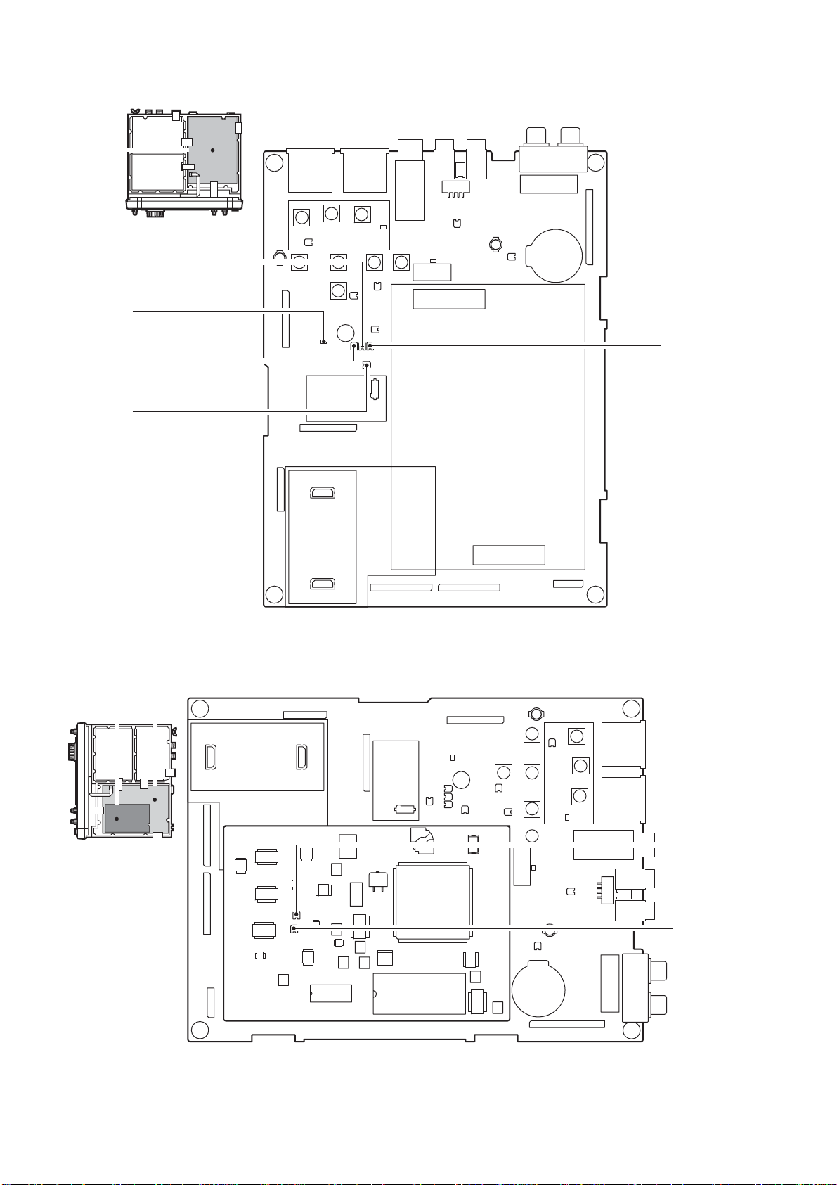
• MAIN-A unit
MAIN-A
unit
Bottom view of the transceiver
R509
50 MHz band output power
adjustment
CP501
Ic APC check point
R507
HF bands output power
adjustment
R545
Ic APC adjustment
R510
AM carrier
adjustment
• DSP-A board
DSP-A board
MAIN-A
unit
Bottom view
of the transceiver
R2227
FM deviation
adjustment
R2229
AM modulation
adjustment
4 - 7
Page 30

4-4 RECEIVER ADJUSTMENTS
MEASUREMENT
ADJUSTMENT ADJUSTMENT CONDITION
UNIT LOCATION UNIT
RX PEAK 1 • Display freq. : 14.100000 MHz
• [DUALWATCH] : OFF
• Mode : USB
• Set following selections, controls
and functions as:
[AGC] : MID [ATT] : OFF
[NB] : OFF [RIT] : OFF
PBT1 : Center PBT2 : Center
Filter : 2.4 kHz
[P.AMP] : P.AMP1
[RF/SQL] : Center
[NOTCH] : OFF
[NR] switch : OFF
• Preset center dots to 90˚ difference on the roter and stater of
C1036 and C1211.
• Connect an SSG to [ANT1] connector and set as:
Frequency : 14.101500 MHz
Level : 10 µV* (–87 dBm)
Modulation : 1 kHz/±5.0 kHz dev.
• Receiving
Adjust L211 to upper side of 2 peak points.
2 • Sub display freq. : 14.100000 MHz
• [DUALWATCH] : ON
• Mode : USB
• [BAL] : Max. CW
• Set an SSG as:
Level : 10 µV* (–87 dBm)
• Receiving
Adjust L1011 to upper side of 2 peak points.
FM
DISTORTION
MIXER
BALANCE
*This output level of standard signal generator (SSG) is indicated as SSG's open circuit.
1 • Display freq. : 14.100000 MHz
• [DUALWATCH] : OFF
• Mode : FM
• Filter : 15 kHz
• [P.AMP] : P.AMP1
• Connect an SSG to [ANT1] connector and set as:
Frequency : 14.100000 MHz
Level : 500 µV* (–53 dBm)
Modulation : 1 kHz/±5.0 kHz Dev.
• Receiving
Adjust in sequence L1751, L1702, L1751.
1 • Display freq. : 1.900000 MHz
• Sub display freq. : 1.900000 MHz
• [DUALWATCH] : ON
• Mode : USB
• [BAL] : Max. CCW
• Apply no RF signal to [ANT1] connector.
• Receiving
2 • [BAL] : Max. CW
• Receiving
Rear
Connect an AC
panel
millivoltmeter to [EXT
SP] connector with an
8 Ω load.
Rear
Connect an AC
panel
millivoltmeter to [EXT
SP] connector with an
8 Ω load.
Rear
Connect a distortion
panel
meter to [EXT SP]
connector with an 8 Ω
load.
Rear
Connect a spectrum
panel
analyzer to the check
point J1651.
ADJUSTMENT
VALUE
POINT
AD-
JUST
Minimum audio output
level
Minimum audio output
level
Minimum distortion level RF-B L1751,
Minimum noise output
level.
RF-B L1211,
L1751,
L1752,
C1238
RF-B L1011,
C1036
L1702
RF-B R1206,
R1207
R1006,
R1007
4 - 8
Page 31

• RF-B unit
•
RF-B
unit
Bottom view of the transceiver
Mixer balance
adjustment
MAIN-A unit
R1207
R1206
R1007
R1006
L1211
L1011
C1238
RX peak
adjustment
C1036
L1752
L1751
L1702
FM distortion
adjustment
J1651
Mixer ballance
check point
MAIN-A
unit
Bottom view of the transceiver
L111
RX peak
adjustment
L112
L113
L141
4 - 9
Page 32

RECEIVER ADJUSTMENTS—continued
ADJUSTMENT ADJUSTMENT CONDITION
MEASUREMENT
VALUE
UNIT LOCATION UNIT ADJUST
RECEIVER
TOTAL GAIN
NOISE
BLANKER
• Display freq. : 14.100000 MHz
1
• [DUALWATCH] : OFF
• Mode : USB
• Filter : 2.4 kHz
• [AGC] : OFF
• [P.AMP] : OFF
• Connect an SSG to [ANT1] connector and set as:
Frequency : 14.101500 MHz
Level : 160 mV* (–3 dBm)
Modulation : OFF
• Receiving
• Display freq. : 14.100000 MHz
1
• [DUALWATCH] : OFF
• Mode : USB
• [AGC] : MID
• [P.AMP] : P.AMP1
• [NB] : OFF
• [NB LEVEL] : 50%
• Connect an SSG to [ANT1] connector and set as:
Frequency : 14.101500 MHz
Level : 5.6 µV* (–92 dBm)
Modulation : OFF
and apply following signal to [ANT1]
connector.
100 msec.
MAIN-A
MAIN-A
Connect an oscilloscope to the check
point CP213.
Connect an oscilloscope to the check
point CP271.
3.7 Vp-p
Maximum noise level
ADJUSTMENT
POINT
MAIN-A
MAIN-A
R210
L271,
L272,
L273
1 msec.
• Preset R271 on the MAIN-A unit to
the center position.
• Receiving
At the point where the
voltage just reduces.
SPECTRUM
SCOPE
• [NB] : ON
2
• Receiving
• Display freq. : 14.100000 MHz
1
• Mode : USB
• [DUALWATCH] : OFF
• [P.AMP] : OFF
• [SCOPE] : ON
• [SCOPE ATT] : OFF
• Verify the connection of J2001 on
the RF-B unit and P801 (S3LO:
12.89000 MHz/–7 dBm) from the
PLL unit.
• Connect an SSG to [ANT1] connector and set as:
Frequency : 14.101500 MHz
Level : 1 µV* (–107 dBm)
Modulation : OFF
• Receiving
• Set an SSG output level to OFF.
2
• Receiving
• Set an SSG output level as:
3
Level : 50 mV* (–13 dBm)
• Receiving
RF-B
Connect a digital
multimeter or oscilloscope to the check
point CP2002.
*This output level of a standard signal generator (SSG) is indicated as SSG’s open circuit.
Maximum voltage
0.1 V
4.4 V
RF-B
R271
L2102,
L2201,
L2202
R2012
R2016
4 - 10
Page 33

•
•
MAIN-A unit
MAIN-A
unit
Bottom view of the transceiver
L273
Noise
blanker
adjustment
CP271
Noise blanker
check point
L272
L271
R271
R210
Receiver total gain
adjustment
CP213
Receiver total gain
check point
RF-B unit
RF-B
unit
J2001
Spectrum scope
Bottom view of the transceiver
L2102
Spectrum
scope
adjustment
L2201
L2202
R2016
R2012
pre-setting
CP2002
Spectrum scope
check point
4 - 11
Page 34

4-5 TUNER ADJUSTMENTS
ADJUSTMENT ADJUSTMENT CONDITION
SWR
DETECTOR
• CTRL-A unit
• Display freq.
1
• Mode
• [RF POWER]
• [TUNER]
• Connect a 50 Ω dummy load to
[ANT1] connector.
• Transmitting
ADJUSTMENT CONDITION DISPLAY OPERATION
2• Enter the tuner adjustment mode:
q Turn power OFF.
3
w Terminate the [RE-
MOTE] jack with a
4
3.5 (d) mm mini-plug.
e While pushing [FILTER] and
[EXIT/SET], turn power ON.
: 29.70000 MHz
: FM
: Max. CW
: Through
MEASUREMENT
VALUE
ADJUSTMENT
POINT
UNIT LOCATION UNIT ADJUST
CTRL-A Connect a digital
multimeter or oscilloscope to the check
point J14.
TUNER-ADJUSTMENT MODE
--TUNER--
Minimum voltage CTRL-A C3
Push [F5 (START)] to start tuning.
Verify the display shows "Adjusting Now".
Adjusting Now
--TUNER--
Verify the display shows "OK".
OK
CTRL-A unit
Top view of the transceiver
C3
SWR detector
adjustment
J14 (REF)
SWR detector
check point
4 - 12
Page 35

4-6 METER ADJUSTMENTS
ADJUSTMENT ADJUSTMENT CONDITION DISPLAY
ENTERING
ADJUSTMENT
MODE
1 • Enter the adjustment mode:
q Turn power OFF.
w Terminate the [REMOTE] jack
with a 3.5(d) mm mini-plug.
e While pushing [SSB] and [CW/
RTTY], turn power ON.
ADJUST MODE
CAUTION:
select adjustment items [F-2 (TX)] while transceiver is connected to an SSG. Because transceiver auto-
-- METER --
meter scale adjustment.
SCALE S1
-- METER --
METER
SCALE
NEVER
matically transmits when transmit item in the [F-2 (TX)] is selected.
1• Push [F-1 (METER)] to enter the
2
SCALE S3
3
-- METER - SCALE S5
4
-- METER - SCALE S7
5
-- METER - SCALE S9
6
-- METER - POWER S+20
7
-- METER - POWER S9+40
8
-- METER - SCALE S9+60
TX METER
( HF POWER
METER)
• Push [F-2 (METER)] to enter the TX
1
meter scale adjustment.
• Connect an RF power to [ANT1]
connector.
2
• Connect a 100 Ω dummy load to
[ANT2] connector.
• Connect audio generator to [MIC]
connector and set as:
3
FREQUENCY : 1.5 kHz
LEVEL : 10mVrms
4
-- TX - POWER 0%
-- TX - POWER HF Tuner
-- TX - POWER HF 10%
-- TX - POWER HF 25%
5
-- TX - POWER HF 50%
6
-- TX - POWER HF 100%
OPERATION
Push [F-1 (METER)], [F-2 (TX)] or [F-3 (RX)] to
select each adjustment mode.
Once entering adjustment mode, use [F-1
(▼)] to skip items, or [F-2 (EXIT)] to return the
opening display.
Set the analog meter to S1 position using the
tuning dial. Then push [F-5 (SET)] to store the
“S1” meter into memory, and go to the next step.
Set the analog meter to S3 position using the
tuning dial. Then push [F-5 (SET)] to store the
“S3” meter into memory, and go to the next step.
Set the analog meter to S5 position using the
tuning dial. Then push [F-5 (SET)] to store the
“S5” meter into memory, and go to the next step.
Set the analog meter to S7 position using the
tuning dial. Then push [F-5 (SET)] to store the
“S7” meter into memory, and go to the next step.
Set the analog meter to S9 position using the
tuning dial. Then push [F-5 (SET)] to store the
“S9” meter into memory, and go to the next step.
Set the analog meter to S9+20 position using
the tuning dial. Then push [F-5 (SET)] to store
the “S9+20” meter into memory, and go to the
next step.
Set the analog meter to S9+40 position using
the tuning dial. Then push [F-5 (SET)] to store
the “S9+40” meter into memory, and go to the
next step.
Set the analog meter to S9+60 position using
the tuning dial. Then push [F-5 (SET)] to store
the “S9+60” meter into memory, and retuns to
the opening display.
Push [F-5 (SET)] to store the “POWER 0%”
meter into memory, and go to the next step.
Set the output power to 10 W using the tuning dial. Then push [F-5 (SET)] to store the
“POWER HF Tuner” meter into memory, and
go to the next step.
Set the output power to 10 W using the tuning dial. Then push [F-5 (SET)] to store the
“POWER HF 10%” meter into memory, and go
to the next step.
Set the output power to 25 W using the tuning dial. Then push [F-5 (SET)] to store the
“POWER HF 25%” meter into memory, and go
to the next step.
Set the output power to 50 W using the tuning dial. Then push [F-5 (SET)] to store the
“POWER HF 50%” meter into memory, and go
to the next step.
Set the output power to 104 W using the tuning dial. Then push [F-5 (SET)] to store the
“POWER HF 100%” meter into memory, and
go to the next step.
4 - 13
Page 36

METER ADJUSTMENTS–contnued
ADJUSTMENT ADJUSTMENT CONDITION DISPLAY
(50M POWER
METER)
(ALC METER) 1 2
(DRIVE LEVEL) 13
(SWR METER) 1 4
RX METER
ADJUSTNET
(SCOPE
SCALE)
(S-METER) 2
*This output level of a standard signal generator (SSG) is indicated as SSG’s open circuit.
7• Connect an RF power meter to
[ANT1] connector.
• Connect a 100 Ω dummy load to
[ANT2] connector.
• Connect an audio generator to
8
[MIC] connector and set as:
Frequency : 1.5 kHz
Level : 10 mVrms
9
10
11
1• Push [F-3 (RX)] to enter the RX
meter adjustment.
• Connect an SSG to [ANT1] connector and set as:
Frequency : 14.151500 MHz
Level : 10 mVrms
Modulation : OFF
• Receiving
: During S-METER adjustment,
NOTE
and changes indication.
• Set SSG as:
Frequency : 1.5 kHz
Level : 10 mVrms
• Receiving
3 • Set SSG as:
Level : 50 µV
Modulation : OFF
• Receiving
4 • Set SSG as:
Level : 50 mV (–13 dB)
Modulation : OFF
• Receiving
-- TX - POWER 50M Tuner
-- TX - POWER 50M 10%
-- TX - POWER 50M 25%
-- TX - POWER 50M 50%
-- TX - POWER 50M 100%
--TX- ALC
-- TX - DRIVE
-- TX - SWR
-- RX - SCOPE L4
NEVER
change the connected SSG’s level until the transceiver emits “Pi Pi”
-- RX - S0 LEVEL
-- TX - S9 LEVEL
-- TX - S9+60 LEVEL
Set the output power to using the tuning dial.
Then push [F-5 (SET)] to store the "POWER
50M Tuner" meter into memory, and go to the
next step.
Set the output power to using the tuning dial.
Then push [F-5 (SET)] to store the "POWER
50M 10%" meter into memory, and go to the
next step.
Set the output power to using the tuning dial.
Then push [F-5 (SET)] to store the "POWER
50M 25%" meter into memory, and go to the
next step.
Set the output power to using the tuning dial.
Then push [F-5 (SET)] to store the "POWER
50M 50%" meter into memory, and go to the
next step.
Set the output power to using the tuning dial.
Then push [F-5 (SET)] to store the "POWER
50M 100%" meter into memory, and go to the
next step.
Push [F-5 (SET)] to store the "ALC" meter into
memory, and go to the next step.
Push [F-5 (SET)] to store the "DRIVE" meter
into memory, and go to the next step.
Push [F-5 (SET)] to store the "SWR" meter into
memory, and returns to the opening display.
Push [F-5 (SET)] to store the "SCOPE" level
into memory, and go to the next step.
Push [F-5 (SET)] to store the "S0" level into
memory, and go to the next step.
Push [F-5 (SET)] to store the "S9" level into
memory, and go to the next step.
Push [F-5 (SET)] to store the "S9+60" level into
memory, and returns to the opening display..
OPRATION
4 - 14
Page 37

SECTION 5 PARTS LIST
[FRONT UNIT]
REF ORDER
NO. NO.
DS1 5080000450 LMP SLU2LC1EX5B-TH
ME1 5510000490 MTR ME-41 (KL-293S-11) SX2495
W1 8900009660 CBL OPC-964 (P=1 N=10 L=60)
W2 8900009660 CBL OPC-964 (P=1 N=10 L=60)
W3 8900009660 CBL OPC-964 (P=1 N=10 L=60)
W4 8900009240 CBL OPC-909 (P=1 N=10 L=110)
W5 8900009240 CBL OPC-909 (P=1 N=10 L=110)
W6 8900009260 CBL OPC-911 (P=1 N=16 L=70)
W7 8900009260 CBL OPC-911 (P=1 N=16 L=70)
W8 8900009400 CBL OPC-926 (P=1 N=24 L=70)
EP1 6910011090 SUT RMS20-250-201-P
EP2 6450001230 E.OTH HLJ0999-01-480
EP3 6450001230 E.OTH HLJ0999-01-480
EP4 6910012500 UBD TFD50W40-A
DESCRIPTION
M.
LOCATION
H/V
[DISPLAY UNIT]
REF ORDER
NO. NO.
IC101 1130011130 S.IC BU4030BF-E2 T 33.9/6.2
IC102 1130008650 S.IC MC14071BF-EL T 47.7/7.1
IC401 1140008850 S.IC HD6433832SD66H T 62.9/45.1
IC411 1130009640 S.IC BU4051BCFV-E2 T 69.4/70.7
IC490 1110005770 S.IC S-80942CNMC-G9C-T2 B 89.4/25.6
IC492 1130003760 S.IC TC4S81F (TE85R) B 94.3/26.9
IC501 1180001920 S.IC TA79L08F (TE12L) T 121.2/23.1
IC511 1110002680 S.IC NJM2902M-T1 B 80.8/34
IC542 1120002740 S.IC TK16105MTL B 63.1/23.6
IC821 1110002350 S.IC BA6161F T 101.6/64.5
IC841 1110006250 S.IC NJM2360AM-TE3 T 131.7/104.3
IC861 1180001070 S.IC TA7805F (TE16L) T 190.4/23
IC881 1180001920 S.IC TA79L08F (TE12L) T 215.2/94.1
IC1401 1120002580 S.IC M52338FP T 66.4/8.1
IC1521 1110003750 S.IC M5218AFP 600C T 101.9/31.5
Q321 1590002310 S.TR DTC114EE TL T 220.6/21.3
Q511 1590002310 S.TR DTC114EE TL B 99.3/29.7
Q512 1520000460 S.TR 2SB1132 T100 R B 99.5/34.6
Q513 1590002310 S.TR DTC114EE TL B 94.3/29.7
Q514 1520000460 S.TR 2SB1132 T100 R B 94.5/34.6
Q515 1590002310 S.TR DTC114EE TL B 73.9/36.8
Q622 1590002310 S.TR DTC114EE TL T 225.7/63
Q623 1590002310 S.TR DTC114EE TL T 211.5/57.5
Q624 1590002310 S.TR DTC114EE TL T 196/57.5
Q625 1590002310 S.TR DTC114EE TL T 180.5/57.5
Q801 1530002060 S.TR 2SC4081 T106 R T 98.5/96.4
Q802 1520000650 S.TR 2SB1201-S-TL T 99/85.4
Q803 1530003300 S.TR 2SC3647S-TD T 83.3/85.1
Q804 1530003300 S.TR 2SC3647S-TD T 67.5/84.7
Q805 1590002310 S.TR DTC114EE TL T 105.8/99.9
Q821 1530002060 S.TR 2SC4081 T106 R T 88/65.5
Q841 1520000580 S.TR 2SB1124S-TD T 115.6/104.7
Q901 1590002310 S.TR DTC114EE TL T 169/24.1
Q902 1590002310 S.TR DTC114EE TL T 172.8/24.1
Q903 1590002310 S.TR DTC114EE TL T 176.8/24.1
Q904 1530002060 S.TR 2SC4081 T106 R T 172.7/28.7
Q905 1520000650 S.TR 2SB1201-S-TL T 170.3/35
Q1201 1510000510 S.TR 2SA1576A T106R T 89.8/29.4
Q1211 1510000510 S.TR 2SA1576A T106R T 89.9/23.8
Q1221 1510000510 S.TR 2SA1576A T106R T 90/18.1
Q1551 1530002060 S.TR 2SC4081 T106 R B 122.2/32.7
Q1552 1510000510 S.TR 2SA1576A T106R B 125.1/31.1
Q1553 1510000510 S.TR 2SA1576A T106R B 124.8/34.4
Q1554 1530002060 S.TR 2SC4081 T106 R B 122.1/30.1
D421 1750000520 S.DIO DAN222TL T 59.4/68.4
D422 1750000520 S.DIO DAN222TL T 55.6/71.3
D423 1750000520 S.DIO DAN222TL T 57.9/74.2
DESCRIPTION
M.=Mounted side (T: Mounted on the Top side, B: Mounted on the Bottom side)
M.
LOCATION
H/V
[DISPLAY UNIT]
REF ORDER
NO. NO.
D424 1750000520 S.DIO DAN222TL T 60.2/74.2
D425 1750000520 S.DIO DAN222TL T 62.3/74
D431 1750000520 S.DIO DAN222TL T 64.3/68.4
D432 1750000520 S.DIO DAN222TL T 65.6/71.1
D501 1750000190 S.DIO 1SS322 (TE85R) T 119.3/19.7
D509 1750000190 S.DIO 1SS322 (TE85R) B 62/5.8
D512 1730000410 S.ZEN RD5.1M-T2B2 B 91.6/39.4
D531 1730002260 S.ZEN MA8030-H (TX) B 74.6/33.5
D701 1750000520 S.DIO DAN222TL T 214.2/81.7
D801 1730002260 S.ZEN MA8030-H (TX) T 96.3/96.3
D821 1750000190 S.DIO 1SS322 (TE85R) T 105.1/60.1
D822 1730001050 S.ZEN RD20M-T2B1 T 92.1/67.7
D841 1750000560 S.DIO RB050L-40 TE-25 T 115.8/100.6
D901 1730000410 S.ZEN RD5.1M-T2B2 T 176.6/31.7
D1201 1730002260 S.ZEN MA8030-H (TX) T 89.9/27.2
D1211 1730002260 S.ZEN MA8030-H (TX) T 90/21.6
D1221 1730002260 S.ZEN MA8030-H (TX) T 90.1/15.9
X401 6050009870 S.XTL CR-567 (9.8304 MHz) T 71.9/56.6
L321 6200003950 S.COL HF50ACC 322513-T T 222.6/25.2
L322 6200003950 S.COL HF50ACC 322513-T T 222/28.6
L323 6200003950 S.COL HF50ACC 322513-T T 217.7/22.7
L401 6200003950 S.COL HF50ACC 322513-T B 56.4/70.5
L801 6180000990 COL LAL 04NA 101K T 102.9/91.8
L802 6190001190 S.COL D10F-A814AY-101K=P3 T 87/97.7
L803 6190001180 S.COL BLC13H-D818HN-1107 T 70.3/97.9
L821 6200003950 S.COL HF50ACC 322513-T T 110.8/62.8
L822 6200009190 S.COL NLFC565050T-472K T 109.9/57.7
L823 6200003520 S.COL ELJFB 102K-F T 91.3/62.6
L841 6190001190 S.COL D10F-A814AY-101K=P3 T 164.4/89.9
L842 6180003250 S.COL SLF12565T-680M2R0 T 119.4/92.5
L843 6190001190 S.COL D10F-A814AY-101K=P3 T 132.2/91.9
R101 7030003320 S.RES ERJ3GEYJ 101 V (100 Ω) T 40.8/10.4
R102 7030003580 S.RES ERJ3GEYJ 153 V (15 kΩ) T 38.4/2.9
R103 7030003580 S.RES ERJ3GEYJ 153 V (15 kΩ) T 38.6/7.9
R104 7030003640 S.RES ERJ3GEYJ 473 V (47 kΩ) T 29.4/6.7
R105 7030003320 S.RES ERJ3GEYJ 101 V (100 Ω) T 43.4/12.6
R106 7030003720 S.RES ERJ3GEYJ 224 V (220 kΩ) T 25.9/13
R107 7030003720 S.RES ERJ3GEYJ 224 V (220 kΩ) B 27.6/22.8
R121 7030003680 S.RES ERJ3GEYJ 104 V (100 kΩ) T 50.2/17.2
R122 7030003720 S.RES ERJ3GEYJ 224 V (220 kΩ) T 48.6/17.2
R123 7030003680 S.RES ERJ3GEYJ 104 V (100 kΩ) T 48.6/14.5
R124 7030003800 S.RES ERJ3GEYJ 105 V (1 MΩ) T 49.4/12.6
R125 7030003680 S.RES ERJ3GEYJ 104 V (100 kΩ) T 44/18
R126 7030003720 S.RES ERJ3GEYJ 224 V (220 kΩ) T 45.9/17.2
R127 7030003680 S.RES ERJ3GEYJ 104 V (100 kΩ) T 45.9/14.5
R128 7030003800 S.RES ERJ3GEYJ 105 V (1 MΩ) T 46.7/12.6
R201 7030003440 S.RES ERJ3GEYJ 102 V (1 kΩ) B 108.1/30.7
R202 7030003440 S.RES ERJ3GEYJ 102 V (1 kΩ) B 108/26.3
R203 7030003440 S.RES ERJ3GEYJ 102 V (1 kΩ) B 106.7/26.8
R204 7030003440 S.RES ERJ3GEYJ 102 V (1 kΩ) B 106.3/30.1
R205 7030003440 S.RES ERJ3GEYJ 102 V (1 kΩ) B 105.9/32.8
R206 7030003440 S.RES ERJ3GEYJ 102 V (1 kΩ) B 105.8/36.1
R207 7030003440 S.RES ERJ3GEYJ 102 V (1 kΩ) B 105.4/38.8
R208 7030003440 S.RES ERJ3GEYJ 102 V (1 kΩ) B 105/41.5
R209 7030003440 S.RES ERJ3GEYJ 102 V (1 kΩ) B 104/36.1
R210 7030003440 S.RES ERJ3GEYJ 102 V (1 kΩ) B 103.6/38.8
R211 7030003440 S.RES ERJ3GEYJ 102 V (1 kΩ) B 103.2/41.5
R212 7030003640 S.RES ERJ3GEYJ 473 V (47 kΩ) B 111.1/27.5
R213 7030003640 S.RES ERJ3GEYJ 473 V (47 kΩ) B 111.1/31.7
R214 7030003640 S.RES ERJ3GEYJ 473 V (47 kΩ) B 111/33.8
R215 7030003640 S.RES ERJ3GEYJ 473 V (47 kΩ) T 108.4/36
R221 7030003440 S.RES ERJ3GEYJ 102 V (1 kΩ) B 7.5/94.3
R222 7030003440 S.RES ERJ3GEYJ 102 V (1 kΩ) B 10.2/93.3
R223 7030003440 S.RES ERJ3GEYJ 102 V (1 k
R224 7030003440 S.RES ERJ3GEYJ 102 V (1 kΩ) B 10.2/91.3
R225 7030003440 S.RES ERJ3GEYJ 102 V (1 kΩ) B 7.5/90.3
R226 7030003440 S.RES ERJ3GEYJ 102 V (1 kΩ) B 10.2/89.3
R227 7030003440 S.RES ERJ3GEYJ 102 V (1 kΩ) B 7.5/88.3
R228 7030003440 S.RES ERJ3GEYJ 102 V (1 kΩ) B 10.2/87.3
R229 7030003440 S.RES ERJ3GEYJ 102 V (1 kΩ) B 7.5/86.3
R230 7030003440 S.RES ERJ3GEYJ 102 V (1 kΩ) B 10.2/85.3
R231 7030003440 S.RES ERJ3GEYJ 102 V (1 kΩ) B 7.5/84.3
R232 7030003440 S.RES ERJ3GEYJ 102 V (1 kΩ) B 10.2/83.3
R233 7030003440 S.RES ERJ3GEYJ 102 V (1 kΩ) B 7.5/82.3
R234 7030003440 S.RES ERJ3GEYJ 102 V (1 kΩ) B 10.2/81.3
R235 7030003440 S.RES ERJ3GEYJ 102 V (1 kΩ) B 7.5/80.3
R241 7030003440 S.RES ERJ3GEYJ 102 V (1 kΩ) B 7.5/74.8
R242 7030003440 S.RES ERJ3GEYJ 102 V (1 kΩ) B 10.2/73.8
R243 7030003440 S.RES ERJ3GEYJ 102 V (1 kΩ) B 7.5/72.7
DESCRIPTION
) B 7.5/92.3
Ω
S.=Surface mount
M.
LOCATION
H/V
5 - 1
Page 38
[DISPLAY UNIT] [DISPLAY UNIT]
REF ORDER
NO. NO.
R244 7030003440 S.RES ERJ3GEYJ 102 V (1 kΩ) B 10.2/71.7
R245 7030003440 S.RES ERJ3GEYJ 102 V (1 kΩ) B 7.5/70.8
R246 7030003440 S.RES ERJ3GEYJ 102 V (1 kΩ) B 10.2/69.7
R247 7030003440 S.RES ERJ3GEYJ 102 V (1 kΩ) B 7.5/68.7
R248 7030003440 S.RES ERJ3GEYJ 102 V (1 kΩ) B 10.2/67.7
R249 7030003440 S.RES ERJ3GEYJ 102 V (1 kΩ) B 7.5/66.7
R250 7030003440 S.RES ERJ3GEYJ 102 V (1 kΩ) B 8.3/65.1
R251 7030003440 S.RES ERJ3GEYJ 102 V (1 kΩ) B 9.1/63.7
R252 7030003440 S.RES ERJ3GEYJ 102 V (1 kΩ) B 10.2/61.7
R253 7030003440 S.RES ERJ3GEYJ 102 V (1 kΩ) B 7.5/60.7
R254 7030003440 S.RES ERJ3GEYJ 102 V (1 kΩ) B 10.5/59.7
R255 7030003440 S.RES ERJ3GEYJ 102 V (1 kΩ) B 6.8/56.4
R256 7030003440 S.RES ERJ3GEYJ 102 V (1 kΩ) B 8.3/57.7
R301 7030003440 S.RES ERJ3GEYJ 102 V (1 kΩ) T 150.3/58
R312 7030003440 S.RES ERJ3GEYJ 102 V (1 kΩ) T 150.5/63.9
R313 7030003440 S.RES ERJ3GEYJ 102 V (1 kΩ) T 147.6/59.9
R315 7030003280 S.RES ERJ3GEYJ 470 V (47 Ω) T 147.6/61.9
R316 7030003280 S.RES ERJ3GEYJ 470 V (47 Ω) T 147.8/63.9
R317 7030003280 S.RES ERJ3GEYJ 470 V (47 Ω) T 147.9/66.2
R318 7030003440 S.RES ERJ3GEYJ 102 V (1 kΩ) T 151.3/68.1
R319 7030003440 S.RES ERJ3GEYJ 102 V (1 kΩ) T 157.9/68.8
R321 7030003560 S.RES ERJ3GEYJ 103 V (10 kΩ) T 220.6/23
R401 7030003800 S.RES ERJ3GEYJ 105 V (1 MΩ) T 71.3/52.4
R402 7030003440 S.RES ERJ3GEYJ 102 V (1 kΩ) T 77.8/60
R403 7030003680 S.RES ERJ3GEYJ 104 V (100 kΩ) T 78.3/58
R404 7030003640 S.RES ERJ3GEYJ 473 V (47 kΩ) B 49.4/57
R405 7030003640 S.RES ERJ3GEYJ 473 V (47 kΩ) B 51.3/55.5
R406 7030003640 S.RES ERJ3GEYJ 473 V (47 kΩ) B 51.3/52.2
R407 7030003640 S.RES ERJ3GEYJ 473 V (47 kΩ) B 51.3/49.6
R408 7030003640 S.RES ERJ3GEYJ 473 V (47 kΩ) B 54.4/38.5
R409 7030003640 S.RES ERJ3GEYJ 473 V (47 kΩ) B 55.2/41.7
R410 7030003640 S.RES ERJ3GEYJ 473 V (47 kΩ) B 53.7/47
R411 7030003640 S.RES ERJ3GEYJ 473 V (47 kΩ) B 53.4/48.3
R412 7030003640 S.RES ERJ3GEYJ 473 V (47 k
R413 7030003640 S.RES ERJ3GEYJ 473 V (47 kΩ) B 53/41.8
R414 7030003640 S.RES ERJ3GEYJ 473 V (47 kΩ) B 53/43.1
R415 7030003640 S.RES ERJ3GEYJ 473 V (47 kΩ) B 53/44.4
R416 7030003640 S.RES ERJ3GEYJ 473 V (47 kΩ) B 52.9/45.7
R421 7030003440 S.RES ERJ3GEYJ 102 V (1 kΩ) T 58.9/70.9
R424 7030003440 S.RES ERJ3GEYJ 102 V (1 kΩ) T 55.9/73.8
R431 7030003480 S.RES ERJ3GEYJ 222 V (2.2 kΩ) T 57.6/70.9
R432 7030003640 S.RES ERJ3GEYJ 473 V (47 kΩ) T 63.8/71
R441 7030003560 S.RES ERJ3GEYJ 103 V (10 kΩ) B 59.6/42
R442 7030003640 S.RES ERJ3GEYJ 473 V (47 kΩ) B 70.8/40.6
R443 7030003640 S.RES ERJ3GEYJ 473 V (47 kΩ) B 70.5/38.1
R444 7030003560 S.RES ERJ3GEYJ 103 V (10 kΩ) B 59.6/43.3
R445 7030003560 S.RES ERJ3GEYJ 103 V (10 kΩ) B 59.6/40.7
R446 7030003560 S.RES ERJ3GEYJ 103 V (10 kΩ) B 59.6/39.4
R447 7030003320 S.RES ERJ3GEYJ 101 V (100 Ω) T 60.2/70.9
R490 7030003630 S.RES ERJ3GEYJ 393 V (39 kΩ) B 88.8/27.9
R491 7030003640 S.RES ERJ3GEYJ 473 V (47 kΩ) B 90.4/30.5
R492 7030003560 S.RES ERJ3GEYJ 103 V (10 kΩ) B 94.5/24.6
R493 7030003440 S.RES ERJ3GEYJ 102 V (1 kΩ) B 98.3/24.1
R494 7030003680 S.RES ERJ3GEYJ 104 V (100 kΩ) B 92.1/24
R501 7030003440 S.RES ERJ3GEYJ 102 V (1 kΩ) B 63.2/12.7
R502 7030003580 S.RES ERJ3GEYJ 153 V (15 kΩ) B 62.4/10.8
R503 7030003440 S.RES ERJ3GEYJ 102 V (1 kΩ) T 17.3/89.4
R511 7030003560 S.RES ERJ3GEYJ 103 V (10 kΩ) B 86.7/37.7
R512 7030003560 S.RES ERJ3GEYJ 103 V (10 kΩ) B 86.7/36.4
R513 7030003450 S.RES ERJ3GEYJ 122 V (1.2 kΩ) B 86.7/39
R514 7030003430 S.RES ERJ3GEYJ 821 V (820 Ω) B 101/30.6
R515 7030003560 S.RES ERJ3GEYJ 103 V (10 kΩ) B 98.8/31.4
R516 7030003590 S.RES ERJ3GEYJ 183 V (18 kΩ) B 86.7/34.6
R518 7030003720 S.RES ERJ3GEYJ 224 V (220 kΩ) B 96/30.6
R519 7030003720 S.RES ERJ3GEYJ 224 V (220 kΩ) B 93.8/31.4
R520 7030003720 S.RES ERJ3GEYJ 224 V (220 kΩ) T 18.8/69.2
R521 7030003470 S.RES ERJ3GEYJ 182 V (1.8 kΩ) B 88.8/38.1
R531 7030003470 S.RES ERJ3GEYJ 182 V (1.8 k
R532 7030003630 S.RES ERJ3GEYJ 393 V (39 kΩ) B 76.1/29.3
R533 7030003560 S.RES ERJ3GEYJ 103 V (10 kΩ) B 74.2/30.4
R541 7030003560 S.RES ERJ3GEYJ 103 V (10 kΩ) B 67.3/24.8
R544 7030003200 S.RES ERJ3GEYJ 100 V (10 Ω) B 69.2/22.4
R601 7030003640 S.RES ERJ3GEYJ 473 V (47 kΩ) T 42.2/64.1
R602 7030003640 S.RES ERJ3GEYJ 473 V (47 kΩ) T 42.2/62.8
R621 7030003480 S.RES ERJ3GEYJ 222 V (2.2 kΩ) T 244.5/102.7
R622 7030003540 S.RES ERJ3GEYJ 682 V (6.8 kΩ) T 219.9/60
R623 7030003480 S.RES ERJ3GEYJ 222 V (2.2 kΩ) T 210.8/59.8
R624 7030003520 S.RES ERJ3GEYJ 472 V (4.7 kΩ) T 195.3/59.8
R625 7030003580 S.RES ERJ3GEYJ 153 V (15 kΩ) T 179.8/59.8
R626 7030009950 S.RES ERJ8GEYJ 681V (680 Ω) T 227.8/61.9
R627 7030009950 S.RES ERJ8GEYJ 681V (680 Ω) T 215.1/57.9
R628 7030009950 S.RES ERJ8GEYJ 681V (680 Ω) T 199.6/57.9
R629 7030009950 S.RES ERJ8GEYJ 681V (680 Ω) T 184.1/58.5
R701 7210002890 VAR RK161221005J/RV-308 B 217/16
R702 7210002890 VAR RK161221005J/RV-308 B 183.5/16
R703 7030003640 S.RES ERJ3GEYJ 473 V (47 kΩ) T 216.5/50.4
R704 7030003640 S.RES ERJ3GEYJ 473 V (47 kΩ) T 215.5/20.8
R705 7030003640 S.RES ERJ3GEYJ 473 V (47 kΩ) T 182.7/50
R706 7030003640 S.RES ERJ3GEYJ 473 V (47 kΩ) T 182.7/20
R709 7030003560 S.RES ERJ3GEYJ 103 V (10 kΩ) T 221.6/42.5
R711 7030003640 S.RES ERJ3GEYJ 473 V (47 kΩ) T 212/10
R712 7210002630 VAR EVU-FLAE02 B14 (10KB) B 210.7/5.5
R713 7030003640 S.RES ERJ3GEYJ 473 V (47 kΩ) T 198/10
DESCRIPTION
) B 54.4/39.8
Ω
) B 74.9/35.1
Ω
M.=Mounted side (T: Mounted on the Top side, B: Mounted on the Bottom side)
M.
LOCATION
H/V
REF ORDER
NO. NO.
R714 7210002630 VAR EVU-FLAE02 B14 (10KB) B 196.7/5.5
R715 7030003640 S.RES ERJ3GEYJ 473 V (47 kΩ) T 184/10
R716 7210002630 VAR EVU-FLAE02 B14 (10KB) B 182.7/5.5
R717 7030003640 S.RES ERJ3GEYJ 473 V (47 kΩ) T 170/10
R718 7210002630 VAR EVU-FLAE02 B14 (10KB) B 168.7/5.5
R719 7030003640 S.RES ERJ3GEYJ 473 V (47 kΩ) T 156/10
R720 7210002630 VAR EVU-FLAE02 B14 (10KB) B 154.7/5.5
R801 7030003620 S.RES ERJ3GEYJ 333 V (33 kΩ) T 103/97.6
R802 7030003620 S.RES ERJ3GEYJ 333 V (33 kΩ) T 104.3/97.6
R803 7030000300 S.RES MCR10EZHJ 220 Ω (221) T 96.5/99.6
R804 7030003500 S.RES ERJ3GEYJ 332 V (3.3 kΩ) T 79.9/90.9
R805 7030003500 S.RES ERJ3GEYJ 332 V (3.3 kΩ) T 79.9/89.6
R806 7030003640 S.RES ERJ3GEYJ 473 V (47 kΩ) T 104.1/100.4
R807 7030008380 S.RES ERJ1WYJ270U (27 Ω) T 123.5/62.4
R808 7030008380 S.RES ERJ1WYJ270U (27
R821 7030003450 S.RES ERJ3GEYJ 122 V (1.2 kΩ) T 98.1/61.4
R824 7030003560 S.RES ERJ3GEYJ 103 V (10 kΩ) T 90.8/65.1
R841 7030009740 S.RES ERJ12RQJ0R33U (0.33 Ω) T 149.2/102
R842 7030009740 S.RES ERJ12RQJ0R33U (0.33 Ω) T 149.2/105.9
R845 7030006580 S.RES RR0816P-122-D (1.2 kΩ) T 129.4/99.6
R848 7030006260 S.RES ERJ12YJ471U (470 Ω) T 123.1/104.8
R849 7030006260 S.RES ERJ12YJ471U (470 Ω) T 123.1/101.1
R850 7030003380 S.RES ERJ3GEYJ 331 V (330 Ω) T 118.9/105.5
R861 7030007120 S.RES ERJ1WYJ120U (12 Ω) T 183/27.3
R862 7030007120 S.RES ERJ1WYJ120U (12 Ω) T 206.2/23.1
R863 7030007120 S.RES ERJ1WYJ120U (12 Ω) T 210.4/23.1
R881 7030006140 S.RES ERJ1WYJ560U (56 Ω) T 201.2/88.1
R882 7030006140 S.RES ERJ1WYJ560U (56 Ω) T 201.2/91.9
R904 7030003520 S.RES ERJ3GEYJ 472 V (4.7 kΩ) T 169/26.7
R905 7030003540 S.RES ERJ3GEYJ 682 V (6.8 kΩ) T 172.8/26.3
R906 7030003580 S.RES ERJ3GEYJ 153 V (15 kΩ) T 176.8/26.3
R907 7030003580 S.RES ERJ3GEYJ 153 V (15 kΩ) T 176.8/28
R908 7030003520 S.RES ERJ3GEYJ 472 V (4.7 kΩ) T 168.8/29.3
R909 7030003400 S.RES ERJ3GEYJ 471 V (470 Ω) T 176.8/29.3
R910 7030000350 S.RES MCR10EZHJ 560 Ω (561) T 174.7/34.9
R912 7030009950 S.RES ERJ8GEYJ 681V (680 Ω) T 202.4/99.4
R914 7030009950 S.RES ERJ8GEYJ 681V (680 Ω) T 193.6/99.4
R915 7030003560 S.RES ERJ3GEYJ 103 V (10 kΩ) T 168.8/28
R916 7030003480 S.RES ERJ3GEYJ 222 V (2.2 kΩ) T 189.5/66.2
R917 7030003520 S.RES ERJ3GEYJ 472 V (4.7 kΩ) T 181.4/70.3
R1101 7030003640 S.RES ERJ3GEYJ 473 V (47 kΩ) T 58.9/9.6
R1103 7030003560 S.RES ERJ3GEYJ 103 V (10 kΩ) T 57.3/19.7
R1104 7030003600 S.RES ERJ3GEYJ 223 V (22 kΩ) T 57.3/17
R1106 7030003590 S.RES ERJ3GEYJ 183 V (18 kΩ) T 71.3/19.7
R1107 7030003570 S.RES ERJ3GEYJ 123 V (12 kΩ) T 71.3/17
R1109 7030003670 S.RES ERJ3GEYJ 823 V (82 kΩ) T 74.4/19.7
R1110 7030003600 S.RES ERJ3GEYJ 223 V (22 kΩ) T 74.4/17
R1112 7030003620 S.RES ERJ3GEYJ 333 V (33 kΩ) T 63.4/19.7
R1113 7030003610 S.RES ERJ3GEYJ 273 V (27 k
R1121 7030003610 S.RES ERJ3GEYJ 273 V (27 kΩ) T 62.1/19.7
R1122 7030003520 S.RES ERJ3GEYJ 472 V (4.7 kΩ) T 62.1/17
R1127 7030003670 S.RES ERJ3GEYJ 823 V (82 kΩ) T 72.6/19.7
R1128 7030003600 S.RES ERJ3GEYJ 223 V (22 kΩ) T 72.6/17
R1201 7030003340 S.RES ERJ3GEYJ 151 V (150 Ω) T 87/30.2
R1202 7030003450 S.RES ERJ3GEYJ 122 V (1.2 kΩ) T 86.9/27.5
R1203 7030003490 S.RES ERJ3GEYJ 272 V (2.7 kΩ) T 90/25.7
R1211 7030003340 S.RES ERJ3GEYJ 151 V (150 Ω) T 87/25.6
R1212 7030003450 S.RES ERJ3GEYJ 122 V (1.2 kΩ) T 87/21.6
R1213 7030003490 S.RES ERJ3GEYJ 272 V (2.7 kΩ) T 90/20
R1221 7030003340 S.RES ERJ3GEYJ 151 V (150 Ω) T 87/19
R1222 7030003450 S.RES ERJ3GEYJ 122 V (1.2 kΩ) T 87/17.7
R1223 7030003490 S.RES ERJ3GEYJ 272 V (2.7 kΩ) T 88.7/14.3
R1526 7030003320 S.RES ERJ3GEYJ 101 V (100 Ω) T 104.5/27.5
R1527 7030003320 S.RES ERJ3GEYJ 101 V (100 Ω) T 99/27.2
R1541 7030003560 S.RES ERJ3GEYJ 103 V (10 kΩ) T 106.5/28.6
R1542 7030003600 S.RES ERJ3GEYJ 223 V (22 kΩ) T 107.8/31.4
R1543 7030003600 S.RES ERJ3GEYJ 223 V (22 kΩ) T 106.5/31.4
R1544 7030003480 S.RES ERJ3GEYJ 222 V (2.2 kΩ) T 106.5/34.1
R1545 7030003480 S.RES ERJ3GEYJ 222 V (2.2 kΩ) T 107.9/34.1
R1551 7030003320 S.RES ERJ3GEYJ 101 V (100 Ω) B 119.2/28.9
R1552 7030003320 S.RES ERJ3GEYJ 101 V (100 Ω) B 125.7/36.5
R1553 7030003720 S.RES ERJ3GEYJ 224 V (220 kΩ) B 119.9/31
R1554 7030003720 S.RES ERJ3GEYJ 224 V (220 kΩ) B 119.9/34.2
R1555 7030003600 S.RES ERJ3GEYJ 223 V (22 kΩ) B 122.1/34.6
R1556 7030003600 S.RES ERJ3GEYJ 223 V (22 kΩ) B 124.8/29.2
R1560 7030003530 S.RES ERJ3GEYJ 562 V (5.6 kΩ) B 127.1/30.2
R1561 7030003610 S.RES ERJ3GEYJ 273 V (27 kΩ) B 126.8/34.6
C101 4030011600 S.CER C1608 JB 1E 104K-T T 38.1/11.1
C102 4030006860 S.CER C1608 JB 1H 102K-T T 39.7/2.9
C103 4030006860 S.CER C1608 JB 1H 102K-T T 39.9/7.9
C104 4030006860 S.CER C1608 JB 1H 102K-T T 29.4/4
C105 4030011600 S.CER C1608 JB 1E 104K-T T 41.5/7.9
C121 4030006860 S.CER C1608 JB 1H 102K-T T 50.2/14.5
C122 4030006860 S.CER C1608 JB 1H 102K-T T 44/15.3
C241 4030011600 S.CER C1608 JB 1E 104K-T B 4.3/64.7
C242 4030011600 S.CER C1608 JB 1E 104K-T B 4.3/62.7
C323 4030006880 S.CER C1608 JB 1H 472K-T T 230.6/23.7
C331 4030006850 S.CER C1608 JB 1H 471K-T T 220.3/11.6
C332 4030006880 S.CER C1608 JB 1H 472K-T T 219/11.6
C401 4030007020 S.CER C1608 CH 1H 120J-T T 73.2/50.4
C402 4030007020 S.CER C1608 CH 1H 120J-T T 71.8/49.9
DESCRIPTION
) T 119.3/62.4
Ω
) T 63.4/17
Ω
M.
LOCATION
H/V
S.=Surface mount
5 - 2
Page 39

[DISPLAY UNIT]
REF ORDER
NO. NO.
C403 4030011600 S.CER C1608 JB 1E 104K-T B 49.4/39.7
C404 4030011600 S.CER C1608 JB 1E 104K-T T 58.8/55.7
C405 4030011600 S.CER C1608 JB 1E 104K-T T 74.2/48.6
C406 4510006650 S.ELE ECEV1EA100SR T 57.8/59.3
C411 4030011600 S.CER C1608 JB 1E 104K-T T 61.5/71.4
C431 4030011600 S.CER C1608 JB 1E 104K-T T 65.7/73.6
C490 4030011600 S.CER C1608 JB 1E 104K-T B 96.4/24
C491 4030007020 S.CER C1608 CH 1H 120J-T B 92/26.9
C492 4030006880 S.CER C1608 JB 1H 472K-T B 90.1/29.2
C501 4510006650 S.ELE ECEV1EA100SR T 119.7/29.9
C502 4030011600 S.CER C1608 JB 1E 104K-T T 121.8/26.3
C503 4030011600 S.CER C1608 JB 1E 104K-T T 121.5/18.5
C504 4510005310 S.ELE ECEV1CA220SR T 122.9/14.9
C505 4030006880 S.CER C1608 JB 1H 472K-T T 24.3/66.3
C506 4030006880 S.CER C1608 JB 1H 472K-T T 25.4/94.3
C513 4030011600 S.CER C1608 JB 1E 104K-T B 86.7/33.1
C520 4510005810 S.ELE ECEV1HAR47R T 23.2/59.9
C521 4030006880 S.CER C1608 JB 1H 472K-T T 26.7/62
C522 4030006880 S.CER C1608 JB 1H 472K-T T 20.1/69.2
C531 4030006880 S.CER C1608 JB 1H 472K-T B 74.9/31.7
C542 4030011600 S.CER C1608 JB 1E 104K-T B 69.2/23.7
C545 4510006650 S.ELE ECEV1EA100SR T 73.2/25.4
C601 4030006880 S.CER C1608 JB 1H 472K-T T 45.8/64.1
C602 4030006880 S.CER C1608 JB 1H 472K-T T 45.8/62.8
C603 4030006860 S.CER C1608 JB 1H 102K-T T 42.3/61.5
C604 4030006860 S.CER C1608 JB 1H 102K-T T 42.3/60.2
C605 4030006860 S.CER C1608 JB 1H 102K-T T 42.3/58.9
C606 4030006860 S.CER C1608 JB 1H 102K-T T 42.3/57.6
C621 4030011600 S.CER C1608 JB 1E 104K-T T 225.5/59.8
C701 4030011600 S.CER C1608 JB 1E 104K-T T 213.8/51.3
C702 4030011600 S.CER C1608 JB 1E 104K-T T 214.7/22.7
C703 4030006880 S.CER C1608 JB 1H 472K-T T 179/50
C704 4030006880 S.CER C1608 JB 1H 472K-T T 187.5/18.5
C711 4030006880 S.CER C1608 JB 1H 472K-T T 209/10
C712 4030006880 S.CER C1608 JB 1H 472K-T T 195/10
C713 4030006880 S.CER C1608 JB 1H 472K-T T 181/10
C714 4030006880 S.CER C1608 JB 1H 472K-T T 167/10
C715 4030006880 S.CER C1608 JB 1H 472K-T T 153/10
C801 4510006650 S.ELE ECEV1EA100SR T 100.5/101.2
C802 4510006650 S.ELE ECEV1EA100SR T 92.2/89.6
C803 4510006230 S.ELE ECEV1EA470UP T 90.3/82.9
C804 4340000170 S.MLR MMX-E 2A 473J T 75.2/84
C805 4030016880 S.CER C4520 CH 3F 150KT-A T 61.5/88.8
C821 4030011600 S.CER C1608 JB 1E 104K-T T 101.6/68
C822 4510006230 S.ELE ECEV1EA470UP T 109/68.3
C823 4030006880 S.CER C1608 JB 1H 472K-T T 89.7/70.6
C824 4030006880 S.CER C1608 JB 1H 472K-T T 97.1/64.5
C825 4030006880 S.CER C1608 JB 1H 472K-T T 94.3/65.9
C826 4510005360 S.ELE ECEV1HA4R7SR T 100.9/57.8
C827 4510005360 S.ELE ECEV1HA4R7SR T 95/57.8
C828 4510006650 S.ELE ECEV1EA100SR T 86.1/69.8
C829 4510005360 S.ELE ECEV1HA4R7SR T 87.5/57.8
C830 4510006650 S.ELE ECEV1EA100SR T 96.8/70.6
C841 4510006240 S.ELE ECEV1CA221P T 153.1/95
C842 4030011600 S.CER C1608 JB 1E 104K-T T 147.1/98.3
C843 4030010760 S.CER C1608 CH 1H 331J-T T 126.9/103
C844 4510006240 S.ELE ECEV1CA221P T 125.5/81.1
C845 4030011600 S.CER C1608 JB 1E 104K-T T 129.4/100.9
C846 4510006240 S.ELE ECEV1CA221P T 181.1/89.2
C847 4510006240 S.ELE ECEV1CA221P T 137.1/81.1
C848 4030011600 S.CER C1608 JB 1E 104K-T T 138.9/92.5
C849 4510006240 S.ELE ECEV1CA221P T 153.1/85.7
C850 4510006240 S.ELE ECEV1CA221P T 181.1/98.6
C861 4510006650 S.ELE ECEV1EA100SR T 201/22.7
C862 4030011600 S.CER C1608 JB 1E 104K-T T 197.4/21.2
C863 4030011600 S.CER C1608 JB 1E 104K-T T 197.4/24.8
C864 4510005310 S.ELE ECEV1CA220SR T 192.5/30.2
C881 4510006650 S.ELE ECEV1EA100SR T 208.5/93
C882 4030011600 S.CER C1608 JB 1E 104K-T T 212/91.4
C883 4030011600 S.CER C1608 JB 1E 104K-T T 218.4/92.8
C884 4510005310 S.ELE ECEV1CA220SR T 222/93.6
C901 4510005360 S.ELE ECEV1HA4R7SR T 186.1/69.9
C921 4030006880 S.CER C1608 JB 1H 472K-T T 229.9/48
C922 4030006880 S.CER C1608 JB 1H 472K-T T 225.2/48
C1101 4030011600 S.CER C1608 JB 1E 104K-T T 58.9/3
C1102 4030011600 S.CER C1608 JB 1E 104K-T T 77/7
C1103 4030011600 S.CER C1608 JB 1E 104K-T T 74.2/9.3
C1104 4030011600 S.CER C1608 JB 1E 104K-T T 58.9/8.3
C1105 4030011600 S.CER C1608 JB 1E 104K-T T 72.9/2.1
C1106 4030011600 S.CER C1608 JB 1E 104K-T T 74.2/10.9
C1107 4030011600 S.CER C1608 JB 1E 104K-T T 58.9/4.3
C1108 4030011600 S.CER C1608 JB 1E 104K-T B 69.2/11.1
C1109 4030011600 S.CER C1608 JB 1E 104K-T T 77/8.5
C1110 4030011600 S.CER C1608 JB 1E 104K-T T 74.2/12.5
C1201 4030011600 S.CER C1608 JB 1E 104K-T T 87/28.8
C1211 4030011600 S.CER C1608 JB 1E 104K-T T 87.8/23.5
C1221 4030011600 S.CER C1608 JB 1E 104K-T T 87/16.4
C1307 4030011600 S.CER C1608 JB 1E 104K-T B 67.6/6.4
C1308 4030011600 S.CER C1608 JB 1E 104K-T B 72/6.3
C1309 4030011600 S.CER C1608 JB 1E 104K-T B 68.4/8.6
C1401 4030011600 S.CER C1608 JB 1E 104K-T T 58.9/5.6
C1402 4030011600 S.CER C1608 JB 1E 104K-T T 58.9/7
C1403 4030011600 S.CER C1608 JB 1E 104K-T T 73.8/14.1
DESCRIPTION
M.=Mounted side (T: Mounted on the Top side, B: Mounted on the Bottom side)
M.
LOCATION
H/V
[DISPLAY UNIT]
REF ORDER
NO. NO.
C1404 4030011600 S.CER C1608 JB 1E 104K-T T 58.9/13.5
C1405 4030011600 S.CER C1608 JB 1E 104K-T T 58.9/12.2
C1406 4030011600 S.CER C1608 JB 1E 104K-T T 58.9/10.9
C1407 4030011600 S.CER C1608 JB 1E 104K-T T 77/13.3
C1408 4030011600 S.CER C1608 JB 1E 104K-T T 77/11.7
C1409 4030011600 S.CER C1608 JB 1E 104K-T T 77/10.1
C1521 4030011600 S.CER C1608 JB 1E 104K-T T 103.2/27.5
C1522 4030011600 S.CER C1608 JB 1E 104K-T T 101.9/27.5
C1541 4510006650 S.ELE ECEV1EA100SR T 111.5/31
C1551 4510006650 S.ELE ECEV1EA100SR T 127.3/29.9
C1552 4510006650 S.ELE ECEV1EA100SR T 134/33.4
C1553 4510006650 S.ELE ECEV1EA100SR T 119.8/35.9
C1554 4510006650 S.ELE ECEV1EA100SR T 127.2/35.9
C1555 4030011600 S.CER C1608 JB 1E 104K-T B 129.7/30.4
C1556 4030011600 S.CER C1608 JB 1E 104K-T B 130/35.4
J101 6510003400 CNR B04B-EH-S T 25.3/17
J120 6510022620 S.CNR 10FMN-BMTTR-A-TBT T 24.3/36
J201 6510022610 S.CNR 16FMN-BMTTR-A-TBT T 109.6/16.7
J221 6510022610 S.CNR 16FMN-BMTTR-A-TBT T 6.3/86.8
J241 6510022580 S.CNR 24FMN-BMTTR-A-TBT T 6.3/63.2
J301 6510022580 S.CNR 24FMN-BMTTR-A-TBT T 163/61.4
J321 6510022580 S.CNR 24FMN-BMTTR-A-TBT T 193/39.9
J322 6510022620 S.CNR 10FMN-BMTTR-A-TBT T 227.9/17.9
J451 6510003400 CNR B04B-EH-S T 238/103.6
J452 6510003390 CNR B03B-EH-S T 233.5/103.6
J531 6510022580 S.CNR 24FMN-BMTTR-A-TBT T 22.5/81.7
J601 6510022620 S.CNR 10FMN-BMTTR-A-TBT T 36.8/60
J801 6510018960 S.CNR B2B-PH-SM3-TB T 49.9/91.3
J802 6510018960 S.CNR B2B-PH-SM3-TB T 143/31.9
J921 6510022620 S.CNR 10FMN-BMTTR-A-TBT T 227.6/40.1
J941 6510022620 S.CNR 10FMN-BMTTR-A-TBT T 244.3/82.4
DS621 5040002110 S.LED CL-200HR-C-TU B 244.5/102.7
DS622 5040002080 S.LED CL-200YG-C-TU B 226.7/55.6
DS623 5040002080 S.LED CL-200YG-C-TU B 211.2/55.6
DS624 5040002080 S.LED CL-200YG-C-TU B 195.7/55.6
DS625 5040002080 S.LED CL-200YG-C-TU B 180.2/55.6
DS901 5040002830 S.LED NSCW100 B 206.8/93.5
DS904 5040002830 S.LED NSCW100 B 193.6/93.5
S621 2260001890 S.SW SKQDPA B 244.5/98.3
S622 2260001890 S.SW SKQDPA B 244.5/82.8
S623 2260001890 S.SW SKQDPA B 222.5/56
S624 2260001890 S.SW SKQDPA B 207/56
S625 2260001890 S.SW SKQDPA B 191.5/56
S626 2260001890 S.SW SKQDPA B 176/56
W502 7030003860 S.RES ERJ3GE JPW V T 16.4/79.4
W504 7030003860 S.RES ERJ3GE JPW V T 16.4/76.8
W506 7030003860 S.RES ERJ3GE JPW V T 26.2/65.5
W512 7030003860 S.RES ERJ3GE JPW V B 82.8/28.1
W801 7030008240 S.RES ERJ12YJ0R00U T 50.8/76.1
EP1 0910054522 PCB B 5757B
DESCRIPTION
S.=Surface mount
M.
LOCATION
H/V
5 - 3
Page 40

[TEN-KEY UNIT] [MODE UNIT]
REF ORDER
NO. NO.
Q1 1590002310 S.TR DTC114EE TL B 61.8/50.6
Q2 1590002310 S.TR DTC114EE TL B 8.3/45.1
Q3 1590002310 S.TR DTC114EE TL B 13.8/51.8
Q4 1590002310 S.TR DTC114EE TL B 100/71.7
Q5 1590002310 S.TR DTC114EE TL B 74.8/72.5
R1 7030003540 S.RES ERJ3GEYJ 682 V (6.8 kΩ) B 9.8/93.5
R2 7030003480 S.RES ERJ3GEYJ 222 V (2.2 kΩ) B 9.7/88.8
R3 7030003520 S.RES ERJ3GEYJ 472 V (4.7 kΩ) B 9.7/79
R4 7030003580 S.RES ERJ3GEYJ 153 V (15 kΩ) B 9.7/69.6
R5 7030003540 S.RES ERJ3GEYJ 682 V (6.8 kΩ) B 74/42.4
R6 7030003480 S.RES ERJ3GEYJ 222 V (2.2 kΩ) B 84/42.6
R7 7030003520 S.RES ERJ3GEYJ 472 V (4.7 kΩ) B 95.5/42.7
R8 7030003530 S.RES ERJ3GEYJ 562 V (5.6 kΩ) B 64.1/50.4
R9 7030003530 S.RES ERJ3GEYJ 562 V (5.6 kΩ) B 6/45
R10 7030003420 S.RES ERJ3GEYJ 681 V (680 Ω) B 11.5/51.6
R11 7030003440 S.RES ERJ3GEYJ 102 V (1 kΩ) B 102.2/71.7
R12 7030003440 S.RES ERJ3GEYJ 102 V (1 kΩ) B 77.1/71.7
C1 4030011600 S.CER C1608 JB 1E 104K-T B 20.9/65.6
C2 4030011600 S.CER C1608 JB 1E 104K-T B 20.9/67.4
J1 6510022610 S.CNR 16FMN-BMTTR-A-TBT B 42.2/88.3
J2 6510022580 S.CNR 24FMN-BMTTR-A-TBT B 42.2/64.7
DS1 5040002110 S.LED CL-200HR-C-TU T 64.1/49.5
DS2 5040002110 S.LED CL-200HR-C-TU T 4.4/49.5
DS3 5040002220 S.LED CL-220YG-C-TU T 9.8/56
DS4 5040002220 S.LED CL-220YG-C-TU T 102.2/76.8
DS5 5040002220 S.LED CL-220YG-C-TU T 77.2/76.8
S1 2260001890 S.SW SKQDPA T 6/103.2
S2 2260001890 S.SW SKQDPA T 6/93.6
S3 2260001890 S.SW SKQDPA T 6/84
S4 2260001890 S.SW SKQDPA T 6/74.4
S5 2260001890 S.SW SKQDPA T 6/64.8
S6 2260001890 S.SW SKQDPA T 19.9/103.7
S7 2260001890 S.SW SKQDPA T 19.9/95.1
S8 2260001890 S.SW SKQDPA T 19.9/86.5
S9 2260001890 S.SW SKQDPA T 19.9/77.9
S10 2260001890 S.SW SKQDPA T 34.2/103.7
S11 2260001890 S.SW SKQDPA T 34.2/95.1
S12 2260001890 S.SW SKQDPA T 34.2/86.5
S13 2260001890 S.SW SKQDPA T 34.2/77.9
S14 2260001890 S.SW SKQDPA T 48.5/103.7
S15 2260001890 S.SW SKQDPA T 48.5/95.1
S16 2260001890 S.SW SKQDPA T 48.5/86.5
S17 2260001890 S.SW SKQDPA T 48.5/77.9
S18 2260001890 S.SW SKQDPA T 62.5/103.7
S19 2260001890 S.SW SKQDPA T 62.5/95.1
S20 2260001890 S.SW SKQDPA T 62.5/86.5
S21 2260001890 S.SW SKQDPA T 62.5/77.9
S22 2260001890 S.SW SKQDPA T 62.5/68.8
S23 2260001890 S.SW SKQDPA T 62.5/59.2
S24 2260001890 S.SW SKQDPA T 81.5/76.8
S25 2260001890 S.SW SKQDPA T 97.9/76.8
S26 2260001890 S.SW SKQDPA T 78.2/38.1
S27 2260001890 S.SW SKQDPA T 89.7/38.1
S28 2260001890 S.SW SKQDPA T 101.2/38.1
S29 2260001890 S.SW SKQDPA T 23.1/68.8
S30 2260001890 S.SW SKQDPA T 45.3/68.8
S31 2260001890 S.SW SKQDPA T 64.2/4.2
EP1 0910052273 PCB B 5403C
DESCRIPTION
M.
LOCATION
H/V
REF ORDER
NO. NO.
R1 7030003540 S.RES ERJ3GEYJ 682 V (6.8 kΩ) B 11.9/94.8
R2 7030003480 S.RES ERJ3GEYJ 222 V (2.2 kΩ) B 11.1/85.7
R3 7030003520 S.RES ERJ3GEYJ 472 V (4.7 kΩ) B 11.1/75.6
R4 7030003580 S.RES ERJ3GEYJ 153 V (15 kΩ) B 11.1/65.7
R5 7030003540 S.RES ERJ3GEYJ 682 V (6.8 kΩ) B 11.9/54.9
R6 7030003480 S.RES ERJ3GEYJ 222 V (2.2 kΩ) B 11.1/45.7
R7 7030003520 S.RES ERJ3GEYJ 472 V (4.7 kΩ) B 11.1/35.6
C1 4030011600 S.CER C1608 JB 1E 104K-T B 11.9/97
C2 4030011600 S.CER C1608 JB 1E 104K-T B 11.9/47.7
J1 6510022610 S.CNR 16FMN-BMTTR-A-TBT B 61.6/8.5
S1 2260001890 S.SW SKQDPA T 37.2/14.3
S2 2260001890 S.SW SKQDPA T 57/14.3
S3 2260001890 S.SW SKQDPA T 76.8/14.3
S4 2260001890 S.SW SKQDPA T 96.6/14.3
S5 2260001890 S.SW SKQDPA T 116.4/14.3
S6 2260001890 S.SW SKQDPA T 37.2/4.7
S7 2260001890 S.SW SKQDPA T 57/4.7
S8 2260001890 S.SW SKQDPA T 76.8/4.7
S9 2260001890 S.SW SKQDPA T 96.6/4.7
S10 2260001890 S.SW SKQDPA T 116.4/4.7
S11 2260001890 S.SW SKQDPA T 139.8/5.2
S12 2260001890 S.SW SKQDPA T 12.3/94.8
S13 2260001890 S.SW SKQDPA T 12.3/84.8
S14 2260001890 S.SW SKQDPA T 12.3/74.8
S15 2260001890 S.SW SKQDPA T 12.3/64.8
S16 2260001890 S.SW SKQDPA T 12.3/54.8
S17 2260001890 S.SW SKQDPA T 12.3/44.8
S18 2260001890 S.SW SKQDPA T 12.3/34.8
EP1 0910052293 PCB B 5404C
[PBT UNIT]
REF ORDER
NO. NO.
R1 7210002970 VAR RV-314 (RK0972210 10KB/10KB) T 6/20
R3 7030003640 S.RES ERJ3GEYJ 473 V (47 kΩ) B 13.3/14.9
R4 7030003640 S.RES ERJ3GEYJ 473 V (47 kΩ) B 14.2/12.3
C1 4030006880 S.CER C1608 JB 1H 472K-T B 16.5/13.1
C2 4030006880 S.CER C1608 JB 1H 472K-T B 14.9/14.9
J1 6510022620 S.CNR 10FMN-BMTTR-A-TBT B 10.3/6
S1 2250000410 ECR TP90D96E20-30F-2178-1 T 44/20
EP1 0910051852 PCB B 5330B
DESCRIPTION
DESCRIPTION
M.
LOCATION
M.
LOCATION
H/V
H/V
M.=Mounted side (T: Mounted on the Top side, B: Mounted on the Bottom side)
[RIT UNIT]
REF ORDER
NO. NO.
J1 6510022620 S.CNR 10FMN-BMTTR-A-TBT B 11/7
S1 2250000340 ECR EVQ-VCJF0324B T 11/20.8
EP1 0910052301 PCB B 5405A
DESCRIPTION
5 - 4
S.=Surface mount
M.
LOCATION
H/V
Page 41

[PHONE UNIT]
REF ORDER
NO. NO.
L1 6200003950 S.COL HF50ACC 322513-T B 15.1/5.9
L2 6200003950 S.COL HF50ACC 322513-T B 10/7
R1 7030006240 S.RES ERJ12YJ181U (180 Ω) B 6.2/20.1
R2 7030006240 S.RES ERJ12YJ181U (180 Ω) B 13.8/20.1
C1 4030006880 S.CER C1608 JB 1H 472K-T B 13/3.1
C2 4030006880 S.CER C1608 JB 1H 472K-T B 8.5/3.4
J1 6510022620 S.CNR 10FMN-BMTTR-A-TBT T 11.5/3.3
J2 6450001980 CNR HLJ5815-01-030 T 10/30.5
EP1 0910052283 PCB B 5331C
DESCRIPTION
M.
LOCATION
H/V
[KEY UNIT]
REF ORDER
NO. NO.
C1 4030006880 S.CER C1608 JB 1H 472K-T T 15.2/6.5
C2 4030006880 S.CER C1608 JB 1H 472K-T T 15.2/3
J1 6510022620 S.CNR 10FMN-BMTTR-A-TBT T 7.2/4
J2 6450001790 CNR HLJ7000-01-3010 T 7.1/31
EP1 6910012350 S.BEA MMZ1608Y 102BT B 14.2/20.4
EP2 6910012350 S.BEA MMZ1608Y 102BT B 14.1/4.2
EP3 0910052312 PCB B 5406B
DESCRIPTION
M.
LOCATION
H/V
[MIC UNIT]
REF ORDER
NO. NO.
L1 6200003260 S.COL NL 322522T-101J B 4.7/14.4
L3 6200003260 S.COL NL 322522T-101J B 3.1/10.6
L4 6200003260 S.COL NL 322522T-101J B 5.2/2.5
L6 6200003950 S.COL HF50ACC 322513-T B 16.8/17
C2 4030006880 S.CER C1608 JB 1H 472K-T B 3.8/6.2
C3 4030006880 S.CER C1608 JB 1H 472K-T B 2.5/6.2
C4 4030006880 S.CER C1608 JB 1H 472K-T B 8.1/2.7
C5 4030006880 S.CER C1608 JB 1H 472K-T B 17.5/6.7
C6 4030006880 S.CER C1608 JB 1H 472K-T B 16.2/13.1
C7 4030007130 S.CER C1608 CH 1H 101J-T B 9.8/15.6
J1 6510000190 CNR FM214-8SS (P) T 10.5/9
J2 6510022620 S.CNR 10FMN-BMTTR-A-TBT B 8.1/19
EP1 0910052324 PCB B 5407D
DESCRIPTION
M.=Mounted side (T: Mounted on the Top side, B: Mounted on the Bottom side)
M.
LOCATION
H/V
[PLL UNIT]
REF ORDER
NO. NO.
IC1 1130007700 S.IC BU4094BCF-E2 T 113.7/69.9
IC101 1140007880 S.IC TC190G08AF-0046-Z/SC-1246A T 106.9/89.7
IC102 1130003830 S.IC TC7S04F (TE85R) T 93.1/92
IC191 1130006440 S.IC TC7S08F (TE85R) T 118.3/79.6
IC192 1130006440 S.IC TC7S08F (TE85R) T 96.4/72.5
IC320 1110001890 S.IC µPC1678G-E2 T 40.1/63.4
IC381 1130009230 S.IC LMX2306TMX T 29.7/68.9
IC382 1180000420 S.IC TA78L05F (TE12R) T 54.6/70.2
IC401 1140007880 S.IC TC190G08AF-0046-Z/SC-1246A T 104.1/13.6
IC402 1130003830 S.IC TC7S04F (TE85R) T 90.5/9.5
IC620 1110001890 S.IC µPC1678G-E2 T 40.1/46.9
IC681 1130009230 S.IC LMX2306TMX T 30.9/40.5
IC682 1180000420 S.IC TA78L05F (TE12R) T 52.9/40.6
IC701 1140004550 S.IC M65343FP/SC1287 T 138.4/35.8
IC801 1140004550 S.IC M65343FP/SC1287 T 130.9/13.1
IC901 1130007660 S.IC LC7153M-TLM T 100.3/46.3
IC902 1130006800 S.IC TC7W08F (TE12L) B 102.1/43
Q2 1590002420 S.TR UMD3N TR T 100.7/71
Q51 1530002560 S.TR 2SC4403-3-TL T 142.9/85.7
Q52 1530002060 S.TR 2SC4081 T106 R T 130.1/98.5
Q71 1530002060 S.TR 2SC4081 T106 R T 128.1/106.8
Q81 1530002570 S.TR 2SC4405-3-TL B 133.4/103.2
Q102 1530002060 S.TR 2SC4081 T106 R T 95/83.4
Q103 1530002060 S.TR 2SC4081 T106 R T 118.6/89.2
Q121 1590002420 S.TR UMD3N TR T 83/107.7
Q122 1590002420 S.TR UMD3N TR T 83/104.5
Q123 1590002420 S.TR UMD3N TR T 84.1/101.3
Q124 1590002420 S.TR UMD3N TR T 85.8/92.6
Q126 1590002420 S.TR UMD3N TR T 84.2/98.1
Q151 1560000330 S.FET 2SK210-GR (TE85R) T 63.7/68.9
Q152 1530002060 S.TR 2SC4081 T106 R T 68/64.6
Q181 1530002060 S.TR 2SC4081 T106 R T 50.6/77.7
Q201 1560000490 S.FET 2SK508 K52 T2B T 74.1/96.5
Q202 1530003090 S.TR 2SC4213-B (TE85R) T 73.5/102.1
Q221 1560000490 S.FET 2SK508 K52 T2B T 57.2/96.5
Q222 1530003090 S.TR 2SC4213-B (TE85R) T 56.7/102.1
Q251 1560000490 S.FET 2SK508 K52 T2B T 40.1/96.5
Q252 1530003090 S.TR 2SC4213-B (TE85R) T 39.9/102.1
Q271 1560000490 S.FET 2SK508 K52 T2B T 23.1/96.5
Q272 1530003090 S.TR 2SC4213-B (TE85R) T 23.1/102.1
Q301 1530002560 S.TR 2SC4403-3-TL T 42.1/76.8
Q351 1590001870 S.TR DTA114EE TL T 3.6/61.4
Q361 1590002310 S.TR DTC114EE TL B 10.8/79.5
Q402 1530002060 S.TR 2SC4081 T106 R T 93.2/20.9
Q403 1530002060 S.TR 2SC4081 T106 R T 116.4/10
Q421 1590002420 S.TR UMD3N TR T 82/2.8
Q422 1590002420 S.TR UMD3N TR T 81.6/5.6
Q423 1590002420 S.TR UMD3N TR T 82.3/8.6
Q424 1590002420 S.TR UMD3N TR T 83/15.3
Q426 1590002420 S.TR UMD3N TR T 82.4/11.7
Q451 1560000330 S.FET 2SK210-GR (TE85R) T 68.9/43.7
Q452 1530002060 S.TR 2SC4081 T106 R T 69.8/34.5
Q481 1530002060 S.TR 2SC4081 T106 R T 54.1/32.5
Q501 1560000490 S.FET 2SK508 K52 T2B T 30.8/13.4
Q502 1530003090 S.TR 2SC4213-B (TE85R) T 31.2/7.9
Q521 1560000490 S.FET 2SK508 K52 T2B T 14/13.5
Q522 1530003090 S.TR 2SC4213-B (TE85R) T 14.3/7.9
Q551 1560000490 S.FET 2SK508 K52 T2B T 47.6/13.4
Q552 1530003090 S.TR 2SC4213-B (TE85R) T 47.9/7.9
Q571 1560000490 S.FET 2SK508 K52 T2B T 64.5/13.5
Q572 1530003090 S.TR 2SC4213-B (TE85R) T 64.7/7.9
Q601 1530002560 S.TR 2SC4403-3-TL T 41.7/34.9
Q651 1590001870 S.TR DTA114EE TL T 4.1/45.9
Q661 1590002310 S.TR DTC114EE TL B 1.7/32.6
Q681 1510000510 S.TR 2SA1576A T106R B 39.9/43.7
Q701 1530002060 S.TR 2SC4081 T106 R B 143.8/34.7
Q801 1530002060 S.TR 2SC4081 T106 R T 124.5/5.2
Q802 1530003010 S.TR 2SC4117-GR (TE85R) T 150.9/16
Q902 1560000490 S.FET 2SK508 K52 T2B T 109/47.1
Q903 1530003010 S.TR 2SC4117-GR (TE85R) T 110.3/40
Q904 1530002370 S.TR 2SC2714-O (TE85R) T 115.7/42.5
Q905 1590002310 S.TR DTC114EE TL T 117.6/50.6
Q906 1590000980 S.TR DTB123EK T146 T 119.6/52.2
Q907 1590002310 S.TR DTC114EE TL T 117.5/48.5
D2 1160000140 S.DIO DAP222 TL T 99.9/68.4
D3 1750000520 S.DIO DAN222TL T 103.2/72.8
D4 1750000520 S.DIO DAN222TL T 103.1/70.7
D51 1720000830 S.VCP KV1770STL B 139.2/90.2
D151 1720000590 S.VCP MA357 (TX) T 73.1/78.1
D152 1790000490 S.DIO HSM88AS-TR T 65.6/77.4
D153 1790000490 S.DIO HSM88AS-TR T 69/76.3
D201 1720000830 S.VCP KV1770STL T 74.3/88.7
D202 1720000830 S.VCP KV1770STL B 74.3/88.7
D221 1720000830 S.VCP KV1770STL T 57.5/88.7
D222 1720000830 S.VCP KV1770STL B 57.5/88.7
D251 1790000540 S.VCP MA338 (TX) T 39.1/87.9
D252 1790000540 S.VCP MA338 (TX) T 41.4/87.9
D253 1790000540 S.VCP MA338 (TX) B 41.4/87.9
D254 1790000540 S.VCP MA338 (TX) B 39.1/87.9
DESCRIPTION
S.=Surface mount
M.
LOCATION
H/V
5 - 5
Page 42

[PLL UNIT] [PLL UNIT]
REF ORDER
NO. NO.
D271 1790000540 S.VCP MA338 (TX) T 22.3/87.9
D272 1790000540 S.VCP MA338 (TX) T 24.6/87.9
D273 1790000540 S.VCP MA338 (TX) B 24.5/87.9
D274 1790000540 S.VCP MA338 (TX) B 22.3/87.9
D301 1790000620 S.DIO MA77 (TX) T 23.6/63.9
D351 1790000620 S.DIO MA77 (TX) T 9.8/72.6
D361 1750000580 S.DIO 1SV307 (TPH3) B 5.5/80
D362 1750000580 S.DIO 1SV307 (TPH3) B 5.5/78.4
D451 1720000590 S.VCP MA357 (TX) T 73.1/33.2
D452 1790000490 S.DIO HSM88AS-TR T 74.9/45.9
D453 1790000490 S.DIO HSM88AS-TR T 75/42.7
D501 1720000830 S.VCP KV1770STL T 30.3/21.2
D502 1720000830 S.VCP KV1770STL B 30.3/21.2
D521 1720000830 S.VCP KV1770STL T 13.5/21.2
D522 1720000830 S.VCP KV1770STL B 13.5/21.2
D551 1790000540 S.VCP MA338 (TX) T 48.7/22
D552 1790000540 S.VCP MA338 (TX) T 46.4/22
D553 1790000540 S.VCP MA338 (TX) B 46.5/22
D554 1790000540 S.VCP MA338 (TX) B 48.7/22
D571 1790000540 S.VCP MA338 (TX) T 65.5/22
D572 1790000540 S.VCP MA338 (TX) T 63.2/22
D573 1790000540 S.VCP MA338 (TX) B 63.3/22
D574 1790000540 S.VCP MA338 (TX) B 65.5/22
D601 1790000620 S.DIO MA77 (TX) T 19.9/47.4
D651 1790000620 S.DIO MA77 (TX) T 8.2/36.9
D661 1750000580 S.DIO 1SV307 (TPH3) B 6.3/29.6
D662 1750000580 S.DIO 1SV307 (TPH3) B 4.4/29.6
D901 1720000590 S.VCP MA357 (TX) T 110.3/54.3
D902 1750000070 S.DIO 1SS226 (TE85R) B 103.8/52.7
FI101 2020001690 S.CER SFECY10M8TF00-R0 T 95.7/104.8
FI401 2020001690 S.CER SFECY10M8TF00-R0 T 92.9/28.8
X52 6050011390 XTL CR-338 (32.00000 MHz) T 132.1/78.4
L1 6200003950 S.COL HF50ACC 322513-T B 153.7/61.5
L2 6200003950 S.COL HF50ACC 322513-T B 153.7/64.5
L31 6200003590 S.COL EXCCL3225U1 T 141.9/71.9
L51 6200008910 S.COL 1812CS-122XKBC T 132.5/93.7
L52 6150004370 COL LS-472C (C-15045) T 143.5/95.5
L55 6200001830 S.COL NL 322522T-100J T 142.1/77.5
L81 6150004830 S.COL LS-509 T 133/103.4
L82 6150004830 S.COL LS-509 T 140.5/103.4
L101 6200001830 S.COL NL 322522T-100J T 94.2/87.5
L121 6200001830 S.COL NL 322522T-100J B 83.4/106.9
L122 6200001830 S.COL NL 322522T-100J B 85.1/103.9
L123 6200001830 S.COL NL 322522T-100J B 83.8/100.9
L124 6200001830 S.COL NL 322522T-100J T 82.6/91.2
L125 6200001830 S.COL NL 322522T-100J T 82.6/94.2
L126 6200001830 S.COL NL 322522T-100J B 84.8/97.9
L128 6200001830 S.COL NL 322522T-100J T 85.5/88.2
L152 6130002970 COL LB-343 T 72.2/68.6
L153 6200001830 S.COL NL 322522T-100J T 63.3/65.7
L181 6200001830 S.COL NL 322522T-100J T 50/74.9
L202 6190001410 COL E526GN-110501 T 69.7/97
L204 6200003260 S.COL NL 322522T-101J B 74.1/92.4
L205 6200008910 S.COL 1812CS-122XKBC T 63.9/91.5
L206 6200008910 S.COL 1812CS-122XKBC T 67.8/86.8
L222 6190001410 COL E526GN-110501 T 52.9/97
L224 6200003260 S.COL NL 322522T-101J B 57.3/92.4
L225 6200008910 S.COL 1812CS-122XKBC T 46.9/91.5
L226 6200008910 S.COL 1812CS-122XKBC T 51/86.8
L252 6190001420 COL E526GN-110502 T 36.1/97
L254 6200003260 S.COL NL 322522T-101J B 39.6/92.4
L255 6200008910 S.COL 1812CS-122XKBC T 29.9/91.5
L256 6200008910 S.COL 1812CS-122XKBC T 34.4/86.8
L272 6190001440 COL E526GN-110504 T 19.3/97
L274 6200003260 S.COL NL 322522T-101J B 22.8/92.4
L275 6200008910 S.COL 1812CS-122XKBC T 13.4/91.5
L276 6200008910 S.COL 1812CS-122XKBC T 16/86.8
L301 6200005550 S.COL ELJFC 100K-F T 42.4/73.5
L303 6200004030 S.COL NL 322522T-047J T 20.6/64.9
L304 6200002960 S.COL NL 322522T-4R7J-3 T 50.4/64
L320 6200004590 S.COL MLF1608D R18K-T T 44.8/71
L321 6200003020 S.COL NL 322522T-R33J-3 T 31.8/62.8
L328 6200006990 S.COL ELJRE 56NG-F T 40.2/67.6
L329 6200006990 S.COL ELJRE 56NG-F T 44.8/65
L351 6200002410 S.COL NL 252018T-056J T 7.8/66.4
L352 6200002430 S.COL NL 252018T-082J T 10.7/66.4
L353 6200002430 S.COL NL 252018T-082J T 11.9/71.8
L354 6200003420 S.COL NL 322522T-R15J-3 T 8.1/76.1
L355 6200000880 S.COL NL 322522T-4R7M T 12.1/80.5
L357 6200003160 S.COL NL 322522T-270J T 4.5/65.9
L382 6200003950 S.COL HF50ACC 322513-T T 36/75.4
L401 6200001830 S.COL NL 322522T-100J T 89.7/14.1
L421 6200001830 S.COL NL 322522T-100J B 81.9/2.4
L422 6200001830 S.COL NL 322522T-100J B 83/5.4
L423 6200001830 S.COL NL 322522T-100J B 83.6/8.5
L424 6200001830 S.COL NL 322522T-100J T 82.5/19.4
L425 6200001830 S.COL NL 322522T-100J T 82.2/26
DESCRIPTION
M.=Mounted side (T: Mounted on the Top side, B: Mounted on the Bottom side)
M.
LOCATION
H/V
REF ORDER
NO. NO.
L426 6200001830 S.COL NL 322522T-100J B 85.8/11.8
L428 6200001830 S.COL NL 322522T-100J T 82.5/29.1
L452 6130002970 COL LB-343 T 75.9/36.5
L453 6200001830 S.COL NL 322522T-100J T 64.4/39.5
L481 6200001830 S.COL NL 322522T-100J T 51.7/35.2
L491 6200003040 S.COL NL 322522T-R68J-3 B 116.2/6.8
L492 6200003050 S.COL NL 322522T-R82J-3 B 116.5/12.8
L502 6190001410 COL E526GN-110501 T 34.9/13
L504 6200003260 S.COL NL 322522T-101J B 29.7/17.5
L505 6200008910 S.COL 1812CS-122XKBC T 40.7/18.4
L506 6200008910 S.COL 1812CS-122XKBC T 36.6/23.1
L522 6190001410 COL E526GN-110501 T 18.1/13
L524 6200003260 S.COL NL 322522T-101J B 13.4/17.6
L525 6200008910 S.COL 1812CS-122XKBC T 24.1/18.5
L526 6200008910 S.COL 1812CS-122XKBC T 19.7/23.1
L552 6190001420 COL E526GN-110502 T 51.7/13
L554 6200003260 S.COL NL 322522T-101J B 47/17.6
L555 6200008910 S.COL 1812CS-122XKBC T 57.9/18.4
L556 6200008910 S.COL 1812CS-122XKBC T 53.3/23.1
L572 6190001440 COL E526GN-110504 T 68.5/13
L574 6200003260 S.COL NL 322522T-101J B 63.8/17.6
L575 6200008910 S.COL 1812CS-122XKBC T 73.9/18.4
L576 6200008910 S.COL 1812CS-122XKBC T 72/23.1
L601 6200005550 S.COL ELJFC 100K-F T 39.8/32.6
L603 6200004030 S.COL NL 322522T-047J T 19.6/45
L604 6200000880 S.COL NL 322522T-4R7M B 48.8/32.6
L620 6200004590 S.COL MLF1608D R18K-T T 44.6/38.2
L621 6200003020 S.COL NL 322522T-R33J-3 T 32.1/48
L627 6200006990 S.COL ELJRE 56NG-F T 41.8/43.4
L628 6200006990 S.COL ELJRE 56NG-F T 44.8/45.5
L651 6200002410 S.COL NL 252018T-056J T 11.8/43.6
L652 6200002430 S.COL NL 252018T-082J T 11.7/40.8
L653 6200002430 S.COL NL 252018T-082J T 10.7/36.6
L654 6200003420 S.COL NL 322522T-R15J-3 T 4.3/37.3
L655 6200002960 S.COL NL 322522T-4R7J-3 T 11.2/30.3
L657 6200003160 S.COL NL 322522T-270J T 4.5/43.3
L682 6200003950 S.COL HF50ACC 322513-T T 25.2/33.9
L701 6200001830 S.COL NL 322522T-100J T 129.8/35.1
L702 6200005490 S.COL NL 322522T-331J T 130.6/44.4
L703 6200008640 S.COL NL 322522T-391J T 130/47.9
L704 6200008640 S.COL NL 322522T-391J T 134.5/55.3
L801 6200001830 S.COL NL 322522T-100J B 131.2/17.5
L802 6200001830 S.COL NL 322522T-100J B 144.3/16.7
L803 6200003130 S.COL NL 322522T-120J B 141.1/21.8
L804 6200003170 S.COL NL 322522T-330J T 151.6/10.8
L806 6200002980 S.COL NL 322522T-R56J-3 T 150.7/21
L901 6200008940 S.COL LQH32MN331K21L T 92.9/49.6
L902 6200004950 S.COL NL 252018T-1R8J T 92.8/44.4
L903 6200003260 S.COL NL 322522T-101J T 107.9/54.7
L904 6190000950 COL C-13975-6.5T T 115.9/55.8
L905 6200003660 S.COL NL 252018T-R68J T 114.8/49.4
L906 6200003260 S.COL NL 322522T-101J B 111.4/49.4
L907 6200002630 S.COL NL 252018T-R10J T 120.4/42.8
L908 6200002180 S.COL NL 252018T-R12J T 119.5/39.9
L909 6200003260 S.COL NL 322522T-101J T 119/55.4
L910 6200004960 S.COL NL 252018T-R33J T 117.4/45.2
R1 7030003320 S.RES ERJ3GEYJ 101 V (100 Ω) T 148.8/62.3
R2 7030003440 S.RES ERJ3GEYJ 102 V (1 kΩ) T 146.8/64.5
R3 7030003280 S.RES ERJ3GEYJ 470 V (47 Ω) T 145.5/59.6
R4 7030003280 S.RES ERJ3GEYJ 470 V (47 Ω) B 148.7/71.5
R5 7030003440 S.RES ERJ3GEYJ 102 V (1 kΩ) T 148.8/61
R8 7030003440 S.RES ERJ3GEYJ 102 V (1 kΩ) T 147.1/70.5
R9 7030003440 S.RES ERJ3GEYJ 102 V (1 kΩ) T 134.4/60
R10 7030003640 S.RES ERJ3GEYJ 473 V (47 kΩ) T 142.2/61.4
R11 7030003640 S.RES ERJ3GEYJ 473 V (47 kΩ) B 148.7/73.2
R12 7030003640 S.RES ERJ3GEYJ 473 V (47 kΩ) T 146.1/61
R13 7030003640 S.RES ERJ3GEYJ 473 V (47 kΩ) B 149.1/68.7
R14 7030003640 S.RES ERJ3GEYJ 473 V (47 kΩ) T 133.1/60
R15 7030003560 S.RES ERJ3GEYJ 103 V (10 kΩ) T 140/62.1
R32 7310003820 TRI EVN-D2AA03 B14 T 1.8/73.5
R33 7310002720 S.TRI RV-148 (RH03A3AS3X0DA) 472 T 11.9/55.1
R36 7030003640 S.RES ERJ3GEYJ 473 V (47 kΩ) T 8.9/52.7
R40 7030003550 S.RES ERJ3GEYJ 822 V (8.2 kΩ) T 106.2/66.8
R41 7030003550 S.RES ERJ3GEYJ 822 V (8.2 kΩ) T 107.5/67.6
R42 7030003550 S.RES ERJ3GEYJ 822 V (8.2 kΩ) T 120.1/74.4
R43 7030003550 S.RES ERJ3GEYJ 822 V (8.2 kΩ) T 118.9/72.4
R44 7030003550 S.RES ERJ3GEYJ 822 V (8.2 kΩ) T 118.9/71.1
R45 7030003550 S.RES ERJ3GEYJ 822 V (8.2 kΩ) T 106.2/69.8
R46 7030003550 S.RES ERJ3GEYJ 822 V (8.2 kΩ) T 109/71.4
R47 7030003440 S.RES ERJ3GEYJ 102 V (1 kΩ) T 117.8/63.2
R48 7030003440 S.RES ERJ3GEYJ 102 V (1 kΩ) T 118.7/68.1
R51 7030003640 S.RES ERJ3GEYJ 473 V (47 kΩ) B 135.5/91
R52 7030003580 S.RES ERJ3GEYJ 153 V (15 kΩ) T 141/83
R53 7030003520 S.RES ERJ3GEYJ 472 V (4.7 kΩ) T 142.9/83.6
R54 7030003400 S.RES ERJ3GEYJ 471 V (470 Ω) T 141/88.4
R55 7030003280 S.RES ERJ3GEYJ 470 V (47 Ω) B 142.9/90.9
R57 7030003440 S.RES ERJ3GEYJ 102 V (1 kΩ) T 3.8/69.4
R58 7030003610 S.RES ERJ3GEYJ 273 V (27 kΩ) T 132.9/99.1
R60 7030003380 S.RES ERJ3GEYJ 331 V (330 Ω) T 128.4/100.4
R61 7030003360 S.RES ERJ3GEYJ 221 V (220 Ω) T 130.5/96.6
R62 7030003260 S.RES ERJ3GEYJ 330 V (33 Ω) T 127.3/96.5
DESCRIPTION
M.
LOCATION
H/V
S.=Surface mount
5 - 6
Page 43

[PLL UNIT]
REF ORDER
NO. NO.
R63 7030003420 S.RES ERJ3GEYJ 681 V (680 Ω) T 127.3/97.8
R71 7030003640 S.RES ERJ3GEYJ 473 V (47 kΩ) T 128.2/104.8
R72 7030003380 S.RES ERJ3GEYJ 331 V (330 Ω) T 126.1/105.6
R81 7030003600 S.RES ERJ3GEYJ 223 V (22 kΩ) B 130.4/103
R82 7030003560 S.RES ERJ3GEYJ 103 V (10 kΩ) B 133/105.9
R83 7030003370 S.RES ERJ3GEYJ 271 V (270 Ω) B 137.4/105.3
R84 7030003320 S.RES ERJ3GEYJ 101 V (100 Ω) T 127.9/102.2
R85 7030003350 S.RES ERJ3GEYJ 181 V (180 Ω) B 145.6/100.8
R86 7030003350 S.RES ERJ3GEYJ 181 V (180 Ω) B 148.2/101.8
R87 7030003220 S.RES ERJ3GEYJ 150 V (15 Ω) B 141.5/103.1
R89 7030003260 S.RES ERJ3GEYJ 330 V (33 Ω) B 128.6/103
R125 7030003400 S.RES ERJ3GEYJ 471 V (470 Ω) T 100.1/103.2
R127 7030003800 S.RES ERJ3GEYJ 105 V (1 MΩ) T 94/94.4
R130 7030003200 S.RES ERJ3GEYJ 100 V (10 Ω) T 91.6/87.6
R131 7030003320 S.RES ERJ3GEYJ 101 V (100 Ω) T 90.5/84.6
R132 7030003640 S.RES ERJ3GEYJ 473 V (47 kΩ) T 93.1/81.9
R133 7030003360 S.RES ERJ3GEYJ 221 V (220 Ω) T 91.8/84.6
R134 7030003240 S.RES ERJ3GEYJ 220 V (22 Ω) T 95/85.4
R135 7030003330 S.RES ERJ3GEYJ 121 V (120 Ω) T 102.4/78.5
R136 7030003220 S.RES ERJ3GEYJ 150 V (15 Ω) T 98.6/78.9
R137 7030003840 S.RES ERJ3GEYJ 225 V (2.2 MΩ) T 100.5/79.5
R139 7030003640 S.RES ERJ3GEYJ 473 V (47 kΩ) T 119.9/87
R140 7030003370 S.RES ERJ3GEYJ 271 V (270 Ω) T 118.6/86.1
R141 7030003320 S.RES ERJ3GEYJ 101 V (100 Ω) T 90.5/81.9
R142 7030003440 S.RES ERJ3GEYJ 102 V (1 kΩ) B 100.6/73
R143 7030003440 S.RES ERJ3GEYJ 102 V (1 kΩ) T 116.7/97.3
R144 7030003440 S.RES ERJ3GEYJ 102 V (1 kΩ) T 118/97.7
R145 7030003440 S.RES ERJ3GEYJ 102 V (1 kΩ) T 118.7/92.5
R146 7030003440 S.RES ERJ3GEYJ 102 V (1 kΩ) T 118.7/91.2
R147 7030003440 S.RES ERJ3GEYJ 102 V (1 kΩ) B 112.7/80.8
R150 7030003560 S.RES ERJ3GEYJ 103 V (10 kΩ) T 72.8/76.5
R151 7030003680 S.RES ERJ3GEYJ 104 V (100 kΩ) T 65.9/68
R152 7030003680 S.RES ERJ3GEYJ 104 V (100 kΩ) T 65.3/75.3
R153 7030003340 S.RES ERJ3GEYJ 151 V (150
R154 7030003320 S.RES ERJ3GEYJ 101 V (100 Ω) T 61.2/71.4
R155 7030003350 S.RES ERJ3GEYJ 181 V (180 Ω) T 62.6/72.7
R156 7030003640 S.RES ERJ3GEYJ 473 V (47 kΩ) T 66/64.4
R157 7030003360 S.RES ERJ3GEYJ 221 V (220 Ω) T 70.7/65.5
R158 7030003320 S.RES ERJ3GEYJ 101 V (100 Ω) T 72.7/64.8
R159 7030003220 S.RES ERJ3GEYJ 150 V (15 Ω) T 74/64.8
R160 7030003220 S.RES ERJ3GEYJ 150 V (15 Ω) T 76.6/64.8
R161 7030003310 S.RES ERJ3GEYJ 820 V (82 Ω) T 75.3/64.8
R181 7030003440 S.RES ERJ3GEYJ 102 V (1 kΩ) T 53.4/74.1
R182 7030003530 S.RES ERJ3GEYJ 562 V (5.6 kΩ) T 53.4/76.7
R191 7030003320 S.RES ERJ3GEYJ 101 V (100 Ω) T 98.2/69.4
R192 7030003480 S.RES ERJ3GEYJ 222 V (2.2 kΩ) T 96.2/68.9
R204 7030003560 S.RES ERJ3GEYJ 103 V (10 kΩ) T 72.4/99.5
R224 7030003560 S.RES ERJ3GEYJ 103 V (10 kΩ) T 55.5/99.5
R254 7030003560 S.RES ERJ3GEYJ 103 V (10 kΩ) T 38.8/99.5
R274 7030003560 S.RES ERJ3GEYJ 103 V (10 kΩ) T 22/99.6
R275 7030003280 S.RES ERJ3GEYJ 470 V (47 Ω) B 42.6/79
R301 7030003470 S.RES ERJ3GEYJ 182 V (1.8 kΩ) T 42.1/78.9
R302 7030003480 S.RES ERJ3GEYJ 222 V (2.2 kΩ) T 44.8/78.8
R303 7030003440 S.RES ERJ3GEYJ 102 V (1 kΩ) T 44.8/77.5
R304 7030003260 S.RES ERJ3GEYJ 330 V (33 Ω) T 50.4/66.8
R309 7030003410 S.RES ERJ3GEYJ 561 V (560 Ω) T 18.6/69
R320 7030003400 S.RES ERJ3GEYJ 471 V (470 Ω) T 42.1/69.7
R321 7030003200 S.RES ERJ3GEYJ 100 V (10 Ω) T 42.1/68.4
R322 7030003400 S.RES ERJ3GEYJ 471 V (470 Ω) T 44.2/68.9
R323 7030003200 S.RES ERJ3GEYJ 100 V (10 Ω) T 29/61.3
R350 7030003470 S.RES ERJ3GEYJ 182 V (1.8 kΩ) T 24/61.1
R351 7030003490 S.RES ERJ3GEYJ 272 V (2.7 kΩ) T 23.9/62.4
R352 7030003370 S.RES ERJ3GEYJ 271 V (270 Ω) B 8.5/80.5
R353 7030003220 S.RES ERJ3GEYJ 150 V (15 Ω) B 8.9/83.1
R354 7030003370 S.RES ERJ3GEYJ 271 V (270 Ω) B 8.9/84.9
R355 7030003320 S.RES ERJ3GEYJ 101 V (100 Ω) T 6.1/61.1
R356 7030003640 S.RES ERJ3GEYJ 473 V (47 kΩ) T 7.6/71.4
R361 7030003520 S.RES ERJ3GEYJ 472 V (4.7 k
R362 7030003320 S.RES ERJ3GEYJ 101 V (100 Ω) B 14.8/60.7
R363 7030003520 S.RES ERJ3GEYJ 472 V (4.7 kΩ) B 2.7/80.7
R380 7030003560 S.RES ERJ3GEYJ 103 V (10 kΩ) B 38.7/69.4
R381 7030003320 S.RES ERJ3GEYJ 101 V (100 Ω) B 40.7/73.9
R385 7030003440 S.RES ERJ3GEYJ 102 V (1 kΩ) T 35.2/68.7
R386 7030003440 S.RES ERJ3GEYJ 102 V (1 kΩ) T 35.2/66.9
R387 7030003440 S.RES ERJ3GEYJ 102 V (1 kΩ) T 35.2/69.8
R425 7030003400 S.RES ERJ3GEYJ 471 V (470 Ω) T 97.3/27.2
R427 7030003800 S.RES ERJ3GEYJ 105 V (1 MΩ) T 92.9/9.2
R430 7030003200 S.RES ERJ3GEYJ 100 V (10 Ω) T 88.1/11.3
R431 7030003320 S.RES ERJ3GEYJ 101 V (100 Ω) T 90/23.7
R432 7030003640 S.RES ERJ3GEYJ 473 V (47 kΩ) T 95/24.2
R433 7030003360 S.RES ERJ3GEYJ 221 V (220 Ω) T 92.1/16.4
R434 7030003240 S.RES ERJ3GEYJ 220 V (22 Ω) T 89.4/16.4
R435 7030003330 S.RES ERJ3GEYJ 121 V (120 Ω) T 97.8/3.1
R436 7030003220 S.RES ERJ3GEYJ 150 V (15 Ω) T 96.5/3.1
R437 7030003840 S.RES ERJ3GEYJ 225 V (2.2 MΩ) T 95.2/3.5
R439 7030003640 S.RES ERJ3GEYJ 473 V (47 kΩ) T 114.6/13.6
R440 7030003370 S.RES ERJ3GEYJ 271 V (270 Ω) T 115.8/7.1
R441 7030003320 S.RES ERJ3GEYJ 101 V (100 Ω) T 90.4/21.6
R442 7030003440 S.RES ERJ3GEYJ 102 V (1 kΩ) T 99.1/3.6
R443 7030003440 S.RES ERJ3GEYJ 102 V (1 kΩ) B 114.5/21.1
R444 7030003440 S.RES ERJ3GEYJ 102 V (1 kΩ) B 116.3/21.1
R445 7030003440 S.RES ERJ3GEYJ 102 V (1 kΩ) T 115.1/16.2
R446 7030003440 S.RES ERJ3GEYJ 102 V (1 kΩ) T 114.6/14.9
DESCRIPTION
) T 68/66.8
Ω
) T 9.9/78.7
Ω
M.=Mounted side (T: Mounted on the Top side, B: Mounted on the Bottom side)
M.
LOCATION
H/V
[PLL UNIT]
REF ORDER
NO. NO.
R447 7030003440 S.RES ERJ3GEYJ 102 V (1 kΩ) B 100.4/14.9
R450 7030003560 S.RES ERJ3GEYJ 103 V (10 kΩ) T 75.3/32.9
R451 7030003680 S.RES ERJ3GEYJ 104 V (100 kΩ) T 71.9/45.9
R452 7030003680 S.RES ERJ3GEYJ 104 V (100 kΩ) T 63.9/42.8
R453 7030003340 S.RES ERJ3GEYJ 151 V (150 Ω) T 65.6/37.3
R454 7030003320 S.RES ERJ3GEYJ 101 V (100 Ω) T 61.3/43
R455 7030003350 S.RES ERJ3GEYJ 181 V (180 Ω) T 69.2/45.9
R456 7030003640 S.RES ERJ3GEYJ 473 V (47 kΩ) T 68/32.8
R457 7030003360 S.RES ERJ3GEYJ 221 V (220 Ω) T 64/33.6
R458 7030003320 S.RES ERJ3GEYJ 101 V (100 Ω) T 61.8/39.5
R459 7030003220 S.RES ERJ3GEYJ 150 V (15 Ω) T 66.7/32.8
R461 7030003310 S.RES ERJ3GEYJ 820 V (82 Ω) T 66.8/30.9
R481 7030003440 S.RES ERJ3GEYJ 102 V (1 kΩ) T 52.2/32.4
R482 7030003530 S.RES ERJ3GEYJ 562 V (5.6 kΩ) T 52.2/29.6
R492 7030003350 S.RES ERJ3GEYJ 181 V (180 Ω) B 112.4/9.9
R504 7030003560 S.RES ERJ3GEYJ 103 V (10 kΩ) T 32.2/10.5
R524 7030003560 S.RES ERJ3GEYJ 103 V (10 kΩ) T 15.3/10.4
R554 7030003560 S.RES ERJ3GEYJ 103 V (10 kΩ) T 48.9/10.4
R574 7030003560 S.RES ERJ3GEYJ 103 V (10 kΩ) T 65.7/10.4
R575 7030003280 S.RES ERJ3GEYJ 470 V (47 Ω) B 40.9/30.9
R601 7030003470 S.RES ERJ3GEYJ 182 V (1.8 kΩ) T 38.8/34.6
R602 7030003480 S.RES ERJ3GEYJ 222 V (2.2 kΩ) T 38.8/35.9
R603 7030003440 S.RES ERJ3GEYJ 102 V (1 kΩ) T 44.6/36.9
R604 7030003260 S.RES ERJ3GEYJ 330 V (33 Ω) B 45.2/32.6
R609 7030003410 S.RES ERJ3GEYJ 561 V (560 Ω) T 20.8/39.8
R620 7030003400 S.RES ERJ3GEYJ 471 V (470 Ω) T 44.6/39.5
R621 7030003200 S.RES ERJ3GEYJ 100 V (10 Ω) T 41.8/40.8
R622 7030003400 S.RES ERJ3GEYJ 471 V (470 Ω) T 44.6/40.8
R623 7030003200 S.RES ERJ3GEYJ 100 V (10 Ω) T 29.9/48
R650 7030003470 S.RES ERJ3GEYJ 182 V (1.8 kΩ) T 24.7/48.3
R651 7030003490 S.RES ERJ3GEYJ 272 V (2.7 kΩ) T 26/48.7
R652 7030003370 S.RES ERJ3GEYJ 271 V (270 Ω) B 1.7/30.3
R653 7030003220 S.RES ERJ3GEYJ 150 V (15 Ω) B 8.9/27.8
R654 7030003370 S.RES ERJ3GEYJ 271 V (270 Ω) B 8.9/26
R655 7030003320 S.RES ERJ3GEYJ 101 V (100 Ω) T 6.4/48.1
R656 7030003640 S.RES ERJ3GEYJ 473 V (47 kΩ) T 7.9/39.1
R660 7030003220 S.RES ERJ3GEYJ 150 V (15 Ω) T 64.2/31.7
R661 7030003520 S.RES ERJ3GEYJ 472 V (4.7 kΩ) T 9/30.5
R662 7030003320 S.RES ERJ3GEYJ 101 V (100 Ω) T 1.7/32.9
R663 7030003520 S.RES ERJ3GEYJ 472 V (4.7 kΩ) B 5.7/32.5
R680 7030003560 S.RES ERJ3GEYJ 103 V (10 kΩ) B 34.8/41.8
R681 7030003320 S.RES ERJ3GEYJ 101 V (100
R685 7030003440 S.RES ERJ3GEYJ 102 V (1 kΩ) T 25.2/40.8
R686 7030003440 S.RES ERJ3GEYJ 102 V (1 kΩ) T 25.2/42.1
R687 7030003440 S.RES ERJ3GEYJ 102 V (1 kΩ) T 25.2/39.5
R688 7030003670 S.RES ERJ3GEYJ 823 V (82 kΩ) B 51.4/51
R689 7030003590 S.RES ERJ3GEYJ 183 V (18 kΩ) B 53.3/50.2
R721 7030003640 S.RES ERJ3GEYJ 473 V (47 kΩ) B 144.2/36.7
R722 7030003370 S.RES ERJ3GEYJ 271 V (270 Ω) B 144/32.2
R724 7030003480 S.RES ERJ3GEYJ 222 V (2.2 kΩ) T 140.8/52.4
R727 7030003440 S.RES ERJ3GEYJ 102 V (1 kΩ) T 132.3/27.9
R728 7030003440 S.RES ERJ3GEYJ 102 V (1 kΩ) T 132.3/26.6
R729 7030003440 S.RES ERJ3GEYJ 102 V (1 kΩ) T 132.3/29.2
R730 7030003440 S.RES ERJ3GEYJ 102 V (1 kΩ) T 129.6/37.7
R821 7030003630 S.RES ERJ3GEYJ 393 V (39 kΩ) T 123.8/7.2
R822 7030003350 S.RES ERJ3GEYJ 181 V (180 Ω) T 127/4.3
R823 7030003470 S.RES ERJ3GEYJ 182 V (1.8 kΩ) T 153.4/14.3
R824 7030003480 S.RES ERJ3GEYJ 222 V (2.2 kΩ) T 153.4/16.9
R825 7030003360 S.RES ERJ3GEYJ 221 V (220 Ω) T 153.4/19.5
R826 7030003320 S.RES ERJ3GEYJ 101 V (100 Ω) T 149/16.1
R827 7030003440 S.RES ERJ3GEYJ 102 V (1 kΩ) B 122.3/22.4
R828 7030003440 S.RES ERJ3GEYJ 102 V (1 kΩ) B 122.3/20.6
R829 7030003440 S.RES ERJ3GEYJ 102 V (1 kΩ) T 125/19.3
R830 7030003440 S.RES ERJ3GEYJ 102 V (1 kΩ) T 128.1/20.7
R901 7030003440 S.RES ERJ3GEYJ 102 V (1 kΩ) B 105.6/38.2
R902 7030003440 S.RES ERJ3GEYJ 102 V (1 kΩ) B 103.8/38.2
R903 7030003440 S.RES ERJ3GEYJ 102 V (1 kΩ) T 103.9/38.9
R904 7030003560 S.RES ERJ3GEYJ 103 V (10 kΩ) B 97.1/43.9
R906 7030003280 S.RES ERJ3GEYJ 470 V (47 Ω) T 94.9/40.6
R907 7030003650 S.RES ERJ3GEYJ 563 V (56 kΩ) T 105.4/51.2
R908 7030003840 S.RES ERJ3GEYJ 225 V (2.2 MΩ) T 104/54.8
R909 7030003460 S.RES ERJ3GEYJ 152 V (1.5 kΩ) T 101.3/53.5
R910 7030003520 S.RES ERJ3GEYJ 472 V (4.7 kΩ) T 96.7/56
R911 7030003440 S.RES ERJ3GEYJ 102 V (1 kΩ) T 101.3/56.1
R912 7030003440 S.RES ERJ3GEYJ 102 V (1 kΩ) T 107.3/51.9
R913 7030003680 S.RES ERJ3GEYJ 104 V (100 k
R914 7030003680 S.RES ERJ3GEYJ 104 V (100 kΩ) T 106.9/47.9
R915 7030003320 S.RES ERJ3GEYJ 101 V (100 Ω) T 111.2/47.3
R916 7030003340 S.RES ERJ3GEYJ 151 V (150 Ω) T 113.1/47.5
R917 7030003320 S.RES ERJ3GEYJ 101 V (100 Ω) T 109.5/44.5
R918 7030003680 S.RES ERJ3GEYJ 104 V (100 kΩ) T 109.9/41.9
R919 7030003440 S.RES ERJ3GEYJ 102 V (1 kΩ) T 112.3/39.5
R920 7030003280 S.RES ERJ3GEYJ 470 V (47 Ω) T 105.8/44.3
R921 7030003280 S.RES ERJ3GEYJ 470 V (47 Ω) T 110.1/38.1
R922 7030003320 S.RES ERJ3GEYJ 101 V (100 Ω) T 120.5/49.9
R923 7030003530 S.RES ERJ3GEYJ 562 V (5.6 kΩ) T 113.3/42.2
R924 7030003420 S.RES ERJ3GEYJ 681 V (680 Ω) T 113.7/39.5
R925 7030003200 S.RES ERJ3GEYJ 100 V (10 Ω) T 115/39.5
C1 4030006880 S.CER C1608 JB 1H 472K-T B 146.1/56.7
C2 4550006080 S.TAN TEESVB2 1C 106M8L B 143.8/55.6
C3 4030006880 S.CER C1608 JB 1H 472K-T B 144.1/61.9
DESCRIPTION
) B 37.4/41
Ω
) T 110.3/49.4
Ω
S.=Surface mount
M.
LOCATION
H/V
5 - 7
Page 44

[PLL UNIT] [PLL UNIT]
REF ORDER
NO. NO.
C4 4550006080 S.TAN TEESVB2 1C 106M8L B 141.3/62.1
C5 4030011600 S.CER C1608 JB 1E 104K-T T 109.1/66.5
C31 4030006880 S.CER C1608 JB 1H 472K-T T 7.7/51.4
C32 4030006880 S.CER C1608 JB 1H 472K-T B 132.1/70.2
C33 4550002810 S.TAN TEESVD2 1E 106M12L B 132.1/74.1
C34 4030006880 S.CER C1608 JB 1H 472K-T B 4/69.5
C35 4030006880 S.CER C1608 JB 1H 472K-T B 4.2/73.5
C40 4030007050 S.CER C1608 CH 1H 220J-T T 143.5/61.4
C41 4030007050 S.CER C1608 CH 1H 220J-T B 145.7/73.5
C50 4030006880 S.CER C1608 JB 1H 472K-T B 135.5/89.2
C51 4030007020 S.CER C1608 CH 1H 120J-T B 142.9/87.3
C53 4030007120 S.CER C1608 CH 1H 820J-T T 141/85.7
C54 4030006880 S.CER C1608 JB 1H 472K-T T 142.9/87.7
C56 4030006880 S.CER C1608 JB 1H 472K-T T 142.9/81
C58 4030018700 S.CER GRM1882P1H121JZ01D T 142.9/90.3
C64 4030006880 S.CER C1608 JB 1H 472K-T T 135/98.3
C65 4030011600 S.CER C1608 JB 1E 104K-T T 132.4/97.2
C71 4030006880 S.CER C1608 JB 1H 472K-T T 126.5/99.7
C81 4030006880 S.CER C1608 JB 1H 472K-T B 129.6/105.9
C82 4030007170 S.CER C1608 CH 1H 221J-T B 135.6/105.3
C83 4030007050 S.CER C1608 CH 1H 220J-T T 135.1/107.7
C84 4030006880 S.CER C1608 JB 1H 472K-T T 132.4/107.7
C85 4030009510 S.CER C1608 CH 1H 010B-T T 137.8/107.7
C86 4030007050 S.CER C1608 CH 1H 220J-T T 140.6/107.5
C87 4030006880 S.CER C1608 JB 1H 472K-T B 141.5/100.8
C88 4030006880 S.CER C1608 JB 1H 472K-T T 127.9/103.5
C101 4550006080 S.TAN TEESVB2 1C 106M8L B 102.7/87.5
C102 4030011600 S.CER C1608 JB 1E 104K-T T 114.8/98.6
C103 4030011600 S.CER C1608 JB 1E 104K-T T 102.4/99.5
C104 4030011600 S.CER C1608 JB 1E 104K-T T 99.7/100
C105 4030011600 S.CER C1608 JB 1E 104K-T T 97.2/95.6
C106 4030011600 S.CER C1608 JB 1E 104K-T T 97.1/92.6
C107 4030011600 S.CER C1608 JB 1E 104K-T T 95.9/90.7
C108 4030011600 S.CER C1608 JB 1E 104K-T T 97.1/87.4
C109 4030011600 S.CER C1608 JB 1E 104K-T T 97.5/82.3
C110 4030011600 S.CER C1608 JB 1E 104K-T T 107.2/79.2
C111 4030011600 S.CER C1608 JB 1E 104K-T T 105.9/79.2
C112 4030011600 S.CER C1608 JB 1E 104K-T T 104/79.8
C113 4030011600 S.CER C1608 JB 1E 104K-T T 116.7/84.4
C114 4030011600 S.CER C1608 JB 1E 104K-T T 116.7/89.3
C115 4030011600 S.CER C1608 JB 1E 104K-T T 114.8/97.3
C116 4030011600 S.CER C1608 JB 1E 104K-T T 100.1/106.1
C117 4030011600 S.CER C1608 JB 1E 104K-T T 91.3/103.6
C118 4030011600 S.CER C1608 JB 1E 104K-T T 93.2/89.7
C119 4030006880 S.CER C1608 JB 1H 472K-T T 91.8/81.9
C120 4030011600 S.CER C1608 JB 1E 104K-T T 93.1/84.6
C121 4550006250 S.TAN TEESVA 1A 106M8L T 97.4/80.6
C122 4030006880 S.CER C1608 JB 1H 472K-T T 119.3/95
C123 4030006880 S.CER C1608 JB 1H 472K-T T 114.6/79
C124 4030006880 S.CER C1608 JB 1H 472K-T T 113.3/79
C125 4030006880 S.CER C1608 JB 1H 472K-T T 112/79
C126 4030006880 S.CER C1608 JB 1H 472K-T B 108.5/84.9
C127 4030006880 S.CER C1608 JB 1H 472K-T B 108.5/83.6
C128 4030006880 S.CER C1608 JB 1H 472K-T B 108.5/86.2
C129 4030006880 S.CER C1608 JB 1H 472K-T B 108.6/79
C130 4030006880 S.CER C1608 JB 1H 472K-T T 110.6/78.6
C131 4030012600 S.CER C2012 JB 1A 105M-T B 101.1/76.5
C132 4030006880 S.CER C1608 JB 1H 472K-T T 84.9/107.7
C133 4030006880 S.CER C1608 JB 1H 472K-T T 84.9/104.5
C134 4030006880 S.CER C1608 JB 1H 472K-T T 86.2/101.4
C137 4030006880 S.CER C1608 JB 1H 472K-T T 80.8/108.3
C138 4030006880 S.CER C1608 JB 1H 472K-T T 80.8/104.8
C139 4030006880 S.CER C1608 JB 1H 472K-T T 81.1/101
C146 4030006880 S.CER C1608 JB 1H 472K-T T 86.1/98.1
C147 4030006880 S.CER C1608 JB 1H 472K-T T 81.1/99.7
C150 4030011600 S.CER C1608 JB 1E 104K-T T 82.9/88.4
C151 4030006880 S.CER C1608 JB 1H 472K-T T 72.8/75.2
C152 4030007070 S.CER C1608 CH 1H 330J-T T 74.7/74.7
C153 4030009910 S.CER C1608 CH 1H 040B-T T 72.8/73.9
C154 4610001850 S.TRI TZB4R200AB10R00
C155 4030016550 S.CER CM105 CH 151G 50AT T 65.9/70.7
C156 4030016550 S.CER CM105 CH 151G 50AT T 64/71.4
C157 4030016550 S.CER CM105 CH 151G 50AT T 61.5/70
C158 4550006080 S.TAN TEESVB2 1C 106M8L T 62.3/76.1
C159 4030006880 S.CER C1608 JB 1H 472K-T T 65.3/74
C160 4030006880 S.CER C1608 JB 1H 472K-T T 65.3/72.7
C161 4030009920 S.CER C1608 CH 1H 050B-T T 62.6/63.5
C162 4030011600 S.CER C1608 JB 1E 104K-T T 70.7/66.8
C163 4030006880 S.CER C1608 JB 1H 472K-T T 70.7/64.2
C172 4030006990 S.CER C1608 CH 1H 080D-T B 106.7/97.9
C173 4030007030 S.CER C1608 CH 1H 150J-T B 104.9/97.9
C174 4030007060 S.CER C1608 CH 1H 270J-T B 103.1/98.8
C181 4030006880 S.CER C1608 JB 1H 472K-T T 53.4/75.4
C182 4550006080 S.TAN TEESVB2 1C 106M8L T 56.3/76.4
C183 4030006880 S.CER C1608 JB 1H 472K-T T 53.4/78
C191 4030011600 S.CER C1608 JB 1E 104K-T T 115.9/79
C192 4030011600 S.CER C1608 JB 1E 104K-T T 98.8/72.2
C201 4030006880 S.CER C1608 JB 1H 472K-T T 64.4/86.3
C202 4030009990 S.CER C1608 CH 1H 200J-T T 68.8/89.6
C203 4030006880 S.CER C1608 JB 1H 472K-T T 64.2/94.4
C204 4030011340 S.CER C1608 CH 1H 471J-T T 63.2/88.1
C205 4030006880 S.CER C1608 JB 1H 472K-T T 73.6/105.3
C206 4030009510 S.CER C1608 CH 1H 010B-T B 68.9/94.1
DESCRIPTION
M.=Mounted side (T: Mounted on the Top side, B: Mounted on the Bottom side)
M.
LOCATION
H/V
REF ORDER
NO. NO.
C207 4030006880 S.CER C1608 JB 1H 472K-T T 74.3/100.2
C208 4610001860 S.TRI TZB4Z060AB10R00 T 70.8/92.6
C209 4030009350 S.CER C1608 CH 1H 3R5B-T T 74.5/94.1
C222 4030007100 S.CER C1608 CH 1H 560J-T T 51.6/89.7
C223 4030006880 S.CER C1608 JB 1H 472K-T T 47.4/94.4
C224 4030011340 S.CER C1608 CH 1H 471J-T T 46.3/88.1
C225 4030006880 S.CER C1608 JB 1H 472K-T T 56.8/105.3
C226 4030006920 S.CER C1608 CH 1H 010C-T B 52.4/94.1
C227 4030006880 S.CER C1608 JB 1H 472K-T T 57.5/100.2
C228 4610001830 S.TRI TZB4S100AB10R00 T 53.9/92.6
C229 4030009920 S.CER C1608 CH 1H 050B-T T 57.7/94.1
C252 4030007150 S.CER C1608 CH 1H 151J-T T 34.3/89.7
C253 4030006880 S.CER C1608 JB 1H 472K-T T 30.6/94.4
C254 4030011340 S.CER C1608 CH 1H 471J-T T 29.6/88.1
C255 4030006880 S.CER C1608 JB 1H 472K-T T 40/105.3
C256 4030009510 S.CER C1608 CH 1H 010B-T B 36.1/94.1
C257 4030006880 S.CER C1608 JB 1H 472K-T T 40.7/100.2
C258 4610001830 S.TRI TZB4S100AB10R00 T 36.8/92.6
C259 4030011770 S.CER C1608 CH 1H 060B-T T 41/94.1
C272 4030007130 S.CER C1608 CH 1H 101J-T T 17.6/89.7
C273 4030006880 S.CER C1608 JB 1H 472K-T T 13.8/94.4
C274 4030011340 S.CER C1608 CH 1H 471J-T T 11/87.9
C275 4030006880 S.CER C1608 JB 1H 472K-T T 23.2/105.3
C276 4030009510 S.CER C1608 CH 1H 010B-T B 18.3/94.1
C277 4030006880 S.CER C1608 JB 1H 472K-T T 23.9/100.2
C278 4610001830 S.TRI TZB4S100AB10R00 T 19.8/92.6
C279 4030007020 S.CER C1608 CH 1H 120J-T T 24.2/94.1
C300 4030007010 S.CER C1608 CH 1H 100D-T T 44.8/76.2
C301 4030006880 S.CER C1608 JB 1H 472K-T T 44.8/74.6
C302 4030007080 S.CER C1608 CH 1H 390J-T T 40.3/74.2
C304 4030007080 S.CER C1608 CH 1H 390J-T T 27.1/62.1
C305 4030006980 S.CER C1608 CH 1H 070D-T T 23.5/65.5
C306 4030007080 S.CER C1608 CH 1H 390J-T T 22.1/61.5
C307 4030007020 S.CER C1608 CH 1H 120J-T T 25.8/63.2
C309 4030006880 S.CER C1608 JB 1H 472K-T T 44.8/72.4
C310 4030006880 S.CER C1608 JB 1H 472K-T T 53.3/65.5
C311 4030006880 S.CER C1608 JB 1H 472K-T T 17.8/67.1
C320 4030007080 S.CER C1608 CH 1H 390J-T T 40.2/70.4
C321 4030007120 S.CER C1608 CH 1H 820J-T T 42.1/71
C322 4030006880 S.CER C1608 JB 1H 472K-T T 42.1/66.9
C323 4030006880 S.CER C1608 JB 1H 472K-T T 29/62.6
C324 4030006880 S.CER C1608 JB 1H 472K-T T 35.3/61.8
C325 4030011810 S.CER C1608 JB 1A 224K-T B 32.9/58
C326 4030011600 S.CER C1608 JB 1E 104K-T T 34/61.8
C327 4030007090 S.CER C1608 CH 1H 470J-T T 17.3/57.6
C328 4030006990 S.CER C1608 CH 1H 080D-T T 45.5/68.9
C329 4030007060 S.CER C1608 CH 1H 270J-T T 44.8/66.9
C330 4030006990 S.CER C1608 CH 1H 080D-T T 44.8/62.3
C344 4030006880 S.CER C1608 JB 1H 472K-T T 5.3/63
C345 4030006880 S.CER C1608 JB 1H 472K-T B 17.4/61.5
C346 4030007090 S.CER C1608 CH 1H 470J-T T 8.6/61.6
C347 4030006880 S.CER C1608 JB 1H 472K-T T 7.4/62.7
C350 4030006880 S.CER C1608 JB 1H 472K-T T 20.6/61.5
C351 4030008560 S.CER C1608 CH 1H 300J-T T 7.6/70.1
C352 4030009530 S.CER C1608 CH 1H 030B-T T 10.3/68.3
C353 4030007070 S.CER C1608 CH 1H 330J-T T 7.6/72.7
C354 4030009520 S.CER C1608 CH 1H 020B-T T 11.6/74.1
C355 4030007010 S.CER C1608 CH 1H 100D-T T 10.3/69.6
C356 4030007050 S.CER C1608 CH 1H 220J-T T 7.6/74
C357 4030006880 S.CER C1608 JB 1H 472K-T T 3.8/68.1
C358 4030007100 S.CER C1608 CH 1H 560J-T T 12/76
C359 4030011280 S.CER C1608 CH 1H 271J-T T 10.7/76
C360 4030007100 S.CER C1608 CH 1H 560J-T T 11.8/77.9
C361 4030006880 S.CER C1608 JB 1H 472K-T B 5.3/81.5
C362 4030006880 S.CER C1608 JB 1H 472K-T T 8/80.7
C363 4030006880 S.CER C1608 JB 1H 472K-T B .9/80.6
C364 4030006880 S.CER C1608 JB 1H 472K-T T 8/79.4
C365 4030011600 S.CER C1608 JB 1E 104K-T T 9.4/82
C380 4550003220 S.TAN TEESVA 1E 105M8L B 37.4/63.3
C381 4030006880 S.CER C1608 JB 1H 472K-T T 26.2/65.7
C382 4030007130 S.CER C1608 CH 1H 101J-T T 20.7/69.3
C384 4030011600 S.CER C1608 JB 1E 104K-T T 53.3/66.8
C385 4550006080 S.TAN TEESVB2 1C 106M8L T 50.4/70.5
C386 4550005980 S.TAN TEESVA 1A 475M8L T 29.1/76.2
C387 4030006880 S.CER C1608 JB 1H 472K-T T 35.2/71.7
C388 4010006900 CER HE80SJ YB 472K 50V
C389 4030011340 S.CER C1608 CH 1H 471J-T T 28.9/65.5
C390 4550006080 S.TAN TEESVB2 1C 106M8L T 54.9/63.2
C391 4030011600 S.CER C1608 JB 1E 104K-T T 57.8/70.7
C392 4030006880 S.CER C1608 JB 1H 472K-T B 37.1/65.6
C393 4030006880 S.CER C1608 JB 1H 472K-T T 27.1/73.7
C394 4030006850 S.CER C1608 JB 1H 471K-T T 36.4/77.6
C395 4030006900 S.CER C1608 JB 1H 103K-T T 22.8/70.2
C396 4550006480 S.TAN TEESVA 1C 475M8L T 24.5/68.9
C397 4030006880 S.CER C1608 JB 1H 472K-T T 28.9/64.2
C401 4550006080 S.TAN TEESVB2 1C 106M8L B 95.2/14.1
C402 4030011600 S.CER C1608 JB 1E 104K-T T 112.9/21.7
C403 4030011600 S.CER C1608 JB 1E 104K-T T 100.2/24.2
C404 4030011600 S.CER C1608 JB 1E 104K-T B 96.9/24.1
C405 4030011600 S.CER C1608 JB 1E 104K-T T 94.4/17.9
C406 4030011600 S.CER C1608 JB 1E 104K-T T 94.4/15.2
C407 4030011600 S.CER C1608 JB 1E 104K-T T 93.8/13
C408 4030011600 S.CER C1608 JB 1E 104K-T T 94.4/11.1
DESCRIPTION
M.
LOCATION
H/V
S.=Surface mount
5 - 8
Page 45

[PLL UNIT]
REF ORDER
NO. NO.
C409 4030011600 S.CER C1608 JB 1E 104K-T T 93.9/7.2
C410 4030011600 S.CER C1608 JB 1E 104K-T T 104.4/3.5
C411 4030011600 S.CER C1608 JB 1E 104K-T T 103.1/3.5
C412 4030011600 S.CER C1608 JB 1E 104K-T T 105.7/3.5
C413 4030011600 S.CER C1608 JB 1E 104K-T T 114.2/7.1
C414 4030011600 S.CER C1608 JB 1E 104K-T T 114.2/9.8
C415 4030011600 S.CER C1608 JB 1E 104K-T T 112.9/20.5
C416 4030011600 S.CER C1608 JB 1E 104K-T T 97.3/30.1
C417 4030011600 S.CER C1608 JB 1E 104K-T T 88.5/27.4
C418 4030011600 S.CER C1608 JB 1E 104K-T T 90/11.8
C419 4030006880 S.CER C1608 JB 1H 472K-T T 93.1/22.9
C420 4030011600 S.CER C1608 JB 1E 104K-T T 91.7/17.7
C421 4550006250 S.TAN TEESVA 1A 106M8L T 93.5/4.1
C422 4030006880 S.CER C1608 JB 1H 472K-T T 116.2/12.3
C423 4030006880 S.CER C1608 JB 1H 472K-T T 111.1/3.9
C424 4030006880 S.CER C1608 JB 1H 472K-T T 111.1/2.6
C425 4030006880 S.CER C1608 JB 1H 472K-T T 108.9/3
C426 4030006880 S.CER C1608 JB 1H 472K-T B 106.3/9.9
C427 4030006880 S.CER C1608 JB 1H 472K-T B 106.3/8
C428 4030006880 S.CER C1608 JB 1H 472K-T T 107.2/3
C431 4030012600 S.CER C2012 JB 1A 105M-T B 105.9/2.8
C437 4030006880 S.CER C1608 JB 1H 472K-T T 83.1/.9
C438 4030006880 S.CER C1608 JB 1H 472K-T B 86.8/5.9
C439 4030006880 S.CER C1608 JB 1H 472K-T B 87.7/8.3
C447 4030006880 S.CER C1608 JB 1H 472K-T B 84.8/14
C450 4030011600 S.CER C1608 JB 1E 104K-T T 79.9/29
C451 4030006880 S.CER C1608 JB 1H 472K-T T 73.4/31.7
C452 4030007070 S.CER C1608 CH 1H 330J-T T 76.1/34.8
C453 4030009910 S.CER C1608 CH 1H 040B-T T 73.4/34.8
C454 4610001850 S.TRI TZB4R200AB10R00 T 69.1/39.2
C455 4030016550 S.CER CM105 CH 151G 50AT T 72.6/42.7
C456 4030016550 S.CER CM105 CH 151G 50AT T 66.5/43
C457 4030016550 S.CER CM105 CH 151G 50AT T 65.2/42.3
C458 4550006080 S.TAN TEESVB2 1C 106M8L T 63.5/45.9
C459 4030006880 S.CER C1608 JB 1H 472K-T T 62.6/43
C460 4030006880 S.CER C1608 JB 1H 472K-T T 71.3/44
C461 4030009920 S.CER C1608 CH 1H 050B-T T 67.2/34.7
C462 4030011600 S.CER C1608 JB 1E 104K-T T 65.6/36
C463 4030006880 S.CER C1608 JB 1H 472K-T T 65.3/33.6
C472 4030006990 S.CER C1608 CH 1H 080D-T B 104.4/22.2
C473 4030007030 S.CER C1608 CH 1H 150J-T B 102.6/22.2
C474 4030007060 S.CER C1608 CH 1H 270J-T B 100.8/22.2
C481 4030006880 S.CER C1608 JB 1H 472K-T T 55.1/34.5
C482 4550006080 S.TAN TEESVB2 1C 106M8L T 49.9/30.8
C483 4030006880 S.CER C1608 JB 1H 472K-T T 54.7/29.6
C491 4030006850 S.CER C1608 JB 1H 471K-T B 117.3/3.5
C492 4030007130 S.CER C1608 CH 1H 101J-T B 113.8/7.5
C493 4030009580 S.CER C1608 JB 1H 681K-T B 115.2/10.1
C494 4030007080 S.CER C1608 CH 1H 390J-T B 114.8/15.1
C495 4030006850 S.CER C1608 JB 1H 471K-T B 118.6/9.3
C501 4030006880 S.CER C1608 JB 1H 472K-T T 40.1/23.5
C502 4030009990 S.CER C1608 CH 1H 200J-T T 36.1/20.3
C503 4030006880 S.CER C1608 JB 1H 472K-T T 40.4/15.6
C504 4030011340 S.CER C1608 CH 1H 471J-T T 41.6/21.9
C505 4030006880 S.CER C1608 JB 1H 472K-T T 31.1/4.7
C506 4030009510 S.CER C1608 CH 1H 010B-T B 34.9/15.9
C507 4030006880 S.CER C1608 JB 1H 472K-T T 30.3/9.8
C508 4610001860 S.TRI TZB4Z060AB10R00 T 33.8/17.4
C509 4030009350 S.CER C1608 CH 1H 3R5B-T T 30.1/15.8
C522 4030007100 S.CER C1608 CH 1H 560J-T T 18.9/20.3
C523 4030006880 S.CER C1608 JB 1H 472K-T T 23.6/15.6
C524 4030011340 S.CER C1608 CH 1H 471J-T T 24.7/21.9
C525 4030006880 S.CER C1608 JB 1H 472K-T T 14.2/4.7
C526 4030009510 S.CER C1608 CH 1H 010B-T B 18.6/15.9
C527 4030006880 S.CER C1608 JB 1H 472K-T T 13.4/9.8
C528 4610001830 S.TRI TZB4S100AB10R00 T 17.2/17.4
C529 4030009920 S.CER C1608 CH 1H 050B-T T 13.3/15.8
C552 4030007150 S.CER C1608 CH 1H 151J-T T 52.9/20.3
C553 4030006880 S.CER C1608 JB 1H 472K-T T 57.2/15.6
C554 4030011340 S.CER C1608 CH 1H 471J-T T 58.4/21.8
C555 4030006880 S.CER C1608 JB 1H 472K-T T 47.8/4.7
C556 4030009510 S.CER C1608 CH 1H 010B-T B 51.7/15.9
C557 4030006880 S.CER C1608 JB 1H 472K-T T 47/9.8
C558 4610001830 S.TRI TZB4S100AB10R00 T 51/17.4
C559 4030011770 S.CER C1608 CH 1H 060B-T T 46.9/15.8
C572 4030007130 S.CER C1608 CH 1H 101J-T T 69.7/20.3
C573 4030006880 S.CER C1608 JB 1H 472K-T T 74/15.6
C574 4030011340 S.CER C1608 CH 1H 471J-T T 76.8/21.8
C575 4030006880 S.CER C1608 JB 1H 472K-T T 64.6/4.7
C576 4030009510 S.CER C1608 CH 1H 010B-T B 68.6/15.9
C577 4030006880 S.CER C1608 JB 1H 472K-T T 63.8/9.8
C578 4610001830 S.TRI TZB4S100AB10R00 T 68/17.4
C579 4030007020 S.CER C1608 CH 1H 120J-T T 63.8/15.9
C600 4030007010 S.CER C1608 CH 1H 100D-T T 44.6/35.5
C601 4030006880 S.CER C1608 JB 1H 472K-T T 44.6/34.2
C602 4030007080 S.CER C1608 CH 1H 390J-T T 41.8/36.9
C604 4030007080 S.CER C1608 CH 1H 390J-T T 22.1/47.5
C605 4030006980 S.CER C1608 CH 1H 070D-T T 18.9/42.9
C606 4030007080 S.CER C1608 CH 1H 390J-T T 19.9/49
C607 4030007020 S.CER C1608 CH 1H 120J-T T 23.4/47.5
C609 4030006880 S.CER C1608 JB 1H 472K-T T 44.6/32.6
C610 4030006880 S.CER C1608 JB 1H 472K-T B 45.2/34.1
C611 4030006880 S.CER C1608 JB 1H 472K-T T 18.9/41.6
DESCRIPTION
M.=Mounted side (T: Mounted on the Top side, B: Mounted on the Bottom side)
M.
LOCATION
H/V
[PLL UNIT]
REF ORDER
NO. NO.
C620 4030007080 S.CER C1608 CH 1H 390J-T T 41.8/39.5
C621 4030007120 S.CER C1608 CH 1H 820J-T T 41.8/38.2
C622 4030006880 S.CER C1608 JB 1H 472K-T T 41.8/42.1
C623 4030006880 S.CER C1608 JB 1H 472K-T T 28.6/48.7
C624 4030006880 S.CER C1608 JB 1H 472K-T T 34.3/47.2
C625 4030011810 S.CER C1608 JB 1A 224K-T B 33.2/51.7
C626 4030011600 S.CER C1608 JB 1E 104K-T T 35.6/46.1
C627 4030006990 S.CER C1608 CH 1H 080D-T T 44.6/42.1
C628 4030007060 S.CER C1608 CH 1H 270J-T T 44.6/43.4
C629 4030006990 S.CER C1608 CH 1H 080D-T T 44.8/48.2
C644 4030006880 S.CER C1608 JB 1H 472K-T T 6.4/46.8
C645 4030006880 S.CER C1608 JB 1H 472K-T T 1.7/34.2
C650 4030006880 S.CER C1608 JB 1H 472K-T T 27.3/48.7
C651 4030008560 S.CER C1608 CH 1H 300J-T T 7.9/41.7
C652 4030009530 S.CER C1608 CH 1H 030B-T T 9.8/40.9
C653 4030007070 S.CER C1608 CH 1H 330J-T T 7.9/40.4
C654 4030009520 S.CER C1608 CH 1H 020B-T T 11.1/34.7
C655 4030007010 S.CER C1608 CH 1H 100D-T T 10.6/38.5
C656 4030007050 S.CER C1608 CH 1H 220J-T T 6.6/36.6
C657 4030006880 S.CER C1608 JB 1H 472K-T T 6.4/45.5
C658 4030007100 S.CER C1608 CH 1H 560J-T T 8.4/34.7
C659 4030011280 S.CER C1608 CH 1H 271J-T T 5.7/34.7
C660 4030007100 S.CER C1608 CH 1H 560J-T T 8.4/33.4
C661 4030006880 S.CER C1608 JB 1H 472K-T B 8.9/29.6
C662 4030006880 S.CER C1608 JB 1H 472K-T B 1.7/28.5
C663 4030006880 S.CER C1608 JB 1H 472K-T B 5.7/34.3
C664 4030006880 S.CER C1608 JB 1H 472K-T T 13.4/29.7
C665 4030011600 S.CER C1608 JB 1E 104K-T T 13.4/32.4
C680 4550003220 S.TAN TEESVA 1E 105M8L B 37.1/46.2
C681 4030006880 S.CER C1608 JB 1H 472K-T T 36.1/43
C682 4030007130 S.CER C1608 CH 1H 101J-T T 20/37.7
C684 4030011600 S.CER C1608 JB 1E 104K-T T 50.3/42.8
C685 4550006080 S.TAN TEESVB2 1C 106M8L T 50.7/46.3
C686 4550005980 S.TAN TEESVA 1A 475M8L T 31.8/33.4
C689 4030011340 S.CER C1608 CH 1H 471J-T T 26.9/43.8
C690 4550006080 S.TAN TEESVB2 1C 106M8L T 55.4/45.1
C691 4030011600 S.CER C1608 JB 1E 104K-T T 56/41.9
C694 4030011340 S.CER C1608 CH 1H 471J-T T 27.4/33
C695 4030006900 S.CER C1608 JB 1H 103K-T T 35.9/40.5
C696 4550006480 S.TAN TEESVA 1C 475M8L T 30.7/44.3
C697 4030006880 S.CER C1608 JB 1H 472K-T T 26.9/45.1
C698 4030006880 S.CER C1608 JB 1H 472K-T T 26/37.6
C701 4550006080 S.TAN TEESVB2 1C 106M8L B 133.8/31.8
C702 4030011600 S.CER C1608 JB 1E 104K-T T 138.6/28
C703 4030011600 S.CER C1608 JB 1E 104K-T T 144.2/29.9
C704 4030011600 S.CER C1608 JB 1E 104K-T T 146.1/34.1
C705 4030011600 S.CER C1608 JB 1E 104K-T T 146.9/39
C706 4030011600 S.CER C1608 JB 1E 104K-T T 131.3/42
C707 4030011600 S.CER C1608 JB 1E 104K-T T 129.1/39.6
C708 4030006880 S.CER C1608 JB 1H 472K-T T 142.3/27.2
C709 4030011340 S.CER C1608 CH 1H 471J-T T 134.6/49.8
C710 4030007120 S.CER C1608 CH 1H 820J-T T 132.2/47.2
C711 4030009580 S.CER C1608 JB 1H 681K-T T 133.3/49.8
C712 4030007070 S.CER C1608 CH 1H 330J-T T 129.9/50.5
C713 4030010040 S.CER C1608 JB 1H 561K-T T 129.9/51.8
C714 4030011280 S.CER C1608 CH 1H 271J-T T 133.8/51.8
C715 4030006860 S.CER C1608 JB 1H 102K-T T 133.8/53.1
C716 4030011280 S.CER C1608 CH 1H 271J-T T 135.7/52.5
C801 4550006080 S.TAN TEESVB2 1C 106M8L B 130.5/13.8
C802 4030011600 S.CER C1608 JB 1E 104K-T T 123.3/13.2
C803 4030011600 S.CER C1608 JB 1E 104K-T B 124.8/11.1
C804 4030011600 S.CER C1608 JB 1E 104K-T T 132.5/5.1
C805 4030011600 S.CER C1608 JB 1E 104K-T T 136.3/6.2
C806 4030011600 S.CER C1608 JB 1E 104K-T B 135.5/12.7
C807 4030011600 S.CER C1608 JB 1E 104K-T T 134.3/20.7
C808 4030006880 S.CER C1608 JB 1H 472K-T T 122.6/5.1
C809 4030007030 S.CER C1608 CH 1H 150J-T T 145.9/17.7
C810 4030006970 S.CER C1608 CH 1H 060D-T T 143.2/19
C811 4030007060 S.CER C1608 CH 1H 270J-T T 145.9/19
C812 4030009520 S.CER C1608 CH 1H 020B-T B 138.4/20.8
C813 4030007040 S.CER C1608 CH 1H 180J-T T 145.9/20.3
C814 4030007040 S.CER C1608 CH 1H 180J-T T 150.7/13
C815 4030007090 S.CER C1608 CH 1H 470J-T T 154.2/10.4
C816 4030007040 S.CER C1608 CH 1H 180J-T T 153.4/13
C817 4030006880 S.CER C1608 JB 1H 472K-T T 153.4/15.6
C818 4030006880 S.CER C1608 JB 1H 472K-T T 150.7/18.2
C826 4030011280 S.CER C1608 CH 1H 271J-T T 153.5/20.8
C827 4030011280 S.CER C1608 CH 1H 271J-T T 153.5/23.4
C901 4030006880 S.CER C1608 JB 1H 472K-T T 95.1/49.5
C902 4550006080 S.TAN TEESVB2 1C 106M8L T 94.5/53.7
C903 4030007130 S.CER C1608 CH 1H 101J-T T 105.5/47
C905 4030009580 S.CER C1608 JB 1H 681K-T T 92.8/42.5
C906 4030011280 S.CER C1608 CH 1H 271J-T T 92.3/40.6
C907 4030011280 S.CER C1608 CH 1H 271J-T T 93.6/40.6
C908 4030011600 S.CER C1608 JB 1E 104K-T T 96.7/39.1
C910 4030012600 S.CER C2012 JB 1A 105M-T T 99/54.4
C911 4030011600 S.CER C1608 JB 1E 104K-T B 97.1/42.1
C912 4030010750 S.CER C1608 CH 1H 201J-T T 104/53.5
C913 4030007170 S.CER C1608 CH 1H 221J-T T 110/52.1
C914 4030007020 S.CER C1608 CH 1H 120J-T T 110.4/50.8
C915 4030008880 S.CER C1608 JB 1H 223K-T T 104/56.1
C916 4030007110 S.CER C1608 CH 1H 680J-T T 108.3/50
C917 4030007020 S.CER C1608 CH 1H 120J-T T 107.4/45.1
DESCRIPTION
S.=Surface mount
M.
LOCATION
H/V
5 - 9
Page 46

[PLL UNIT]
REF ORDER
NO. NO.
C918 4030007020 S.CER C1608 CH 1H 120J-T T 113.1/46.2
C919 4030009910 S.CER C1608 CH 1H 040B-T T 108/42.1
C920 4030006880 S.CER C1608 JB 1H 472K-T T 112.4/49.8
C921 4030006880 S.CER C1608 JB 1H 472K-T T 111.8/43.5
C922 4550006080 S.TAN TEESVB2 1C 106M8L B 111.4/46
C923 4030006880 S.CER C1608 JB 1H 472K-T T 109.9/43.2
C924 4030006880 S.CER C1608 JB 1H 472K-T T 106.1/41.6
C925 4030006880 S.CER C1608 JB 1H 472K-T T 107.9/39
C926 4030007170 S.CER C1608 CH 1H 221J-T T 116.3/39.5
C927 4030006860 S.CER C1608 JB 1H 102K-T T 118.1/42.7
C928 4030007100 S.CER C1608 CH 1H 560J-T T 120.5/46
C929 4030009910 S.CER C1608 CH 1H 040B-T T 120.5/44.7
C930 4030007130 S.CER C1608 CH 1H 101J-T T 120.2/47.3
C931 4030007020 S.CER C1608 CH 1H 120J-T T 117.6/39.5
C932 4030007100 S.CER C1608 CH 1H 560J-T T 121.4/40.3
C934 4030011600 S.CER C1608 JB 1E 104K-T T 120.5/48.6
C935 4030006880 S.CER C1608 JB 1H 472K-T T 121.6/55.3
C936 4550006080 S.TAN TEESVB2 1C 106M8L B 119.2/50.1
J1 6510022610 S.CNR 16FMN-BMTTR-A-TBT T 152.2/70
W1 7030003860 S.RES ERJ3GE JPW V T 131.9/55.1
W2 7030003860 S.RES ERJ3GE JPW V T 146.3/55.3
W6 7030003860 S.RES ERJ3GE JPW V T 144/20.9
W10 7030003860 S.RES ERJ3GE JPW V T 141/80.3
W25 7030003860 S.RES ERJ3GE JPW V T 139.5/52.4
W28 7030003860 S.RES ERJ3GE JPW V T 142.1/52.4
W29 7030003860 S.RES ERJ3GE JPW V T 141.1/55.1
W32 7030003860 S.RES ERJ3GE JPW V T 116.5/14.2
W33 7030003860 S.RES ERJ3GE JPW V T 96.2/70.2
W51 7030003860 S.RES ERJ3GE JPW V B 145.6/102.6
W92 7030003860 S.RES ERJ3GE JPW V T 148.2/59.6
W121 7030003860 S.RES ERJ3GE JPW V T 119.3/97.7
W122 7030003860 S.RES ERJ3GE JPW V T 92.1/96.6
W151 7030008240 S.RES ERJ12YJ0R00U B 77.9/106.7
W155 7030003860 S.RES ERJ3GE JPW V T 54.5/59.5
W170 7030008240 S.RES ERJ12YJ0R00U B 98.6/96
W181 7030003860 S.RES ERJ3GE JPW V T 50.7/79.6
W201 7030003970 S.RES MCR18EZHJ JPW B 55.9/106.6
W202 7030008240 S.RES ERJ12YJ0R00U B 65.9/92.5
W221 7030000010 S.RES MCR10EZHJ JPW (000) B 40.7/106.9
W222 7030008240 S.RES ERJ12YJ0R00U B 49.4/92.5
W251 7030000010 S.RES MCR10EZHJ JPW (000) B 25.4/106.9
W252 7030008240 S.RES ERJ12YJ0R00U B 33.1/92.3
W351 9009130046 WIR 62/99/160/C24/C31
W381 7030008240 S.RES ERJ12YJ0R00U B 41.7/62.3
W382 7030008240 S.RES ERJ12YJ0R00U B 34.9/67.2
W385 7030003860 S.RES ERJ3GE JPW V T 40.2/72.3
W392 7030003860 S.RES ERJ3GE JPW V T 32.2/73.7
W422 7030003860 S.RES ERJ3GE JPW V T 89.8/18.4
W451 7030008240 S.RES ERJ12YJ0R00U B 77.7/3.2
W452 7030008240 S.RES ERJ12YJ0R00U B 84.9/25.7
W455 7030003860 S.RES ERJ3GE JPW V T 61.6/32
W481 7030003860 S.RES ERJ3GE JPW V T 56/32.4
W521 7030000010 S.RES MCR10EZHJ JPW (000) B 32.2/2.7
W522 7030008240 S.RES ERJ12YJ0R00U B 21.7/17.5
W551 7030000010 S.RES MCR10EZHJ JPW (000) B 47.3/2.8
W552 7030008240 S.RES ERJ12YJ0R00U B 38/17.5
W571 7030003970 S.RES MCR18EZHJ JPW B 62.1/3
W572 7030008240 S.RES ERJ12YJ0R00U B 54.8/17.5
W681 7030003860 S.RES ERJ3GE JPW V B 40.9/39.3
W682 7030003860 S.RES ERJ3GE JPW V B 42.9/42.3
W683 7030008240 S.RES ERJ12YJ0R00U B 31.4/40.5
W692 7030003860 S.RES ERJ3GE JPW V T 28.7/35.7
W821 7030003860 S.RES ERJ3GE JPW V T 150.8/24.6
W851 8970024590 WIR 1.5D 180MM
W951 7030000010 S.RES MCR10EZHJ JPW (000) T 83.8/45.7
W952 7030000010 S.RES MCR10EZHJ JPW (000) T 85/75.5
W963 7030003860 S.RES ERJ3GE JPW V B 111.5/63.6
W964 7030003860 S.RES ERJ3GE JPW V B 111.6/65.5
W965 7030003860 S.RES ERJ3GE JPW V B 131.2/59.4
W966 7030003860 S.RES ERJ3GE JPW V B 131.2/57.6
EP1 0910051799 PCB B 5241I
EP151 6910012350 S.BEA MMZ1608Y 102BT B 74.4/62.3
EP204 6910012350 S.BEA MMZ1608Y 102BT B 71.1/101.2
EP224 6910012350 S.BEA MMZ1608Y 102BT B 62.8/105.3
EP254 6910012350 S.BEA MMZ1608Y 102BT B 48.1/105.7
EP274 6910012350 S.BEA MMZ1608Y 102BT B 20.7/101.2
EP321 6910012350 S.BEA MMZ1608Y 102BT B 32.9/59.8
EP351 6910012350 S.BEA MMZ1608Y 102BT T 9.8/58.8
EP357 6910012350 S.BEA MMZ1608Y 102BT T 7.6/68.8
EP451 6910012350 S.BEA MMZ1608Y 102BT B 63.8/47.1
EP504 6910012350 S.BEA MMZ1608Y 102BT B 37/4.6
EP524 6910012350 S.BEA MMZ1608Y 102BT B 20.5/4.3
EP554 6910012350 S.BEA MMZ1608Y 102BT B 53.9/4.4
EP574 6910012350 S.BEA MMZ1608Y 102BT B 71/4.1
EP621 6910012350 S.BEA MMZ1608Y 102BT B 33.2/49.9
DESCRIPTION
M.=Mounted side (T: Mounted on the Top side, B: Mounted on the Bottom side)
M.
LOCATION
H/V
[PA UNIT]
REF ORDER
NO. NO.
IC1 1180001070 S.IC TA7805F (TE16L) T 20.3/71.4
IC2 1110002020 IC TA7805S T 9.4/86.6
IC3 1180001980 IC MC78T08CT T 40.6/86.5
Q1 1530000790 TR 2SC1971 T 21.5/52.7
Q2 1530000800 TR 2SC1972 T 40.5/59
Q3 1530000800 TR 2SC1972 T 40.5/26.6
Q4 1530003740 TR 2SC5125 T 103/49
Q5 1530003740 TR 2SC5125 T 103/17
Q8 1540000500 TR 2SD1585K T 99.2/72.3
Q9 1590003280 S.TR UNR9211J-(TX) T 54.4/72
Q10 1530002060 S.TR 2SC4081 T106 R T 48/12.4
Q11 1530002060 S.TR 2SC4081 T106 R T 62.5/15.7
Q12 1520000650 S.TR 2SB1201-S-TL T 53.2/8.3
Q13 1520000650 S.TR 2SB1201-S-TL T 67.4/17.3
D1 1790000710 VSR MA29B T 18/59.5
D2 1790000710 VSR MA29B T 44/65.3
D3 1790000710 VSR MA29B T 43.9/59.1
D4 1790000700 DIO DSA3A1 T 130.2/69.4
D5 1790000700 DIO DSA3A1 T 112.1/74
D7 1160000140 S.DIO DAP222 TL T 53/74.8
D8 1790000700 DIO DSA3A1 T 130.2/75.9
D10 1710000970 DIO MA185 T 72/8.3
D61 1750000520 S.DIO DAN222TL T 7.6/6.5
L1 6140003240 COL LR-361 T 23.3/37.5
L2 2040000490 COL EXC-ELDR25C T 28.6/54.2
L3 2040000490 COL EXC-ELDR25C T 31.7/54.8
L4 6140001180 COL LR-143 T 65.3/33
L5 2040000490 COL EXC-ELDR25C T 62.3/56.6
L6 6140003510 COL LR-393 T 139.9/33
L7 6140000610 COL LR-83 T 106.5/33
L8 6140002030 COL LR-230 (SK-10M-15Y 120) T 148/53.9
L9 2040000490 COL EXC-ELDR25C T 74.8/48
L10 2040000490 COL EXC-ELDR25C T 74.8/17.9
L12 2040000490 COL EXC-ELDR25C T 82.3/72.9
L14 6140003230 S.COL LR-360 T 10/42.6
L15 6910000670 COL BL01RN1A1D2B
L16 6910000670 COL BL01RN1A1D2B
L21 6110001730 COL LA-262 T 123/55
L22 2040000490 COL EXC-ELDR25C T 67.3/45.2
R1 7030003380 S.RES ERJ3GEYJ 331 V (330 Ω) T 11.6/34.4
R2 7030003230 S.RES ERJ3GEYJ 180 V (18 Ω) T 9.6/35.2
R3 7030003380 S.RES ERJ3GEYJ 331 V (330 Ω) T 11.6/36
R4 7030003360 S.RES ERJ3GEYJ 221 V (220 Ω) T 12.6/51.4
R5 7030003390 S.RES ERJ3GEYJ 391 V (390 Ω) T 13.4/49.2
R6 7030003360 S.RES ERJ3GEYJ 221 V (220 Ω) T 13.4/47.9
R7 7030006210 S.RES ERJ12YJ4R7U (4.7 Ω) T 16/38.8
R8 7030008230 S.RES ERJ1WYJ1R0U (1 Ω) T 31.2/44
R9 7030008230 S.RES ERJ1WYJ1R0U (1 Ω) T 32.8/24.1
R10 7030003420 S.RES ERJ3GEYJ 681 V (680 Ω) T 16.7/41.3
R11 7310004740 TRI EVM-2AGA00 B52 (501) T 50.9/80.5
R12 7030003300 S.RES ERJ3GEYJ 680 V (68 Ω) T 42/72.6
R13 7030000220 S.RES MCR10EZHJ 47 Ω (470) T 34.2/47.4
R14 7030000220 S.RES MCR10EZHJ 47 Ω (470) T 30.5/18.8
R15 7030006180 S.RES ERJ1WYJ101U (100 Ω) T 47.1/44.6
R16 7030006180 S.RES ERJ1WYJ101U (100 Ω) T 41.4/12.5
R17 7030006130 S.RES ERJ1WYJ100U (10 Ω) T 62.9/50.6
R18 7310004710 TRI EVM-2AGA00 B23 (202) T 77.4/64.1
R19 7030003400 S.RES ERJ3GEYJ 471 V (470 Ω) T 73.6/63.8
R20 7030010950 S.RES ERJ1TYJ 100U (10 Ω) T 77.9/52.6
R21 7030010950 S.RES ERJ1TYJ 100U (10 Ω) T 77.9/56.4
R23 7030010950 S.RES ERJ1TYJ 100U (10 Ω) T 77.9/13.4
R24 7030010950 S.RES ERJ1TYJ 100U (10 Ω) T 77.9/9.6
R26 7030006060 S.RES ERJ12YJ100U (10 Ω) T 86.5/43.4
R27 7030006060 S.RES ERJ12YJ100U (10 Ω) T 86.5/22.7
R28 7100000640 RES 5 SI 0.012 Ω (J)
R29 7030003440 S.RES ERJ3GEYJ 102 V (1 kΩ) T 129.8/81.3
R31 7030003440 S.RES ERJ3GEYJ 102 V (1 kΩ) T 154.4/81.6
R32 7030007630 S.RES MCR100JZHJ 0.68 Ω (R68) T 83.7/51
R33 7030007630 S.RES MCR100JZHJ 0.68 Ω (R68) T 87.4/51
R34 7030007630 S.RES MCR100JZHJ 0.68 Ω (R68) T 83.7/15
R35 7030007630 S.RES MCR100JZHJ 0.68 Ω (R68) T 87.4/15
R38 7030006120 S.RES ERJ1WYJ4R7U (4.7 Ω) T 162.4/54.5
R39 7030006120 S.RES ERJ1WYJ4R7U (4.7 Ω) T 162.4/58.2
R40 7030006120 S.RES ERJ1WYJ4R7U (4.7
R41 7030010470 S.RES ERJ1TYJ 5R6U (5.6 Ω) T 85.8/37.6
R42 7030010470 S.RES ERJ1TYJ 5R6U (5.6 Ω) T 85.8/28.1
R44 7070000681 RES ERX3SJ 3R9 (3.9 Ω) T 3.2/86.1
R45 7030005341 S.RES ERA3YED 332V T 55/15.1
R46 7030008071 S.RES ERA3YED 273V T 56.9/14.3
R47 7030005981 S.RES ERA3YED 333V T 59.7/13.6
R48 7030008061 S.RES ERA3YED 222V T 62.4/13.6
R49 7030003440 S.RES ERJ3GEYJ 102 V (1 kΩ) T 46/8.8
R50 7510000070 TMR ERT-D2FHL 503S T 93.5/3.7
R51 7030006140 S.RES ERJ1WYJ560U (56 Ω) T 62/9
R52 7030006060 S.RES ERJ12YJ100U (10 Ω) T 56.8/18.7
DESCRIPTION
) T 162.4/61.9
Ω
S.=Surface mount
M.
LOCATION
H/V
5 - 10
Page 47

[PA UNIT]
REF ORDER
NO. NO.
R53 7030003440 S.RES ERJ3GEYJ 102 V (1 kΩ) T 61.2/17.7
R54 7030003440 S.RES ERJ3GEYJ 102 V (1 kΩ) T 47.9/9.7
R55 7030003560 S.RES ERJ3GEYJ 103 V (10 kΩ) T 47.8/6.3
R56 7030003560 S.RES ERJ3GEYJ 103 V (10 kΩ) T 61.6/19.7
R57 7030006270 S.RES ERJ12YJ221U (220 Ω) T 19.7/33
R58 7030003360 S.RES ERJ3GEYJ 221 V (220 Ω) T 10.7/46.8
C1 4030011600 S.CER C1608 JB 1E 104K-T T 14/45
C2 4030006860 S.CER C1608 JB 1H 102K-T T 11.4/48.7
C3 4030011600 S.CER C1608 JB 1E 104K-T T 10.6/50.6
C4 4030006860 S.CER C1608 JB 1H 102K-T T 16.4/36.3
C5 4030011600 S.CER C1608 JB 1E 104K-T T 18.9/28.7
C6 4030006860 S.CER C1608 JB 1H 102K-T T 20.2/28.7
C7 4030006880 S.CER C1608 JB 1H 472K-T T 14.4/42.1
C8 4510004640 S.ELE ECEV1CA470SP T 37.1/75.5
C9 4030011600 S.CER C1608 JB 1E 104K-T T 33.9/59.4
C10 4030005010 S.CER C2012 CH 1H 151J-T T 33/34.1
C11 4030012490 S.CER GRM31M1X2A472JZ01L T 37.7/46.9
C12 4030012490 S.CER GRM31M1X2A472JZ01L T 33.5/15.8
C14 4030011600 S.CER C1608 JB 1E 104K-T T 58.2/58.6
C15 4030011600 S.CER C1608 JB 1E 104K-T T 79.9/73.6
C16 4510004630 S.ELE ECEV1CA100SR T 76.4/75.9
C17 4030008920 S.CER C1608 JB 1H 473K-T T 41.4/65.3
C18 4030008920 S.CER C1608 JB 1H 473K-T T 41.5/59
C20 4030011600 S.CER C1608 JB 1E 104K-T T 81/66.5
C21 4030012620 S.CER GRM55R2C2H102JV01L T 79.6/42.5
C22 4030012620 S.CER GRM55R2C2H102JV01L B 80/43.6
C23 4030012620 S.CER GRM55R2C2H102JV01L T 79.6/23.3
C24 4030012620 S.CER GRM55R2C2H102JV01L , B 79.6/22.2
C25 4030011740 S.CER GRM32N2C2H201JV01L T 116.7/33
C27 4030008920 S.CER C1608 JB 1H 473K-T T 20.4/59.5
C30 4030004760 S.CER C2012 JF 1H 104Z-T T 122.7/66.1
C33 4030006880 S.CER C1608 JB 1H 472K-T T 152.4/80.8
C34 4030006880 S.CER C1608 JB 1H 472K-T T 134.2/81.3
C35 4030005110 S.CER C2012 JB 1E 473K-T T 120.9/66.1
C36 4510004600 ELE 16 MV 1000 HC T 114.7/68
C37 4030011600 S.CER C1608 JB 1E 104K-T T 159/81
C39 4510004600 ELE 16 MV 1000 HC T 154.8/74
C40 4510004600 ELE 16 MV 1000 HC T 160.6/72
C41 4030006860 S.CER C1608 JB 1H 102K-T T 14/46.3
C42 4030011600 S.CER C1608 JB 1E 104K-T T 54.7/74.7
C57 4030011740 S.CER GRM32N2C2H201JV01L T 119.7/33
C58 4030018370 S.CER ERF22X 6C1H 102J D01L T 76.7/32.9
C59 4030011740 S.CER GRM32N2C2H201JV01L T 113.7/33
C60 4030011740 S.CER GRM32N2C2H201JV01L T 110.7/33
C61 4030012620 S.CER GRM55R2C2H102JV01L B 79.9/52.2
C62 4030012620 S.CER GRM55R2C2H102JV01L B 79.6/13.3
C71 4030011600 S.CER C1608 JB 1E 104K-T T 26/66.8
C72 4030011600 S.CER C1608 JB 1E 104K-T T 31.6/76.7
C73 4510004630 S.ELE ECEV1CA100SR T 30/68.8
C74 4510004630 S.ELE ECEV1CA100SR T 30/73.6
C75 4030011600 S.CER C1608 JB 1E 104K-T T 11.2/83.8
C76 4030011600 S.CER C1608 JB 1E 104K-T T 17.9/85.7
C77 4510006220 S.ELE ECEV1CA101UP T 15.6/80.9
C78 4510006220 S.ELE ECEV1CA101UP T 22.7/85.4
C79 4030011600 S.CER C1608 JB 1E 104K-T T 37.1/81.2
C80 4030011600 S.CER C1608 JB 1E 104K-T T 50.1/84.6
C81 4510004630 S.ELE ECEV1CA100SR T 41.3/81.6
C82 4510004630 S.ELE ECEV1CA100SR T 46.2/81.6
C89 4030011600 S.CER C1608 JB 1E 104K-T T 50.6/74.1
C93 4030011600 S.CER C1608 JB 1E 104K-T T 43/6.2
C94 4030006880 S.CER C1608 JB 1H 472K-T T 59.7/15.5
C95 4030006880 S.CER C1608 JB 1H 472K-T T 47.8/14.4
C96 4510005000 ELE 16 MV 220 HC T 67.4/6.1
C97 4030006880 S.CER C1608 JB 1H 472K-T T 71.8/12.2
C99 4510004590 ELE 16 MV 470 HC T 148.3/9.8
C100 4030006880 S.CER C1608 JB 1H 472K-T T 60.3/20.9
C101 4030006880 S.CER C1608 JB 1H 472K-T T 63.2/18.5
C102 4030006880 S.CER C1608 JB 1H 472K-T T 46.5/6.3
C103 4510004630 S.ELE ECEV1CA100SR T 51.5/15.7
C105 4510006220 S.ELE ECEV1CA101UP T 24.8/23.1
C107 4030006880 S.CER C1608 JB 1H 472K-T T 157.7/81
C108 4030006880 S.CER C1608 JB 1H 472K-T T 10.9/12.8
C109 4030006880 S.CER C1608 JB 1H 472K-T T 12.2/12.8
C110 4030006880 S.CER C1608 JB 1H 472K-T T 13.5/12.8
C111 4030006880 S.CER C1608 JB 1H 472K-T T 14.8/13.8
C112 4030006880 S.CER C1608 JB 1H 472K-T T 16.1/14.4
C113 4030006880 S.CER C1608 JB 1H 472K-T T 17.4/14.4
C114 4030006880 S.CER C1608 JB 1H 472K-T T 18.7/14.4
C115 4030006880 S.CER C1608 JB 1H 472K-T T 25.1/13.2
C116 4030011730 S.CER GRM31M2C2H101JV01L
C117 4030007090 S.CER C1608 CH 1H 470J-T T 9.7/38.1
C118 4030012480 S.CER GRM31M2C2H121JV01L T 119.3/52
C119 4030012480 S.CER GRM31M2C2H121JV01L T 119.3/14
C120 4010005830 CER HM74SJ SL 151J 500V T 49.2/35.4
C121 4510004640 S.ELE ECEV1CA470SP T 75.7/69.2
C122 4030004910 S.CER C2012 CH 1H 220J-T T 17/34.1
C123 4030011170 S.CER GRM31M2C2H180JV01L T 126.2/64.2
RL1 6330001160 RLY AJV5341 (JV1AP-DC12V) T 57.5/85.8
DESCRIPTION
M.
LOCATION
H/V
[PA UNIT]
REF ORDER
NO. NO.
J3 6510022600 S.CNR 30FMN-BMTTR-A-TBT T 25.4/7.6
J10 6510003080 CNR RT01T-1.0B T 93/27.7
J11 6510018960 S.CNR B2B-PH-SM3-TB T 138.3/10.8
F1 5210000060 FUS FGB 5A (FGB0 125V)
F2 5220000230 HOL S-N5054 T 109.8/86
F3 5220000230 HOL S-N5054 T 78.8/86
W29 9045201001 WIR 74/98/040/X98/X98 T 58.6/46.4
W30 9021780060 WIR 74/98/018/X98/X98
W31 9021780060 WIR 74/98/018/X98/X98
WS1 8970023490 SX2178 1.5D COAXIAL TUBE (1)/PA
WS2 8970023500 SX2178 1.5D COAXIAL TUBE (1)/PA
WS3 8970023510 SX2178 J BOARD SET (1)/PA
EP1 0910051815 PCB B 5294E
EP2 6910000610 BEA FSRH050100RN000B
EP3 6910000610 BEA FSRH050100RN000B
EP4 6510018330 TER F4053A T 118/85.3
EP5 6510018330 TER F4053A T 140.2/72.7
EP8 9021002002 TUB IRRAX 1.5 (d) L=10 mm
EP9 9021002002 TUB IRRAX 1.5 (d) L=10 mm
EP10 9006400002 TUB IRRAX 1.5 (d) L=21 mm
EP11 9034701901 TUB IRRAX 0.7 (d) L=20 mm
EP12 0910052242 PCB B 5447B
EP13 0910052341 PCB B 5449A
EP14 0910052351 PCB B 5450A
DESCRIPTION
M.
LOCATION
H/V
[MEMORY UNIT]
REF ORDER
NO. NO.
IC1 1140008630 S.IC MBM29F400BC-90PFTN SC-1380 B 2 8.9/9.4
IC2 1140008470 S.IC IDT71256SA20PZ B 28.6/23.7
R1 7030003680 S.RES ERJ3GEYJ 104 V (100 kΩ) B 14.4/25.7
R2 7030003680 S.RES ERJ3GEYJ 104 V (100 kΩ) B 13.1/25.7
C1 4030011600 S.CER C1608 JB 1E 104K-T B 17.1/3.5
C2 4030006860 S.CER C1608 JB 1H 102K-T B 16.6/15.9
C3 4550006250 S.TAN TEESVA 1A 106M8L B 14.9/17.4
C4 4030011600 S.CER C1608 JB 1E 104K-T B 38/23.7
J1 6510022070 S.CNR AXK6S30635P B 50/14
J2 6510022070 S.CNR AXK6S30635P B 10/14
EP1 6910012350 S.BEA MMZ1608Y 102BT B 49.2/6.4
EP2 0910052263 PCB B 5418C
DESCRIPTION
M.
LOCATION
H/V
M.=Mounted side (T: Mounted on the Top side, B: Mounted on the Bottom side)
S.=Surface mount
5 - 11
Page 48

[MAIN-A UNIT]
REF ORDER
NO. NO.
IC101 1110000960 S.IC NJM4558M-TE1 T 88.3/26.5
IC151 1130006220 S.IC TC4W53FU (TE12L) T 44.9/93
IC152 1130003610 S.IC TC4SU69F (TE85R) T 52.5/93.7
IC153 1130003610 S.IC TC4SU69F (TE85R) T 48.7/93.7
IC201 1110005420 S.IC BA15532F-E2 T 36.9/113.5
IC221 1110004840 S.IC NJM1496V-TE1 T 36.7/90.6
IC301 1130006220 S.IC TC4W53FU (TE12L) T 97.1/113.8
IC311 1110003300 S.IC M5282FP 70CD B 84.3/109.4
IC321 1110000960 S.IC NJM4558M-TE1 T 112.5/81
IC331 1130006220 S.IC TC4W53FU (TE12L) T 83.2/136.2
IC332 1110003090 IC LA4425A T 86/148.8
IC361 1130006220 S.IC TC4W53FU (TE12L) T 90/94.8
IC362 1130006220 S.IC TC4W53FU (TE12L) T 104.8/84.9
IC371 1110003300 S.IC M5282FP 70CD B 76.9/101.7
IC372 1110003670 S.IC BA3308F-E2 B 65.8/102.2
IC451 1140005280 S.IC µPC5023GS-077-E1 B 130.2/118.5
IC551 1110003870 S.IC NJM2058M-TE1 B 91.1/44.5
IC571 1110000960 S.IC NJM4558M-TE1 B 92.8/32
IC801 1180002000 REG BA033T T 133.8/147.2
IC802 1180001070 S.IC TA7805F (TE16L) B 14.4/145.5
IC803 1180001070 S.IC TA7805F (TE16L) B 15.7/129
IC805 1180000720 S.IC AN79L05M-(E1) B 67.2/60.7
IC3001 1190001640 S.IC ISD4003-04MS B 83.8/70.2
IC3002 1130008230 S.IC BU4053BCFV-E2 T 108/94.9
IC3003 1110003300 S.IC M5282FP 70CD B 78.7/82.5
IC3004 1110000960 S.IC NJM4558M-TE1 B 92.1/81.7
IC3005 1130008230 S.IC BU4053BCFV-E2 T 85.3/80.2
IC3501 1140012371 S.IC HD64F2357F20 (SX-2178F-2) T 154.2/84.1
IC3502 1110005770 S.IC S-80942CNMC-G9C-T2 T 150.9/136.3
IC3503 1130011330 S.IC CAT25C32SI B 140.3/58.6
IC3504 1130007450 S.IC RTC-4553A B 132.2/58.1
IC3551 1190000950 S.IC S1D13504F00A000 SED1354F0A T 170/61
IC3552 1130007180 S.IC TC7WU04FU (TE12L) T 182.5/72.7
IC3553 1130009360 S.IC LH61665AS-60A T 177.2/36.7
IC3631 1130008230 S.IC BU4053BCFV-E2 T 131/90.6
IC3651 1120002770 S.IC TC74AC244FT (EL) T 150.4/57.3
IC3652 1120002780 S.IC TC74AC245FT (EL) T 148.9/48.3
IC3653 1120002790 S.IC TC74AC574FT (EL) T 157.3/33.5
IC3654 1120002790 S.IC TC74AC574FT (EL) T 148.9/40.8
IC3655 1120002880 S.IC TC74AC08FT (EL) T 142/59.7
IC3656 1120002760 S.IC TC74AC32FT (EL) T 139.8/54.2
IC3751 1110004310 S.IC M62352GP 75EC T 78.4/24.1
IC3752 1130007570 S.IC BU4094BCFV-E2 T 135.2/73.2
IC3753 1130007570 S.IC BU4094BCFV-E2 T 135.2/81.5
IC3771 1130007110 S.IC TC7W04FU (TE12L) T 158.7/127.2
Q131 1590002710 S.TR UMH11NTN T 40.4/79
Q132 1590003280 S.TR UNR9211J-(TX) T 37.3/81.8
Q141 1580000620 S.FET 3SK131-T2 MAS B 48.7/56
Q241 1560000560 S.FET 2SK882-GR (TE85L) T 42.8/81.2
Q261 1560000560 S.FET 2SK882-GR (TE85L) B 60.8/40.6
Q271 1560000560 S.FET 2SK882-GR (TE85L) T 34.4/14.1
Q272 1560000560 S.FET 2SK882-GR (TE85L) T 27.7/24.7
Q273 1560000560 S.FET 2SK882-GR (TE85L) T 26/37.6
Q274 1530002060 S.TR 2SC4081 T106 R T 33.6/48.4
Q275 1510000510 S.TR 2SA1576A T106R T 33.6/44.1
Q276 1530002060 S.TR 2SC4081 T106 R T 35.8/50.2
Q278 1590003430 S.TR UNR911HJ-(TX) T 38.9/46.3
Q279 1530002060 S.TR 2SC4081 T106 R T 27.1/51.5
Q331 1540000470 S.TR 2SD1801S-TL B 100.2/145.4
Q333 1590002770 S.FET CPH3404-TL B 84/146.4
Q334 1590003280 S.TR UNR9211J-(TX) T 77/146.4
Q351 1590003280 S.TR UNR9211J-(TX) T 10.6/111.3
Q471 1530002060 S.TR 2SC4081 T106 R T 132.3/114.5
Q501 1590002710 S.TR UMH11NTN T 90.1/41.2
Q502 1590002390 S.TR UMH4N TN T 89.3/46.9
Q503 1530002060 S.TR 2SC4081 T106 R T 81.1/30.5
Q504 1530002060 S.TR 2SC4081 T106 R B 74.9/32.3
Q505 1510000510 S.TR 2SA1576A T106R T 74.4/18.8
Q506 1590002150 S.TR DTC144TE TL T 75.2/16.2
Q507 1590001870 S.TR DTA114EE TL T 88.8/44.3
Q521 1510000510 S.TR 2SA1576A T106R T 93.8/23.2
Q601 1540000440 S.TR 2SD1619-T-TD T 90.4/13.9
Q602 1530002060 S.TR 2SC4081 T106 R T 94.6/12
Q611 1540000440 S.TR 2SD1619-T-TD T 90.5/7.9
Q612 1530002060 S.TR 2SC4081 T106 R T 97.5/7
Q621 1510000920 S.TR 2SA1577 T106 Q B 88.7/7.3
Q622 1590002710 S.TR UMH11NTN T 87.7/10.6
Q631 1530002060 S.TR 2SC4081 T106 R B 7.3/24
Q632 1530002060 S.TR 2SC4081 T106 R B 4.8/31.5
Q651 1590001870 S.TR DTA114EE TL B 4.5/35.2
Q652 1540000440 S.TR 2SD1619-T-TD B 8.1/41.7
Q653 1590003280 S.TR UNR9211J-(TX) T 22/4.7
Q691 1590003280 S.TR UNR9211J-(TX) T 19.8/114.4
Q801 1530002060 S.TR 2SC4081 T106 R T 86.7/16.9
Q803 1590002430 S.TR DTA144EE TL T 86.2/13.1
Q804 1540000470 S.TR 2SD1801S-TL B 29.1/130.9
Q3002 1590001870 S.TR DTA114EE TL B 135.6/99.9
Q3504 1510000510 S.TR 2SA1576A T106R T 128/58.3
Q3505 1590001940 S.TR DTC144EE TL T 136.1/58.8
Q3551 1590001870 S.TR DTA114EE TL B 175.1/65.2
Q3701 1590003280 S.TR UNR9211J-(TX) T 138.5/49.1
DESCRIPTION
M.=Mounted side (T: Mounted on the Top side, B: Mounted on the Bottom side)
M.
LOCATION
H/V
[MAIN-A UNIT]
REF ORDER
NO. NO.
Q3751 1590001960 S.TR XP4311 (TX) T 112.3/76.5
Q3771 1510000510 S.TR 2SA1576A T106R T 155.7/128.3
Q3772 1530002060 S.TR 2SC4081 T106 R T 157.2/133.8
Q3773 1590003280 S.TR UNR9211J-(TX) T 123.6/75.3
D111 1790001620 S.DIO 1SV308 (TPL3) B 51.7/9.6
D112 1790001620 S.DIO 1SV308 (TPL3) B 53.3/9.6
D113 1790001620 S.DIO 1SV308 (TPL3) B 46.6/42.9
D114 1790001620 S.DIO 1SV308 (TPL3) B 51/42.9
D115 1790000620 S.DIO MA77 (TX) B 42.4/74.7
D116 1790000620 S.DIO MA77 (TX) B 41.8/61.7
D117 1790000620 S.DIO MA77 (TX) B 39/76.5
D118 1790000620 S.DIO MA77 (TX) B 38.8/60.4
D251 1750000520 S.DIO DAN222TL T 61.4/47.7
D252 1750000520 S.DIO DAN222TL B 47.1/78.9
D271 1790001210 S.DIO 1SS375-TL T 30.8/48.4
D273 1790001250 S.DIO MA2S111-(TX) T 39/48
D351 1750000520 S.DIO DAN222TL T 12.9/111.3
D501 1790001040 S.ZEN MA8033-L (TX) B 79.9/26.5
D502 1790001250 S.DIO MA2S111-(TX) B 83.7/29.8
D504 1790001240 S.DIO MA2S728-(TX) B 82.1/44.5
D505 1790001040 S.ZEN MA8033-L (TX) B 75.4/26.7
D531 1790001250 S.DIO MA2S111-(TX) B 86.2/52
D532 1790001250 S.DIO MA2S111-(TX) T 82.2/46.4
D533 1790001250 S.DIO MA2S111-(TX) B 91.3/49.9
D541 1790001250 S.DIO MA2S111-(TX) B 97/46.8
D542 1790001250 S.DIO MA2S111-(TX) B 96.1/36.6
D561 1790001250 S.DIO MA2S111-(TX) B 90.4/24.9
D571 1790001250 S.DIO MA2S111-(TX) B 88.6/35.1
D601 1750000370 S.DIO DA221 TL T 94.4/14.3
D611 1750000370 S.DIO DA221 TL T 94.1/8.7
D631 1790001250 S.DIO MA2S111-(TX) B 8.4/28.2
D632 1790001250 S.DIO MA2S111-(TX) T 8.6/10.1
D691 1750000520 S.DIO DAN222TL T 19.8/117.2
D801 1730002320 S.ZEN MA8051-M (TX) B 2.5/131.4
D3001 1750000370 S.DIO DA221 TL B 94.6/75
D3504 1790001250 S.DIO MA2S111-(TX) T 131.8/53.7
D3505 1790001250 S.DIO MA2S111-(TX) T 131.5/56.2
D3506 1790001250 S.DIO MA2S111-(TX) T 131.5/58.7
D3507 1750000370 S.DIO DA221 TL T 165.2/80.2
D3508 1790001670 S.DIO RB706F-40T106 T 136.9/87.7
D3509 1790001670 S.DIO RB706F-40T106 T 136.9/90.2
D3601 1790001250 S.DIO MA2S111-(TX) B 146.3/95
D3602 1790001670 S.DIO RB706F-40T106 T 137.2/92.8
D3701 1750000520 S.DIO DAN222TL T 140.7/46.7
D3702 1160000140 S.DIO DAP222 TL T 140.6/49
D3750 1790001250 S.DIO MA2S111-(TX) T 128.3/74.8
D3751 1790001250 S.DIO MA2S111-(TX)
except [ITR], [FRA], [EUR] T 129.2/66.3
D3752 1790001250 S.DIO MA2S111-(TX) T 129.2/67.6
D3753 1790001250 S.DIO MA2S111-(TX)
T 129.2/68.9
D3754 1790001250 S.DIO MA2S111-(TX) except [USA], [ESP] T 128.3/70.2
D3755 1790001250 S.DIO MA2S111-(TX) [ITR], [KOR] T 130.8/71.3
D3756 1790001250 S.DIO MA2S111-(TX) [ITR], [KOR] T 128.3/72.2
D3757 1790001250 S.DIO MA2S111-(TX) T 128.3/73.5
D3758 1790001250 S.DIO MA2S111-(TX) T 130.8/75.6
D3761 1790001250 S.DIO MA2S111-(TX) T 128.5/79.3
D3762 1790001250 S.DIO MA2S111-(TX) except [FRA] T 128.5/80.6
D3763 1790001250 S.DIO MA2S111-(TX) [EUR], [FRA], [ITR] T 128.5/81.9
D3771 1750000520 S.DIO DAN222TL T 154.9/133.5
FI111 2020000260 CER CFK455E10 T 55.2/66.5
FI131 2020001740 CER CFWLB455KDFA-B0 T 45/66.3
FI133 2020001510 CER CFWLA455KJFA-B0 T 32.4/66.8
X3501 6050009520 S.XTL CR-520 (19.6608 MHz+) T 139.7/100.4
X3551 6060000740 S.CER CSTCV26M0X51J-R0 T 183.1/67.5
L111 6150004080 COL LS-468 (C-13958) T 52.4/15.5
L112 6150004080 COL LS-468 (C-13958) T 45.3/32.9
L113 6150004080 COL LS-468 (C-13958) T 52.3/48.9
L114 6200005490 S.COL NL 322522T-331J T 52.6/9.5
L115 6200005490 S.COL NL 322522T-331J B 56.4/11.9
L141 6150004080 COL LS-468 (C-13958) T 45.2/60.6
L151 6200003260 S.COL NL 322522T-101J T 56.7/93.5
L152 6200003260 S.COL NL 322522T-101J T 41.1/96.3
L201 6200003950 S.COL HF50ACC 322513-T T 60.2/61.3
L202 6200003950 S.COL HF50ACC 322513-T T 59/69
L203 6200003950 S.COL HF50ACC 322513-T T 59/77
L204 6200003950 S.COL HF50ACC 322513-T T 58.2/112.1
L205 6200003950 S.COL HF50ACC 322513-T T 132/133.4
L206 6200003950 S.COL HF50ACC 322513-T T 143.9/143.8
L221 6200003260 S.COL NL 322522T-101J T 37/96.3
L227 6200003260 S.COL NL 322522T-101J B 30.6/79.8
L241 6200003520 S.COL ELJFB 102K-F T 47.3/78.4
L261 6150004090 COL LS-469 (C-13969) T 57.9/32.8
L271 6150002291 COL LS-450 T 25.8/17
L272 6150002291 COL LS-450 T 23.9/29.9
DESCRIPTION
S.=Surface mount
M.
LOCATION
H/V
5 - 12
Page 49

[MAIN-A UNIT]
REF ORDER
NO. NO.
L273 6150002291 COL LS-450 T 31.4/43.3
L274 6180001000 COL LAL 04NA 102K T 39.5/52.2
L351 6910003570 COL 2943-666663 T 19.3/92.8
L352 6910003570 COL 2943-666663 T 26.9/98.7
L353 6200003950 S.COL HF50ACC 322513-T B 11.6/97.9
L354 6200003950 S.COL HF50ACC 322513-T B 6.3/101.1
L451 6200001830 S.COL NL 322522T-100J B 137.5/130.5
L452 6180002650 COL RCR-875D-472K T 113.4/115.5
L631 6200003950 S.COL HF50ACC 322513-T B 30.3/90.7
L641 6200003240 S.COL NL 322522T-221J B 27.2/91.5
L642 6200003240 S.COL NL 322522T-221J B 23.7/91.2
L643 6200008820 S.COL HF70ACC 635050-T T 25.4/106.5
L644 6200008820 S.COL HF70ACC 635050-T T 26/86.8
L658 6200003950 S.COL HF50ACC 322513-T B 11.5/47.9
L659 6200003950 S.COL HF50ACC 322513-T B 8.4/18.7
L661 6200003260 S.COL NL 322522T-101J B 17.7/24.4
L662 6200003260 S.COL NL 322522T-101J B 17.8/16.8
L663 6200003950 S.COL HF50ACC 322513-T T 10/32.5
L664 6200003260 S.COL NL 322522T-101J B 20/21.3
L665 6200003260 S.COL NL 322522T-101J T 13/5.1
L666 6200003950 S.COL HF50ACC 322513-T B 20.2/27.7
L667 6200003260 S.COL NL 322522T-101J T 18.8/5.1
L668 6200003260 S.COL NL 322522T-101J B 15.5/42.5
L669 6200003950 S.COL HF50ACC 322513-T T 13.7/32.9
L670 6200003260 S.COL NL 322522T-101J B 19.5/38.5
L681 6200003260 S.COL NL 322522T-101J B 30.1/72.9
L691 6200003950 S.COL HF50ACC 322513-T B 2.6/139.7
L692 6200003950 S.COL HF50ACC 322513-T B 8.8/138
L701 2040000490 COL EXC-ELDR25C T 130/29.5
L702 6200003950 S.COL HF50ACC 322513-T B 124/39.1
L703 6200003950 S.COL HF50ACC 322513-T B 123.3/35.7
L704 6200003260 S.COL NL 322522T-101J B 121.8/32.7
L705 6200003260 S.COL NL 322522T-101J B 123.3/29.7
L706 6200003260 S.COL NL 322522T-101J B 124.8/26.7
L707 6200003260 S.COL NL 322522T-101J T 132.7/32.8
L708 6200003260 S.COL NL 322522T-101J B 39.4/144
L709 6200003950 S.COL HF50ACC 322513-T B 51/143.4
L710 2040000490 COL EXC-ELDR25C T 30.8/137.4
L711 6200003950 S.COL HF50ACC 322513-T B 57.2/143.4
L712 6200003950 S.COL HF50ACC 322513-T B 27.6/140.6
L713 6200003260 S.COL NL 322522T-101J B 26.2/148
L714 6200003260 S.COL NL 322522T-101J B 22.3/147.2
L715 6200003260 S.COL NL 322522T-101J B 19.3/148.6
L716 6200003950 S.COL HF50ACC 322513-T T 21.3/134.9
L717 6200003950 S.COL HF50ACC 322513-T B 31.2/147.5
L719 2040000490 COL EXC-ELDR25C T 54.8/6.2
L720 6180003040 COL LHL 08NB 101K T 64.2/18.6
L721 6200003220 S.COL NL 322522T-151J B 73/5.6
L722 2040000490 COL EXC-ELDR25C T 20.3/78
L723 2040000490 COL EXC-ELDR25C T 19/74.9
L3001 6200001830 S.COL NL 322522T-100J T 84.4/66
L3002 6200003260 S.COL NL 322522T-101J T 83.7/62.3
L3501 6200003950 S.COL HF50ACC 322513-T B 172.8/71.6
L3601 6200003950 S.COL HF50ACC 322513-T T 120.8/137.1
L3602 6200003950 S.COL HF50ACC 322513-T T 103.5/113
L3603 6180002650 COL RCR-875D-472K T 99.6/59.3
L3604 6180002650 COL RCR-875D-472K T 178.3/4.7
R102 7030003730 S.RES ERJ3GEYJ 274 V (270 kΩ) T 86.1/20.4
R103 7030003680 S.RES ERJ3GEYJ 104 V (100 kΩ) T 88/21.2
R104 7030003620 S.RES ERJ3GEYJ 333 V (33 kΩ) T 91/21.5
R105 7030003680 S.RES ERJ3GEYJ 104 V (100 kΩ) T 90.2/19.6
R106 7030003680 S.RES ERJ3GEYJ 104 V (100 kΩ) T 89.5/32.3
R107 7030003680 S.RES ERJ3GEYJ 104 V (100 kΩ) T 86.8/32.3
R108 7030003400 S.RES ERJ3GEYJ 471 V (470 Ω) B 74.9/30.1
R111 7030003680 S.RES ERJ3GEYJ 104 V (100 kΩ) B 45.7/25.8
R112 7030003400 S.RES ERJ3GEYJ 471 V (470 Ω) T 47.1/43.5
R113 7030003440 S.RES ERJ3GEYJ 102 V (1 kΩ) T 48.8/43.6
R115 7030000310 S.RES MCR10EZHJ 270 Ω (271) T 45.6/38.5
R116 7030003440 S.RES ERJ3GEYJ 102 V (1 kΩ) B 57.1/29.7
R118 7030000340 S.RES MCR10EZHJ 470 Ω (471) B 55.4/8.9
R119 7030003560 S.RES ERJ3GEYJ 103 V (10 kΩ) B 38/58
R120 7030003560 S.RES ERJ3GEYJ 103 V (10 kΩ) B 40.3/63.6
R125 7030003560 S.RES ERJ3GEYJ 103 V (10 kΩ) T 43.4/76
R126 7030003560 S.RES ERJ3GEYJ 103 V (10 kΩ) B 39/78.6
R127 7030003560 S.RES ERJ3GEYJ 103 V (10 kΩ) B 38/63.5
R130 7030003560 S.RES ERJ3GEYJ 103 V (10 kΩ) T 35.5/77.8
R134 7030003560 S.RES ERJ3GEYJ 103 V (10 kΩ) T 40.5/81.8
R135 7030003440 S.RES ERJ3GEYJ 102 V (1 kΩ) B 33.6/58.2
R136 7030003440 S.RES ERJ3GEYJ 102 V (1 kΩ) T 39.1/81.8
R141 7030003560 S.RES ERJ3GEYJ 103 V (10 kΩ) B 55.1/48.2
R142 7030003280 S.RES ERJ3GEYJ 470 V (47 Ω) B 48/52.7
R143 7030003460 S.RES ERJ3GEYJ 152 V (1.5 kΩ) B 52.9/53
R144 7030003300 S.RES ERJ3GEYJ 680 V (68 Ω) B 52.4/56.8
R145 7030003460 S.RES ERJ3GEYJ 152 V (1.5 kΩ) B 48.7/59.4
R146 7030003200 S.RES ERJ3GEYJ 100 V (10 Ω) T 47.5/55.6
R147 7030003460 S.RES ERJ3GEYJ 152 V (1.5 kΩ) B 54.6/54.6
R148 7030003560 S.RES ERJ3GEYJ 103 V (10 kΩ) T 50.5/55.6
R151 7030003460 S.RES ERJ3GEYJ 152 V (1.5 kΩ) B 44.6/94.3
R152 7030003560 S.RES ERJ3GEYJ 103 V (10 kΩ) B 50.8/99.9
R153 7030003800 S.RES ERJ3GEYJ 105 V (1 MΩ) B 51.5/96.9
R154 7030003640 S.RES ERJ3GEYJ 473 V (47 k
DESCRIPTION
) T 46/97.1
Ω
M.=Mounted side (T: Mounted on the Top side, B: Mounted on the Bottom side)
M.
LOCATION
H/V
[MAIN-A UNIT]
REF ORDER
NO. NO.
R201 7030003200 S.RES ERJ3GEYJ 100 V (10 Ω) T 30.7/110.5
R202 7030008061 S.RES ERA3YED 222V T 37/118.1
R203 7030003200 S.RES ERJ3GEYJ 100 V (10 Ω) B 37.1/108.6
R205 7030008061 S.RES ERA3YED 222V T 40.4/116.1
R206 7030003640 S.RES ERJ3GEYJ 473 V (47 kΩ) T 35.9/102.3
R207 7030006461 S.RES ERA3YED 152V T 33.3/102.3
R208 7030006461 S.RES ERA3YED 152V T 33.3/104.7
R209 7030006461 S.RES ERA3YED 152V T 36.7/107.3
R210 7310002690 S.TRI RV-145 (RH03A3A13X0CA) 102 T 46.3/108.8
R213 7030003320 S.RES ERJ3GEYJ 101 V (100 Ω) B 42.7/96.9
R214 7510001580 S.TMR NTCG16 4BH 153KT T 35.7/119.4
R221 7030003440 S.RES ERJ3GEYJ 102 V (1 kΩ) T 40.1/93.3
R222 7030003420 S.RES ERJ3GEYJ 681 V (680 Ω) T 39.8/84.3
R223 7030003510 S.RES ERJ3GEYJ 392 V (3.9 kΩ) T 40.9/90.1
R224 7030003360 S.RES ERJ3GEYJ 221 V (220 Ω) T 35.9/85.1
R225 7030003530 S.RES ERJ3GEYJ 562 V (5.6 kΩ) T 38.5/84.4
R226 7030003440 S.RES ERJ3GEYJ 102 V (1 kΩ) T 37.2/84.4
R227 7030003440 S.RES ERJ3GEYJ 102 V (1 kΩ) T 34.2/81.2
R229 7030003530 S.RES ERJ3GEYJ 562 V (5.6 kΩ) B 35/92.2
R230 7030003520 S.RES ERJ3GEYJ 472 V (4.7 kΩ) B 35.8/89.8
R231 7030003500 S.RES ERJ3GEYJ 332 V (3.3 kΩ) B 38.3/87.7
R232 7030003500 S.RES ERJ3GEYJ 332 V (3.3 kΩ) B 38.6/83.5
R241 7030009691 S.RES ERA3YED 101V (100 Ω) B 42.4/80.4
R242 7030003550 S.RES ERJ3GEYJ 822 V (8.2 kΩ) T 48.5/86
R243 7510001670 S.TMR NTCG16 4BH 103KT T 49.8/86
R244 7030005681 S.RES ERA3YKD 473V (47 kΩ) B 46/81.1
R246 7030005981 S.RES ERA3YED 333V T 47/84.9
R247 7310002600 S.TRI RV-110 (RH03A3AS4X0AA) 473 T 59.5/50.1
R248 7030003320 S.RES ERJ3GEYJ 101 V (100 Ω) T 66.8/46.5
R249 7030003680 S.RES ERJ3GEYJ 104 V (100 kΩ) T 42.4/86.1
R250 7030003440 S.RES ERJ3GEYJ 102 V (1 kΩ) T 44.4/86.3
R251 7030003460 S.RES ERJ3GEYJ 152 V (1.5 kΩ) T 45.8/82.1
R253 7030003470 S.RES ERJ3GEYJ 182 V (1.8 kΩ) B 42.8/77.2
R261 7030003490 S.RES ERJ3GEYJ 272 V (2.7 kΩ) B 61.6/43.3
R262 7030003440 S.RES ERJ3GEYJ 102 V (1 kΩ) T 66.4/41.5
R263 7310002760 S.TRI RV-152 (RH03A3AJ4X0HA) 223 T 63.6/39.5
R264 7030003320 S.RES ERJ3GEYJ 101 V (100 Ω) T 62.6/43.4
R265 7030003400 S.RES ERJ3GEYJ 471 V (470 Ω) B 63/41.8
R271 7310002760 S.TRI RV-152 (RH03A3AJ4X0HA) 223 T 40.1/19.5
R272 7030003400 S.RES ERJ3GEYJ 471 V (470 Ω) T 35.7/17.2
R273 7030003320 S.RES ERJ3GEYJ 101 V (100 Ω) B 34.9/15.3
R274 7030003600 S.RES ERJ3GEYJ 223 V (22 kΩ) T 26/22.8
R275 7030003400 S.RES ERJ3GEYJ 471 V (470 Ω) T 30.6/24.7
R276 7030003320 S.RES ERJ3GEYJ 101 V (100 Ω) B 31.9/27.7
R277 7030003600 S.RES ERJ3GEYJ 223 V (22 kΩ) T 24.3/35.7
R279 7030003520 S.RES ERJ3GEYJ 472 V (4.7 kΩ) B 27.9/43.3
R280 7030003320 S.RES ERJ3GEYJ 101 V (100 Ω) T 29.3/37.5
R281 7030003680 S.RES ERJ3GEYJ 104 V (100 kΩ) B 33.1/51.9
R283 7030003640 S.RES ERJ3GEYJ 473 V (47 kΩ) B 35.9/50
R284 7030003640 S.RES ERJ3GEYJ 473 V (47 kΩ) T 35.5/46.4
R285 7030003840 S.RES ERJ3GEYJ 225 V (2.2 MΩ) T 33.6/46.3
R286 7030003380 S.RES ERJ3GEYJ 331 V (330 Ω) B 34.6/26.1
R287 7030003540 S.RES ERJ3GEYJ 682 V (6.8 kΩ) B 35.5/46.1
R290 7030003540 S.RES ERJ3GEYJ 682 V (6.8 kΩ) T 38.6/49.3
R292 7030003600 S.RES ERJ3GEYJ 223 V (22 kΩ) T 27.3/49.6
R293 7030003600 S.RES ERJ3GEYJ 223 V (22 kΩ) T 24.5/49.2
R294 7030003440 S.RES ERJ3GEYJ 102 V (1 kΩ) T 27.2/53.4
R301 7030003440 S.RES ERJ3GEYJ 102 V (1 kΩ) T 96.1/109
R302 7030003440 S.RES ERJ3GEYJ 102 V (1 kΩ) T 83.9/92.4
R303 7030003440 S.RES ERJ3GEYJ 102 V (1 kΩ) B 93.4/100.9
R304 7030003560 S.RES ERJ3GEYJ 103 V (10 kΩ) B 89/103.5
R305 7030003400 S.RES ERJ3GEYJ 471 V (470 Ω) T 93.4/114
R306 7030003400 S.RES ERJ3GEYJ 471 V (470 Ω) T 98.5/109.3
R307 7030003560 S.RES ERJ3GEYJ 103 V (10 kΩ) T 99/119.8
R311 7030003640 S.RES ERJ3GEYJ 473 V (47 kΩ) B 88.3/107.5
R312 7030003560 S.RES ERJ3GEYJ 103 V (10 kΩ) B 85.6/103.5
R313 7030003440 S.RES ERJ3GEYJ 102 V (1 kΩ) B 89/99.9
R314 7030003520 S.RES ERJ3GEYJ 472 V (4.7 kΩ) T 69.8/109.9
R315 7030003640 S.RES ERJ3GEYJ 473 V (47 kΩ) T 63/113.8
R316 7030003200 S.RES ERJ3GEYJ 100 V (10 Ω) T 87.8/108.9
R317 7030003670 S.RES ERJ3GEYJ 823 V (82 kΩ) B 88.6/110.9
R318 7030003730 S.RES ERJ3GEYJ 274 V (270 kΩ) T 79.4/114.8
R320 7030003680 S.RES ERJ3GEYJ 104 V (100 kΩ) T 93.5/108.5
R321 7030003520 S.RES ERJ3GEYJ 472 V (4.7 kΩ) B 95.2/100.9
R322 7030003690 S.RES ERJ3GEYJ 124 V (120 kΩ) T 104.6/77.7
R323 7030003690 S.RES ERJ3GEYJ 124 V (120 kΩ) T 106.4/79.7
R324 7030003690 S.RES ERJ3GEYJ 124 V (120 kΩ) T 105.4/75.8
R325 7030003440 S.RES ERJ3GEYJ 102 V (1 kΩ) T 83.9/95
R331 7030003400 S.RES ERJ3GEYJ 471 V (470
R332 7030003400 S.RES ERJ3GEYJ 471 V (470 Ω) T 83.8/132.3
R333 7030003520 S.RES ERJ3GEYJ 472 V (4.7 kΩ) T 81.8/139.4
R334 7030003440 S.RES ERJ3GEYJ 102 V (1 kΩ) B 91/144.9
R335 7030003400 S.RES ERJ3GEYJ 471 V (470 Ω) T 86.7/145.5
R336 7030003280 S.RES ERJ3GEYJ 470 V (47 Ω) B 94.3/143.6
R337 7030003560 S.RES ERJ3GEYJ 103 V (10 kΩ) T 85.5/140.1
R338 7030003680 S.RES ERJ3GEYJ 104 V (100 kΩ) T 104.1/82.5
R339 7030003680 S.RES ERJ3GEYJ 104 V (100 kΩ) T 100.3/82.7
R340 7030003440 S.RES ERJ3GEYJ 102 V (1 kΩ) T 85.5/137.3
R341 7030003680 S.RES ERJ3GEYJ 104 V (100 kΩ) B 86.9/146.2
R342 7030003720 S.RES ERJ3GEYJ 224 V (220 kΩ) T 79.5/145.5
R343 7030003560 S.RES ERJ3GEYJ 103 V (10 kΩ) T 79.5/146.8
R351 7030003200 S.RES ERJ3GEYJ 100 V (10 Ω) T 21.4/111.7
R361 7030003400 S.RES ERJ3GEYJ 471 V (470 Ω) B 90.7/97
DESCRIPTION
) T 75.6/138.3
Ω
S.=Surface mount
M.
LOCATION
H/V
5 - 13
Page 50

[MAIN-A UNIT]
REF ORDER
NO. NO.
R362 7030003400 S.RES ERJ3GEYJ 471 V (470 Ω) B 88.9/97
R363 7030003560 S.RES ERJ3GEYJ 103 V (10 kΩ) T 94.2/94.6
R364 7030003630 S.RES ERJ3GEYJ 393 V (39 kΩ) B 93.4/93.8
R365 7030003640 S.RES ERJ3GEYJ 473 V (47 kΩ) B 60.5/102.3
R366 7030003520 S.RES ERJ3GEYJ 472 V (4.7 kΩ) T 62.2/101.4
R367 7030003460 S.RES ERJ3GEYJ 152 V (1.5 kΩ) T 62.2/100.1
R369 7030003440 S.RES ERJ3GEYJ 102 V (1 kΩ) B 60.5/98.8
R370 7030003320 S.RES ERJ3GEYJ 101 V (100 Ω) T 60.9/112.2
R371 7030003760 S.RES ERJ3GEYJ 474 V (470 kΩ) B 81/95.8
R372 7030003640 S.RES ERJ3GEYJ 473 V (47 kΩ) B 78.4/96
R373 7030003480 S.RES ERJ3GEYJ 222 V (2.2 kΩ) B 75/96
R374 7030003680 S.RES ERJ3GEYJ 104 V (100 kΩ) B 75/92.4
R375 7030003520 S.RES ERJ3GEYJ 472 V (4.7 kΩ) T 71.9/96
R376 7030009930 S.RES ERJ3GEYJ 825 V (8.2 MΩ) B 66/108
R377 7030003520 S.RES ERJ3GEYJ 472 V (4.7 kΩ) B 72.3/104
R378 7030003320 S.RES ERJ3GEYJ 101 V (100 Ω) T 86.5/108.9
R379 7030003670 S.RES ERJ3GEYJ 823 V (82 kΩ) T 68.2/106.9
R380 7030003730 S.RES ERJ3GEYJ 274 V (270 kΩ) T 69.8/108.5
R381 7030003560 S.RES ERJ3GEYJ 103 V (10 kΩ) T 69.4/102.2
R390 7030003400 S.RES ERJ3GEYJ 471 V (470 Ω) T 100.1/84.6
R391 7030003400 S.RES ERJ3GEYJ 471 V (470 Ω) T 108/84
R392 7310002580 S.TRI RV-108 (RH03A3A15X05A) 104 T 78.3/49
R393 7030003640 S.RES ERJ3GEYJ 473 V (47 kΩ) T 83/51.8
R394 7030003680 S.RES ERJ3GEYJ 104 V (100 kΩ) T 83/50.5
R395 7030003680 S.RES ERJ3GEYJ 104 V (100 kΩ) T 119.8/95.7
R451 7030003560 S.RES ERJ3GEYJ 103 V (10 kΩ) T 118.2/123.3
R453 7030003520 S.RES ERJ3GEYJ 472 V (4.7 kΩ) T 134.9/124.4
R454 7030003710 S.RES ERJ3GEYJ 184 V (180 kΩ) B 134.9/124.4
R455 7030003730 S.RES ERJ3GEYJ 274 V (270 kΩ) B 131.5/124.4
R456 7030003550 S.RES ERJ3GEYJ 822 V (8.2 kΩ) B 128.1/126.2
R457 7030003510 S.RES ERJ3GEYJ 392 V (3.9 kΩ) T 126.4/126.8
R458 7030003540 S.RES ERJ3GEYJ 682 V (6.8 kΩ) B 121.6/112.4
R459 7030003720 S.RES ERJ3GEYJ 224 V (220 kΩ) B 121.8/119.8
R460 7030003680 S.RES ERJ3GEYJ 104 V (100 kΩ) B 124.7/124.4
R461 7030003600 S.RES ERJ3GEYJ 223 V (22 k
R462 7030003560 S.RES ERJ3GEYJ 103 V (10 kΩ) B 128.1/124.4
R463 7030003560 S.RES ERJ3GEYJ 103 V (10 kΩ) B 130.9/112.6
R464 7030003640 S.RES ERJ3GEYJ 473 V (47 kΩ) B 131.4/110.7
R465 7030003640 S.RES ERJ3GEYJ 473 V (47 kΩ) B 124.4/110.6
R466 7030003680 S.RES ERJ3GEYJ 104 V (100 kΩ) B 124.6/112.7
R471 7030003440 S.RES ERJ3GEYJ 102 V (1 kΩ) B 127.5/111.8
R472 7030003520 S.RES ERJ3GEYJ 472 V (4.7 kΩ) T 131.6/111.5
R473 7030005451 S.RES ERA3YED 153V T 134.8/114.9
R474 7030003390 S.RES ERJ3GEYJ 391 V (390 Ω) T 134/111.5
R475 7030003680 S.RES ERJ3GEYJ 104 V (100 kΩ) T 98.1/65.3
R476 7030003320 S.RES ERJ3GEYJ 101 V (100 Ω) T 125.2/115.4
R477 7030003550 S.RES ERJ3GEYJ 822 V (8.2 kΩ) T 132.7/123.7
R478 7030003680 S.RES ERJ3GEYJ 104 V (100 kΩ) T 130.8/125.1
R479 7030003420 S.RES ERJ3GEYJ 681 V (680 Ω) T 124.9/114.1
R480 7030005451 S.RES ERA3YED 153V T 134.8/113.6
R501 7030008180 S.RES ERJ12YJ331U (330 Ω) B 85.5/26.1
R502 7030003380 S.RES ERJ3GEYJ 331 V (330 Ω) B 79.3/43.1
R503 7030003600 S.RES ERJ3GEYJ 223 V (22 kΩ) B 85.5/29.8
R504 7030003620 S.RES ERJ3GEYJ 333 V (33 kΩ) B 86/36.8
R505 7030003720 S.RES ERJ3GEYJ 224 V (220 kΩ) B 88.8/36.8
R507 7310002800 S.TRI RV-156 (RH03A3AJ5) 224 T 85.3/39.8
R509 7310002800 S.TRI RV-156 (RH03A3AJ5) 224 T 85.3/43.3
R510 7310002580 S.TRI RV-108 (RH03A3A15X05A) 104 T 85.3/46.8
R511 7030003720 S.RES ERJ3GEYJ 224 V (220 kΩ) B 89.6/38.6
R512 7030009920 S.RES ERJ3GEYJ 335 V (3.3 MΩ) B 83.8/39.8
R513 7030003380 S.RES ERJ3GEYJ 331 V (330 Ω) B 84.3/42.4
R514 7030003640 S.RES ERJ3GEYJ 473 V (47 kΩ) B 67.5/27.4
R515 7030003760 S.RES ERJ3GEYJ 474 V (470 kΩ) B 85.3/33.3
R516 7030003600 S.RES ERJ3GEYJ 223 V (22 kΩ) T 76.3/18.9
R517 7030003760 S.RES ERJ3GEYJ 474 V (470 kΩ) B 71.1/18
R518 7030003680 S.RES ERJ3GEYJ 104 V (100 kΩ) T 84.1/22.8
R521 7030003560 S.RES ERJ3GEYJ 103 V (10 kΩ) T 95.8/23.3
R522 7030003680 S.RES ERJ3GEYJ 104 V (100 kΩ) T 95.8/26
R531 7030003680 S.RES ERJ3GEYJ 104 V (100 kΩ) B 83.7/52.8
R532 7030003560 S.RES ERJ3GEYJ 103 V (10 kΩ) B 83.7/49.4
R533 7030003720 S.RES ERJ3GEYJ 224 V (220 kΩ) B 85.5/49.4
R534 7030003660 S.RES ERJ3GEYJ 683 V (68 kΩ) T 90.5/49.8
R535 7030003500 S.RES ERJ3GEYJ 332 V (3.3 k
R536 7030003400 S.RES ERJ3GEYJ 471 V (470 Ω) B 88.1/49.8
R537 7510001420 S.TMR NTCG20 3SH 223JT T 87.5/49.4
R541 7030003640 S.RES ERJ3GEYJ 473 V (47 kΩ) T 93.8/48.6
R542 7030003640 S.RES ERJ3GEYJ 473 V (47 kΩ) B 94.6/49.8
R543 7030003620 S.RES ERJ3GEYJ 333 V (33 kΩ) T 96.4/43.5
R544 7030003620 S.RES ERJ3GEYJ 333 V (33 kΩ) T 91.6/46.9
R545 7310002740 S.TRI RV-150 (RH03A3A14X0FC) 103 T 94/45.5
R546 7030003800 S.RES ERJ3GEYJ 105 V (1 MΩ) T 96.4/46.9
R551 7030009920 S.RES ERJ3GEYJ 335 V (3.3 MΩ) B 97/43.5
R552 7030009930 S.RES ERJ3GEYJ 825 V (8.2 MΩ) B 94.3/39.5
R553 7030003840 S.RES ERJ3GEYJ 225 V (2.2 MΩ) T 92/41
R561 7030003360 S.RES ERJ3GEYJ 221 V (220 Ω) B 92.7/24.2
R562 7030003760 S.RES ERJ3GEYJ 474 V (470 kΩ) B 93/27.2
R563 7030003680 S.RES ERJ3GEYJ 104 V (100 kΩ) B 96.1/26.8
R564 7030003560 S.RES ERJ3GEYJ 103 V (10 kΩ) B 96.1/25
R571 7030003360 S.RES ERJ3GEYJ 221 V (220 Ω) B 87.7/32.8
R574 7030003600 S.RES ERJ3GEYJ 223 V (22 kΩ) B 87.3/29.8
R601 7030006210 S.RES ERJ12YJ4R7U (4.7 Ω) B 93.3/13
R602 7030003440 S.RES ERJ3GEYJ 102 V (1 kΩ) T 96.6/14.3
R603 7030003560 S.RES ERJ3GEYJ 103 V (10 kΩ) T 97.4/11.9
DESCRIPTION
) B 124.7/126.2
Ω
) T 93.2/49.9
Ω
M.=Mounted side (T: Mounted on the Top side, B: Mounted on the Bottom side)
M.
LOCATION
H/V
[MAIN-A UNIT]
REF ORDER
NO. NO.
R611 7030006210 S.RES ERJ12YJ4R7U (4.7 Ω) B 93.3/8.6
R612 7030003440 S.RES ERJ3GEYJ 102 V (1 kΩ) T 95.8/8.9
R613 7030003560 S.RES ERJ3GEYJ 103 V (10 kΩ) T 100.2/6.4
R621 7030003640 S.RES ERJ3GEYJ 473 V (47 kΩ) B 86.3/7.2
R622 7030003460 S.RES ERJ3GEYJ 152 V (1.5 kΩ) B 88.6/12.6
R623 7030003560 S.RES ERJ3GEYJ 103 V (10 kΩ) B 88.3/10
R631 7030003520 S.RES ERJ3GEYJ 472 V (4.7 kΩ) B 9/31.5
R632 7030003620 S.RES ERJ3GEYJ 333 V (33 kΩ) B 8.8/26.4
R633 7030003580 S.RES ERJ3GEYJ 153 V (15 kΩ) B 10/23.3
R634 7030003520 S.RES ERJ3GEYJ 472 V (4.7 kΩ) B 3.8/25.2
R635 7030003520 S.RES ERJ3GEYJ 472 V (4.7 kΩ) B 10.8/31.5
R636 7030003620 S.RES ERJ3GEYJ 333 V (33 kΩ) B 12.6/31.5
R637 7030003580 S.RES ERJ3GEYJ 153 V (15 kΩ) B 14.4/31.5
R638 7030003520 S.RES ERJ3GEYJ 472 V (4.7 kΩ) B 4.3/27
R651 7030003380 S.RES ERJ3GEYJ 331 V (330 Ω) B 8.7/34.2
R652 7030003560 S.RES ERJ3GEYJ 103 V (10 k
R653 7030003550 S.RES ERJ3GEYJ 822 V (8.2 kΩ) T 22.2/6.4
R691 7030003200 S.RES ERJ3GEYJ 100 V (10 Ω) T 21.5/114.4
R761 7030003360 S.RES ERJ3GEYJ 221 V (220 Ω) T 128.6/19.3
R762 7030003360 S.RES ERJ3GEYJ 221 V (220 Ω) T 129.4/18
R763 7030003360 S.RES ERJ3GEYJ 221 V (220 Ω) B 126.8/19.7
R801 7030003560 S.RES ERJ3GEYJ 103 V (10 kΩ) B 86/13.4
R802 7030003280 S.RES ERJ3GEYJ 470 V (47 Ω) B 35.5/129.9
R803 7030003480 S.RES ERJ3GEYJ 222 V (2.2 kΩ) T 89.2/17.1
R804 7030000340 S.RES MCR10EZHJ 470 Ω (471) B 19.2/122.4
R806 7030003440 S.RES ERJ3GEYJ 102 V (1 kΩ) B 134.9/128
R807 7030003360 S.RES ERJ3GEYJ 221 V (220 Ω) B 133.3/129.8
R3003 7030003640 S.RES ERJ3GEYJ 473 V (47 kΩ) T 76.6/74.8
R3004 7030003640 S.RES ERJ3GEYJ 473 V (47 kΩ) B 75.8/62.3
R3005 7030003440 S.RES ERJ3GEYJ 102 V (1 kΩ) T 108.7/99.4
R3006 7030003400 S.RES ERJ3GEYJ 471 V (470 Ω) T 102.2/93.4
R3007 7030003400 S.RES ERJ3GEYJ 471 V (470 Ω) T 104.6/99.7
R3010 7030003600 S.RES ERJ3GEYJ 223 V (22 kΩ) B 72.2/90.8
R3011 7030003670 S.RES ERJ3GEYJ 823 V (82 kΩ) B 79.5/89
R3012 7030003730 S.RES ERJ3GEYJ 274 V (270 kΩ) B 76.8/90.4
R3013 7030003560 S.RES ERJ3GEYJ 103 V (10 kΩ) B 84.2/79.6
R3015 7030003690 S.RES ERJ3GEYJ 124 V (120 kΩ) B 94/76.9
R3016 7030003680 S.RES ERJ3GEYJ 104 V (100 kΩ) B 82.8/85.4
R3017 7030003480 S.RES ERJ3GEYJ 222 V (2.2 kΩ) B 94.3/72
R3018 7030003640 S.RES ERJ3GEYJ 473 V (47 kΩ) B 96.1/72
R3019 7030003360 S.RES ERJ3GEYJ 221 V (220 Ω) B 94.4/87.9
R3020 7030003640 S.RES ERJ3GEYJ 473 V (47 kΩ) T 80.8/81.1
R3021 7030003360 S.RES ERJ3GEYJ 221 V (220 Ω) T 91.4/81.4
R3022 7030003400 S.RES ERJ3GEYJ 471 V (470 Ω) B 87.3/78.8
R3023 7030003400 S.RES ERJ3GEYJ 471 V (470 Ω) T 91.3/82.8
R3024 7030003680 S.RES ERJ3GEYJ 104 V (100 kΩ) B 85.4/81.4
R3025 7030003560 S.RES ERJ3GEYJ 103 V (10 kΩ) T 98.5/85.9
R3026 7030003820 S.RES ERJ3GEYJ 155 V (1.5 MΩ) B 91.9/86.9
R3027 7030003670 S.RES ERJ3GEYJ 823 V (82 kΩ) B 91.9/89.5
R3028 7030003670 S.RES ERJ3GEYJ 823 V (82 kΩ) B 88.1/87.5
R3030 7030003680 S.RES ERJ3GEYJ 104 V (100 kΩ) T 102.2/94.7
R3032 7030003680 S.RES ERJ3GEYJ 104 V (100 kΩ) B 84.8/86.2
R3033 7030003680 S.RES ERJ3GEYJ 104 V (100 kΩ) T 78.1/84
R3034 7030003450 S.RES ERJ3GEYJ 122 V (1.2 kΩ) T 78.1/81.1
R3035 7030003440 S.RES ERJ3GEYJ 102 V (1 kΩ) B 74.7/84.8
R3036 7030003320 S.RES ERJ3GEYJ 101 V (100 Ω) B 88/90.3
R3037 7030003560 S.RES ERJ3GEYJ 103 V (10 kΩ) T 73.8/73.1
R3040 7030003640 S.RES ERJ3GEYJ 473 V (47 kΩ) B 80/59.7
R3041 7030003640 S.RES ERJ3GEYJ 473 V (47 kΩ) B 80.8/62.3
R3042 7030003480 S.RES ERJ3GEYJ 222 V (2.2 kΩ) B 96.7/77.9
R3501 7030003640 S.RES ERJ3GEYJ 473 V (47 kΩ) B 152.1/71.6
R3502 7030003640 S.RES ERJ3GEYJ 473 V (47 kΩ) B 142.6/98.7
R3503 7030003640 S.RES ERJ3GEYJ 473 V (47 kΩ) T 168.4/84.9
R3505 7030003620 S.RES ERJ3GEYJ 333 V (33 kΩ) T 144.6/138.5
R3506 7030003520 S.RES ERJ3GEYJ 472 V (4.7 kΩ) T 153.3/136.8
R3507 7030003640 S.RES ERJ3GEYJ 473 V (47 kΩ) T 148.5/134
R3508 7030003640 S.RES ERJ3GEYJ 473 V (47 kΩ) T 130.2/60.2
R3509 7030003520 S.RES ERJ3GEYJ 472 V (4.7 kΩ) T 132.8/58.8
R3510 7030003560 S.RES ERJ3GEYJ 103 V (10 kΩ) T 136.3/60.5
R3511 7030003720 S.RES ERJ3GEYJ 224 V (220 kΩ) B 165.1/85.4
R3512 7030003720 S.RES ERJ3GEYJ 224 V (220 kΩ) B 168.3/86.3
R3513 7030003720 S.RES ERJ3GEYJ 224 V (220 kΩ) B 165.2/87
R3514 7030003720 S.RES ERJ3GEYJ 224 V (220 kΩ) B 168.3/87.7
R3515 7030003720 S.RES ERJ3GEYJ 224 V (220 kΩ) B 163.9/88.4
R3516 7030003720 S.RES ERJ3GEYJ 224 V (220 kΩ) B 168/89.1
R3517 7030003720 S.RES ERJ3GEYJ 224 V (220 kΩ) B 163.9/89.8
R3518 7030003720 S.RES ERJ3GEYJ 224 V (220 kΩ) B 168/90.5
R3519 7030003720 S.RES ERJ3GEYJ 224 V (220 kΩ) B 164.4/91.2
R3520 7030003720 S.RES ERJ3GEYJ 224 V (220 kΩ) B 168/91.9
R3521 7030003720 S.RES ERJ3GEYJ 224 V (220 kΩ) B 164.4/92.6
R3522 7030003720 S.RES ERJ3GEYJ 224 V (220 kΩ) B 168/93.3
R3523 7030003720 S.RES ERJ3GEYJ 224 V (220 kΩ) B 164.7/94
R3524 7030003720 S.RES ERJ3GEYJ 224 V (220 k
R3525 7030003720 S.RES ERJ3GEYJ 224 V (220 kΩ) B 165.3/95.4
R3526 7030003720 S.RES ERJ3GEYJ 224 V (220 kΩ) B 168/96.2
R3531 7030003720 S.RES ERJ3GEYJ 224 V (220 kΩ) B 157.7/69.5
R3532 7030003720 S.RES ERJ3GEYJ 224 V (220 kΩ) B 157.7/71
R3533 7030003720 S.RES ERJ3GEYJ 224 V (220 kΩ) B 157.7/72.4
R3534 7030003720 S.RES ERJ3GEYJ 224 V (220 kΩ) B 157.5/73.7
R3535 7030003720 S.RES ERJ3GEYJ 224 V (220 kΩ) B 158/75
R3536 7030003720 S.RES ERJ3GEYJ 224 V (220 kΩ) B 157.7/76.6
R3537 7030003720 S.RES ERJ3GEYJ 224 V (220 kΩ) B 153.4/78
R3538 7030003720 S.RES ERJ3GEYJ 224 V (220 kΩ) B 154.7/81.1
DESCRIPTION
) B 8.7/35.8
Ω
) B 168/94.7
Ω
S.=Surface mount
M.
LOCATION
H/V
5 - 14
Page 51

[MAIN-A UNIT]
REF ORDER
NO. NO.
R3539 7030003720 S.RES ERJ3GEYJ 224 V (220 kΩ) B 156.1/80.3
R3540 7030003720 S.RES ERJ3GEYJ 224 V (220 kΩ) B 152.9/81.9
R3541 7030003720 S.RES ERJ3GEYJ 224 V (220 kΩ) B 150.7/84.4
R3542 7030003720 S.RES ERJ3GEYJ 224 V (220 kΩ) B 151.2/85.7
R3543 7030003720 S.RES ERJ3GEYJ 224 V (220 kΩ) B 154.5/84.4
R3544 7030003720 S.RES ERJ3GEYJ 224 V (220 kΩ) B 151.7/87
R3545 7030003720 S.RES ERJ3GEYJ 224 V (220 kΩ) B 151.3/89.7
R3546 7030003720 S.RES ERJ3GEYJ 224 V (220 kΩ) B 152.6/89.7
R3547 7030003720 S.RES ERJ3GEYJ 224 V (220 kΩ) B 153.9/89.7
R3548 7030003720 S.RES ERJ3GEYJ 224 V (220 kΩ) B 155.2/89.7
R3549 7030003720 S.RES ERJ3GEYJ 224 V (220 kΩ) T 165.5/72.7
R3551 7030003800 S.RES ERJ3GEYJ 105 V (1 MΩ) B 183.3/71.6
R3552 7030003680 S.RES ERJ3GEYJ 104 V (100 kΩ) B 176.1/52
R3553 7030003680 S.RES ERJ3GEYJ 104 V (100 kΩ) B 176.6/49.4
R3554 7030003580 S.RES ERJ3GEYJ 153 V (15 kΩ) B 175.7/56.2
R3555 7030003580 S.RES ERJ3GEYJ 153 V (15 kΩ) B 176.4/58.9
R3556 7030003580 S.RES ERJ3GEYJ 153 V (15 kΩ) B 176.4/60.8
R3557 7030003580 S.RES ERJ3GEYJ 153 V (15 kΩ) B 177.4/45.4
R3558 7030003440 S.RES ERJ3GEYJ 102 V (1 kΩ) B 174.2/67.4
R3559 7030003270 S.RES ERJ3GEYJ 390 V (39 Ω) B 178/69.5
R3571 7030003420 S.RES ERJ3GEYJ 681 V (680 Ω) T 196.3/36.2
R3572 7030003630 S.RES ERJ3GEYJ 393 V (39 kΩ) T 196.3/44
R3573 7030004120 S.RES ERJ3GEYJ 203 V (20 kΩ) T 196.3/42.7
R3574 7030003560 S.RES ERJ3GEYJ 103 V (10 kΩ) T 196.3/41.4
R3575 7030003560 S.RES ERJ3GEYJ 103 V (10 kΩ) T 196.3/40.1
R3576 7030003560 S.RES ERJ3GEYJ 103 V (10 kΩ) T 196.3/38.8
R3581 7030003420 S.RES ERJ3GEYJ 681 V (680 Ω) T 192.9/36.2
R3582 7030003630 S.RES ERJ3GEYJ 393 V (39 kΩ) T 192.9/44
R3583 7030004120 S.RES ERJ3GEYJ 203 V (20 kΩ) T 192.9/42.7
R3584 7030003560 S.RES ERJ3GEYJ 103 V (10 kΩ) T 192.9/41.4
R3585 7030003560 S.RES ERJ3GEYJ 103 V (10 kΩ) T 192.9/40.1
R3586 7030003560 S.RES ERJ3GEYJ 103 V (10 kΩ) T 192.9/38.8
R3591 7030003420 S.RES ERJ3GEYJ 681 V (680 Ω) T 189.5/36.2
R3592 7030003630 S.RES ERJ3GEYJ 393 V (39 k
R3593 7030004120 S.RES ERJ3GEYJ 203 V (20 kΩ) T 189.5/42.7
R3594 7030003560 S.RES ERJ3GEYJ 103 V (10 kΩ) T 189.5/41.4
R3595 7030003560 S.RES ERJ3GEYJ 103 V (10 kΩ) T 189.5/40.1
R3596 7030003560 S.RES ERJ3GEYJ 103 V (10 kΩ) T 189.5/38.8
R3601 7030003440 S.RES ERJ3GEYJ 102 V (1 kΩ) B 149.6/94.2
R3602 7030003640 S.RES ERJ3GEYJ 473 V (47 kΩ) T 151.2/125.5
R3603 7030003480 S.RES ERJ3GEYJ 222 V (2.2 kΩ) B 136.8/102
R3604 7030003440 S.RES ERJ3GEYJ 102 V (1 kΩ) T 141.2/88.2
R3605 7030003440 S.RES ERJ3GEYJ 102 V (1 kΩ) T 141.2/89.5
R3606 7030003640 S.RES ERJ3GEYJ 473 V (47 kΩ) T 142/91
R3607 7030003640 S.RES ERJ3GEYJ 473 V (47 kΩ) T 143.3/88.6
R3608 7030003440 S.RES ERJ3GEYJ 102 V (1 kΩ) T 125.6/107.1
R3609 7030003440 S.RES ERJ3GEYJ 102 V (1 kΩ) T 133/106.7
R3610 7030003640 S.RES ERJ3GEYJ 473 V (47 kΩ) T 105.7/110.6
R3611 7030003640 S.RES ERJ3GEYJ 473 V (47 kΩ) T 136.2/107.5
R3612 7030003440 S.RES ERJ3GEYJ 102 V (1 kΩ) T 163.8/132.3
R3613 7030003640 S.RES ERJ3GEYJ 473 V (47 kΩ) T 164.6/128.8
R3615 7030003600 S.RES ERJ3GEYJ 223 V (22 kΩ) T 152.5/125.5
R3616 7030003600 S.RES ERJ3GEYJ 223 V (22 kΩ) T 153.8/125.5
R3617 7030003440 S.RES ERJ3GEYJ 102 V (1 kΩ) B 149.8/97.3
R3618 7030003440 S.RES ERJ3GEYJ 102 V (1 kΩ) B 149.8/96
R3620 7030003640 S.RES ERJ3GEYJ 473 V (47 kΩ) T 148.3/69.8
R3621 7030003640 S.RES ERJ3GEYJ 473 V (47 kΩ) T 140.9/68.8
R3622 7030003440 S.RES ERJ3GEYJ 102 V (1 kΩ) T 142.3/74.2
R3623 7030003640 S.RES ERJ3GEYJ 473 V (47 kΩ) T 141.8/72.3
R3625 7030003440 S.RES ERJ3GEYJ 102 V (1 kΩ) B 142.8/77.8
R3626 7030003440 S.RES ERJ3GEYJ 102 V (1 kΩ) T 142.3/77.5
R3627 7030003800 S.RES ERJ3GEYJ 105 V (1 MΩ) B 143.9/73.4
R3628 7030003800 S.RES ERJ3GEYJ 105 V (1 MΩ) B 147/77
R3631 7030003640 S.RES ERJ3GEYJ 473 V (47 kΩ) B 141.9/93.7
R3632 7030003640 S.RES ERJ3GEYJ 473 V (47 kΩ) B 140.3/93.7
R3633 7030003640 S.RES ERJ3GEYJ 473 V (47 kΩ) B 131/92.8
R3634 7030003640 S.RES ERJ3GEYJ 473 V (47 kΩ) B 131/90.2
R3635 7030003640 S.RES ERJ3GEYJ 473 V (47 k
R3636 7030003640 S.RES ERJ3GEYJ 473 V (47 kΩ) B 131/88.5
R3637 7030003440 S.RES ERJ3GEYJ 102 V (1 kΩ) B 141.8/90.3
R3638 7030003440 S.RES ERJ3GEYJ 102 V (1 kΩ) B 140.2/90.3
R3639 7030003440 S.RES ERJ3GEYJ 102 V (1 kΩ) B 134.5/92.8
R3640 7030003440 S.RES ERJ3GEYJ 102 V (1 kΩ) B 135/90.2
R3641 7030003440 S.RES ERJ3GEYJ 102 V (1 kΩ) B 134.2/91.5
R3642 7030003440 S.RES ERJ3GEYJ 102 V (1 kΩ) B 134.2/88.8
R3643 7030003440 S.RES ERJ3GEYJ 102 V (1 kΩ) T 170/81.9
R3644 7030003440 S.RES ERJ3GEYJ 102 V (1 kΩ) B 178.6/79.1
R3645 7030003640 S.RES ERJ3GEYJ 473 V (47 kΩ) T 166.9/80
R3646 7030003640 S.RES ERJ3GEYJ 473 V (47 kΩ) B 176.5/81.3
R3647 7030003440 S.RES ERJ3GEYJ 102 V (1 kΩ) T 172.1/79.3
R3648 7030003640 S.RES ERJ3GEYJ 473 V (47 kΩ) T 171.9/82.7
R3649 7510001580 S.TMR NTCG16 4BH 153KT T 122.9/90.3
R3650 7030003520 S.RES ERJ3GEYJ 472 V (4.7 kΩ) T 123.1/87.3
R3651 7030003680 S.RES ERJ3GEYJ 104 V (100 kΩ) T 152.5/61.7
R3652 7030003720 S.RES ERJ3GEYJ 224 V (220 kΩ) T 153/66.4
R3653 7030003720 S.RES ERJ3GEYJ 224 V (220 kΩ) B 154/69.7
R3654 7030003440 S.RES ERJ3GEYJ 102 V (1 kΩ) T 135.4/55.6
R3655 7030003640 S.RES ERJ3GEYJ 473 V (47 kΩ) B 138.8/94.4
R3656 7030003640 S.RES ERJ3GEYJ 473 V (47 kΩ) T 113.4/106.6
R3657 7030003720 S.RES ERJ3GEYJ 224 V (220 kΩ) T 156/54.6
R3658 7030003720 S.RES ERJ3GEYJ 224 V (220 kΩ) T 152.3/52.8
R3659 7030003480 S.RES ERJ3GEYJ 222 V (2.2 kΩ) T 122.9/89
R3660 7030003520 S.RES ERJ3GEYJ 472 V (4.7 kΩ) T 125.6/89.5
DESCRIPTION
) T 189.5/44
Ω
) B 131/91.5
Ω
M.=Mounted side (T: Mounted on the Top side, B: Mounted on the Bottom side)
M.
LOCATION
H/V
[MAIN-A UNIT]
REF ORDER
NO. NO.
R3701 7030003640 S.RES ERJ3GEYJ 473 V (47 kΩ) T 168.2/79.6
R3702 7030003640 S.RES ERJ3GEYJ 473 V (47 kΩ) B 149.1/49.2
R3703 7030003640 S.RES ERJ3GEYJ 473 V (47 kΩ) B 149.2/41.4
R3704 7030003640 S.RES ERJ3GEYJ 473 V (47 kΩ) T 142.5/46.8
R3705 7030003800 S.RES ERJ3GEYJ 105 V (1 MΩ) T 136.8/48.4
R3706 7030003440 S.RES ERJ3GEYJ 102 V (1 kΩ) T 133.6/48.7
R3707 7030003440 S.RES ERJ3GEYJ 102 V (1 kΩ) T 138.4/46.5
R3709 7030003440 S.RES ERJ3GEYJ 102 V (1 kΩ) T 169.7/86.2
R3710 7030003440 S.RES ERJ3GEYJ 102 V (1 kΩ) B 149.1/45.3
R3711 7030003440 S.RES ERJ3GEYJ 102 V (1 kΩ) B 149.1/46.6
R3712 7030003440 S.RES ERJ3GEYJ 102 V (1 kΩ) B 169.9/82.3
R3721 7030003640 S.RES ERJ3GEYJ 473 V (47 kΩ) T 156.4/29
R3722 7030003640 S.RES ERJ3GEYJ 473 V (47 kΩ) T 144.2/30.9
R3723 7030003580 S.RES ERJ3GEYJ 153 V (15 kΩ) T 139.7/30.9
R3724 7030003440 S.RES ERJ3GEYJ 102 V (1 kΩ) T 141.6/30.9
R3725 7030003640 S.RES ERJ3GEYJ 473 V (47 kΩ) B 146.1/44
R3726 7030003440 S.RES ERJ3GEYJ 102 V (1 kΩ) T 142.7/42.3
R3727 7030003440 S.RES ERJ3GEYJ 102 V (1 kΩ) T 105.1/44.9
R3728 7030003640 S.RES ERJ3GEYJ 473 V (47 kΩ) T 104.3/43
R3732 7030003640 S.RES ERJ3GEYJ 473 V (47 kΩ) T 169/114.5
R3740 7030009891 S.RES ERA3YED 151V B 74.7/21.2
R3741 7030009851 S.RES ERA3YED 271V B 73.1/22.5
R3742 7030003600 S.RES ERJ3GEYJ 223 V (22 kΩ) B 77.7/110.4
R3743 7030003680 S.RES ERJ3GEYJ 104 V (100 kΩ) B 77.3/108.8
R3744 7030003280 S.RES ERJ3GEYJ 470 V (47 Ω) B 38.2/41.2
R3745 7030003600 S.RES ERJ3GEYJ 223 V (22 kΩ) T 116.1/76.5
R3746 7030003560 S.RES ERJ3GEYJ 103 V (10 kΩ) T 114.8/76.5
R3753 7030003440 S.RES ERJ3GEYJ 102 V (1 kΩ) B 129.4/68.5
R3754 7030003440 S.RES ERJ3GEYJ 102 V (1 kΩ) B 128.2/70.2
R3755 7030003440 S.RES ERJ3GEYJ 102 V (1 kΩ) B 128.2/71.5
R3756 7030003440 S.RES ERJ3GEYJ 102 V (1 kΩ) B 128.2/72.8
R3757 7030003760 S.RES ERJ3GEYJ 474 V (470 kΩ) B 128.2/74.1
R3758 7030003440 S.RES ERJ3GEYJ 102 V (1 kΩ) B 128.2/75.4
R3759 7030003640 S.RES ERJ3GEYJ 473 V (47 kΩ) T 137.1/76.7
R3761 7030003320 S.RES ERJ3GEYJ 101 V (100 Ω) B 128.2/76.7
R3762 7030003440 S.RES ERJ3GEYJ 102 V (1 kΩ) B 128.4/78
R3763 7030003440 S.RES ERJ3GEYJ 102 V (1 kΩ) B 128.4/79.3
R3764 7030003320 S.RES ERJ3GEYJ 101 V (100 Ω) B 128.4/80.6
R3765 7030003440 S.RES ERJ3GEYJ 102 V (1 kΩ) B 128.4/81.9
R3766 7030003440 S.RES ERJ3GEYJ 102 V (1 kΩ) B 128.4/83.2
R3767 7030003440 S.RES ERJ3GEYJ 102 V (1 kΩ) B 128.4/84.5
R3768 7030003440 S.RES ERJ3GEYJ 102 V (1 kΩ) B 128.4/85.8
R3769 7030003640 S.RES ERJ3GEYJ 473 V (47 kΩ) T 128.4/83.2
R3770 7030003640 S.RES ERJ3GEYJ 473 V (47 kΩ) T 128.4/84.5
R3771 7030003640 S.RES ERJ3GEYJ 473 V (47 k
R3772 7030003640 S.RES ERJ3GEYJ 473 V (47 kΩ) T 155.7/126.3
R3773 7030003640 S.RES ERJ3GEYJ 473 V (47 kΩ) T 155.7/125
R3774 7030003640 S.RES ERJ3GEYJ 473 V (47 kΩ) T 155.7/123.7
R3775 7030003540 S.RES ERJ3GEYJ 682 V (6.8 kΩ) T 154.6/130.4
R3776 7030003620 S.RES ERJ3GEYJ 333 V (33 kΩ) T 154.6/131.7
R3777 7030003580 S.RES ERJ3GEYJ 153 V (15 kΩ) T 157.3/131.7
R3778 7030003640 S.RES ERJ3GEYJ 473 V (47 kΩ) T 157.3/130.4
R3779 7030003680 S.RES ERJ3GEYJ 104 V (100 kΩ) T 162.4/125.4
R3780 7030003440 S.RES ERJ3GEYJ 102 V (1 kΩ) T 163.7/125.4
R3781 7030003640 S.RES ERJ3GEYJ 473 V (47 kΩ) B 162.7/97.1
R3782 7030003640 S.RES ERJ3GEYJ 473 V (47 kΩ) B 161.2/97.1
R3783 7030003640 S.RES ERJ3GEYJ 473 V (47 kΩ) T 134.4/58.8
R3784 7030003680 S.RES ERJ3GEYJ 104 V (100 kΩ) T 156.7/51.6
R3785 7030003640 S.RES ERJ3GEYJ 473 V (47 kΩ) B 145.2/97.3
R3786 7030003680 S.RES ERJ3GEYJ 104 V (100 kΩ) B 143.3/88.4
R3787 7030003560 S.RES ERJ3GEYJ 103 V (10 kΩ) T 122.2/79
R3801 7030003360 S.RES ERJ3GEYJ 221 V (220 Ω) T 82.2/15.4
R3802 7030003360 S.RES ERJ3GEYJ 221 V (220 Ω) T 84.8/15.3
R3803 7030003360 S.RES ERJ3GEYJ 221 V (220 Ω) B 79.6/16.4
C102 4030006880 S.CER C1608 JB 1H 472K-T T 86.1/21.7
C103 4030011600 S.CER C1608 JB 1E 104K-T T 91.8/24.6
C104 4030011600 S.CER C1608 JB 1E 104K-T T 91.9/28.3
C113 4030006850 S.CER C1608 JB 1H 471K-T B 49.9/20.5
C115 4030011600 S.CER C1608 JB 1E 104K-T B 48.8/44.6
C116 4030011600 S.CER C1608 JB 1E 104K-T B 48.7/37.5
C118 4510006220 S.ELE ECEV1CA101UP T 53.2/40.8
C119 4030006880 S.CER C1608 JB 1H 472K-T B 50.3/52.9
C121 4030011600 S.CER C1608 JB 1E 104K-T B 47.5/11.2
C122 4030011600 S.CER C1608 JB 1E 104K-T B 49.2/9.4
C123 4030011600 S.CER C1608 JB 1E 104K-T B 59.9/29.2
C125 4030011600 S.CER C1608 JB 1E 104K-T T 45.6/41.9
C126 4030011600 S.CER C1608 JB 1E 104K-T B 33.6/60.3
C127 4030006880 S.CER C1608 JB 1H 472K-T B 42.7/65.2
C129 4030006880 S.CER C1608 JB 1H 472K-T B 43.2/72.1
C130 4030011600 S.CER C1608 JB 1E 104K-T T 40.8/76
C131 4030011600 S.CER C1608 JB 1E 104K-T B 35.3/78.6
C132 4030006880 S.CER C1608 JB 1H 472K-T B 33.5/63.2
C133 4030006880 S.CER C1608 JB 1H 472K-T B 35.9/75.8
C135 4030011600 S.CER C1608 JB 1E 104K-T T 35.5/79.1
C141 4030006860 S.CER C1608 JB 1H 102K-T B 55/50.1
C142 4030011600 S.CER C1608 JB 1E 104K-T B 52.4/55.5
C144 4030011600 S.CER C1608 JB 1E 104K-T B 53.5/58.3
C145 4030006880 S.CER C1608 JB 1H 472K-T B 47.6/65.1
C146 4030011600 S.CER C1608 JB 1E 104K-T B 56.1/54.6
C151 4510006220 S.ELE ECEV1CA101UP T 56.1/87.4
C152 4030011600 S.CER C1608 JB 1E 104K-T T 48.3/90.3
DESCRIPTION
) T 128.4/85.8
Ω
S.=Surface mount
M.
LOCATION
H/V
5 - 15
Page 52

[MAIN-A UNIT] [MAIN-A UNIT]
REF ORDER
NO. NO.
C153 4030011600 S.CER C1608 JB 1E 104K-T T 46.2/89.5
C154 4510006220 S.ELE ECEV1CA101UP T 52.1/101.3
C155 4030011600 S.CER C1608 JB 1E 104K-T T 49.9/90.3
C156 4030011600 S.CER C1608 JB 1E 104K-T T 52.7/91.2
C157 4030006860 S.CER C1608 JB 1H 102K-T B 47.7/99.9
C158 4340000250 S.MLR ECHU 1C 104JX5 T 34.9/100.1
C201 4510004630 S.ELE ECEV1CA100SR T 31.7/114.8
C202 4510004630 S.ELE ECEV1CA100SR T 42.1/112.2
C203 4340000200 S.MLR ECHU 1H 271JX5 T 35.7/105.7
C204 4340000230 S.MLR ECHU 1H 272JB5 T 35.7/103.9
C205 4340000240 S.MLR ECHU 1C 682JX5 T 34.4/108.1
C206 4340000220 S.MLR ECHU 1H 681JB5 T 32.6/107.7
C207 4340000210 S.MLR ECHU 1H 331JX5 T 39.8/108.3
C208 4340000190 S.MLR ECHU 1H 101JX5 T 39.8/106.5
C209 4510006670 S.ELE ECEV1CA471P T 173.8/142.2
C211 4030006880 S.CER C1608 JB 1H 472K-T B 60.4/82
C221 4030006860 S.CER C1608 JB 1H 102K-T B 42.7/93.5
C222 4510004630 S.ELE ECEV1CA100SR T 32/96.2
C223 4030011600 S.CER C1608 JB 1E 104K-T T 31.7/93
C224 4550006080 S.TAN TEESVB2 1C 106M8L B 43.7/85.4
C225 4030011600 S.CER C1608 JB 1E 104K-T T 40.9/91.4
C226 4030011600 S.CER C1608 JB 1E 104K-T T 35.5/81.4
C227 4510004630 S.ELE ECEV1CA100SR T 30.7/79.4
C228 4030011600 S.CER C1608 JB 1E 104K-T B 35/87.7
C229 4030006850 S.CER C1608 JB 1H 471K-T T 41.8/88.7
C231 4030011600 S.CER C1608 JB 1E 104K-T B 36.8/87.7
C241 4030011600 S.CER C1608 JB 1E 104K-T T 66.8/45.2
C242 4030006880 S.CER C1608 JB 1H 472K-T B 41.7/57.8
C243 4030006880 S.CER C1608 JB 1H 472K-T T 42.4/84.8
C244 4030006880 S.CER C1608 JB 1H 472K-T T 43.1/83.5
C245 4030011600 S.CER C1608 JB 1E 104K-T B 43.7/80.4
C246 4030011600 S.CER C1608 JB 1E 104K-T T 48.5/82.6
C247 4030011600 S.CER C1608 JB 1E 104K-T T 42.4/87.4
C261 4030006880 S.CER C1608 JB 1H 472K-T B 45.6/77.2
C262 4030008920 S.CER C1608 JB 1H 473K-T B 64.3/43.7
C264 4030011600 S.CER C1608 JB 1E 104K-T B 61.5/32.6
C266 4030006860 S.CER C1608 JB 1H 102K-T T 66.4/38.8
C267 4510004630 S.ELE ECEV1CA100SR T 59.3/40.7
C268 4030011600 S.CER C1608 JB 1E 104K-T B 63.6/40.5
C271 4030011600 S.CER C1608 JB 1E 104K-T T 34.3/17.2
C272 4030011600 S.CER C1608 JB 1E 104K-T B 34.9/13.4
C274 4030011600 S.CER C1608 JB 1E 104K-T T 30.6/23.4
C275 4030011600 S.CER C1608 JB 1E 104K-T B 30.6/23.7
C279 4030011600 S.CER C1608 JB 1E 104K-T T 23.3/38.3
C280 4030006880 S.CER C1608 JB 1H 472K-T T 27.1/47.9
C281 4030006850 S.CER C1608 JB 1H 471K-T B 31.3/51.9
C283 4030011600 S.CER C1608 JB 1E 104K-T T 31.5/36.4
C284 4510004640 S.ELE ECEV1CA470SP T 38/38.5
C285 4030011810 S.CER C1608 JB 1A 224K-T T 41.2/49.3
C286 4510006240 S.ELE ECEV1CA221P T 37.3/60.9
C287 4510004640 S.ELE ECEV1CA470SP T 36.9/30.4
C288 4030011600 S.CER C1608 JB 1E 104K-T T 24.5/50.5
C289 4030006870 S.CER C1608 JB 1H 222K-T T 30/51.2
C301 4510005890 S.ELE ECEV1AAN100R T 93.6/104.3
C302 4510005890 S.ELE ECEV1AAN100R T 80.7/93.7
C303 4510005890 S.ELE ECEV1AAN100R T 97.5/99
C304 4030011600 S.CER C1608 JB 1E 104K-T B 89/101.7
C305 4030011600 S.CER C1608 JB 1E 104K-T B 91.6/100.9
C306 4030011600 S.CER C1608 JB 1E 104K-T T 94.7/113.5
C307 4030011600 S.CER C1608 JB 1E 104K-T T 98.5/110.6
C308 4510005890 S.ELE ECEV1AAN100R T 95.5/122.7
C311 4510005860 S.ELE ECEV1HA2R2SR T 87.5/98.9
C312 4030006870 S.CER C1608 JB 1H 222K-T B 85.6/101.7
C313 4510004630 S.ELE ECEV1CA100SR T 81.6/98.9
C314 4510004630 S.ELE ECEV1CA100SR T 86.5/104
C315 4510004630 S.ELE ECEV1CA100SR T 63.7/117.5
C316 4510006670 S.ELE ECEV1CA471P T 87.1/116.4
C317 4030012600 S.CER C2012 JB 1A 105M-T B 82.9/102
C318 4510004440 S.ELE ECEV1HA010SR T 92.7/99
C319 4030012600 S.CER C2012 JB 1A 105M-T T 91.9/108.7
C320 4030012600 S.CER C2012 JB 1A 105M-T B 96.7/98.9
C321 4030006880 S.CER C1608 JB 1H 472K-T T 107.3/74.9
C322 4030006880 S.CER C1608 JB 1H 472K-T T 105.4/74.5
C323 4030006860 S.CER C1608 JB 1H 102K-T T 104.6/80.5
C324 4030006860 S.CER C1608 JB 1H 102K-T T 106/77.7
C325 4030011600 S.CER C1608 JB 1E 104K-T T 108.5/76.9
C326 4030011600 S.CER C1608 JB 1E 104K-T T 109.9/76.9
C327 4030012600 S.CER C2012 JB 1A 105M-T B 90.3/106.2
C331 4510004630 S.ELE ECEV1CA100SR T 76.4/141.8
C332 4510004630 S.ELE ECEV1CA100SR T 79.1/135.9
C333 4030008950 S.CER C2012 JB 1C 823K-T B 88.9/145.2
C334 4510004630 S.ELE ECEV1CA100SR T 81.8/142.4
C335 4030008880 S.CER C1608 JB 1H 223K-T T 84.1/148.3
C336 4030011600 S.CER C1608 JB 1E 104K-T B 93.2/146.8
C337 4510006670 S.ELE ECEV1CA471P T 102.4/138.8
C338 4510006670 S.ELE ECEV1CA471P T 91.6/138.8
C340 4510006220 S.ELE ECEV1CA101UP T 88.3/128.1
C341 4030011600 S.CER C1608 JB 1E 104K-T B 81.2/145.9
C351 4030006880 S.CER C1608 JB 1H 472K-T T 15.5/110.9
C352 4030006880 S.CER C1608 JB 1H 472K-T T 18.2/110.9
C353 4030006880 S.CER C1608 JB 1H 472K-T B 5.7/89.9
C354 4030006880 S.CER C1608 JB 1H 472K-T B 13.3/95.2
C361 4030011600 S.CER C1608 JB 1E 104K-T B 93.3/97.8
DESCRIPTION
M.=Mounted side (T: Mounted on the Top side, B: Mounted on the Bottom side)
M.
LOCATION
H/V
REF ORDER
NO. NO.
C362 4030011600 S.CER C1608 JB 1E 104K-T B 88.4/93.7
C363 4510004630 S.ELE ECEV1CA100SR T 59.2/104.5
C364 4510004630 S.ELE ECEV1CA100SR T 65.7/103.7
C365 4550000270 S.TAN TEESVA 1E 474M8L B 69.8/107.2
C371 4030012600 S.CER C2012 JB 1A 105M-T B 78.7/94
C372 4550000460 S.TAN TEESVA 1C 105M8L B 72.5/96.9
C374 4510004630 S.ELE ECEV1CA100SR T 75.4/95.5
C375 4510004630 S.ELE ECEV1CA100SR T 75.3/100.3
C376 4030006900 S.CER C1608 JB 1H 103K-T T 71.7/97.9
C377 4510006670 S.ELE ECEV1CA471P T 78.7/108.1
C378 4030012600 S.CER C2012 JB 1A 105M-T B 72/101.6
C379 4510004440 S.ELE ECEV1HA010SR T 65.1/109.3
C390 4030011600 S.CER C1608 JB 1E 104K-T T 101.6/82.7
C391 4030011600 S.CER C1608 JB 1E 104K-T T 109.9/84.8
C392 4030011600 S.CER C1608 JB 1E 104K-T T 81.1/51
C453 4510004440 S.ELE ECEV1HA010SR T 121.7/124.3
C456 4030007130 S.CER C1608 CH 1H 101J-T B 134.9/126.2
C457 4510005860 S.ELE ECEV1HA2R2SR T 134.2/118.4
C458 4030008880 S.CER C1608 JB 1H 223K-T B 131.5/126.2
C459 4030010040 S.CER C1608 JB 1H 561K-T B 131.5/128
C460 4030008880 S.CER C1608 JB 1H 223K-T T 129.1/126.8
C461 4030012600 S.CER C2012 JB 1A 105M-T B 121.5/116.1
C462 4030007130 S.CER C1608 CH 1H 101J-T B 120/119.8
C463 4030011600 S.CER C1608 JB 1E 104K-T B 121.5/124
C464 4510004630 S.ELE ECEV1CA100SR T 122.3/118.2
C465 4030011600 S.CER C1608 JB 1E 104K-T B 134/111.9
C466 4510004440 S.ELE ECEV1HA010SR T 117.5/115.7
C467 4030006860 S.CER C1608 JB 1H 102K-T T 116.8/123.3
C471 4030012600 S.CER C2012 JB 1A 105M-T T 124.6/112.5
C472 4510005860 S.ELE ECEV1HA2R2SR T 128.6/112.7
C473 4510004630 S.ELE ECEV1CA100SR T 94.7/61.1
C474 4510006220 S.ELE ECEV1CA101UP T 128.2/120.1
C475 4030012600 S.CER C2012 JB 1A 105M-T T 134.9/122.7
C476 4030011600 S.CER C1608 JB 1E 104K-T B 126.8/109.3
C477 4510006670 S.ELE ECEV1CA471P T 119.5/106.5
C502 4030012600 S.CER C2012 JB 1A 105M-T B 84.3/46.4
C504 4030012600 S.CER C2012 JB 1A 105M-T T 80.1/42.6
C506 4030012610 S.CER C2012 JB 1C 474K-T T 81.9/41.9
C507 4030011600 S.CER C1608 JB 1E 104K-T T 83/28.5
C508 4550006080 S.TAN TEESVB2 1C 106M8L T 76.7/31.6
C510 4030012600 S.CER C2012 JB 1A 105M-T B 79.4/46
C552 4030011600 S.CER C1608 JB 1E 104K-T T 93.5/38.5
C553 4030011600 S.CER C1608 JB 1E 104K-T T 97.5/40.6
C561 4510004630 S.ELE ECEV1CA100SR T 94.6/32.3
C571 4510004630 S.ELE ECEV1CA100SR T 88.7/35.3
C572 4030011600 S.CER C1608 JB 1E 104K-T B 89.8/26.9
C573 4030011600 S.CER C1608 JB 1E 104K-T T 95.4/37.7
C601 4510005810 S.ELE ECEV1HAR47R T 95.1/19.1
C611 4510005810 S.ELE ECEV1HAR47R T 103.6/9.2
C631 4030006880 S.CER C1608 JB 1H 472K-T B 7.2/21.6
C632 4030006880 S.CER C1608 JB 1H 472K-T B 7.2/31.5
C641 4030006880 S.CER C1608 JB 1H 472K-T B 30.4/94
C642 4030006880 S.CER C1608 JB 1H 472K-T B 30.4/95.8
C643 4030006880 S.CER C1608 JB 1H 472K-T T 22.8/114.4
C651 4030006880 S.CER C1608 JB 1H 472K-T B 8.7/37.4
C652 4030006880 S.CER C1608 JB 1H 472K-T T 23.5/3.2
C653 4030006880 S.CER C1608 JB 1H 472K-T B 6.4/38.5
C661 4030006880 S.CER C1608 JB 1H 472K-T B 21.8/24.4
C662 4030006880 S.CER C1608 JB 1H 472K-T B 21.7/18.3
C663 4030006880 S.CER C1608 JB 1H 472K-T T 5.7/32
C664 4030006880 S.CER C1608 JB 1H 472K-T B 23.5/20.9
C665 4030006880 S.CER C1608 JB 1H 472K-T T 13.7/2.9
C666 4030006880 S.CER C1608 JB 1H 472K-T B 21.1/30.3
C667 4030006880 S.CER C1608 JB 1H 472K-T T 22.2/7.7
C668 4030006880 S.CER C1608 JB 1H 472K-T B 19.6/42.4
C669 4030006880 S.CER C1608 JB 1H 472K-T B 16.2/31.5
C670 4030006880 S.CER C1608 JB 1H 472K-T B 22.2/40.3
C681 4030006880 S.CER C1608 JB 1H 472K-T B 27.9/73.9
C691 4030006880 S.CER C1608 JB 1H 472K-T T 21.5/117.1
C692 4030006880 S.CER C1608 JB 1H 472K-T T 22.8/117.1
C695 4030006880 S.CER C1608 JB 1H 472K-T B 9.9/140.2
C701 4030007130 S.CER C1608 CH 1H 101J-T B 14.6/81
C702 4030011600 S.CER C1608 JB 1E 104K-T T 125/35.2
C703 4030011600 S.CER C1608 JB 1E 104K-T T 127/31.9
C704 4030011600 S.CER C1608 JB 1E 104K-T T 127/30.6
C705 4030011600 S.CER C1608 JB 1E 104K-T T 127/29.3
C706 4030011600 S.CER C1608 JB 1E 104K-T T 21.1/137.8
C707 4030011600 S.CER C1608 JB 1E 104K-T T 19.9/148.8
C708 4030011600 S.CER C1608 JB 1E 104K-T T 22.4/137.8
C709 4030011600 S.CER C1608 JB 1E 104K-T T 21.9/148.8
C710 4030011600 S.CER C1608 JB 1E 104K-T T 23.7/137.8
C711 4030011600 S.CER C1608 JB 1E 104K-T T 23.9/148.8
C712 4030011600 S.CER C1608 JB 1E 104K-T T 25.9/148.8
C713 4030011600 S.CER C1608 JB 1E 104K-T T 27.9/148.8
C714 4030011600 S.CER C1608 JB 1E 104K-T T 29.9/148.8
C715 4030011600 S.CER C1608 JB 1E 104K-T T 35.9/148.8
C716 4030011600 S.CER C1608 JB 1E 104K-T T 39/139.4
C801 4030011600 S.CER C1608 JB 1E 104K-T T 15.8/141.3
C802 4510004630 S.ELE ECEV1CA100SR T 12.3/140.7
C803 4030011600 S.CER C1608 JB 1E 104K-T T 18.3/148.8
C804 4510006220 S.ELE ECEV1CA101UP T 13.1/146.7
C805 4030011600 S.CER C1608 JB 1E 104K-T B 26.6/136.5
C806 4510004630 S.ELE ECEV1CA100SR T 26.8/136.3
DESCRIPTION
M.
LOCATION
H/V
S.=Surface mount
5 - 16
Page 53

[MAIN-A UNIT]
REF ORDER
NO. NO.
C807 4030011600 S.CER C1608 JB 1E 104K-T B 23.6/135.4
C808 4510006220 S.ELE ECEV1CA101UP T 22.6/128.5
C813 4510006220 S.ELE ECEV1CA101UP T 30.2/128
C814 4030011600 S.CER C1608 JB 1E 104K-T B 68/56.8
C815 4510004630 S.ELE ECEV1CA100SR T 68.1/51.5
C816 4030011600 S.CER C1608 JB 1E 104K-T B 66.4/55
C817 4510006220 S.ELE ECEV1CA101UP T 65.9/57.5
C818 4550006250 S.TAN TEESVA 1A 106M8L T 131.5/141.3
C819 4550006050 S.TAN TEESVA 0J 106M8L T 138.7/141.3
C826 4030011600 S.CER C1608 JB 1E 104K-T B 72.2/12.5
C827 4030011600 S.CER C1608 JB 1E 104K-T B 63.2/7.7
C828 4030011600 S.CER C1608 JB 1E 104K-T B 65.2/6.3
C829 4030011600 S.CER C1608 JB 1E 104K-T B 68.2/12.5
C831 4030011600 S.CER C1608 JB 1E 104K-T B 70.6/4.6
C832 4030011600 S.CER C1608 JB 1E 104K-T B 74.2/12.5
C833 4030006880 S.CER C1608 JB 1H 472K-T B 76.8/6.9
C834 4030011600 S.CER C1608 JB 1E 104K-T T 145.8/2.7
C835 4510006220 S.ELE ECEV1CA101UP T 29.9/4.8
C836 4550006770 S.TAN TEESVD2 1C 476M-12R B 81.6/4.8
C837 4030006880 S.CER C1608 JB 1H 472K-T B 138.2/128
C838 4030006880 S.CER C1608 JB 1H 472K-T T 145.1/11.9
C853 4030011600 S.CER C1608 JB 1E 104K-T T 153.9/2.7
C854 4030006880 S.CER C1608 JB 1H 472K-T T 186.5/59
C855 4030006880 S.CER C1608 JB 1H 472K-T T 197.2/57
C856 4030011600 S.CER C1608 JB 1E 104K-T T 155.5/4
C857 4030011600 S.CER C1608 JB 1E 104K-T T 197.2/64
C859 4030011600 S.CER C1608 JB 1E 104K-T T 197.2/70
C861 4030011600 S.CER C1608 JB 1E 104K-T T 197.2/90.9
C863 4030011600 S.CER C1608 JB 1E 104K-T T 197.2/99.9
C864 4030011600 S.CER C1608 JB 1E 104K-T T 197.2/84.9
C865 4030006880 S.CER C1608 JB 1H 472K-T T 197.2/81.9
C866 4030006880 S.CER C1608 JB 1H 472K-T T 197.2/80.6
C867 4510006220 S.ELE ECEV1CA101UP T 137.1/129.8
C868 4030011600 S.CER C1608 JB 1E 104K-T B 137.5/125.4
C869 4510006850 S.ELE ECEV1CA4R7NR (16V 4.7) T 114.7/91.6
C3001 4030012600 S.CER C2012 JB 1A 105M-T T 95.9/76.3
C3003 4030011600 S.CER C1608 JB 1E 104K-T B 89.4/63
C3004 4030012600 S.CER C2012 JB 1A 105M-T B 94.5/68.3
C3005 4030011600 S.CER C1608 JB 1E 104K-T B 86.8/62.3
C3006 4030011600 S.CER C1608 JB 1E 104K-T B 77.6/62.3
C3008 4510006850 S.ELE ECEV1CA4R7NR (16V 4.7) T 84.2/73.9
C3009 4510007570 S.ELE EEVHB1C220UR T 87.6/60.6
C3010 4510006670 S.ELE ECEV1CA471P T 92.1/69.1
C3011 4510006670 S.ELE ECEV1CA471P T 76.8/63.6
C3012 4030008920 S.CER C1608 JB 1H 473K-T B 85/77.8
C3013 4030011600 S.CER C1608 JB 1E 104K-T T 95.8/86.2
C3014 4510004630 S.ELE ECEV1CA100SR T 95.1/82.1
C3015 4510004630 S.ELE ECEV1CA100SR T 80/87.4
C3016 4510004440 S.ELE ECEV1HA010SR T 74.9/90.7
C3017 4510004630 S.ELE ECEV1CA100SR T 74.5/79
C3018 4510004630 S.ELE ECEV1CA100SR T 79.6/78.1
C3019 4510004630 S.ELE ECEV1CA100SR T 87.1/89.3
C3020 4510004630 S.ELE ECEV1CA100SR T 74.5/84.9
C3021 4030011600 S.CER C1608 JB 1E 104K-T B 88/76.8
C3025 4510004630 S.ELE ECEV1CA100SR T 92.2/77
C3030 4030011600 S.CER C1608 JB 1E 104K-T T 102.2/92.1
C3031 4030011600 S.CER C1608 JB 1E 104K-T T 104.5/97
C3032 4030011600 S.CER C1608 JB 1E 104K-T T 81.8/83.3
C3501 4030007020 S.CER C1608 CH 1H 120J-T T 140.3/95.7
C3502 4030007020 S.CER C1608 CH 1H 120J-T T 143/94.8
C3503 4030006900 S.CER C1608 JB 1H 103K-T T 144.7/89.3
C3504 4030006900 S.CER C1608 JB 1H 103K-T T 140.7/81.9
C3505 4030006900 S.CER C1608 JB 1H 103K-T T 156.3/68.7
C3506 4030006880 S.CER C1608 JB 1H 472K-T T 143.3/136.9
C3507 4030006900 S.CER C1608 JB 1H 103K-T T 150.3/139.8
C3508 4030011600 S.CER C1608 JB 1E 104K-T T 134.1/56.1
C3509 4030006900 S.CER C1608 JB 1H 103K-T T 132.8/56.1
C3510 4510004630 S.ELE ECEV1CA100SR T 128.7/53.7
C3511 4030006900 S.CER C1608 JB 1H 103K-T T 162/94.8
C3512 4030006900 S.CER C1608 JB 1H 103K-T T 166.8/90.2
C3513 4510006670 S.ELE ECEV1CA471P T 165.7/100.9
C3552 4030006900 S.CER C1608 JB 1H 103K-T T 158/51.6
C3553 4030006900 S.CER C1608 JB 1H 103K-T T 176.2/69.4
C3554 4030006900 S.CER C1608 JB 1H 103K-T T 182.3/70.3
C3555 4030006900 S.CER C1608 JB 1H 103K-T T 187.4/32.5
C3556 4030006900 S.CER C1608 JB 1H 103K-T T 167.1/41.6
C3557 4030006900 S.CER C1608 JB 1H 103K-T T 188.2/34.4
C3558 4510006220 S.ELE ECEV1CA101UP T 183.5/4.5
C3560 4030006900 S.CER C1608 JB 1H 103K-T B 171.9/51.4
C3561 4030006880 S.CER C1608 JB 1H 472K-T T 171.1/72.2
C3562 4510006220 S.ELE ECEV1CA101UP T 176.8/80.5
C3601 4030011600 S.CER C1608 JB 1E 104K-T T 149/139.8
C3602 4510006220 S.ELE ECEV1CA101UP T 126.9/134.6
C3603 4030011600 S.CER C1608 JB 1E 104K-T T 122.4/134.3
C3604 4510006670 S.ELE ECEV1CA471P T 114.8/61.1
C3605 4030011600 S.CER C1608 JB 1E 104K-T T 126/60.8
C3606 4030007170 S.CER C1608 CH 1H 221J-T B 149.6/92.9
C3607 4030006860 S.CER C1608 JB 1H 102K-T T 139.8/85.3
C3608 4030006900 S.CER C1608 JB 1H 103K-T T 134.9/107.5
C3609 4030006900 S.CER C1608 JB 1H 103K-T T 127.5/107.9
C3610 4030006900 S.CER C1608 JB 1H 103K-T T 164.6/130.2
C3611 4030006880 S.CER C1608 JB 1H 472K-T B 153/96
C3612 4030006880 S.CER C1608 JB 1H 472K-T B 153/97.6
DESCRIPTION
M.=Mounted side (T: Mounted on the Top side, B: Mounted on the Bottom side)
M.
LOCATION
H/V
[MAIN-A UNIT]
REF ORDER
NO. NO.
C3614 4030006880 S.CER C1608 JB 1H 472K-T T 148.3/71.1
C3615 4030006880 S.CER C1608 JB 1H 472K-T T 139.6/68.8
C3624 4030006880 S.CER C1608 JB 1H 472K-T T 143.1/72.3
C3625 4030006880 S.CER C1608 JB 1H 472K-T B 143.9/75.2
C3626 4030006880 S.CER C1608 JB 1H 472K-T B 146/77.9
C3631 4030006880 S.CER C1608 JB 1H 472K-T B 132.5/94.5
C3632 4030006880 S.CER C1608 JB 1H 472K-T B 144.4/85.6
C3633 4030006880 S.CER C1608 JB 1H 472K-T B 145.3/84.7
C3634 4030006880 S.CER C1608 JB 1H 472K-T B 146.2/83.8
C3635 4030006880 S.CER C1608 JB 1H 472K-T B 147.1/82.8
C3636 4030006880 S.CER C1608 JB 1H 472K-T B 148.1/81.9
C3637 4030006880 S.CER C1608 JB 1H 472K-T B 149/81
C3638 4030011600 S.CER C1608 JB 1E 104K-T T 121.8/94.9
C3641 4030006880 S.CER C1608 JB 1H 472K-T T 170.8/79.3
C3642 4030006880 S.CER C1608 JB 1H 472K-T B 177.8/81.3
C3643 4030006880 S.CER C1608 JB 1H 472K-T T 169.5/80
C3651 4030006900 S.CER C1608 JB 1H 103K-T T 150.4/62.8
C3652 4030006900 S.CER C1608 JB 1H 103K-T T 167.1/31.2
C3653 4030006900 S.CER C1608 JB 1H 103K-T B 143.5/38.8
C3654 4030006900 S.CER C1608 JB 1H 103K-T T 142.2/68.8
C3655 4030006930 S.CER C1608 CH 1H 020C-T T 134.6/53.7
C3656 4030006900 S.CER C1608 JB 1H 103K-T T 136.2/51
C3657 4030006900 S.CER C1608 JB 1H 103K-T B 152.4/50.3
C3658 4030006880 S.CER C1608 JB 1H 472K-T T 154.9/52.7
C3659 4030007130 S.CER C1608 CH 1H 101J-T T 155.6/56.5
C3702 4030006880 S.CER C1608 JB 1H 472K-T T 170.9/107.5
C3704 4030006880 S.CER C1608 JB 1H 472K-T B 146.4/39.8
C3706 4030006880 S.CER C1608 JB 1H 472K-T T 169.7/87.5
C3707 4030006880 S.CER C1608 JB 1H 472K-T B 149.1/44
C3708 4030006880 S.CER C1608 JB 1H 472K-T B 149.9/47.9
C3709 4030006880 S.CER C1608 JB 1H 472K-T B 168.3/84.6
C3711 4030006900 S.CER C1608 JB 1H 103K-T T 135.5/48.4
C3712 4030006900 S.CER C1608 JB 1H 103K-T T 141.4/50.8
C3721 4030006880 S.CER C1608 JB 1H 472K-T T 159.2/29
C3722 4030006880 S.CER C1608 JB 1H 472K-T T 142.9/30.9
C3723 4030006880 S.CER C1608 JB 1H 472K-T B 146.1/42.7
C3724 4030006880 S.CER C1608 JB 1H 472K-T T 104.3/41.7
C3725 4030011600 S.CER C1608 JB 1E 104K-T T 136.5/32.6
C3750 4030012610 S.CER C2012 JB 1C 474K-T T 120.5/72
C3751 4030006880 S.CER C1608 JB 1H 472K-T B 132.6/66.1
C3752 4030006880 S.CER C1608 JB 1H 472K-T B 133.4/67.6
C3753 4030006880 S.CER C1608 JB 1H 472K-T B 133.4/68.9
C3754 4030006880 S.CER C1608 JB 1H 472K-T B 132.6/70.2
C3755 4030006880 S.CER C1608 JB 1H 472K-T B 131.6/71.5
C3756 4030006880 S.CER C1608 JB 1H 472K-T B 132.1/72.8
C3757 4030006880 S.CER C1608 JB 1H 472K-T B 131.6/74.1
C3758 4030006880 S.CER C1608 JB 1H 472K-T B 132.1/75.4
C3761 4030006880 S.CER C1608 JB 1H 472K-T B 131.6/76.7
C3762 4030006880 S.CER C1608 JB 1H 472K-T B 132.1/78
C3763 4030006880 S.CER C1608 JB 1H 472K-T B 131.6/79.3
C3764 4030006880 S.CER C1608 JB 1H 472K-T B 132.1/80.6
C3765 4030006880 S.CER C1608 JB 1H 472K-T B 132.6/81.9
C3766 4030006880 S.CER C1608 JB 1H 472K-T B 133.1/83.2
C3767 4030006880 S.CER C1608 JB 1H 472K-T B 132.1/84.5
C3768 4030006880 S.CER C1608 JB 1H 472K-T B 131.6/85.8
C3769 4030006880 S.CER C1608 JB 1H 472K-T T 161.1/125.4
C3770 4030006880 S.CER C1608 JB 1H 472K-T T 149.9/125.5
C3771 4030011600 S.CER C1608 JB 1E 104K-T T 73.8/21.8
C3772 4030011600 S.CER C1608 JB 1E 104K-T T 137.7/69.6
C3773 4030011600 S.CER C1608 JB 1E 104K-T T 134/85.2
C3774 4030011600 S.CER C1608 JB 1E 104K-T T 101.7/45.8
C3775 4510006670 S.ELE ECEV1CA471P T 144.7/120.1
C3801 4030007090 S.CER C1608 CH 1H 470J-T B 82.2/11.9
C3802 4030007090 S.CER C1608 CH 1H 470J-T B 84.3/9.4
C3803 4030007090 S.CER C1608 CH 1H 470J-T T 84.4/17.2
RL351 6330001320 RLY AHY103 T 8.8/100.5
RL691 6330000540 RLY OMR-109F T 14.5/136.8
CP213 6910009670 S.CHK HK3-S-T T 53.1/109.6
CP243 6910009670 S.CHK HK3-S-T T 42.9/78.4
CP271 6910009670 S.CHK HK3-S-T T 32/51.4
CP501 6910009670 S.CHK HK3-S-T T 83.5/26.3
J101 6510007020 CNR TMP-J01X-V6 T 49.3/7.2
J201 6910012460 CNR IMSA-9180S-30A T 67.9/67.6
J202 6910012460 CNR IMSA-9180S-30A T 174.5/122
J211 6510007020 CNR TMP-J01X-V6 T 38.5/102.1
J351 6450000140 CNR HSJ0807-01-010 T 5.5/93.5
J641 6510018970 S.CNR B4B-PH-SM3-TB T 15.6/84.5
J661 6510023670 CNR TCS4480-01-4151 T 11.5/20.5
J662 6510023660 CNR TCS4470-01-4151 T 11.5/44.5
J681 6450001490 CNR HLJ7001-01-3010 T 8/64.5
J691 6450001130 CNR JPJ2042-01-110 T 3/127.5
J701 6450000140 CNR HSJ0807-01-010 T 5.5/79.5
J741 6510022590 S.CNR 22FMN-BMTTR-A-TBT T 121.5/28.5
J771 6510022600 S.CNR 30FMN-BMTTR-A-TBT T 33.4/143.3
J811 6510022590 S.CNR 22FMN-BMTTR-A-TBT T 73.7/9.7
J841 6510022610 S.CNR 16FMN-BMTTR-A-TBT T 148.5/7.5
J861 6510022580 S.CNR 24FMN-BMTTR-A-TBT T 191.7/90.4
DESCRIPTION
S.=Surface mount
M.
LOCATION
H/V
5 - 17
Page 54

[MAIN-A UNIT]
REF ORDER
NO. NO.
J891 6510022580 S.CNR 24FMN-BMTTR-A-TBT T 191.7/60.5
J1702 6510022620 S.CNR 10FMN-BMTTR-A-TBT T 190/134
J3501 6510021860 CNR BH-800.8 <LTC> T 46/128.5
J3502 6510019190 S.CNR 52365-0891 T 104.6/49
J3503 6510022060 S.CNR AXK5S30235P T 190/26
J3504 6510022060 S.CNR AXK5S30235P T 150/26
BT3501 3020000110 LTM CR2032
W122 7030003860 S.RES ERJ3GE JPW V B 53/87.3
W151 7030000010 S.RES MCR10EZHJ JPW (000) T 58.5/81.5
W252 7030003860 S.RES ERJ3GE JPW V T 46.4/86.8
W278 7030003860 S.RES ERJ3GE JPW V T 29.3/34.4
W291 7030003860 S.RES ERJ3GE JPW V T 48/37.5
W308 7030003860 S.RES ERJ3GE JPW V T 96.8/119
W309 7030003860 S.RES ERJ3GE JPW V T 96.8/117
W311 7030003860 S.RES ERJ3GE JPW V T 94.7/110.9
W319 7030003860 S.RES ERJ3GE JPW V B 78.5/113
W354 7030003860 S.RES ERJ3GE JPW V B 22/100.2
W355 7030003860 S.RES ERJ3GE JPW V B 69.9/86.4
W451 7030003860 S.RES ERJ3GE JPW V T 138.2/116.5
W452 7030008240 S.RES ERJ12YJ0R00U T 102/100.3
W501 7030003860 S.RES ERJ3GE JPW V B 83.7/56.2
W503 7030003860 S.RES ERJ3GE JPW V T 78.5/41.3
W561 7030003860 S.RES ERJ3GE JPW V B 97.8/29
W571 7030003860 S.RES ERJ3GE JPW V T 92.2/36
W572 7030003860 S.RES ERJ3GE JPW V B 89.3/32.8
W701 7030003860 S.RES ERJ3GE JPW V B 15.9/81
W702 7030003860 S.RES ERJ3GE JPW V T 133.2/24.4
W703 7030003860 S.RES ERJ3GE JPW V T 115.7/19.6
W854 7030000010 S.RES MCR10EZHJ JPW (000) T 186.5/55.8
W1001 7030009300 S.RES ERJ1WY0R00U B 59.2/112.5
W3001 7030003860 S.RES ERJ3GE JPW V B 84.2/61.5
W3010 7030003860 S.RES ERJ3GE JPW V T 99.1/67.4
W3014 7030003860 S.RES ERJ3GE JPW V T 91.5/80.1
W3504 7030003860 S.RES ERJ3GE JPW V T 146.7/139.3
W3551 7030003860 S.RES ERJ3GE JPW V T 174.1/73.2
W3562 7030008240 S.RES ERJ12YJ0R00U T 181.2/87
W3563 7030000010 S.RES MCR10EZHJ JPW (000) T 185.9/87.9
W3564 7030003860 S.RES ERJ3GE JPW V T 197.7/75.8
W3565 7030003860 S.RES ERJ3GE JPW V T 182.5/74.9
W3601 7030003860 S.RES ERJ3GE JPW V T 129.8/139.3
W3730 7030003860 S.RES ERJ3GE JPW V T 71.1/73.1
EP1 0910054305 PCB B 5705E
EP631 6910012350 S.BEA MMZ1608Y 102BT B 25/96.6
EP632 6910012350 S.BEA MMZ1608Y 102BT B 21.2/88.3
EP633 6910012350 S.BEA MMZ1608Y 102BT B 17.1/82.8
EP634 6910012350 S.BEA MMZ1608Y 102BT B 25/95.3
EP658 6910012350 S.BEA MMZ1608Y 102BT B 23.4/22.2
EP681 6910012350 S.BEA MMZ1608Y 102BT B 8/62.5
EP682 6910012350 S.BEA MMZ1608Y 102BT B 27.9/71.4
EP691 6910012350 S.BEA MMZ1608Y 102BT B 3.8/115
EP692 6910012350 S.BEA MMZ1608Y 102BT B 8.3/116.8
EP701 6910012350 S.BEA MMZ1608Y 102BT B 2.3/82.4
EP702 6910012350 S.BEA MMZ1608Y 102BT B 7.3/82.4
EP703 6910012350 S.BEA MMZ1608Y 102BT T 68.8/2.2
EP861 6910012350 S.BEA MMZ1608Y 102BT T 29.6/110.5
EP3621 6910012350 S.BEA MMZ1608Y 102BT T 137.7/68
EP3622 6910012350 S.BEA MMZ1608Y 102BT T 135.7/63.5
DESCRIPTION
M.=Mounted side (T: Mounted on the Top side, B: Mounted on the Bottom side)
M.
LOCATION
H/V
[DSP-A UNIT]
REF ORDER
NO. NO.
IC2001 1190000970 S.IC ADSP-21061LKS-160 T 33.3/91.3
IC2041 1130008360 S.IC TC7SHU04FU (TE85L) T 5.4/103.8
IC2042 1130008040 S.IC TC7SH04FU T 11.9/103.8
IC2051 1130009310 S.IC TC74VHC125FT (EL) T 65.9/109.8
IC2052 1130009300 S.IC TC7SET08FU (TE85L) T 63.9/119.7
IC2053 1130006080 S.IC TC74HC02AF (TP1) T 77.1/110.6
IC2054 1130009620 S.IC TC74VHC74FT (EL) T 79.4/119.6
IC2061 1130009300 S.IC TC7SET08FU (TE85L) T 64.3/116
IC2062 1130009290 S.IC TC74VHC541FT (EL) T 58.3/107.8
IC2063 1130009300 S.IC TC7SET08FU (TE85L) T 71.6/115.3
IC2065 1130009300 S.IC TC7SET08FU (TE85L) T 62.4/99
IC2066 1130009300 S.IC TC7SET08FU (TE85L) T 57.2/99
IC2071 1130012570 IC M27C4001-12F1/SC-1414 T 80.9/66.2
IC2072 1130009290 S.IC TC74VHC541FT (EL) T 57.5/70.5
IC2091 1110005740 S.IC S-80934CNMC-G84-T2 T 60.1/114.9
IC2092 1130006540 S.IC TC7S02FU (TE85R) T 58.4/118.7
IC2101 1130008810 S.IC TC7SH32FU (TE85L) T 70.1/119.5
IC2201 1130008230 S.IC BU4053BCFV-E2 T 59.6/52.3
IC2211 1110005240 S.IC NJM4565M-TE1 T 57.2/36.9
IC2281 1110003870 S.IC NJM2058M-TE1 T 45.5/17.5
IC2291 1130006220 S.IC TC4W53FU (TE12L) T 56.6/15.8
IC2301 1110005420 S.IC BA15532F-E2 T 67.2/26.1
IC2302 1130006220 S.IC TC4W53FU (TE12L) T 43.3/40.4
IC2321 1190000960 S.IC CS5396-KS T 73.1/46.9
IC2341 1130009610 S.IC TC74VHC00FT (EL) T 45.2/49.3
IC2342 1130009630 S.IC TC74VHC4040FT (EL) T 52.8/59.6
IC2343 1130009280 S.IC TC7WH74FU (TE12L) T 50.9/50.2
IC2344 1130009620 S.IC TC74VHC74FT (EL) T 59.7/61.5
IC2345 1130008810 S.IC TC7SH32FU (TE85L) T 40.3/51
IC2346 1130009300 S.IC TC7SET08FU (TE85L) T 39.7/45.9
IC2347 1130007131 S.IC TC74HC390AF (EL) T 44/59.5
IC2348 1130009300 S.IC TC7SET08FU (TE85L) T 51/111.8
IC2351 1190002090 S.IC AD1854JRSZRL T 29.8/57.9
IC2352 1130008360 S.IC TC7SHU04FU (TE85L) T 32.9/67.5
IC2353 1130008040 S.IC TC7SH04FU T 33.1/63.7
IC2371 1110001900 S.IC µPC4570G2-T1 T 28/43.6
IC2372 1130008230 S.IC BU4053BCFV-E2 T 19.2/49.2
IC2381 1110005060 S.IC µPC4574G2-E1 T 13.5/18.8
IC2401 1190001100 S.IC MAX293CWE-W T 9/54.3
IC2441 1110003870 S.IC NJM2058M-TE1 T 29.9/18.8
IC2461 1110004770 S.IC BU9480F-E2 T 6.3/26
IC2471 1110005240 S.IC NJM4565M-TE1 T 17.4/7.5
IC2472 1110005240 S.IC NJM4565M-TE1 T 11.9/36.2
IC2473 1130006220 S.IC TC4W53FU (TE12L) T 25.5/31.2
IC2474 1130008040 S.IC TC7SH04FU T 10/98.6
IC2475 1130009300 S.IC TC7SET08FU (TE85L) T 10/94.6
Q2201 1590003280 S.TR UNR9211J-(TX) T 63.6/40
Q2202 1590003280 S.TR UNR9211J-(TX) T 63.9/37.7
Q2211 1590003280 S.TR UNR9211J-(TX) T 60.1/33
Q2213 1590003280 S.TR UNR9211J-(TX) T 28/7
Q2321 1590002470 S.FET 2SJ381-TD T 73.4/58.7
Q2322 1590002470 S.FET 2SJ381-TD T 66/15.1
D2371 1730002320 S.ZEN MA8051-M (TX) T 33.9/37.9
D2372 1730002320 S.ZEN MA8051-M (TX) T 32.6/45.5
D2373 1790001250 S.DIO MA2S111-(TX) T 16.7/44.1
X2041 6050009880 S.XTL CR-568 (40.000 MHz) T 8.1/109.1
X2351 6050010650 S.XTL CR-643 (24.576 MHz) T 23.2/67.5
L2001 6190001190 S.COL D10F-A814AY-101K=P3 T 6.5/86.7
L2401 6200003260 S.COL NL 322522T-101J T 4.8/36
L2402 6200003260 S.COL NL 322522T-101J T 4.8/40.2
L2461 6200003260 S.COL NL 322522T-101J T 11.2/5
L2502 6200003950 S.COL HF50ACC 322513-T T 52.7/10.5
L2503 6200003950 S.COL HF50ACC 322513-T T 63.7/11
L2504 6200003950 S.COL HF50ACC 322513-T T 72.4/14.9
L2506 6200003950 S.COL HF50ACC 322513-T T 72.4/11.2
R2001 7030003560 S.RES ERJ3GEYJ 103 V (10 kΩ) T 51.7/104.1
R2002 7030003560 S.RES ERJ3GEYJ 103 V (10 kΩ) T 45.6/111
R2003 7030003560 S.RES ERJ3GEYJ 103 V (10 kΩ) T 44.3/111
R2004 7030003560 S.RES ERJ3GEYJ 103 V (10 kΩ) T 43/111
R2005 7030003560 S.RES ERJ3GEYJ 103 V (10 kΩ) T 41.7/111
R2006 7030003560 S.RES ERJ3GEYJ 103 V (10 kΩ) T 33/110.6
R2007 7030003560 S.RES ERJ3GEYJ 103 V (10 kΩ) T 31.7/110.6
R2008 7030003560 S.RES ERJ3GEYJ 103 V (10 kΩ) T 29.5/110.6
R2009 7030003560 S.RES ERJ3GEYJ 103 V (10 kΩ) T 28.2/111.2
R2010 7030003560 S.RES ERJ3GEYJ 103 V (10 kΩ) T 26.9/111.2
R2011 7030003560 S.RES ERJ3GEYJ 103 V (10 kΩ) T 25.6/111.2
R2012 7030003560 S.RES ERJ3GEYJ 103 V (10 kΩ) T 24.3/111.2
R2013 7030003560 S.RES ERJ3GEYJ 103 V (10 kΩ) T 23/111.2
R2014 7030003560 S.RES ERJ3GEYJ 103 V (10 kΩ) T 41.1/70.5
R2015 7030003560 S.RES ERJ3GEYJ 103 V (10 kΩ) T 42.4/70.5
R2016 7030003560 S.RES ERJ3GEYJ 103 V (10 kΩ) T 43.7/70.5
R2017 7030003560 S.RES ERJ3GEYJ 103 V (10 kΩ) T 45/70.5
R2018 7030003560 S.RES ERJ3GEYJ 103 V (10 kΩ) T 46.3/70.5
DESCRIPTION
S.=Surface mount
M.
LOCATION
H/V
5 - 18
Page 55

[DSP-A UNIT]
REF ORDER
NO. NO.
R2019 7030003560 S.RES ERJ3GEYJ 103 V (10 kΩ) T 47.6/70.5
R2020 7030003560 S.RES ERJ3GEYJ 103 V (10 kΩ) T 39.8/70.5
R2041 7030003800 S.RES ERJ3GEYJ 105 V (1 MΩ) T 7.9/105.7
R2042 7030003320 S.RES ERJ3GEYJ 101 V (100 Ω) T 3.8/105.7
R2043 7030003320 S.RES ERJ3GEYJ 101 V (100 Ω) T 10.6/105.7
R2051 7030003320 S.RES ERJ3GEYJ 101 V (100 Ω) T 70.1/107.8
R2052 7030003320 S.RES ERJ3GEYJ 101 V (100 Ω) T 62.5/122
R2053 7030003320 S.RES ERJ3GEYJ 101 V (100 Ω) T 74.5/118.2
R2054 7030003320 S.RES ERJ3GEYJ 101 V (100 Ω) T 74.7/121.1
R2062 7030003640 S.RES ERJ3GEYJ 473 V (47 kΩ) T 56.5/114.6
R2063 7030003320 S.RES ERJ3GEYJ 101 V (100 Ω) T 67.7/116.2
R2064 7030003320 S.RES ERJ3GEYJ 101 V (100 Ω) T 62.5/105.3
R2065 7030003320 S.RES ERJ3GEYJ 101 V (100 Ω) T 59.6/100.9
R2066 7030003320 S.RES ERJ3GEYJ 101 V (100 Ω) T 55.9/100.9
R2067 7030003640 S.RES ERJ3GEYJ 473 V (47 kΩ) T 61.6/112.1
R2068 7030003640 S.RES ERJ3GEYJ 473 V (47 kΩ) T 58.8/112.6
R2071 7030003320 S.RES ERJ3GEYJ 101 V (100 Ω) T 72.6/63.2
R2072 7030003560 S.RES ERJ3GEYJ 103 V (10 kΩ) T 60.6/66.3
R2073 7030003560 S.RES ERJ3GEYJ 103 V (10 kΩ) T 53.9/66.5
R2074 7030003320 S.RES ERJ3GEYJ 101 V (100 Ω) T 51.1/66.5
R2083 7030003320 S.RES ERJ3GEYJ 101 V (100 Ω) T 70.1/117.3
R2091 7030003560 S.RES ERJ3GEYJ 103 V (10 kΩ) T 56/119.3
R2092 7030003320 S.RES ERJ3GEYJ 101 V (100 Ω) T 58.5/120.8
R2101 7030003680 S.RES ERJ3GEYJ 104 V (100 kΩ) T 67.8/121.8
R2102 7030003320 S.RES ERJ3GEYJ 101 V (100 Ω) T 70.4/121.8
R2201 7030003680 S.RES ERJ3GEYJ 104 V (100 kΩ) T 62.1/47.1
R2202 7030003320 S.RES ERJ3GEYJ 101 V (100 Ω) T 63.6/49.8
R2203 7030003320 S.RES ERJ3GEYJ 101 V (100 Ω) T 56/48.7
R2211 7030003680 S.RES ERJ3GEYJ 104 V (100 kΩ) T 59.3/47.8
R2212 7030003640 S.RES ERJ3GEYJ 473 V (47 kΩ) T 57/40.3
R2213 7030005451 S.RES ERA3YED 153V T 57/41.6
R2214 7030006101 S.RES ERA3YED 183V T 60/41.6
R2215 7030003370 S.RES ERJ3GEYJ 271 V (270 Ω) T 63.1/34.7
R2216 7030003460 S.RES ERJ3GEYJ 152 V (1.5 kΩ) T 61.8/37.4
R2217 7030003760 S.RES ERJ3GEYJ 474 V (470 kΩ) T 61.8/34.7
R2218 7030003320 S.RES ERJ3GEYJ 101 V (100
R2219 7030003750 S.RES ERJ3GEYJ 394 V (390 kΩ) T 53.5/40.7
R2220 7030003760 S.RES ERJ3GEYJ 474 V (470 kΩ) T 51.4/42.5
R2221 7030003700 S.RES ERJ3GEYJ 154 V (150 kΩ) T 54.1/42.9
R2222 7030003670 S.RES ERJ3GEYJ 823 V (82 kΩ) T 51.6/39.9
R2223 7030003670 S.RES ERJ3GEYJ 823 V (82 kΩ) T 51.6/37.3
R2224 7030003760 S.RES ERJ3GEYJ 474 V (470 kΩ) T 57.6/33.4
R2227 7310002720 S.TRI RV-148 (RH03A3AS3X0DA) 472 T 38.7/31.8
R2229 7310002720 S.TRI RV-148 (RH03A3AS3X0DA) 472 T 44.8/30.7
R2230 7030003430 S.RES ERJ3GEYJ 821 V (820 Ω) T 58.2/43
R2241 7030005321 S.RES ERA3YED 103V T 40.1/15.1
R2242 7030003720 S.RES ERJ3GEYJ 224 V (220 kΩ) T 43.2/11.6
R2243 7030005321 S.RES ERA3YED 103V T 40.1/16.4
R2244 7030008061 S.RES ERA3YED 222V T 40.1/13.8
R2245 7030007230 S.RES ERA3YED 102V T 40.1/12.5
R2252 7030006561 S.RES ERA3YED 223V T 53.3/27.2
R2253 7030006561 S.RES ERA3YED 223V T 55.5/23.3
R2254 7030006561 S.RES ERA3YED 223V T 53.6/25.9
R2255 7030006561 S.RES ERA3YED 223V T 52.5/19.2
R2256 7030006561 S.RES ERA3YED 223V T 52/17.3
R2257 7030003440 S.RES ERJ3GEYJ 102 V (1 kΩ) T 63.9/42.5
R2281 7030003320 S.RES ERJ3GEYJ 101 V (100 Ω) T 32.3/31.3
R2282 7030003320 S.RES ERJ3GEYJ 101 V (100 Ω) T 41.1/29
R2283 7030003560 S.RES ERJ3GEYJ 103 V (10 kΩ) T 55.2/19.2
R2291 7030003320 S.RES ERJ3GEYJ 101 V (100 Ω) T 59.6/14.4
R2292 7030003320 S.RES ERJ3GEYJ 101 V (100 Ω) T 59.6/17
R2293 7030003680 S.RES ERJ3GEYJ 104 V (100 kΩ) T 57.2/20.3
R2294 7030003560 S.RES ERJ3GEYJ 103 V (10 kΩ) T 49.6/12.5
R2302 7030003560 S.RES ERJ3GEYJ 103 V (10 kΩ) T 64.2/21.1
R2304 7030003560 S.RES ERJ3GEYJ 103 V (10 kΩ) T 67/19.6
R2306 7030005321 S.RES ERA3YED 103V T 68.5/31
R2307 7030003320 S.RES ERJ3GEYJ 101 V (100 Ω) T 69.3/20.7
R2308 7030005321 S.RES ERA3YED 103V T 65.8/31
R2309 7030003320 S.RES ERJ3GEYJ 101 V (100 Ω) T 61.7/31.5
R2321 7030009691 S.RES ERA3YED 101V (100 Ω) T 72/25.7
R2322 7030009691 S.RES ERA3YED 101V (100 Ω) T 72/27.5
R2323 7030009781 S.RES ERA3YHD 680V T 65.3/40.5
R2324 7030009781 S.RES ERA3YHD 680V T 65.8/42.4
R2325 7030004040 S.RES ERJ3GEYJ 4R7 V (4.7 Ω) T 65.9/45
R2326 7030003560 S.RES ERJ3GEYJ 103 V (10 kΩ) T 67.3/11.8
R2327 7030003480 S.RES ERJ3GEYJ 222 V (2.2 kΩ) T 66.7/50.5
R2328 7030003560 S.RES ERJ3GEYJ 103 V (10 kΩ) T 80.9/52
R2329 7030009891 S.RES ERA3YED 151V T 75.2/26.6
R2340 7030003290 S.RES ERJ3GEYJ 560 V (56 Ω) T 46.5/53.7
R2341 7030003320 S.RES ERJ3GEYJ 101 V (100 Ω) T 49.2/46.9
R2342 7030003320 S.RES ERJ3GEYJ 101 V (100 Ω) T 40.2/49.1
R2343 7030003320 S.RES ERJ3GEYJ 101 V (100 Ω) T 40.2/54.2
R2344 7030003320 S.RES ERJ3GEYJ 101 V (100 Ω) T 63.1/62.8
R2345 7030003320 S.RES ERJ3GEYJ 101 V (100 Ω) T 55.2/54.9
R2346 7030003320 S.RES ERJ3GEYJ 101 V (100 Ω) T 53.3/48
R2347 7030003320 S.RES ERJ3GEYJ 101 V (100
R2348 7030003320 S.RES ERJ3GEYJ 101 V (100 Ω) T 53.8/113.7
R2349 7030003290 S.RES ERJ3GEYJ 560 V (56 Ω) T 51.9/109.3
R2350 7030008071 S.RES ERA3YED 273V T 27.5/39.1
R2351 7030005321 S.RES ERA3YED 103V T 26.7/37.2
R2353 7030003800 S.RES ERJ3GEYJ 105 V (1 MΩ) T 30.9/68.8
R2354 7030003320 S.RES ERJ3GEYJ 101 V (100 Ω) T 35.1/63.4
R2355 7030008061 S.RES ERA3YED 222V T 28.9/51.9
DESCRIPTION
) T 51.6/33.4
Ω
) T 37.8/60.9
Ω
M.=Mounted side (T: Mounted on the Top side, B: Mounted on the Bottom side)
M.
LOCATION
H/V
[DSP-A UNIT]
REF ORDER
NO. NO.
R2356 7030008061 S.RES ERA3YED 222V T 29.7/50
R2357 7030008061 S.RES ERA3YED 222V T 27.8/50
R2358 7030008061 S.RES ERA3YED 222V T 26.5/51.6
R2359 7030008061 S.RES ERA3YED 222V T 24.6/49.4
R2360 7030008061 S.RES ERA3YED 222V T 26.5/48.9
R2361 7030003360 S.RES ERJ3GEYJ 221 V (220 Ω) T 43.9/44.6
R2362 7030003360 S.RES ERJ3GEYJ 221 V (220 Ω) T 57.9/65.9
R2363 7030003360 S.RES ERJ3GEYJ 221 V (220 Ω) T 57.1/57.1
R2364 7030003360 S.RES ERJ3GEYJ 221 V (220 Ω) T 38.2/48.5
R2365 7030003290 S.RES ERJ3GEYJ 560 V (56 Ω) T 47.8/44.6
R2366 7030003320 S.RES ERJ3GEYJ 101 V (100 Ω) T 30.9/66.3
R2369 7030003680 S.RES ERJ3GEYJ 104 V (100 kΩ) T 21.7/53.8
R2370 7030003680 S.RES ERJ3GEYJ 104 V (100 kΩ) T 19/53.8
R2371 7030006091 S.RES ERA3YED 822V T 24.5/42
R2372 7030003360 S.RES ERJ3GEYJ 221 V (220 Ω) T 35.9/50.1
R2373 7030003360 S.RES ERJ3GEYJ 221 V (220 Ω) T 33.1/35.6
R2374 7030003320 S.RES ERJ3GEYJ 101 V (100 Ω) T 15.4/54.6
R2375 7030003680 S.RES ERJ3GEYJ 104 V (100 kΩ) T 22.7/50.9
R2376 7030003510 S.RES ERJ3GEYJ 392 V (3.9 kΩ) T 24.9/28.9
R2377 7030003460 S.RES ERJ3GEYJ 152 V (1.5 kΩ) T 28.6/26.3
R2378 7030003680 S.RES ERJ3GEYJ 104 V (100 kΩ) T 21.4/33.3
R2379 7030008071 S.RES ERA3YED 273V T 25.4/25.7
R2380 7030003320 S.RES ERJ3GEYJ 101 V (100 Ω) T 22.7/44.3
R2381 7030003680 S.RES ERJ3GEYJ 104 V (100 kΩ) T 21.6/20.4
R2382 7030003440 S.RES ERJ3GEYJ 102 V (1 kΩ) T 21.6/19.1
R2383 7030003440 S.RES ERJ3GEYJ 102 V (1 kΩ) T 21.6/13.7
R2384 7030003440 S.RES ERJ3GEYJ 102 V (1 kΩ) T 18.9/17.6
R2385 7030003440 S.RES ERJ3GEYJ 102 V (1 kΩ) T 18.8/12.3
R2386 7030003440 S.RES ERJ3GEYJ 102 V (1 kΩ) T 18.8/13.7
R2387 7030005321 S.RES ERA3YED 103V T 13.4/12.3
R2388 7030005321 S.RES ERA3YED 103V T 8.8/14.8
R2389 7030009591 S.RES ERA3YED 472V T 7.4/14.8
R2390 7030003320 S.RES ERJ3GEYJ 101 V (100 Ω) T 18.9/23.3
R2391 7030003320 S.RES ERJ3GEYJ 101 V (100 Ω) T 11.4/25.2
R2392 7030003680 S.RES ERJ3GEYJ 104 V (100 kΩ) T 22.4/22.3
R2394 7030003680 S.RES ERJ3GEYJ 104 V (100 kΩ) T 18.1/44
R2402 7030005451 S.RES ERA3YED 153V T 5.2/60.8
R2403 7030005451 S.RES ERA3YED 153V T 7.8/62.2
R2404 7030006561 S.RES ERA3YED 223V T 7.8/63.5
R2421 7030003320 S.RES ERJ3GEYJ 101 V (100 Ω) T 47.9/39.7
R2422 7030003400 S.RES ERJ3GEYJ 471 V (470 Ω) T 41.8/42.8
R2423 7030003320 S.RES ERJ3GEYJ 101 V (100
R2424 7030003680 S.RES ERJ3GEYJ 104 V (100 kΩ) T 38.8/41.4
R2441 7030003520 S.RES ERJ3GEYJ 472 V (4.7 kΩ) T 40.1/19
R2442 7030003560 S.RES ERJ3GEYJ 103 V (10 kΩ) T 38.2/23.1
R2443 7030003560 S.RES ERJ3GEYJ 103 V (10 kΩ) T 27.1/11.6
R2444 7030003560 S.RES ERJ3GEYJ 103 V (10 kΩ) T 27.1/12.9
R2445 7030003560 S.RES ERJ3GEYJ 103 V (10 kΩ) T 32.6/11.6
R2446 7030003560 S.RES ERJ3GEYJ 103 V (10 kΩ) T 35.3/12.9
R2447 7030003560 S.RES ERJ3GEYJ 103 V (10 kΩ) T 35.3/20.7
R2448 7030003560 S.RES ERJ3GEYJ 103 V (10 kΩ) T 35.3/22
R2449 7030003560 S.RES ERJ3GEYJ 103 V (10 kΩ) T 35.3/19.4
R2450 7030003440 S.RES ERJ3GEYJ 102 V (1 kΩ) T 25.5/3.9
R2451 7030003320 S.RES ERJ3GEYJ 101 V (100 Ω) T 48.7/23.4
R2452 7030003320 S.RES ERJ3GEYJ 101 V (100 Ω) T 39.7/20.9
R2453 7030003540 S.RES ERJ3GEYJ 682 V (6.8 kΩ) T 35.3/23.3
R2472 7030003680 S.RES ERJ3GEYJ 104 V (100 kΩ) T 11.2/7.7
R2474 7030003680 S.RES ERJ3GEYJ 104 V (100 kΩ) T 11.2/9.1
R2475 7030003600 S.RES ERJ3GEYJ 223 V (22 kΩ) T 10.6/11
R2476 7030003500 S.RES ERJ3GEYJ 332 V (3.3 kΩ) T 7.9/12.3
R2477 7030003320 S.RES ERJ3GEYJ 101 V (100 Ω) T 23.1/10.8
R2478 7030003320 S.RES ERJ3GEYJ 101 V (100 Ω) T 14.3/4.1
R2479 7030003560 S.RES ERJ3GEYJ 103 V (10 kΩ) T 22/6.3
R2480 7030003600 S.RES ERJ3GEYJ 223 V (22 kΩ) T 22.8/9.5
R2481 7030003500 S.RES ERJ3GEYJ 332 V (3.3 kΩ) T 26.8/10.3
R2482 7030003440 S.RES ERJ3GEYJ 102 V (1 kΩ) T 25.6/7
R2483 7030003470 S.RES ERJ3GEYJ 182 V (1.8 kΩ) T 22.8/8.2
R2484 7030003320 S.RES ERJ3GEYJ 101 V (100 Ω) T 21.4/32
R2485 7030003320 S.RES ERJ3GEYJ 101 V (100 Ω) T 26.3/34.9
R2486 7030003320 S.RES ERJ3GEYJ 101 V (100 Ω) T 10/96.6
R2503 7030003320 S.RES ERJ3GEYJ 101 V (100 Ω) T 51.6/120.4
R2505 7030003320 S.RES ERJ3GEYJ 101 V (100 Ω) T 51.6/119.1
R2507 7030003320 S.RES ERJ3GEYJ 101 V (100 Ω) T 51.6/117.8
R2509 7030003320 S.RES ERJ3GEYJ 101 V (100 Ω) T 51.7/116.5
R2510 7030003320 S.RES ERJ3GEYJ 101 V (100 Ω) T 46.2/114.6
R2511 7030003320 S.RES ERJ3GEYJ 101 V (100 Ω) T 51.6/121.7
R2512 7030003320 S.RES ERJ3GEYJ 101 V (100 Ω) T 43.3/114.6
R2513 7030003320 S.RES ERJ3GEYJ 101 V (100 Ω) T 51.7/115.2
R2514 7030003320 S.RES ERJ3GEYJ 101 V (100 Ω) T 40.6/114.6
R2515 7030003320 S.RES ERJ3GEYJ 101 V (100 Ω) T 35.3/122
R2516 7030003320 S.RES ERJ3GEYJ 101 V (100 Ω) T 37.9/114.6
R2517 7030003320 S.RES ERJ3GEYJ 101 V (100 Ω) T 31.3/122
R2518 7030003320 S.RES ERJ3GEYJ 101 V (100 Ω) T 35.2/114.6
R2519 7030003320 S.RES ERJ3GEYJ 101 V (100 Ω) T 28.5/122
R2520 7030003320 S.RES ERJ3GEYJ 101 V (100 Ω) T 32.5/114.6
R2521 7030003320 S.RES ERJ3GEYJ 101 V (100 Ω) T 25.7/122
R2523 7030003520 S.RES ERJ3GEYJ 472 V (4.7 kΩ) T 15.4/119.9
R2526 7030003320 S.RES ERJ3GEYJ 101 V (100 Ω) T 26.9/114.6
R2571 7030003670 S.RES ERJ3GEYJ 823 V (82 kΩ) T 16.1/39.8
R2572 7030003670 S.RES ERJ3GEYJ 823 V (82 kΩ) T 10.2/39.8
R2573 7030003670 S.RES ERJ3GEYJ 823 V (82 kΩ) T 10.2/41.2
R2575 7030003690 S.RES ERJ3GEYJ 124 V (120 kΩ) T 15.2/31.9
R2577 7030003320 S.RES ERJ3GEYJ 101 V (100 Ω) T 9.9/29.2
DESCRIPTION
) T 39.7/38.9
Ω
S.=Surface mount
M.
LOCATION
H/V
5 - 19
Page 56

[DSP-A UNIT]
REF ORDER
NO. NO.
R2578 7030003760 S.RES ERJ3GEYJ 474 V (470 kΩ) T 16.1/41.2
R2579 7030003760 S.RES ERJ3GEYJ 474 V (470 kΩ) T 19.4/40.8
R2580 7030003760 S.RES ERJ3GEYJ 474 V (470 kΩ) T 16.5/32.1
R2581 7030003680 S.RES ERJ3GEYJ 104 V (100 kΩ) T 17.8/34.8
R2582 7030003680 S.RES ERJ3GEYJ 104 V (100 kΩ) T 16.5/37.4
R2583 7030003680 S.RES ERJ3GEYJ 104 V (100 kΩ) T 17.8/37.4
C2001 4030011600 S.CER C1608 JB 1E 104K-T T 52.6/77.3
C2002 4030011600 S.CER C1608 JB 1E 104K-T T 52.9/81.8
C2003 4030011600 S.CER C1608 JB 1E 104K-T T 54/87.4
C2004 4030011600 S.CER C1608 JB 1E 104K-T T 53.4/91.5
C2005 4030011600 S.CER C1608 JB 1E 104K-T T 52.5/95.1
C2006 4030011600 S.CER C1608 JB 1E 104K-T T 52.5/96.4
C2007 4030011600 S.CER C1608 JB 1E 104K-T T 51.8/98.3
C2008 4030011600 S.CER C1608 JB 1E 104K-T T 51.7/101.5
C2009 4030011600 S.CER C1608 JB 1E 104K-T T 47.6/109.7
C2010 4030011600 S.CER C1608 JB 1E 104K-T T 47.6/111
C2011 4030011600 S.CER C1608 JB 1E 104K-T T 39.5/110.6
C2012 4030011600 S.CER C1608 JB 1E 104K-T T 35.1/109.8
C2013 4030011600 S.CER C1608 JB 1E 104K-T T 35.1/111.1
C2014 4030011600 S.CER C1608 JB 1E 104K-T T 21.7/110.7
C2015 4030011600 S.CER C1608 JB 1E 104K-T T 20.4/110.7
C2016 4030011600 S.CER C1608 JB 1E 104K-T T 19.1/110.7
C2017 4030011600 S.CER C1608 JB 1E 104K-T T 14.2/104.6
C2018 4030011600 S.CER C1608 JB 1E 104K-T T 14.2/101.9
C2019 4030011600 S.CER C1608 JB 1E 104K-T T 14.2/99.2
C2020 4030011600 S.CER C1608 JB 1E 104K-T T 14.2/96.5
C2021 4030011600 S.CER C1608 JB 1E 104K-T T 14.2/93.8
C2022 4030011600 S.CER C1608 JB 1E 104K-T T 14.8/85.6
C2023 4030011600 S.CER C1608 JB 1E 104K-T T 14.8/83
C2024 4030011600 S.CER C1608 JB 1E 104K-T T 14.8/80.3
C2025 4030011600 S.CER C1608 JB 1E 104K-T T 14.8/77.7
C2026 4510006220 S.ELE ECEV1CA101UP T 9.2/77.9
C2027 4030011600 S.CER C1608 JB 1E 104K-T T 19.4/72.9
C2028 4030011600 S.CER C1608 JB 1E 104K-T T 22.1/72.9
C2029 4030011600 S.CER C1608 JB 1E 104K-T T 24.8/72.4
C2030 4030011600 S.CER C1608 JB 1E 104K-T T 35.7/72.8
C2031 4030011600 S.CER C1608 JB 1E 104K-T T 38.7/72.5
C2033 4030012600 S.CER C2012 JB 1A 105M-T T 4.4/96.5
C2034 4030012600 S.CER C2012 JB 1A 105M-T T 19/122.6
C2035 4030012600 S.CER C2012 JB 1A 105M-T T 23.3/114.3
C2041 4030011600 S.CER C1608 JB 1E 104K-T T 3.5/103.7
C2042 4030011600 S.CER C1608 JB 1E 104K-T T 9.9/103.7
C2043 4030007030 S.CER C1608 CH 1H 150J-T T 7.3/103.7
C2044 4030007030 S.CER C1608 CH 1H 150J-T T 8.6/103.7
C2051 4030011600 S.CER C1608 JB 1E 104K-T T 70.1/109.2
C2052 4030011600 S.CER C1608 JB 1E 104K-T T 62/120
C2053 4030011600 S.CER C1608 JB 1E 104K-T T 75.3/116.2
C2054 4030011600 S.CER C1608 JB 1E 104K-T T 76/121.1
C2055 4030007090 S.CER C1608 CH 1H 470J-T T 82.2/115
C2061 4030011600 S.CER C1608 JB 1E 104K-T T 67.7/114.8
C2062 4030011600 S.CER C1608 JB 1E 104K-T T 62.5/108
C2063 4030011600 S.CER C1608 JB 1E 104K-T T 69.6/115.3
C2065 4030011600 S.CER C1608 JB 1E 104K-T T 59.1/99.1
C2066 4030011600 S.CER C1608 JB 1E 104K-T T 55.1/99.1
C2071 4030011600 S.CER C1608 JB 1E 104K-T T 75.4/63.2
C2072 4030011600 S.CER C1608 JB 1E 104K-T T 53.9/65.2
C2091 4030011600 S.CER C1608 JB 1E 104K-T T 57.8/114.6
C2092 4030008890 S.CER C1608 JB 1H 273K-T T 57.2/116.4
C2093 4030011600 S.CER C1608 JB 1E 104K-T T 56.7/121.6
C2101 4030011600 S.CER C1608 JB 1E 104K-T T 68.1/120
C2201 4030011600 S.CER C1608 JB 1E 104K-T T 56.1/51.4
C2202 4030011600 S.CER C1608 JB 1E 104K-T T 63.6/52.5
C2210 4550006250 S.TAN TEESVA 1A 106M8L T 60/45.4
C2211 4030006880 S.CER C1608 JB 1H 472K-T T 56/43.9
C2212 4030011600 S.CER C1608 JB 1E 104K-T T 60/40.3
C2213 4030011600 S.CER C1608 JB 1E 104K-T T 61.9/40.1
C2214 4510004630 S.ELE ECEV1CA100SR T 56.7/30.3
C2215 4030011600 S.CER C1608 JB 1E 104K-T T 54.3/33.4
C2216 4510004630 S.ELE ECEV1CA100SR T 50.8/30.3
C2217 4030006860 S.CER C1608 JB 1H 102K-T T 51.6/41.2
C2218 4030006870 S.CER C1608 JB 1H 222K-T T 51.6/36
C2219 4030007170 S.CER C1608 CH 1H 221J-T T 51.6/38.6
C2220 4510004630 S.ELE ECEV1CA100SR T 47.2/36.1
C2255 4030006870 S.CER C1608 JB 1H 222K-T T 56.3/25.9
C2256 4030011280 S.CER C1608 CH 1H 271J-T T 56.3/24.6
C2257 4030008470 S.CER C1608 JB 1H 272K-T T 53.6/24.6
C2258 4030011340 S.CER C1608 CH 1H 471J-T T 52.8/23.3
C2259 4030009580 S.CER C1608 JB 1H 681K-T T 50.9/24.6
C2260 4030007120 S.CER C1608 CH 1H 820J-T T 50.9/25.9
C2261 4030006880 S.CER C1608 JB 1H 472K-T T 52/14.6
C2262 4030010020 S.CER C1608 JB 1H 122K-T T 50.6/14.6
C2263 4030010040 S.CER C1608 JB 1H 561K-T T 52.5/21.1
C2281 4550000270 S.TAN TEESVA 1E 474M8L T 53.8/15.7
C2283 4030011600 S.CER C1608 JB 1E 104K-T T 35.3/18.1
C2284 4510004630 S.ELE ECEV1CA100SR T 36.4/26.8
C2285 4030011600 S.CER C1608 JB 1E 104K-T T 24.4/19.2
C2286 4510004630 S.ELE ECEV1CA100SR T 31.6/26.9
C2291 4030011600 S.CER C1608 JB 1E 104K-T T 59.6/15.7
C2292 4030011600 S.CER C1608 JB 1E 104K-T T 59.6/18.3
C2293 4340000250 S.MLR ECHU 1C 104JX5 T 46.9/10.5
C2301 4510004630 S.ELE ECEV1CA100SR T 60.2/21.8
DESCRIPTION
M.=Mounted side (T: Mounted on the Top side, B: Mounted on the Bottom side)
M.
LOCATION
H/V
[DSP-A UNIT]
REF ORDER
NO. NO.
C2302 4030011600 S.CER C1608 JB 1E 104K-T T 58.9/26.6
C2303 4510006220 S.ELE ECEV1CA101UP T 73.7/33.3
C2306 4030011600 S.CER C1608 JB 1E 104K-T T 72/23.9
C2307 4510004630 S.ELE ECEV1CA100SR T 72.5/20.4
C2308 4510005890 S.ELE ECEV1AAN100R T 62/28
C2309 4030011600 S.CER C1608 JB 1E 104K-T T 63.6/31.9
C2310 4510004630 S.ELE ECEV1CA100SR T 67.8/34.7
C2311 4030011810 S.CER C1608 JB 1A 224K-T T 46.6/39.7
C2321 4030009880 S.CER C1608 JB 1H 682K-T T 73.9/26.6
C2322 4030009880 S.CER C1608 JB 1H 682K-T T 66.6/40.5
C2323 4030011600 S.CER C1608 JB 1E 104K-T T 77.4/36.9
C2324 4510004630 S.ELE ECEV1CA100SR T 79.7/33.3
C2325 4030011600 S.CER C1608 JB 1E 104K-T T 80.1/39.4
C2327 4030011600 S.CER C1608 JB 1E 104K-T T 79.6/52
C2328 4510006220 S.ELE ECEV1CA101UP T 80/60.2
C2329 4030011600 S.CER C1608 JB 1E 104K-T T 65.9/46.4
C2330 4030011600 S.CER C1608 JB 1E 104K-T T 65.9/47.8
C2331 4510006220 S.ELE ECEV1CA101UP T 67.3/60
C2338 4030007080 S.CER C1608 CH 1H 390J-T T 42.8/53.7
C2340 4030006880 S.CER C1608 JB 1H 472K-T T 63.1/57.6
C2341 4030011600 S.CER C1608 JB 1E 104K-T T 48.6/50
C2342 4030011600 S.CER C1608 JB 1E 104K-T T 56.3/59.2
C2343 4030011600 S.CER C1608 JB 1E 104K-T T 53.3/50.7
C2344 4030007090 S.CER C1608 CH 1H 470J-T T 51.4/55.1
C2345 4030011600 S.CER C1608 JB 1E 104K-T T 51.1/113.7
C2346 4030011600 S.CER C1608 JB 1E 104K-T T 63.1/60.2
C2347 4030011600 S.CER C1608 JB 1E 104K-T T 40.2/47.8
C2348 4030011600 S.CER C1608 JB 1E 104K-T T 40.2/52.9
C2349 4030011600 S.CER C1608 JB 1E 104K-T T 37.8/63.7
C2351 4030007010 S.CER C1608 CH 1H 100D-T T 29.6/66.3
C2352 4030007010 S.CER C1608 CH 1H 100D-T T 29.6/68.8
C2353 4510004630 S.ELE ECEV1CA100SR T 10.8/68.5
C2354 4030011600 S.CER C1608 JB 1E 104K-T T 59.3/122.6
C2355 4510004630 S.ELE ECEV1CA100SR T 16.3/67.1
C2356 4030011600 S.CER C1608 JB 1E 104K-T T 23.8/62
C2357 4510004630 S.ELE ECEV1CA100SR T 17/62.3
C2358 4030011600 S.CER C1608 JB 1E 104K-T T 23.8/55.2
C2359 4510004630 S.ELE ECEV1CA100SR T 20.8/57.5
C2360 4030011600 S.CER C1608 JB 1E 104K-T T 34/65.6
C2361 4030011600 S.CER C1608 JB 1E 104K-T T 34.8/67.5
C2362 4030006880 S.CER C1608 JB 1H 472K-T T 36.4/62.3
C2363 4030006860 S.CER C1608 JB 1H 102K-T T 24.6/52
C2364 4030007170 S.CER C1608 CH 1H 221J-T T 29.1/48.1
C2365 4030006860 S.CER C1608 JB 1H 102K-T T 24.6/50.7
C2366 4030007170 S.CER C1608 CH 1H 221J-T T 24.6/48.1
C2367 4510004440 S.ELE ECEV1HA010SR T 30/36.1
C2370 4030007080 S.CER C1608 CH 1H 390J-T T 37.6/44.6
C2371 4030007080 S.CER C1608 CH 1H 390J-T T 38.2/51.1
C2372 4510004630 S.ELE ECEV1CA100SR T 32.8/49.3
C2373 4030011600 S.CER C1608 JB 1E 104K-T T 24.5/46.2
C2374 4510004630 S.ELE ECEV1CA100SR T 34.5/41.8
C2375 4030011600 S.CER C1608 JB 1E 104K-T T 31.4/41.5
C2376 4030011600 S.CER C1608 JB 1E 104K-T T 16.8/54.6
C2377 4030011600 S.CER C1608 JB 1E 104K-T T 22.7/47.3
C2378 4030011600 S.CER C1608 JB 1E 104K-T T 27.3/25.7
C2379 4030011600 S.CER C1608 JB 1E 104K-T T 26.5/27.6
C2380 4030011600 S.CER C1608 JB 1E 104K-T T 27.6/28.9
C2381 4030010020 S.CER C1608 JB 1H 122K-T T 21.6/17.8
C2383 4030009980 S.CER C1608 JB 1H 152K-T T 21.6/12.3
C2384 4030009000 S.CER C2012 JB 1C 224K-T T 15.4/46.8
C2385 4030011330 S.CER C1608 CH 1H 391J-T T 18.9/21.6
C2387 4030008470 S.CER C1608 JB 1H 272K-T T 16.9/13.2
C2389 4030011280 S.CER C1608 CH 1H 271J-T T 18.9/15
C2391 4510004630 S.ELE ECEV1CA100SR T 21/26.5
C2392 4030011600 S.CER C1608 JB 1E 104K-T T 18.9/19
C2393 4510004630 S.ELE ECEV1CA100SR T 15.1/26.7
C2394 4030011600 S.CER C1608 JB 1E 104K-T T 7.9/21.7
C2395 4030011810 S.CER C1608 JB 1A 224K-T T 20.8/22.5
C2401 4030009490 S.CER C1608 JB 1H 821K-T T 5.2/62.2
C2402 4030007150 S.CER C1608 CH 1H 151J-T T 7.8/60.8
C2403 4510004630 S.ELE ECEV1CA100SR T 11.7/44.7
C2404 4030011600 S.CER C1608 JB 1E 104K-T T 9.7/61.6
C2405 4510004630 S.ELE ECEV1CA100SR T 5.8/44.8
C2406 4030011600 S.CER C1608 JB 1E 104K-T T 8.8/47.8
C2407 4030007130 S.CER C1608 CH 1H 101J-T T 39.7/64.7
C2422 4030011600 S.CER C1608 JB 1E 104K-T T 47.4/41.5
C2424 4030011600 S.CER C1608 JB 1E 104K-T T 42.1/38
C2425 4030011810 S.CER C1608 JB 1A 224K-T T 38.6/42.7
C2442 4030011600 S.CER C1608 JB 1E 104K-T T 50.6/19.3
C2443 4510007570 S.ELE EEVHB1C220UR T 46.6/26.5
C2444 4030011600 S.CER C1608 JB 1E 104K-T T 40.1/17.7
C2445 4510007570 S.ELE EEVHB1C220UR T 41.3/25.5
C2446 4030006880 S.CER C1608 JB 1H 472K-T T 24.4/12.1
C2447 4030009580 S.CER C1608 JB 1H 681K-T T 45/23.4
C2448 4030009880 S.CER C1608 JB 1H 682K-T T 29.8/11.6
C2449 4030007160 S.CER C1608 CH 1H 181J-T T 29.8/12.9
C2450 4030006860 S.CER C1608 JB 1H 102K-T T 24.4/16.9
C2451 4030009580 S.CER C1608 JB 1H 681K-T T 24.4/13.4
C2452 4030009630 S.CER C1608 JB 1H 822K-T T 35.3/14.2
C2453 4030006880 S.CER C1608 JB 1H 472K-T T 35.3/15.5
C2454 4030010020 S.CER C1608 JB 1H 122K-T T 32.6/12.9
C2461 4510006220 S.ELE ECEV1CA101UP T 6/7
C2462 4030011600 S.CER C1608 JB 1E 104K-T T 4.7/21.7
DESCRIPTION
S.=Surface mount
M.
LOCATION
H/V
5 - 20
Page 57

[DSP-A UNIT]
REF ORDER
NO. NO.
C2463 4510004630 S.ELE ECEV1CA100SR T 5.9/18.5
C2471 4030011600 S.CER C1608 JB 1E 104K-T T 10.6/12.3
C2472 4030011600 S.CER C1608 JB 1E 104K-T T 18.8/11
C2473 4030011600 S.CER C1608 JB 1E 104K-T T 17.1/4.1
C2474 4030011600 S.CER C1608 JB 1E 104K-T T 22.2/30.1
C2475 4030011600 S.CER C1608 JB 1E 104K-T T 26.3/33.6
C2476 4030011600 S.CER C1608 JB 1E 104K-T T 8.1/95
C2478 4030012600 S.CER C2012 JB 1A 105M-T T 29.7/30.9
C2479 4030006860 S.CER C1608 JB 1H 102K-T T 23.3/6.3
C2480 4510004630 S.ELE ECEV1CA100SR T 20.9/36.9
C2501 4030011600 S.CER C1608 JB 1E 104K-T T 16.7/119.9
C2502 4510004630 S.ELE ECEV1CA100SR T 15.9/115.6
C2505 4510006220 S.ELE ECEV1CA101UP T 39.7/7.6
C2506 4030006880 S.CER C1608 JB 1H 472K-T T 55.3/121.6
C2507 4510006220 S.ELE ECEV1CA101UP T 32.6/6.9
C2508 4030011600 S.CER C1608 JB 1E 104K-T T 60.1/10.6
C2509 4510006220 S.ELE ECEV1CA101UP T 78.7/13.5
C2510 4030011600 S.CER C1608 JB 1E 104K-T T 15.4/57.3
C2511 4510006220 S.ELE ECEV1CA101UP T 78.7/22.1
C2512 4030011600 S.CER C1608 JB 1E 104K-T T 79.7/28.6
C2514 4030006860 S.CER C1608 JB 1H 102K-T T 40.8/122.4
C2515 4030006860 S.CER C1608 JB 1H 102K-T T 31.6/113.3
C2516 4030006880 S.CER C1608 JB 1H 472K-T T 35.3/123.3
C2519 4030006860 S.CER C1608 JB 1H 102K-T T 37.8/112.3
C2520 4030006860 S.CER C1608 JB 1H 102K-T T 31.3/123.3
C2524 4030006860 S.CER C1608 JB 1H 102K-T T 38.7/122.5
C2571 4030009000 S.CER C2012 JB 1C 224K-T T 21.1/43.3
C2572 4030008910 S.CER C1608 JB 1H 393K-T T 13.4/40.4
C2573 4030011600 S.CER C1608 JB 1E 104K-T T 8/40.9
C2574 4030009980 S.CER C1608 JB 1H 152K-T T 12.1/40.4
C2578 4030011600 S.CER C1608 JB 1E 104K-T T 10.2/31
C2579 4510004630 S.ELE ECEV1CA100SR T 5.8/31.7
C2580 4030011600 S.CER C1608 JB 1E 104K-T T 13.1/31.1
C2581 4030011600 S.CER C1608 JB 1E 104K-T T 17.8/32.1
C2582 4030007130 S.CER C1608 CH 1H 101J-T T 16.5/34.8
J2001 6510021650 CNR IMSA-9180B-30B B 45.4/7.9
J2002 6510021650 CNR IMSA-9180B-30B B 47/116.8
J2003 2610000400 CNR IC140-3206-BS4
W2072 7030003860 S.RES ERJ3GE JPW V T 56/65.2
W2201 7030003860 S.RES ERJ3GE JPW V T 51.6/34.7
W2202 7030003860 S.RES ERJ3GE JPW V T 55.7/53.5
W2226 7030003860 S.RES ERJ3GE JPW V T 42.6/33.3
W2228 7030003860 S.RES ERJ3GE JPW V T 45.3/33.1
W2301 7030003860 S.RES ERJ3GE JPW V T 64.2/19.6
W2302 7030003860 S.RES ERJ3GE JPW V T 66.8/18.3
W2321 7030003860 S.RES ERJ3GE JPW V T 80.3/47.9
W2322 7030003860 S.RES ERJ3GE JPW V T 80.3/44.5
W2323 7030003860 S.RES ERJ3GE JPW V T 82.2/38.6
W2324 7030003860 S.RES ERJ3GE JPW V T 82.3/29.6
W2401 7030003860 S.RES ERJ3GE JPW V T 42.4/64.7
W2463 7030003860 S.RES ERJ3GE JPW V T 2.7/13.3
W2471 7030003860 S.RES ERJ3GE JPW V T 13.4/11
W2472 7030003860 S.RES ERJ3GE JPW V T 19.9/2.8
W2504 7030003860 S.RES ERJ3GE JPW V T 42.2/2.9
W2505 7030003860 S.RES ERJ3GE JPW V T 37.4/2.8
W2508 7030003860 S.RES ERJ3GE JPW V T 19.8/113.5
W2509 7030003860 S.RES ERJ3GE JPW V T 81.7/8.6
W2510 7030003860 S.RES ERJ3GE JPW V T 81.7/5.7
W2511 7030003860 S.RES ERJ3GE JPW V T 79.8/2.8
EP1 0910054272 PCB B 5704B
DESCRIPTION
M.=Mounted side (T: Mounted on the Top side, B: Mounted on the Bottom side)
M.
LOCATION
H/V
[RF-B UNIT]
REF ORDER
NO. NO.
IC201 1110006430 S.IC µPC1678GV-E1-A T 4.1/34.4
IC301 1160000130 S.IC TD62783AF (S,EL) B 31.5/9.9
IC302 1160000130 S.IC TD62783AF (S,EL) B 30.5/23
IC401 1130011760 S.IC CD4094BPWR T 40.7/10
IC402 1130011760 S.IC CD4094BPWR T 40.6/17.8
IC403 1130011760 S.IC CD4094BPWR T 40.6/24.7
IC1401 1110006420 S.IC µPC2708TB-E3-A T 53.6/40
IC2001 1110003490 S.IC TA31136FN (D,EL) T 93.2/90.4
IC2002 1110000960 S.IC NJM4558M-TE1 B 129.8/92.2
Q101 1590003280 S.TR UNR9211J-(TX) T 34.9/86
Q102 1590002710 S.TR UMH11NTN T 5.8/68.3
Q103 1530002060 S.TR 2SC4081 T106 R T 34/79.9
Q104 1590001960 S.TR XP4311 (TX) T 30.8/86.3
Q151 1590002710 S.TR UMH11NTN T 46.8/83.2
Q152 1590003280 S.TR UNR9211J-(TX) T 44/81.2
Q201 1510000510 S.TR 2SA1576A T106R T 7.5/27.8
Q202 1590002710 S.TR UMH11NTN T 8.1/32
Q203 1590003280 S.TR UNR9211J-(TX) T 8.2/34.4
Q351 1590002710 S.TR UMH11NTN T 26.6/28
Q352 1590002710 S.TR UMH11NTN T 24.1/28
Q353 1590001960 S.TR XP4311 (TX) T 23.2/31.4
Q354 1590001960 S.TR XP4311 (TX) T 25.4/25
Q355 1590001960 S.TR XP4311 (TX) T 25.4/22.5
Q356 1590001960 S.TR XP4311 (TX) T 32.4/21.6
Q357 1590001960 S.TR XP4311 (TX) T 34.9/21.6
Q1001 1560000640 S.FET 2SK1740-TA T 72.6/26.6
Q1002 1560000640 S.FET 2SK1740-TA T 72.6/23.5
Q1003 1560000640 S.FET 2SK1740-TA B 92.6/27.5
Q1004 1560000640 S.FET 2SK1740-TA T 90.1/31.9
Q1005 1560000640 S.FET 2SK1740-TA T 90.1/24.1
Q1006 1560000640 S.FET 2SK1740-TA B 92.6/23.4
Q1007 1530002060 S.TR 2SC4081 T106 R T 106.8/33.2
Q1008 1530003850 S.TR 2SC5551F-TD T 107.6/20.6
Q1101 1530003850 S.TR 2SC5551F-TD T 81.1/19.7
Q1201 1560000640 S.FET 2SK1740-TA T 72.3/47.4
Q1202 1560000640 S.FET 2SK1740-TA T 72.3/44.4
Q1203 1560000640 S.FET 2SK1740-TA B 93.1/49.9
Q1204 1560000640 S.FET 2SK1740-TA T 89.2/51.1
Q1205 1560000640 S.FET 2SK1740-TA T 89.2/45.5
Q1206 1560000640 S.FET 2SK1740-TA B 93.1/46.5
Q1207 1530002060 S.TR 2SC4081 T106 R T 103.3/58.6
Q1208 1530003850 S.TR 2SC5551F-TD T 108.5/51.8
Q1209 1560001310 S.FET MMBFU310LT1 B 95/57.1
Q1301 1530003850 S.TR 2SC5551F-TD T 75.5/62.4
Q1551 1560000560 S.FET 2SK882-GR (TE85L) T 119.9/70.3
Q1751 1580000620 S.FET 3SK131-T2 MAS T 143.2/48.9
Q1801 1560000560 S.FET 2SK882-GR (TE85L) T 155.7/34.1
Q1901 1590001960 S.TR XP4311 (TX) T 146/21.7
Q2101 1560000560 S.FET 2SK882-GR (TE85L) B 72.4/76.6
Q2201 1560000560 S.FET 2SK882-GR (TE85L) T 109.3/85.5
Q2202 1560000560 S.FET 2SK882-GR (TE85L) T 119.3/81.4
Q2203 1530002060 S.TR 2SC4081 T106 R T 127.6/78.9
D101 1790000980 S.DIO MA742 (TX) T 37.4/83.8
D103 1750000520 S.DIO DAN222TL T 30.8/83.9
D104 1750000580 S.DIO 1SV307 (TPH3) B 14.1/79.4
D151 1750000580 S.DIO 1SV307 (TPH3) T 46/86
D152 1750000580 S.DIO 1SV307 (TPH3) B 16.4/82.1
D201 1750000580 S.DIO 1SV307 (TPH3) B 2.9/77.8
D301 1750000520 S.DIO DAN222TL T 35.7/10
D302 1750000520 S.DIO DAN222TL T 40.7/13.9
D303 1750000520 S.DIO DAN222TL T 38.6/13.9
D351 1750000520 S.DIO DAN222TL T 27.2/31.3
D352 1750000520 S.DIO DAN222TL T 29.6/26.2
D353 1160000140 S.DIO DAP222 TL T 33.5/16.5
D354 1160000140 S.DIO DAP222 TL T 35.6/16.5
D501 1750000580 S.DIO 1SV307 (TPH3) T 20.5/71.8
D502 1750000580 S.DIO 1SV307 (TPH3) T 28.8/41.8
D551 1750000580 S.DIO 1SV307 (TPH3) T 31/74.8
D552 1750000580 S.DIO 1SV307 (TPH3) T 33/44.6
D601 1750000580 S.DIO 1SV307 (TPH3) T 21.4/75.2
D602 1750000580 S.DIO 1SV307 (TPH3) T 25.7/74.5
D603 1750000580 S.DIO 1SV307 (TPH3) T 28.8/43.6
D604 1750000580 S.DIO 1SV307 (TPH3) B 42/43.9
D651 1750000580 S.DIO 1SV307 (TPH3) T 43.8/74.2
D652 1750000580 S.DIO 1SV307 (TPH3) T 42.5/45.6
D701 1750000580 S.DIO 1SV307 (TPH3) B 41.6/75.9
D702 1750000580 S.DIO 1SV307 (TPH3) B 45.1/45.3
D751 1750000580 S.DIO 1SV307 (TPH3) B 37.2/76
D752 1750000580 S.DIO 1SV307 (TPH3) B 35.7/45.3
D801 1750000580 S.DIO 1SV307 (TPH3) T 10.9/65.6
D802 1750000580 S.DIO 1SV307 (TPH3) T 45.1/32.3
D851 1790000620 S.DIO MA77 (TX) B 19.9/72.7
D852 1790000620 S.DIO MA77 (TX) B 32/44.8
D951 1750000580 S.DIO 1SV307 (TPH3) T 51.8/28.1
D1001 1750000970 S.DIO CPH5513-TL T 103.5/27.5
D1002 1750000440 S.DIO 1SV263-TL T 109.8/31.8
D1003 1750000970 S.DIO CPH5513-TL T 107.1/27.5
D1004 1790001250 S.DIO MA2S111-(TX) B 110.8/32.4
D1201 1750000970 S.DIO CPH5513-TL T 103.5/46.2
DESCRIPTION
S.=Surface mount
M.
LOCATION
H/V
5 - 21
Page 58

[RF-B UNIT]
REF ORDER
NO. NO.
D1202 1790000620 S.DIO MA77 (TX) T 100.7/59.4
D1203 1750000440 S.DIO 1SV263-TL T 103.8/50.5
D1204 1750000970 S.DIO CPH5513-TL T 107/46.2
D1205 1790001250 S.DIO MA2S111-(TX) T 106/58.4
D1301 1750000580 S.DIO 1SV307 (TPH3) T 93.4/64.1
D1302 1750000580 S.DIO 1SV307 (TPH3) B 88.6/65.6
D1401 1750000580 S.DIO 1SV307 (TPH3) B 43/35.7
D1451 1750000430 S.DIO HSB88WSTR T 80.2/71
D1501 1790000620 S.DIO MA77 (TX) T 104.2/73.8
D1551 1790000620 S.DIO MA77 (TX) T 123.3/54.6
D1601 1790000620 S.DIO MA77 (TX) T 119.3/51.7
D1751 1790000620 S.DIO MA77 (TX) B 143/34.8
D1752 1750000430 S.DIO HSB88WSTR T 140.4/71.2
D1753 1790000620 S.DIO MA77 (TX) B 144.6/72.9
D1801 1750000580 S.DIO 1SV307 (TPH3) T 154.7/86.5
D1851 1790000620 S.DIO MA77 (TX) T 147.2/40.2
D1852 1750000430 S.DIO HSB88WSTR T 153.4/61.7
D1853 1790000620 S.DIO MA77 (TX) B 147.5/71.9
D1854 1750000580 S.DIO 1SV307 (TPH3) T 155.7/77.2
D2001 1790001670 S.DIO RB706F-40T106 B 127/87.8
D2002 1790001250 S.DIO MA2S111-(TX) B 135.8/94.1
D2101 1750000430 S.DIO HSB88WSTR T 92.1/78.8
D2201 1750000440 S.DIO 1SV263-TL T 119.2/77.5
FI1701 2030000420 S.MLH FL-381 T 124.8/29.6
FI2001 2020001320 CER CFJ455K8
FI2002 2020001800 S.CER SFECV13M3DA0001-B0 T 88/93.5
FI2003 2020001800 S.CER SFECV13M3DA0001-B0 T 88/86.1
L101 6200007780 S.COL LQW2BHNR12J01L T 46.2/89.3
L102 6200007760 S.COL LQW2BHN82NJ01L T 40.1/88.4
L103 6200010730 S.COL C2520C-68NG-A T 10.7/80.3
L104 6200005490 S.COL NL 322522T-331J B 9.3/67.5
L137 6190001650 COL ELC06D102E
L151 6200005490 S.COL NL 322522T-331J T 44.8/78.1
L201 6200009810 S.COL LQH31HNR61J01L T 3.8/20
L202 6200001470 S.COL NL 322522T-R12J-3 T 3.3/23
L203 6200001710 S.COL NL 322522T-220J T 3.9/27.6
L251 6200005490 S.COL NL 322522T-331J B 12.2/76.1
L252 6200005490 S.COL NL 322522T-331J B 10.4/72.5
L253 6180003560 COL SP0406-5R6K-6
L271 6180003550 COL SP0406-4R7K-6
L401 6200003260 S.COL NL 322522T-101J T 39.1/5.7
L456 6200003090 S.COL NL 322522T-2R7J-3 T 150.7/22.4
L501 6200010780 S.COL C2520C-1ROG-A T 15.1/65.7
L502 6200010970 S.COL C2520C-1R8G-A (1.8U) T 15.1/60.1
L503 6200010970 S.COL C2520C-1R8G-A (1.8U) T 15.1/54.4
L504 6200010780 S.COL C2520C-1ROG-A T 15.2/43.4
L505 6200010970 S.COL C2520C-1R8G-A (1.8U) T 15.1/49.2
L551 6200010770 S.COL C2520C-R68G-A T 34.8/70.4
L552 6200010950 S.COL C2520C-1R5G-A (1.5U) T 34.8/64.7
L553 6200010950 S.COL C2520C-1R5G-A (1.5U) T 34.8/59.1
L554 6200010770 S.COL C2520C-R68G-A T 34.9/47.7
L555 6200010950 S.COL C2520C-1R5G-A (1.5U) T 34.9/53.3
L601 6200010530 S.COL C2520C-R56G (0.56U) T 25.1/70.3
L602 6200010450 S.COL C2520C-R82G (0.82U) T 25.1/64.6
L603 6200010450 S.COL C2520C-R82G (0.82U) T 25.1/59
L604 6200010530 S.COL C2520C-R56G (0.56U) T 25.1/48
L605 6200010450 S.COL C2520C-R82G (0.82U) T 25.1/53.3
L651 6200010870 S.COL C2520C-R33G (0.33U) T 44.3/69.8
L652 6200010770 S.COL C2520C-R68G-A T 44.3/64.1
L653 6200010770 S.COL C2520C-R68G-A T 44.2/58.7
L654 6200010870 S.COL C2520C-R33G (0.33U) T 44.4/47.5
L655 6200010770 S.COL C2520C-R68G-A T 44.3/53.4
L701 6200010980 S.COL LQW2BHNR27J03L B 45.1/67.2
L702 6200008080 S.COL LQW2BHNR22J01L B 46.1/62.2
L703 6200010980 S.COL LQW2BHNR27J03L B 44.6/55.7
L751 6200008100 S.COL LQH31HNR14J01L B 34.7/70.7
L753 6200007810 S.COL LQH31HN95NK01L B 38.6/59.5
L754 6200008100 S.COL LQH31HNR14J01L B 34.2/49.2
L801 6200010800 S.COL C2520C-4R7G-A T 35.1/34
L802 6200010800 S.COL C2520C-4R7G-A T 42.2/32.1
L851 6200007810 S.COL LQH31HN95NK01L B 25/69.5
L852 6200009810 S.COL LQH31HNR61J01L B 25/64.5
L853 6200009810 S.COL LQH31HNR61J01L B 28.5/60
L854 6200009810 S.COL LQH31HNR61J01L B 25/54.5
L855 6200007810 S.COL LQH31HN95NK01L B 25/49.5
L901 6200005490 S.COL NL 322522T-331J B 42.7/31.4
L902 6140003530 COL LR-395
L903 6140003530 COL LR-395
L971 6200005490 S.COL NL 322522T-331J B 26.8/41.7
L972 6200005490 S.COL NL 322522T-331J B 26.8/37.5
L1001 6200008280 S.COL 0.30-1.7-7TL 50N T 61.6/20.2
L1002 6200008180 S.COL 0.25-1.9-10TL 107N T 62.8/24.3
L1003 6200008360 S.COL 0.25-1.9-13TL T 62.8/29.1
L1004 6200003400 S.COL LQH43MN331K01L T 65.7/33.6
L1005 6200010870 S.COL C2520C-R33G (0.33U) T 72.4/31.7
L1006 6200009690 S.COL LQH43CN101K01L B 85.6/18.3
L1007 6140004420 COL LR-501
L1008 6200008080 S.COL LQW2BHNR22J01L B 94.9/33.8
L1009 6200008080 S.COL LQW2BHNR22J01L B 95.4/19.6
DESCRIPTION
M.=Mounted side (T: Mounted on the Top side, B: Mounted on the Bottom side)
M.
LOCATION
H/V
[RF-B UNIT]
REF ORDER
NO. NO.
L1010 6200009690 S.COL LQH43CN101K01L T 99.9/21.2
L1011 6150005320 COL LS-546 7K7
L1012 6200001830 S.COL NL 322522T-100J B 105.3/24.5
L1013 6200001830 S.COL NL 322522T-100J T 112.6/31.2
L1014 6200001830 S.COL NL 322522T-100J B 111.5/28.3
L1015 6200001830 S.COL NL 322522T-100J T 113.7/27.1
L1016 6200001830 S.COL NL 322522T-100J T 112/12.5
L1017 6200010740 S.COL C2520C-R27G-A T 108.9/15.7
L1018 6140003210 S.COL LR-358 T 122.5/46.1
L1019 6190001650 COL ELC06D102E
L1020 6200003090 S.COL NL 322522T-2R7J-3 B 111.3/14.6
L1101 6130002960 S.COL 617DB-1327=P3 T 92.3/20.2
L1102 6200010730 S.COL C2520C-68NG-A T 93/13.2
L1103 6200010730 S.COL C2520C-68NG-A T 89.4/13.6
L1104 6200010720 S.COL C2520C-56NG-A T 85.8/13.1
L1105 6200001830 S.COL NL 322522T-100J T 81.3/13
L1106 6140003820 COL LR-441
L1201 6200008280 S.COL 0.30-1.7-7TL 50N T 61.8/37.8
L1202 6200008180 S.COL 0.25-1.9-10TL 107N T 62.6/42.2
L1203 6200008360 S.COL 0.25-1.9-13TL T 62/47
L1204 6200003400 S.COL LQH43MN331K01L T 65.3/50.7
L1205 6200010870 S.COL C2520C-R33G (0.33U) T 72.4/51.1
L1206 6200009690 S.COL LQH43CN101K01L B 79.6/50.8
L1207 6140004420 COL LR-501
L1208 6200008080 S.COL LQW2BHNR22J01L B 92.4/42.5
L1209 6200008080 S.COL LQW2BHNR22J01L B 91.6/54.5
L1210 6200009690 S.COL LQH43CN101K01L T 97.9/56.1
L1211 6150005320 COL LS-546 7K7
L1212 6200001830 S.COL NL 322522T-100J B 105.3/45.1
L1213 6200001830 S.COL NL 322522T-100J B 104.9/57.5
L1214 6200001830 S.COL NL 322522T-100J B 107.6/51
L1215 6200001830 S.COL NL 322522T-100J B 104.1/49
L1216 6200001830 S.COL NL 322522T-100J B 110.8/46.4
L1217 6200001830 S.COL NL 322522T-100J T 113.7/56.7
L1218 6200010740 S.COL C2520C-R27G-A T 114.3/48.7
L1219 6200003090 S.COL NL 322522T-2R7J-3 B 111/64.4
L1220 6200003250 S.COL NL 322522T-R39J-3 B 98.9/57
L1301 6130002960 S.COL 617DB-1327=P3 T 91.8/54.9
L1302 6200001830 S.COL NL 322522T-100J B 99/62.5
L1303 6200010730 S.COL C2520C-68NG-A T 89.5/62.4
L1304 6200010730 S.COL C2520C-68NG-A T 86.9/58.8
L1305 6200010720 S.COL C2520C-56NG-A T 85.9/63.2
L1306 6200001830 S.COL NL 322522T-100J T 73.7/55.9
L1307 6140003820 COL LR-441
L1401 6200001710 S.COL NL 322522T-220J T 50.2/40.2
L1402 6200000891 S.COL NL 322522T-R15M-3 T 52/46.4
L1403 6200003450 S.COL NL 322522T-082J T 51.4/51.2
L1451 6130002960 S.COL 617DB-1327=P3 T 73.9/71
L1452 6130002960 S.COL 617DB-1327=P3 T 86.6/71
L1551 6200004600 S.COL MLF1608D R15K-T T 97.3/70.3
L1552 6200004600 S.COL MLF1608D R15K-T T 101.6/69.6
L1553 6150004280 COL LS-484B (C-14927)
L1554 6200003030 S.COL NL 322522T-R47J-3 T 122.6/72.7
L1601 6200010760 S.COL C2520C-27NG-A T 119.4/55.9
L1701 6150004280 COL LS-484B (C-14927)
L1702 6150004280 COL LS-484B (C-14927)
L1751 6150004280 COL LS-484B (C-14927)
L1752 6150004280 COL LS-484B (C-14927)
L1753 6140003530 COL LR-395
L1754 6140003210 S.COL LR-358 T 139.8/76.9
L1755 6200010950 S.COL C2520C-1R5G-A (1.5U) T 148.8/81.2
L1756 6200010950 S.COL C2520C-1R5G-A (1.5U) T 150.4/84.8
L1801 6150004280 COL LS-484B (C-14927)
L1802 6200005490 S.COL NL 322522T-331J B 152.2/85
L1851 6140003210 S.COL LR-358 T 154.8/55.1
L1852 6140003530 COL LR-395
L1853 6200005490 S.COL NL 322522T-331J T 158.5/74.9
L2001 6200003260 S.COL NL 322522T-101J B 123.3/88.6
L2002 6200003260 S.COL NL 322522T-101J T 127.7/85.4
L2003 6200003260 S.COL NL 322522T-101J T 133.4/81.5
L2004 6200001830 S.COL NL 322522T-100J B 87.6/95
L2005 6200003080 S.COL NL 322522T-1R8J-3 T 91.8/84.4
L2101 6140003210 S.COL LR-358 T 85.5/78.7
L2102 6150004280 COL LS-484B (C-14927)
L2103 6140003210 S.COL LR-358 T 98.7/78.8
L2201 6150004280 COL LS-484B (C-14927)
L2202 6150004280 COL LS-484B (C-14927)
L2203 6200003090 S.COL NL 322522T-2R7J-3 T 124.8/79.5
R101 7540000130 ASB 2P-50A-301
R102 7030003560 S.RES ERJ3GEYJ 103 V (10 kΩ) T 52.4/91.5
R103 7030003480 S.RES ERJ3GEYJ 222 V (2.2 kΩ) T 33.1/82.5
R104 7030003680 S.RES ERJ3GEYJ 104 V (100 kΩ) T 36/80
R105 7030003860 S.RES ERJ3GE JPW V T 34.3/83.7
R106 7030003340 S.RES ERJ3GEYJ 151 V (150 Ω) B 15.5/90.4
R107 7030008180 S.RES ERJ12YJ331U (330 Ω) B 12.8/67.5
R108 7030003680 S.RES ERJ3GEYJ 104 V (100 kΩ) T 6/70.2
R109 7030003560 S.RES ERJ3GEYJ 103 V (10 kΩ) T 5.8/66.4
R110 7030003270 S.RES ERJ3GEYJ 390 V (39 Ω) B 16.4/87.9
R111 7030003340 S.RES ERJ3GEYJ 151 V (150 Ω) B 14.6/87.9
R112 7030003310 S.RES ERJ3GEYJ 820 V (82 Ω) B 4/90.3
R113 7030003320 S.RES ERJ3GEYJ 101 V (100 Ω) B 4/88.5
DESCRIPTION
S.=Surface mount
M.
LOCATION
H/V
5 - 22
Page 59

[RF-B UNIT]
REF ORDER
NO. NO.
R114 7030003310 S.RES ERJ3GEYJ 820 V (82 Ω) B 6.6/89.3
R151 7030003560 S.RES ERJ3GEYJ 103 V (10 kΩ) T 49.6/83.7
R152 7540000130 ASB 2P-50A-301
R153 7030003560 S.RES ERJ3GEYJ 103 V (10 kΩ) T 55.2/86.1
R154 7030003680 S.RES ERJ3GEYJ 104 V (100 kΩ) T 46.4/81.3
R155 7030003480 S.RES ERJ3GEYJ 222 V (2.2 kΩ) T 47.6/86.1
R156 7030008180 S.RES ERJ12YJ331U (330 Ω) T 41/81.9
R157 7030003680 S.RES ERJ3GEYJ 104 V (100 kΩ) T 47.4/79.4
R201 7030003400 S.RES ERJ3GEYJ 471 V (470 Ω) T 5.8/17
R202 7030003200 S.RES ERJ3GEYJ 100 V (10 Ω) T 3.9/17.5
R203 7030003400 S.RES ERJ3GEYJ 471 V (470 Ω) T 5.8/18.2
R204 7030003640 S.RES ERJ3GEYJ 473 V (47 kΩ) T 7.5/29.8
R205 7030003440 S.RES ERJ3GEYJ 102 V (1 kΩ) T 9.4/29.2
R207 7030004040 S.RES ERJ3GEYJ 4R7 V (4.7 Ω) T 7.4/25.8
R208 7030003560 S.RES ERJ3GEYJ 103 V (10 kΩ) T 8.9/37.3
R209 7030000320 S.RES MCR10EZHJ 330 Ω (331) T 3.8/40.7
R210 7030003220 S.RES ERJ3GEYJ 150 V (15 Ω) T 6/42.2
R211 7030000320 S.RES MCR10EZHJ 330 Ω (331) T 3.8/42.5
R212 7030007530 S.RES ERJ8ENF 1800V (180 Ω) T 4.1/44.5
R213 7030003680 S.RES ERJ3GEYJ 104 V (100 kΩ) T 7.6/37.6
R251 7030003680 S.RES ERJ3GEYJ 104 V (100 kΩ) B 8/76.9
R301 7030005530 S.RES ERJ2GEJ 100 X (10 Ω) T 27.9/13.4
R302 7030005530 S.RES ERJ2GEJ 100 X (10 Ω) T 27.9/12.5
R303 7030005530 S.RES ERJ2GEJ 100 X (10 Ω) T 27.9/11.6
R304 7030005530 S.RES ERJ2GEJ 100 X (10 Ω) T 27.9/10.7
R305 7030005530 S.RES ERJ2GEJ 100 X (10 Ω) T 27.9/9.8
R306 7030005530 S.RES ERJ2GEJ 100 X (10 Ω) T 27.9/8.9
R307 7030005530 S.RES ERJ2GEJ 100 X (10 Ω) T 27.9/8
R308 7030005050 S.RES ERJ2GEJ 103 X (10 kΩ) T 30.7/13.4
R309 7030005050 S.RES ERJ2GEJ 103 X (10 kΩ) T 30.7/12.5
R310 7030005050 S.RES ERJ2GEJ 103 X (10 kΩ) T 30.7/11.6
R311 7030005050 S.RES ERJ2GEJ 103 X (10 kΩ) T 30.7/10.7
R312 7030005050 S.RES ERJ2GEJ 103 X (10 kΩ) T 30.7/9.8
R313 7030005050 S.RES ERJ2GEJ 103 X (10 kΩ) T 30.7/8.9
R314 7030005050 S.RES ERJ2GEJ 103 X (10 k
R315 7030005530 S.RES ERJ2GEJ 100 X (10 Ω) T 27.9/19.1
R316 7030005530 S.RES ERJ2GEJ 100 X (10 Ω) T 27.9/18.2
R317 7030005530 S.RES ERJ2GEJ 100 X (10 Ω) T 27.9/17.3
R318 7030005530 S.RES ERJ2GEJ 100 X (10 Ω) T 27.9/16.4
R319 7030005530 S.RES ERJ2GEJ 100 X (10 Ω) T 27.9/15.5
R320 7030005050 S.RES ERJ2GEJ 103 X (10 kΩ) T 30.7/19.1
R321 7030005050 S.RES ERJ2GEJ 103 X (10 kΩ) T 30.7/18.2
R322 7030005050 S.RES ERJ2GEJ 103 X (10 kΩ) T 30.7/17.3
R323 7030005050 S.RES ERJ2GEJ 103 X (10 kΩ) T 30.7/16.4
R324 7030005050 S.RES ERJ2GEJ 103 X (10 kΩ) T 30.7/15.5
R325 7030005050 S.RES ERJ2GEJ 103 X (10 kΩ) T 30.7/14.6
R326 7030005530 S.RES ERJ2GEJ 100 X (10 Ω) T 27.9/14.6
R351 7030003520 S.RES ERJ3GEYJ 472 V (4.7 kΩ) T 30.2/28.4
R352 7030003520 S.RES ERJ3GEYJ 472 V (4.7 kΩ) T 29/28.4
R353 7030003860 S.RES ERJ3GE JPW V T 35.4/25.6
R354 7030003560 S.RES ERJ3GEYJ 103 V (10 kΩ) T 25.4/31.5
R357 7030003560 S.RES ERJ3GEYJ 103 V (10 kΩ) T 21.6/29
R358 7030005050 S.RES ERJ2GEJ 103 X (10 kΩ) T 30.4/22.8
R359 7030005050 S.RES ERJ2GEJ 103 X (10 kΩ) T 30.4/23.7
R360 7030003860 S.RES ERJ3GE JPW V B 24/6.9
R361 7030003860 S.RES ERJ3GE JPW V B 19.3/27.8
R362 7030003860 S.RES ERJ3GE JPW V B 46/11.8
R451 7030004050 S.RES ERJ3GEYJ 1R0 V (1 Ω) T 149.3/10
R452 7030004050 S.RES ERJ3GEYJ 1R0 V (1 Ω) T 149.3/8.8
R501 7030000260 S.RES MCR10EZHJ 100 Ω (101) T 17.7/41.5
R551 7030000260 S.RES MCR10EZHJ 100 Ω (101) T 37.7/46.2
R601 7030000260 S.RES MCR10EZHJ 100 Ω (101) T 28/46.4
R651 7030000260 S.RES MCR10EZHJ 100 Ω (101) T 46.9/45.7
R701 7030000260 S.RES MCR10EZHJ 100 Ω (101) B 41.4/50
R751 7030000260 S.RES MCR10EZHJ 100 Ω (101) B 38.8/49.1
R752 7030003860 S.RES ERJ3GE JPW V B 35.6/67.7
R753 7030003860 S.RES ERJ3GE JPW V B 32.9/56.7
R801 7030000260 S.RES MCR10EZHJ 100 Ω (101) T 32/37.1
R802 7030003300 S.RES ERJ3GEYJ 680 V (68 Ω) T 31.5/34.1
R803 7030000260 S.RES MCR10EZHJ 100 Ω (101) T 34.4/38.7
R901 7030009220 S.RES ERJ12YJ561U B 46.5/30.2
R902 7030003360 S.RES ERJ3GEYJ 221 V (220 Ω) T 54.5/17.8
R951 7030003640 S.RES ERJ3GEYJ 473 V (47 kΩ) T 50.8/30.3
R952 7030003650 S.RES ERJ3GEYJ 563 V (56 kΩ) T 48.4/27.8
R953 7030003570 S.RES ERJ3GEYJ 123 V (12 kΩ) T 48.4/30.4
R954 7030003480 S.RES ERJ3GEYJ 222 V (2.2 kΩ) T 49.6/27.8
R971 7030008180 S.RES ERJ12YJ331U (330 Ω) B 32/41.7
R972 7030009220 S.RES ERJ12YJ561U B 32/37.5
R1001 7030000210 S.RES MCR10EZHJ 39 Ω (390) T 66.7/30.8
R1002 7030003400 S.RES ERJ3GEYJ 471 V (470 Ω) B 85.9/29.6
R1003 7030003400 S.RES ERJ3GEYJ 471 V (470 Ω) T 87.2/29.7
R1004 7030003400 S.RES ERJ3GEYJ 471 V (470 Ω) T 87.2/24.5
R1005 7030003400 S.RES ERJ3GEYJ 471 V (470 Ω) B 85.9/22.6
R1006 7310004650 S.TRI EVM-2WSX80 B53 (502) T 87.2/27.7
R1007 7310004650 S.TRI EVM-2WSX80 B53 (502) T 92.1/27.7
R1008 7030003320 S.RES ERJ3GEYJ 101 V (100 Ω) B 94.4/36.4
R1009 7030003320 S.RES ERJ3GEYJ 101 V (100 Ω) B 95.5/21.8
R1010 7030003360 S.RES ERJ3GEYJ 221 V (220 Ω) B 98.5/27.7
R1011 7030003480 S.RES ERJ3GEYJ 222 V (2.2 kΩ) T 105.8/31.1
R1012 7030003460 S.RES ERJ3GEYJ 152 V (1.5 kΩ) T 103.2/31.2
R1013 7030003440 S.RES ERJ3GEYJ 102 V (1 kΩ) T 102.1/33
R1014 7030003220 S.RES ERJ3GEYJ 150 V (15 Ω) T 109.3/24.2
R1015 7030003560 S.RES ERJ3GEYJ 103 V (10 kΩ) T 104.8/32.9
DESCRIPTION
) T 30.7/8
Ω
M.=Mounted side (T: Mounted on the Top side, B: Mounted on the Bottom side)
M.
LOCATION
H/V
[RF-B UNIT]
REF ORDER
NO. NO.
R1016 7030003280 S.RES ERJ3GEYJ 470 V (47 Ω) T 111.5/24.9
R1017 7030003450 S.RES ERJ3GEYJ 122 V (1.2 kΩ) T 112.6/18.3
R1018 7030003480 S.RES ERJ3GEYJ 222 V (2.2 kΩ) T 112.6/17.1
R1019 7030003400 S.RES ERJ3GEYJ 471 V (470 Ω) T 111.7/15.9
R1020 7030003360 S.RES ERJ3GEYJ 221 V (220 Ω) T 118.2/46
R1101 7030007860 S.RES ERJ3GEYJ 8R2V (8.2 Ω) T 94.1/16.6
R1102 7030003340 S.RES ERJ3GEYJ 151 V (150 Ω) T 92.2/17
R1103 7030007860 S.RES ERJ3GEYJ 8R2V (8.2 Ω) T 92.2/15.8
R1104 7030003280 S.RES ERJ3GEYJ 470 V (47 Ω) T 81.5/15.9
R1105 7030005280 S.RES ERJ3GEYJ 6R8V (6.8 Ω) T 79.1/15.9
R1106 7030003420 S.RES ERJ3GEYJ 681 V (680 Ω) B 74.5/16.2
R1107 7030003420 S.RES ERJ3GEYJ 681 V (680 Ω) T 76.2/20.9
R1108 7030003390 S.RES ERJ3GEYJ 391 V (390 Ω) T 83.9/21.6
R1201 7030000210 S.RES MCR10EZHJ 39 Ω (390) T 66.6/46.7
R1202 7030003400 S.RES ERJ3GEYJ 471 V (470 Ω) B 85.8/52.6
R1203 7030003400 S.RES ERJ3GEYJ 471 V (470 Ω) T 86.3/50.5
R1204 7030003400 S.RES ERJ3GEYJ 471 V (470 Ω) T 86.3/44.5
R1205 7030003400 S.RES ERJ3GEYJ 471 V (470 Ω) B 86.2/43.8
R1206 7310004650 S.TRI EVM-2WSX80 B53 (502) T 87/48.2
R1207 7310004650 S.TRI EVM-2WSX80 B53 (502) T 92/48.2
R1208 7030003320 S.RES ERJ3GEYJ 101 V (100
R1209 7030003320 S.RES ERJ3GEYJ 101 V (100 Ω) B 91.4/56.6
R1210 7030003360 S.RES ERJ3GEYJ 221 V (220 Ω) B 101.3/47.8
R1211 7030003200 S.RES ERJ3GEYJ 100 V (10 Ω) B 100.5/54.1
R1212 7030003480 S.RES ERJ3GEYJ 222 V (2.2 kΩ) B 103/54.8
R1213 7030003480 S.RES ERJ3GEYJ 222 V (2.2 kΩ) T 103.3/52.8
R1214 7030003460 S.RES ERJ3GEYJ 152 V (1.5 kΩ) T 105.2/53.4
R1215 7030003440 S.RES ERJ3GEYJ 102 V (1 kΩ) T 103.3/54
R1216 7030003220 S.RES ERJ3GEYJ 150 V (15 Ω) T 110.1/47.4
R1217 7030003560 S.RES ERJ3GEYJ 103 V (10 kΩ) T 103.6/56.7
R1218 7030003280 S.RES ERJ3GEYJ 470 V (47 Ω) T 110.8/45.5
R1219 7030003450 S.RES ERJ3GEYJ 122 V (1.2 kΩ) T 107.8/56.3
R1220 7030003480 S.RES ERJ3GEYJ 222 V (2.2 kΩ) T 105.9/55.2
R1221 7030003400 S.RES ERJ3GEYJ 471 V (470 Ω) T 112.1/49.6
R1222 7030003600 S.RES ERJ3GEYJ 223 V (22 kΩ) B 98.7/54.1
R1223 7030003280 S.RES ERJ3GEYJ 470 V (47 Ω) B 95.8/59.7
R1224 7030003340 S.RES ERJ3GEYJ 151 V (150 Ω) B 96.9/54.1
R1301 7030007860 S.RES ERJ3GEYJ 8R2V (8.2 Ω) T 96.6/60.4
R1302 7030003340 S.RES ERJ3GEYJ 151 V (150 Ω) T 95.4/61
R1303 7030007860 S.RES ERJ3GEYJ 8R2V (8.2 Ω) T 94.1/62
R1304 7030003440 S.RES ERJ3GEYJ 102 V (1 kΩ) T 94/58.8
R1305 7030003280 S.RES ERJ3GEYJ 470 V (47 Ω) T 72.3/58.6
R1306 7030005280 S.RES ERJ3GEYJ 6R8V (6.8 Ω) T 74.7/58.6
R1307 7030003420 S.RES ERJ3GEYJ 681 V (680 Ω) T 82.5/62.1
R1308 7030003420 S.RES ERJ3GEYJ 681 V (680 Ω) T 79.9/63.1
R1309 7030003390 S.RES ERJ3GEYJ 391 V (390 Ω) T 72.3/63.1
R1401 7030003340 S.RES ERJ3GEYJ 151 V (150 Ω) T 50.7/35.2
R1402 7030003270 S.RES ERJ3GEYJ 390 V (39 Ω) T 50.7/36.4
R1403 7030003340 S.RES ERJ3GEYJ 151 V (150 Ω) T 52.6/36.3
R1404 7030003320 S.RES ERJ3GEYJ 101 V (100 Ω) T 54.5/36.9
R1405 7030003320 S.RES ERJ3GEYJ 101 V (100 Ω) T 54.8/50.5
R1406 7030003200 S.RES ERJ3GEYJ 100 V (10 Ω) T 51.4/43.1
R1451 7030003430 S.RES ERJ3GEYJ 821 V (820 Ω) B 91.1/73.8
R1452 7030003350 S.RES ERJ3GEYJ 181 V (180 Ω) B 88.6/72.7
R1453 7030003260 S.RES ERJ3GEYJ 330 V (33
R1454 7030003350 S.RES ERJ3GEYJ 181 V (180 Ω) B 88.6/69.4
R1502 7030003480 S.RES ERJ3GEYJ 222 V (2.2 kΩ) T 102/73
R1503 7030003290 S.RES ERJ3GEYJ 560 V (56 Ω) T 98.1/73
R1504 7030003480 S.RES ERJ3GEYJ 222 V (2.2 kΩ) T 96.2/73.8
R1552 7030003320 S.RES ERJ3GEYJ 101 V (100 Ω) T 117.9/70.6
R1553 7510001490 S.TMR NTCG16 3NH 681KT T 123.9/67.9
R1554 7030003480 S.RES ERJ3GEYJ 222 V (2.2 kΩ) T 122.7/67.9
R1555 7030003440 S.RES ERJ3GEYJ 102 V (1 kΩ) T 119.1/67.9
R1556 7030003340 S.RES ERJ3GEYJ 151 V (150 Ω) T 117.9/67.9
R1557 7030004040 S.RES ERJ3GEYJ 4R7 V (4.7 Ω) T 125.2/73.2
R1558 7030003440 S.RES ERJ3GEYJ 102 V (1 kΩ) T 126.4/70.6
R1601 7030003440 S.RES ERJ3GEYJ 102 V (1 kΩ) T 121.5/52.5
R1602 7030003280 S.RES ERJ3GEYJ 470 V (47 Ω) T 119.5/53.2
R1603 7030003280 S.RES ERJ3GEYJ 470 V (47 Ω) T 119.6/58.5
R1701 7030003440 S.RES ERJ3GEYJ 102 V (1 kΩ) B 144.5/37.4
R1751 7030003440 S.RES ERJ3GEYJ 102 V (1 kΩ) B 138.4/35.3
R1752 7030003200 S.RES ERJ3GEYJ 100 V (10 Ω) T 139.7/45
R1753 7030003560 S.RES ERJ3GEYJ 103 V (10 kΩ) T 144.3/45.4
R1754 7030003280 S.RES ERJ3GEYJ 470 V (47 Ω) T 143.1/45.4
R1755 7030003470 S.RES ERJ3GEYJ 182 V (1.8 kΩ) T 139.7/46.2
R1756 7030003470 S.RES ERJ3GEYJ 182 V (1.8 kΩ) T 139.7/47.4
R1757 7030003600 S.RES ERJ3GEYJ 223 V (22 kΩ) T 136.9/47.4
R1758 7030003300 S.RES ERJ3GEYJ 680 V (68 Ω) T 139.7/49.8
R1759 7030003480 S.RES ERJ3GEYJ 222 V (2.2 kΩ) B 140.2/50.3
R1760 7030003280 S.RES ERJ3GEYJ 470 V (47 Ω) T 136.9/46.2
R1761 7030003430 S.RES ERJ3GEYJ 821 V (820 Ω) T 144.3/82
R1762 7030003370 S.RES ERJ3GEYJ 271 V (270 Ω) T 143.5/80.8
R1763 7030003370 S.RES ERJ3GEYJ 271 V (270 Ω) T 144.1/77.8
R1764 7030003230 S.RES ERJ3GEYJ 180 V (18 Ω) T 142.9/77.8
R1765 7030003280 S.RES ERJ3GEYJ 470 V (47 Ω) T 149/78.9
R1767 7030003860 S.RES ERJ3GE JPW V T 152.7/83.6
R1801 7030003380 S.RES ERJ3GEYJ 331 V (330 Ω) T 156.6/28.1
R1802 7030003220 S.RES ERJ3GEYJ 150 V (15 Ω) T 154.8/28.8
R1803 7030003380 S.RES ERJ3GEYJ 331 V (330 Ω) T 156.6/32.2
R1806 7030003320 S.RES ERJ3GEYJ 101 V (100 Ω) T 150.5/34.1
R1807 7030003440 S.RES ERJ3GEYJ 102 V (1 kΩ) T 152.6/47.4
R1851 7030003420 S.RES ERJ3GEYJ 681 V (680 Ω) T 149.3/51.7
R1852 7030005280 S.RES ERJ3GEYJ 6R8V (6.8 Ω) T 151.1/50.9
DESCRIPTION
) B 92.4/40.2
Ω
) B 86.8/69.4
Ω
S.=Surface mount
M.
LOCATION
H/V
5 - 23
Page 60

[RF-B UNIT]
REF ORDER
NO. NO.
R1853 7030003420 S.RES ERJ3GEYJ 681 V (680 Ω) T 150.1/53.5
R1854 7030003420 S.RES ERJ3GEYJ 681 V (680 Ω) T 151.1/52.1
R1855 7030003420 S.RES ERJ3GEYJ 681 V (680 Ω) B 148.5/70.1
R1856 7030003430 S.RES ERJ3GEYJ 821 V (820 Ω) T 150.1/74.2
R1857 7030003380 S.RES ERJ3GEYJ 331 V (330 Ω) T 150.8/75.4
R1858 7030003220 S.RES ERJ3GEYJ 150 V (15 Ω) T 153.4/75.4
R1859 7030003380 S.RES ERJ3GEYJ 331 V (330 Ω) T 153.4/76.6
R1860 7030000340 S.RES MCR10EZHJ 470 Ω (471) T 158.6/77.3
R1861 7030003370 S.RES ERJ3GEYJ 271 V (270 Ω) B 153.8/72.4
R1862 7030003370 S.RES ERJ3GEYJ 271 V (270 Ω) B 151.1/74.7
R1863 7030003230 S.RES ERJ3GEYJ 180 V (18 Ω) B 151.1/72.9
R2001 7030003360 S.RES ERJ3GEYJ 221 V (220 Ω) B 93.8/93.4
R2002 7030003360 S.RES ERJ3GEYJ 221 V (220 Ω) T 96.1/95.8
R2003 7030003280 S.RES ERJ3GEYJ 470 V (47 Ω) B 95.4/87
R2004 7030003440 S.RES ERJ3GEYJ 102 V (1 kΩ) T 125.2/90.6
R2005 7030003440 S.RES ERJ3GEYJ 102 V (1 kΩ) B 92.3/91.6
R2006 7030003800 S.RES ERJ3GEYJ 105 V (1 MΩ) B 135.7/88.7
R2007 7030003480 S.RES ERJ3GEYJ 222 V (2.2 kΩ) B 135.7/92.3
R2008 7030003750 S.RES ERJ3GEYJ 394 V (390 kΩ) T 125.2/93.2
R2009 7030003670 S.RES ERJ3GEYJ 823 V (82 kΩ) B 127.4/95.8
R2010 7030003680 S.RES ERJ3GEYJ 104 V (100 kΩ) T 125.2/95.8
R2011 7030003840 S.RES ERJ3GEYJ 225 V (2.2 MΩ) B 134.6/95.8
R2012 7310002590 S.TRI RV-109 (RH03A3AJ3X0BA) 222 T 127.6/94.4
R2013 7030003760 S.RES ERJ3GEYJ 474 V (470 kΩ) B 131.2/95.8
R2014 7030003580 S.RES ERJ3GEYJ 153 V (15 kΩ) T 126.4/90.6
R2015 7030003680 S.RES ERJ3GEYJ 104 V (100 kΩ) T 94.3/95.8
R2016 7310002580 S.TRI RV-108 (RH03A3A15X05A) 104 T 131.1/94.4
R2017 7030003700 S.RES ERJ3GEYJ 154 V (150 kΩ) T 127.6/90.6
R2101 7030003380 S.RES ERJ3GEYJ 331 V (330 Ω) B 81.8/83.8
R2102 7030003220 S.RES ERJ3GEYJ 150 V (15 Ω) B 83.6/81.2
R2103 7030003380 S.RES ERJ3GEYJ 331 V (330 Ω) B 84.4/83.8
R2104 7030003320 S.RES ERJ3GEYJ 101 V (100 Ω) B 80.2/76.8
R2106 7030003280 S.RES ERJ3GEYJ 470 V (47 Ω) B 71/82.4
R2201 7030003380 S.RES ERJ3GEYJ 331 V (330 Ω) B 98.4/80
R2202 7030003220 S.RES ERJ3GEYJ 150 V (15 Ω) B 101.2/81.2
R2203 7030003380 S.RES ERJ3GEYJ 331 V (330
R2204 7030003280 S.RES ERJ3GEYJ 470 V (47 Ω) B 101.5/78.7
R2205 7030003420 S.RES ERJ3GEYJ 681 V (680 Ω) T 111.3/85.2
R2206 7030003340 S.RES ERJ3GEYJ 151 V (150 Ω) T 116.2/85.8
R2207 7030003280 S.RES ERJ3GEYJ 470 V (47 Ω) B 120.1/80.1
R2208 7030003520 S.RES ERJ3GEYJ 472 V (4.7 kΩ) T 121/83.7
R2209 7030003340 S.RES ERJ3GEYJ 151 V (150 Ω) T 119.2/84.6
R2210 7030003440 S.RES ERJ3GEYJ 102 V (1 kΩ) T 119.3/79.4
R2211 7030003440 S.RES ERJ3GEYJ 102 V (1 kΩ) T 124.8/76.9
R2212 7030003560 S.RES ERJ3GEYJ 103 V (10 kΩ) T 127/81.6
R2213 7030003560 S.RES ERJ3GEYJ 103 V (10 kΩ) T 129.5/79
R2214 7030003440 S.RES ERJ3GEYJ 102 V (1 kΩ) T 130.1/80.9
R2301 7030000260 S.RES MCR10EZHJ 100 Ω (101) B 28.7/52.2
C101 4030007090 S.CER C1608 CH 1H 470J-T T 41/91.7
C102 4030007030 S.CER C1608 CH 1H 150J-T T 43.6/90.2
C103 4030007120 S.CER C1608 CH 1H 820J-T T 39.8/91.7
C104 4030011540 S.CER C1608 CH 1H 750J-T T 42.3/89.1
C105 4030007070 S.CER C1608 CH 1H 330J-T T 38.6/91.7
C106 4030011600 S.CER C1608 JB 1E 104K-T T 37.9/88.7
C107 4030006880 S.CER C1608 JB 1H 472K-T B 29.8/86.2
C108 4030009520 S.CER C1608 CH 1H 020B-T T 36.6/86.7
C109 4030007050 S.CER C1608 CH 1H 220J-T T 35.5/83.7
C110 4030011600 S.CER C1608 JB 1E 104K-T T 14.1/80.3
C111 4030011600 S.CER C1608 JB 1E 104K-T T 8.5/68.9
C112 4030011600 S.CER C1608 JB 1E 104K-T T 8.4/65.9
C113 4030010760 S.CER C1608 CH 1H 331J-T T 37.3/81.8
C114 4030006880 S.CER C1608 JB 1H 472K-T B 15.5/85.4
C115 4030006880 S.CER C1608 JB 1H 472K-T T 2.2/88.8
C117 4030006880 S.CER C1608 JB 1H 472K-T T 32.7/85.5
C151 4030011600 S.CER C1608 JB 1E 104K-T T 49.5/86.8
C152 4030011600 S.CER C1608 JB 1E 104K-T T 43.5/83.7
C153 4030011600 S.CER C1608 JB 1E 104K-T T 49.6/82.5
C154 4030011600 S.CER C1608 JB 1E 104K-T T 44/85.8
C155 4030011600 S.CER C1608 JB 1E 104K-T T 48.6/79.4
C201 4030007010 S.CER C1608 CH 1H 100D-T T 7.3/20.3
C202 4030007120 S.CER C1608 CH 1H 820J-T T 7.3/21.5
C203 4030007020 S.CER C1608 CH 1H 120J-T T 5.5/22.2
C204 4030007120 S.CER C1608 CH 1H 820J-T T 7.3/23
C205 4030011600 S.CER C1608 JB 1E 104K-T T 5.5/24.8
C206 4030011600 S.CER C1608 JB 1E 104K-T T 4.6/29.8
C207 4030011600 S.CER C1608 JB 1E 104K-T T 8.9/39.9
C208 4030011600 S.CER C1608 JB 1E 104K-T T 6/39.6
C209 4030011600 S.CER C1608 JB 1E 104K-T T 2.9/39
C251 4030011600 S.CER C1608 JB 1E 104K-T B 13.6/72.5
C252 4030011600 S.CER C1608 JB 1E 104K-T B 9.8/76.1
C271 4030017850 S.CER C2012 CH 1H 272J-T T 9.3/77.8
C272 4030017860 S.CER C2012 CH 1H 332J-T T 13.5/77.2
C273 4030017860 S.CER C2012 CH 1H 332J-T T 11.7/77.2
C274 4030017830 S.CER C2012 CH 1H 152J-T T 16/77.4
C301 4030011600 S.CER C1608 JB 1E 104K-T B 38.6/6.1
C302 4030011600 S.CER C1608 JB 1E 104K-T B 36.8/16.7
C330 4030011600 S.CER C1608 JB 1E 104K-T B 112.5/58.9
C332 4510004630 S.ELE ECEV1CA100SR T 106.8/61.9
C334 4030011600 S.CER C1608 JB 1E 104K-T B 114.3/58.9
C401 4030011600 S.CER C1608 JB 1E 104K-T T 43.5/13.4
C402 4030011600 S.CER C1608 JB 1E 104K-T T 43.2/21.2
DESCRIPTION
) B 98.4/81.8
Ω
M.=Mounted side (T: Mounted on the Top side, B: Mounted on the Bottom side)
M.
LOCATION
H/V
[RF-B UNIT]
REF ORDER
NO. NO.
C403 4030011600 S.CER C1608 JB 1E 104K-T T 40.4/28.1
C451 4030006880 S.CER C1608 JB 1H 472K-T B 136.4/14.5
C452 4030011600 S.CER C1608 JB 1E 104K-T T 149.3/7.6
C453 4510004630 S.ELE ECEV1CA100SR T 146.5/3.3
C454 4030011600 S.CER C1608 JB 1E 104K-T T 138.5/2.5
C455 4510004630 S.ELE ECEV1CA100SR T 141.7/3.3
C456 4030011600 S.CER C1608 JB 1E 104K-T T 137.3/2.5
C457 4510004630 S.ELE ECEV1CA100SR T 134.1/4.8
C458 4510004590 ELE 16 MV 470 HC
C460 4030007130 S.CER C1608 CH 1H 101J-T B 146.4/14.5
C461 4030007130 S.CER C1608 CH 1H 101J-T B 144.4/14.5
C462 4030017810 S.CER C1608 CH 1H 102J-T B 143.4/11.4
C463 4030011600 S.CER C1608 JB 1E 104K-T B 140.4/14.5
C464 4030011600 S.CER C1608 JB 1E 104K-T B 139.4/11.4
C465 4030017810 S.CER C1608 CH 1H 102J-T B 134.4/14.5
C466 4030017810 S.CER C1608 CH 1H 102J-T B 133.4/11.4
C467 4030017810 S.CER C1608 CH 1H 102J-T B 132.4/14.5
C468 4030017810 S.CER C1608 CH 1H 102J-T B 131.4/11.4
C469 4030007130 S.CER C1608 CH 1H 101J-T B 129.4/11.4
C470 4030007130 S.CER C1608 CH 1H 101J-T B 128.4/14.5
C471 4030007130 S.CER C1608 CH 1H 101J-T B 127.4/11.4
C473 4030006880 S.CER C1608 JB 1H 472K-T B 134.6/5.3
C474 4030007130 S.CER C1608 CH 1H 101J-T B 145.5/19.5
C475 4030011600 S.CER C1608 JB 1E 104K-T B 140.6/5.3
C476 4030007130 S.CER C1608 CH 1H 101J-T B 143.7/19.5
C477 4030017810 S.CER C1608 CH 1H 102J-T B 144.1/5.1
C478 4030011600 S.CER C1608 JB 1E 104K-T T 141.6/22.2
C479 4030011600 S.CER C1608 JB 1E 104K-T B 140.4/21.9
C480 4030011600 S.CER C1608 JB 1E 104K-T T 130.2/7.1
C481 4030017810 S.CER C1608 CH 1H 102J-T T 136.6/20.5
C482 4030017810 S.CER C1608 CH 1H 102J-T B 133.5/19.5
C483 4030017810 S.CER C1608 CH 1H 102J-T T 131.5/21.3
C484 4030007130 S.CER C1608 CH 1H 101J-T T 129.9/19.4
C485 4030011600 S.CER C1608 JB 1E 104K-T T 115.6/7.6
C486 4030011600 S.CER C1608 JB 1E 104K-T T 115.6/8.8
C501 4030007170 S.CER C1608 CH 1H 221J-T T 17.4/68.6
C502 4030011600 S.CER C1608 JB 1E 104K-T T 18.2/66.6
C503 4030007110 S.CER C1608 CH 1H 680J-T T 18.6/68.6
C504 4030007090 S.CER C1608 CH 1H 470J-T T 19.3/59.1
C505 4030007090 S.CER C1608 CH 1H 470J-T T 19.3/57.9
C506 4030007070 S.CER C1608 CH 1H 330J-T T 16.1/57.2
C507 4030007070 S.CER C1608 CH 1H 330J-T T 17.3/57.2
C508 4030007090 S.CER C1608 CH 1H 470J-T T 19.3/56.4
C509 4030007090 S.CER C1608 CH 1H 470J-T T 19.3/55.2
C510 4030007070 S.CER C1608 CH 1H 330J-T T 12.4/51.8
C511 4030007070 S.CER C1608 CH 1H 330J-T T 13.6/51.8
C512 4030007090 S.CER C1608 CH 1H 470J-T T 18.2/52.6
C513 4030007090 S.CER C1608 CH 1H 470J-T T 18.2/51.4
C514 4030007170 S.CER C1608 CH 1H 221J-T T 18.2/47.7
C515 4030011600 S.CER C1608 JB 1E 104K-T T 19.7/45
C516 4030007110 S.CER C1608 CH 1H 680J-T T 18.2/46.4
C551 4030007160 S.CER C1608 CH 1H 181J-T T 38.1/73.6
C552 4030011600 S.CER C1608 JB 1E 104K-T T 37.6/71.6
C553 4030007090 S.CER C1608 CH 1H 470J-T T 36.8/73.6
C554 4030007040 S.CER C1608 CH 1H 180J-T T 39/63.9
C555 4030007090 S.CER C1608 CH 1H 470J-T T 39/62.6
C556 4030007050 S.CER C1608 CH 1H 220J-T T 37.1/61.9
C557 4030007030 S.CER C1608 CH 1H 150J-T T 35.9/61.9
C558 4030006990 S.CER C1608 CH 1H 080D-T T 39/61.1
C559 4030007090 S.CER C1608 CH 1H 470J-T T 39/59.9
C560 4030007050 S.CER C1608 CH 1H 220J-T T 31.5/56.1
C561 4030007030 S.CER C1608 CH 1H 150J-T T 32.8/56.1
C562 4030007040 S.CER C1608 CH 1H 180J-T T 38.1/56.6
C563 4030007090 S.CER C1608 CH 1H 470J-T T 38.1/55.3
C564 4030007160 S.CER C1608 CH 1H 181J-T T 38/50.7
C565 4030011600 S.CER C1608 JB 1E 104K-T T 39.5/49.4
C566 4030007090 S.CER C1608 CH 1H 470J-T T 38/52
C601 4030007040 S.CER C1608 CH 1H 180J-T T 27.2/73.3
C602 4030011600 S.CER C1608 JB 1E 104K-T T 27.9/71.4
C603 4030007140 S.CER C1608 CH 1H 121J-T T 28.5/73.3
C604 4030007040 S.CER C1608 CH 1H 180J-T T 29.4/63.9
C605 4030007070 S.CER C1608 CH 1H 330J-T T 29.4/62.7
C606 4030007070 S.CER C1608 CH 1H 330J-T T 26.2/61.9
C607 4030007010 S.CER C1608 CH 1H 100D-T T 27.5/61.9
C609 4030007090 S.CER C1608 CH 1H 470J-T T 29.4/59.9
C610 4030007070 S.CER C1608 CH 1H 330J-T T 21.7/56
C611 4030007010 S.CER C1608 CH 1H 100D-T T 23/56
C612 4030007040 S.CER C1608 CH 1H 180J-T T 28.4/56.5
C613 4030007070 S.CER C1608 CH 1H 330J-T T 28.4/55.2
C614 4030007040 S.CER C1608 CH 1H 180J-T T 28.4/52.1
C615 4030011600 S.CER C1608 JB 1E 104K-T T 29.8/49.6
C616 4030007140 S.CER C1608 CH 1H 121J-T T 28.4/50.8
C651 4030007130 S.CER C1608 CH 1H 101J-T T 46/73.3
C652 4030011600 S.CER C1608 JB 1E 104K-T T 46.8/71.3
C653 4030007030 S.CER C1608 CH 1H 150J-T T 47.2/73.3
C654 4030007050 S.CER C1608 CH 1H 220J-T T 48.8/63.5
C655 4030007020 S.CER C1608 CH 1H 120J-T T 48.8/62.2
C656 4030007050 S.CER C1608 CH 1H 220J-T T 45.5/61.5
C658 4030007050 S.CER C1608 CH 1H 220J-T T 48.8/60.7
C659 4030006980 S.CER C1608 CH 1H 070D-T T 48.8/59.5
C660 4030007050 S.CER C1608 CH 1H 220J-T T 40.9/56
C662 4030007050 S.CER C1608 CH 1H 220J-T T 47.7/56.8
C663 4030007020 S.CER C1608 CH 1H 120J-T T 47.7/55.6
DESCRIPTION
S.=Surface mount
M.
LOCATION
H/V
5 - 24
Page 61

[RF-B UNIT]
REF ORDER
NO. NO.
C664 4030007130 S.CER C1608 CH 1H 101J-T T 46.1/49.9
C665 4030011600 S.CER C1608 JB 1E 104K-T T 47.6/52.3
C666 4030007030 S.CER C1608 CH 1H 150J-T T 46.1/51.1
C701 4030007100 S.CER C1608 CH 1H 560J-T B 45.1/69.2
C702 4030011600 S.CER C1608 JB 1E 104K-T B 44/62.7
C704 4030007110 S.CER C1608 CH 1H 680J-T B 44.3/58.7
C706 4030007100 S.CER C1608 CH 1H 560J-T B 44.6/51.7
C707 4030011600 S.CER C1608 JB 1E 104K-T B 42.5/58.7
C752 4030011600 S.CER C1608 JB 1E 104K-T B 32.1/73.9
C756 4030007090 S.CER C1608 CH 1H 470J-T B 35.6/64.4
C757 4030006990 S.CER C1608 CH 1H 080D-T B 33.8/64.4
C760 4030007090 S.CER C1608 CH 1H 470J-T B 35.6/61.1
C765 4030011600 S.CER C1608 JB 1E 104K-T B 39/52.3
C801 4030011600 S.CER C1608 JB 1E 104K-T T 32.8/34.1
C802 4030011600 S.CER C1608 JB 1E 104K-T T 31.9/40
C805 4030017850 S.CER C2012 CH 1H 272J-T T 39.3/33.6
C806 4030017820 S.CER C2012 CH 1H 122J-T T 42/34.5
C807 4030017800 S.CER C1608 CH 1H 561J-T T 42.7/29.8
C851 4030007140 S.CER C1608 CH 1H 121J-T B 25/67
C852 4030011600 S.CER C1608 JB 1E 104K-T B 29.4/65.8
C853 4030011770 S.CER C1608 CH 1H 060B-T B 29.4/64
C854 4030011770 S.CER C1608 CH 1H 060B-T B 29.4/62.2
C855 4030009550 S.CER C1608 CH 1H 2R5B-T B 23.2/61.1
C856 4030009920 S.CER C1608 CH 1H 050B-T B 25/61.1
C857 4030007010 S.CER C1608 CH 1H 100D-T B 29.4/57.8
C858 4030009920 S.CER C1608 CH 1H 050B-T B 23.2/57.8
C859 4030009550 S.CER C1608 CH 1H 2R5B-T B 25/57.8
C860 4030011770 S.CER C1608 CH 1H 060B-T B 29.4/54.2
C861 4030011770 S.CER C1608 CH 1H 060B-T B 29.4/56
C862 4030007030 S.CER C1608 CH 1H 150J-T B 25/52
C863 4030007140 S.CER C1608 CH 1H 121J-T B 25/47.3
C864 4030011600 S.CER C1608 JB 1E 104K-T B 29.3/50.1
C901 4030011600 S.CER C1608 JB 1E 104K-T T 50.1/13.8
C951 4030011600 S.CER C1608 JB 1E 104K-T T 49.6/30.4
C952 4030007170 S.CER C1608 CH 1H 221J-T T 48.4/25.2
C971 4030011600 S.CER C1608 JB 1E 104K-T B 35.7/39.7
C1001 4030007050 S.CER C1608 CH 1H 220J-T T 66.4/20.6
C1002 4030007140 S.CER C1608 CH 1H 121J-T T 59.2/22.6
C1004 4030007070 S.CER C1608 CH 1H 330J-T T 66.4/23
C1005 4030007080 S.CER C1608 CH 1H 390J-T T 66.4/21.8
C1006 4030007090 S.CER C1608 CH 1H 470J-T T 59.9/25.3
C1007 4030007080 S.CER C1608 CH 1H 390J-T T 66.4/24.2
C1008 4030007100 S.CER C1608 CH 1H 560J-T T 66.4/25.4
C1009 4030007030 S.CER C1608 CH 1H 150J-T T 64.4/26.6
C1010 4030007100 S.CER C1608 CH 1H 560J-T T 66.4/26.6
C1011 4030011600 S.CER C1608 JB 1E 104K-T T 66.4/27.8
C1012 4030007030 S.CER C1608 CH 1H 150J-T T 73.2/29
C1013 4030011600 S.CER C1608 JB 1E 104K-T T 73/21.4
C1014 4030007020 S.CER C1608 CH 1H 120J-T B 85.2/27
C1015 4030011600 S.CER C1608 JB 1E 104K-T B 85.9/31.4
C1016 4030011600 S.CER C1608 JB 1E 104K-T T 87.2/30.9
C1017 4030011600 S.CER C1608 JB 1E 104K-T T 87.2/25.7
C1018 4030011600 S.CER C1608 JB 1E 104K-T B 85.9/24.4
C1019 4030007030 S.CER C1608 CH 1H 150J-T T 93.2/30.3
C1020 4030007030 S.CER C1608 CH 1H 150J-T T 93.1/25.1
C1021 4030011600 S.CER C1608 JB 1E 104K-T B 101.6/27.7
C1022 4030011340 S.CER C1608 CH 1H 471J-T T 103.8/24.9
C1023 4030006880 S.CER C1608 JB 1H 472K-T T 106.4/24.9
C1024 4030011340 S.CER C1608 CH 1H 471J-T T 105.8/29.9
C1025 4030011600 S.CER C1608 JB 1E 104K-T T 100.9/33
C1026 4030006880 S.CER C1608 JB 1H 472K-T T 108.4/29.9
C1027 4030006880 S.CER C1608 JB 1H 472K-T T 110.1/28.5
C1028 4030006880 S.CER C1608 JB 1H 472K-T T 110.1/26.5
C1029 4030011600 S.CER C1608 JB 1E 104K-T T 109.6/33.8
C1030 4550006080 S.TAN TEESVB2 1C 106M8L B 105.9/31.4
C1031 4030006900 S.CER C1608 JB 1H 103K-T T 112.6/19.5
C1032 4030006900 S.CER C1608 JB 1H 103K-T T 112.5/14.7
C1033 4030011600 S.CER C1608 JB 1E 104K-T T 108.6/12
C1034 4030009530 S.CER C1608 CH 1H 030B-T T 112.6/20.7
C1035 4030007030 S.CER C1608 CH 1H 150J-T B 112.6/19.6
C1036 4540000020 S.TRI TZY2Z060A001R00 T 113.5/22.7
C1037 4030011600 S.CER C1608 JB 1E 104K-T B 96.2/12.5
C1038 4510004630 S.ELE ECEV1CA100SR T 104.9/14
C1039 4030011600 S.CER C1608 JB 1E 104K-T B 99.5/12.5
C1040 4030011600 S.CER C1608 JB 1E 104K-T B 113.7/13.9
C1101 4030007040 S.CER C1608 CH 1H 180J-T T 89.6/17
C1102 4030006980 S.CER C1608 CH 1H 070D-T T 89.6/15.8
C1103 4030008560 S.CER C1608 CH 1H 300J-T T 87/17
C1104 4030007020 S.CER C1608 CH 1H 120J-T T 87/15.8
C1105 4030007060 S.CER C1608 CH 1H 270J-T T 85.2/16.5
C1106 4030017810 S.CER C1608 CH 1H 102J-T B 86.8/12.7
C1107 4030011600 S.CER C1608 JB 1E 104K-T T 83.9/16.5
C1108 4030006900 S.CER C1608 JB 1H 103K-T T 82.7/15.9
C1109 4030006900 S.CER C1608 JB 1H 103K-T T 80.3/15.9
C1110 4030006900 S.CER C1608 JB 1H 103K-T T 77.4/20.9
C1111 4030006900 S.CER C1608 JB 1H 103K-T T 73/20.2
C1200 4030017810 S.CER C1608 CH 1H 102J-T T 121/64.6
C1201 4030007050 S.CER C1608 CH 1H 220J-T T 67.1/37.9
C1202 4030007140 S.CER C1608 CH 1H 121J-T T 63.9/39.9
C1204 4030007070 S.CER C1608 CH 1H 330J-T T 67.1/40.3
C1205 4030007080 S.CER C1608 CH 1H 390J-T T 67.1/39.1
C1206 4030007090 S.CER C1608 CH 1H 470J-T T 61/44.2
C1207 4030007080 S.CER C1608 CH 1H 390J-T T 67.1/41.5
DESCRIPTION
M.=Mounted side (T: Mounted on the Top side, B: Mounted on the Bottom side)
M.
LOCATION
H/V
[RF-B UNIT]
REF ORDER
NO. NO.
C1208 4030007100 S.CER C1608 CH 1H 560J-T T 67.1/42.7
C1209 4030007030 S.CER C1608 CH 1H 150J-T T 64.9/44.5
C1210 4030007100 S.CER C1608 CH 1H 560J-T T 67.1/43.9
C1211 4030011600 S.CER C1608 JB 1E 104K-T T 67.1/45.1
C1212 4030007030 S.CER C1608 CH 1H 150J-T B 73.8/50.6
C1213 4030011600 S.CER C1608 JB 1E 104K-T T 73.3/42.2
C1214 4030007020 S.CER C1608 CH 1H 120J-T B 85.3/48.1
C1215 4030011600 S.CER C1608 JB 1E 104K-T B 85.8/50.8
C1216 4030011600 S.CER C1608 JB 1E 104K-T T 86.3/51.7
C1217 4030011600 S.CER C1608 JB 1E 104K-T T 86.3/45.7
C1218 4030011600 S.CER C1608 JB 1E 104K-T B 86.2/45.6
C1219 4030007030 S.CER C1608 CH 1H 150J-T T 93/50.8
C1220 4030007030 S.CER C1608 CH 1H 150J-T T 93/45.3
C1221 4030011600 S.CER C1608 JB 1E 104K-T B 98/48.3
C1222 4030006880 S.CER C1608 JB 1H 472K-T B 102.3/56.9
C1223 4030011340 S.CER C1608 CH 1H 471J-T T 103.9/43.9
C1224 4030006880 S.CER C1608 JB 1H 472K-T B 103/53
C1225 4030006880 S.CER C1608 JB 1H 472K-T T 106.5/43.9
C1226 4030011340 S.CER C1608 CH 1H 471J-T T 103.9/48.6
C1227 4030011600 S.CER C1608 JB 1E 104K-T T 103.3/55.2
C1228 4030006880 S.CER C1608 JB 1H 472K-T T 105.8/49.1
C1229 4030006880 S.CER C1608 JB 1H 472K-T T 108.9/48.6
C1230 4030006880 S.CER C1608 JB 1H 472K-T T 109.6/45.5
C1231 4030011600 S.CER C1608 JB 1E 104K-T T 102.6/60.5
C1232 4550006080 S.TAN TEESVB2 1C 106M8L T 101.7/62.8
C1233 4030006900 S.CER C1608 JB 1H 103K-T T 109/56.3
C1234 4030006900 S.CER C1608 JB 1H 103K-T T 114.5/53.2
C1235 4030011600 S.CER C1608 JB 1E 104K-T T 111.1/57.2
C1236 4030009530 S.CER C1608 CH 1H 030B-T T 110.3/54.6
C1237 4030007030 S.CER C1608 CH 1H 150J-T T 114.5/46.1
C1238 4540000020 S.TRI TZY2Z060A001R00 T 109/56.3
C1239 4030011600 S.CER C1608 JB 1E 104K-T B 114.8/65.2
C1240 4030007090 S.CER C1608 CH 1H 470J-T B 100.3/51.8
C1241 4030011600 S.CER C1608 JB 1E 104K-T B 93.2/59.7
C1242 4030007010 S.CER C1608 CH 1H 100D-T B 100.7/59.7
C1301 4030006900 S.CER C1608 JB 1H 103K-T T 95.4/58.3
C1302 4030006900 S.CER C1608 JB 1H 103K-T B 99.1/64.7
C1303 4030006900 S.CER C1608 JB 1H 103K-T T 95.6/63.6
C1304 4030007040 S.CER C1608 CH 1H 180J-T T 92.8/59.7
C1305 4030006980 S.CER C1608 CH 1H 070D-T T 91.8/62
C1306 4030008560 S.CER C1608 CH 1H 300J-T T 91/58.6
C1307 4030007020 S.CER C1608 CH 1H 120J-T T 89.1/59
C1308 4030007060 S.CER C1608 CH 1H 270J-T T 91/59.8
C1309 4030017810 S.CER C1608 CH 1H 102J-T T 82.5/63.3
C1310 4030011600 S.CER C1608 JB 1E 104K-T T 71.1/57.8
C1311 4030006900 S.CER C1608 JB 1H 103K-T T 75.9/58.6
C1312 4030006900 S.CER C1608 JB 1H 103K-T T 73.5/58.6
C1313 4030006900 S.CER C1608 JB 1H 103K-T T 79.9/64.3
C1314 4030006900 S.CER C1608 JB 1H 103K-T B 70.1/61.2
C1400 4030011600 S.CER C1608 JB 1E 104K-T T 129.9/84.2
C1401 4030011600 S.CER C1608 JB 1E 104K-T T 54.5/38.1
C1402 4030011600 S.CER C1608 JB 1E 104K-T T 50.7/37.6
C1403 4030011600 S.CER C1608 JB 1E 104K-T T 52.9/41.9
C1404 4030011600 S.CER C1608 JB 1E 104K-T T 54.8/42.4
C1405 4030007120 S.CER C1608 CH 1H 820J-T T 54/44.3
C1406 4030007040 S.CER C1608 CH 1H 180J-T T 51.4/48.6
C1407 4030007130 S.CER C1608 CH 1H 101J-T T 54/48.6
C1408 4030007110 S.CER C1608 CH 1H 680J-T T 53.6/50.5
C1409 4030007100 S.CER C1608 CH 1H 560J-T T 54.1/52.4
C1451 4030007040 S.CER C1608 CH 1H 180J-T T 77.8/71
C1452 4030009920 S.CER C1608 CH 1H 050B-T T 82.6/71
C1453 4030011600 S.CER C1608 JB 1E 104K-T B 86/72
C1454 4030011600 S.CER C1608 JB 1E 104K-T B 91.1/68.2
C1501 4030006880 S.CER C1608 JB 1H 472K-T T 100/73.8
C1502 4030006880 S.CER C1608 JB 1H 472K-T T 100.1/72.6
C1550 4030017810 S.CER C1608 CH 1H 102J-T T 125.1/62.5
C1551 4030007100 S.CER C1608 CH 1H 560J-T T 95.5/69.6
C1552 4030006980 S.CER C1608 CH 1H 070D-T T 97.3/69.1
C1553 4030007100 S.CER C1608 CH 1H 560J-T T 99.2/69.6
C1556 4030006880 S.CER C1608 JB 1H 472K-T T 115.5/67.9
C1557 4030007010 S.CER C1608 CH 1H 100D-T T 115.5/70.6
C1558 4030011600 S.CER C1608 JB 1E 104K-T T 121.5/67.9
C1559 4030006970 S.CER C1608 CH 1H 060D-T T 120.3/67.9
C1560 4030017810 S.CER C1608 CH 1H 102J-T T 116.7/67.9
C1561 4030017810 S.CER C1608 CH 1H 102J-T T 125.2/70.6
C1563 4030017810 S.CER C1608 CH 1H 102J-T T 128.8/72.1
C1601 4030007170 S.CER C1608 CH 1H 221J-T T 121.7/55.5
C1602 4030006880 S.CER C1608 JB 1H 472K-T T 119.6/50.1
C1603 4030006900 S.CER C1608 JB 1H 103K-T T 122.2/57.3
C1604 4030006900 S.CER C1608 JB 1H 103K-T T 122.2/58.5
C1651 4030009920 S.CER C1608 CH 1H 050B-T T 124.9/51.8
C1701 4030006900 S.CER C1608 JB 1H 103K-T T 127.6/49
C1702 4030007030 S.CER C1608 CH 1H 150J-T T 119.9/29.6
C1703 4030006990 S.CER C1608 CH 1H 080D-T T 122.4/26.2
C1704 4030007030 S.CER C1608 CH 1H 150J-T T 129.7/29.6
C1705 4030006900 S.CER C1608 JB 1H 103K-T B 143/32.8
C1751 4030011600 S.CER C1608 JB 1E 104K-T B 140.2/36.8
C1752 4030007010 S.CER C1608 CH 1H 100D-T B 140.2/40.5
C1753 4030006880 S.CER C1608 JB 1H 472K-T T 137.1/45
C1754 4030017810 S.CER C1608 CH 1H 102J-T T 141.9/45.4
C1755 4030006880 S.CER C1608 JB 1H 472K-T T 137.4/48.6
C1756 4030006880 S.CER C1608 JB 1H 472K-T T 140.1/48.6
C1757 4030007020 S.CER C1608 CH 1H 120J-T B 140.2/54.6
DESCRIPTION
S.=Surface mount
M.
LOCATION
H/V
5 - 25
Page 62

[RF-B UNIT]
REF ORDER
NO. NO.
C1758 4030006880 S.CER C1608 JB 1H 472K-T T 136.9/49.8
C1759 4030011600 S.CER C1608 JB 1E 104K-T T 144.3/79.6
C1760 4030006880 S.CER C1608 JB 1H 472K-T T 139.8/81.8
C1761 4030011830 S.CER C1608 CH 1H 301J-T T 148.1/84
C1762 4030011830 S.CER C1608 CH 1H 301J-T T 151.5/81
C1763 4030011600 S.CER C1608 JB 1E 104K-T T 153.9/83.6
C1801 4030006880 S.CER C1608 JB 1H 472K-T T 154.8/31.4
C1802 4030007030 S.CER C1608 CH 1H 150J-T T 154.1/37.2
C1803 4030006880 S.CER C1608 JB 1H 472K-T T 153.4/34.1
C1804 4030006880 S.CER C1608 JB 1H 472K-T T 152.6/46.2
C1805 4030011600 S.CER C1608 JB 1E 104K-T T 150.5/28.9
C1851 4030011600 S.CER C1608 JB 1E 104K-T T 151.1/54.7
C1852 4030011600 S.CER C1608 JB 1E 104K-T T 154.8/51.7
C1853 4030011340 S.CER C1608 CH 1H 471J-T T 153.4/64.1
C1854 4030011600 S.CER C1608 JB 1E 104K-T B 156.3/73.1
C1855 4030011600 S.CER C1608 JB 1E 104K-T B 153.8/69.1
C1856 4030011600 S.CER C1608 JB 1E 104K-T T 153.4/74.2
C1857 4030011600 S.CER C1608 JB 1E 104K-T T 150.1/76.6
C1858 4030011600 S.CER C1608 JB 1E 104K-T B 155.4/81.8
C1901 4030011600 S.CER C1608 JB 1E 104K-T T 144/21.7
C2001 4030006880 S.CER C1608 JB 1H 472K-T B 129.5/88.8
C2002 4030006880 S.CER C1608 JB 1H 472K-T B 92.4/88.1
C2003 4030017810 S.CER C1608 CH 1H 102J-T B 135.7/90.5
C2004 4510004630 S.ELE ECEV1CA100SR T 131.8/89.7
C2005 4030011600 S.CER C1608 JB 1E 104K-T B 95.7/91.3
C2006 4030011600 S.CER C1608 JB 1E 104K-T B 98.5/89.3
C2007 4030017810 S.CER C1608 CH 1H 102J-T T 93.1/95.8
C2008 4030006880 S.CER C1608 JB 1H 472K-T T 91.9/95.8
C2009 4030006980 S.CER C1608 CH 1H 070D-T T 90.7/95.8
C2010 4030011600 S.CER C1608 JB 1E 104K-T B 132.8/88.8
C2011 4030011600 S.CER C1608 JB 1E 104K-T B 124.2/94.9
C2012 4030007130 S.CER C1608 CH 1H 101J-T T 84.9/82.5
C2013 4030007130 S.CER C1608 CH 1H 101J-T T 127.8/88.4
C2014 4030017810 S.CER C1608 CH 1H 102J-T T 128.8/76.9
C2102 4030006980 S.CER C1608 CH 1H 070D-T B 76.9/81.1
C2103 4030006880 S.CER C1608 JB 1H 472K-T B 77/85.4
C2104 4030006880 S.CER C1608 JB 1H 472K-T B 70.4/79.6
C2201 4030007030 S.CER C1608 CH 1H 150J-T B 106.5/79.9
C2202 4030006880 S.CER C1608 JB 1H 472K-T B 101.5/76.9
C2203 4030017810 S.CER C1608 CH 1H 102J-T T 112.6/85.2
C2204 4030009520 S.CER C1608 CH 1H 020B-T T 116.2/84.6
C2205 4030007030 S.CER C1608 CH 1H 150J-T B 118.3/80.1
C2206 4030006880 S.CER C1608 JB 1H 472K-T B 119.3/77.5
C2207 4030017810 S.CER C1608 CH 1H 102J-T T 119.1/83.4
C2208 4030007010 S.CER C1608 CH 1H 100D-T T 121.2/81.1
C2209 4030006880 S.CER C1608 JB 1H 472K-T T 121.2/77.6
C2210 4030006880 S.CER C1608 JB 1H 472K-T T 124.9/82.1
C2211 4030006880 S.CER C1608 JB 1H 472K-T T 128.3/81.6
C2212 4030008920 S.CER C1608 JB 1H 473K-T T 130.1/82.1
C9001 4030006880 S.CER C1608 JB 1H 472K-T T 4.6/59.4
C9002 4030006880 S.CER C1608 JB 1H 472K-T T 7.4/59.4
C9007 4030006880 S.CER C1608 JB 1H 472K-T T 42/38.9
C9008 4030006880 S.CER C1608 JB 1H 472K-T T 42/36.1
C9011 4030006880 S.CER C1608 JB 1H 472K-T T 26/82.4
C9012 4030006880 S.CER C1608 JB 1H 472K-T T 26/79.6
C9015 4030006880 S.CER C1608 JB 1H 472K-T T 54.6/67.5
C9016 4030006880 S.CER C1608 JB 1H 472K-T T 57.4/67.4
C9018 4030006880 S.CER C1608 JB 1H 472K-T T 20.6/17.5
C9020 4030006880 S.CER C1608 JB 1H 472K-T T 23.4/17.5
C9021 4030006880 S.CER C1608 JB 1H 472K-T T 49.4/17.5
C9024 4030006880 S.CER C1608 JB 1H 472K-T T 46.6/17.5
C9026 4030006880 S.CER C1608 JB 1H 472K-T T 44.1/42.9
C9027 4030006880 S.CER C1608 JB 1H 472K-T T 44.1/40.1
RL101 6330001810 RLY ATN203
RL102 6330001810 RLY ATN203
RL103 6330001810 RLY ATN203
J101 6510007020 CNR TMP-J01X-V6
J102 6450001130 CNR JPJ2042-01-110
J201 6510007020 CNR TMP-J01X-V6
J451 6510019990 S.CNR 52808-2291 T 137.9/13
J801 6910016430 CNR IMSA-9210B-1-05Z869-PT1
J802 6910016430 CNR IMSA-9210B-1-05Z869-PT1
J803 6910016430 CNR IMSA-9210B-1-05Z869-PT1
J804 6910016430 CNR IMSA-9210B-1-05Z869-PT1
J805 6910016430 CNR IMSA-9210B-1-05Z869-PT1
J807 6910016430 CNR IMSA-9210B-1-05Z869-PT1
J809 6910016430 CNR IMSA-9210B-1-05Z869-PT1
J951 6510007020 CNR TMP-J01X-V6
J1101 6510007020 CNR TMP-J01X-V6
J1301 6510007020 CNR TMP-J01X-V6
J1651 6510007020 CNR TMP-J01X-V6
J1801 6510007020 CNR TMP-J01X-V6
J1851 6510007020 CNR TMP-J01X-V6
J2001 6510006360 CNR TMP-J02X-A1
J2101 6510007020 CNR TMP-J01X-V6
W2101 9024801019 JMP 74/98/020/X98/X98
DESCRIPTION
M.=Mounted side (T: Mounted on the Top side, B: Mounted on the Bottom side)
M.
LOCATION
H/V
[RF-B UNIT]
REF ORDER
NO. NO.
EP1 0910058371 PCB B 6168A
EP451 6910015970 S.BEA MMZ1608B 301CT-AS T 146.4/18.3
EP452 6910015970 S.BEA MMZ1608B 301CT-AS T 144.4/18.3
EP453 6910015970 S.BEA MMZ1608B 301CT-AS T 140.1/18.4
EP454 6910015970 S.BEA MMZ1608B 301CT-AS T 134.7/19.4
EP455 6910015970 S.BEA MMZ1608B 301CT-AS T 133.5/19.4
EP456 6910015970 S.BEA MMZ1608B 301CT-AS T 132.3/19.4
EP457 6910015970 S.BEA MMZ1608B 301CT-AS T 131.1/19.4
EP458 6910015970 S.BEA MMZ1608B 301CT-AS T 129/7.1
EP459 6910015970 S.BEA MMZ1608B 301CT-AS T 126.6/7.1
EP460 6910015970 S.BEA MMZ1608B 301CT-AS T 127.8/7.1
EP461 6910015970 S.BEA MMZ1608B 301CT-AS T 148.3/19.4
EP462 6910015970 S.BEA MMZ1608B 301CT-AS B 136.4/5.3
EP463 6910015970 S.BEA MMZ1608B 301CT-AS T 120.1/6.7
EP464 6910015970 S.BEA MMZ1608B 301CT-AS T 120.1/7.9
EP465 6910015970 S.BEA MMZ1608B 301CT-AS T 120.1/9.1
EP466 6910015970 S.BEA MMZ1608B 301CT-AS T 120.1/10.3
EP467 6910015970 S.BEA MMZ1608B 301CT-AS T 138.5/5.2
EP468 6910015970 S.BEA MMZ1608B 301CT-AS T 137.3/5.2
EP469 6910015970 S.BEA MMZ1608B 301CT-AS T 141.9/7.6
EP470 6910015970 S.BEA MMZ1608B 301CT-AS T 143.1/7.6
EP471 6910015970 S.BEA MMZ1608B 301CT-AS T 142.8/19.6
EP472 6910015970 S.BEA MMZ1608B 301CT-AS T 141.6/19.6
EP473 6910015970 S.BEA MMZ1608B 301CT-AS T 130.2/4.5
EP1205 6910015970 S.BEA MMZ1608B 301CT-AS T 121/63.4
EP1406 6910015970 S.BEA MMZ1608B 301CT-AS T 50.7/44.3
EP1551 6910015970 S.BEA MMZ1608B 301CT-AS T 125.1/63.7
EP1552 6910015970 S.BEA MMZ1608B 301CT-AS T 127.6/72.1
EP1801 6910015970 S.BEA MMZ1608B 301CT-AS T 150.5/31.5
EP2001 6910015970 S.BEA MMZ1608B 301CT-AS T 124.8/88
EP2002 6910015970 S.BEA MMZ1608B 301CT-AS T 130.7/79
DESCRIPTION
M.
LOCATION
H/V
[BPF-A UNIT]
REF ORDER
NO. NO.
D3301 1750000580 S.DIO 1SV307 (TPH3) B 33.9/45.3
D3302 1750000580 S.DIO 1SV307 (TPH3) B 30.9/3.5
D3401 1750000580 S.DIO 1SV307 (TPH3) B 21.7/44.3
D3402 1750000580 S.DIO 1SV307 (TPH3) B 27.5/5.7
D3501 1750000580 S.DIO 1SV307 (TPH3) B 36.5/48.4
D3502 1750000580 S.DIO 1SV307 (TPH3) B 40.6/10.5
D3601 1750000580 S.DIO 1SV307 (TPH3) B 26.6/41.6
D3602 1750000580 S.DIO 1SV307 (TPH3) B 27.5/3.9
L3201 6180003540 COL SP0406-3R9K-6
L3202 6180003580 COL SP0406-120K-6
L3203 6180003580 COL SP0406-120K-6
L3204 6180003540 COL SP0406-3R9K-6
L3205 6180003580 COL SP0406-120K-6
L3301 6180003550 COL SP0406-4R7K-6
L3302 6180003560 COL SP0406-5R6K-6
L3303 6180003560 COL SP0406-5R6K-6
L3304 6180003550 COL SP0406-4R7K-6
L3305 6180003560 COL SP0406-5R6K-6
L3401 6180003410 COL SP0406-2R2K-6
L3402 6180003510 COL SP0406-6R8K-6
L3403 6180003510 COL SP0406-6R8K-6
L3404 6180003410 COL SP0406-2R2K-6
L3405 6180003510 COL SP0406-6R8K-6
L3501 6180003410 COL SP0406-2R2K-6
L3502 6180003570 COL SP0406-3R3K-6
L3503 6180003570 COL SP0406-3R3K-6
L3504 6180003410 COL SP0406-2R2K-6
L3505 6180003570 COL SP0406-3R3K-6
L3601 6180003390 COL SP0406-1R2K-6
L3602 6180003490 COL SP0406-2R7K-6
L3603 6180003490 COL SP0406-2R7K-6
L3604 6180003390 COL SP0406-1R2K-6
L3605 6180003490 COL SP0406-2R7K-6
R3201 7030000260 S.RES MCR10EZHJ 100 Ω (101) B 54.2/39.5
R3202 7030000260 S.RES MCR10EZHJ 100 Ω (101) B 56.9/25.8
R3301 7030000260 S.RES MCR10EZHJ 100 Ω (101) B 31.3/39.2
R3302 7030000260 S.RES MCR10EZHJ 100 Ω (101) B 30.2/12.7
R3401 7030000260 S.RES MCR10EZHJ 100 Ω (101) B 6/32.5
R3402 7030000260 S.RES MCR10EZHJ 100 Ω (101) B 6/17.5
R3501 7030000260 S.RES MCR10EZHJ 100 Ω (101) B 47.4/42.4
R3502 7030000260 S.RES MCR10EZHJ 100 Ω (101) B 45.2/23.4
R3601 7030000260 S.RES MCR10EZHJ 100 Ω (101) B 22/40.5
R3602 7030000260 S.RES MCR10EZHJ 100 Ω (101) B 20.2/11.1
C3201 4030017810 S.CER C1608 CH 1H 102J-T B 53.6/41.5
DESCRIPTION
S.=Surface mount
M.
LOCATION
H/V
5 - 26
Page 63

[BPF-A UNIT]
REF ORDER
NO. NO.
C3202 4030011600 S.CER C1608 JB 1E 104K-T B 51/41.6
C3203 4030017810 S.CER C1608 CH 1H 102J-T B 53.6/43.3
C3204 4030010760 S.CER C1608 CH 1H 331J-T B 50.4/39.2
C3205 4030007140 S.CER C1608 CH 1H 121J-T B 50.4/37.4
C3206 4030007160 S.CER C1608 CH 1H 181J-T B 48/33.6
C3207 4030007060 S.CER C1608 CH 1H 270J-T B 48/35.4
C3208 4030010760 S.CER C1608 CH 1H 331J-T B 49.4/31.8
C3209 4030007090 S.CER C1608 CH 1H 470J-T B 49.4/30
C3210 4030007160 S.CER C1608 CH 1H 181J-T B 47.9/27.3
C3211 4030007060 S.CER C1608 CH 1H 270J-T B 49.7/27.3
C3212 4030010760 S.CER C1608 CH 1H 331J-T B 49.4/24.6
C3213 4030007140 S.CER C1608 CH 1H 121J-T B 49.4/22.8
C3214 4030017810 S.CER C1608 CH 1H 102J-T B 53/21.2
C3215 4030011600 S.CER C1608 JB 1E 104K-T B 53/24.8
C3216 4030017810 S.CER C1608 CH 1H 102J-T B 53/23
C3301 4030017800 S.CER C1608 CH 1H 561J-T B 29.2/34.8
C3302 4030011600 S.CER C1608 JB 1E 104K-T B 31.2/31.2
C3303 4030010760 S.CER C1608 CH 1H 331J-T B 29.2/33
C3304 4030007080 S.CER C1608 CH 1H 390J-T B 31.2/29.4
C3305 4030010760 S.CER C1608 CH 1H 331J-T B 31.2/27.6
C3306 4030010760 S.CER C1608 CH 1H 331J-T B 34.4/25
C3307 4030007100 S.CER C1608 CH 1H 560J-T B 32.6/25
C3308 4030007090 S.CER C1608 CH 1H 470J-T B 30/24.4
C3309 4030010760 S.CER C1608 CH 1H 331J-T B 30/22.6
C3310 4030010760 S.CER C1608 CH 1H 331J-T B 32.6/21.6
C3311 4030007100 S.CER C1608 CH 1H 560J-T B 34.4/21.6
C3312 4030007080 S.CER C1608 CH 1H 390J-T B 30/20.6
C3313 4030010760 S.CER C1608 CH 1H 331J-T B 31.2/18.8
C3314 4030017800 S.CER C1608 CH 1H 561J-T B 32.2/12.9
C3315 4030011600 S.CER C1608 JB 1E 104K-T B 29.3/16.7
C3316 4030010760 S.CER C1608 CH 1H 331J-T B 34/12.9
C3401 4030011330 S.CER C1608 CH 1H 391J-T B 10.2/32
C3402 4030011600 S.CER C1608 JB 1E 104K-T B 10.2/30.2
C3403 4030017800 S.CER C1608 CH 1H 561J-T B 10.2/33.8
C3404 4030007160 S.CER C1608 CH 1H 181J-T B 10.2/26.6
C3405 4030007070 S.CER C1608 CH 1H 330J-T B 10.2/28.4
C3406 4030007120 S.CER C1608 CH 1H 820J-T B 12.9/27.4
C3407 4030007030 S.CER C1608 CH 1H 150J-T B 14.7/27.4
C3408 4030007140 S.CER C1608 CH 1H 121J-T B 11.5/22.8
C3409 4030007100 S.CER C1608 CH 1H 560J-T B 11.5/24.6
C3410 4030007120 S.CER C1608 CH 1H 820J-T B 15.9/20.7
C3411 4030007030 S.CER C1608 CH 1H 150J-T B 14.1/20.7
C3412 4030007160 S.CER C1608 CH 1H 181J-T B 13.5/16.4
C3413 4030007070 S.CER C1608 CH 1H 330J-T B 13.5/18.2
C3414 4030011330 S.CER C1608 CH 1H 391J-T B 13.8/11.3
C3415 4030011600 S.CER C1608 JB 1E 104K-T B 12/14.7
C3416 4030017800 S.CER C1608 CH 1H 561J-T B 12/11.3
C3501 4030010760 S.CER C1608 CH 1H 331J-T B 45.4/42.4
C3502 4030011600 S.CER C1608 JB 1E 104K-T B 41.8/40.8
C3503 4030007150 S.CER C1608 CH 1H 151J-T B 43.6/42.4
C3504 4030007060 S.CER C1608 CH 1H 270J-T B 40.8/38.2
C3505 4030007150 S.CER C1608 CH 1H 151J-T B 40.8/36.4
C3506 4030007140 S.CER C1608 CH 1H 121J-T B 38/34.5
C3507 4030007060 S.CER C1608 CH 1H 270J-T B 38/32.7
C3508 4030007010 S.CER C1608 CH 1H 100D-T B 39.3/30.9
C3509 4030007150 S.CER C1608 CH 1H 151J-T B 39.3/29.1
C3510 4030007140 S.CER C1608 CH 1H 121J-T B 38.8/26.4
C3511 4030007060 S.CER C1608 CH 1H 270J-T B 40.6/26.4
C3512 4030007060 S.CER C1608 CH 1H 270J-T B 39.3/23.7
C3513 4030007150 S.CER C1608 CH 1H 151J-T B 39.3/21.9
C3514 4030010760 S.CER C1608 CH 1H 331J-T B 42.6/19.6
C3515 4030011600 S.CER C1608 JB 1E 104K-T B 42.6/23.2
C3516 4030007150 S.CER C1608 CH 1H 151J-T B 42.6/21.4
C3601 4030007170 S.CER C1608 CH 1H 221J-T B 20.8/34.8
C3602 4030011600 S.CER C1608 JB 1E 104K-T B 22/42.4
C3603 4030007170 S.CER C1608 CH 1H 221J-T B 20.8/33
C3604 4030007130 S.CER C1608 CH 1H 101J-T B 21.8/29.4
C3605 4030007050 S.CER C1608 CH 1H 220J-T B 21.8/31.2
C3606 4030007080 S.CER C1608 CH 1H 390J-T B 22/26.8
C3607 4030007070 S.CER C1608 CH 1H 330J-T B 23.8/26.8
C3608 4030007120 S.CER C1608 CH 1H 820J-T B 21.8/22.2
C3609 4030007050 S.CER C1608 CH 1H 220J-T B 21.8/24
C3610 4030007080 S.CER C1608 CH 1H 390J-T B 24.4/20.8
C3611 4030007070 S.CER C1608 CH 1H 330J-T B 26.2/20.8
C3612 4030007130 S.CER C1608 CH 1H 101J-T B 23/18.2
C3613 4030007050 S.CER C1608 CH 1H 220J-T B 23/16.4
C3614 4030007170 S.CER C1608 CH 1H 221J-T B 22.2/11.3
C3615 4030011600 S.CER C1608 JB 1E 104K-T B 21.5/14.2
C3616 4030007170 S.CER C1608 CH 1H 221J-T B 24/11.3
EP1 0910058290 PCB B 6169
DESCRIPTION
M.=Mounted side (T: Mounted on the Top side, B: Mounted on the Bottom side)
M.
LOCATION
H/V
[PREAMP UNIT]
REF ORDER
NO. NO.
Q4201 1530003850 S.TR 2SC5551F-TD T 43.8/25.9
Q4202 1530003850 S.TR 2SC5551F-TD T 36.3/14.4
Q4203 1590001960 S.TR XP4311 (TX) T 21.1/11.1
Q4204 1590001960 S.TR XP4311 (TX) T 21.1/8.6
Q4301 1590001960 S.TR XP4311 (TX) T 23.3/26.7
Q4302 1530003850 S.TR 2SC5551F-TD T 7.3/20.8
Q4303 1590001960 S.TR XP4311 (TX) T 22.7/24
D4101 1750000580 S.DIO 1SV307 (TPH3) T 44/32.5
D4102 1750000580 S.DIO 1SV307 (TPH3) T 48.8/27.7
D4201 1750000580 S.DIO 1SV307 (TPH3) T 37.8/33.2
D4202 1750000580 S.DIO 1SV307 (TPH3) T 44.5/16.9
D4301 1750000580 S.DIO 1SV307 (TPH3) T 35.1/33.6
D4302 1750000580 S.DIO 1SV307 (TPH3) T 48.4/8.9
L4101 6200003220 S.COL NL 322522T-151J T 49/34.9
L4201 6200003220 S.COL NL 322522T-151J T 40.6/30.1
L4202 6140003800 COL LR-439
L4203 6200009690 S.COL LQH43CN101K01L T 37.7/19
L4204 6200009690 S.COL LQH43CN101K01L T 25.4/9
L4205 6140003810 COL LR-440
L4206 6140003810 COL LR-440
L4207 6200009690 S.COL LQH43CN101K01L T 31.6/9
L4208 6140003800 COL LR-439
L4209 6200003220 S.COL NL 322522T-151J B 44.3/14.6
L4210 6200007780 S.COL LQW2BHNR12J01L T 35/30.4
L4301 6200003220 S.COL NL 322522T-151J T 19.2/27.9
L4302 6140004430 COL LR-500
L4303 6140003900 COL LR-489
L4304 6200003260 S.COL NL 322522T-101J T 15.7/25.7
L4305 6200003220 S.COL NL 322522T-151J T 17.1/13.9
R4101 7030003280 S.RES ERJ3GEYJ 470 V (47 Ω) T 45.6/33.2
R4102 7030003280 S.RES ERJ3GEYJ 470 V (47 Ω) T 46.8/33.2
R4201 7030003280 S.RES ERJ3GEYJ 470 V (47 Ω) T 37.2/29.3
R4202 7030003280 S.RES ERJ3GEYJ 470 V (47 Ω) T 42/18.3
R4203 7030003280 S.RES ERJ3GEYJ 470 V (47 Ω) T 27.9/7.6
R4204 7030003440 S.RES ERJ3GEYJ 102 V (1 kΩ) T 44.5/21.4
R4205 7030003440 S.RES ERJ3GEYJ 102 V (1 kΩ) T 40.6/14.6
R4206 7030003490 S.RES ERJ3GEYJ 272 V (2.7 kΩ) T 42.6/21
R4207 7030003490 S.RES ERJ3GEYJ 272 V (2.7 kΩ) T 39.9/16.5
R4208 7030003280 S.RES ERJ3GEYJ 470 V (47 Ω) T 43.8/14.7
R4209 7030003220 S.RES ERJ3GEYJ 150 V (15 Ω) B 37.2/25.1
R4210 7030003220 S.RES ERJ3GEYJ 150 V (15 Ω) B 28.7/16.7
R4213 7030003280 S.RES ERJ3GEYJ 470 V (47 Ω) T 40.6/22.9
R4214 7030003280 S.RES ERJ3GEYJ 470 V (47 Ω) T 33.1/13.9
R4301 7030003280 S.RES ERJ3GEYJ 470 V (47 Ω) T 21.4/29.8
R4302 7030003510 S.RES ERJ3GEYJ 392 V (3.9 kΩ) T 12.3/27.2
R4303 7030003440 S.RES ERJ3GEYJ 102 V (1 kΩ) T 12.3/24.8
R4304 7030007860 S.RES ERJ3GEYJ 8R2V (8.2 Ω) T 2.3/20.8
R4305 7030003240 S.RES ERJ3GEYJ 220 V (22 Ω) T 11.5/29.1
R4306 7030003280 S.RES ERJ3GEYJ 470 V (47 Ω) T 15.4/11.9
R4307 7030003200 S.RES ERJ3GEYJ 100 V (10 Ω) T 14.3/30.1
R4308 7030003280 S.RES ERJ3GEYJ 470 V (47 Ω) B 7.1/27.9
R4309 7030003860 S.RES ERJ3GE JPW V T 3.7/22.1
C4101 4030011600 S.CER C1608 JB 1E 104K-T T 51.1/35.6
C4102 4030011600 S.CER C1608 JB 1E 104K-T T 46.1/31.3
C4201 4030011600 S.CER C1608 JB 1E 104K-T T 29.9/29.4
C4202 4030011600 S.CER C1608 JB 1E 104K-T T 44.1/29.8
C4205 4030011600 S.CER C1608 JB 1E 104K-T B 33.9/25.1
C4206 4030011600 S.CER C1608 JB 1E 104K-T T 26.7/20.4
C4207 4030011600 S.CER C1608 JB 1E 104K-T T 46.9/24.3
C4208 4030011600 S.CER C1608 JB 1E 104K-T T 39.4/14.6
C4209 4030011600 S.CER C1608 JB 1E 104K-T T 33.2/20.4
C4210 4030011600 S.CER C1608 JB 1E 104K-T T 28.6/11
C4211 4030011600 S.CER C1608 JB 1E 104K-T B 39/17.5
C4212 4030011600 S.CER C1608 JB 1E 104K-T B 34.5/10.2
C4213 4030011600 S.CER C1608 JB 1E 104K-T T 34.1/9.4
C4214 4030011600 S.CER C1608 JB 1E 104K-T T 34.9/7
C4215 4030011600 S.CER C1608 JB 1E 104K-T T 43.8/13.5
C4216 4030011600 S.CER C1608 JB 1E 104K-T B 44.9/17.6
C4217 4030007110 S.CER C1608 CH 1H 680J-T T 37.2/31.7
C4218 4030007110 S.CER C1608 CH 1H 680J-T T 37.2/30.5
C4221 4030009510 S.CER C1608 CH 1H 010B-T T 42.6/22.2
C4222 4030009510 S.CER C1608 CH 1H 010B-T T 38.1/11.6
C4223 4030007010 S.CER C1608 CH 1H 100D-T B 38.5/9.5
C4301 4030011600 S.CER C1608 JB 1E 104K-T T 21.3/27.2
C4302 4030011600 S.CER C1608 JB 1E 104K-T T 17.3/30.8
C4303 4030011600 S.CER C1608 JB 1E 104K-T T 12.3/26
C4304 4030011600 S.CER C1608 JB 1E 104K-T T 12.7/29.1
C4305 4030011600 S.CER C1608 JB 1E 104K-T T 11.6/22.8
C4306 4030011600 S.CER C1608 JB 1E 104K-T T 14.5/15.2
C4307 4030011600 S.CER C1608 JB 1E 104K-T T 20.7/24.2
C4308 4030011600 S.CER C1608 JB 1E 104K-T T 18/11.9
C4309 4030006990 S.CER C1608 CH 1H 080D-T T 15.5/28.6
EP1 0910058301 PCB B 6185A
DESCRIPTION
S.=Surface mount
M.
LOCATION
H/V
5 - 27
Page 64

[TUNER-A UNIT]
REF ORDER
NO. NO.
IC1 1120000970 IC M54562P
IC2 1120000970 IC M54562P
L1 2040000490 COL EXC-ELDR25C
L2 2040000490 COL EXC-ELDR25C
L3 6110003600 COL LA-555
L4 6110003590 COL LA-554
L5 6110003020 COL LA-489
L6 6110003030 COL LA-490
L7 6110003020 COL LA-489
L8 6110003030 COL LA-490
L9 6140004520 COL LR-511
L10 6140004510 COL LR-510
L11 6140002700 COL LR-307 (T130-2)
L12 6140002700 COL LR-307 (T130-2)
L13 6180003290 COL BM27-400-6A
L14 6180003290 COL BM27-400-6A
L15 6180003290 COL BM27-400-6A
L16 6180003290 COL BM27-400-6A
L17 6180003290 COL BM27-400-6A
L18 6180003290 COL BM27-400-6A
L19 6180003290 COL BM27-400-6A
L20 6180003290 COL BM27-400-6A
R17 7030003440 S.RES ERJ3GEYJ 102 V (1 kΩ) T 118.6/75.9
R18 7030003440 S.RES ERJ3GEYJ 102 V (1 kΩ) T 113.2/75.9
R19 7030003440 S.RES ERJ3GEYJ 102 V (1 kΩ) T 107.8/75.9
R20 7030003440 S.RES ERJ3GEYJ 102 V (1 kΩ) T 124.4/83.5
R21 7030003440 S.RES ERJ3GEYJ 102 V (1 kΩ) T 101.8/73.1
R22 7030003440 S.RES ERJ3GEYJ 102 V (1 kΩ) T 104.8/75.9
R23 7030003440 S.RES ERJ3GEYJ 102 V (1 kΩ) T 101.8/75.9
R24 7030003440 S.RES ERJ3GEYJ 102 V (1 kΩ) T 98.8/75.9
R25 7030003440 S.RES ERJ3GEYJ 102 V (1 kΩ) T 81.6/75.1
R26 7030003440 S.RES ERJ3GEYJ 102 V (1 kΩ) T 78.6/75.1
R27 7030003440 S.RES ERJ3GEYJ 102 V (1 kΩ) T 75.6/75.1
R28 7030003440 S.RES ERJ3GEYJ 102 V (1 kΩ) T 72.6/75.1
R29 7030003440 S.RES ERJ3GEYJ 102 V (1 kΩ) T 69.6/75.1
R30 7030003440 S.RES ERJ3GEYJ 102 V (1 kΩ) T 66.6/75.1
R31 7030003440 S.RES ERJ3GEYJ 102 V (1 kΩ) T 63.6/75.1
R32 7030003440 S.RES ERJ3GEYJ 102 V (1 kΩ) T 60.6/75.1
R33 7030003440 S.RES ERJ3GEYJ 102 V (1 kΩ) T 63.7/94.5
R34 7030003440 S.RES ERJ3GEYJ 102 V (1 kΩ) T 66.3/92.8
R35 7030003440 S.RES ERJ3GEYJ 102 V (1 kΩ) T 68.9/93.4
R36 7030003440 S.RES ERJ3GEYJ 102 V (1 kΩ) T 71.3/96.2
R37 7030003440 S.RES ERJ3GEYJ 102 V (1 kΩ) T 73.9/96.8
R38 7030003440 S.RES ERJ3GEYJ 102 V (1 kΩ) T 76.5/97.5
R39 7030003440 S.RES ERJ3GEYJ 102 V (1 kΩ) T 80.3/96.3
R40 7030003440 S.RES ERJ3GEYJ 102 V (1 kΩ) T 83/96.7
R41 7030003440 S.RES ERJ3GEYJ 102 V (1 kΩ) T 115.5/90.1
R42 7030003440 S.RES ERJ3GEYJ 102 V (1 kΩ) T 114.2/90.1
R43 7030003440 S.RES ERJ3GEYJ 102 V (1 kΩ) T 109.4/97.5
R44 7030003440 S.RES ERJ3GEYJ 102 V (1 kΩ) T 109.9/88.8
R45 7030003440 S.RES ERJ3GEYJ 102 V (1 kΩ) T 107.4/97.5
R46 7030003440 S.RES ERJ3GEYJ 102 V (1 kΩ) T 104.8/89.3
R47 7030003440 S.RES ERJ3GEYJ 102 V (1 kΩ) T 105.7/97.5
C1 4030006880 S.CER C1608 JB 1H 472K-T T 118.6/74.5
C2 4030006880 S.CER C1608 JB 1H 472K-T T 113.2/74.5
C3 4030006880 S.CER C1608 JB 1H 472K-T T 107.8/74.5
C4 4030006880 S.CER C1608 JB 1H 472K-T T 124.4/82.1
C5 4030006880 S.CER C1608 JB 1H 472K-T T 101.8/71.7
C6 4030006880 S.CER C1608 JB 1H 472K-T T 104.8/74.5
C7 4030006880 S.CER C1608 JB 1H 472K-T T 101.8/74.5
C8 4030006880 S.CER C1608 JB 1H 472K-T T 98.8/74.5
C9 4030006880 S.CER C1608 JB 1H 472K-T T 81.6/73.7
C10 4030006880 S.CER C1608 JB 1H 472K-T T 78.6/73.7
C11 4030006880 S.CER C1608 JB 1H 472K-T T 75.6/73.7
C12 4030006880 S.CER C1608 JB 1H 472K-T T 72.6/73.7
C13 4030006880 S.CER C1608 JB 1H 472K-T T 69.6/73.7
C14 4030006880 S.CER C1608 JB 1H 472K-T T 66.6/73.7
C15 4030006880 S.CER C1608 JB 1H 472K-T T 63.6/73.7
C16 4030006880 S.CER C1608 JB 1H 472K-T T 60.6/73.7
C17 4030006880 S.CER C1608 JB 1H 472K-T T 96.4/87.5
C18 4030006880 S.CER C1608 JB 1H 472K-T T 61/88.3
C23 4030006880 S.CER C1608 JB 1H 472K-T T 111.6/5.4
C24 4030006880 S.CER C1608 JB 1H 472K-T T 105.3/5.4
C25 4030006880 S.CER C1608 JB 1H 472K-T T 102.7/5.4
C26 4030006880 S.CER C1608 JB 1H 472K-T T 119.6/5.4
C27 4030006880 S.CER C1608 JB 1H 472K-T T 77.6/55.5
C28 4030006880 S.CER C1608 JB 1H 472K-T T 72.1/55.5
C29 4030006880 S.CER C1608 JB 1H 472K-T T 66.6/55.5
C30 4030006880 S.CER C1608 JB 1H 472K-T T 61.1/55.5
C31 4030006880 S.CER C1608 JB 1H 472K-T T 55.6/55.5
C32 4030006880 S.CER C1608 JB 1H 472K-T T 50.1/55.5
C33 4030006880 S.CER C1608 JB 1H 472K-T T 47.8/76.1
C34 4010008550 CER DEA1X3F390JC3B
C35 4010008550 CER DEA1X3F390JC3B
C36 4010004800 CER DEC1X3J820JC4B
C37 4010004250 CER DE1007 SL 101J 3KV
C38 4010004830 CER DEC1X3J151JC4B
DESCRIPTION
M.=Mounted side (T: Mounted on the Top side, B: Mounted on the Bottom side)
M.
LOCATION
H/V
[TUNER-A UNIT]
REF ORDER
NO. NO.
C39 4010008560 CER DEA1X3F151JA3B
C40 4010004250 CER DE1007 SL 101J 3KV
C41 4010004250 CER DE1007 SL 101J 3KV
C42 4010004250 CER DE1007 SL 101J 3KV
C43 4010004250 CER DE1007 SL 101J 3KV
C44 4620000140 VAR UV35A 150P
C45 4620000140 VAR UV35A 150P
C46 4030006880 S.CER C1608 JB 1H 472K-T T 117.4/88.9
C47 4030006880 S.CER C1608 JB 1H 472K-T T 117.4/87.5
C48 4030006880 S.CER C1608 JB 1H 472K-T T 114.4/87.5
C49 4030006880 S.CER C1608 JB 1H 472K-T T 111.4/87.5
C50 4030006880 S.CER C1608 JB 1H 472K-T T 108.4/87.5
C51 4030006880 S.CER C1608 JB 1H 472K-T T 105.4/87.5
C52 4030006880 S.CER C1608 JB 1H 472K-T T 102.4/87.5
C53 4030006880 S.CER C1608 JB 1H 472K-T T 99.4/87.5
C54 4030006880 S.CER C1608 JB 1H 472K-T T 81/88.3
C55 4030006880 S.CER C1608 JB 1H 472K-T T 78.6/88.3
C56 4030006880 S.CER C1608 JB 1H 472K-T T 76.2/88.3
C57 4030006880 S.CER C1608 JB 1H 472K-T T 73.4/88.3
C58 4030006880 S.CER C1608 JB 1H 472K-T T 71/88.3
C59 4030006880 S.CER C1608 JB 1H 472K-T T 68.6/88.3
C60 4030006880 S.CER C1608 JB 1H 472K-T T 66.2/88.3
C61 4030006880 S.CER C1608 JB 1H 472K-T T 63.4/88.3
C62 4030006880 S.CER C1608 JB 1H 472K-T T 44.6/54.6
RL1 6330001610 RLY NY-12W-K-IE
RL2 6330001610 RLY NY-12W-K-IE
RL3 6330001610 RLY NY-12W-K-IE
RL4 6330001610 RLY NY-12W-K-IE
RL5 6330001610 RLY NY-12W-K-IE
RL6 6330001610 RLY NY-12W-K-IE
RL7 6330001610 RLY NY-12W-K-IE
RL8 6330001610 RLY NY-12W-K-IE
RL9 6330001610 RLY NY-12W-K-IE
RL10 6330001610 RLY NY-12W-K-IE
RL11 6330001610 RLY NY-12W-K-IE
RL12 6330001610 RLY NY-12W-K-IE
RL13 6330001610 RLY NY-12W-K-IE
RL14 6330001610 RLY NY-12W-K-IE
RL15 6330001610 RLY NY-12W-K-IE
RL16 6330001610 RLY NY-12W-K-IE
J5 6510019990 S.CNR 52808-2291 T 102.9/93.3
MF1 2710000460 MTR MP28GA STEPPING MOTOR
MF2 2710000460 MTR MP28GA STEPPING MOTOR
EP1 0910058501 PCB B 6211A
DESCRIPTION
M.
LOCATION
H/V
[CTRL-A UNIT]
REF ORDER
NO. NO.
IC1 1110000960 S.IC NJM4558M-TE1 T 111.8/54.9
IC2 1120002250 S.IC TC74ACT32F T 121.5/68.8
IC3 1120002240 S.IC TC74AC112F T 131.7/69
IC4 1110000960 S.IC NJM4558M-TE1 T 116.6/80.8
IC5 1140004120 S.IC M38022M2-138FP T 154/70.6
IC6 1130010390 S.IC HN58X2416TI T 140.6/76
IC9 1110002690 S.IC NJM2903M-TE1 T 44.2/21.8
IC10 1130003920 S.IC TC4S69F (TE85R) T 151.8/48
IC11 1130011530 S.IC CD74HC4094M96 T 146.4/28.4
IC12 1160000130 S.IC TD62783AF (S,EL) T 134/28
IC13 1180001070 S.IC TA7805F (TE16L) T 159.6/42.4
IC14 1120002300 S.IC TC74AC04F T 104/68.5
IC51 1130011530 S.IC CD74HC4094M96 T 118.6/29.4
Q5 1560000870 S.FET 2SK515-T1B (X33) T 104.2/80.2
Q12 1590000680 S.TR DTC114EUA T106 T 68/80.6
Q13 1590001330 S.TR DTA114EUA T106 T 68/78
Q14 1590000680 S.TR DTC114EUA T106 T 37.2/63
Q15 1590001330 S.TR DTA114EUA T106 T 39.8/63
Q16 1590000680 S.TR DTC114EUA T106 T 37.2/49.2
Q17 1590001330 S.TR DTA114EUA T106 T 39.8/49.2
Q21 1590000680 S.TR DTC114EUA T106 T 11.7/13
Q22 1590001330 S.TR DTA114EUA T106 T 14.2/13
Q23 1590000680 S.TR DTC114EUA T106 T 166.6/61.1
Q24 1590001330 S.TR DTA114EUA T106 T 166.9/64.1
Q25 1530003090 S.TR 2SC4213-B (TE85R) T 43.2/93.2
DESCRIPTION
S.=Surface mount
M.
LOCATION
H/V
5 - 28
Page 65

[CTRL-A UNIT]
REF ORDER
NO. NO.
Q26 1590000680 S.TR DTC114EUA T106 T 14.2/9.5
Q27 1590001330 S.TR DTA114EUA T106 T 11.7/9.5
Q51 1590000680 S.TR DTC114EUA T106 T 154.9/85.2
Q52 1590000680 S.TR DTC114EUA T106 T 155.8/87.9
Q59 1590000680 S.TR DTC114EUA T106 T 174.4/50.5
Q211 1590000680 S.TR DTC114EUA T106 T 187.5/77.6
Q212 1590000680 S.TR DTC114EUA T106 T 185/76.6
Q213 1590000680 S.TR DTC114EUA T106 T 182.5/76.6
Q214 1590000680 S.TR DTC114EUA T106 T 180/76.6
Q215 1590000680 S.TR DTC114EUA T106 T 177.3/88.2
Q216 1590000680 S.TR DTC114EUA T106 T 179.8/88.2
Q217 1590000680 S.TR DTC114EUA T106 T 182.3/88.2
Q218 1590000680 S.TR DTC114EUA T106 T 184.8/88.2
D1 1790000490 S.DIO HSM88AS-TR T 96/49
D2 1790000490 S.DIO HSM88AS-TR T 96/60.7
D3 1750000200 S.DIO 1SS319 (TE85R) T 120.5/45.7
D4 1750000120 S.DIO DWA010-TE T 104.4/61.8
D5 1790000690 S.DIO HSM88ASR-TR T 102.5/74.8
D6 1790000490 S.DIO HSM88AS-TR T 127.9/84.6
D7 1790000490 S.DIO HSM88AS-TR T 128.2/78.7
D8 1790000490 S.DIO HSM88AS-TR T 97.4/78.8
D9 1790000490 S.DIO HSM88AS-TR T 97.4/82.2
D11 1730000410 S.ZEN RD5.1M-T2B2 T 166.6/48
D12 1730000030 S.ZEN RD5.6M-T2B2 T 161.4/48
D13 1710000780 S.DIO MA114 (TX) T 167.5/44.6
D15 1790000490 S.DIO HSM88AS-TR T 36.9/25.8
D16 1750000270 S.DIO 1SS301 (TE85R) T 67.9/74
D17 1750000270 S.DIO 1SS301 (TE85R) T 42.4/63
D18 1750000270 S.DIO 1SS301 (TE85R) T 42.4/49.2
D20 1750000270 S.DIO 1SS301 (TE85R) T 13.8/15.7
D22 1750000850 S.DIO MMBV3700LT1 T 49.4/94.7
D23 1750000850 S.DIO MMBV3700LT1 T 46.4/96.1
D24 1750000120 S.DIO DWA010-TE T 151.4/84.9
D25 1750000120 S.DIO DWA010-TE T 152.5/88.4
D211 1750000200 S.DIO 1SS319 (TE85R) T 186.3/73.1
D213 1750000200 S.DIO 1SS319 (TE85R) T 182.8/73
D215 1750000200 S.DIO 1SS319 (TE85R) T 179.3/84.7
D217 1750000200 S.DIO 1SS319 (TE85R) T 182.8/84.7
D218 1750000120 S.DIO DWA010-TE T 121.5/86.6
X1 6050009890 S.XTL CR-569 (6.144 MHz) T 171.3/67.7
L1 6140003270 COL LR-364
L2 6200001830 S.COL NL 322522T-100J T 123.8/51.8
L3 6200003260 S.COL NL 322522T-101J T 127.8/51.7
L4 6140003270 COL LR-364
L5 6180001220 COL LAL 04NA 100K
L8 6140003270 COL LR-364
L9 6180003300 COL T6-222J (2.2M)
L10 6200003260 S.COL NL 322522T-101J T 139.7/62.5
L11 6200003260 S.COL NL 322522T-101J T 142/66.2
L13 6180000990 COL LAL 04NA 101K
L22 6140003270 COL LR-364
L25 6200003260 S.COL NL 322522T-101J T 55.9/18.4
L27 6110001630 COL LA-246
L28 6110001560 COL LA-236
L29 2040000490 COL EXC-ELDR25C
L30 2040000490 COL EXC-ELDR25C
L31 2040000490 COL EXC-ELDR25C
L32 2040000490 COL EXC-ELDR25C
L33 6200003260 S.COL NL 322522T-101J T 141.8/39
L34 6200003260 S.COL NL 322522T-101J T 129.3/38.8
L35 6200003950 S.COL HF50ACC 322513-T T 141.9/10.6
L36 6200003950 S.COL HF50ACC 322513-T T 141.7/7.6
L301 6140002580 COL LR-295 (T50-2)
L302 6140002580 COL LR-295 (T50-2)
L303 6200003260 S.COL NL 322522T-101J T 122.3/22.9
R1 7030010910 S.RES ERJ1TYJ 150U (15 Ω) T 95.8/52.7
R2 7030010910 S.RES ERJ1TYJ 150U (15 Ω) T 95.8/56.8
R3 7030003560 S.RES ERJ3GEYJ 103 V (10 kΩ) T 103.6/49
R4 7030003560 S.RES ERJ3GEYJ 103 V (10 kΩ) T 100.9/59.9
R5 7030003720 S.RES ERJ3GEYJ 224 V (220 kΩ) T 106/49.8
R6 7030003720 S.RES ERJ3GEYJ 224 V (220 kΩ) T 106.1/57.9
R7 7030003720 S.RES ERJ3GEYJ 224 V (220 kΩ) T 107.4/51.2
R8 7030003720 S.RES ERJ3GEYJ 224 V (220 kΩ) T 108/57.9
R9 7030003800 S.RES ERJ3GEYJ 105 V (1 MΩ) T 111.6/50.2
R10 7030003790 S.RES ERJ3GEYJ 824 V (820 kΩ) T 112.4/60.8
R11 7030003860 S.RES ERJ3GE JPW V T 149/44.9
R13 7030003440 S.RES ERJ3GEYJ 102 V (1 kΩ) T 117.1/47.9
R14 7030003440 S.RES ERJ3GEYJ 102 V (1 kΩ) T 117.2/43.8
R15 7030003320 S.RES ERJ3GEYJ 101 V (100 Ω) T 107.4/61.7
R16 7030010540 S.RES ERJ1TYJ 330U (33 Ω) T 92.4/69.8
R17 7030003320 S.RES ERJ3GEYJ 101 V (100 Ω) T 105/74.6
R26 7030003280 S.RES ERJ3GEYJ 470 V (47 Ω) T 130.8/78.2
R27 7030003280 S.RES ERJ3GEYJ 470 V (47 Ω) T 128/75.2
R28 7030003500 S.RES ERJ3GEYJ 332 V (3.3 kΩ) T 128/82.5
R29 7030003480 S.RES ERJ3GEYJ 222 V (2.2 kΩ) T 128/76.5
DESCRIPTION
M.=Mounted side (T: Mounted on the Top side, B: Mounted on the Bottom side)
M.
LOCATION
H/V
[CTRL-A UNIT]
REF ORDER
NO. NO.
R30 7030003360 S.RES ERJ3GEYJ 221 V (220 Ω) T 128/81.2
R31 7030003480 S.RES ERJ3GEYJ 222 V (2.2 kΩ) T 122.8/83.2
R32 7030003680 S.RES ERJ3GEYJ 104 V (100 kΩ) T 124.9/81.2
R33 7030003530 S.RES ERJ3GEYJ 562 V (5.6 kΩ) T 120.2/76.3
R34 7030003530 S.RES ERJ3GEYJ 562 V (5.6 kΩ) T 118.8/76.3
R35 7030003670 S.RES ERJ3GEYJ 823 V (82 kΩ) T 117.4/76.3
R36 7030003820 S.RES ERJ3GEYJ 155 V (1.5 MΩ) T 122/81.2
R37 7030003560 S.RES ERJ3GEYJ 103 V (10 kΩ) T 118.3/85.8
R38 7030003560 S.RES ERJ3GEYJ 103 V (10 kΩ) T 124.8/87.7
R39 7030003680 S.RES ERJ3GEYJ 104 V (100 kΩ) T 142.8/62.4
R40 7030003680 S.RES ERJ3GEYJ 104 V (100 kΩ) T 142.8/63.8
R41 7030010550 S.RES ERJ1TYJ 820U (82 Ω) T 92.4/81.7
R42 7030003560 S.RES ERJ3GEYJ 103 V (10 kΩ) T 100.8/78.6
R43 7030003560 S.RES ERJ3GEYJ 103 V (10 k
R44 7030003800 S.RES ERJ3GEYJ 105 V (1 MΩ) T 100.8/79.9
R45 7030003560 S.RES ERJ3GEYJ 103 V (10 kΩ) T 103.8/82.7
R46 7030003520 S.RES ERJ3GEYJ 472 V (4.7 kΩ) T 107.4/83.5
R47 7030003440 S.RES ERJ3GEYJ 102 V (1 kΩ) T 108.2/81.6
R48 7030003560 S.RES ERJ3GEYJ 103 V (10 kΩ) T 109/83.5
R49 7030003680 S.RES ERJ3GEYJ 104 V (100 kΩ) T 111.2/81.6
R50 7030003540 S.RES ERJ3GEYJ 682 V (6.8 kΩ) T 114/76.3
R51 7030003540 S.RES ERJ3GEYJ 682 V (6.8 kΩ) T 112.6/76.3
R52 7030003680 S.RES ERJ3GEYJ 104 V (100 kΩ) T 115.3/84.5
R53 7030003820 S.RES ERJ3GEYJ 155 V (1.5 MΩ) T 111.8/83.5
R54 7030003560 S.RES ERJ3GEYJ 103 V (10 kΩ) T 113.9/85.8
R55 7030003560 S.RES ERJ3GEYJ 103 V (10 kΩ) T 124.8/89.1
R56 7030003680 S.RES ERJ3GEYJ 104 V (100 kΩ) T 142.8/61.1
R57 7030003680 S.RES ERJ3GEYJ 104 V (100 kΩ) T 142.8/59.8
R58 7540000130 ASB 2P-50A-301
R59 7030003560 S.RES ERJ3GEYJ 103 V (10 kΩ) T 141/71.4
R60 7030003560 S.RES ERJ3GEYJ 103 V (10 kΩ) T 141/70
R61 7030003680 S.RES ERJ3GEYJ 104 V (100 kΩ) T 151.2/59.4
R62 7030003680 S.RES ERJ3GEYJ 104 V (100 kΩ) T 152.6/59.4
R63 7030003680 S.RES ERJ3GEYJ 104 V (100 kΩ) T 154/59.4
R64 7030003680 S.RES ERJ3GEYJ 104 V (100 kΩ) T 149.8/59.4
R65 7030003440 S.RES ERJ3GEYJ 102 V (1 kΩ) T 169.8/47.2
R66 7030003650 S.RES ERJ3GEYJ 563 V (56 kΩ) T 157.4/48
R67 7030003440 S.RES ERJ3GEYJ 102 V (1 kΩ) T 149.2/48
R69 7030003320 S.RES ERJ3GEYJ 101 V (100 Ω) T 152/45.7
R71 7030003440 S.RES ERJ3GEYJ 102 V (1 kΩ) T 168.6/59.4
R76 7030003560 S.RES ERJ3GEYJ 103 V (10 kΩ) T 162.1/59.7
R83 7030010910 S.RES ERJ1TYJ 150U (15 Ω) T 35/29.3
R84 7030003560 S.RES ERJ3GEYJ 103 V (10 kΩ) T 34.5/24.5
R86 7030003710 S.RES ERJ3GEYJ 184 V (180 kΩ) T 49.2/24.2
R87 7030003660 S.RES ERJ3GEYJ 683 V (68 kΩ) T 50.6/24.2
R88 7030003660 S.RES ERJ3GEYJ 683 V (68 kΩ) T 51.4/20.6
R89 7030003840 S.RES ERJ3GEYJ 225 V (2.2 MΩ) T 51.4/19.2
R90 7030003720 S.RES ERJ3GEYJ 224 V (220 kΩ) T 61.5/21.1
R92 7030003440 S.RES ERJ3GEYJ 102 V (1 k
R93 7030003560 S.RES ERJ3GEYJ 103 V (10 kΩ) T 51.4/17.8
R98 7030003440 S.RES ERJ3GEYJ 102 V (1 kΩ) T 157.2/16.8
R99 7030003560 S.RES ERJ3GEYJ 103 V (10 kΩ) T 155.8/16.8
R100 7030003660 S.RES ERJ3GEYJ 683 V (68 kΩ) T 106/52.8
R101 7030003660 S.RES ERJ3GEYJ 683 V (68 kΩ) T 106.9/55.8
R102 7030003570 S.RES ERJ3GEYJ 123 V (12 kΩ) T 155.2/47.2
R103 7030003680 S.RES ERJ3GEYJ 104 V (100 kΩ) T 155.2/48.6
R105 7030003440 S.RES ERJ3GEYJ 102 V (1 kΩ) T 158.8/58.9
R106 7030003440 S.RES ERJ3GEYJ 102 V (1 kΩ) T 160.2/58.9
R107 7030003680 S.RES ERJ3GEYJ 104 V (100 kΩ) T 170/59.4
R108 7030003440 S.RES ERJ3GEYJ 102 V (1 kΩ) T 150.8/92.2
R109 7030003440 S.RES ERJ3GEYJ 102 V (1 kΩ) T 150.8/90.8
R110 7030003440 S.RES ERJ3GEYJ 102 V (1 kΩ) T 159.4/83.6
R111 7030003440 S.RES ERJ3GEYJ 102 V (1 kΩ) T 137.2/95.1
R112 7030003440 S.RES ERJ3GEYJ 102 V (1 kΩ) T 158.2/83.6
R113 7030003440 S.RES ERJ3GEYJ 102 V (1 kΩ) T 150.1/88.7
R114 7030003440 S.RES ERJ3GEYJ 102 V (1 kΩ) T 154.8/83.3
R115 7030003440 S.RES ERJ3GEYJ 102 V (1 kΩ) T 136.8/93.8
R116 7030003440 S.RES ERJ3GEYJ 102 V (1 kΩ) T 137.8/92.5
R117 7030003440 S.RES ERJ3GEYJ 102 V (1 kΩ) T 136.8/91
R118 7030003440 S.RES ERJ3GEYJ 102 V (1 kΩ) T 137.6/89.6
R119 7030003440 S.RES ERJ3GEYJ 102 V (1 kΩ) T 137.6/88.2
R120 7030003440 S.RES ERJ3GEYJ 102 V (1 kΩ) T 138.5/86.8
R121 7030003440 S.RES ERJ3GEYJ 102 V (1 kΩ) T 138.5/85.4
R122 7030003360 S.RES ERJ3GEYJ 221 V (220 Ω) T 144.6/16.6
R123 7030003360 S.RES ERJ3GEYJ 221 V (220 Ω) T 148.8/16.6
R124 7030003360 S.RES ERJ3GEYJ 221 V (220 Ω) T 146/16.6
R125 7030003360 S.RES ERJ3GEYJ 221 V (220 Ω) T 147.4/16.6
R126 7030003200 S.RES ERJ3GEYJ 100 V (10 Ω) T 127.1/19.8
R127 7030003200 S.RES ERJ3GEYJ 100 V (10 Ω) T 128.5/19.8
R128 7030003200 S.RES ERJ3GEYJ 100 V (10 Ω) T 132.7/19.8
R129 7030003200 S.RES ERJ3GEYJ 100 V (10 Ω) T 131.3/19.8
R130 7030003200 S.RES ERJ3GEYJ 100 V (10 Ω) T 134.1/19.8
R131 7030003200 S.RES ERJ3GEYJ 100 V (10 Ω) T 129.9/19.8
R132 7030003200 S.RES ERJ3GEYJ 100 V (10 Ω) T 135.5/19.8
R133 7030003200 S.RES ERJ3GEYJ 100 V (10 Ω) T 136.9/19.8
R136 7030003560 S.RES ERJ3GEYJ 103 V (10 kΩ) T 107.4/63
R137 7030003280 S.RES ERJ3GEYJ 470 V (47 Ω) T 110.3/64.2
R138 7030003440 S.RES ERJ3GEYJ 102 V (1 kΩ) T 116.4/68
R139 7030003560 S.RES ERJ3GEYJ 103 V (10 kΩ) T 106.3/74.6
R140 7030003280 S.RES ERJ3GEYJ 470 V (47 Ω) T 114.5/73.4
R141 7030003440 S.RES ERJ3GEYJ 102 V (1 kΩ) T 116.4/71.8
R142 7030003280 S.RES ERJ3GEYJ 470 V (47 Ω) T 120.9/62.6
R143 7030003440 S.RES ERJ3GEYJ 102 V (1 kΩ) T 126.6/65.9
DESCRIPTION
) T 100.8/82.7
Ω
) T 49.2/18.2
Ω
S.=Surface mount
M.
LOCATION
H/V
5 - 29
Page 66

[CTRL-A UNIT]
REF ORDER
NO. NO.
R144 7030003280 S.RES ERJ3GEYJ 470 V (47 Ω) T 126.6/71
R145 7030003440 S.RES ERJ3GEYJ 102 V (1 kΩ) T 133/62.8
R146 7030003280 S.RES ERJ3GEYJ 470 V (47 Ω) T 123.7/62.6
R147 7030003440 S.RES ERJ3GEYJ 102 V (1 kΩ) T 124/61.3
R148 7030003640 S.RES ERJ3GEYJ 473 V (47 kΩ) T 143.3/16.6
R149 7030003680 S.RES ERJ3GEYJ 104 V (100 kΩ) T 166.9/66.1
R150 7030003390 S.RES ERJ3GEYJ 391 V (390 Ω) T 46.4/92
R151 7030003430 S.RES ERJ3GEYJ 821 V (820 Ω) T 44.5/91.2
R152 7030003520 S.RES ERJ3GEYJ 472 V (4.7 kΩ) T 48.9/91.7
R153 7030003520 S.RES ERJ3GEYJ 472 V (4.7 kΩ) T 45.1/93.3
R154 7030003480 S.RES ERJ3GEYJ 222 V (2.2 kΩ) T 41/93.1
R155 7030003390 S.RES ERJ3GEYJ 391 V (390 Ω) T 41.8/91.2
R156 7010006940 RES PSD1/4 1 K Ω
R211 7030003380 S.RES ERJ3GEYJ 331 V (330 Ω) T 187.4/70.2
R212 7030003380 S.RES ERJ3GEYJ 331 V (330 Ω) T 186.1/70.2
R213 7030003380 S.RES ERJ3GEYJ 331 V (330 Ω) T 183.4/69.9
R214 7030003380 S.RES ERJ3GEYJ 331 V (330 Ω) T 182.1/69.9
R215 7030003380 S.RES ERJ3GEYJ 331 V (330 Ω) T 179.6/81.7
R216 7030003380 S.RES ERJ3GEYJ 331 V (330 Ω) T 178.3/81.7
R217 7030003380 S.RES ERJ3GEYJ 331 V (330 Ω) T 183.8/81.7
R218 7030003380 S.RES ERJ3GEYJ 331 V (330 Ω) T 182.5/81.7
R219 7030003440 S.RES ERJ3GEYJ 102 V (1 kΩ) T 111.5/29.6
C1 4010005530 CER HM60SJ SL 020C 500V
C2 4030007110 S.CER C1608 CH 1H 680J-T T 100/49.6
C3 4610001260 S.TRI ECR-JA020 E12W T 102.2/54.9
C4 4010005530 CER HM60SJ SL 020C 500V
C5 4030011540 S.CER C1608 CH 1H 750J-T T 99.6/59.9
C6 4030006860 S.CER C1608 JB 1H 102K-T T 103.6/50.4
C7 4030006860 S.CER C1608 JB 1H 102K-T T 105.3/55.8
C8 4030006880 S.CER C1608 JB 1H 472K-T T 116.7/52.1
C9 4030006880 S.CER C1608 JB 1H 472K-T T 116.2/58.4
C10 4030006880 S.CER C1608 JB 1H 472K-T T 120.4/48.1
C11 4030006880 S.CER C1608 JB 1H 472K-T T 120.4/43.3
C12 4010005540 CER HM60SJ SL 030C 500V
C13 4030007070 S.CER C1608 CH 1H 330J-T T 96.5/66.4
C14 4030007070 S.CER C1608 CH 1H 330J-T T 97.8/66.4
C15 4030007070 S.CER C1608 CH 1H 330J-T T 95.1/71.9
C16 4030006880 S.CER C1608 JB 1H 472K-T T 98.2/63
C17 4030007120 S.CER C1608 CH 1H 820J-T T 97.1/71.4
C20 4030006880 S.CER C1608 JB 1H 472K-T T 100.3/74.8
C21 4030006880 S.CER C1608 JB 1H 472K-T T 124.8/75.3
C22 4550003120 S.TAN TEESVD2 1A 476M-12L T 127.6/58.1
C23 4030006880 S.CER C1608 JB 1H 472K-T T 130.2/62.8
C24 4030007170 S.CER C1608 CH 1H 221J-T T 130.8/81.2
C25 4030007170 S.CER C1608 CH 1H 221J-T T 126.1/75.3
C26 4030006880 S.CER C1608 JB 1H 472K-T T 125.6/83.4
C27 4030006880 S.CER C1608 JB 1H 472K-T T 124.2/83.2
C30 4030007170 S.CER C1608 CH 1H 221J-T T 121.3/83.2
C31 4030011340 S.CER C1608 CH 1H 471J-T T 124.8/86.3
C32 4010005520 CER HM60SJ SL 010C 500V
C33 4030016550 S.CER CM105 CH 151G 50AT T 96.7/75.1
C35 4030006880 S.CER C1608 JB 1H 472K-T T 99.8/77.1
C36 4030006860 S.CER C1608 JB 1H 102K-T T 100.8/81.3
C37 4030006880 S.CER C1608 JB 1H 472K-T T 100.8/84.1
C38 4030006880 S.CER C1608 JB 1H 472K-T T 106/83.5
C39 4030006880 S.CER C1608 JB 1H 472K-T T 110.4/83.5
C40 4030006880 S.CER C1608 JB 1H 472K-T T 118.3/84.5
C43 4030007170 S.CER C1608 CH 1H 221J-T T 110.9/85.7
C44 4030011340 S.CER C1608 CH 1H 471J-T T 113.9/87.2
C45 4030011600 S.CER C1608 JB 1E 104K-T T 143.4/70.6
C46 4030011600 S.CER C1608 JB 1E 104K-T T 141/68.6
C47 4030009990 S.CER C1608 CH 1H 200J-T T 163.7/69.4
C48 4030009990 S.CER C1608 CH 1H 200J-T T 168/69.9
C49 4030006880 S.CER C1608 JB 1H 472K-T T 158.8/48
C51 4030006860 S.CER C1608 JB 1H 102K-T T 163.7/65.4
C52 4030006880 S.CER C1608 JB 1H 472K-T T 157.4/58.9
C53 4030006880 S.CER C1608 JB 1H 472K-T T 165/67
C54 4030006880 S.CER C1608 JB 1H 472K-T T 162.9/63.5
C55 4030006860 S.CER C1608 JB 1H 102K-T T 33.7/26.4
C56 4030006880 S.CER C1608 JB 1H 472K-T T 52/24.2
C57 4030006880 S.CER C1608 JB 1H 472K-T T 51.4/22
C58 4030006880 S.CER C1608 JB 1H 472K-T T 67.8/72
C59 4030006880 S.CER C1608 JB 1H 472K-T T 44.6/63
C60 4030006880 S.CER C1608 JB 1H 472K-T T 44.3/49.2
C62 4030006880 S.CER C1608 JB 1H 472K-T T 13.9/17.7
C63 4030007090 S.CER C1608 CH 1H 470J-T T 33.4/74.2
C64 4030007030 S.CER C1608 CH 1H 150J-T T 33.4/69.5
C65 4030007120 S.CER C1608 CH 1H 820J-T T 27/74.3
C66 4030007070 S.CER C1608 CH 1H 330J-T T 20.4/74.2
C69 4510004630 S.ELE ECEV1CA100SR T 119.8/51.6
C70 4510004630 S.ELE ECEV1CA100SR T 120.6/58.4
C71 4030006880 S.CER C1608 JB 1H 472K-T T 151.8/43.5
C72 4510006260 S.ELE ECEV1AA471UP T 143/46.2
C73 4030006880 S.CER C1608 JB 1H 472K-T T 143.5/92.2
C74 4030006880 S.CER C1608 JB 1H 472K-T T 143.5/90.8
C75 4030006880 S.CER C1608 JB 1H 472K-T T 143.5/89.4
C76 4030006880 S.CER C1608 JB 1H 472K-T T 131.4/95.2
C77 4030006880 S.CER C1608 JB 1H 472K-T T 143.5/88
C78 4030006880 S.CER C1608 JB 1H 472K-T T 143.5/86.6
C79 4030006880 S.CER C1608 JB 1H 472K-T T 143.5/85.2
C80 4030006880 S.CER C1608 JB 1H 472K-T T 131.4/93.8
DESCRIPTION
M.=Mounted side (T: Mounted on the Top side, B: Mounted on the Bottom side)
M.
LOCATION
H/V
[CTRL-A UNIT]
REF ORDER
NO. NO.
C81 4030006880 S.CER C1608 JB 1H 472K-T T 131.4/92.4
C82 4030006880 S.CER C1608 JB 1H 472K-T T 131.4/91
C83 4030006880 S.CER C1608 JB 1H 472K-T T 131.4/89.6
C84 4030006880 S.CER C1608 JB 1H 472K-T T 131.4/88.2
C85 4030006880 S.CER C1608 JB 1H 472K-T T 131.4/86.8
C86 4030006880 S.CER C1608 JB 1H 472K-T T 131.4/85.4
C87 4030006880 S.CER C1608 JB 1H 472K-T T 147/35.6
C88 4510004630 S.ELE ECEV1CA100SR T 147/38.8
C89 4030006880 S.CER C1608 JB 1H 472K-T T 134/35.6
C90 4510004630 S.ELE ECEV1CA100SR T 134/38.8
C91 4030006880 S.CER C1608 JB 1H 472K-T T 127.1/15.8
C92 4030006880 S.CER C1608 JB 1H 472K-T T 128.5/15.8
C93 4030006880 S.CER C1608 JB 1H 472K-T T 132.7/15.8
C94 4030006880 S.CER C1608 JB 1H 472K-T T 131.3/15.8
C95 4030006880 S.CER C1608 JB 1H 472K-T T 134.1/15.8
C96 4030006880 S.CER C1608 JB 1H 472K-T T 129.9/15.8
C97 4030006880 S.CER C1608 JB 1H 472K-T T 135.5/15.8
C98 4510006220 S.ELE ECEV1CA101UP T 161.9/35.2
C100 4030011570 S.CER CM105 CH 101G 50AT T 97.3/84.6
C101 4030006880 S.CER C1608 JB 1H 472K-T T 110.2/69.3
C102 4510004630 S.ELE ECEV1CA100SR T 113.3/69.9
C105 4030011540 S.CER C1608 CH 1H 750J-T T 24.2/68.7
C107 4010005580 CER HM60SJ SL 070D 500V
C108 4010005560 CER HM60SJ SL 050C 500V
C109 4030011600 S.CER C1608 JB 1E 104K-T T 50.1/91.7
C209 4030006900 S.CER C1608 JB 1H 103K-T T 145/62.2
C210 4030006900 S.CER C1608 JB 1H 103K-T T 142.8/57.4
C211 4510004440 S.ELE ECEV1HA010SR T 186.7/43.1
C212 4510004440 S.ELE ECEV1HA010SR T 186.7/38.3
C213 4510004440 S.ELE ECEV1HA010SR T 186.7/33.5
C214 4510004440 S.ELE ECEV1HA010SR T 186.7/28.7
C215 4510004440 S.ELE ECEV1HA010SR T 187.5/64.7
C216 4510004440 S.ELE ECEV1HA010SR T 186.7/58.8
C217 4510004440 S.ELE ECEV1HA010SR T 186.7/54
C218 4510004440 S.ELE ECEV1HA010SR T 186.7/49.2
C220 4030006880 S.CER C1608 JB 1H 472K-T T 136.9/15.8
C228 4030005040 S.CER C2012 CH 1H 271J-T T 90.8/56.9
C229 4030006880 S.CER C1608 JB 1H 472K-T T 102.9/87.6
C301 4030007060 S.CER C1608 CH 1H 270J-T T 30.6/90.8
C302 4610002210 TRI TZ03Z500F169B00
C303 4610002210 TRI TZ03Z500F169B00
C305 4030011600 S.CER C1608 JB 1E 104K-T T 115/21.7
C306 4510004630 S.ELE ECEV1CA100SR T 118.1/22.1
RL1 6330001450 RLY FXE-12G
RL2 6330001450 RLY FXE-12G
RL3 6330000800 RLY G5A-237P DC12V
RL4 6330000470 RLY NR-HD (12V) AE5343
J3 6510017150 CNR TMP-S01X-C1
J4 6510017150 CNR TMP-S01X-C1
J7 6510019990 S.CNR 52808-2291 T 157.2/8.4
J8 6510019990 S.CNR 52808-2291 T 111.6/92.6
J10 6510003410 CNR B05B-EH-S
J11 6510003410 CNR B05B-EH-S
J13 6510019970 S.CNR 52808-1091 T 132.3/8.4
J14 6910001040 CNR IPS-1136
W1 7120000490 JMP ERD25T0
W2 7120000490 JMP ERD25T0
W3 7120000490 JMP ERD25T0
EP1 0910058511 PCB B 6212A
DESCRIPTION
M.
LOCATION
H/V
[FILER-A UNIT]
REF ORDER
NO. NO.
L1 6140002570 COL LR-294 (T50-2) T 44.9/43.3
L2 6140002580 COL LR-295 (T50-2) T 46.1/64.3
L3 6140001240 COL LR-149 (T68-2) T 65.9/32.3
L4 6140001130 COL LR-138 (T68-2) T 69.3/64.7
L5 6140001800 COL LR-216 (T50-2) T 112.4/36.7
L6 6140001800 COL LR-216 (T50-2) T 102.5/49.8
L7 6140001800 COL LR-216 (T50-2) T 112.2/68.8
L8 6140002270 COL LR-240 (T68-6) T 142.5/27.4
L9 6110002920 COL LA-481 T 97.6/23.3
L10 6110002910 COL LA-480 T 90.5/56.3
L13 6200003260 S.COL NL 322522T-101J T 39.6/21.3
L15 6200003260 S.COL NL 322522T-101J T 55.8/9.4
L17 6200003260 S.COL NL 322522T-101J T 135.2/7.1
L19 6200003260 S.COL NL 322522T-101J T 104/11.9
L21 6200001830 S.COL NL 322522T-100J T 87/9.4
L23 6200001830 S.COL NL 322522T-100J T 118.2/10.4
L24 6140003450 COL LR-387 T 130.5/26
DESCRIPTION
S.=Surface mount
M.
LOCATION
H/V
5 - 30
Page 67

[FILER-A UNIT]
REF ORDER
NO. NO.
L25 6140003460 COL LR-388 T 128.1/46.6
L26 6140003460 COL LR-388 T 122.8/58.7
L28 6140002280 COL LR-241 (T68-6) T 144/46.7
L29 6110003540 COL LA-548 (LA-215A) T 164.5/30.5
L30 6110003570 COL LA-550 T 156.9/45.8
L31 6110003550 COL LA-547 (LA-214A) T 161.1/59
L32 6200001830 S.COL NL 322522T-100J T 150.6/6.5
L41 6200001830 S.COL NL 322522T-100J T 73.9/11.6
L45 6140003560 COL LR-394 T 80.4/42.8
L46 6140001820 COL LR-218 (T50-10) T 80.4/58.4
L501 6140003440 COL LR-386 T 14/52.5
L502 6140003440 COL LR-386 T 14/21
R1 7030003860 S.RES ERJ3GE JPW V T 147.1/78.4
R2 7030003860 S.RES ERJ3GE JPW V T 152.7/69.5
R3 7030003860 S.RES ERJ3GE JPW V T 132.6/65.4
R4 7030003860 S.RES ERJ3GE JPW V T 119.3/73
R5 7030003860 S.RES ERJ3GE JPW V T 102.2/73.5
R6 7030003860 S.RES ERJ3GE JPW V T 69.1/85.2
R7 7030003860 S.RES ERJ3GE JPW V T 55.1/86
R8 7030003860 S.RES ERJ3GE JPW V T 87.8/82.8
C2 4010008260 CER HM74TJ SL 151J 500V T 57/38.4
C3 4010008200 CER HM11TJ SL 331J 500V T 54.5/36.3
C5 4030012480 S.CER GRM31M2C2H121JV01L T 55.5/60.6
C7 4010005360 CER HM11SJ SL 301J 500V T 64.4/20.8
C8 4010005360 CER HM11SJ SL 301J 500V T 67.1/23.8
C10 4010005360 CER HM11SJ SL 301J 500V T 69.5/33.7
C12 4030011730 S.CER GRM31M2C2H101JV01L T 59.3/62.1
C14 4010005360 CER HM11SJ SL 301J 500V T 67.3/67.3
C15 4010008300 CER HM11TJ SL 391J 500V T 67.3/70.1
C16 4010005880 CER HM95SJ SL 271J 500V T 110.9/27
C17 4010005870 CER HM95SJ SL 221J 500V T 110.9/24.7
C18 4030011730 S.CER GRM31M2C2H101JV01L T 101/38.8
C19 4030011240 S.CER GRM31M2C2H470JV01L T 103/38.8
C20 4010008300 CER HM11TJ SL 391J 500V T 112.9/39
C21 4010005360 CER HM11SJ SL 301J 500V T 110.6/41
C22 4030012480 S.CER GRM31M2C2H121JV01L T 106.5/53
C23 4030011230 S.CER GRM31M2C2H390JV01L T 106.4/51
C24 4010008300 CER HM11TJ SL 391J 500V T 105.1/55.5
C25 4010008300 CER HM11TJ SL 391J 500V T 106.6/58.2
C26 4030011230 S.CER GRM31M2C2H390JV01L T 109.3/70.7
C27 4010005880 CER HM95SJ SL 271J 500V T 114.2/70.5
C28 4030011730 S.CER GRM31M2C2H101JV01L T 146.4/25.4
C30 4030011170 S.CER GRM31M2C2H180JV01L T 138.9/37
C31 4030011730 S.CER GRM31M2C2H101JV01L T 146.9/38.3
C32 4030012480 S.CER GRM31M2C2H121JV01L T 96/21.3
C33 4030011170 S.CER GRM31M2C2H180JV01L T 94/34.9
C34 4030012480 S.CER GRM31M2C2H121JV01L T 91.7/40
C35 4030011230 S.CER GRM31M2C2H390JV01L T 96.5/54.1
C36 4030011730 S.CER GRM31M2C2H101JV01L T 95/69.4
C37 4030011190 S.CER GRM31M2C2H270JV01L T 127.1/26.8
C38 4030012480 S.CER GRM31M2C2H121JV01L T 127/37.3
C39 4030011190 S.CER GRM31M2C2H270JV01L T 138.2/43.6
C40 4030011550 S.CER GRM31M2C2H680JV01L T 121.2/51.1
C41 4030011120 S.CER GRM31M2C2H100JV01L T 132.9/55.8
C42 4030006880 S.CER C1608 JB 1H 472K-T T 42/16.5
C43 4030006880 S.CER C1608 JB 1H 472K-T T 55.1/82.9
C44 4030006880 S.CER C1608 JB 1H 472K-T T 58.3/11.6
C45 4030006880 S.CER C1608 JB 1H 472K-T T 69.7/82.9
C46 4030006880 S.CER C1608 JB 1H 472K-T T 138.3/10
C47 4030006880 S.CER C1608 JB 1H 472K-T T 145.6/69
C48 4030006880 S.CER C1608 JB 1H 472K-T T 103.7/18.1
C49 4030006880 S.CER C1608 JB 1H 472K-T T 116.9/80.5
C50 4030006880 S.CER C1608 JB 1H 472K-T T 92.1/10.2
C51 4030006880 S.CER C1608 JB 1H 472K-T T 102.1/79.1
C52 4030006880 S.CER C1608 JB 1H 472K-T T 122.9/9.7
C53 4030006880 S.CER C1608 JB 1H 472K-T T 131.9/72.3
C62 4030011730 S.CER GRM31M2C2H101JV01L T 147.5/56.1
C63 4030011240 S.CER GRM31M2C2H470JV01L T 140/56.1
C65 4030011730 S.CER GRM31M2C2H101JV01L T 147.1/58.4
C66 4010005360 CER HM11SJ SL 301J 500V T 62.2/52.7
C67 4010005360 CER HM11SJ SL 301J 500V T 62.5/48.6
C68 4010005360 CER HM11SJ SL 301J 500V T 62.6/44.6
C69 4010005360 CER HM11SJ SL 301J 500V T 62.7/41.4
C72 4010008280 CER HM95TJ SL 221J 500V T 46.1/55.4
C73 4010005390 CER HM15SJ SL 621J 500V T 53.6/53.3
C74 4010005390 CER HM15SJ SL 621J 500V T 49/49.9
C75 4010005390 CER HM15SJ SL 621J 500V T 55.2/47.6
C77 4030011210 S.CER GRM31M2C2H330JV01L T 164.1/27.1
C78 4030011240 S.CER GRM31M2C2H470JV01L T 155.6/42.7
C79 4030011240 S.CER GRM31M2C2H470JV01L T 152.7/45.5
C80 4030011240 S.CER GRM31M2C2H470JV01L T 155.2/59.1
C81 4030011240 S.CER GRM31M2C2H470JV01L T 155.2/61.9
C82 4030011230 S.CER GRM31M2C2H390JV01L T 155.2/65.9
C83 4030011080 S.CER GRM31M2C2H6R0DV01L T 167.5/35.6
C85 4030011160 S.CER GRM31M2C2H150JV01L T 168.6/45.6
C86 4030011180 S.CER GRM31M2C2H220JV01L T 158.9/62.5
C87 4030006880 S.CER C1608 JB 1H 472K-T T 156.8/26.7
C88 4030006880 S.CER C1608 JB 1H 472K-T T 155.6/83.6
C97 4010005390 CER HM15SJ SL 621J 500V T 49.2/33.3
C98 4010005390 CER HM15SJ SL 621J 500V T 51.6/30.1
C99 4010005390 CER HM15SJ SL 621J 500V T 49.2/69.8
C100 4010005390 CER HM15SJ SL 621J 500V T 53.1/66.9
C102 4030011730 S.CER GRM31M2C2H101JV01L T 146.9/40.9
DESCRIPTION
M.=Mounted side (T: Mounted on the Top side, B: Mounted on the Bottom side)
M.
LOCATION
H/V
[FILER-A UNIT]
REF ORDER
NO. NO.
C103 4030012480 S.CER GRM31M2C2H121JV01L T 146.9/43.4
C104 4030012480 S.CER GRM31M2C2H121JV01L T 91.7/37.9
C136 4030006880 S.CER C1608 JB 1H 472K-T T 74.8/15
C137 4030006880 S.CER C1608 JB 1H 472K-T T 88.6/79.9
C141 4010008290 CER HM95TJ SL 271J 500V T 74.8/26
C142 4030011230 S.CER GRM31M2C2H390JV01L T 78.8/33.4
C143 4010008280 CER HM95TJ SL 221J 500V T 81.2/46.1
C144 4010008280 CER HM95TJ SL 221J 500V T 81.2/48.8
C145 4030014460 S.CER GRM31M2C2H820JV01L T 83.8/60.7
C146 4030014460 S.CER GRM31M2C2H820JV01L T 80.2/68.9
C151 4010008200 CER HM11TJ SL 331J 500V T 46/27
C152 4010005390 CER HM15SJ SL 621J 500V T 51.6/24.4
C153 4010008200 CER HM11TJ SL 331J 500V T 44.9/44.9
C156 4030011550 S.CER GRM31M2C2H680JV01L T 121.6/48.1
C157 4030011210 S.CER GRM31M2C2H330JV01L T 124/62.5
C501 4030006480 S.CER GRM319B11H104KA01D T 24.5/85.7
C502 4030006480 S.CER GRM319B11H104KA01D T 15.5/85.7
C503 4030004740 S.CER C2012 JB 1H 472K-T T 27/86
C504 4030004740 S.CER C2012 JB 1H 472K-T T 13/86
C507 4030006480 S.CER GRM319B11H104KA01D T 20/84
C508 4030004740 S.CER C2012 JB 1H 472K-T T 20/80.5
C513 4030006480 S.CER GRM319B11H104KA01D T 30/47
C514 4030006480 S.CER GRM319B11H104KA01D T 10/47
C515 4030004740 S.CER C2012 JB 1H 472K-T T 30/44.5
C516 4030004740 S.CER C2012 JB 1H 472K-T T 10/44.5
C517 4510004330 ELE 35 MV 10 SWB T 21/47
C521 4030004740 S.CER C2012 JB 1H 472K-T T 33.4/21.5
C522 4030004740 S.CER C2012 JB 1H 472K-T T 6.6/21.5
C523 4030006480 S.CER GRM319B11H104KA01D T 33.1/19
C524 4030006480 S.CER GRM319B11H104KA01D T 6.8/19
C527 4030006480 S.CER GRM319B11H104KA01D T 20/8.3
C528 4510004330 ELE 35 MV 10 SWB T 21.1/14.3
RL1 6330001510 RLY TB1-160 T 49/21.8
RL2 6330001510 RLY TB1-160 T 49.6/75.3
RL3 6330001510 RLY TB1-160 T 64.4/18.6
RL4 6330001510 RLY TB1-160 T 63.6/72.3
RL5 6330001510 RLY TB1-160 T 143.8/18.9
RL6 6330001510 RLY TB1-160 T 140.1/61.6
RL7 6330001510 RLY TB1-160 T 110.7/22
RL8 6330001510 RLY TB1-160 T 110.7/72.8
RL9 6330001510 RLY TB1-160 T 97.6/19.1
RL10 6330001510 RLY TB1-160 T 96.6/71.5
RL11 6330001510 RLY TB1-160 T 128.4/18.6
RL12 6330001510 RLY TB1-160 T 126.4/64.7
RL13 6330001330 RLY AG 201344 T 168/24.5
RL14 6330001330 RLY AG 201344 T 167.5/81.5
RL15 6330001510 RLY TB1-160 T 80.3/23.9
RL16 6330001510 RLY TB1-160 T 82.3/71.5
J1 6510007020 CNR TMP-J01X-V6 T 159.7/12
J2 6510007020 CNR TMP-J01X-V6 T 148/83.1
J3 6510019970 S.CNR 52808-1091 T 128.5/86
W9 8900009621 CBL OPC-961A
W10 8900009631 CBL OPC-962A
EP1 0910058670 PCB B 6218
EP501 6510018330 TER F4053A T 32.5/79
EP502 6510018330 TER F4053A T 7.5/79
DESCRIPTION
M.
LOCATION
H/V
[CHASSIS UNIT]
REF ORDER
NO. NO.
J5 6510000370 CNR MR-DS
J6 6510000370 CNR MR-DS
SP1 2510000760 SP SM-77KY0208
MF1 2710000630 FAN FBA08T12HC
W7 8900009240 CBL OPC-909 (P=1 N=10 L=110)
W8 8900009260 CBL OPC-911 (P=1 N=16 L=70)
W10 8900009220 CBL OPC-907 (N:22 L:170)
W11 8900009310 CBL OPC-916 (P=1 N=22 L=120)
W12 8900009290 CBL OPC-914 (P=1 N=22 L=340)
W13 8900009320 CBL OPC-918 (P=1 N=30 L=180)
W14 8900009220 CBL OPC-907 (N:22 L:170)
W15 8900007152 CBL OPC-699B
W16 8900007020 CBL OPC-686 (N:22 L:120)
EP1 6910000340 SHT P101 KD
EP2 6910000310 EPT B312D
DESCRIPTION
S.=Surface mount
M.
LOCATION
H/V
5 - 31
Page 68
SECTION 6 MECHANICAL PARTS AND DISASSEMBLY
6 - 1
DS1 5080000450 Lamp SLU2LC1EX5B-TH 1
EP1 6910011090 Sensor unit RMS20-250-201-P 1
EP2 6450001230 Snap plate HLJ0999-01-480 1
EP3 6450001230 Snap plate HLJ0999-01-480 1
EP4 6910012500 Unit board TFD50W40-A 1
ME1 5510000490 Meter ME-41 (KL-293S-11) 1
MP1 8210021251 1876 front panel (D)-1 1
MP2 8010016722 1876 SUB chassis-2 1
MP3 8930041380 1876 window plate 1
MP4 8930056110 1876 power button (A) 1
MP5 8930050370 1876 4-key (A) 1
MP6 8930056090 1876 key board (B) 1
MP7 8930056100 1876 7-key (B) 1
MP8 8930050380 1876 5-key (A) 1
MP9 8930056080 1876 10-key (B) 1
MP10 8930041280 1876 2-key 1
MP11 8610010720 Knob N273 3
MP12 8610010260 Knob N252 3
MP13 8610010270 Knob N253 1
MP14 8610010650 Knob N268 assembly 1
MP19 8310063330 2178 B-name plate 1
MP20 8930041060 1876 brake plate 1
MP21 8930027470 1296 brake pad 1
MP23 8810008660 Screw PH BT M3 × 8 NI-ZU 6
MP24 8810008760 Screw PH BT M2 × 8 NI-ZU 1
MP25 8810008760 Screw PH BT M2 × 8 NI-ZU 2
MP26 8810009560 Screw PH BT M2 × 6 ZK 6
MP27 8810009560 Screw PH BT M2 × 6 ZK 6
MP29 8820000770 1296 screw 1
MP30 8810009390 Screw PH BT M3 ×18 NI-ZU 1
MP40 8810008760 Screw PH BT M2 × 8 NI-ZU 2
MP41 8810008760 Screw PH BT M2 × 8 NI-ZU 2
MP49 8810008200 Screw PH BT M2.6 × 6 NI-ZU 2
MP50 8810007300 Screw PH B0 M2.6 × 14 ZK 1
MP51 8610010740 Knob N273 (A) 1
MP52 8610010730 Knob N252 (A) 1
MP53 8850001250 Flat washer M2.6 1
MP54 8930051520 Sheet 1
MP60 8930057320 2178 LCD sheet 1
MP61 8930057340 Copper coated sheet (L) 1
MP62 8930057340 Copper coated sheet (L) 1
MP63 8930050280 Copper coated sheet (H) 1
MP70 8930064540 Shield sponge (AN) 1
[FRONT PARTS]
ORDER
NO.
REF.
NO.
DESCRIPTION QTY.
R701 7210002890 Variable resistor RK161221005J/RV-308 1
R702 7210002890 Variable resistor RK161221005J/RV-308 1
MP1 8510012630 2178 shield case 1
MP3 8510010760 1876 DDS case 1
MP4 8510010770 1876 DDS cover 1
MP5 8510001081 Shield case (A)-1 1
MP6 8510001101 Shield case (A) cover (A)-1 1
MP7 8210013980 1876 reflector 1
MP8* 8930054530 2355 ear th spring 1
[DISPLAY BOARD]
ORDER
NO.
REF.
NO.
DESCRIPTION QTY.
R1 7210002970 Variable resistor RV-314 1
S1 2250000410 Encoder TP90D96E20-30F-2178-1 1
[PBT BOARD]
ORDER
NO.
REF.
NO.
DESCRIPTION QTY.
S1 2250000340 Encoder EVQ-VCJF0324B 1
[RIT BOARD]
ORDER
NO.
REF.
NO.
DESCRIPTION QTY.
J2 6450001980 Connector HLJ5815-01-030 1
MP1* 8930054900 2356 ear th spring 1
[PHONE BOARD]
ORDER
NO.
REF.
NO.
DESCRIPTION QTY.
J2 6450001790 Connector HLJ7000-01-3010 1
MP1* 8930054530 2355 ear th spring 1
[KEY BOARD]
ORDER
NO.
REF.
NO.
DESCRIPTION QTY.
J1 6510000190 Connector FM214-8SS (P) 1
MP1* 8930024170 Ear th spring (G) 1
[MIC BOARD]
ORDER
NO.
REF.
NO.
DESCRIPTION QTY.
Note *: Refer to SECTION 8
Page 69

MODE BOARD
TEN-KEY BOARD
PHONE BOARD
KEY BOARD
DISPLAY BOARD
PBT BOARD
RIT BOARD
MIC BOARD
MP4 (DIS)
MP70 (F)
MP5 (DIS)
MP3 (DIS)
MP23 (F)
J2 (PH)
MP6 (DIS)
MP49 (F)
MP7 (DIS)
R701 (DIS)
R702 (DIS)
J1 (MI)
J2 (KE)
MP49 (C)
EP2 (F)
MP2 (F)
MP7 (F)
MP24 (F)
MP4 (F)
MP74 (C)
MP5 (F)
MP76 (C)
MP77 (C)
MP77 (C)
MP85 (C)
MP25 (F)
MP1 (F)
MP19 (F)
MP11 (F)
MP12 (F)
MP30 (F)
MP20 (F)
MP51 (F)
MP52 (F)
MP21 (F)
MP14 (F)
MP13 (F)
MP29 (F)
MP3 (F)
MP26 (F)
S1 (RI)
MP27 (F)
MP75 (C)
MP40 (F)
MP41 (F)
MP6 (F)
MP73 (C)
MP8 (F)
MP10 (F)
MP9 (F)
EP3 (F)
J1 (MI)
DS1 (F)
EP4 (F)
MP61 (F)
MP63 (F)
MP62 (F)
MP60 (F)
MP54 (F)
R701 (DIS)
R702 (DIS)
S1 (PB)
S1 (RI)
EP1 (F)
ME1 (F)
R1 (PB)
MP49 (F)
EP1 (F)
R1 (PB)
MP53 (F)
MP50 (F)
S1 (PB)
(F) : FRONT UNIT (C) : CHASSIS PARTS (PB) : PBT BOARD
(RI) : RIT BOARD (DIS) : DISPLAY BOARD (MI) : MIC BOARD
(KE) : KEY BOARD (PH) : PHONE BOARD
Unit abbreviations
MP1 (DIS)
MP4 (F)
ME1 (F)
MP1 (F) MP5 (F)MP19 (F)
MP7 (F)
MP3 (F)
MP6 (F) MP11 (F)
MP51 (F)
MP52 (F)
MP8 (F)
MP13 (F)
MP9 (F)
MP10 (F)
MP29 (F)MP11 (F)
MP12 (F)
MP38 (C)
MP12 (F)
MP11 (F)
J1 (MI)
J2 (KE)
J2 (PH)
MP14 (F)
MP43 (C)
+
MP42 (C)
+
MP45 (C)
+
MP44 (C)
MP12 (F)
MP15 (C)
+
J6 (C)
MP15 (C)
+
J5 (C)
J662 (M)
MP2 (C)
MP3 (C)
MP21 (C)
MP20 (C)
J701 (M) J691 (M)
MP40 (C)
J681 (M)J661 (M) J351 (M)
MP39 (C)
6 - 2
Page 70

PA UNIT
FILTER-A UNIT
CTRL-A UNIT
PLL UNIT
PREAMP BOARD
BPF-A BOARD
RF-B UNIT
MAIN-A UNIT
DSP-A BOARD
TUNER-A BOARD
MP81 (C)
MP35 (C)
MP204 (PL)
MP59 (C)
MP28 (C)
MP23 (C)
MP72 (C)
MP70 (C)
MP47 (C)
MP46 (C)
MP63 (C)
MP79 (C)
EP1 (C)
MP61 (C)
MP31 (C)
MP68 (C)
MP5 (C)
MP71 (C)
MP65 (C)
MF1 (C)
MP58 (C)
MP48 (C)
MP4 (C)
MP22 (C)
BT3501 (M)
MP17 (C)
MP80 (C)
MP13 (C)
MP91 (C)
MP66 (C)
MP27 (C)
MP72 (C)
MP67(C)
SP1 (C)
MP36 (C)
J3 (C)
MP201 (PL)
MP301 (PL)
MP601 (PL)
MP501 (PL)
MP401 (PL)
MP37 (C)
MP2 (M)
MP5 (M)
MP5 (DSP)
MP5 (DSP)
MP6 (DSP)
MP5 (DSP)
MP7 (DSP)
MP83 (C)
MP92 (C)
MP86 (C)
MP3 (M)
MEMORY BOARD
MP1 (M)
MP1 (DSP)
MP402 (PL)
MP452 (PL)
MP602 (PL)
MP302 (PL)
MP152 (PL)
MP102 (PL)
MP902 (PL)
MP502 (PL)
MP503 (PL)
MP203 (PL)
MP1 (PL)
MP1 (C)
MP100 (C)
MP69 (C)
MP41(C)
MP39 (C)
MP15 (C)
MP38 (C)
MP44 (C)
MP40 (C)
MP45 (C)
MP42 (C)
MP43 (C)
MP6 (T)
MP8 (T)
MP7 (T)
MF2 (T)
MP57 (C)
MP105 (C)
MP89 (C)
MP90 (C)
MP7 (C)
MP5 (T)
MP4 (T)
MP3 (T)
MP1 (T)
MP2 (T)
MP3 (C)
MP50 (C)
MP25 (C)
MP9 (C)
MP21 (C)
MP8 (C)
MP26 (C)
MP12 (C)
MP30 (C)
MP51 (C)
MP33 (C)
MP9 (T)
MP11 (C)
MP29 (C)
MP2 (C)
MP20 (C)
MP53 (C)
W11 (C)
MF1 (T)
J5 (C)
J6 (C)
MP202 (PL)
MP702 (PL)
MP802 (PL)
MP16 (C)
MP46 (C)
EP2 (C)+MP46 (C)
MP32 (C)
MP34 (C)
MP1 (CT)
MP24 (C)
MP88 (C)
MP6 (C)
MP8 (M)
MP7 (M)
MP6 (M)
MP801 (PL)
MP803 (PL)
(C) : CHASSIS PARTS (M) : MAIN-A UNIT (RF) : RF-B UNIT (T) : TUNER-A BOARD
(PL) : PLL UNIT (DSP) : DSP-A BOARD (CT) : CTRL-A UNIT
Unit abbreviations
W15 (C)
MP54(C)
MP54(C)
6 - 3
Page 71

6 - 4
MP1 8930014140 Earth spring (D) 1
MP51* 8510000230 220 shield case 1
MP101* 8510010760 1876 DDS case 1
MP102 8510010770 1876 DDS cover 1
MP103* 8510005330 Coil case 1
MP151* 8510012550 2178 DDS case 1
MP152 8510012580 2178 DDS cover 1
MP201 8510012540 2178 VCO case 1
MP202 8510011520 2072 VCO cover 1
MP203 8510011710 2072 VCO shield plate 1
MP204 8810003960 Setscrew A M2.6 × 58
MP301 8510005980 724 shield case 1
MP302 8510005990 724 shield case cover 1
MP401 8510010760 1876 DDS case 1
MP402 8510010770 1876 DDS cover 1
MP403* 8510005330 Coil case 1
MP451* 8510012550 2178 DDS case 1
MP452 8510012580 2178 DDS cover 1
MP501 8510012540 2178 VCO case 1
MP502 8510011520 2072 VCO cover 1
MP503 8510011710 2072 VCO shield plate 1
MP601 8510005980 724 shield case 1
MP602 8510005990 724 shield case cover 1
MP701* 8510005980 724 shield case 1
MP702 8510005990 724 shield case cover 1
MP801 8510012550 2178 DDS case 1
MP802 8510012580 2178 DDS cover 1
MP803 8510012400 2177 D/A case 1
MP901* 8510005980 724 shield case 1
MP902 8510005990 724 shield case cover 1
[PLL UNIT]
ORDER
NO.
REF.
NO.
DESCRIPTION QTY.
J351 6450000140 Connector HSJ0807-01-010 1
J661 6510023670 Connector TCS4480-01-4151 1
J662 6510023660 Connector TCS4470-01-4151 1
J681 6450001490 Connector HLJ7001-01-3010 1
J691 6450001130 Connector JPJ2042-01-110 1
J701 6450000140 Connector HSJ0807-01-010 1
BT3501 3020000110 Lithium battery CR2032 1
MP1 8930014140 Earth spring (D) 1
MP2 8510012880 2178 A-shield cover assembly 1
MP3 8510012780 2178 A-shield case 1
MP5 8930032290 Sponge (DQ) 1
MP6 8930014140 Earth spring (D) 1
MP7 8930014140 Earth spring (D) 1
MP8 8930014140 Earth spring (D) 1
MP9* 8510000230 220 shield case 1
MP10* 8510000241 220 shield case cover -1 1
MP11* 8930004070 Earth spring (C) 1
[MAIN-A UNIT]
ORDER
NO.
REF.
NO.
DESCRIPTION QTY.
MP1 8510012573 2178 DSP case-3 1
MP2* 8930057311 Shield sponge (I)-1 1
MP5 8930043440 Sponge (EY) 4
MP6 8930052890 Shield tape (G) 1
MP7 8930027700 Insulation sheet (E) 1
[DSP-A BOARD]
ORDER
NO.
REF.
NO.
DESCRIPTION QTY.
MP1001* 8510016730 2178 1MIX case 1
MP1002* 8510016720 2178 1MIX cover 1
MP1201* 8510016730 2178 1MIX case 1
MP1202* 8510016720 2178 1MIX cover 1
MP1451* 8510012400 2177 D/A case 1
MP1751* 8510005150 602 shield case 1
MP1752* 8510005160 602 shield case cover 1
MP1755* 8510005150 602 shield case 1
MP1756* 8510005160 602 shield case cover 1
MP1801* 8510005150 602 shield case 1
MP1802* 8510005160 602 shield case cover 1
MP1851* 8510005150 602 shield case 1
MP1852* 8510005160 602 shield case cover 1
MP2100* 8510016550 2178 SCOPE case 1
MP2101* 8510016560 2178 SCOPE cover 1
MP2102* 8930014140 Earth spring (D) 1
[RF-B UNIT]
ORDER
NO.
REF.
NO.
DESCRIPTION QTY.
MF1 2710000460 Motor MP28GA 1
MF2 2710000460 Motor MP28GA 1
MP1 8930041090 1876 A-angle 1
MP2 8810008660 Screw PH BT M3 × 8 NI-ZU 1
MP3 8810009060 Screw FH M3 × 6 ZK 4
MP4 8930041110 1876 B-angle 1
MP5 8810009060 Screw FH M3 × 6 ZK 2
MP6 8820000880 1528 screw 4
MP7 8930030111 1414 plate-1 2
MP8 8950003200 Universal couplings UJ6-5 2
MP9 8930051580 2178 tuner plate 1
[TUNER-A UNIT]
ORDER
NO.
REF.
NO.
DESCRIPTION QTY.
MP1 8510002020 MIX shield case 1
[CTRL-A UNIT]
ORDER
NO.
REF.
NO.
DESCRIPTION QTY.
J3 6510001920 Connector 1490R 1
J5 6510000370 Connector MR-DS 1
J6 6510000370 Connector MR-DS 1
W15 8900007152 Cable OPC-699B 1
EP1 6910000340 Sheet P101 KD 1
EP2 6910000310 Insulation plate B312D 1
MF1 2710000630 Fan FBA08T12HC 1
SP1 2510000760 Speaker SM-77KY0208 1
MP1 8410002322 1876 heatsink (A)-2 1
MP2 8110005932 1876 T-cover-2 1
MP3 8110007101 2178 L-cover-1 1
MP4 8510012530 2178 A-plate 1
MP5 8510010730 1876 B-plate 1
MP6 8510010740 1876 C-plate 1
MP7 8510010751 1876 D-plate-1 1
MP8 8930041351 1876 MAIN stand-1 2
MP9 8930041341 1876 SUB stand-1 2
MP11 8930002910 Rubber foot (B) 2
MP12 8930002910 Rubber foot (B) 2
MP13 8930029730 1413 fan holder 1
MP15 8930037001 1691 earth plate-1 2
MP16 8930018520 TR clip (A) 1
MP17 8930035240 1546 TR-B clip 1
MP20 8810005770 Screw BiH M3 × 8 ZK 11
MP21 8810005770 Screw BiH M3 × 8 ZK 6
MP22 8810008660 Screw PH BT M3 × 8 NI-ZU 4
MP23 8810008660 Screw PH BT M3 × 8 NI-ZU 11
MP24 8810008660 Screw PH BT M3 × 8 NI-ZU 3
MP25 8810008660 Screw PH BT M3 × 8 NI-ZU 6
MP26 8810008660 Screw PH BT M3 × 8 NI-ZU 2
MP27 8810008660 Screw PH BT M3 × 8 NI-ZU 2
MP28 8810008660 Screw PH BT M3 × 8 NI-ZU 2
MP29 8810004430 Screw PH M3 × 6 ZK 2
MP30 8810004430 Screw PH M3 × 6 ZK 2
MP31 8810008660 Screw PH BT M3 × 8 NI-ZU 4
MP32 8810008660 Screw PH BT M3 × 8 NI-ZU 7
MP33 8810008660 Screw PH BT M3 × 8 NI-ZU 5
MP34 8810008660 Screw PH BT M3 × 8 NI-ZU 4
MP35 8810008660 Screw PH BT M3 × 8 NI-ZU 4
MP36 8810008660 Screw PH BT M3 × 8 NI-ZU 8
MP37 8810008660 Screw PH BT M3 × 8 NI-ZU 7
MP38 8810008660 Screw PH BT M3 × 8 NI-ZU 4
MP39 8810008660 Screw PH BT M3 × 8 NI-ZU 1
MP40 8810008660 Screw PH BT M3 × 8 NI-ZU 1
MP41 8810008160 Hex head bolt M5 ×18 NI (+) 1
MP42 8830000210 Nut M5 NI BS 1
MP43 8830000360 Wing nut M5 NI 1
MP44 8850000150 Flat washer M5 NI BS 3
MP45 8850000440 Spring washer M5 NI 1
MP46 8810003170 Setscrew A M3 × 84
MP47 8810003170 Setscrew A M3 × 84
MP48 8810000420 Screw PH M4 ×18 4
MP49 8810009310 Screw FH BT M3 × 6 NI-ZU 4
MP50 8930048120 Shield tape (A) 2
MP51 8930042690 Rubber foot (L) 2
MP53 8010001060 Carrying handle assembly 1
MP54 8810003080 Screw PH FH M4 × 12 CR BS 2
MP57 8930027900 Sponge (DD) 2
MP58 8930038820 Alumi sheet V 1
MP59 8930001170 Earth spring (A) 1
MP61 8810003160 Setscrew A M3 × 62
MP63 8810003160 Setscrew A M3 × 62
MP65 8930043281 Sponge (EW)-1 1
MP66 8930043800 Double coated tape (S) 1
MP67 8930029050 Himelon sheet AL 1
[CHASSIS PARTS]
ORDER
NO.
REF.
NO.
DESCRIPTION QTY.
MP68 8930032130 Himelon sheet AQ 2
MP69 8930029050 Himelon sheet AL 1
MP70 8930008670 Sponge (AQ) 2
MP71 8930043490 Sponge (FB) 1
MP72 8930007840 Himelon sheet K 2
MP73 8930043600 Sponge (FE) 1
MP74 8930043480 Sponge (FA) 1
MP75 8930041160 Himelon sheet BO 1
MP76 8930037830 Sponge (ED) 2
MP77 8930007840 Himelon sheet K 4
MP79 8930035240 1546 TR-B clip 1
MP80 8930027940 1126 TR-B clip 1
MP81 8930017260 758 module earth spring 1
MP83 8930043090 Sponge (EV) 1
MP85 8930049130 Shield tape (D) 2
MP86 8930052101 Shield sponge (C)-1 1
MP88 8930054550 Insulation plate GL 1
MP89 8930052271 Shield sponge (D)-1 1
MP90 8930052271 Shield sponge (D)-1 1
MP91 8930050050 Sponge (GJ) 1
MP92 8930043090 Sponge (EV) 1
MP100 8930064530 Thermally sheet (AT) 1
MP104* 8930017260 758 module earth spr ing (for PLL unit) 1
MP105 8930064840 Shield sponge (AO) 1
[CHASSIS PARTS]
ORDER
NO.
REF.
NO.
DESCRIPTION QTY.
F1 5210000090 Fuse FGB 30A 2
F2 5210000060 Fuse FGB 5A 1
W1 8900006490 Cable OPC-025 D 1
MC1 7700000540 Microphone HM-36 1
[ACCESSORIES]
ORDER
NO.
REF.
NO.
DESCRIPTION QTY.
Screw abbreviations BT, B0:Self-tapping
PH: Pan head FH: Flat head
BiH:
Binding head
ZK: Black
BS: Brass NI: Nickel
CR: Chrome NI-ZU: Nickel-Zinc
Note *: Refer to SECTION 8.
Page 72

7 - 1
SECTION 7 SEMI-CONDUCTOR INFORMATION
• TRANSISTORS AND FET’S
2SA1576A T106 R 2SA1577 T106 Q 2SB1124 S TD 2SB1132 T100 R 2SB1201 S
2SC1971 2SC1972 2SC2714 O 2SC3647 S TD
2SC4081 T106 R
2SC4117 GR 2SC4213 B 2SC4403 3 TL 2SC4405 3 TL
2SC5125
2SC5551 2SD1585 K 2SD1619 T TD 2SD1801 S TL
2SJ381 TD
2SK210 GR 2SK508 K52 T2B 2SK515 T1B 2SK882 GR
2SK1740
3SK131 T2 MAS
CPH3404-TL
DTA114 EE TL
DTA114EUA T106
DTA144 EE TL
DTB123 EK T146
DTC114 EE TL DTC114EUA T106 DTC144 EE TL
DTC144 TE
(Symbol: FR) (Symbol: HQ) (Symbol: BG) (Symbol: BAR) (Symbol: B1201)
(Symbol: None) (Symbol: None) (Symbol: QO) (Symbol: CC)
(Symbol: BR)
(Symbol: DG) (Symbol: AB) (Symbol: LY3) (Symbol: OY3)
(Symbol: EB) (Symbol: None) (Symbol: DB) (Symbol: CE)
(Symbol: JI)
(Symbol: YG) (Symbol: K52) (Symbol: X33) (Symbol: TGR)
(Symbol: IJ)
(Symbol: V11)
(Symbol: KD) (Symbol: 14)
(Symbol: 14)
(Symbol: 16)
(Symbol: F12)
(Symbol: 24) (Symbol: 24) (Symbol: 26)
(Symbol: 06)
MMBFU310LT1 UMD3N UMH4N TN UMH11N TN UNR911HJ
UNR9211J XP4311
(Symbol: 6C) (Symbol: D3) (Symbol: H4) (Symbol: H11) (Symbol: 6P)
(Symbol: 8A) (Symbol: 3X)
B
C
E
B
C
E
B
C
E
B
C
E
E
B
C
C
B
E
S
G
D
G
E1
B1
C2
C1
B2
E2
E1
B1
C2
C1
B2
E2
E1
B1
C2
C1
B2
E2
B
C
E
C
B
E
B
C
E
B
E
C
E
B
B
C
E
C
B
E
C
E
B
C
C
B
E
E
C
B
B
C
E
B
C
E
B
C
E
B
C
E
B
E
B
C
E
C
B
E
E
B
E
G
D
S
C
E
C
C
B
E
E
D
B
C
E
E1
B1
C2
C1
B2
E2
D
G
G1
G2
S
S
D
B
E
C
S
G
D
G
S
B
E
D
C
S
G
D
B
E
B
E
C
C
D
G
B
E
B
E
S
C
C
S
G
D
B
C
E
B
C
E
Page 73

• DIODES
1SS226 1SS301 1SS319 1SS322 1SS375-TL
1SV263 TL 1SV307 1SV308 CPH5513 TL
DA221 TL
DAN222TL DAP222 TL DSA3A1 DWA010 TE
HSB88WSTR
HSM88ASR TR HSM88AS TR KV1770S MA29B
MA77
MA114 MA185 MA338 MA357
MA742
MA8030 H
MA8033 L
MA8051 M
MA2S111
MA2S728
MMBV3700LT1
RB050L 40 RB706F-40 T106 RD5.1M T2B2 RD5.6M T2B2
RD20M T2B1
(Symbol: C3) (Symbol: B3) (Symbol: A4) (Symbol: A9) (Symbol: FH)
(Symbol: JV) (Symbol: TX) (Symbol: TX) (Symbol: 2B)
(Symbol: K)
(Symbol: N) (Symbol: P) (Color: Green) (Symbol: W8)
(Symbol: Silver line)
(Symbol: C3) (Symbol: C1) (Symbol: C7) (Symbol: Y)
(Symbol: 4B)
(Symbol: 1E) (White,Green lines) (Symbol: 6H) (Symbol: 7K)
(Symbol: M1U)
(Symbol: 3^0)
(Symbol: 3_3) (Symbol: 5-1)
(Symbol: A)
(Symbol: B)
(Symbol: 4R)
(Symbol: 35) (Symbol: 3J) (Symbol: 512)
(Symbol: 562)
(Symbol: 201)
7 - 2
A
C
A1
C
A2
A1
C
A2
A
C1
C2
C
A
A1
A2
AC
green
C1
C2
A
A1 A2
C
NC
C2C1
A1
C1
A2
C2
AC
AC
A
C
white
green
AC
AC
A1
C
A2
AC
AC
A
A
AC
A
C
C
C
A
AC
A
C
C
Page 74

8 - 1
SECTION 8 BOARD LAYOUTS
51015 20 25 30 35 40 45 50 55 60 65 70 75 80 85 90 95 100 105 110 115 120 125 130 135 140 145 150 155 160 165 170 175 180 185 190 195 200 205 210 215 220 225 230 235 240 245 250 2550
Horizontal
5
10
15
0
25
30
35
20
45
50
55
40
65
70
75
60
80
90
95
100
85
105
Vertical
81
916
25
1
100
7675
51
50
26
5
8
4
1
1
4
8
5
32
17
1
16
14 8
17
14
8
7
1
8
5
1
4
SPLK16
2
1
15
to TEN-KEY
board J1
J221
3K
10K
18K
24K
50K
FINK
MPRK
1K
7K
14K
21K
28K
GENK
MPWK
GND
MUPK24
23
2
1
to TEN-KEY
board J2
J241
MWK
TSK
LOCK
NOTK
5VF
LDV
TXD
NOTD
GND
GND
GND
MDNK
MCLK
XFCK
PBTK
KI4
KI3
LOCD
RXD
PBTD
GND
GND
GND
NC1
2
23
24
to LCD
J531
HD
NC
NC
GND
L5V
GL
VCOM
NC
U/D
NC
L18V
L5V
VD
POLC
NC
NC
RL
BL
GND
L/R
NC
N/P
-
15V
5VF10
9
2
1
to PBT
board J1
J601
PITL
PB1B
PB2B
GND
NOTL
PB1A
PB2A
GND
GND
NC
12
to LCD
J801
CFL+
RUP1
2
9
10
to RIT board J1
J120
RDN
GND
GND
GND
5VF
GND
GND
GND
GND
to MAIN
DIAL
GND4
1
J101
MDN
MUP
5VF
to LCD
NC 1
2
J802
CFL
-
GND
16
15
2
1
to MODE
board J1
J201
5VF
KI2
CWK
FILK
SPEK
F2K
F4K
GND
KI1
SSBK
AMK
EXTK
F1K
F3K
F5K
NC
1
2
23
24
to MAIN-A
unit J861
J321
SQSS
MICE
8V
GND
GND
PWRK
PHE
PHE
NC
NC
14V
NC
NC
MSND
MICI
GND
GND
TMD
AFO
NC
NC
14V
14V
SSP1
3
to CHASSIS
SP1
J452
NC
SSPE
SPE1
4
J451
NC
NC
SSP
to MAIN-A
unit J352
24
23
2
1
to MAIN-A
unit J891
J301
LFMD
SRES
R
B
VSYNC
GND
GND
-
8V
NC
NC
14V
NC
LMFD
YOBI
G
HSYNC
GND
GND
NC
-
8V
+18V
14V
14V
NC
GND10
9
2
1
to KEY board J1
J921
GND
GND
GND
DOT
GND
GND
GND
GND
DASH
MICI1
2
9
10
to MIC board J2
J322
MUD
MSND
MMICE
NC
M8V
SQLS
GND
AFO
NC
GND
10
9
2
1
to PHONE
board J1
J941
GND
GND
PHNI
AFO
GND
GND
GND
PHE
PHE
8-1 DISPLAY BOARD
• TOP VIEW
Page 75

8 - 2
Page 76

51015 20 25 30 35 40 45 50 55 60 65 70 75 80 85 90 95 100 105 110 115 120 125 130 135 140 1450
Horizontal
5
10
15
0
25
30
35
20
45
50
55
40
65
70
75
60
80
90
95
100
85
105
110
Vertical
5
10
15
20
0
Horizontal
5
10
15
0
25 30 3520
Vertical
5
10
15
0
Horizontal
5
10
15
0
25 3020
Vertical
51015 20 25 30 35 40 45 50 55 60 65 70 75 80 85 90 95 100 1050
Horizontal
5
10
15
0
25
30
35
20
45
50
55
40
65
70
75
60
80
90
95
100
85
105
110
Vertical
A
B
C
D
E
F
G
F-1
SSB
F-2
CW/RTTY
F-3
AM/FM
F-4
FILTER
F-5
EXIT
SPEECH
PHONES
ELEC-KEY
SPLIT
DW
CHANGE
V/M
M/S
MP-W MP-R TS
M-CL
PBT-CL NOTCH
CLEAR∆TXRIT
LOCK
MW
DOWN
UP
F-INP
28
18
7
50
24
14
3.5
GENE
21
10
1.8
XFC
PHE10
9
2
1
to DISPLAY board J941
J1
PHE
GND
GND
GND
PHO
PHNI
GND
GND
GND
GND10
9
2
1
to DISPLAY board J921
J1
GND
GND
GND
DOT
GND
GND
GND
GND
DASH
8-2 MODE BOARD
• TOP VIEW
8-3 PHONE BOARD
• TOP VIEW
8-5 TEN-KEY BOARD
• TOP VIEW
8-4 KEY BOARD
• TOP VIEW
8 - 3
Page 77

5101520253035404550556065707580859095100105110115120125130135140145 0
Horizontal
5
10
15
0
25
30
35
20
45
50
55
40
65
70
75
60
80
90
95
100
85
105
110
Vertical
5
10
15
20
0
Horizontal
5
10
15
0
253035 20
Vertical
5
10
15
0
Horizontal
5
10
15
0
2530 20
Vertical
5101520253035404550556065707580859095100105 0
Horizontal
5
10
15
0
25
30
35
20
45
50
55
40
65
70
75
60
80
90
95
100
85
105
110
Vertical
GND
1
2
15
16
to DISPLAY
board J201
J1
5VF
KI2
CWK
FILK
SPEK
F2K
F4K
GND
KI1
SSBK
AMK
EXTK
F1K
F3K
F5K
SPLK1
2
15
16
to DISPLAY
board J221
J1
3K
10K
18K
24K
50K
FINK
MPRK
1K
7K
14K
21K
28K
GENK
MPWK
GND
to DISPLAY
board J241
J2
MUPK1
2
23
24
MWK
TSK
LOCK
NOTK
5VF
LDV
TXD
NOTD
GND
GND
MDNK
MCLK
XFCK
PBTK
KI4
KI3
LOCD
RXD
PBTD
GND
GND
GND
GND
• MODE BOARD (BOTTOM VIEW)
• PHONE BOARD (BOTTOM VIEW)
• TEN-KEY BOARD (BOTTOM VIEW)
• KEY BOARD (BOTTOM VIEW)
8 - 4
Page 78

5
10
15
20
25
30
35
40
45
50
55
0
Horizontal
5
10
15
0253020
Vertical
8-9 MEMORY BOARD
• TOP VIEW
51015 20 25 30 35 40 45 500
Horizontal
5
10
15
0
20
Vertical
51015 200
Horizontal
5
10
15
0
20
Vertical
51015 200
Horizontal
5
10
15
0
20
Vertical
NOTCH/CW PITCH PBT1/PBT2
RIT
MMICE
MICI
M8V
MUD
SQLS
AFO
MSND
GND
8-6 PBT BOARD
• TOP VIEW
8-7 RIT BOARD
• TOP VIEW
8-8 MIC BOARD
• TOP VIEW
8 - 5
Page 79

5
10
15
20
25
30
35
40
45
50
55
0
Horizontal
5
10
15
0
2530 20
Vertical
22 21
8
28
1
7
48
25
1
24
A9
1
30
15
16
to MAIN-A unit J3503
J1
A8A7A6A5A4A3A2A1A0
GND
RESET
BYTE
VCC
VCC
A18
A17
A16
A15
A14
A13
A12
A11
A10s
A10f
GND
GND
GND
GND
GND
D7
1
30
15
16
to MAIN-A unit J3504
J2
D6D5D4D3D2D1D0
GND
GND
HWR
RD
RD
CSs
CSf
D8
D9
D10
D11
D12
D13
D14
D15
GND
GND
GND
GND
GND
GND
GND
• MEMORY BOARD (BOTTOM VIEW)
5101520253035404550 0
Horizontal
5
10
15
0
20
Vertical
5101520 0
Horizontal
5
10
15
0
20
Vertical
5101520 0
Horizontal
5
10
15
0
20
Vertical
5VF
19
210
to DISPLAY
board J601
J1
PITL
PB1B
PB2B
GND
NOTL
PB1A
PB2A
GND
GND
NC
1
2
9
10
to DISPLAY
board J322
J2
AFO
GND
SQLS
M8V
NC
MMICE
MSND
MUD
MICI
GND
1
2
9
10
to DISPLAY
board J120
J1
GND
GND
GND
5VF
GND
GND
GND
RDN
RUP
• PBT BOARD (BOTTOM VIEW)
• MIC BOARD (BOTTOM VIEW)
• RIT BOARD (BOTTOM VIEW)
8 - 6
Page 80

85
14
1
8
9
16
9
16 1
8
1
8
9
16
102
103
128
1
36
37
6465
85
14
584
1
8687
128
1
32 33
64
65
22 1
23 44
10
1
11
20
10
1
11
20
20
11
1
10
20
11
1
10
14
14
8
8
7
1
1
7
18
109
5
8
41
51015 20 25 30 35 40 45 50 55 60 65 70 75 80 85 90 95 100 105 110 115 120 125 130 135 140 145 150 155 160 165 170 175 180 185 190 195 2000
Horizontal
5
10
15
0
25
30
35
20
45
50
55
40
65
70
75
60
80
90
95
100
85
105
110
115
125
130
135
120
145
150
140
Vertical
58
41
14 8
17
85
14
MP11
85
14
2011
10
1
1
4
8
5
584
1
916
81
851
4
from PLL unit J701
3LO
P701
from RF-B unit J185
T/R2IF
P1851
15
SENDALC
EXSPREMOTEKEY
ACC (2)ACC (1)
PAT8
1
2
29
30
to PA unit J3
J771
ICL
H5V
8V
14VA
14V
14V
14V
PWRS
ICH
8V
14VA
14V
14V
14V
14V
5V
HV
GND
GND
GND
GND
GND
5V
NC
GND
GND
GND
GND
GND
30
29
2
1
to DSP-A
board J2001
J201
GND
FMTL
GND
GND
GND
GND
DRAF
DTAF
GND
DMAF
D5VA
D5VA
D5VA
DRIF
GND
8V
8V
-
5V
-
5V
-
8V
-
8V
GND
AGC
GND
GND
GND
GND
GND
DTIF
GND
4
1
to EXT
TUNER
J641
ETKY
ETST
ET14
ETE
AGRS1
2
29
30
to DSP-A
board J2002
J202
GND
M5V_d
GND
DSDR
NC
NC
MCK
DSFW
MDAT
DSFR
CTFL
RTDT
GND
GND
3R3V_d
3R3V_d
GND
NSQO
DPGI
MODS
FMNS
CALS
ACKS
DSRS
AMS
TXS
MSL1
DSKY
GND
14V1
2
23
24
to DISPLAY
board J321
J861
14V
NC
NC
AFO
TMD
GND
GND
MICI
MSND
NC
NC
14V
NC
NC
SPE
SPE
PWRK
GND
GND
8V
MICE
SQSS
NC
NC24
23
2
1
to DISPLAY
board J301
J891
14V
14V
NC
-
8V
NC
GND
GND
HSYNC
G
YOBI
LMFD
NC
14V
NC
NC
-
8V
GND
GND
YSYNC
B
R
DRES
LFMD
A91
30
15
16
to MEMORY
board J1
J3503
A8
A7
A6
A5
A4
A3
A2
A1
A0
GND
RESET
BYTE
VCC
VCC
A18
A17
A16
A15
A14
A13
A12
A11
A10s
A10f
GND
GND
GND
GND
GND
D71
30
15
16
to MEMORY
board J2
J3504
D6
D5
D4
D3
D2
D1
D0
GND
GND
HWR
RD
RD
CSs
CSf
D8
D9
D10
D11
D12
D13
D14
D15
GND
GND
GND
GND
GND
GND
GND
GND
16
15
2
1
to PLL unit J1
J841
NC
14V
PSEL
CON1
DRES
5V
NC
GND
14V
UNLC
CON2
CON0
PSTB
5V
8V
14V22
21
2
1
to CTRL-A unit J7
J741
14V
T8V
5V
NC
NC
REFV
DRES
ISTA
GND
CMDT
14V
NC
NC
5V
-
8V
FORV
ANTS
GND
IKEY
FSTB
CMCK
14V
22
21
2
1
to RF-B unit J451
J811
AGC
ALCNCR8V
NC
TRVI
SATV
BLAY
GND
MCK
14V
8V
T8V
NC
-
5V
5V
RANS
BLBV
SCPL
MDAT
BSTB
GND
7
8
1
2
to optional
unit UT-102
J3502
M5V
SBSY
MDAT
SPCH
GND
MCK
SSTB
21
to DISPLAY
board J451
J352
SPE
SSP
8-10 MAIN-A UNIT
• TOP VIEW
8 - 7
Page 81

5101520253035404550556065707580859095100105110115120125130135140145150155160165170175180185190195200 0
Horizontal
5
10
15
0
25
30
35
20
45
50
55
40
65
70
75
60
80
90
95
100
85
105
110
115
125
130
135
120
145
150
140
Vertical
24 13
112
14 8
17
14
85
14 8
17
14
85
14 1
15 28
85
14
15
10 6
814
17
610
15
15
10 6
• MAIN-A UNIT (BOTTOM VIEW)
8 - 8
Page 82

5
10
15
20
25
30
35
40
45
50
55
60
65
70
75
80
85
0
Horizontal
51015025303520 45 50 5540 65 70 7560 80 90 95 10085 105 110 115 125120
Vertical
180 121
120
181
240
1 60
61
11
20
10
1
8
14
7
1
1
7
14
8
1
7
14
8
17
16
32
1
20 11
110
14
1
15
28
16
9
8
1
8
1
9
16
8
14
7
1
16
9
1
8
4
1
5
8
7
1
8
14
58
41
58
41
28 15
114
5
8
4
1
5
8
4
1
71
814
71
814
58
41
71
814
85
14
85
14
9
16
8
1
8
1
9
16
4
1
5
8
14
85
8-11 DSP-A BOARD
• TOP VIEW
8 - 9
Page 83

5
10
15
20
25
30
35
40
45
50
55
60
65
70
75
80
85
0
Horizontal
51015 0253035 20455055 40657075 60809095100 85105110115125 120
Vertical
MP2
30
29
2
1
to MAIN-A unit J201
J2001
GND
FMTL
GND
GND
GND
GND
DRAF
DTAF
GND
DMAF
D5VA
D5VA
D5VA
DRIF
GND
8V
8V
-
5V
-
5V
-
8V
-
8V
GND
AGC
GND
GND
GND
GND
GND
DTIF
GND
GND
1
2
29
30
to MAIN-A unit J202
J2002
GND
RTDT
CTFL
DSFR
MDAT
DSFW
MCK
NC
NC
DSDR
GND
M5V_d
GND
AGRS
GND
DSKY
MSL1
TXS
AMS
DSRS
ACKS
CALS
FMNS
MODS
DPGI
NSQO
GND
3R3V_d
3R3V_d
• DSP-A BOARD (BOTTOM VIEW)
8 - 10
Page 84

51015 20 25 30 35 40 45 50 55 60 65 70 75 80 85 90 95 100 105 110 115 120 125 130 135 140 145 150 155 1600
Horizonal
5
10
15
0
25
30
35
20
45
50
55
40
65
70
75
60
80
90
95
100
85
Vertical
16 9
18
MP1451
136
4
8
1
9
16
8
1
9
16
8
1
9
16
85
14
1
W2101
S2LO
P901
from PLL unit J901
from PLL unit J801
from PLL unit J81
P81
2LO
S3LO
P801
to MAIN-A unit J101
P1851
2IF
1LOB
from PLL unit J651
from PLL unit J851
P651
PAI
from PA unit J1
P1
P851
MKR
1LOA
P351
from PLL unit J351
RX
P2
from CTRL-A unit J2
XVRT
RANT
GND
15
to BPF-A
board
J801
GND
BPF-A_IN
GND
GND
B11
5
to BPF-A
board
J803
B4
GND
GND
GND
B31
5
to BPF-A
board
J802
B5
B2
GND
GND
15
to BPF-A
board
J805
GND
GND
BPF-A_OUT
GND
GND
15
to PREAMP
board
J809
GND
GND
PREAMP_IN
GND
POFF
R8V1
5
to PREAMP
board
J804
14VL
PRE2
PRE1
GND
GND5
1
to PREAMP
board
J807
PREAMP_OUT
GND
PRE1
GND
BSTB
1
2
19
20
to MAIN-A
unit J811
J451
MDAT
SCPL
BLBV
NC
5V
-
5V
NC
T8V
8V
14V
MCK
GND
BLAV
SATV
TRVI
NC
R8VNCALC
AGC
14V
8-12 RF-B UNIT
• TOP VIEW
8 - 11
Page 85

5101520253035404550556065707580859095100105110115120125130135140145150155160 0
Horizonal
5
10
15
0
25
30
35
20
45
50
55
40
65
70
75
60
80
90
95
100
85
Vertical
MP2102
1
9
18
10
118
910
4
1
5
8
• RF-B UNIT (BOTTOM VIEW)
8 - 12
Page 86

5
10
15
20
25
30
35
40
45
50
55
0
Horizontal
5
10
15
0
25 30 3520 45 50 5540
Vertical
8-13 BPF-A BOARD
• TOP VIEW
5
10
15
20
25
30
35
40
45
50
55
0
Horizontal
51015025303520
Vertical
8-14 PREAMP BOARD
• TOP VIEW
8 - 13
Page 87

5
10
15
20
25
30
35
40
45
50
55
0
Horizontal
51015 0253035 20
Vertical
GND
PRE1
GND
PREAMP_OUT
GND
to RF-B unit J807
to RF-B unit J809
POFF
GND
GND
GND
PREAMP_IN
R8V
14VL
PRE2
PRE1
GND
to RF-B unit J804
• PREAMP BOARD (BOTTOM VIEW)
5
10
15
20
25
30
35
40
45
50
55
0
Horizontal
50
10
15253035 20455055 40
Vertical
B3
B5
B2
GND
GND
to RF-B unit J802
GND
GND
GND
B4
B1
to RF-B unit J803
to RF-B unit J801
GND
GND
GND
GND
BPF-A_IN
to RF-B unit J805
GND
GND
GND
GND
BPF-A_OUT
• BPF-A BOARD (BOTTOM VIEW)
8 - 14
Page 88

51015 20 25 30 35 40 45 50 55 60 65 70 75 80 85 90 95 100 105 110 115 120 125 130 135 140 145 150 1550
Horizonal
5
10
15
0
25
30
35
20
45
50
55
40
65
70
75
60
80
90
95
100
85
105
110
Vertical
1
8
16
9
5
8
4
1
5
8
4
1
9
16
8
1
13
24
12
1
25 1
51 75
26
50
100
76
33 23
22
12
34
44
111
22 12
11
1
4434
23
33
8
1
9
16
125
7551
26
50
100
76
CHASSIS
MP104
2LO
P81
to RF-B unit J1801
to RF-B unit J2101
to RF-B unit J2001
to MAIN-A unit J211
S3LO
S3LO
MKR
P851
to RF-B unit J951
S2LO
P901
P801
P701
to RF-B unit J1301
1LOA
P351
to RF-B unit J1101
1LOB
P651
8-15 PLL UNIT
• TOP VIEW
GND1
2
15
16
to MAIN-A
unit J841
J1
NC
14V
PSEL
CON1
DRES
5V
NC
GND
14V
UNLC
CON2
CON0
PSTB
5V
8V
8 - 15
Page 89

5101520253035404550556065707580859095100105110115120125130135140145150155 0
Horizonal
5
10
15
0
25
30
35
20
45
50
55
40
65
70
75
60
80
90
95
100
85
105
110
Vertical
5
8
4
1
• PLL UNIT (BOTTOM VIEW)
8 - 16
Page 90
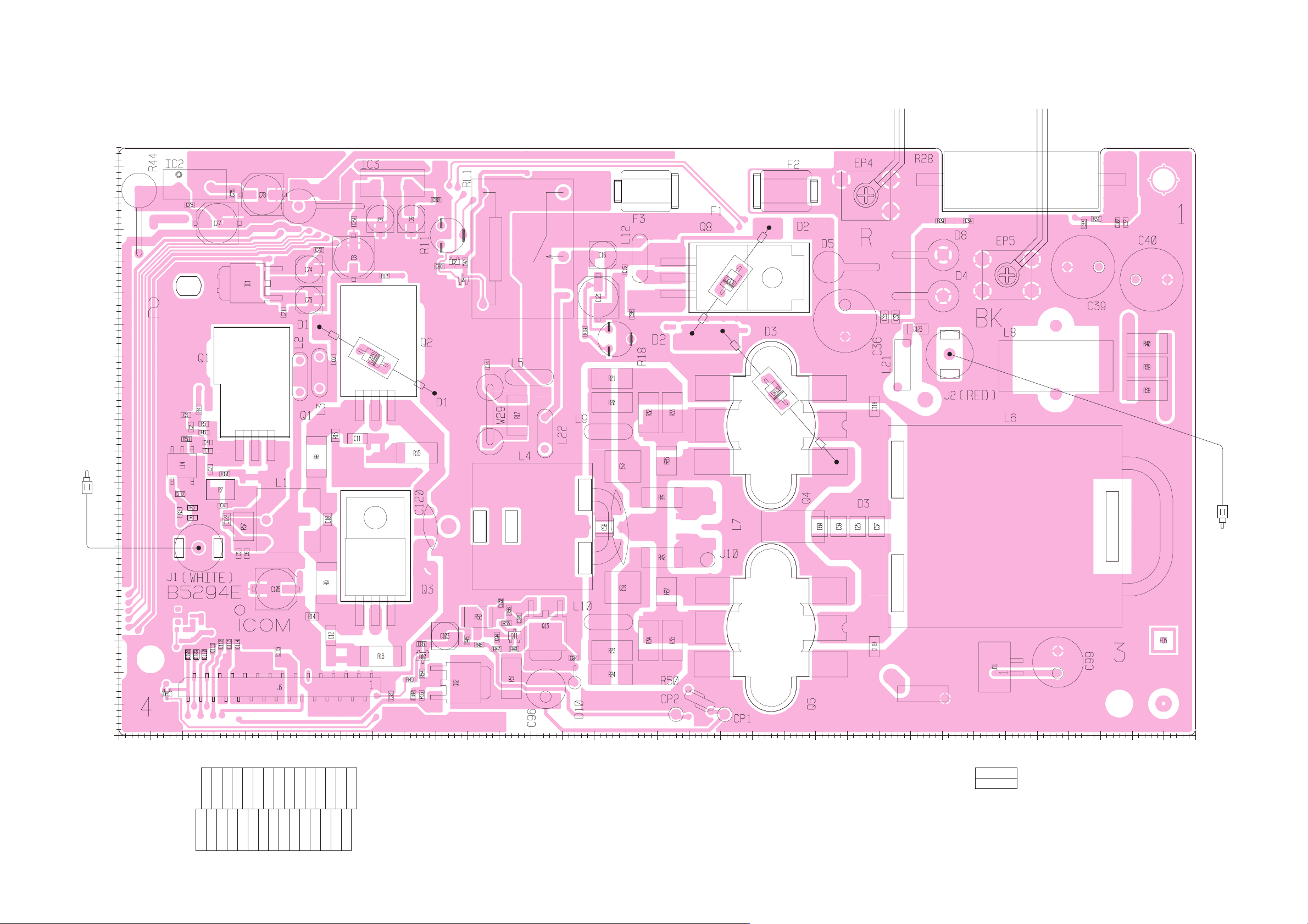
51015 20 25 30 35 40 45 50 55 60 65 70 75 80 85 90 95 100 105 110 115 120 125 130 135 140 145 150 155 160 165 1700
Horizontal
5
10
15
0
25
30
35
20
45
50
55
40
65
70
75
60
80
90
85
Vertical
to FILTER-A unit J1
PAO
P2
to RF-B unit J201
PAI
P1
to FILTER-A unitto FILTER-A unit
PGND
BLACK
PHV
RED
PAT8
30
29
2
1
to MAIN-A unit J771
J3
ICL
H5V
8V
14VA
14V
14V
14V
5V
HV
GND
GND
GND
GND
GND
PWRS
ICH
8V
14VA
14V
14V
14V
14V
5V
NC
GND
GND
GND
GND
GND
MF-2
1
to CHASSIS MF1
J11
MF+
8-16 PA UNIT
• TOP VIEW
8 - 17
Page 91

5101520253035404550556065707580859095100105110115120125130135140145150155160165170 0
Horizontal
5
10
15
0
25
30
35
20
45
50
55
40
65
70
75
60
80
90
85
Vertical
• PA UNIT (BOTTOM VIEW)
8 - 18
Page 92

51015 20 25 30 35 40 45 50 55 60 65 70 75 80 85 90 95 100 105 110 115 120 125 130 135 140 145 150 155 160 165 1700
Horizontal
5
10
15
0
25
30
35
20
45
50
55
40
65
70
75
60
80
90
85
Vertical
BLACK
FGND
FHV
RED
to CHASSIS
W15
to CHASSIS
W15
to PA unit EP5
PGND
BLACK
to PA unit EP4
PHV
RED
PAO
P2
from PA unit J2
CTIN
P1
from CTRL-A unit J1
GND
1
2
9
10
to CTRL-A
unit J13
J3
L8S
L3S
L5S
L2S
GND
L7S
L6S
L1S
L4S
8-17 FILTER-A UNIT
• TOP VIEW
8 - 19
Page 93

5101520253035404550556065707580859095100105110115120125130135140145150155160165170 0
Horizontal
5
10
15
0
25
30
35
20
45
50
55
40
65
70
75
60
80
90
85
Vertical
• FILTER-A UNIT (BOTTOM VIEW)
8 - 20
Page 94

51015 20 25 30 35 40 45 50 55 60 65 70 75 80 85 90 95 100 105 110 115 120 125 130 135 140 145 150 155 160 165 170 175 180 185 1900
Horizontal
5
10
15
0
25
30
35
20
45
50
55
40
65
70
75
60
80
90
95
100
85
Vertical
1
8
5
1
4
14
8
1
7
814
17
41
58
9
16
8
1
41
58
49
64
32
17
116
8
1
9
16
48 33
9
1
10
18
18
169
4
1
5
8
from TUNER-A board J3
P3
TUIN
RFRX
P2
to RF-B
unit J101
CHASSIS
J6
CHASSIS
J5
TUOT
P4
from TUNER-A board J4
CTIN
P1
to FILTER-A unit J2
ANT1 ANT2
GND
22
21
2
1
to TUNER-A
board J5
J8
5M
10M
18M
VHF
GND
14V
CO2
NVHF
CI2
GND
3.5M
7M
14M
24M
GND
14V
CO3
CO1
CI3
CI1
GND
GND
to FILTER-A unit J3
J13
19
102
L8S
L3S
L5S
L2S
GND
L7S
L6S
L1S
L4S
CMCK
to MAIN-A unit J741
J7
2
121
22
FSTB
IKEY
GNDL
ANTS
FORV
-
8V
5V
GND
GND
14V
CMDT
GNDL
ISTA
DRES
REFV
GND
GND
5V
T8V
14V
14V
T14V 1
5
to TUNER
MF2
J11
AW
AX
AY
AZ
T14V 1
5
to TUNER
MF1
J10
PW
PX
PY
PZ
8-18 CTRL-A UNIT
• TOP VIEW
8 - 21
Page 95

5101520253035404550556065707580859095100105110115120125130135140145150155160165170175180185190 0
Horizontal
5
10
15
0
25
30
35
20
45
50
55
40
65
70
75
60
80
90
95
100
85
Vertical
• CTRL-A UNIT (BOTTOM VIEW)
8 - 22
Page 96

51015 20 25 30 35 40 45 50 55 60 65 70 75 80 85 90 95 100 105 110 115 120 125 130 135 140 145 150 155 160 165 170 175 180 185 1900
Horizontal
5
10
15
0
25
30
35
20
45
50
55
40
65
70
75
60
80
90
95
100
85
Vertical
1810
19
1810
19
1
TUIN
P3
to CTRL-A unit J3
TUOT
P4
to CTRL-A unit J4
GND
1
2
21
22
to CTRL-A
unit J8
J5
5M
10M
18M
VHF
GND
14V
CO2
NVHF
CI2
GND
3.5M
7M
14M
24M
GND
14V
CO3
CO1
CI3
CI1
GND
8-19 TUNER-A BOARD
• TOP VIEW
8 - 23
Page 97

5101520253035404550556065707580859095100105110115120125130135140145150155160165170175180185190 0
Horizontal
5
10
15
0
25
30
35
20
45
50
55
40
65
70
75
60
80
90
95
100
85
Vertical
• TUNER-A BOARD (BOTTOM VIEW)
8 - 24
Page 98

9 - 1
SECTION 9 BLOCK DIAGRAM
VOLTAGE LINE
Explanatory notes
TX LINE
RX LINE
COMMON LINE
CLOCK
GENE
IC2041
TC7SHU04FU
IC2042
TC7SH04FU
X2041
CR-568
40MHz
IC2001
ADSP-21061LKS-160
LEVEL
CONV
IC2051
TC74VHC125FT
TIMING
IC2053
TC74HC02AF
IC2054
TC74VHC74FT
LEVEL
CONV
DSP
LEVEL
CONV
IC2072
TC74VHC541FT
ROM
IC2071
SC-1414
LEVEL
CONV
IC2061,IC2063
IC2065,IC2066
TC7SET08FU × 4
CTFL
RTDT
NSQO
DCWK
DSFR
DSDW
DSFW
DSCK
LEVEL
CONV
IC2062
TC74VHC541FT
IC2101
TC7SH32FU
LEVEL
CONV
DSRS
A/D
IC2321
CS5396-KS
VDD
DET
VCC
CTRL
IC2091 S-80934CNMC-G84
IC2092 TC7S02FU
DIFF
CONV
CALS
ACKS
TIMING
IC2341
TC74VHC00FT
IC2343
TC7WH74FU
D/A
IC2351
AD1854JRS
AMP
IC2371A
µPC4570G2
IC2372X
BU4053BCFV
IC2372Y
BU4053BCFV
LPF
IC2401
MAX293CWE
LPF
IC2211B
M5218AFP
MODS
AMS
LPF
IC2291
IC2201X
TC4W53FU
BU4053BCFV
IC2201Y
R2229
AM MOD LEVEL
R2227
FM MOD LEVEL
BU4053BCFV
LIMIT
AMP
IC2211A
M5218AFP
AF
AMP
IC2371B
µPC4570G2
LPF
IF
AMP
AF
AMP
IC2381B
µPC4574G2
LPF
IC2381C,D
µPC4574G2
IC2381A
µPC4574G2
BUFFDIV
IC2342
TC74VHC4040FT
D/A
IC2461
BU9480F
AMP AGC
IC2471B
M5218AFP
BUFF
IC2281A
NJM2058M
IC2441B,C
NJM2058M
LPF
IC2441D
NJM2058M
AF
AMP
EX-SP
JACK
DRIVER
IC3771A TC7W04FU
IC3771B
Q3771 2SA1576
Q3772 2SC4081
D3771 DAN222
EXT-SP SPS
D351
DAN222
Q351
UNR9211J
RL351
AHY103
PWR
AMP
IC332
LA4425A
RIPPLE
FILTER
Q331
2SD1801
14VA
MUTE
IC331
TC4W53FU
AFMS
VCA
AFGV
AAFO
CTXD
CI-V
AF
AMP
IC311
M5282FP
BEEP
ALC
AMP
FMTL
IC372
BA3308F
SQLS
MONV
AF
AMP
IC371
M5282FP
VCA
VCA
BUFF
AF
AMP
AF
AMP
IC451
µPC5023-077
MIGV
AVXL
ATT
PHONE
BOARD
PHONE
JACK
PHNI
MIC
JACK
MIC
BOARD
MUD
PBT
BOARD
PBT1
PBT2
NOTCH
PITCH
TRANSMIT
TRAK
TEN
KEY
TEN-KEY
BOARD
TUNER
TNRD
MONITOR
MOND
DSP-A BOARD
TUNER LED MONITOR LED
NBD
NB
NB LED
NRD
NR
NR LED
KIO
MODE
BOARD
MODE
KEY
KEY
BOARD
KEY
JACK
RIT
BOARD
RIT DIAL
WAVE
FORMER
IC102C,D
MC14071BFEL
-
15V
DC-DC
IC841 NJM2360M
Q841 2SB1124
D841 RB050L-40
IC501 TA79L08F
D501 1SS322
-
7V
REG
IC881 TA79L08F
-
8V
REG
+5V
REG
VRAM
IC3553
LH61665AS-60A
LCD
CONT
X3551
CSTCV26.00MXJ040
26MHz
BUS
DRIVER
IC3551
S1D13504F00A000
IC3501
HD64F2375F20
MAIN
CPU
IC3502
S-80942CNMC-G9C
RTC
BACK UP
SUB
CPU
IC401
HD6433832SD66H
X401
CR-567
3.8304MHz
X3501
CR-520
19.6608MHz
BT3501
CR2032
Q3504 2SA1576
D3504 MA2S111
D3505 MA2S111
D3506 MA2S111
EEPROM
IC3504
RTC-4553A
IC3503
CAT25C32SI
D/A
SERI
PAR A
IC3751
M62352GP
IC3752,IC3753
BU4094BCFV
IC3653,IC3654
TC74AC574FT
BUS
DRIVER
BUS
DRIVER
IC3652
TC74AC245FT
TMDI
TIMER LED
DISPLAY BOARD
8V
R8
REG
Q601
2SD1619
Q602
2SC4081
D601
DA221
RXS
T8
REG
14V
TXS
Q611
2SD1619
Q612
2SC4081
D611
DA221
PAT8
REG
TRVI
Q621
2SA1577
Q622
UMH11N
PAT8
T8V
R8V
-
5V
REG
IC805
AN79L05M
-
5V
POCV
+14V
AMS
PHFS
P5OS
PWR
CTRL
Q501
UMH11N
Q502
UMH4N
REFV
ALC
AMP
ALC
AMP
AMP
FORV
IC571B
NJM4558M
REFL
IC571A
NJM4558M
AMP FORL
ICL
ICH
ALC
AMP
IC551A
NJM2058M
AMP ALCL
ALCEALC
ALC
AMP
IC551D
NJM2058M
Q521
2SA1576
IC201B
BA15532F
IC151
TC4W53FU
IC221
NJM1496V
CERAMIC
BPF
FI111
CFK455E10
(455kHz)
(BW-15kHz)
GATE
CTRL
Q276
2SC4081
Q278
UNR911HJ
D273
MA2S111
NB
DET
D271
1SS375
IF
AMP
BUFF
Q273
2SK882
Q279
2SC4081
AGC
AMP
Q274
2SC4081
Q275
2SA1576
Q272
2SK882
Q271
2SK882
NB
GATE
D113,D114
1SV308 × 2
Q141
3SK131 R8V
T8V T8V
ATT
ATT ATT
MAIN-A UNIT RF-B UNIT
R8V
LO
AMP
ATT
2LO
64.00000MHz
T8V
D1852 HSB88WS
D1752 HSB88WS
LO
AMP
Q2101
2SK882
LPF AMP
PLL UNIT
DPGI
M5V
Q2321 2SJ381
Q2322 2SJ381
5VA
M5V
IC2052
TC7SET08FU
IC2201Z
BU4053BCFV
IC2302
TC4W53FU
IC361
TC4W53FU
(36kHz)
IC551C
NJM2058M
IC551B
NJM2058M
S2LO
77.8MHz
3LO
491kHz
DIFF
CONV
IC2301A
BA15532F
IC2301B
BA15532F
MISL
IC3002X
BU4053BCFV
AFO
VOGV
AF
AMP
IC3003 M5282FP
VCA
IC3005Z
BU4053BCFV
IC3002Z
BU4053BCFV
MOSL
MISL
MOSL
AMPO
IC3005Y
BU4053BCFV
Q471
2SC4081
BUFFAMOD
REC
IC3001
ISD4003-04MS
MOSL
VOSL
HV
AMP
IC3004A
NJM4558M
IC301
RECO
TC4W53FU
MODS
IC2281C,D
NJM2058M
HPF
IC2472A,B
M5218AFP
IC2372Z
BU4053BCFV
IC2473
TC4W53FU
IC2441A
NJM2058M
IC2471A
M5218AFP
AMP
IC2281B
NJM2058M
STON
DMAF
DMAF
AF
AMP
VOXL
MOSL
IC3004B
NJM4558M
IC362
TC4W53FU
-
8V
IC801
BA033T
3.3V
REG
3R3V
IC802
TA7805F
+5V
REG
M5V
Q804
2SD1801
RIPPLE
FIL
D5VA
IC803
MA8051
D801
TA7805F
+5V
REG
BANSBANV
IC101B
NJM4558M
AMP
BPF
FI131
CFWM455D
BPF
FI133
CFWS455IT
IF
AMP
IF
AMP
LO
AMP
LO
AMP
IF
AMP
MODS
DRIV
NBLV
AGC
UNLC
Q241
2SK882
455kHz
ALC
Q261
2SK882
RESETRAMROM
IC1
SC-1415-1
IC2
ID171256SA15PZ
AFL
RFL
BALL
NRL
MIGL
PWRL
CMPL
KYSL
DELL
RF/SQL
AF
BAL
NR
MIC GAIN
RF POWER
COMP
KEY SPEED
BK-IN DELAY
MAIN DIAL
WAVE
FORMER
X4
IC861 TA7805F
-
15V
-
7V
5V
IC821 BA6161F
Q821 2SC4081
D822 RD20M
+18V
DC-DC
14V
-
15V
+18V
POWER
PWRK
LCD
BACK
LIGHT
RGB
CTRL
Q1201,Q1211
Q1221 × 3
2SA1576
CONT
CTRL
IC1521B
M5218AFP
LCD
INTERFACE
IC1401
M52338FP
BKLV
CTRL
Q801 2SC4081
Q802 2SC1201
DC/AC
INVERT
Q803,Q804
2SC3647 × 2
-
8V
+18V
Q901
-
Q903 DTC114EE × 3
Q904 2SC4081
Q905 2SB1201
DIMMER
CTRL
MDM2
MDM1
MDM0
LDV
DSDR
DIV
IC2347
TC74HC390AF
(36kHz)
(491.52kHz)
DTIF
IC3005X
BU4053BCFV
MSL1
MSL2
UT-102
OPTION
SBSY
SSTB
CRXD
DRIF
DTAF
BUFF
IC2353
TC7SH04FU
DSIR
X2351
CR-643
24.576MHz
IC2352
TC7SHU04FU
36kHz
RX TOT AL GAIN
R210
IC201A
BA15532F
IC153
TC4SU69F
IC152
TC4SU69F
LPF
DTAF
MEMORY BOARD
IC3651
IC3656 TC74AC32FT
IC3655 TC74AC08FT
TC74AC244FT
CNTV
BKLV
455kHz
64.455MHz
DRIVER
Q1901
XP4311
14V
R8V
Q1801
2SK882
Q904
2SC2714
COMMON LINE
RX LINE
TX LINE
DATA BUS LINE
DRAF
MICI
IC101B,C,D
BU4030BF
IC102A
MC14071BFEL
IC101A
BU4030BF
IC102B
MC14071BFEL
PB1A
PB1B
PB2A
PB2B
NOTL
PITL
IF
AMP
IF
AMP
IF
AMP
A
B
C
D
E
F
G
H
Page 99

9 - 2
VOLTAGE LINE
Explanatory notes
TX LINE
RX LINE
COMMON LINE
IF
AMP
Q1751
3SK131
AGC
XTAL
BPF
FI1701
FL
-
381
(64.455MHz)
(BW=15kHz)
T8V
COMB
IF
AMP
Q1208
2SC5551
PIN
ATT
D1201 CPH5513
D1203 1SV263
D1204 CPH5513
Q1207
2SC4081
DRIVER
IF
AMP
AMP
Q1008
2SC5551
Q1209
MMBFU310
PIN
ATT
D1001 CPH5513
D1002 1SV263
D1003 CPH5513
Q1007
2SC4081
DRIVER
Q1203
-
Q1206
2SK1740
Q1551
2SK882
IF
AMP
ALC
T8V
R8V
D2201
1SV263
PIN
ATT
IF
AMP
Q2202
2SK882
IF
AMP
Q2201
2SK882
D2101
HSB88WS
CERAMIC
BPF
FI2003
SFECV13.35MAS
AGC
ATT
ATT
DET
IC2001 TA31136FN
CERAMIC
BPF
FI2001
CFJ455K8
AGC
AMP
D2002
MA2S111
IC2002B
NJM4558M
AMP
IC2002A
NJM4558M
SCPL
DRIVER
Q2203
2SC4081
SATV
Q1003
-
Q1006
2SK1740
AMP
RF
Q1201,Q1202
2SK1740
LPF
SPLIT
DRIVER
Q4203,Q4204
XP4311
AMP
RF
Q1001,Q1002
2SK1740
LPF
DRIVER
Q4301,Q4303
XP4311
A
B
Q4201
2SC5551
Q4202
2SC5551
PRE
AMP
Q4302
2SC5551
PRE
AMP
PRE2
T8V
ATT
PRE1
14V
LPF
BPF
BOARD
PREAMP BOARD
ATT
BPF
BPF
BPF
BPF
BPF
BPF
BPF
BPF
BPF
HPF
BPF
1.6
-
2.0MHz
HPF
B1
2.0
-
3.0MHz
B2
3.0
-
4.0MHz
B3
4.0
-
6.0MHz
B4
6.0
-
8.0MHz
B5
8.0
-
11.0MHz
B6
11.0
-
15.0MHz
B7
15.0
-
22.0MHz
B8
22.0
-
30.0MHz
B9
50.0
-
54.0MHz
B10
30
-
50MHz
54
-
60MHz
B10W
BPF
50.0-54.0MHz
TX-B10
D1451
HSB88WS
LPF
Q1301
2SC5551
LO
AMP
LPF
Q1101
2SC5551
LO
AMP
POFF
B0
ATT
12dB
RL103
ATN203
ATT2
ATT
6dB
ATT1
RL102
ATN203
RANS
LPF
ATT
YGR
AMP
IC201
µPC1678GV
LPF ATT
RX ANT
RF-B UNIT
D151
1SV307
MUTE
MUTE
CTRL
Q152 UNR9211J
Q151 UMH11N
Q201 2SA1576
Q202 UMH11N
Q203 UNR9211J
TRVI
T8V
ANT2 ANT1
CHASSIS
ANTS
CURRENT
DET
TUNING
NET
TUNER
ON/OFF
CTRL
TUNER-A UNIT
TX/RX
CONRT
THRU
LPF
RESIST
DET
PHASE
DET
SWR
DET
CPU
DATA
X1 CR-569
6.144MHz
IC5
M38022M2-138FP
IC13
TA7805F
+5
REG
14V 5V
FOR
REF
CTRL-A UNIT
X2
Q71 2SC4081
Q81 2SC4405
Q801
2SC4081
AMPDDS
IC801
SC-1287
PST7
D/ABPF
Q802
2SC4117
BUFF
HPF
PLL
IC
PST6
LOOP
FIL
77.8MHz
BUFF
PSMT
Q701
2SC4081
AMP
PST5
DDSBPF D/A
IC701
SC-1287
VCO-B
Q521 2SK508
D521 KV1770S
D522 KV1770S
Q501 2SK508
D501 KV1770S
D502 KV1770S
Q551 2SK508
D551
-
D554
MA338 × 4
Q571 2SK508
D571
-
D574
MA338 × 4
BUFF
DATA
PLL
IC
LOOP
FIL
PST4
BPF
CTRL
Q651
DTA114EE
BPF MUTE
DRIVER
Q424
UMD3N
BUFF
Q452
2SC4081
IC681
LMX2306TM
LOOP
FIL
D451
MA357
Q451
2SK210
Q402
2SC4081
AMP
PHASE
DET
AMP
IC402
TC7S04F
CERAMIC
BPF
D/A
FI401
CFEC10,8MD11
DDS
DRIVER
Q421,422,423,426
UMD3N
1/4
DDS
VB1S
VB2S
VB3S
VB4S
Q403
2SC4081
AMP
Q52
2SC4081
BUFF
X52
CR-338.
32.00056MHz
CAL PST2
VCO-A
D202 KV1770S
Q201 2SK508
D201 KV1770S
Q221 2SK508
D221,D222 KV1770S × 2
BUFF
Q601
2SC4403
Q301
2SC4403
D/A
AMP
Q151
2SK210
D151
MA357
LOOP
FIL
Q102
2SC4081
IC381
LMX2306TM
Q152
2SC4081
BUFF
Q124
UMD3N
DRIVER
DATA
PLL
IC
LOOP
FIL
PST2
Q351
DTA114EE
BPF
CTRL
BPF MUTE
Q121-Q123 UMD3N
Q126 UMD3N
DRIVER
FI101
CFEC10,8MD11
DDS
CERAMIC
BPF
PHASE
DET
IC102
TC7S04F
AMP
DDS
VA1S
VA2S
VA3S
VA4S
Q103
2SC4081
AMP
MKRS
MUTE
IC191
TC7S08F
DULS
PST1
LEVEL
CONV
UNLC
CON0
CON1
CON2
IC1
BU4094BCF
SERI
PARA
PSEL
PSTB
PST1
PST2
PST3
PST4
PST5
PST6
PST7
1.8MHz
LPF
3.5MHz
LPF
5/7MHz
LPF
10MHz
LPF
14MHz
LPF
18/21MHz
LPF
24/28MHz
LPF
50MHz
LPF
L1S
L2S
L3S
L4S
L5S
L6S
L7S
L8S
PWR
AMP
Q4
2SC5125
Q5
2SC5125
BIAS
Q8
2SD1585K
BIAS
DRIVE
AMP
Q2
2SC1972
Q3
2SC1972
Q1
2SC1971
PRE
DRIVE
COMMON
FILTER
13.8V
Q10 2SC4081
Q11 2SC4081
Q12 2SB1201
Q13 2SB1201
FAN
CTRL
FUSE
(5A)
RELAY
CTRL
Q9 UNR9211J
D7 DAP222
+5
REG
IC2
TA7805S
+5
REG
IC1
TA7805F
+8
REG
IC3
MC78T08C
HV
H5V
14V
5V
8V
FILTER-A UNITPA UNIT
0.03-1.6MHz
RL101
ATN203
Q101
UNR9211J
XVRT
Q51
2SC4403
Q2 UMD3N
MKRS
1LOA
1LOB
64.455MHz
BLAV
D1205
MA2S111
D1004
MA2S111
BLBV
8V
LPF
T8V
64.455MHz
FI2002
SFECV13.35MAS
CERAMIC
BPF
SAGC
64.485MHz-124.455MHz
RF
AMP
IC1401
µPC2708TB
LPF
B0-B10
B10W
TX-B10
POFF
PRE1
PRE2
RANS
ATT1
ATT2
DRIVER
SERI
PAR A
IC301,IC302
TD62783AF × 2
Q351,Q352
UMH11N × 2
Q353
-
Q357
XP4311 × 5
D301
-
D303,D351,D352
DAN222 × 5
IC401,IC402,IC403
CD4094BPWR × 3
MCK
MDAT
BSTB
S3LO 12.79
-
12.99MHz
PSMT
Q903
2SC4117
IC901
LC7153M
IC902
TC7W08F
SW
Q902
2SK508
DATA
PBMT
PBFS
IC401
SC-1246A
LPF
+5
REG
IC682 TA78L05F
8V 5V PLLB
Q661
DTC114EE
8MHz
VCO
SW
Q522 2SC4213
Q502 2SC4213
VCO
SW
Q552 2SC4213
VCO
SW
Q572 2SC4213
VCO
SW
Q202 2SC4213
VCO
SW
Q251 2SK508
D251
-
D254 MA338 × 4
Q271 2SK508
D271-D274 MA338 × 4
VCO
SW
Q222 2SC4213
Q252 2SC4213
VCO
SW
Q272 2SC4213
VCO
SW
Q361
DTC114EE
IC101
SC-1246A
PAFS
PAM T
64.485MHz-124.455MHz
+5
REG
IC382 TA78L05F
5V PLLA8V
CTIN
D15
HSM88AS
Q14,Q16 DTC114EU × 2
Q13,Q17 DTA114EU × 2
Q12 DTC114EU
Q13 DTA114EU
RX
D8,D9
HSM88AS × 2
D4
DWA010
D1,D2
HSM88AS × 2
PAI
A
B
C
D
E
F
G
H
Page 100

SECTION 10 VOLTAGE DIAGRAMS
VOLTAGE LINE
Explanatory notes
44
45
43
42
41
40
39
38
37
36
35
34
33
32
3130292827
26
61
62
63
64
65
66
67
68
69
70
71
72
73
74
75
82818384858687888990919293949596979899
100
15
13
12
11
10
9
8
7
6
5
4
3
2
1
P81/SEG26
P82/SEG27
P83/SEG28
P84/SEG29
P85/SEG30
P86/SEG31
P87/SEG32
P90/SEG33
P91/SEG34
P92/SEG35
P93/SEG36
P94/SEG37/M
P95/SEG38/D0
P96/SEG39/CL2
P97/SEG40/CL1
P15/IRQ1/TMIB
P14/PWM
P16/TRQ2/TMIC
P17/IRQ3/TMIF
P40/SCK3
P41/RXD
P42/TXD
P43/IRQ0
AVCC
PB0/AN0
PB1/AN1
PB2/AN2
PB3/AN3
PB4/AN4
PB5/AN5
PB6/AN6
PB7/AN7
PC0/AN8
PC1/AN9
PC2/AN10P37/CS
PC3/AN11
AVSS
TEST
X2
X1
VSS
OSC1
OSC2
RES
MDO
P20/IRQ4/ADTRG
P21/UD
P22
P23
P24
VSSV3V2V1VCC
PA3/COM4
PA2/COM3
PA1/COM2
PA0/COM1
P50/WKP0/SEG1
P51/WKP1/SEG2
P52/WKP2/SEG3
P53/WKP3/SEG4
P54/WKP4/SEG5
P55/WKP5/SEG6
P56/WKP6/SEG7
P57/WKP7/SEG8
P60/SEG9
P61/SEG10
46 80
P13/TMIGP62/SEG11
P63/SEG12 P12/TMOFH
79 47
48 78
P11/TMOFLP64/SEG13
P65/SEG14 P10/TMOW
77 49
60 16
P80/SEG25P25
P66/SEG15 VCC
76 50
59 17
P77/SEG24P26
58 18
P76/SEG23P27
57 19
P75/SEG22P30/SCK1
56 20
P74/SEG21P31/SI1
55 21
P73/SEG20P32/SO1
54 22
P72/SEG19P33/SCK2
53 23
P71/SEG18P34/SI2
52 24
P70/SEG17P35/SO2
51 25
P67/SEG16P36/STRB
14
IC401
HD6433832SD66H
5VF
C401
12p
C402
12p
R401
1M
X401
CR-567
11
10
9
12
13
14
15
16
7
6
8
5
4
3
2
1
IC411
BU4051BCFV
X4 VDD
X6
X
X7
X5
INH
VEE
VSS
X2
X1
X0
X3
A
B
C
C411
0.1
SPLK
5VF
R404 47k
R405 47k
R406 47k
R407 47k
MIGL
PWRL
CMPL
KYSL
DELL
5VF
RFL
AFL
NRL
BALL
UP
E
DN
RDN
5VF
RUP
5VF
RDN
RUP
J120
J1
RIT BOARD
S1
EVQ-VCJF0324B
5VF
J101
F4K
F3K
F5K
J201
J1
R201 1k
R202 1k
R203 1k
R204 1k
R205 1k
R206 1k
R207 1k
R208 1k
R209 1k
R210 1k
R211 1k
F5K
F4K
F3K
F2K
F1K
SPEK
EXTK
FILK
AMK
CWK
SSBK
KI2
KI1
5VF
R215
47k
R214 47k
R213 47k
R212 47k
F2K
F1K
SPEK
EXTK
FILK
AMK
CWK
SSBK
KI2
KI1
5VF
R224 1k
R227 1k
R226 1k
R225 1k
R230 1k
R229 1k
R228 1k
R223 1k
J221
R222 1k
R221 1k
R231 1k
14K
10K
7K
3K
SPLK
1K
18K
21K
24K
28K
50K
R232 1k
GENK
R233 1k
FINK
R234 1k
MPWK
R235 1k
MPRK
R244 1k
R247 1k
R246 1k
R245 1k
R251 1k
R250 1k
R249 1k
R248 1k
R243 1k
J241
R242 1k
R241 1k
XFCK
TSK
MCLK
MWK
MUPK
MDNK
LOCK
PBTK
NOTK
KI4
5VF
KI3
LDV
R252 1k LOCD
R253 1k TXD
R254 1k RXD
R255 1k NOTD
PBTD
S5
(F-5)
S4
(F-4)
S3
(F-3)
S2
(F-2)
S1
(F-1)
S10
(EXIT)
S9
(FILTER)
S8
(AM/FM)
S7
(CW/RTTY)
S6
(SSB)
S11
(SPEECH)
S17
(F)
S15
(D)
S14
(C)
S13
(B)
S12
(A)
S18
(G)
S16
(E)
R1
6.8k
R5
6.8k
R2
2.2kR34.7k
R4
15k
R6
2.2k
R7
4.7k
C2 0.1
C1
0.1
MODE BOARD
DISPLAY BOARD
J1
J2
S24
(PBT-CL)
PBTK
S25
(NOTCH)
NOTK
S26
(RIT)
S27
( TX)
S28
(CLEAR)
KI4
C2
0.1
R5
6.8k
R6
2.2k
R7
4.7k
S18
(UP)
MUPK
S19
(DOWN)
MDNK
S20
(MW)
MWK
S21
(M-CL)
MCLK
S22
(TS)
TSK
S23
(XFC)
XFCK
S14
(7)
7K
S15
(18)
18K
S16
(28)
28K
S17
(F-INP)
FINK
S30
(MP-R)
MPRK
S31
(LOCK)
LOCK
S10
(3.5)
3K
S11
(14)
14K
S12
(24)
24K
S13
(50)
50K
S6
(1.8)
1K
S7
(10)
10K
S8
(21)
21K
S9
(GENE)
GENK
S29
(MP-W)
MPWK
S1
(SPLIT)
SPLK
S2
(DW)
S3
(CHANGE)
S4
(V/M)
S5
(M/S)
C1
0.1
R2
2.2k
R3
4.7k
R4
15k
R1
6.8k
TEN-KEY BOARD
Q1
DTC114EE R8
5.6k
DS1
CL-200HR
(LOCK) LED
Q2
DTC114EE R9
5.6k
DS2
CL-200HR
(TX) LED
Q3
DTC114EE R10
680
DS3
CL-220YG
(RX) LED
Q4
DTC114EE R11
1k
DS4
CL-220YG
(NOTCH) LED
Q5
DTC114EE R12
1k
DS5
CL-220YG
(TWIN PEAK FILTER) LED
J801
1
14
7
3
2
10
9
8
R102
15k
C102
0.001
5
C104
0.001
R104
47k
6
4
C103
0.001
R103
15k
11
13
12
4
6
5
3
14
7
2
1
IC101c
BU4030BF
IC101b
BU4030BF
IC101d
BU4030BF
IC102b
MC14071BFEL
IC102a
MC14071BFEL
IC101a
BU4030BF
IC102d
MC14071BFEL
12
11
13
R126
220k
R127
100k
R128 1M
C122
0.001
R125
100k
C121
0.001
R121
100k
R124 1M
5VF
R123
100k
R122
220k
9
10
8
IC102c
MC14071BFEL
RSB
RSA
8
7
6
54
3
2
1
CDCS
ES
CT
GND
SI
V+
INVIN
C848
0.1
C847
220
L843
D10F-A814AY-101K
D841
RB050L-40
C843
330p
L842
SLF12565T-680M2R0
C844
220
C845
0.1
R845
1.2k
R847
27k
R846
27k
C842
0.1
C841 220
IC841
NJM2360AM
C805
15p
C804
0.047
R805
3.3k
R804
3.3k
L802
D10F-A814AY-101K
D801
RD3.0M
R801
33k
C801
10
C80347R803
220
R806
47k
L803
D818HN-1107
C802
10
L801
100µH
R802
33k
Q802
2SB1201
Q801
2SC4081
5VF
Q804
2SC3647
Q803
2SC3647
C101
0.1
14K
10K
7K
3K
SPLK
1K
18K
21K
24K
28K
50K
GENK
FINK
MPWK
MPRK
XFCK
TSK
MCLK
MWK
MUPK
MDNK
LOCK
PBTK
NOTK
KI4
5VF
KI3
LDV
LOCD
TXD
RXD
NOTD
PBTD
FRONT
W4
FRONT
W6
FRONT
W7
FRONT
W8
to
LCD
MUP
MDN
GND
J802
to
LCD
Q805
DTC114EE
W801
R256 1k
C242
0.1
C241
0.1
R101
100
R105
100
C105
0.1
KI4
KI3
R447
100
KI0
D421
DAN222
D423
DAN222
D422
DAN222
R431
2.2k
R4211kR424
1k
D425
DAN222
D424
DAN222
D431
DAN222
D432
DAN222
R432 47k
C431 0.1
R403
100k
R402
1k
SRES
DASH
DOT
DOTK
DSHK
MUD
+14V
BKLV
C846 220
L841
D10F-A814AY-101K
R841
0.33
R842
0.33
-
15V
+18V
+14V
5VF
C823
0.0047
C828
10
C826
4.7
C830
10
D822
RD20M
C829
4.7
C825
0.0047
C827
4.7
C824
0.0047
C82247C821
0.1
Q821
2SC4081
R824
10k
L823
1000µH
R821
1.2k
IC821
BA6161F
D821 1SS322
L822
NLFC565050T-472K
L821
HF50ACC322413-B
8
7
6
5
1
2
3
4
F1K
ASL1
MSB
ASL0
F2K
F3K
F4K
F5K
SSBK
CWK
AMK
FILK
EXTK
SPEK
ASL2
PITL
NOTL
DELL
KYSL
CMPL
PWRL
MIGL
NRL
BALL
RFL
AFL
PB2B
LFMD
LMFD
PB2A
RSB
MSA
RSA
PB1B
BKLV
CNTV
PB1A
METV
MSA
R446 10k
R445 10k
R444 10k
R443 47k
R442 47k
R441 10k
L401
HF50ACC322513-B
C404
0.1
C405
0.1
C406
10
1K3K7K
10K
14K
18K
21K
24K
28K
50K
GENK
FINK
MPWK
MPRK
MUPK
MDNK
MWK
MCLK
TSK
NOTD
PBTD
RXD
TXD
LOCD
NRD
NBD
MOND
TNRD
MDM2
MDM1
MDN0
BKLS
HDD2
HDD1
HDD0
MAT1
PHNI
DSHK
DOTK
TRAK
NOTK
PBTK
LOCK
XFCK
R416 47k
R415 47k
R414 47k
R413 47k
R412 47k
R411 47k
R410 47k
R409 47k
R408 47k
C403
0.1
R861
12
R862
12
R863
12
C861 10
C862 0.1
C863 0.1
C864 22
IO
G
IC861
TA7805F
CP400
OI
R882
56
R881
56
C881 10
C882 0.1
C883 0.1
-
8V
C884 22
G
IC881
TA79LO8F
OI
C501 10
C502 0.1
C503 0.1
C504 22
G
IC501
TA79LO8F
D501
1SS322
COGC
(COMMON GAIN)
(CLAMP CONTROL)
CPCN
D509 1SS322
+4R5V
-
7R5V
R1101
47k
KIO
+14V
GND
GND
GND
GND
GND
GND
GND
R107
220k
R106
220k
GND
GND
GND
GND
GND
GND
GND
GND
GND
CP101
CP102 CP103
CP104
MUDK
(INPUT SELECT)
R1112
33k
R1113
27k
R1121
27k
R1122
4.7k
CNTV
CFL+
CFL
-
R807
27
R808
27
C849 220
C850 220
R850 330
Q841
2SB1124S
R848 470
R849 470
AS0
–8V
+14V
CNTV
5VF
A
B
C
D
E
F
G
H
I
J
K
L
M
N
O
P
Q
R
S
T
U
V
W
X
Y
Z
AA
AB
AC
AD
AE
AF
AG
AH
AI
-
18V
+14V
-
15V
4.8V
4.8V
RSB
RSA
RIT DIAL UP RIT DIAL DOWN
4.6V
MAIN DIAL DOWNMAIN DIAL UP
4.6V
M UP
M DN
OFF 4.8V
A 0V
B 1.2V
C 2.4V
D 3.7V
OFF 4.8V
E 0V
F 1.2V
G 2.4V
OFF 4.8V
RIT 0V
∆TX 1.2V
CLEAR 2.4V
OFF 4.8V
DUAL WATCH 0V
CHANGE 1.2V
VFO/MEMO 2.4V
MAIN/SUB 3.7V
ON 4.5V
OFF 0V
ON 4.5V
OFF 0V
LCD BACKLIGHT
MAX 4.8V
MIN 0V
-
15.4V
18.6V
1.5V
0.1µS
4.8V
1.3V
1.6V
10-1 FRONT UNIT
10 - 1
 Loading...