

Page 1
SERVICE
MANUAL
PMR446 FM TRANSCEIVER
Page 2
INTRODUCTION
6-9-16, Kamihigashi, Hirano-ku, Osaka 547-0002, Japan
Phone : 06 6793 5302
Fax : 06 6793 0013
Communication Equipment
Himmelgeister Str. 100, D-40225 Düsseldorf, Germany
Phone: 0211 346047 Fax : 0211 333639
URL : http://www.icomeurope.com
Unit 9, Sea St., Herne Bay, Kent, CT6 8LD, U.K.
Phone: 01227 741741 Fax : 01227 741742
URL : http://www.icomuk.co.uk
Zac de la Plaine, Rue Brindejonc des Moulinais
BP 5804, 31505 Toulouse Cedex, France
Phone: 561 36 03 03 Fax : 561 36 03 00
URL : http://www.icom-france.com
Crta. de Gracia a Manresa Km. 14,750
08190 Sant Cugat del Valles Barcelona, SPAIN
Phone: (93) 590 26 70 Fax : (93) 589 04 46
URL : http://www.icomspain.com
<
Corporate Headquarters
>
2380 116th Avenue N.E., Bellevue, WA 98004, U.S.A.
Phone: (425) 454-8155 Fax : (425) 454-1509
URL : http://www.icomamerica.com
<
Customer Service
>
Phone: (425) 454-7619
A.C.N. 006 092 575
290-294 Albert Street, Brunswick, Victoria, 3056, Australia
Phone: 03 9387 0666 Fax : 03 9387 0022
URL : http://www.icom.net.au
6F No. 68, Sec. 1 Cheng-Teh Road, Taipei, Taiwan, R.O.C.
Phone: (02) 2559 1899 Fax : (02) 2559 1874
3071 #5 Road, Unit 9, Richmond, B.C., V6X 2T4, Canada
Phone: (604) 273-7400 Fax : (604) 273-1900
URL : http://www.icomcanada.com
This service manual describes the latest service information
for the
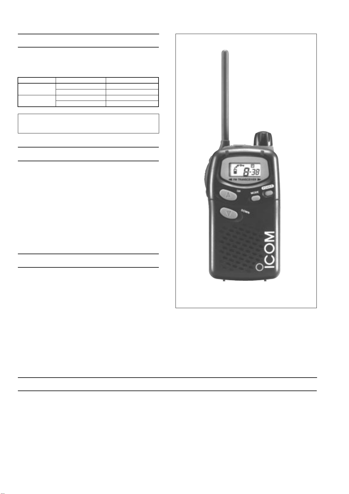
IC-446S PMR446 FM TRANSCEIVER
publication.
at the time of
VERSION SYMBOL
Europe
General
EUR
EUR-1
GEN
GEN-1
BODY COLOR
BLACK
YELLOW
BLACK
YELLOW
To upgrade quality, all electrical or mechanical parts and
internal circuits are subject to change without notice or obligation.
DANGER
NEVER connect the transceiver to an AC outlet or to a DC
power supply that uses more than 5 V. Such a connection
could cause a fire hazard and/or electric shock.
DO NOT expose the transceiver to rain, snow or any liquids.
DO NOT reverse the polarities of the power supply when
connecting the transceiver.
DO NOT apply an RF signal of more than 20 dBm (100mW)
to the antenna connector. This could damage the transceiver's front end.
ORDERING PARTS
Be sure to include the following four points when ordering
replacement parts:
1. 10-digit order numbers
2. Component part number and name
3. Equipment model name and unit name
4. Quantity required
<SAMPLE ORDER>
1110002820 S.IC NJM2100M IC-446S MAIN UNIT 5 pieces
8810009560 Screw PH BO M2x6 ZK IC-446S Chassis 10 pieces
Addresses are provided on the inside back cover for your
convenience.
1. Make sure a problem is internal before disassembling the transceiver.
2. DO NOT open the transceiver until the transceiver is disconnected from its power source.
3. DO NOT force any of the variable components. Turn them slowly and smoothly.
4. DO NOT short any circuits or electronic parts. An insulated turning tool MUST be used for all adjustments.
5. DO NOT keep power ON for a long time when the transceiver is defective.
6. DO NOT transmit power into a signal generator or a sweep generator.
7. ALWAYS connect a 30 dB or 40 dB attenuator between the transceiver and a deviation meter or spectrum analyzer when
8. READ the instructions of test equipment thoroughly before connecting equipment to the transceiver.
using such test equipment.
REPAIR NOTES
Page 3

TABLE OF CONTENTS
SECTION 1 SPECIFICATIONS
SECTION 2 INSIDE VIEWS
SECTION 3 DISASEMBLY INSTRUCTION
SECTION 4 CIRCUIT DESCRIPTION
4-1 RECEIVER CIRCUITS . . . . . . . . . . . . . . . . . . . . . . . . . . . . . . . . . . . . . . . . . . . . . . . . . . . . .4-1
4-2 TRANSMITER CIRCUITS . . . . . . . . . . . . . . . . . . . . . . . . . . . . . . . . . . . . . . . . . . . . . . . . . .4-2
4-3 PLL CIRCUITS . . . . . . . . . . . . . . . . . . . . . . . . . . . . . . . . . . . . . . . . . . . . . . . . . . . . . . . . . . .4-2
4-4 POWER SUPPLY CIRCUITS . . . . . . . . . . . . . . . . . . . . . . . . . . . . . . . . . . . . . . . . . . . . . . . .4-3
4-5 PORT ALLOCATIONS . . . . . . . . . . . . . . . . . . . . . . . . . . . . . . . . . . . . . . . . . . . . . . . . . . . . .4-3
SECTION 5 ADJUSTMENT PROCEDURES
5-1 PREPARATION . . . . . . . . . . . . . . . . . . . . . . . . . . . . . . . . . . . . . . . . . . . . . . . . . . . . . . . . . .5-1
5-2 PLL AND TRANSMITTER ADJUSTMENTS . . . . . . . . . . . . . . . . . . . . . . . . . . . . . . . . . . . . .5-2
5-3 RECEIVER ADJUSTMENT . . . . . . . . . . . . . . . . . . . . . . . . . . . . . . . . . . . . . . . . . . . . . . . . . .5-3
SECTION 6 PARTS LIST
SECTION 7 MECHANICAL PARTS AND DISASSEMBLY
SECTION 8 SEMI-CONDUCTOR INFORMATION
SECTION 9 BOARD LAYOUTS
9-1 MAIN UNIT . . . . . . . . . . . . . . . . . . . . . . . . . . . . . . . . . . . . . . . . . . . . . . . . . . . . . . . . . . . . .9-1
9-2 RF UNIT . . . . . . . . . . . . . . . . . . . . . . . . . . . . . . . . . . . . . . . . . . . . . . . . . . . . . . . . . . . . . . .9-3
SECTION 10 BLOCK DIAGRAM
SECTION 11 VOLTAGE DIAGRAM
11-1 MAIN UNIT . . . . . . . . . . . . . . . . . . . . . . . . . . . . . . . . . . . . . . . . . . . . . . . . . . . . . . . . . . . . .11-1
11-2 RF UNIT . . . . . . . . . . . . . . . . . . . . . . . . . . . . . . . . . . . . . . . . . . . . . . . . . . . . . . . . . . . . . . .11-2
Page 4
All stated specifications are subject to change without notice or obligation.
‘‘
GENERAL
Number of channels : 8 ch
Type of emission : 8K50F3E
Frequency stability : ±2.5 kHz
Frequency resolution : 12.5 kHz
Power supply requirements : 3
× AA(R6) dry, alkaline;
(negative ground) or optional BP-202
Current drain : Less than 500 mA
Operating temperature range : –20˚C to +55˚C
Number of CTCSS frequency: 38 (67.0–250.3 Hz)
Dimensions (mm) : 55.5(W)
×102.5(H)×26.5(D)
(proj. not included)
Weight (included 3 cells) : 180 g
‘‘
TRNSMITTER
Output power : 500 mW
Modulation system : Variable reactance
frequency modulation
Max. freqequency deviation : ±2.5 kHz
Spurious emissions : Less than 0.25 µW
Adjacent channel power : More than 60 dB
External mic.connector : 3-conductor
2.5(d) mm/2.2 kΩ
‘‘
RECEIVER
Receiving system : Double conversion
superheterodyne
Intermediate frequency : 1st 21.7 MHz
2nd 450 kHz
Sensitivity (12 dB SINAD) :
Less than 0.25 µV; –12 dBµV
Adjcent chnnel selectivity : 55 dB
Spurious response : 65 dB
Intermoduration : 60 dB
Audio output power : 100 mW at 10% distortion
(at 4.5 V DC) with an 8 Ω load
External SP connector : 2-conductor
3.5 (d) mm (
1
⁄8")/8 Ω
‘‘
CHANNEL FREQUENCY LIST
‘‘
CTCSS FREQUENCY LIST
SECTION 1 SPECIFICATIONS
1 - 1
Channel Frequency Channel Frequency
No. (MHz) No. (MHz)
1
2
3
4
446.00625
446.01875
446.03125
446.04375
5
6
7
8
446.05625
446.06875
446.08125
446.09375
Channel Frequency Channel Frequency
No. (Hz) No. (Hz)
1
2
3
4
5
6
7
8
9
10
11
12
13
14
15
16
17
18
19
20
67.0
71.9
74.4
77.0
79.7
82.5
85.4
88.5
91.5
94.8
97.4
100.0
103.5
107.2
110.9
114.8
118.8
123.0
127.3
131.8
21
22
23
24
25
26
27
28
29
30
31
32
33
34
35
36
37
38
---
136.5
141.3
146.2
151.4
156.7
162.2
167.9
173.8
179.9
186.2
192.8
203.5
210.7
218.1
225.7
233.6
241.8
250.3
OFF
Page 5
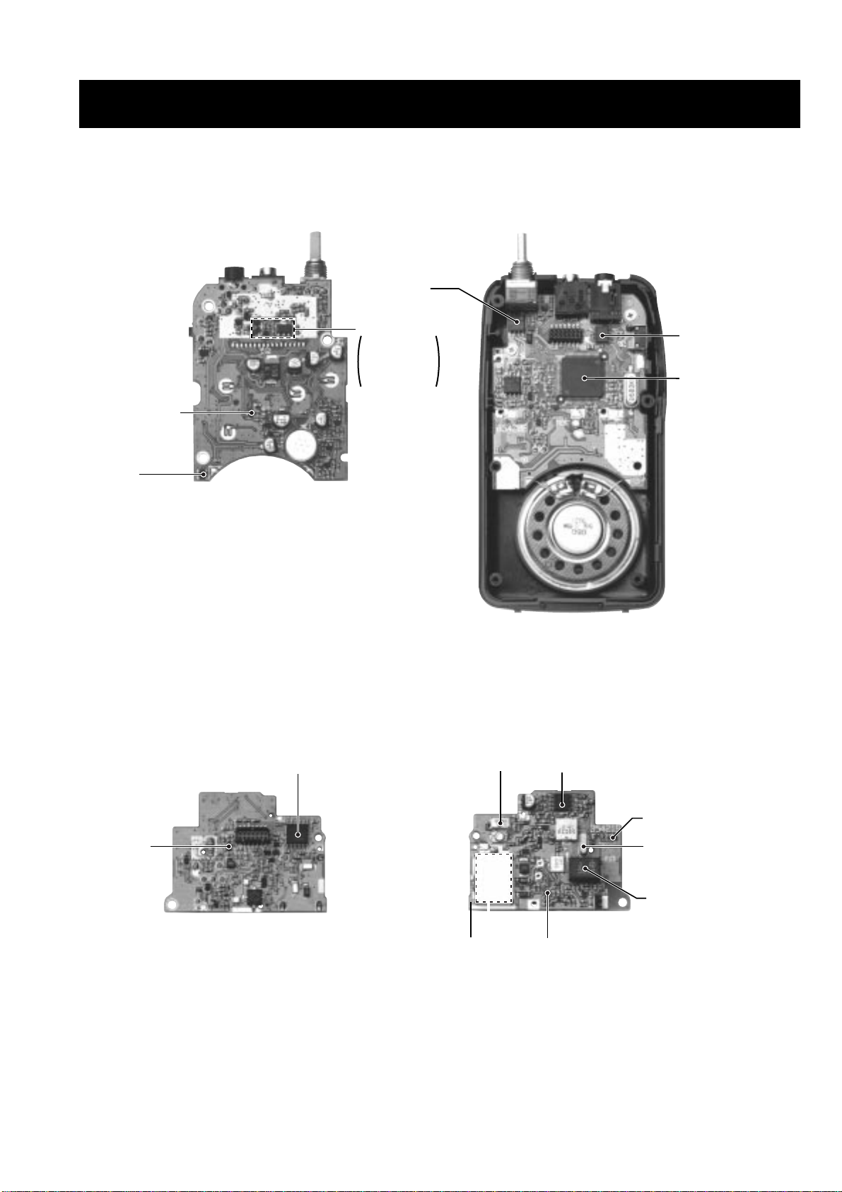
SECTION 2 INSIDE VIEWS
•
MAIN UNIT
2 - 1
•
RF UNIT
T+3 Current amplifier
Q27: 2SC4081
Q28: 2SB798
Q101: UMZ1N
D5: 1SS355
R+3 Current amplifier
(Q18: 2SA1586)
AF amplifier
(IC9: NJM2070M)
EEPROM
(IC3: AT24C02N)
CPU
(IC1: µPD753036GK)
+3 Regurator
(IC6: S-81230SG)
TOP VIEW BOTT OM VIEW
1st mixer
(Q2: 3SK284)
Reference oscilletor
(X1: CR-669 21.25MHz)
PLL IC
(IC1: µPD3140GS)
TOP VIEW BOTT OM VIEW
VCO circuit
FM IF IC
(IC2: TA31136FN)
1st IF filter
(FI2: FL-297)
1st IF amplifier
(Q1: 2SC4215)
2nd IF filter
(FI3: CFWN450G)
RF amplifier
(Q3: 2SC4226)
Page 6
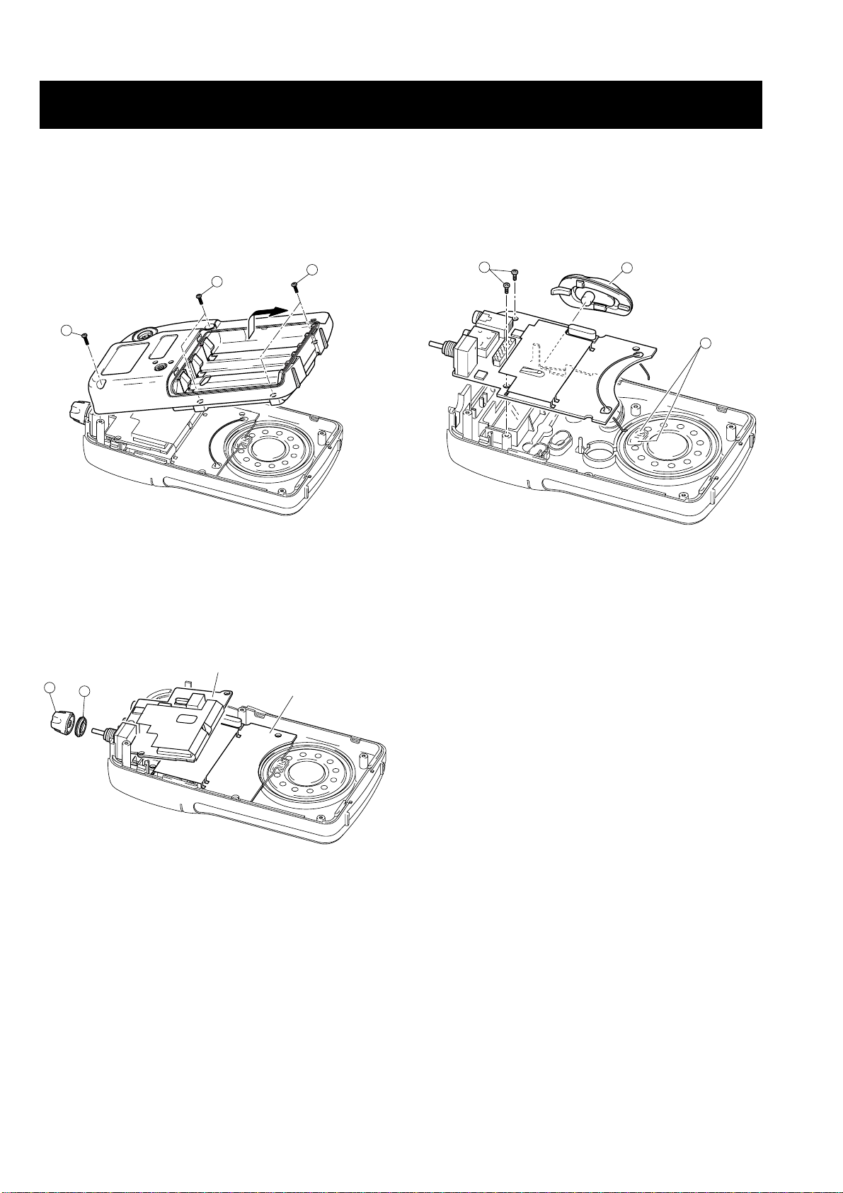
SECTION 3 DISASEMBLY INSTRUCTION
3 - 1
A
B
B
MAIN unit
RF unit
C
D
E
G
F
•
REMOVING THE REAR PANEL
1 Unscrew 1 screw A , and 4 screws B.
2 Remove the rear panel in the direction of the arrow.
•
REMOVING THE RF UNIT
1 Remove 1 knob C, and unscrew 1 nut D.
2 Then remove the RF unit.
•
REMOVING THE MAIN UNIT
1 Unscrew 2 screws, E.
2 Remove the PTT rubber, F.
3 Unsolder 2 points, G, and remove the MAIN unit.
Page 7
4 - 1
SECTION 4 CIRCUIT DESCRIPTION
4-1 RECEIVER CIRCUITS
4-1-1 ANTENNA SWITCHING CIRCUIT (RF UNIT)
Received signals from the antenna connector are passed
through the low-pass filter (L5, L6, C8–C12). The filtered signals are applied to the λ⁄4 type antenna switching circuit
(D101, D102, L4, L206, C209, C210). The passed signals
are then applied to the RF amplifier circuit.
The antenna switching circuit functions as a low-pass filter
while receiving. However, its impedance becomes very high
while D101 and D102 are turned ON (while transmitting).
Thus transmit signals are blocked from entering the receiver circuits. The passed signals are then applied to the RF
amplifier circuit.
4-1-2 RF CIRCUIT (RF UNIT)
The RF circuit amplifies signals within the range of frequency coverage and filters out-of-band signals.
The signals from the antenna switching circuit are amplified
at the RF amplifier (Q3) and passed through the bandpass
filter (FI1) to suppress out-of-band signals. The filtered signals are applied to the 1st mixer circuit.
4-1-3 1ST MIXER AND 1ST IF CIRCUITS (RF UNIT)
The 1st mixer circuit converts the received signals to a fixed
frequency of the 1st IF signal with a PLL output frequency.
By changing the PLL frequency, only desired signals will
pass through a crystal filter at the next stage of the 1st mixer.
The signals from the bandpass filter (FI1) are mixed at the
1st mixer circuit (Q2) with a 1st LO signal coming from the
VCO circuit to produce a 21.7 MHz 1st IF signal.
The 1st IF signal is applied to a crystal filter (FI2) to suppress out-of-band signals. The filtered 1st IF signal is
applied to the IF amplifier (Q1), then applied to the 2nd
mixer circuit.
4-1-4 2ND MIXER AND DEMODULATOR CIRCUITS
(RF UNIT)
The 2nd mixer circuit converts the 1st IF signal into a 2nd IF
signal. Adouble conversion superheterodyne system (which
converts receive signals twice) improves the image rejection
ratio and obtains stable receiver gain.
The 1st IF signal from the IF amplifier (Q1) is applied to the
2nd mixer section in the FM IF IC (IC2, pin 16), and is mixed
with the 2nd LO signal to be converted into a 450 kHz 2nd
IF signal.
The FM IF IC contains a 2nd mixer, quadrature detector,
noise amplifier and a limiter amplifier, etc. The PLL reference oscillator (X1) is used for the 2nd LO signal via the PLL
IC (IC1, pins 16, 17), and is applied to pin 1 of the FM IF IC
(IC2).
The mixed 2nd IF signal is output from pin 3 (IC2) and
passed through the ceramic bandpass filter (FI3) to remove
unwanted heterodyne frequencies. It is then amplified at the
limiter amplifier section (IC2, pin 5) and applied to the quadrature detector section (IC2, pins 10, 11) to demodulate the
2nd IF signal into AF signals.
4-1-5 AF CIRCUIT (RF AND MAIN UNITS)
AF signals from the FM IF IC (RF unit; IC2, pin 9) are
passed through the high-pass filter (RF unit; Q15, Q16) to
remove CTCSS signals then applied to the MAIN unit via J2
(pin 10) as the “VOL” signal.
The “VOL” signal (AF signals) from the RF unit is applied to
the [VOL] control (MAIN unit; R58) to control the audio level
via the volume mute switch (Q23). The level controlled AF
signals are applied to the AF power amplifier (IC9, pin 2) to
drive an internal speaker (SP1) via the [SP] jack (J1).
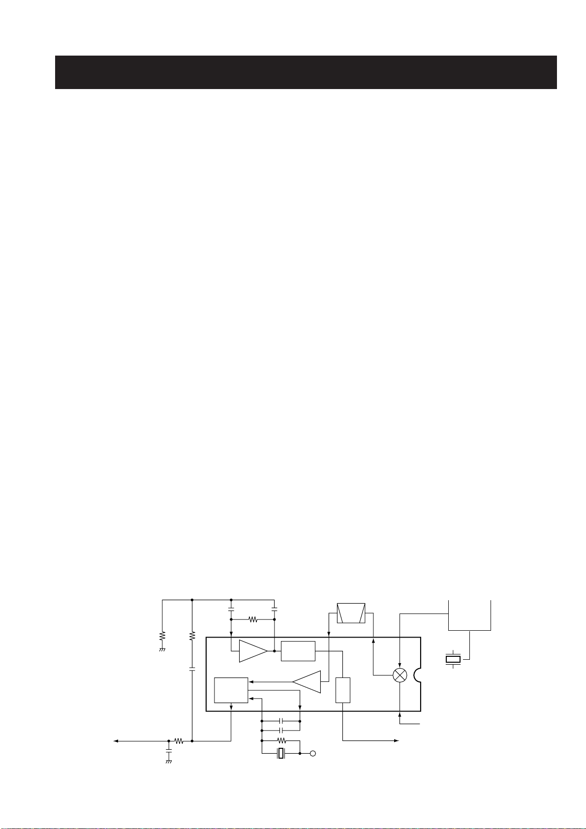
• 2nd IF and demodulator circuits
Mixer
16
Limiter
amp.
2nd IF filter
450 kHz
PLL IC
IC1
X1
21.25 MHz
X2
(21.25 MHz)
RSSI
IC2 TA31136FN
14
1st IF (21.7 MHz)
from Q1
"SQL" signal to the CPU pin 59
11109
87 5 3
AF signal "AF"
R+3
1
17
16
Active
filter
FI3
Noise
detector
FM
detector
Page 8
4 - 2
4-1-6 SQUELCH CIRCUIT (RF AND MAIN UNITS)
• NOISE SQUELCH
The noise squelch circuit cuts out AF signals when no RF
signals are received. By detecting noise components in the
AF signals, the squelch circuit switches the AF mute switch.
A portion of the AF signals from the FM IF IC (RF unit; IC2,
pin 9) are applied to the active filter section (RF unit; IC2,
pin 8). The active filter section amplifies and filters noise
components. The filtered signals are applied to the noise
detector section and output from pin 14 as the “SQL” signal.
The “SQL” signal from IC2 (pin14) is applied to the CPU
(MAIN unit; IC1, pin 59). The CPU analyzes the noise condition and outputs the “RMUT” and “AFON” signals to toggle
the volume mute (MAIN unit; Q23) and AF mute (MAIN unit;
Q5, Q10, Q11) switches.
• TONE SQUELCH
The tone squelch circuit detects AF signals and opens the
squelch only when receiving signal containing a matching
subaudible tone (CTCSS). When tone squelch is in use, and
a signal with a mismatched or no subaudible tone is
received, the tone squelch circuit mutes the AF signals even
when noise squelch is open.
A portion of the AF signals from the FM IF IC (RF unit; IC2,
pin 9) passes through the tone low-pass filter (MAIN unit;
Q7, Q12) to remove AF (voice) signals and is applied to the
CTCSS decoder inside the CPU (MAIN unit; IC1, pin 58) via
the “CTCIN” line to control the volume mute and AF mute
switches.
4-2 TRANSMITTER CIRCUITS
4-2-1 MICROPHONE AMPLIFIER CIRCUIT
(MAIN UNIT)
The microphone amplifier circuit amplifies audio signals with
pre-emphasis characteristics from the microphone to a level
needed for the modulation circuit.
AF signals from the internal/external microphone are applied
to the microphone amplifier circuit (IC2b) via the microphone
mute switch (Q6) and pre-emphasis circuit (R7, C24). The
amplified signals are passed through the splatter filter (IC2a)
and applied to the modulation circuit in the RF unit via J4
(pin 6) as the MOD signal.
4-2-2 MODULATION CIRCUIT (RF UNIT)
The modulation circuit modulates the VCO oscillating signal
(RF signal) using the microphone AF signals.
The filtered audio signals from the MAIN unit are passed
through the deviation adjustment pot (R50), and are then
applied to the modulation circuit (D4, D5) to modulate transmit signals at the VCO circuit (Q6).
The modulated signal is applied to the drive amplifier circuit.
4-2-3 DRIVE/POWER AMPLIFIER CIRCUITS
(RF UNIT)
The amplifier circuit amplifies the VCO oscillating signal to
the output power level.
The signal from the buffer amplifiers (Q7, Q203) is passed
through the Tx/Rx switching circuit (D2), and are amplified at
the pre-drive (Q8) and drive (Q201) amplifiers. The amplified
signal is power-amplified at the power amplifier (Q202) to
obtain 500 mW of RF power
The amplified transmit signal is passed through the antenna
switching circuit (D7) and low-pass filter, and is then applied
to the antenna.
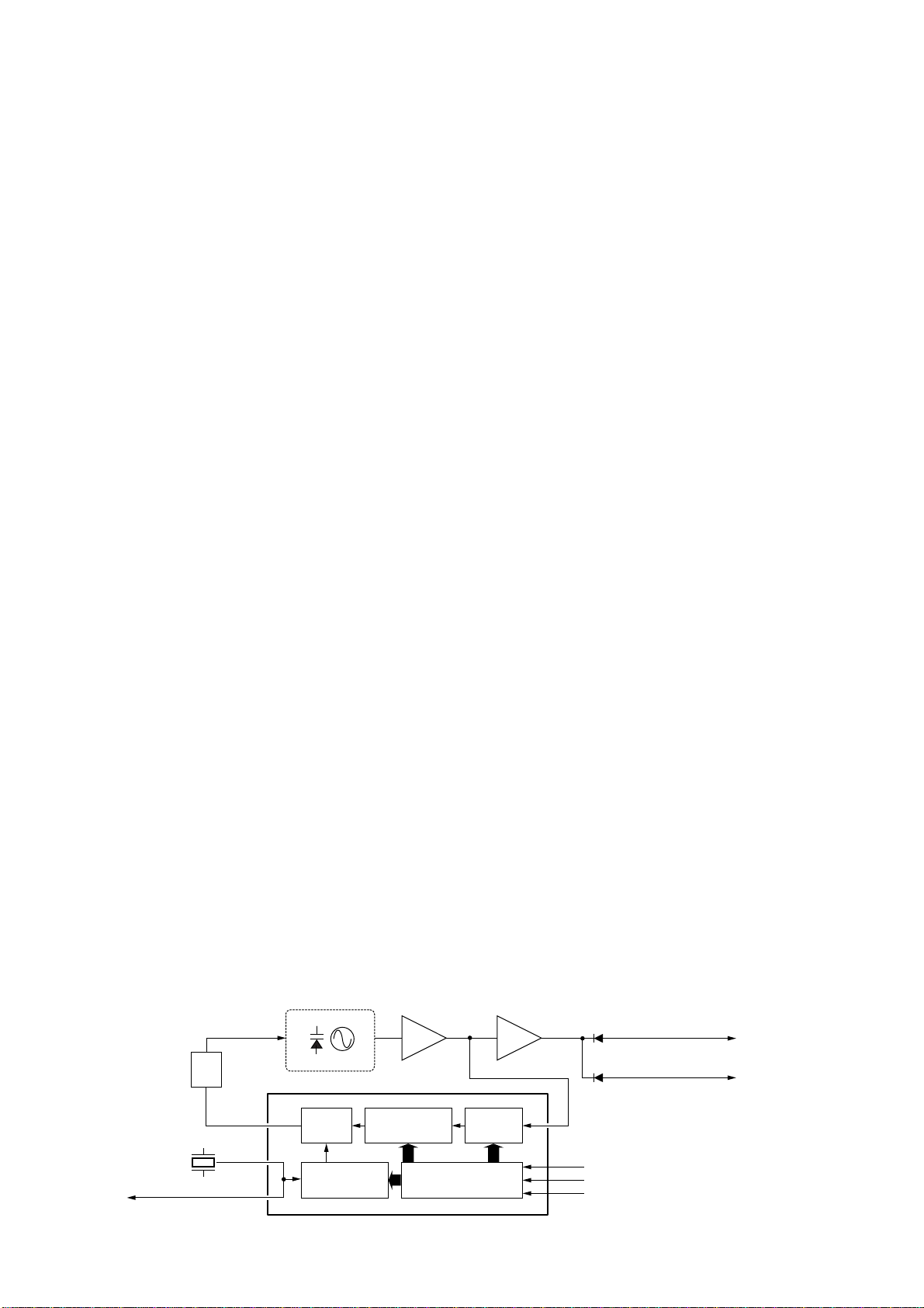
4-3 PLL CIRCUITS (RF UNIT)
A PLL circuit provides stable oscillation of the transmit frequency and receive 1st LO frequency. The PLL output compares the phase of the divided VCO frequency to the reference frequency. The PLL output frequency is controlled by
the divided ratio (N-data) of a programmable divider.
The PLL circuit consists of the VCO circuit (Q6). An oscillated signal from the VCO passes through the buffer amplifier
(Q7), and is then applied to the PLL IC (IC1, pin19) and
prescaled in the PLL IC based on the divided ratio (N-data).
The reference signal is generated at the reference oscillator
(X1) and is applied to the PLL IC. The PLL IC detects the
out-of-step phase using the reference frequency and outputs it from pin 13 (IC1). The output signal is passed through
the loop filter (R45, C68) and is then applied to the VCO circuit as the lock voltage.
If the oscillated signal drifts, its phase changes from that of
the reference frequency, causing a lock voltage change to
compensate for the drift in the oscillated frequency.
• PLL circuit
Shift register
Prescaler
Phase
detector
Loop
filter
Programmable
counter
Programmable
divider
X1
21.25 MHz
to the FM IF IC
VCO
Buffer
Q7
3
4
5
STB
IC1 (PLL IC)
CK
DATA
to transmitter circuit
to 1st mixer circuit
D2
D1
17
16
14
19
Q6, D4, D5
Buffer
Q203
Page 9
4 - 3
4-4 POWER SUPPLY CIRCUITS
VOLTAGE LINE
4-5 PORT ALLOCATIONS
4-5-1 CPU (MAIN unit; IC1)
LINE
BATT
3V
+3V
R+3
T+3
DESCRIPTION
The voltage from the connected battery cells.
Common 3 V converted from the BATT line at
the 3V regulator circuit (IC6). The circuit outputs
the voltage regardless of the power ON/OFF
condition.
Common 3 V converted from the BATT line at
the +3V regulator circuit (Q25, D4).
Receive 3 V cotrolled by the R+3 regulator circuit
(Q18) using the “RXV” signal from CPU (IC1).
Transmit 3 V converted from the BATT line at the
T+3 regulator circuit (Q27, Q28, Q101, D5) using
the “TXV” signal coming from CPU (IC1).
Outputs data signals to the PLL IC (RF
unit; IC1).
Outputs strobe signals for the PLL IC
(RF unit; IC1).
Outputs control signal for the +3V regulator circuit (MAIN unit; Q25, D4).
Output port for the CTCSS signals.
Outputs control signal for the micro-
phone amplifier (IC2).
Low : While microphone amplifier is
ON.
Input port for the CTCSS decode signals.
Input port for squelch level signal.
Input ports for the control signal from
the external remote microphone.
Input port from the connected battery
pack for low battery indication.
Input port for the RSSI signal from the
FM IF IC (RF unit; IC2) to detect receiving signal strength level.
Outputs clock signal to the EEPROM
(IC3).
Outputs data signals to the EEPROM
(IC3).
Output port for power save function,
applied to VCO regurator circuit (RF
unit; Q13, Q14, D8, D9).
Outputs the R+3 regulator control signal (Q25, D4).
Outputs the T+3 regulator control signal (Q27, Q28, Q101, D5).
Outputs control signal for LCD backlight.
Low : While LCD backlight is ON.
Outputs internal microphone control
signal.
High : While internal PTT switch is
pushed.
Outputs MIC mute signal for RING
function.
High : While RING signals are out-
put, etc.
51
52
53
54–56
57
58
59
60
61
62
73
74
75
76
77
78
79
80
PLLDA
PLLST
POWER
CTCO0–
CTCO2
TXMOD
CTCIN
SQLIN
REMIN
BATIN
SENIN
EEPCK
EEPDA
PSC
RXV
TXV
LAMPC
MICSW
MMUTE
Pin Port
Description
number name
Outputs VCO oscillation frequency
control signal for Tx/Rx.
Low : While transmitting
Input port for the PTT switch from the
external mic jack (MAIN unit; J1).
Low : External PTT switch is ON.
Input port for the internal PTT switch.
Low : While PTT switch is pushed.
Input port for the [DOWN] switch.
Input port for the [UP] switch.
Input port for the [MODE] switch.
Input port for the POWER switch.
Low : While POWER switch is
pushed.
Outputs beep audio signal.
Outputs volume mute switch (Q23)
control signal.
High : While squelched
Outputs control signal for the AF amplifier regulator circuit (Q5, Q10, Q11).
High: When squelch is open.
Outputs clock signal to the PLL IC (RF
unit; IC1).
4
31
34
35
36
37
38
46
48
49
50
SHIFT
PTT2
PTT1
DOWN
UP
MODE
POWSW
BEEP
RMUTE
AFON
PLLCK
Pin Port
Description
number name
Page 10

5 - 2
SECTION 5 ADJUSTMENT PROCEDURES
5-1 PREPARATION
■ REQUIRED TEST EQUIPMENT
EQUIPMENT
DC power supply
Frequency counter
FM deviation meter
DC voltmeter
RF power meter
(terminated type)
GRADE AND RANGE
Output voltage : 4.5 V DC
Current capacity : 1 Aor more
Frequency range : 0.1–600 MHz
Frequency accuracy: ±1 ppm or better
Sensitivity : 100 mV or better
Frequency range : 30–600 MHz
Measuring range : 0 to ±10 kHz
Input impedance : 50 kΩ/V DC or better
Measuring range : 100 mW–1 W
Frequency range : 300–600 MHz
Impedance : 50 Ω
SWR : Less than 1.2 : 1
EQUIPMENT
Audio generator
Standard signal
generator (SSG)
Oscilloscope
AC millivoltmeter
External speaker
Attenuator
GRADE AND RANGE
Frequency range : 300–3000 Hz
Measuring range : 1–500 mV
Frequency range : 0.1–600 MHz
Output level : 0.1 µV–32 mV
(–127 to –17 dBm)
Frequency range : DC–20 MHz
Measuring range : 0.01–10 V
Measuring range : 10 mV–10 V
Input impedance : 8 Ω
Capacity : 300 mW or more
Power attenuation : 30 or 40 dB
Capacity : 1 W or more
■ ENTERING THE ADJUSTMENT MODE
q Turn the transceiver power OFF.
w While connecting the “TEST” and GND on the MAIN unit, then turn power ON.
(See location at page 5-3)
■ CONNECTIONS
to the RF test port J1
Standard signal
generator
–17 to –127 dBm
(32 mV to 0.1 µV)
CAUTION:
DO NOT transmit while SSG is
connected to the antenna connector.
Frequency
counter
FM deviation
meter
Attenuator
30 dB or 40 dB
RF power meter
50 Ω/100 mW–1 W
DC power supply
4.5 V/1.0 A
–
+
Page 11

5 - 3
REFERENCE
FREQUENCY
OUTPUT
POWER
FM
DEVIATION
5-2 PLL AND TRANSMITTER ADJUSTMENTS
ADJUSTMENT
ADJUSTMENT ADJUSTMENT CONDITION
MEASUREMENT
VALUE
POINT
UNIT LOCATION UNIT ADJUST
466.00625 MHz
470 mW
±2.45 kHz
10 mV ±3dB
1
1
1
2
• Operating channel : Ch 01
• Transmitting
• Operating channel : Ch 01
• Transmitting
• Operating channel : Ch 01
• Set group No. : 01
• Connect an audio generator to the
[MIC] jack and set as:
1 kHz/100 mV rms
• Set an FM deviation meter as:
HPF : OFF
LPF : 20 kHz or 15 kHz
De-emphasis : OFF
Detector : (P–P)/2
• Transmitting
• Set group No. : OFF (– –)
• Set an audio generator output level
until the deviation is ±1.75 kHz.
• Transmitting
Top
panel
RF
RF
Loosely couple a frequency counter to the
antenna.
Connect an RF power
meter to the RF test
port J1.
Connect an FM deviation meter to the RF
test port J1.
RF
RF
RF
C63
R206
R50
Verify
RF
GND
J1
RF test port
R50
FM deviation adjustment
Reference frequency
adjustment
R206
Output power
adjustment
TEST
C63
Page 12

5 - 4
SQUELCH
5-3 RECEIVER ADJUSTMENT
ADJUSTMENT ADJUSTMENT CONDITION
MEASUREMENT
VALUE ADJUSTMENT
UNIT LOCATION
Audio signal
disappears.
12• Operating channel : Ch 04
• Connect an SSG to J1 on the RF unit
and set as:
Frequency : 446.04375 MHz
Level : 0.14 µV*
(–124 dBm)
Modulation : OFF
• Receiving
• Set an SSG as :
Level : OFF
• Receiving
Front
panel
Internal speaker
Push and hold
[MODE] and
[DOWN] keys for
1 sec.
Verify
Page 13

[MAIN UNIT][MAIN UNIT]
IC1 1140008770 S.IC µPD753036GK-559-BE9
IC2 1110002820 S.IC NJM2100M-T1
IC3 1140008350 S.IC AT24C02N-10SI-2.7
IC5 1110004710 S.IC S-80928ANMP-DDR-T2
IC6 1180001150 S.IC S-81230SG-QB-T1
IC9 1110002810 S.IC NJM2070M-T1
Q1 1590000720 S.TRANSISTOR DTA144EUA T106
Q2 1590001440 S.TRANSISTOR UN9214 (TX)
Q3 1590002920 S.TRANSISTOR DTA123JUA T106
Q5 1510000580 S.TRANSISTOR 2SA1362-GR (TE85R)
Q6 1560000840 S.FET 2SK1829 (TE85R)
Q7 1530002280 S.TRANSISTOR 2SC4081 T107 S
Q10 1530002280 S.TRANSISTOR 2SC4081 T107 S
Q11 1530003090 S.TRANSISTOR 2SC4213-B (TE85R)
Q12 1530002280 S.TRANSISTOR 2SC4081 T107 S
Q14 1590001330 S.TRANSISTOR DTA114EUAT106
Q18 1510000770 S.TRANSISTOR 2SA1586-GR (TE85R)
Q23 1590001390 S.FET 2SJ144-Y (TE85R)
Q25 1590002490 S.TRANSISTOR UMZ2N TR
Q27 1530002280 S.TRANSISTOR 2SC4081 T107 S
Q28 1520000200 S.TRANSISTOR 2SB798-T2 DK
Q29 1590000680 S.TRANSISTOR DTC114EUA T106
Q101 1590002630 S.TRANSISTOR UMZ1N TR
D2 1750000550 S.DIODE 1SS355 TE-17
D4 1750000550 S.DIODE 1SS355 TE-17
D5 1750000550 S.DIODE 1SS355 TE-17
X1 6050010450 S.XTAL CR-627 (5.8368 MHz)
R2 7030003670 S.RESISTOR ERJ3GEYJ 823 V (82 kΩ)
R4 7030003670 S.RESISTOR ERJ3GEYJ 823 V (82 kΩ)
R5 7030003810 S.RESISTOR ERJ3GEYJ 125 V (1.2 MΩ)
R6 7030003710 S.RESISTOR ERJ3GEYJ 184 V (180 kΩ)
R7 7030003450 S.RESISTOR ERJ3GEYJ 122 V (1.2 kΩ)
R9 7030003680 S.RESISTOR ERJ3GEYJ 104 V (100 kΩ)
R10 7030003310 S.RESISTOR ERJ3GEYJ 820 V (82 Ω)
R12 7030003200 S.RESISTOR ERJ3GEYJ 100 V (10 Ω)
R13 7030003520 S.RESISTOR ERJ3GEYJ 472 V (4.7 kΩ)
R14 7030003500 S.RESISTOR ERJ3GEYJ 332 V (3.3 kΩ)
R22 7030003620 S.RESISTOR ERJ3GEYJ 333 V (33 kΩ)
R23 7030003580 S.RESISTOR ERJ3GEYJ 153 V (15 kΩ)
R24 7030003820 S.RESISTOR ERJ3GEYJ 155 V (1.5 MΩ)
R25 7030003570 S.RESISTOR ERJ3GEYJ 123 V (12 kΩ)
R26 7030003560 S.RESISTOR ERJ3GEYJ 103 V (10 kΩ)
R27 7030003320 S.RESISTOR ERJ3GEYJ 101 V (100 Ω)
R30 7030003580 S.RESISTOR ERJ3GEYJ 153 V (15 kΩ)
R31 7030003800 S.RESISTOR ERJ3GEYJ 105 V (1 MΩ)
R32 7030003780 S.RESISTOR ERJ3GEYJ 684 V (680 kΩ)
R33 7030003540 S.RESISTOR ERJ3GEYJ 682 V (6.8 kΩ)
R34 7030003540 S.RESISTOR ERJ3GEYJ 682 V (6.8 kΩ)
R35 7030003530 S.RESISTOR ERJ3GEYJ 562 V (5.6 kΩ)
R36 7030003560 S.RESISTOR ERJ3GEYJ 103 V (10 kΩ)
R37 7030003600 S.RESISTOR ERJ3GEYJ 223 V (22 kΩ)
R38 7030003600 S.RESISTOR ERJ3GEYJ 223 V (22 kΩ)
R39 7030003670 S.RESISTOR ERJ3GEYJ 823 V (82 kΩ)
R40 7030003680 S.RESISTOR ERJ3GEYJ 104 V (100 kΩ)
R41 7030003530 S.RESISTOR ERJ3GEYJ 562 V (5.6 kΩ)
R42 7030003500 S.RESISTOR ERJ3GEYJ 332 V (3.3 kΩ)
R43 7030003650 S.RESISTOR ERJ3GEYJ 563 V (56 kΩ)
R45 7030003840 S.RESISTOR ERJ3GEYJ 225 V (2.2 MΩ)
R46 7030003320 S.RESISTOR ERJ3GEYJ 101 V (100 Ω)
R49 7030003320 S.RESISTOR ERJ3GEYJ 101 V (100 Ω)
R50 7030003520 S.RESISTOR ERJ3GEYJ 472 V (4.7 kΩ)
R51 7030003760 S.RESISTOR ERJ3GEYJ 474 V (470 kΩ)
R52 7030003740 S.RESISTOR ERJ3GEYJ 334 V (330 kΩ)
R53 7030003820 S.RESISTOR ERJ3GEYJ 155 V (1.5 MΩ)
R54 7030003450 S.RESISTOR ERJ3GEYJ 122 V (1.2 kΩ)
R55 7030003330 S.RESISTOR ERJ3GEYJ 121 V (120 Ω)
R56 7030004050 S.RESISTOR ERJ3GEYJ 1R0 V (1 Ω)
R57 7030003580 S.RESISTOR ERJ3GEYJ 153 V (15 kΩ)
S.=Surface mount
R58 7210001970 VARIABLE RV-244
R59 7030003680 S.RESISTOR ERJ3GEYJ 104 V (100 kΩ)
R61 7030003280 S.RESISTOR ERJ3GEYJ 470 V (47 Ω)
R62 7030003680 S.RESISTOR ERJ3GEYJ 104 V (100 kΩ)
R63 7030003530 S.RESISTOR ERJ3GEYJ 562 V (5.6 kΩ)
R64 7030003590 S.RESISTOR ERJ3GEYJ 183 V (18 kΩ)
R65 7030003590 S.RESISTOR ERJ3GEYJ 183 V (18 kΩ)
R66 7030003590 S.RESISTOR ERJ3GEYJ 183 V (18 kΩ)
R67 7030003590 S.RESISTOR ERJ3GEYJ 183 V (18 kΩ)
R68 7030003590 S.RESISTOR ERJ3GEYJ 183 V (18 kΩ)
R69 7030003590 S.RESISTOR ERJ3GEYJ 183 V (18 kΩ)
R70 7030003660 S.RESISTOR ERJ3GEYJ 683 V (68 kΩ)
R71 7030003620 S.RESISTOR ERJ3GEYJ 333 V (33 kΩ)
R72 7030003800 S.RESISTOR ERJ3GEYJ 105 V (1 MΩ)
R74 7030003560 S.RESISTOR ERJ3GEYJ 103 V (10 kΩ)
R76 7030003680 S.RESISTOR ERJ3GEYJ 104 V (100 kΩ)
R77 7030003400 S.RESISTOR ERJ3GEYJ 471 V (470 Ω)
R78 7030003560 S.RESISTOR ERJ3GEYJ 103 V (10 kΩ)
R79 7030003720 S.RESISTOR ERJ3GEYJ 224 V (220 kΩ)
R80 7030003680 S.RESISTOR ERJ3GEYJ 104 V (100 kΩ)
R81 7030003560 S.RESISTOR ERJ3GEYJ 103 V (10 kΩ)
R86 7030003680 S.RESISTOR ERJ3GEYJ 104 V (100 kΩ)
R87 7030003800 S.RESISTOR ERJ3GEYJ 105 V (1 MΩ)
R88 7030003680 S.RESISTOR ERJ3GEYJ 104 V (100 kΩ)
R89 7030003440 S.RESISTOR ERJ3GEYJ 102 V (1 kΩ)
R90 7030003440 S.RESISTOR ERJ3GEYJ 102 V (1 kΩ)
R94 7030003720 S.RESISTOR ERJ3GEYJ 224 V (220 kΩ)
R95 7030003520 S.RESISTOR ERJ3GEYJ 472 V (4.7 kΩ)
R96 7030003680 S.RESISTOR ERJ3GEYJ 104 V (100 kΩ)
R97 7030003680 S.RESISTOR ERJ3GEYJ 104 V (100 kΩ)
R98 7030003680 S.RESISTOR ERJ3GEYJ 104 V (100 kΩ)
R99 7030003680 S.RESISTOR ERJ3GEYJ 104 V (100 kΩ)
R100 7030003680 S.RESISTOR ERJ3GEYJ 104 V (100 kΩ)
R101 7030003680 S.RESISTOR ERJ3GEYJ 104 V (100 kΩ)
R102 7030003680 S.RESISTOR ERJ3GEYJ 104 V (100 kΩ)
R103 7030003680 S.RESISTOR ERJ3GEYJ 104 V (100 kΩ)
R105 7030003560 S.RESISTOR ERJ3GEYJ 103 V (10 kΩ)
R106 7030003560 S.RESISTOR ERJ3GEYJ 103 V (10 kΩ)
R108 7030003620 S.RESISTOR ERJ3GEYJ 333 V (33 kΩ)
R110 7030003800 S.RESISTOR ERJ3GEYJ 105 V (1 MΩ)
R112 7030003560 S.RESISTOR ERJ3GEYJ 103 V (10 kΩ)
R114 7030003500 S.RESISTOR ERJ3GEYJ 332 V (3.3 kΩ)
R115 7030003410 S.RESISTOR ERJ3GEYJ 561 V (560 Ω)
R117 7030003680 S.RESISTOR ERJ3GEYJ 104 V (100 kΩ)
R118 7030003520 S.RESISTOR ERJ3GEYJ 472 V (4.7 kΩ)
R119 7030003680 S.RESISTOR ERJ3GEYJ 104 V (100 kΩ)
R200 7030003840 S.RESISTOR ERJ3GEYJ 225 V (2.2 MΩ)
R201 7030003370 S.RESISTOR ERJ3GEYJ 271 V (270 Ω)
R202 7030003320 S.RESISTOR ERJ3GEYJ 101 V (100 Ω)
R203 7030003550 S.RESISTOR ERJ3GEYJ 822 V (8.2 kΩ)
R204 7030003540 S.RESISTOR ERJ3GEYJ 682 V (6.8 kΩ)
C1 4030008470 S.CERAMIC C1608 JB 1H 272K-T-A
C3 4030011600 S.CERAMIC C1608 JB 1C 104KT-N
C4 4030011600 S.CERAMIC C1608 JB 1C 104KT-N
C5 4030006850 S.CERAMIC C1608 JB 1H 471K-T-A
C6 4030008680 S.CERAMIC C2012 JF 1C 105Z-T-A
C7 4030011600 S.CERAMIC C1608 JB 1C 104KT-N
C8 4510004630 S.ELECTROLYTIC ECEV1CA100SR
C9 4030006850 S.CERAMIC C1608 JB 1H 471K-T-A
C10 4030006850 S.CERAMIC C1608 JB 1H 471K-T-A
C11 4030006850 S.CERAMIC C1608 JB 1H 471K-T-A
C15 4030011600 S.CERAMIC C1608 JB 1C 104KT-N
C17 4550006880 S.TANTALUM TEMSVD2 0J 157M-12R
C18 4510004630 S.ELECTROLYTIC ECEV1CA100SR
C20 4030011600 S.CERAMIC C1608 JB 1C 104KT-N
C21 4030011600 S.CERAMIC C1608 JB 1C 104KT-N
C24 4030008900 S.CERAMIC C1608 JB 1C 333K-T-A
C25 4030006850 S.CERAMIC C1608 JB 1H 471K-T-A
C26 4030006850 S.CERAMIC C1608 JB 1H 471K-T-A
C27 4030011600 S.CERAMIC C1608 JB 1C 104KT-N
C28 4030008920 S.CERAMIC C1608 JB 1C 473K-T-A
C29 4030007150 S.CERAMIC C1608 CH 1H 151J-T-A
C31 4030008880 S.CERAMIC C1608 JB 1C 223K-T-A
C32 4030011600 S.CERAMIC C1608 JB 1C 104KT-N
6 - 1
SECTION 6 PARTS LIST
REF ORDER
DESCRIPTION
NO. NO.
REF ORDER
DESCRIPTION
NO. NO.
Page 14

IC1 1130007610 S.IC µPD3140GS-E1 (DS8)
IC2 1110003200 S.IC TA31136FN (EL)
Q1 1530002600 S.TRANSISTOR 2SC4215-O (TE85R)
Q2 1580000670 S.FET 3SK284 (TE85R)
Q3 1530002920 S.TRANSISTOR 2SC4226-T2 R25
Q6 1530003320 S.TRANSISTOR 2SC5108-Y (TE85R)
Q7 1530003320 S.TRANSISTOR 2SC5108-Y (TE85R)
Q8 1530002940 S.TRANSISTOR 2SC4228-T2 R44
Q12 1530003260 S.TRANSISTOR 2SC5006-T1
Q13 1530002280 S.TRANSISTOR 2SC4081 T107 S
Q14 1510000770 S.TRANSISTOR 2SA1586-GR (TE85R)
Q15 1530002280 S.TRANSISTOR 2SC4081 T107 S
Q16 1530002280 S.TRANSISTOR 2SC4081 T107 S
Q201 1530000372 S.TRANSISTOR 2SC3356 R24-T2B
Q202 1590002890 S.FET XRF9482T1
Q203 1530003320 S.TRANSISTOR 2SC5108-Y (TE85R)
D1 1790000620 S.DIODE MA77 (TX)
D2 1790000620 S.DIODE MA77 (TX)
D4 1720000640 S.VARICAP 1SV284 (TPH3)
D5 1720000640 S.VARICAP 1SV284 (TPH3)
D7 1790001260 S.DIODE MA2S077-(TX)
D8 1750000550 S.DIODE 1SS355 TE-17
D9 1750000550 S.DIODE 1SS355 TE-17
D101 1790001260 S.DIODE MA2S077-(TX)
D102 1790001260 S.DIODE MA2S077-(TX)
D103 1790001240 S.DIODE MA2S728-(TX)
FI1 2040001580 S.SAW NSVS647
FI2 2010002320 MONOLITH FL-297 (21.700 MHz)
FI3 2020001410 CERAMIC CFWM450G
X1 6050010900 S.XTAL CR-669 (21.2500 MHz)
X2 6070000210 S.DISCRIMINATOR CDBCA450CX24
L1 6200003280 S.COIL NL 252018T-2R2J
L3 6200007570 S.COIL LL1608-FH18NJ
L4 6200005670 S.COIL ELJRE 12NG-F
L5 6200008270 S.COIL 0.26-1.0-5TL 17N
L6 6200008270 S.COIL 0.26-1.0-5TL 17N
L10 6200005700 S.COIL ELJRE 22NG-F
L11 6200003640 S.COIL MLF1608K 100K-T
L12 6200003640 S.COIL MLF1608K 100K-T
L13 6200002350 S.COIL LQN 1A 27NJ04
L14 6200005720 S.COIL ELJRE 33NG-F
L15 6200007000 S.COIL ELJRE 82NG-F
L21 6200007580 S.COIL LL1608-FH22NJ
L23 6200008430 S.COIL 0.20-1.0-4TL 15N
L25 6200002190 S.COIL MLF2012A 4R7K-T
L201 6200007580 S.COIL LL1608-FH22NJ
L202 6200005720 S.COIL ELJRE 33NG-F
L203 6200007730 S.COIL LQN21A 39NJ04
L204 6200008440 S.COIL LQN21A 8N2D04
L205 6200006670 S.COIL ELJRE 68NG-F
L206 6200005690 S.COIL ELJRE 18NG-F
L208 6200003640 S.COIL MLF1608K 100K-T
L209 6200006980 S.COIL ELJRE R10G-F
L210 6200007600 S.COIL LL1608-FH33NJ
L211 6200007590 S.COIL LL1608-FH27NJ
R1 7030003430 S.RESISTOR ERJ3GEYJ 821 V (820 Ω)
R2 7030003670 S.RESISTOR ERJ3GEYJ 823 V (82 kΩ)
R3 7030003440 S.RESISTOR ERJ3GEYJ 102 V (1 kΩ)
R4 7030003410 S.RESISTOR ERJ3GEYJ 561 V (560 Ω)
R6 7030003520 S.RESISTOR ERJ3GEYJ 472 V (4.7 kΩ)
R7 7030003280 S.RESISTOR ERJ3GEYJ 470 V (47 Ω)
R10 7030003550 S.RESISTOR ERJ3GEYJ 822 V (8.2 kΩ)
R12 7030003440 S.RESISTOR ERJ3GEYJ 102 V (1 kΩ)
R16 7030003260 S.RESISTOR ERJ3GEYJ 330 V (33 Ω)
R19 7030003380 S.RESISTOR ERJ3GEYJ 331 V (330 Ω)
R25 7030003620 S.RESISTOR ERJ3GEYJ 333 V (33 kΩ)
R27 7030003680 S.RESISTOR ERJ3GEYJ 104 V (100 kΩ)
R29 7030003280 S.RESISTOR ERJ3GEYJ 470 V (47 Ω)
R30 7030003620 S.RESISTOR ERJ3GEYJ 333 V (33 kΩ)
R31 7030003620 S.RESISTOR ERJ3GEYJ 333 V (33 kΩ)
[RF UNIT][MAIN UNIT]
S.=Surface mount
C34 4030006880 S.CERAMIC C1608 JB 1H 472K-T-A
C35 4030011600 S.CERAMIC C1608 JB 1C 104KT-N
C36 4030006860 S.CERAMIC C1608 JB 1H 102K-T-A
C40 4030011600 S.CERAMIC C1608 JB 1C 104KT-N
C42 4030006900 S.CERAMIC C1608 JB 1E 103K-T-A
C44 4030011600 S.CERAMIC C1608 JB 1C 104KT-N
C45 4030009650 S.CERAMIC C1608 CH 1H 240J-T-A
C46 4030009650 S.CERAMIC C1608 CH 1H 240J-T-A
C47 4030006850 S.CERAMIC C1608 JB 1H 471K-T-A
C48 4510005430 S.ELECTROLYTIC ECEV0JA220SR
C49 4030011600 S.CERAMIC C1608 JB 1C 104KT-N
C50 4030011600 S.CERAMIC C1608 JB 1C 104KT-N
C51 4030011600 S.CERAMIC C1608 JB 1C 104KT-N
C52 4510005860 S.ELECTROLYTIC ECEV1HA2R2SR
C53 4030011600 S.CERAMIC C1608 JB 1C 104KT-N
C54 4030011600 S.CERAMIC C1608 JB 1C 104KT-N
C55 4510005870 S.ELECTROLYTIC ECEV1HA3R3SR
C56 4030011600 S.CERAMIC C1608 JB 1C 104KT-N
C57 4030011600 S.CERAMIC C1608 JB 1C 104KT-N
C59 4030006850 S.CERAMIC C1608 JB 1H 471K-T-A
C60 4030011600 S.CERAMIC C1608 JB 1C 104KT-N
C61 4030011600 S.CERAMIC C1608 JB 1C 104KT-N
C62 4030011600 S.CERAMIC C1608 JB 1C 104KT-N
C63 4030011600 S.CERAMIC C1608 JB 1C 104KT-N
C64 4510005430 S.ELECTROLYTIC ECEV0JA220SR
C65 4030011600 S.CERAMIC C1608 JB 1C 104KT-N
C67 4030009590 S.CERAMIC C2012 JF 1C 225Z-T-A
C71 4030011600 S.CERAMIC C1608 JB 1C 104KT-N
C72 4030006900 S.CERAMIC C1608 JB 1E 103K-T-A
C73 4030008650 S.CERAMIC C1608 JB 1H 332K-T-A
C74 4030006860 S.CERAMIC C1608 JB 1H 102K-T-A
C75 4030006860 S.CERAMIC C1608 JB 1H 102K-T-A
C79 4030011600 S.CERAMIC C1608 JB 1C 104KT-N
C80 4510005900 S.ELECTROLYTIC ECEV0GA101SR
C81 4030008900 S.CERAMIC C1608 JB 1C 333K-T-A
C82 4030008920 S.CERAMIC C1608 JB 1C 473K-T-A
C83 4030011600 S.CERAMIC C1608 JB 1C 104KT-N
C85 4030011600 S.CERAMIC C1608 JB 1C 104KT-N
C86 4030008960 S.CERAMIC C2012 JB 1C 104K-T-A
C87 4030006850 S.CERAMIC C1608 JB 1H 471K-T-A
C88 4030006850 S.CERAMIC C1608 JB 1H 471K-T-A
C89 4030006850 S.CERAMIC C1608 JB 1H 471K-T-A
C90 4030006850 S.CERAMIC C1608 JB 1H 471K-T-A
C91 4030006850 S.CERAMIC C1608 JB 1H 471K-T-A
C92 4030006850 S.CERAMIC C1608 JB 1H 471K-T-A
C93 4030010760 S.CERAMIC C1608 CH 1H 331J-T-A
C94 4030010760 S.CERAMIC C1608 CH 1H 331J-T-A
C95 4030010760 S.CERAMIC C1608 CH 1H 331J-T-A
C96 4030010760 S.CERAMIC C1608 CH 1H 331J-T-A
C97 4030010760 S.CERAMIC C1608 CH 1H 331J-T-A
C98 4030010760 S.CERAMIC C1608 CH 1H 331J-T-A
C99 4030008650 S.CERAMIC C1608 JB 1H 332K-T-A
J1 6450000130 CONNECTOR HSJ1102-01-540
J3 6450001060 CONNECTOR HSJ1493-01-010
J4 6510017950 S.CONNECTOR 4-175638-4
DS1 5010000120 S.LED LN1371G-(TR)
DS2 5030001750 LCD LD-BU10503J
MC1 7700002160 MICROPHON KUC3523-040245
S1 2260001900 SWITCH SW-149
W2 7030003860 S.JUMPER ERJ3GE JPW V
W3 7030003860 S.JUMPER ERJ3GE JPW V
W7 7030003860 S.JUMPER ERJ3GE JPW V
EP1 8930045510 LCD CONTACT SRCN-2045-SP-N-W
EP2 0910051962 PCB B 5420B
6 - 2
REF ORDER
DESCRIPTION
NO. NO.
REF ORDER
DESCRIPTION
NO. NO.
Page 15

[RF UNIT][RF UNIT]
S.=Surface mount
R33 7030003550 S.RESISTOR ERJ3GEYJ 822 V (8.2 kΩ)
R34 7030003420 S.RESISTOR ERJ3GEYJ 681 V (680 Ω)
R35 7030003640 S.RESISTOR ERJ3GEYJ 473 V (47 kΩ)
R36 7030003360 S.RESISTOR ERJ3GEYJ 221 V (220 Ω)
R37 7030003600 S.RESISTOR ERJ3GEYJ 223 V (22 kΩ)
R45 7030003550 S.RESISTOR ERJ3GEYJ 822 V (8.2 kΩ)
R50 7310003630 S.TRIMMER EVM-1XSX50 BQ4 (473)
R51 7030003770 S.RESISTOR ERJ3GEYJ 564 V (560 kΩ)
R52 7030003460 S.RESISTOR ERJ3GEYJ 152 V (1.5 kΩ)
R53 7030003700 S.RESISTOR ERJ3GEYJ 154 V (150 kΩ)
R54 7030003560 S.RESISTOR ERJ3GEYJ 103 V (10 kΩ)
R55 7030003580 S.RESISTOR ERJ3GEYJ 153 V (15 kΩ)
R56 7030003580 S.RESISTOR ERJ3GEYJ 153 V (15 kΩ)
R57 7030003480 S.RESISTOR ERJ3GEYJ 222 V (2.2 kΩ)
R58 7030003520 S.RESISTOR ERJ3GEYJ 472 V (4.7 kΩ)
R59 7030003580 S.RESISTOR ERJ3GEYJ 153 V (15 kΩ)
R60 7030003680 S.RESISTOR ERJ3GEYJ 104 V (100 kΩ)
R61 7030003560 S.RESISTOR ERJ3GEYJ 103 V (10 kΩ)
R62 7030003230 S.RESISTOR ERJ3GEYJ 180 V (18 Ω)
R64 7030003650 S.RESISTOR ERJ3GEYJ 563 V (56 kΩ)
R65 7030003500 S.RESISTOR ERJ3GEYJ 332 V (3.3 kΩ)
R66 7030003570 S.RESISTOR ERJ3GEYJ 123 V (12 kΩ)
R67 7030003780 S.RESISTOR ERJ3GEYJ 684 V (680 kΩ)
R68 7030003750 S.RESISTOR ERJ3GEYJ 394 V (390 kΩ)
R69 7030003510 S.RESISTOR ERJ3GEYJ 392 V (3.9 kΩ)
R70 7030003610 S.RESISTOR ERJ3GEYJ 273 V (27 kΩ)
R71 7030003560 S.RESISTOR ERJ3GEYJ 103 V (10 kΩ)
R72 7030003550 S.RESISTOR ERJ3GEYJ 822 V (8.2 kΩ)
R73 7030003780 S.RESISTOR ERJ3GEYJ 684 V (680 kΩ)
R74 7030003750 S.RESISTOR ERJ3GEYJ 394 V (390 kΩ)
R75 7030003560 S.RESISTOR ERJ3GEYJ 103 V (10 kΩ)
R76 7030003510 S.RESISTOR ERJ3GEYJ 392 V (3.9 kΩ)
R83 7030003560 S.RESISTOR ERJ3GEYJ 103 V (10 kΩ)
R86 7030003300 S.RESISTOR ERJ3GEYJ 680 V (68 Ω)
R88 7030003520 S.RESISTOR ERJ3GEYJ 472 V (4.7 kΩ)
R93 7030003200 S.RESISTOR ERJ3GEYJ 100 V (10 Ω)
R202 7030003600 S.RESISTOR ERJ3GEYJ 223 V (22 kΩ)
R205 7030003560 S.RESISTOR ERJ3GEYJ 103 V (10 kΩ)
R206 7310003610 S.TRIMMER EVM-1XSX50 B14 (103)
R207 7030003440 S.RESISTOR ERJ3GEYJ 102 V (1 kΩ)
R208 7030003440 S.RESISTOR ERJ3GEYJ 102 V (1 kΩ)
R209 7030003360 S.RESISTOR ERJ3GEYJ 221 V (220 Ω)
R213 7030003360 S.RESISTOR ERJ3GEYJ 221 V (220 Ω)
R301 7030003550 S.RESISTOR ERJ3GEYJ 822 V (8.2 kΩ)
R302 7030003560 S.RESISTOR ERJ3GEYJ 103 V (10 kΩ)
R303 7030003640 S.RESISTOR ERJ3GEYJ 473 V (47 kΩ)
R304 7030003370 S.RESISTOR ERJ3GEYJ 271 V (270 Ω)
R305 7030003510 S.RESISTOR ERJ3GEYJ 392 V (3.9 kΩ)
R306 7030003550 S.RESISTOR ERJ3GEYJ 822 V (8.2 kΩ)
R310 7030003740 S.RESISTOR ERJ3GEYJ 334 V (330 kΩ)
R311 7030003400 S.RESISTOR ERJ3GEYJ 471 V (470 Ω)
R312 7030003670 S.RESISTOR ERJ3GEYJ 823 V (82 kΩ)
R313 7030003200 S.RESISTOR ERJ3GEYJ 100 V (10 Ω)
C1 4030006860 S.CERAMIC C1608 JB 1H 102K-T-A
C2 4030008920 S.CERAMIC C1608 JB 1C 473K-T-A
C3 4030008920 S.CERAMIC C1608 JB 1C 473K-T-A
C5 4030006850 S.CERAMIC C1608 JB 1H 471K-T-A
C6 4030006850 S.CERAMIC C1608 JB 1H 471K-T-A
C7 4030007050 S.CERAMIC C1608 CH 1H 220J-T-A
C8 4030006970 S.CERAMIC C1608 CH 1H 060D-T-A
C9 4030010780 S.CERAMIC C1608 CH 1H 1R5C-T-A
C10 4030007010 S.CERAMIC C1608 CH 1H 100D-T-A
C11 4030009470 S.CERAMIC C1608 CH 1H R75C-T-A
C12 4030006990 S.CERAMIC C1608 CH 1H 080D-T-A
C13 4030007090 S.CERAMIC C1608 CH 1H 470J-T-A
C16 4030006850 S.CERAMIC C1608 JB 1H 471K-T-A
C17 4340000180 S.MYLAR ECHU 1C 333JB5
C20 4030006850 S.CERAMIC C1608 JB 1H 471K-T-A
C21 4030006850 S.CERAMIC C1608 JB 1H 471K-T-A
C23 4030006980 S.CERAMIC C1608 CH 1H 070D-T-A
C26 4030006850 S.CERAMIC C1608 JB 1H 471K-T-A
C28 4030006850 S.CERAMIC C1608 JB 1H 471K-T-A
C30 4030006980 S.CERAMIC C1608 CH 1H 070D-T-A
C31 4030006980 S.CERAMIC C1608 CH 1H 070D-T-A
C32 4030006970 S.CERAMIC C1608 CH 1H 060D-T-A
C35 4030006860 S.CERAMIC C1608 JB 1H 102K-T-A
C36 4030006990 S.CERAMIC C1608 CH 1H 080D-T-A
C42 4030007010 S.CERAMIC C1608 CH 1H 100D-T-A
C43 4030007040 S.CERAMIC C1608 CH 1H 180J-T-A
C44 4030007060 S.CERAMIC C1608 CH 1H 270J-T-A
C46 4030007020 S.CERAMIC C1608 CH 1H 120J-T-A
C47 4030007050 S.CERAMIC C1608 CH 1H 220J-T-A
C48 4030007050 S.CERAMIC C1608 CH 1H 220J-T-A
C50 4030007020 S.CERAMIC C1608 CH 1H 120J-T-A
C51 4030007020 S.CERAMIC C1608 CH 1H 120J-T-A
C52 4030006930 S.CERAMIC C1608 CH 1H 020C-T-A
C53 4030009540 S.CERAMIC C1608 CH 1H 1R5B-T-A
C54 4030009350 S.CERAMIC C1608 CH 1H 3R5B-T-A
C55 4030006850 S.CERAMIC C1608 JB 1H 471K-T-A
C56 4030006910 S.CERAMIC C1608 CH 1H 0R5C-T-A
C57 4030009520 S.CERAMIC C1608 CH 1H 020B-T-A
C60 4550006350 S.TANTALUM TEMSVB2 1A 226M-8L
C61 4030006960 S.CERAMIC C1608 CH 1H 050C-T-A
C62 4340000180 S.MYLAR ECHU 1C 333JB5
C63 4610002150 S.TRIMMER CTZ3S-10A-W1-AF
C64 4030009660 S.CERAMIC C1608 JF 1C 224Z-T-A
C65 4030006850 S.CERAMIC C1608 JB 1H 471K-T-A
C67 4030011600 S.CERAMIC C1608 JB 1C 104KT-N
C68 4550006590 S.TANTALUM ECST1CY684R
C69 4030006860 S.CERAMIC C1608 JB 1H 102K-T-A
C70 4030006850 S.CERAMIC C1608 JB 1H 471K-T-A
C72 4030006850 S.CERAMIC C1608 JB 1H 471K-T-A
C73 4030011600 S.CERAMIC C1608 JB 1C 104KT-N
C74 4030006850 S.CERAMIC C1608 JB 1H 471K-T-A
C75 4030006850 S.CERAMIC C1608 JB 1H 471K-T-A
C76 4030006850 S.CERAMIC C1608 JB 1H 471K-T-A
C77 4030007050 S.CERAMIC C1608 CH 1H 220J-T-A
C78 4030007110 S.CERAMIC C1608 CH 1H 680J-T-A
C79 4510004630 S.ELECTROLYTIC ECEV1CA100SR
C80 4030009660 S.CERAMIC C1608 JF 1C 224Z-T-A
C81 4030008920 S.CERAMIC C1608 JB 1C 473K-T-A
C82 4030011600 S.CERAMIC C1608 JB 1C 104KT-N
C83 4030008680 S.CERAMIC C2012 JF 1C 105Z-T-A
C84 4030006850 S.CERAMIC C1608 JB 1H 471K-T-A
C85 4550006480 S.TANTALUM TEMSVA 1C 475M-8L
C86 4030011810 S.CERAMIC C1608 JB 1A 224K-T-N
C87 4030011600 S.CERAMIC C1608 JB 1C 104KT-N
C88 4550006250 S.TANTALUM TEMSVA 1A 106M-8L
C89 4030009880 S.CERAMIC C1608 JB 1H 682K-T-A
C90 4030006900 S.CERAMIC C1608 JB 1E 103K-T-A
C91 4030008920 S.CERAMIC C1608 JB 1C 473K-T-A
C92 4030006900 S.CERAMIC C1608 JB 1E 103K-T-A
C93 4030006900 S.CERAMIC C1608 JB 1E 103K-T-A
C95 4030006850 S.CERAMIC C1608 JB 1H 471K-T-A
C96 4030006850 S.CERAMIC C1608 JB 1H 471K-T-A
C101 4030006920 S.CERAMIC C1608 CH 1H 010C-T-A
C102 4030009520 S.CERAMIC C1608 CH 1H 020B-T-A
C201 4030006850 S.CERAMIC C1608 JB 1H 471K-T-A
C202 4030007050 S.CERAMIC C1608 CH 1H 220J-T-A
C203 4030007050 S.CERAMIC C1608 CH 1H 220J-T-A
C204 4030006970 S.CERAMIC C1608 CH 1H 060D-T-A
C205 4030006860 S.CERAMIC C1608 JB 1H 102K-T-A
C206 4030006860 S.CERAMIC C1608 JB 1H 102K-T-A
C207 4030006990 S.CERAMIC C1608 CH 1H 080D-T-A
C208 4030007000 S.CERAMIC C1608 CH 1H 090D-T-A
C209 4030006970 S.CERAMIC C1608 CH 1H 060D-T-A
C210 4030006980 S.CERAMIC C1608 CH 1H 070D-T-A
C212 4030006860 S.CERAMIC C1608 JB 1H 102K-T-A
C215 4030006850 S.CERAMIC C1608 JB 1H 471K-T-A
C216 4030009540 S.CERAMIC C1608 CH 1H 1R5B-T-A
C217 4030006970 S.CERAMIC C1608 CH 1H 060D-T-A
C218 4030006850 S.CERAMIC C1608 JB 1H 471K-T-A
C219 4030006960 S.CERAMIC C1608 CH 1H 050C-T-A
J1 6910007660 CONNECTOR IMSA-9210B-1-02T
J2 6510018170 S.CONNECTOR 4-175643-4
W5 7030003860 S.JUMPER ERJ3GE JPW V
W201 7030003860 S.JUMPER ERJ3GE JPW V
W202 7030003860 S.JUMPER ERJ3GE JPW V
EP1 0910051972 PCB B 5421B
EP2 6910013310 S.BEAD MMZ1608D121B
6 - 3
REF ORDER
DESCRIPTION
NO. NO.
REF ORDER
DESCRIPTION
NO. NO.
Page 16

SECTION 7 MECHANICAL PARTS AND DISASSEMBLY
7 - 1
Screw abbreviations A, B0, BT: Self-tapping
PH: Pan head
FH: Flat head
BiH: Bind head
NI: Nickel
SUS: Stainless
ZK: Black
SP1 2510000960 Speaker K036NA500-26 1
EP1 3310002110 Antenna 2123 ANT 1
MP1 8210015181 2045 front panel-1 [BLACK] 1
8210016101 2045 front panel (A)-1 [YELLOW] 1
MP2 8210015191 2045 rear panel-1 [BLACK] 1
8210016111 2045 rear panel (A)-1 [YELLOW] 1
MP3 8110006400 2045 rear cover [BLACK] 1
8110006720 2045 rear cover (A) [YELLOW] 1
MP4 8110006410 2045 lock cover [BLACK] 1
8110006730 2045 lock cover (A) [YELLOW] 1
MP5 8310042680 2045 window plate 1
MP7 8210015220 Panel 2045 reflector 1
MP8 8610010570 Knob N-265 1
MP9 8930045192 2045 top seal-2 1
MP10 8930045230 2045 4-key 1
MP11 8930045200 2045 PTT button 1
MP12 8930046990 2045 main seal (A) 1
MP13 8930045220 2045 BATT seal 1
MP14 8930046280 2045 ANT termainal 1
MP15 8930045350 2045 A-terminal 1
MP16 8930045360 2045 B-terminal 1
MP17 8930045370 2045 C-terminal 2
MP19 8930045740 2045 sheet 1
MP20 8830001370 2045 VR nut 1
MP22 8930045750 Seal O-ring (X) 1
MP23 8830000110 Nut M4 1
MP24 8810009560 Screw PH BO 2x6 ZK (BT) 4
MP25 8810008640 Screw FH BO 2x4 NI-ZU (BT) 2
MP27 8830001390 2045 insert nut 1
MP29 8930019790 891 terminal rubber 3
MP30 8810008990 Screw PH BO 2x10 ZK (BT) 1
REF. NO. ORDER NO.
DESCRIPTION
QTY.
[CHASSIS PARTS]
REF. NO. ORDER NO.
DESCRIPTION
QTY.
[MAIN UNIT]
DS2 5030001750 LCD LD-BU10503J 1
EP1 8930045510 LCD contact SRCN-2045-SP-N-W 1
MP2 8510012840 2347 main shield 1
MP3 8930051770 2347 sheet 1
MP1 8930045331 2045 belt clip-1 1
MP2 8820001040 2045 screw 1
REF. NO. ORDER NO.
DESCRIPTION
QTY.
REF. NO. ORDER NO.
DESCRIPTION
QTY.
[RF UNIT]
MP1 8510011570 2045 VCO case 1
MP2 8510012830 2347 RF-B shield 1
MP4 8510012820 2347 RF-A shield 1
MP5 893002930 Non-woven sheet 1
[UNPACKING]
MP1 MP2
Page 17

7 - 2
UNIT abbreviation (C): CHASSIS PARTS, (M): MAIN UNIT, (RF): RF UNIT
MP1 (C)
SP1 (C)
MP10 (C)
MP12 (C)
EP1 (M)
DS2 (M)
MP7 (C)
MP5 (C)
MAIN unit
MP20 (C)
MP25 (C)
MP4 (RF)
MP14 (C)
MP17 (C)
MP2 (RF)
MP16 (C)
MP23 (C)
MP5 (RF)
MP11 (C)
MP13 (C)
MP4 (C)
MP2 (C)
MP15 (C)
MP25 (C)
MP9 (C)
MP8 (C)
RF unit
MP24 (C)
MP30 (C)
MP24 (C)
MP22 (C)
EP1 (C)
MP19 (C)
MP3 (C)
MP1 (RF)
Page 18

SECTION 8 SEMI-CONDUCTOR INFORMATION
8 - 1
• DIODES
• TRANSISTOR AND FET’S
2SA1362-GR
(Symbol: AEG)
2SC4213-B
(Symbol: AB)
2SC5108-Y
(Symbol: MC)
UN9214
(Symbol: 8A)
DTC114EUA T106
(Symbol: 14)
DT A123JUA T106
(Symbol: 132)
XRF9482T1
(Symbol: 9482)
UMZ1N TR
(Symbol: Z1)
UMZ2N TR
(Symbol: Z2)
2SJ144-Y
(Symbol: VX)
2SK1829
(Symbol: K1)
3SK284
(Symbol: U1)
2SC4215-O
(Symbol: QO)
2SC4226-T2 R25
(Symbol: R25)
2SC4228-T2 R44
(Symbol: R44)
2SC5006-T1
(Symbol: 24)
2SA1586-GR
(Symbol: SG)
2SB798-T2 DK
(Symbol: DK)
2SC3356 R24-T2B
(Symbol: R24)
2SC4081 T107S
(Symbol: BS)
DT A144EUA T106
(Symbol: 16)
B
E
C
B
E
C
B
E
C
B
E
C
E
C
B
E
C
B
E
C
B
E
C
B
E
C
B
B
E
C
S
D
G
B
E
C
E
C
B
E
C
B
E
C
B
E1
B1
C2
C1
B2
E2
E1
B1
B2
C1
E2
C2
E
C
B
E
B
C
E
D
S
G2
G1
S
D
S
G
1SS355 TE-17
(Symbol: A)
1SV284
(Symbol: TL )
MA77
(Symbol: 4B)
MA2S077
(Symbol: S)
AC
MA2S728
(Symbol: B)
AC
Page 19

SECTION 9 BOARD LAYOUTS
9-1 MAIN UNIT
•
TOP VIEW
9 - 1
C20
C97
C96
R26
R89
C9
C42
R22
R27
C50
R24
R25
R55
R56
C49
C95
R61 C15
C75
C71
R90
C74
R49
R200
R201
R114
R115
R119
R204
W3
R98
C53
C60
C81
R74
R76
C63
R23
R80
R78
C88
W7
C90
C62
R102
R12
C35
C34
R10
C25
C3
R9
R31
R202
R118
R110
R45
R36
C36
C31
R42
R41
C32
R38
R46
C7
R13
C4
C79
R50
C5
R43
R37
C89
C65
R77
C57
IC6
IC5
C55
Q14
Q27
DS2
Q101
Q11
D101
D5
DS1
Q28
D2
C48
C18
C52
C17
C8
Q7
Q3
Q6
MC1
C80
Q25
D4
C67
Q18
C64
Page 20

9 - 2
R87
C72
C59
Q23
IC9
J4
Q5
IC3
Q10
R58
R88
R86
C21
C47
R54
C44
R106
C82
J1
J3
S1
R112
C86
IC1
TEST
B5420B
X1
R68
R81
R72
C61
C46
R63
C45
R79
C87
R97
R99
C85
C99
R2
R30
C1
R39
C73
R40
R64
W2
R5
R53
C24C98
C93
R52
R51
C83
Q2
Q12
Q1
Q29
R32
R35
C28
C91
C10
R14
C51
R62
R103
R101
R117
R105
R203
R108
R100
R96
R57
C26
R34
C40
R95
C11
R33
C27
R7
R6
C29
C6
IC2
W6
R4
R59
R66
R65
R70
R71
R67
C92
C94
R94
C56
C54
R69
SHIFT
CK
DATA
STB
SQL
SENS
AF
PSC
BATT
MOD
T+3
VOL
R+3
GND
113
2
J4
14
to RF unit J2
•
BOTTOM VIEW
Page 21

9 - 3
9-2 RF UNIT
•
TOP VIEW
C81
R58
C28
C89
C30
C44
C10
C12
L23
C8
L10
R66
R68
R71C96
C3
L25
L203
Q201
L1
L204
L5
L6
Q2
Q15
R60
J2
IC1
C62
C17
Q202
C68
C82
D9
Q14
Q13
D8
C86
C48
C61
C69
R10
W5
L15
R45
C16
C26
C23
R27
R64
R302
R215
R205
D103
C206
R209
R202
C202
W202
L205
C207
C208
L201
W201
C201
C203C204
L202
R213
R305
L208
R313
R306
C67
R12
C70
R65
R93
R62
C87
R19
R86
C36
C90
R69
R67
R4
C46
C72
C65
C9
C11
C31
D7
R303
R310
R304
C212
L211
AF
SENS
SQL
STB
DATA
CK
SHIFT
GND
R+3
VOL
T+3
MOD
BATT
PSC
13 1
14
J2
2
to MAIN unit J4
Page 22

9 - 4
•
BOTTOM VIEW
C42
R88
C43
C13
R37
C21
L21
R55
C74
R51
C78
C77
C73
C80
IC2
C35
R52
D1
Q8
D2
C60
C88
C85
Q3
FI1
C75
R53
R36
C55
C57
R35
L14
C64
R33
R50
R206
Q12
C84
Q7
C56
Q6
C51
D4
D5
L13
L12
C32
R70
J1
FI3
FI2
B5421B
R72
C6
L3
R7
R75
R76
Q16
R74
C93
C92
C91
D102
D101
C210
C209
R207
C205
R301
L206
R83
C5
C95
R73
R16
R25
C7
L4
R30
R29
C20
L11C53
C54
C50
C52
R31
R34
R59
C217
R311
L210
R208
C218
C102
C216
Q203
R312
L209
C219
C101
EP2
R56
R54
R6
C76
R57
R1
R61
C83
C1
C2
C47
Q1
X2
R3
R2
X1
C79
C63
Page 23

SECTION 10 BLOCK DIAGRAM
10 - 1
DS1
LN1371G
CTCIN
D/A
REMIN
PTT2
MICSW
MMUT
RMUT
AFON
RXV
TXV
POWER
LCD
DS2: LD-BU10503J
VOLT
SENS
RESET
IC5: S-80928ANMP
X2
CDBCA450CX24
FI3:CFWM450G
CERAMIC
BPF
FMDET S OUT
IF
AMP
NOISE
DET
IC2
TA31136FN
Q13: 2SC4081
Q14: 2SA1586
D8 : 1SS355
D9 : 1SS355
Q6: 2SC5108
D4, D5: 1SV284
X1
CR-669
(21.25 MHz)
2nd.Lo: 21.25 MHz
2nd MIX
IC1
µPD3140GS
UNLOCK
DATA/UNLK, CK, STB
Q1: 2SC4215
FI2: FL-297
Q7
2SC5108
R50
MOD LEVEL SET
VCO
BUFF
LO
SW
D1: MA77
D2: MA77
PWR
AMP
DRIVE
AMP
PRE
DRIVE
D7: MA2S077
D101: MA2S077
D102: MA2S077
POWER SET
R206
IC3: AT24C02N
EEP
ROM
X1
CR-627
(5.8368 MHz)
POWER
MODE
UP
DOWN
PTT
S1
CPU
IC1
µPD753036GK
AF
VOL
TXMOD
Q7
2SC4081
TONE
LPF
TONE
LPF
Q12
2SC4081
MODSW
Q1
DTA144EU
LPF IDC
+3V
IC2A
NJM2100M
Q6
2SK1829
MIC
MUTE
IC2B
NJM2100M
Q23
2SJ144
R58
AF VOL
VOL
MUTE
MC1
KUC3523
PTT
SENSE
MIC
SW
MIC
R+3
CURRENT
AMP
R+3 T+3
+3V
CURRENT
AMP
Q25: UMZ2N
D4: 1SS355
+3V to LOGIC
+3
REG
IC6
S-81230SG
Q18
2SA1586
Q27 : 2SC4081
Q28 : 2SB798
Q101: UMZ1N
D5: 1SS355
T+3
CURRENT
AMP
D2: 1SS355
PROTECTOR
Q29: DTC114EU
Q2: UN9214
Q3: DTA123JUA
AF
MUTE
BATT
BATTERY
J3
COMON LINE
TX LINE
RX LINE
DATA BUS LINE
J1
SP1
AF
AMP
IC9
NJM2070M
Q5 : 2SA1362
Q10: 2SC4081
Q11: 2SC4213
Q2
3SK284
Q3:2SC5194
RF
AMP
ANT
SW
HPF LPF
ANT
CHASSIS UNT
Q15: 2SC4081
Q16: 2SC4081
VCO
REG
PLL
IC
AF FIL
1st IF: 21.7 MHz
1st.LO
RX Frequency 21.700 MHz
TX/RX: Frequency
446.00625 – 446.09375 MHz
1st MIX
FI1: NSVS647
SHIFT
Q12
2SC5006
Q202: XRF9482
Q201: 2SC3356
D103: MA2S728
Q8: 2SC4228
SQL
SENS
PSC
LOOP
FIL
IF
AMP
XTAL
BPF
BPF
CHASSIS UNIT
RF UNIT
MAIN UNIT
Q203
2SC5108
BUFF
RX-LO
SHUNT SW
R+3
Q14
DTA114EU
LED
DRV
SP JACK
MIC JACK
Page 24

SECTION 11 VOLTAGE DIAGRAM
11 - 1
11-1 MAIN UNIT
LON: 0
LOF: 3.02
LON: 0.76
LOF: 0
C: 3.81
T: 3.05
R: 2.37
C: 3.02
C: 3.10
C: 1.44
T: 0
R: 0.88
C: 1.95
T: 0
R: 2.95
C: 3.12
T: 0
R: 3.02
C: 3.10
T: 1.58
R: 0
T: 3.05
R: 0
T: 1.51
R: 0
C: 0
C: 3.12
T: 1.53
R: 0
T: 1.50
R: 0
C: 2.46
C: 3.11
T,SC: 0
SO: 0.69
T: 0
SO: 2.93
SC: 0
T: 3.91
SO: 3.87
SC: 3.93
T: 0
SO: 2.30
SC: 0
T: 0
SC: 0
SO: 4.63
T: 3.02
R: 0
T: 2.64
R: 0
T,SC: 0
SO: 1.99
T: 0.80
R: 0
T: 3.67
R: 4.41
T: 0.18
R: 0
C: 3.64
T: 2.79
SO: 0
SC: 2.79
T: 0
R: 3.12
T: 3.02
R: 0
T: 2.79
R: 0
T: 1.60
R: 0
C: 3.02
T: 3.64
R: 0
R101
100 k
R102
100 k
R98
100 k
R117
100 k
R59
100 k
R99
100 k
R100
100 k
S1
SW-149
W2
PTT DOWN UP MODE POWER
C75
0.001
R68
18 k
R69
18 k
C53
0.1
NC
1
NC
2
NC
3
VSS4SDA
5
SCL
6
NC
7
VCC
8
IC3
AT24C02N
C45
24 P
X1
CR-627
R72
1 M
C46
24 P
R61
47
R204
6.8 k
Q14
DTA114EU
DS1
LN1371G
R96
100 k
R90
1 k
C92
470 P
R67 18 k
R71 33 k
R70 68 k
R89
1 k
R97
100 k
C74
0.001
REMIN
EEPDA
RXV
EEPCK
PSC
RESET
TXV
LAMPC
MICSW
MMUTE
AN3
61
P73/KR7
80
AN4
62
AN5
63
AVSS
64
AVREF
65
VDD
66
XT1
67
XT2
68
IC
69
X1
70
X2
71
RESET
72
P60/KR0
73
P61/KR1
74
P62/KR2
75
P63/KR3
76
P70/KR4
77
P71/KR5
78
P72/KR6
79
SQLIN
CTCIN
TXMOD
CTCO2
CTCO1
CTCO0
POWER
PLLST
PLLDA
PLLCK
AFON
RMUTE
BEEP
TEST
CLIN
60595857565554535251504948
47464544434241
AN2
AN1
AN0
P83/AN7
P82/AN6
P31/SYNC
P30/LCDCL
P23/BUZ
P22/PCL/PTO2
P21/PTO1
P20/PTO0
P13/TI0
P12/TNT2
P11/TNT1
P10/TNT0
P03/SI/SB1
P81/TI2
P80/TI1
P33
P32
COM0
21
P02/SO/SB0
40
COM1
22
COM2
23
COM3
24
BIAS
25
VLC0
26
VLC1
27
VLC2
28
P40
29
P41
30
P42
31
P43
32
VSS
33
P50
34
P51
35
P52
36
P53
37
P00/INT4
38
P01/SCK
39
S31/BP7
S30/BP6
S29/BP5
S28/BP4
S27/BP3
S26/BP2
S25/BP1
S24/BP0
S23
S22
S21
S20
S19
S18
S17
S16
S15
S14
S13
S12
S25
SHIFT
S24
S23
S22
S21
S20
S19
S18
S17
S16
S15
S14
S13
S12
123456789
10111213141516
17
123
45678910111213141516
17
181920
SEG25
SEG24
SEG23
SEG22
SEG21
SEG20
SEG19
SEG18
SEG17
SEG16
SEG15
SEG14
SEG13
SEG12
COM0
COM1
COM2
COM0
COM1
COM2
DS2
LD-BU10503J
R65
18 k
R66
18 k
R64
18 k
+3 V
SHIFT
VOL
CK
DATA
STB
AF
SENS
SQL
MOD
PSC
R+3
T+3
BATT
12
34
5
6
7
8
9
10
11
12
13
14
J4
8
IC2a
NJM2100M
R30
15 k
C73
0.0033
T-ID
1
3
2
4
C1
0.0027
C99
0.0033
R2
82 k
R203
8.2 k
R39
82 k
C29
150 P
R40
100 k
Q2
UN9214
Q3
DTA123JUA
Q1
DTA144EU
C6
1
PTT2
Q6
2SK1829
RMUTE
AFON
BEEP
Q18
2SA1586 GR
R81
10 k
R74 10 k
C61
0.1
BATIN
C56
0.1
R80
100 k
R94
220 k
C67
2.2
R79 220 k
R76
100 k
OUT
C60
0.1
+3 V
TXV
RXV
C63
0.1
C94
330 P
D4
1SS355
W7
R77
470
C89
470 P
321
654
Q25
UMZ2N
C65
0.1
R78
10 k
GND
1
VIN
2
VOUT
3
NC
NC
R54
1.2 k
R55
120
C49
0.1
C48
22
Q10
2SC4081 S
Q5
2SA1362 GR
C47
470 P
C55
3.3
R23
15 k
IC9
NJM2070M
C52
2.2
R56
1
C50
0.1
C17
150
Q11
2SC4213 B
R26
10 k
C18
10
C97
330 P
C96
330 P
W5
J3
R58
RV-244
10 k
C98
330 P
SP1
CHASSIS
C20
0.1D21SS355
R25
12 k
1
REMIN
2
3
4
5
6
7
8
R45
2.2 M
C36
0.001
C40
0.1
R46
100
R35
5.6 k
Q12
2SC4081 S
C51
0.1
R57
15 k
R34
6.8 k
C26
470 P
C27
0.1
C28
0.047
R33
6.8 k
R32
680 k
C32
0.1
C31
0.022
C34
0.0047
R38
22 k
R36
10 k
R37
22 k
R41
5.6 k
Q7
2SC4081 S
C24
0.033
R53
1.5 M
BEEP
R42
3.3 k
R43
56 k
C35
0.1
R5
1.2 M
R7
1.2 k
R108
33 k
R4
82 k
7
IC2b
NJM2100M
C85
0.1
R52
330 k
R118
4.7 k
MMUTE
C93
330 P
C3
0.1
R9
100 k
R50
4.7 kC5470 P
C79
0.1
R95 4.7 k
MC1 KUC3523
R14
3.3 k
C10
470 P
C11
470 P
Q29
DTC114EU
VOLUME
C4
0.1
C25
470 P
R110
1 M
C21
0.1
C15
0.1
R22 33 k
R27
100
Q23
2SJ144 Y
R87
1 M
R86
100 k
R88
100 k
C59
470 P
C72
0.01
C57
0.1
R112
10 k
R200
2.2 M
C86
0.1
Q27
2SC4081 S
BATT
R114
3.3 k
D5
1SS355
R115
560
654
321
Q101
UMZ1N
Q28
2SB798 DK
R+3
SENIN
BATIN
RXD
TEST
R103
100 k
R62
100 k
PTT2
R105
10 k
5
6
R6
180 k
R202
100
R13
4.7 k
R10
82
W3
C8
10
C90
470 P
R12 10
R49
100
C9
470 P
C42
0.01
J1
C95
330 P
C44
0.1
C7
0.1
C91
470 P
R51
470 k
C83
0.1
REMIN
VDD
VSS
NC
NC
IC5
S-80928ANMP
C80
100
C62
0.1
C88
470 P
C81
0.033
4
5
1
2
3
R31
1 M
C54
0.1
R+3
C64
22
R63
5.6 k
IC6 S-81230SG
4
5
R24 1.5 M
C82
0.047
R106
10 k
C87
470 P
C : COMMON
T: TX
R : RX
SO : SQL OPEN
SC : SQL CLOSE
LON: LIGHT ON
LOF : LIGHT OFF
C71
0.1
R201
270
R119
100 k
IC1
µPD753036GK-559-BE9
to RF unit J2
Page 25

11-2 RF UNIT
11 - 2
T: 0
R: 0.72
T: 0
R: 1.83
T: 0
R: 2.60
T: 0
R: 1.72
T: 0
R: 2.94
T: 0
R: 0.77
T: 0
R: 2.28
T: 0
R: 0.27
T: 0
R: 2.19
C: 2.82
T: 0
R: 0.97
T: 0
R: 1.84
T: 0
R: 1.85
C: 4.5
C: 3.02
C: 2.99
C: 3.06
C: 0.75
C: 0.70
T: 2.24
R: 0
T: 0.85
R: 0
T: 2.85
R: 0.01
C: 1.89C: 1.22
T: 0
R: 0.75
T: 0.85
R: 0
T: 1.67
R: 0
T: 1.45
R: 0.40
T: 0
R: 1.14
T: 0.46
R: 0.84
T: 2.95
R: 0
T: 2.37
R: 0
T: 1.78
R: 0
T: 3.64
R: 0
T: 0
R: 2.94
C: 2.47
T: 0
R: 0.98
CHASSIS
EP1
C73
0.1
C74
470 P
C75
470 P
R51
560 k
12
345
FI3
CFWM450G
R52
1.5 k
R53
150 k
2nd-Lo (21.25 MHz)
R1
820
C1
0.001
Q1
2SC4215 O
FI2
FL-297
C2
0.047
C79
10
R3
1 k
C47
22 P
R2
82 k
C101
1 P
EP2 MMZ1608D121B
C28
470 P
R6
4.7 k
C35
0.001
C3
0.047
R303
47 k
R304
270
C212
0.001
R310
330 k
L209
0.1 µH
R19
330
L1
2.2 µH
C46
12 P
R4
560
C36
8 P
C219
5 P
C13
47 P
L211
27 nH
Q2
3SK284
R7
47
C5
470 P
C6
470 P
C65
470 P
R25
33 k
L4
12 nH
12
FI1
NSVS647
D102
MA2S077
L3
18 nH
C32
6P
R16
33
Q3
2SC4226 R25
C7
22 P
R+3
1st LO
C8
6 P
C12
8 P
C11
0.75 P
C9
1.5 P
C10
10 P
L206
18 nH
L6
17 nH
L5
17 nH
D101
MA2S077
C209
6P
C210
7 P
C30
7 P
C44
27 P
L10
22 nH
D7
MA2S077
C31
7 P
RF TEST PORT
1
2
J1
C72
470 P
L205
68 nH
L23
15 nH
R209
220
R+3
C202
22 P
C207
8 P
C208
9 P
L204
8.2 nH
C206
0.001
R207
1 k
C205
0.001
Q202
XRF9482
R205
10 k
R206
10 k
L203
39 nH
R301
8.2 k
C21
470 P
C26
470 P
C201
470 P
Q8
2SC4228 R44
L202
33 nH
L201
22 nH
W202
Q201
2SC3356 R24
W201
C203
22 P
R213
220
R86
68
L21
22 nH
C204
6 P
T+3
C23
7 P
R202
22 k
D2
MA77
C70
470 P
D1
MA77
R12
1 k
R208
1 k
R37
22 k
C102
2 P
C88
10
C16
470 P
R305
3.9 k
C62
0.033
R45
8.2 k
C68
0.68
R306
8.2 k
R10
8.2 k
C17
0.033
C61
5 P
R88
4.7 k
R313
10
R302
10 k
VCC1
1
IN1
2
ENB
3
CLK
4
DATA
5
T1
6
LOK
7
CP1
8
FI1
9
FO1
10
FO2
11
FI2
12
CP2
13
GND2
14
XO
15
XI
16
XB
17
VCC2
18
IN2
19
GND1
20
IC1
µPD3140GS
R27
100 k
R55
15 k
R56
15 k
R59
15 K
C76
440 P
IC2
TA31136FN
C77
22 P
C78
68 P
R58
4.7 k
R54
10 k
X2
CDBCA450CX24
C81
0.047
C831R61
10 k
C67
0.1
R57
2.2 k
C82
0.1
R60
100 k
C80
0.22
C48
22 P
R50
47 k
C20
470 P
C64
0.22
R30
33 k
C85
4.7
R29
47
C42
10 P
C63
10 P
Q12
2SC5006
X1
CR-669
C43
18 P
C215
470 P
R31
33 k
Q7
2SC5108 Y
C53
1.5 P
R33
8.2 k
L12
10 µH
C55
470 P
L11
10 µH
D5
1SV284
D4
1SV284
C56
0.5 P
L14
33 nH
C51
12 P
C50
12 P
L13
27 nH
R35
47 k
R36
220
C54
3.5 P
R34
680
C52
2 P
C57
2 P
Q6
2SC5108 Y
L15
82 nH
D103
MA2S728
L208
10 µH
C216
1.5 P
C69
0.001
L210
33 nH
W5
C218
470 P
R312
82 k
Q203
2SC5108 Y
R311
470
C217
6 P
R62
18
Q14
2SA1586 GR
R93
10
C84
470 P
C60
22
D8
1SS355
D9
1SS355
R64
56
Q13
2SC4081 S
12
34
56
78
910
11 12
13 14
to MAIN unit J4
J2
C95
470 P
R83
10 k
L25
4.7 µH
MOD
T+3
PSC
R+3
BATT
VOL
C91
0.047
R75
10 k
Q16
2SC4081 S
C96
470 P
C92
0.01
R73
680 k
C93
0.01
AF
STB
DATA
CK
SENS
SQL
SHIFT
C90
0.01
R68
390 k
R71
10 k
Q15
2SC4081 S
R69
3.9 k
C89
0.0068
R66
12 k
R67
680 k
R74
390 k
R76
3.9 k
R70
27 k
R72
8.2 k
C86
0.22
R65
3.3 k
C87
0.1
FILIN
FILOUT
BIAS
IFIN
VDD
MIXOUT
OSCOUT
OSCIN
AFOUT
QUADIN
IFOUT
SOUT
NDET
NOUT
VSS
MIXIN
9
10111213141516
8765432
1
345678
T: TX
R: RX
C: COMMON
Page 26

6-9-16, Kamihigashi, Hirano-ku, Osaka 547-0002, Japan
Phone : 06 6793 5302
Fax : 06 6793 0013
Communication Equipment
Himmelgeister Str. 100, D-40225 Düsseldorf, Germany
Phone: 0211 346047 Fax : 0211 333639
URL : http://www.icomeurope.com
Unit 9, Sea St., Herne Bay, Kent, CT6 8LD, U.K.
Phone: 01227 741741 Fax : 01227 741742
URL : http://www.icomuk.co.uk
Zac de la Plaine, Rue Brindejonc des Moulinais
BP 5804, 31505 Toulouse Cedex, France
Phone: 561 36 03 03 Fax : 561 36 03 00
URL : http://www.icom-france.com
Crta. de Gracia a Manresa Km. 14,750
08190 Sant Cugat del Valles Barcelona, SPAIN
Phone: (93) 590 26 70 Fax : (93) 589 04 46
URL : http://www.icomspain.com
<
Corporate Headquarters
>
2380 116th Avenue N.E., Bellevue, WA 98004, U.S.A.
Phone: (425) 454-8155 Fax : (425) 454-1509
URL : http://www.icomamerica.com
<
Customer Service
>
Phone: (425) 454-7619
A.C.N. 006 092 575
290-294 Albert Street, Brunswick, Victoria, 3056, Australia
Phone: 03 9387 0666 Fax : 03 9387 0022
URL : http://www.icom.net.au
6F No. 68, Sec. 1 Cheng-Teh Road, Taipei, Taiwan, R.O.C.
Phone: (02) 2559 1899 Fax : (02) 2559 1874
3071 #5 Road, Unit 9, Richmond, B.C., V6X 2T4, Canada
Phone: (604) 273-7400 Fax : (604) 273-1900
URL : http://www.icomcanada.com
Page 27

SERVICE
MANUAL
6-9-16, Kamihigashi, Hirano-ku, Osaka, 547-0002, Japan
S-136007II-CD
© 1999 Icom Inc.
 Loading...