

Icom IC-4061T, IC-4063S, IC-4161T, IC-4161S, IC-4162T Service Manual
...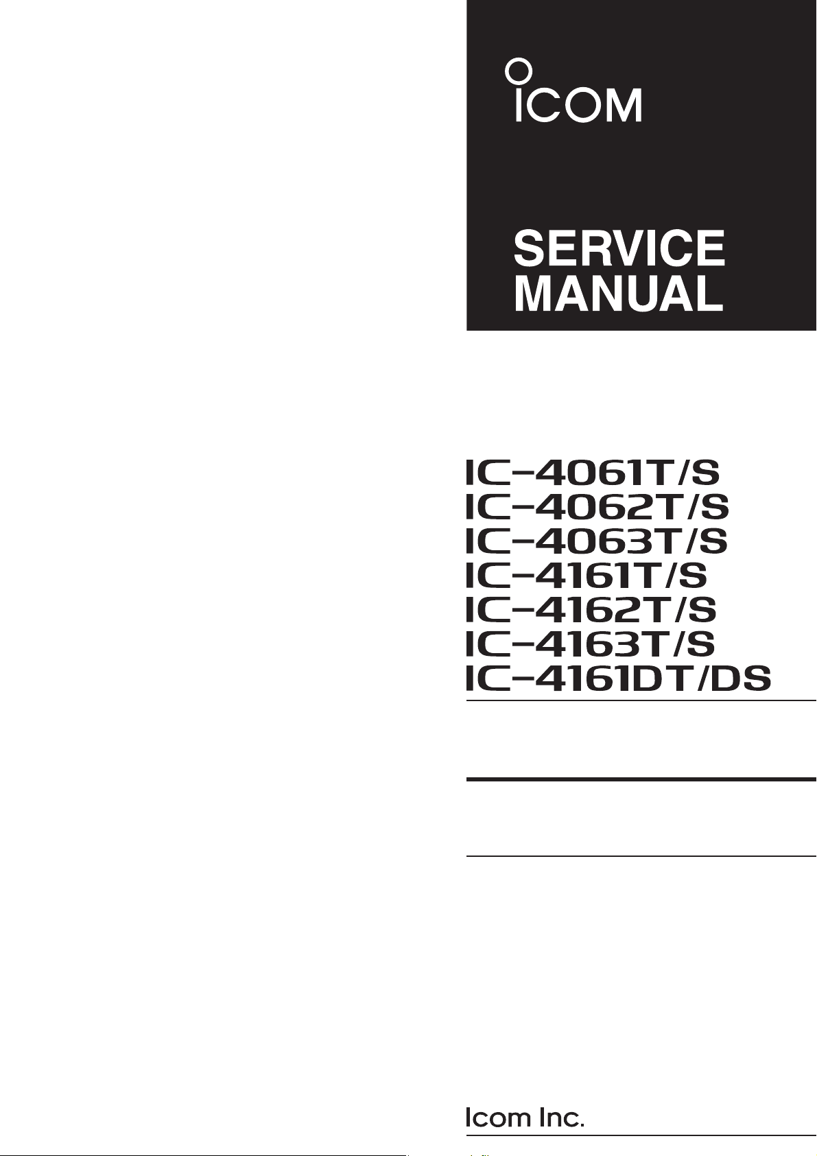
UHF TRANSCEVER
S-14229HZ-C1Jan. 2008
q
INTRODUCTION
This service manual describes the latest service information for
the IC-F4061/62/63/T/S, IC-F4161/62/63T/S/ and IC-F4161DT/DS
UHF TRANSCEVER at the time of publication.
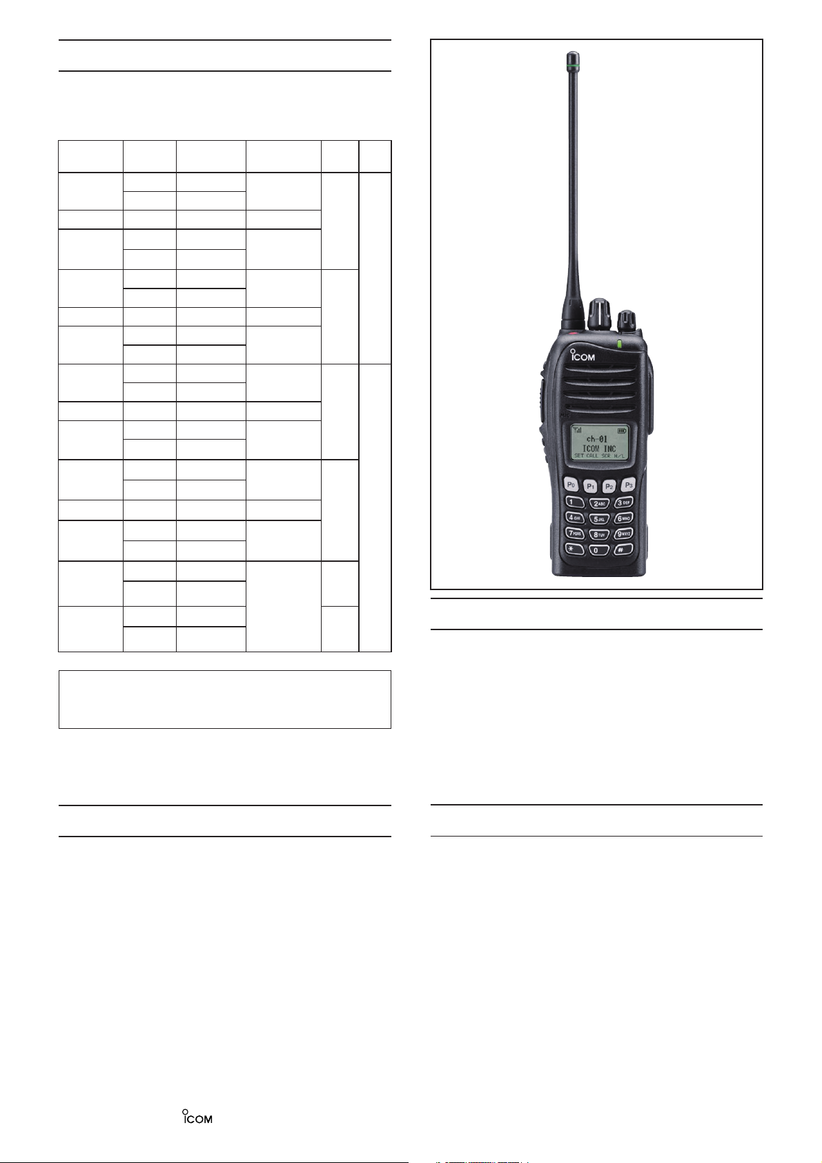
MODEL VERSION
F4061T
F4062T
F4063T
F4061S
F4062S
F4063S
F4161T
F4162T
F4163T
F4161S
F4162S
F4163S
F4161DT
(Incl.
UT-126H)
F4161DS
(Incl.
UT-126H)
USA-01 400–470
USA-02 450–512
EUR-01 400–470
GEN-01 400–470
GEN-02 450–520
USA-01 400–470
USA-02 450–512
EUR-01 400–470
GEN-01 400–470
GEN-02 450–520
USA-01 400–470
USA-02 450–512
EUR-01 400–470
GEN-01 400–470
GEN-02 450–520
USA-01 400–470
USA-02 450–512
EUR-01 400–470
GEN-01 400–470
GEN-02 450–520
USA-01 400–470
USA-02 450–512
USA-01 400–470
USA-02 450–512
FREQUENCY
RANGE (MHz)
CHANNEL
SPACING
12.5/25.0
12.5/20.0/25.0
12.5/25.0
12.5/25.0
12.5/20.0/25.0
12.5/25.0
12.5/25.0
12.5/20.0/25.0
12.5/25.0
12.5/25.0
12.5/20.0/25.0
12.5/25.0
6.25/12.5//25.0
KEY
TYPE
10-key
4-key
10-key
4-key
10-key
4-key
MDC
–
Ye s
To upgrade quality, any electrical or mechanical parts and
internal circuits are subject to change without notice or
obligation.
(IC-F4061T)
CAUTION
NEVER connect the transceiver to an AC outlet or to a DC
power supply that uses more than specifed. This will ruin
the transceiver.
DO NOT expose the transceiver to rain, snow or any liquids.
DO NOT reverse the polarities of the power supply when
connecting the transceiver.
DO NOT apply an RF signal of more than 20 dBm (100 mW) to the
antenna connector. This could damage the transceiver’s front-end.
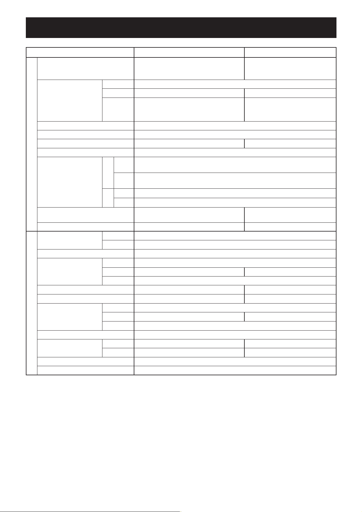
ORDERING PARTS
Be sure to include the following four points when ordering
replacement parts:
1. Make sure the problem is internal before disassembling
the transceiver.
REPAIR NOTES
2. DO NOT open the transceiver until the transceiver is
1. 10-digit Icom parts numbers
2. Component name
3. Equipment model name and unit name
4. Quantity required
disconnected from its power source.
3. DO NOT force any of the variable components. Turn
them slowly and smoothly.
4. DO NOT short any circuits or electronic parts. An
insulated tuning tool MUST be used for all adjustments.
<ORDER EXAMPLE>
1110003491 S.IC TA31136FNG IC-F4061 MAIN UNIT 5 pieces
8820001210 Screw 2438 screw IC-F4061 Top cover 10 pieces
Addresses are provided on the inside back cover for your
convenience.
5. DO NOT keep power ON for a long time when the
transceiver is defective.
6. DO NOT transmit power into a Standard Signal
Generator or a Sweep Generator.
7. ALWAYS connect a 50 dB to 60 dB attenuator between
the transceiver and a Deviation Meter or Spectrum
Analyzer when using such test equipment.
8. READ the instructions of test equipment throughly
before connecting a test equipment to the transceiver.
Icom, Icom Inc. and logo are registered trademarks of Icom Incorporated (Japan) in the United States, the United
Kingdom, Germany, France, Spain, Russia and/or other countries.

CONTENTS
SECTION 1 SPECIFICATIONS
SECTION 2 INSIDE VIEWS
SECTION 3 DISASSEMBLY INSTRUCTIONS
SECTION 4 OPTIONAL UNIT INSTALLATION
SECTION 5 CIRCUIT DESCRIPITON
5-1 RECEIVER CIRCUITS. . . . . . . . . . . . . . . . . . . . . . . . . . . . . . . . . . . . . . . . . . . . . . . . . . . . . . . . 5-1
5-2 TRANSMITTER CIRCUITS . . . . . . . . . . . . . . . . . . . . . . . . . . . . . . . . . . . . . . . . . . . . . . . . . . . . 5-2
5-3 PLL CIRCUITS. . . . . . . . . . . . . . . . . . . . . . . . . . . . . . . . . . . . . . . . . . . . . . . . . . . . . . . . . . . . . . 5-3
5-4 POWER SUPPLY CIRCUITS. . . . . . . . . . . . . . . . . . . . . . . . . . . . . . . . . . . . . . . . . . . . . . . . . . . 5-4
5-5 PORT ALLOCATIONS . . . . . . . . . . . . . . . . . . . . . . . . . . . . . . . . . . . . . . . . . . . . . . . . . . . . . . . . 5-5
SECTION 6 ADJUSTMENT PROCEDURES
6-1 PREPARATION . . . . . . . . . . . . . . . . . . . . . . . . . . . . . . . . . . . . . . . . . . . . . . . . . . . . . . . . . . . . . 6-1
6-2 FREQUENCY ADJUSTMENT . . . . . . . . . . . . . . . . . . . . . . . . . . . . . . . . . . . . . . . . . . . . . . . . . . 6-4
6-3 TRANSMIT ADJUSTMENT . . . . . . . . . . . . . . . . . . . . . . . . . . . . . . . . . . . . . . . . . . . . . . . . . . . . 6-5
6-4 RECEIVE ADJUSTMENT . . . . . . . . . . . . . . . . . . . . . . . . . . . . . . . . . . . . . . . . . . . . . . . . . . . . . 6-6
SECTION 7 PARTS LIST
SECTION 8 MECHANICAL PARTS AND DISASSEMBLY
SECTION 9 SEMICONDUCTOR INFORMATION
SECTION 10 BOARD LAYOUTS
10-1 FRONT UNIT . . . . . . . . . . . . . . . . . . . . . . . . . . . . . . . . . . . . . . . . . . . . . . . . . . . . . . . . . . . . . . . 10-1
10-2 MAIN UNIT. . . . . . . . . . . . . . . . . . . . . . . . . . . . . . . . . . . . . . . . . . . . . . . . . . . . . . . . . . . . . . . . . 10-1
10-3 RF UNIT. . . . . . . . . . . . . . . . . . . . . . . . . . . . . . . . . . . . . . . . . . . . . . . . . . . . . . . . . . . . . . . . . . . 10-1
10-4 JACK UNIT. . . . . . . . . . . . . . . . . . . . . . . . . . . . . . . . . . . . . . . . . . . . . . . . . . . . . . . . . . . . . . . . . 10-1
10-5 VR UNIT. . . . . . . . . . . . . . . . . . . . . . . . . . . . . . . . . . . . . . . . . . . . . . . . . . . . . . . . . . . . . . . . . . . 10-1
10-6 BC-160. . . . . . . . . . . . . . . . . . . . . . . . . . . . . . . . . . . . . . . . . . . . . . . . . . . . . . . . . . . . . . . . . . . . 10-1
SECTION 11 BLOCK DIAGRAM
SECTION 12 VOLTAGE DIAGRAM
SECTION 13 BC-160
SECTION 1 SPECIFICATIONS
[USA], [GEN], [EXP] [EUR]
• Frequency coverage 400–470 MHz [USA-01], [GEN-01],
450–512 MHz [USA-02]
450–520 MHz [GEN-02], [EXP-02]
• Type of emission Wide 16K0F3E (25.0 kHz)
Middle – 14K0F3E (20.0 kHz)
11K0F3E, 11K0F7E/D (15.0 kHz)
Narrow
• Number of programable channels 512 channels (128 zones)
• Antenna impedance 50 Ω (nominal)
• Operating temperature range −22˚F to +140˚F –25˚C to +55˚C
• Power supply requirement Specified Icom's battery packs only (Operatable voltage; 7.2 V DC negative ground)
GENERAL
• Current drain (approx.)
• Dimensions (with BP-232N)
(projections not included)
• Weight (with BP-232N, approx.) 12 oz 340 g
• Transmit output power High 5 W
• Modulation Variable reactance frequency modulation
• Max. frequency deviation Wide
• Frequency error ±1.0 ppm ±1.5 kHz
• Spurious emission
• Adjacent channel power Wide
TRANSMITTER
• Audio harmonic distortion 3% typ. (with 1 kHz AF 40% deviation)
• FM hum and noise
(without CCITT filter)
• Limiting charact of modulation 60–100% of max. deviation
• Microphone impedance 2.2 k
*; Available when an optional digital unit (UT-119H/UT-126H) is installed.
Stand-
by
RX
Max.
audio
at 5 W 1.8 A
TX
at 1 W 0.7 A
Low 1 W
Middle – ±4.0 kHz
Narrow ±2.5 kHz
Middle
Narrow More than 60 dB (70 dB typ.)
Wide More than 40 dB (46 dB typ.) –
Narrow More than 34 dB (40 dB typ.) –
8K50F3E, 8K10F1E/D (12.5 kHz)
4K00F1E/D (6.25 kHz)*
100 mA
140 mA (with UT-119H/UT-126H)
600 mA
3
2
/32 (W) × 5 11/32 (H) × 1 17/32 (D) in 53.0 (W) × 136.0 (H) × 38.5 (D) mm
±5.0 kHz
75 dB typ. 0.25 μW (≤1 GHz), 1.00 μW (>1 GHz)
More than 70 dB (80 dB typ.)
– More than 70 dB (80 dB typ.)
Ω
400–470 MHz
8K50F3E (12.5 kHz)
4K00F1E/D (6.25 kHz)*
1 - 1

[USA], [GEN], [EXP] [EUR]
• Receive system Double conversion superheterodyne
• Intermediate frequencies 1st IF; 46.35 MHz, 2nd IF; 450 kHz
• Sensitivity 0.25 μV typ. at 12 dB SINAD −4 dBμV (EMF) typ. at 20 dB SINAD
• Squelch sensitivity (at threshold) 0.25 μV typ.
• Adjacent Frequency
selectivity
• Spurious response More than 70 dB (80 dB typ.)
• Intermodulation More than 70 dB (74 dB typ.) More than 65 dB (67 dB typ.)
• Hum and Noise
RECEIVER
(without CCITT filter)
• Residual modulation
(with CCITT filter)
• Audio output power 0.5 W typ. at 5% distortion with an 8 Ω load
• Audio output impedance 8
Measurements made in accordance with EIA-152-C/204D, TIA-603 ([USA], [GEN], [EXP]) or
All stated specifications are subject to change without notice or obligation.
Wide More than 70 dB (75 dB typ.)
Middle − More than 70 dB (75 dB typ.)
Narrow More than 65 dB (68 dB typ.)
Wide More than 40 dB (46 dB typ.) −
Narrow More than 34 dB (40 dB typ.) −
Wide − More than 45 dB (55 dB typ.)
Middle − More than 43 dB (53 dB typ.)
Narrow − More than 40 dB (50 dB typ.)
Ω
EN 300 086 ([EUR-01]).
1 - 2
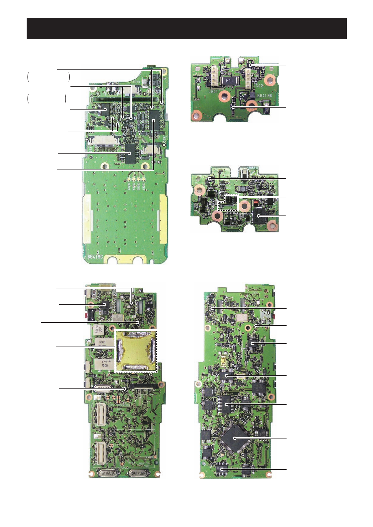
SECTION 2 INSIDE VIEWS
• FRONT UNIT
Mic selector
Q506: UNR9113J
Q516: UNR9213J
AF power amplifier
controller
Q501: 2SB1132
Q502: XP6501
AF power amplifier
(IC508: TDA8547TS)
Speaker selector
(Q512, Q513: UNR9213J)
Expander IC
(IC506: M62320FP)
Expander IC
(IC505: M62320FP)
• RF UNIT (TOP VIEW)
APC amplifier
(IC601: TA75S01F)
TX power detector
(D604: RB706F-40)
• RF UNIT (BOTTOM VIEW)
TX power detector
(D607: RB706F-40)
TX/RX antenna
switching circuit
(D601-D603: 1SV307)
TX power amplifier
(Q601: RD07MVS1)
• MAIN UNIT (TOP VIEW)
RF amplifier
(Q10: 3SK293)
D/A converter
(IC20: M62334FP)
Mixer
(Q9: 3SK324)
VCO circuits
ALC amplifier
(IC15: AN6123MS)
• MAIN UNIT (BOTTOM VIEW)
CPU 5V regulator
(IC6: NJM2870)
1st IF amplifier
(Q25: 2SC4215)
FM IF IC
(IC3: TA31136FNG)
PLL IC
(IC1: LMX2352TM)
D/A converter
(IC4: M62364FP)
CPU
(IC18: HD64F2268TF20V)
2 - 1
DTMF decoder
(IC10: BU8872FS)
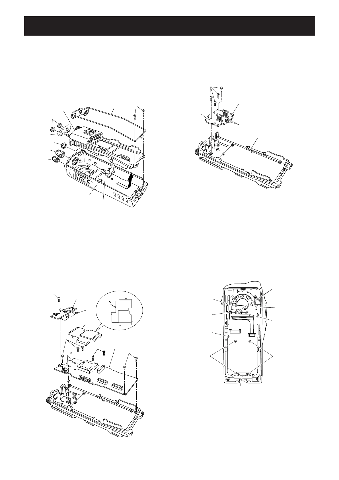
SECTION 3 DISASSEMBLY INSTRUCTION
• REMOVING THE CHASSIS UNIT
Unscrew 1 nut A, and remove 2 knobs B and C.
1
2 Unscrew 2 screws D.
3 Take off the chassis unit in the direction of the arrow.
4 Disconnect the flat cable E form J501.
5 Remove the seal F.
6 Unscrew 2 nuts G and remove the plate H.
Chassis unit
F
D
G
H
A
B
C
J501
E
• REMOVING THE RF UNIT
Unsolder 3 points A.
1
2 Unscrew 4 screws B and remove the RF unit from the
chassis.
B
RF unit
A
A
Chassis
• REMOVING THE MAIN UNIT
1 Unsolder 1 point A.
2 Unscrew 1 screw B and remove the VR unit.
3 Unsolder 5 points C and remove the shield plate D.
4 Unsolder 10 points E.
5 Unscrew 7 screws F and remove the MAIN unit from the
chassis.
B
VR unit
C 5
A
D
F
MAIN unit
E
F
10
F
• REMOVING THE FRONT UNIT
1 Disconnect the flat cable A from J503.
2 Unsolder 2 points B.
3 Unscrew 6 screws C and remove the plate D and FRONT
unit.
B
A
C
C
J503
FRONT unit
C
C
D
3 - 1
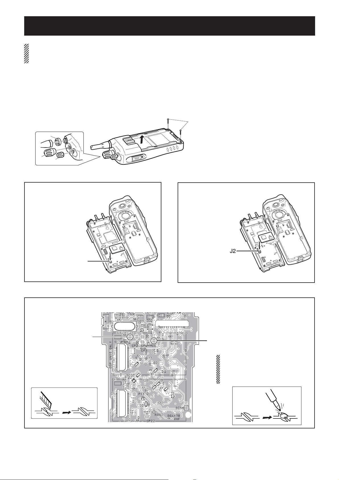
SECTION 4 OPTIONAL UNIT INSTALLATION
CAUTION! Optional unit should be installed at the authorized Icom servise center only.
The waterproof capability of the transceiver cannot be guaranteed if you install an unit yourself, or have it done at
a non-authorised dealer/service center.
Install the optional unit as follows.
Rotate [VOL] to turn the power OFF, and remove the battery pack.
q
Remove the anntena and antenna nut A.
w
Remove the rotary selector B and volume control C.
e
Unscrew two screws D, then take off the chassis from the front panel in the direction of the arrow.
r
BE CAREFUL! Flat cable is connected between the MAIN unit on the chassis and front panel.
D
A
B
C
Install the optional unit as below.
t
• UT-96R, UT-109R and UT-110R installation*
DO NOT attach the unit
to the connector "J2."
Otherwise no TX modulation or AF output is
available.
• UT-119H and UT-126H installation
DO NOT attach the unit
to the connector "J1."
Otherwise no TX modulation or AF output is
available.
J1
*; The following PC bord modifi cation is required when installing optional UT-109R and UT-110R.
Cut the pattern on the PC board at "MIC" and "AFOUT" as shown below.
AFOUT
MIC
4 - 1
NOTE: When uninstalling the unit
Be sure to re-solder the disconnected
points as below when you remove the
unit. Otherwise, no TX modulation or AF
output is available.
Re-solder
SECTION 5 CIRCUIT DESCRIPTION
5-1 RECEIVER CIRCUITS
5-1-1 ANTENNA SWITCH (MAIN and RF UNITS)
The received signals from the antenna connector are passed
through the antenna switch which toggles the receive (RX) line
and transmit (TX) line.
The received signals from the antenna connector are passed
through the low-pass fi lter (LPF; L601−L603, C601−C607), and
the antenna switch (D601, D602 and D603 are OFF).
While transmitting, the voltage on the T5V line is applied to
D601, D602 and D603, and these are ON. Thus the TX line
is connected to the antenna. Simultaneously, the RX line is
connected to the GND to prevent transmit signal entering.
While receiving, no voltage is applied to the D601, D602
and D603, and these are OFF. Thus the TX line and the
antenna is disconnected to prevent received signals entering.
Simultaneously, the RX line is disconnected from the GND and
the received signals are passed through the LPF (RF UNIT; L604,
C610, C611).
The fi ltered signals from the LPF (RF UNIT; L604, C610, C611)
are then applied to the RF circuit via the two staged tunable
bandpass fi lter (BPF; D21−D24, L31, L32, C120−C122, C125−
C127).
5-1-2 RF CIRCUIT (MAIN UNIT)
The received signals are filtered and amplified at the RF
circuit.
The fi ltered signals are applied to the RF amplifi er (Q10). The
amplifi ed signals are applied to the 1st mixer (Q9) via another twostaged BPF (D28, D29, L33, L34, C141−C144, C147, C148).
5-1-3 1st IF CIRCUITS
The received signals are converted into the 1st IF signal, and
amplified at the 1st IF circuits.
The filtered signals from the RF circuit are converted into the
46.35 MHz 1st IF signal by being mixed with the 1st Local
Oscillator (LO) signals from the VCO at the 1st mixer (Q9).
The LO signals for 435/485 MHz (Low band/High band) and lower
frequencies are generated by the RX1 VCO (Q2, D5, D6, D8), and
the LO signals for 435/485 MHz (Low band/High band) and higher
frequencies are generated by the RX2 VCO (Q1, D1, D2).
The converted 1st IF signal is passed through the 1st IF fi lter
(in wide mode; FI1, in narrow mode; FI4) via the bandwidth
switch (D34), to remove adjacent signals. The filtered signal
is applied to the 1st IF amplifi er (Q25) via another bandwidth
switch (D35). The amplifi ed 1st IF signal is then applied to the
FM IF IC (IC3, pin 16).
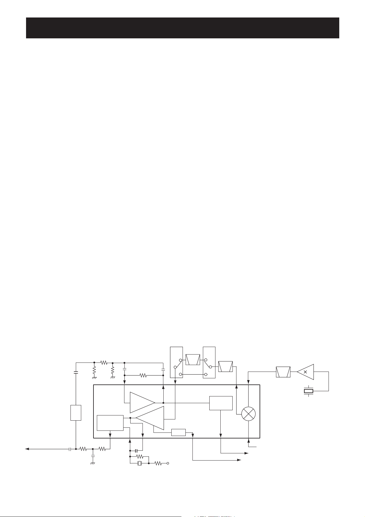
5-1-4 2nd IF AND DEMODULATOR CIRCUITS (MAIN UNIT)
The 1st IF signal is converted into the 2nd IF signal, and demodulated.
The 1st IF signal from the 1st IF amplifi er (Q25) is applied to
the 2nd IF mixer in the FM IF IC (IC3, pin 16). And the 1st IF
signal is converted into the 450 kHz 2nd IF signal by being
mixed with the 2nd LO signal from the reference frequency
oscillator (X1) via the tripler (Q18).
The converted 2nd IF signal is output from pin 3, and passed
through the 2nd IF fi lter (FI2) to suppress sideband noise. In
narrow mode, the 2nd IF signal is also passed through another
2nd IF fi lter (FI3) via bandwidth switches (D32, D33).
The fi ltered 2nd IF signal is applied to the limiter amplifi er in
the FM IF IC (IC3, pin 5). The amplifi ed 2nd IF signal is FMdemodulated at the quadrature detector (X5, IC3, pins 10, 11)
and output from pin 9. The demodulated AF signals are then
applied to the AF circuits.
5-1-5 AF CIRCUITS (FRONT and MAIN UNITS)
The demodulated AF signals from the FM IF IC are amplifi ed
and filtered at AF circuits. This transceiver employs the
base band IC for audio signal processing for both transmit
and receive. The base band IC is an audio processor and
composed of pre-amplifi er, compressor, expander, scrambler,
etc. in its package.
The demodulated AF signals from the FM IF IC (IC3, pin 9) are
applied to the base band IC (IC5, pin 23) via the Digital/Analog
switch (IC14, pins 2, 15).
The applied AF signals are amplifi ed at the amplifi er (RXA1)
and level adjusted at the volume controller (VR3), then
suppressed unwanted 3 kHz and higher audio signals at LPF.
The filtered AF signals are applied or bypassed the TX/RX
HPF, scrambler, de-emphasis sections in sequence.
• 2nd IF AND DEMODULATOR CIRCUITS
2
D/A converter
Demodulated signals
to the AF circuits
(IC4)
1
Quadrature
detector
9
8
Filter
amp.
X5
1110
Limiter
amp.
D33
N/W
SW
735
RSSI
+5V
5 - 1
12
FI3
D32
N/W
SW
FI2
Noise
detector
13
Q18
15.3 MHz
Mixer
45.9 MHz
2
BPF
FM IF IC (IC3)
16
1st IF signal from the IF amplifier (Q25)
“NOIS” signal to the CPU (IC18: pin 37)
“RSSI” signal to the CPU (IC18: pin 50)
3
X1

The TX/RX HPF filters out 250 Hz and lower audio signals,
and the de-emphasis circuit obtains –6 dB/oct of audio
characteristics. The expander expands the compressed audio
signals and also noise reduction function is provided.
The AF signals are then level adjusted at the volume controller
(VR4) and amplifi ed at the amplifi er (RXA2). The amplifi ed AF
signals are output from pin 20 and passed through another deemphasis circuit (IC13, pins 2, 15), and then applied to the D/A
converter (IC4, pin 16) for level adjustment via the AF mute
switch (IC14, pins 3, 4).
The level-adjusted AF signals are applied to the AF amplifi er
(FRONT UNIT; IC509, pin 2). The amplified AF signals are
output from pin 1, and applied to the AF power amplifier
(IC508, pin 17) to obtain 0.5 W (typical) of AF output power.
The power-amplified AF signals are output from pin 18, and
then applied to the internal speaker.
When an external speaker-microphone or headset is attached
to the multi-connector (JACK UNIT; MP801), the AF signals
from the AF amplifier (IC509, pin 1) are applied to the AF
power amplifier (IC508, pin 14). The power-amplified AF
signals are then output from pin 13, and applied to the multiconnector (JACK UNIT; MP801, pin 7).
• CTCSS/DTCS
A portion of the demodulated AF signals are passed through
the active LPF (Q28) to filters CTCSS/DTCS signal. The filtered
signal is applied to the CPU (IC18, pin 46). The CPU compares
the applied signal and the set CTCSS/DTCS, then output the
serial data to the expand IC (FRON UNIT; IC505, pin 3), and
the expand IC outputs “AFON” signal from pin 4 to the AF
power amplifi er controller (Q501, Q502, D508).
• 2/5 TONE
2/5 tone signals in the demodulated AF signals are passed
through the LPF in the base band IC (IC5) and output from
pin 21, then applied to the CPU (IC18, pin 45) and decoded.
• DTMF
DTMF signals in the demodulated AF signals are passed through
the LPF in the base band IC (IC5) and output from pin 21, then
applied to the DTMF decoder (IC10, pin 1) and decoded.
5-2 TRANSMITTER CIRCUITS
5-2-1 MICROPHONE AMPLIFIER CIRCUITS (MAIN UNIT)
The AF signals from the microphone (MIC signals) are fi ltered
and level-adjusted at microphone amplifi er circuits.
5-1-5 SQUELCH CIRCUIT
• NOISE SQUELCH
The squelch mutes the AF output signals when no RF signals
are received. By detecting noise components (30 kHz and
higher signals) in the demodulated AF signals, the squelch
circuit toggles the AF power amplifi er ON and OFF.
A portion of the demodulated AF signals from the FM IF IC
(IC3, pin 9) are applied to the D/A converter (IC4, pin 1) for
level adjustment (squelch threshold adjustment). The leveladjusted AF signals are output from pin 2 and passed through
the noise filter (IC3, pins 7, 8, R121−R124, C216−C218). The
fi ltered noise signals are amplifi ed the noise components only.
The amplifi ed noise components are converted into the pulse-type
signal at the noise detector section, and output from pin 13 as the
“NOIS” signal. The signal is applied to the CPU (IC18, pin 37).
Then the CPU outputs serial data to the expand IC (FRON UNIT;
IC505, pin 3), and the expand IC outputs “AFON” signal from pin
4 according to the “NOIS” signal level, to the AF power amplifi er
controller (FRONT UNIT; Q501, Q502, D508). The AF power
amplifier controller toggles AF power amplifier (FRONT UNIT;
IC508, IC509) ON and OFF according to the “AFON” signal.
• TONE SQUELCH
The tone squelch circuit detects tone signals and opens the
squelch only when receiving a signal containing a matched
subaudible tone. When the tone squelch is in use, and a
signal with a mismatched or no subaudible tone is received,
the tone squelch circuit mutes the AF signals even when the
noise squelch is open.
MIC signals from the microphone are passed through the
microphone switch (FRON UNIT; Q515). The microphone
switch selects the AF signals from the internal microphone
(FRON UNIT; MC501) or from an external microphone.
MIC signals from the microphone switch (FRON UNIT; Q515)
are applied to the microphone amplifi er (FRON UNIT; IC509,
pin 6), and amplified AF signals are output from pin 7, and
passed through the pre-emphasis circuit (IC13, pins 4, 5)
to obtain +6 dB/oct of frequency characteristic. The preemphasized MIC signals are then applied to the microphone
amplifi er (IC9, pin 9). And the amplifi ed MIC signals are output
from pin 8, and applied to the D/A converter (IC4, pin 9) for
level adjustment (=microphone sensitivity adjustment). The
level-adjusted MIC signals are output from pin 10, and applied
to the ALC (Automatic Level Control) circuit (IC15, pin 3)
which limits the amplitude of the MIC signals to prevent over
deviation. The amplitude-limited MIC signals are output from
pin 5, then applied to the base band IC (IC5, pin 3).
The applied MIC signals are amplifi ed at the amplifi er (TXA1),
and level adjusted at the volume controller (VR1). The level
adjusted MIC signals are applied or bypassed the compressor
section, pre-emphasis section, TX/RX HPF, de-scrambler, limiter,
splatter, in sequence, then applied to another volume controller.
The compressor compresses the MIC signals to provide high S/N
ratio for receive side, and the pre-emphasis obtains +6 dB/oct
audio characteristics. The TX/RX HPF filters out 250 Hz and
lower audio signals, the limiter limits its level and the splatter
fi lters out 3 kHz and higher audio signals.
The fi ltered MIC signals are level adjusted at another volume
controller (VR2), and then output from pin 7 via smoothing
fi lter (SMF).
• BASE BAND IC BLOCK DIAGRAM
Com-
pressor
RX
LPF
TXA1
RXA1
VR1
(HPF)
VR3
(HPF)
3TXIN
23RXIN
21SDEC
Pre-
emphasis
TX/RX
HPF
Scrambler/
De-scrambler
5 - 2
BASE BAND IC (IC5)
Limiter Splatter VR2
De-
emphasis
Expander
VR4
SMF
RXA2
7 MOD
18
19
20 SIGNAL
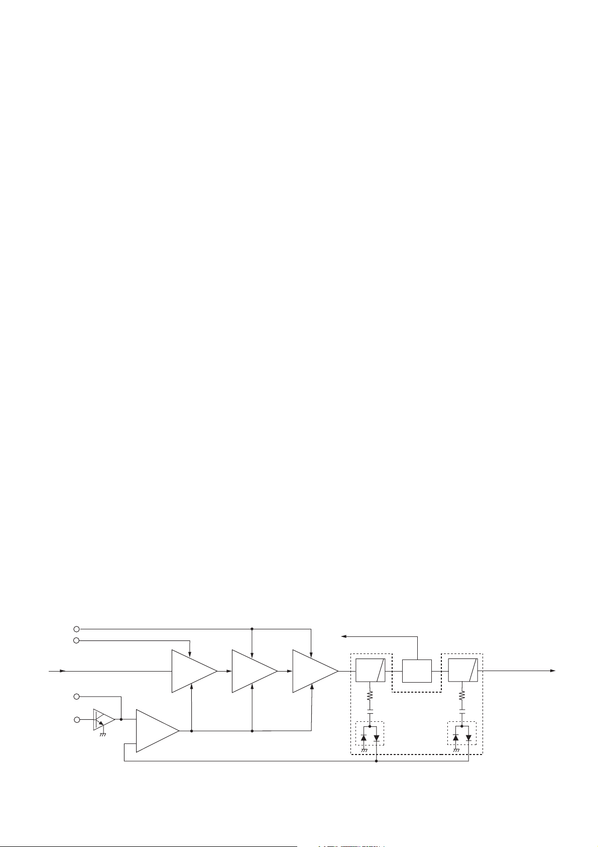
The output AF signals are then passed through the Digital/
Analog switch (IC14, pins 12, 14) and applied to the AF mixer
(IC9, pin 6) where the MIC signals and Tone signals are mixed
with (while CTCSS/DTCS are in use) via the PM/FM switch
(IC13, pins 12, 14).
The CTCSS and DTCS signals are generated by the CPU
(IC18) and output from pins 89−91. The output signals are
passed through the 3 registers (R263–R265) to change its wave
form. The wave form changed CTCSS/DTCS signals are passed
through the LPF (IC17, pins 1, 3) and the D/A converter (IC4,
pins 21, 22) for level adjustment. The level adjusted CTCSS/
DTCS signals are then applied to the AF mixer (IC9, pin 6)
2/5 tone and DTMF signals are
generated by the CPU (IC18)
.
and output from pin 43. The output signals are passed through
two LPF’s (IC17, pins 8, 10 and pins 5, 7), then applied to the AF
mixer (IC9, pin 6)
.
A portion of the transmit signal is detected by the transmit power
detector (D604, D607) to produce a DC voltage corresponding to
the transmit output power level. The detected voltage is applied
to the APC amplifier (IC601, pin 3). The transmit power setting
voltage “T2” from the D/A converter (MAIN UNIT; IC20, pin 2) is
applied to another input terminal (pin 1) as the reference voltage.
The APC amplifi er compares the detected voltage and reference
voltage, and the difference of the voltage is output from pin 4.
The output voltage controls the bias of the pre-drive (Q603),
drive (Q602) and power (Q601) amplifiers to reduce/increase
the gain of these amplifi ers for stable transmit output power.
The change of transmit output power is carried out by the
change of reference voltage “T2,” and the transmit power
muting is carried out by the TX mute switch (Q606), using the
“TMUT” signal from the CPU (IC18, pin 13).
The mixed AF signals are output from pin 7 of the AF mixer
(IC9) and passed through the D/A converter (IC4, pins 3, 4) for
level adjustment (=deviation adjustment), then applied to the
modulation circuit (D11) as the modulation signals.
The modulation signals are also applied to the reference
frequency oscillator (X1) via D/A converter (IC4, pins 11, 12)
and AF amplifi er (IC21, pins 1, 4).
5-2-2 MODULATION CIRCUIT (MAIN UNIT)
The modulation signals from the microphone amplifi er circuits
are applied to the D11, and modulate the VCO oscillating
signal by changing the reactance of D11. The modulated VCO
output signal is buffer-amplifi ed by Q4 and Q6, then applied to
transmit amplifi ers as a transmit signal via the TX/RX switch
(D14 is ON, D15 is OFF) and buffer amplifi er (Q7).
5-2-3 TRANSMIT AMPLIFIERS (RF UNIT)
The transmit signal from the buffer amplifi er (MAIN UNIT; Q7)
is amplifi ed to the transmit output level by pre-driver (Q603),
driver (Q602) and power (Q601) amplifi ers.
The power-amplifi ed transmit signal is passed through the two
staged LPF (L607, L608, C612, C616, C620, C623, C624) to
fi lter off the harmonic components in the transmit signal. The
fi ltered transmit signal is passed through the antenna switching
circuit (D601, D602 and D603 are ON), then applied to the
antenna connector (CHASSIS; J1) via another LPF (L601−
L603, C601−C607).
5-3 PLL CIRCUITS
5-5-1 VC O (Voltage Controlled Oscillator) CIRCUITS
(MAIN UNIT)
A VCO is a oscillator which its oscillating frequency is
controlled by adding voltage (lock voltage).
This transceiver has 3 VCO’s; RX VCO1 (Q1, D1, D2), RX
VCO2 (Q2, D5, D6) and TX VCO (Q3, D9, D10). The RX VCO1
oscillates the 1st LO signals for 435 MHz/485 MHz ( (Low band/
High band) and higher, and the RX VCO2 oscillates the 1st LO
signals for 435 MHz/485 MHz ( (Low band/High band) and lower
frequencies. And the TX VCO oscillates the transmit output
signal.
• RX VCO1 and RX VCO2
The RX VCO1/RX VCO2 (Q1, D1, D2/Q2, D5, D6) oscillates
the 1st LO signals. The output signals are amplified by the
buffer amplifi ers (Q4, Q6), and applied to the 1st mixer (Q37)
via TX/RX switch (D14 is OFF, D15 is ON) and LPF (L38,
C160, C161), to be mixed with the received signals to produce
the 46.35 MHz 1st IF signal.
• TX VCO
The TX VCO (Q3, D9, D10) oscillates the transmit signal. The
output signal is applied to the transmit amplifi ers via the buffer
amplifi ers (Q4, Q6) and TX/RX switch (D14 is ON, D15 is OFF).
A portion of the each VCO output is applied to the PLL IC (IC1,
pin 6) via the buffer amplifi ers (Q4, Q5) and the tunable BPF
(D16, D17, L40, C151, C152, C154).
5-2-4 APC CIRCUIT (RF UNIT)
The APC (Automatic Power Control) circuit stabilizes transmit
output power to prevent the transition of the transmit output
power level which is caused by load mismatching or heat
effect, etc. The APC circuit also selects transmit output power
from high, middle and low power.
• APC CIRCUIT
HV
T5V
from buffer amplifier (Q7)
“T2”
Q606
“TMUT”
Q603
Predrive
amp.
+
IC601
ALC
amp.
–
Q602
Drive
amp.
5-5-2 PLL CIRCUIT (MAIN UNIT)
The PLL circuit provides stable oscillation of the transmit frequency
and receive 1st LO frequency. The PLL output frequency is
controlled by the divided ratio (N-data) from the CPU.
to the receive circuits
Q601
Powe r
amp.
LPF
ANT
SW
D604
Power detecter
D607
LPF
to the anntena
5 - 3
The buffer-amplifi ed VCO output signals from the tunable BPF
(L601−L603, C601−C607) are applied to the PLL IC (IC1,
pin 6). The applied signals are divided at the prescaler and
programmable counter according to the “SSD” signal from the
CPU (IC18, pin 10). The divided signal is phase-compared with
the reference frequency signal from the reference frequency
oscillator (X1), at the phase detector.
The phase difference is output from pin 4 as a pulse type signal
after being passed through the internal charge pump. The output
signal is converted into the DC voltage (lock voltage) by passing
through the loop fi lter (R7, R8, R12, C14, C16, C19). The lock
voltage is applied to the varacter diodes (D1 and D2 of RX
VCO1, D5 and D6 of RX VCO2, D9 and D10 of TX VCO) and
locked to keep the VCO frequency constant.
• PLL CIRCUIT
If the oscillated signal drifts, its phase changes from that of
the reference frequency, causing a lock voltage change to
compensate for the drift in the VCO oscillating frequency.
RX VCO1
Q1, D1, D2
RX VCO2
Q2, D5, D6
Loop
filter
PLL unlock signal
to the CPU (IC18, pin 73)
11
4
Charge
pump
Phase
detector
TX VCO
Q3, D9, D10
Programmable
divider
Divide
ratio
adjustment
Reference
divider
Buffer
Q4
PLL IC (IC1)
Prescaler
Shift register
Buffer
Q6
Buffer
Q5
6
14
15
16
10
BPF
SCK
SSD
PLL control signals from the CPU (IC18)
PLST
15.3 MHz
reference frequency signal
D14
to transmitter circuit
D15
to 1st mixer circuit
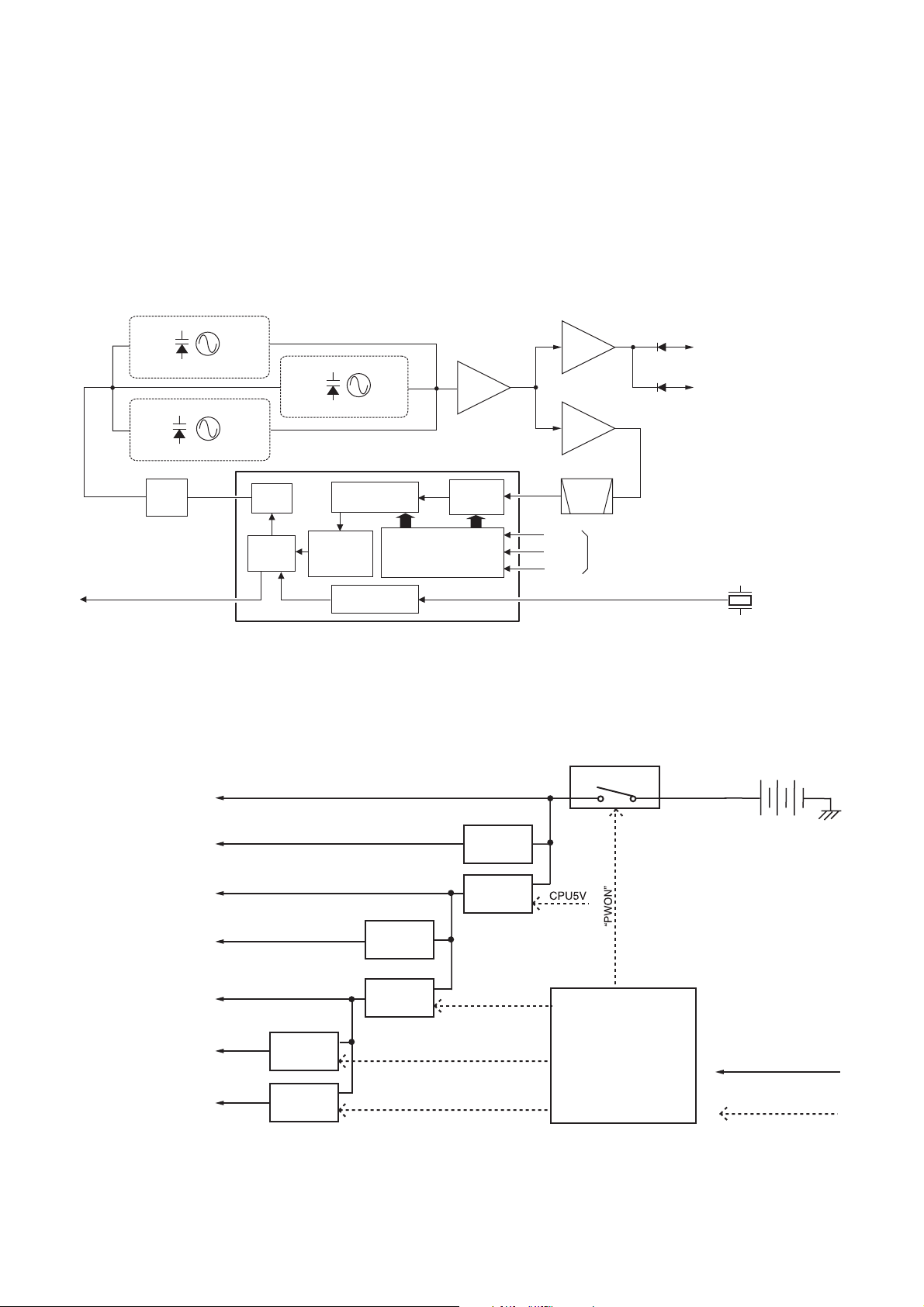
5-4 POWER SUPPLY CIRCUITS
Voltage from the attached battery pack is routed to whole of the circuit in the transceiver via switches and regulators.
Attached optional units,
AF amplifier controller
(FRONT UNIT; Q501, Q502, D508),
etc.
CPU (IC18),
EEPROM (IC19),
etc.
Attached optional units,
D/A converters,
etc.
PLL IC (IC1),
Base band IC (IC5),
etc.
VREF
IC9
VREF
regurator
CPU5V
+5V
IC6
CPU5V
regurator
+5V
regurator
Q12, Q13, Q8
VCC
Q30, Q31
Power switch
HV
Battery pack
X1
15.3 MHz
PLL IC (IC1)
Transmitter circuits
Receiver circuits
T5V
R5V
Q15
T5V
regurator
R5V
regurator
Q16
S5V
S5V
regurator
Q14
“T5C”
“R5C”
5 - 4
“S5C”
28
26
27
CPU
8
(IC18)
Voltage line
Control signal

5-5 PORT ALLOCATIONS
5-5-1 CPU (MAIN UNIT; IC18)
Pin
Port
No.
Name
1 DSDA Outputs serial data to the D/A converter (IC20, pin 6).
2 DAST Outputs strobe signal to the D/A converter (IC4, pin 6).
3 SIDE3
4−7 CBI0−3 Input ports for [ROTARY SELECTOR] (VR UNIT; S701).
10 SSO
11 SCK
13 PLST
15 DASW
17 TMUT
18 NWC2
19 NWC1
20 DDSD
21 DDAC
26 T5C
Input port for [Side3] key (S4).
“Low”=When the key is pushed.
Outputs serial data to the PLL IC (IC1, pin 15), D/A
converter (IC4, pin 8).
Outputs serial crock signal to the PLL IC (IC1, pin
14), D/A converter (IC4, pin 8).
Outputs PLL strobe signal to the PLL IC (RF UNIT;
IC1, pin 16).
Outputs mode (Digital/Analog) switching signal to
the D/A converter (IC14, pins 10, 11).
Outputs transmit mute signal to the transmit mute
switch (RF UNIT; Q606).
Outputs Narrow/Wide mode switching signal to the
bandwidth switches (Q26, D32, D33).
Outputs Narrow/Wide mode switching signal to the
bandwidth switches (Q27, Q41, Q42, D34, D35).
Outputs serial data to the DTMF decode IC (IC10,
pin 9).
Outputs serial clock signal to the DTMF decode IC
(IC10, pin 11).
Outputs T5V line control signal to the T5V regulator
(Q15).
“Low”= While transmitting.
Output R5V line control signal to the R5V regulator
27 R5C
(Q16).
“Low”= While receiving.
Output S5V line control signal to the S5V regulator
28 S5C
(Q14).
“Low”=While power save mode.
29 PTTSW
30 SIDE2
32 RMUT Outputs mute signal to the AF mute switch (D42).
37 NOIS
38 POSW
39 DDST
40 MTCK
41 PWON
Input port for [PTT] switch (S3).
“Low”=When the switch is pushed.
Input port for [Side2] key (S5).
“Low”=When the key is pushed.
Input port for the noise level from the FM IF IC (IC3,
pin 13).
Input port for power switch (VR UNIT; R702) from
power controller (D36).
Outputs strobe signal to the DTMF decode IC (MAIN
UNIT; IC10, pin 14).
Outputs serial clock signal to the base band IC
(MAIN UNIT; IC5, pin 9).
Outputs VCC line control signal to the power switch
(Q30, Q31).
“Low”=While the power is ON.
43 SENC
44 BEEP Outputs beep sound to the AF circuits (IC4, pin 13).
45 SDEC Input port for decoded 2/5 tone and DTMF signals.
46 CDEC Input port for decoded CTCSS/DTCS signal.
48 BATV Input port for remaining battery power.
49 LVIN Input port for VCO lock voltage.
50 RSSI
55 EMER Input port for [Emer] switch (VR UNIT; S702).
Outputs single tone encode signal to the LPF (IC17,
pin 10).
Input port for RSSI signal from the FM IF IC (IC3,
pin 12).
Description
Pin
Port
No.
Name
70 CSFT
71 DUSE
73 UNLK
74 RLED
75 TLED
78 FSDA
79 FSCL
81 CIRQ
88 SIDE1
CENC0−
89−
91
92 EMPH
93 MTDT Outputs serial data to the base band IC (IC5, pin 10).
96 MSCK
97 PMFM
98 ESDA Outputs serial data to the EEPROM (IC19, pin 5).
99 ESCL
100 RESL Input port for reset signal from the reset IC (IC8, pin 1).
Outputs CPU clock frequency shift signal to the CPU
clock oscillator (X2, D38).
Outputs CTCSS/DTCS select signal to the CTCSS/
DTCS switch (Q34).
Input port for PLL unlock detect signal from the PLL
IC (IC1, pin 11).
Outputs RX indicator (VR UNIT; DS701) control
signal to the LED driver (VR UNIT; Q701).
Outputs TX indicator (VR UNIT; DS701) control
signal to the LED driver (VR UNIT; Q701).
Outputs serial data to the expand IC (FRONT UNIT;
IC505, pin 3).
Outputs serial clock signal to the expand IC (FRONT
UNIT; IC505, pin 3).
Input port for external connection detect signal from
J1 and J2.
Input port for [Side1] key (S6).
“Low”=When the key is pushed.
Output CTCSS/DTCS signals to the LPF (IC17, pin 3).
2
Outputs emphasis characteristic change signal to
the D/A converter (IC13, pins 9, 10).
Outputs serial clock signal to the base band IC
(MAIN UNIT; IC5, pin 13).
Outputs modulation mode switching signal to the
PM/FM switch (IC13, pin 11) .
Outputs serial clock signal to the EEPROM (IC19,
pin 6).
Description
5-5-2 D/A CONVERTER (MAIN UNIT; IC20)
Pin
Port
No.
Name
1T1
2T2
3 TXLVA
4 RXLVA
Outputs BPF tuning voltage to the tunable BPF (
D24, L31, L32, C120−C122, C125−C127
• While receiving
Outputs BPF tuning voltage to the tunable BPF
(
D28, D29, L33, L34, C141−C144, C147).
• While transmitting
Outputs TX power setting voltage to the APC
amplifi er (RF UNIT; IC601).
Outputs oscillating frequency adjust voltage to the
TX VCO (
Outputs oscillating frequency adjust voltage to the
RX VCO1/2 (
Q3, D9, D10).
Description
D21−
).
Q1, D1, D2/Q2, D5, D6).
5-5-3 EXPAND IC (FRONT UNIT; IC505)
Pin
Port
No.
Name
4 AFON
5 LIGH
6 SPCON
7 MCON
Outputs AF power amplifi er (IC508, IC509) control
signal to the AF power amplifi er controller (Q501,
Q502, D508).
Outputs backlight control signal to the backlight
driver (Q507−Q509).
Outputs internal/external speaker select signal to
the SP/ESP switch (Q512, Q513).
Outputs internal/external microphone select signal
to the microphone controller (Q505, D504).
Description
5 - 5

SECTION 6 ADJUSTMENT PROCEDURE
6-1 PREPARATION
When adjusting IC-F4060 series, the optional CS-F3060 ADJ
(modifi ed OPC-966
▄
REQUIRED TEST EQUIPMENT
CLONING CABLE
; see illustration page 5-2) and below test equipments are required.
EQUIPMENT GRADE AND RANGE EQUIPMENT GRADE AND RANGE
FM deviation meter
Frequency counter
RF power meter
Frequency range
Measuring range
Frequency range
Frequency accuracy
Sensitivity
Measuring range
Frequency range
Impedance
SWR
: DC–600 MHz
: 0 to ±10 kHz
: 0.1–600 MHz
: ±1 ppm or better
: 100 mV or better
: 1–10 W
: 100–300 MHz
: 50
Ω
: Better than 1.2 : 1
ADJUSTMENT SOFTWARE
Attenuator
Standard signal
generator (SSG)
Oscilloscope
External speaker
(Rev. 1.1 or later), OPC-966
Power attenuation
Capacity
Frequency range
Output level
Frequency rang
Measuring range
Input impedance
Capacity
JIG CABLE
: 20 or 30 dB
: 10 W
: 0.1–600 MHz
: 0.1 µV to 32 mV
(–127 to –17 dBm)
: DC–20 MHz
: 0.01–20 V
: 8
Ω
: 1 W or more
▄
SYSTEM REQUIREMENTS
• Microsoft® Windows® 98/98SE/Me/2000/XP
• RS-232C serial port (D-sub 9 pin)
▄
ADJUSTMENYT SOFTWARE INSTALLATION
Quit all applications when Windows is running.
q
Insert the CD into the appropriate CD drive.
w
Double-click the “Setup.exe” contained in the ‘CS-F3060
e
ADJ’ folder in the CD drive.
The “Welcome to the InstallShield Wizard for CS-F3060
r
ADJ” will appear. Click [Next>].
The “Choose Destination Location” will appear. Then click
t
[Next>] to install the software to the destination folder. (e.g.
C:\Program Files\Icom\CS-F3060 ADJ)
After the installation is completed, the “InstallShield Wiz-
y
ard Complete” will appear. Then click [Finish].
Eject the CD.
u
Program group ‘CS-F3060 ADJ’ appears in the ‘Programs’
i
folder of the start menu, and ‘CS-F3060 ADJ’ icon appears on the desk top screen.
▄
BEFORE STARTING SOFTWARE ADJUSTMENT
Clone the adjustment frequencies into the transceiver, and
set the confi guration using with the CS-F3060
WARE
before starting the software adjustment. Otherwise, the
CLONING SOFT-
software adjustment can not be started.
CAUTION!: BACK UP the originally programmed mem-
ory data in the transceiver before programming the adjustment frequencies.
When program the adjustment frequencies into
the transceiver, the transceiver’s memory data
will be overwritten and lose original memory
data at the same time.
Microsoft and Windows are registered trademarks of Microsoft Corporation in the U.S.A. and other countries.
▄
STARTING SOFTWARE ADJUSTMENT
Connect the transceiver and PC with OPC-966
q
Turn the transceiver power ON.
w
Boot up Windows, and click the program group ‘CS-F3060
e
JIG CABLE
ADJ’ in the ‘Programs’ folder of the [Start] menu, then
CS-F3060 series ADJ’s window appears.
Click ‘Connect’ on the CS-F3060 ADJ’s window, then
r
appears transceiver’s up-to-date condition.
Set or modify adjustment data as specifi ed.
t
• ADJUSTMENT FREQUENCY LIST
FREQUENCY (MHz)
CH
Low band High band
1 400.000 450.000
2 435.000 485.000
3 470.000 520.000
4 434.950 484.950
5 435.000 485.000
6 435.000 485.000
7 435.000 485.000
8 400.000 450.000
9 470.000 520.000
10* 435.000 –
11* 400.000 –
12* 470.000 –
†
435.000 485.000
13
†
400.000 450.000
14
†
470.000 520.000
15
16 435.000 485.000
†
; Necessary only when the optional UT-119 is installed.
*; [EUR] only
ADJUSTMENT ITEM
TX power
Mode
TX power
Mode
TX power
Mode
TX power
Mode
TX power
Mode
TX power
Mode
TX power
Mode
TX power
Mode
TX power
Mode
TX power
Mode
TX power
Mode
TX power
Mode
TX power
Mode
TX power
Mode
TX power
Mode
TX power
Mode
CTCSS
: Low1
: Wide
: Low1
: Wdie
: Low1
: Wide
: Low1
: Wide
: High
: Wide
: Low2
: Wide
: Low1
: Wide
: Low1
: Narrow
: Low1
: Narrow
: Low1
: Middle
: Low1
: Middle
: Low1
: Middle
: Low1
: Digital
: Low1
: Digital
: Low1
: Digital
: Low1
: Wide
: 151.4 Hz:
.
6 - 1
• CONNECTION
3TANDARDSIGNALGENERATOR
§6TOM6
nD"MTOnD"M
!TTENUATOR
D"ORD"
2&POWERMETER
n77
&-
DEVIATIONMETER
/SCIILOSCOPE
#!54)/.
$/./4TRANSMITWHILE
THE33'ISCONNECTEDTO
THEANTENNACONNECTOR
&REQUENCY
COUNTER
TOTHEANTENNACONNECTOR
23#CABLE
0#
• JIG cable
)#&SERIES
/0#
#LONINGCABLE
/0#
*)'#!",%
%LECTROLYTICCAPACITOR
§&
044%
044
-)#
-)#%
30n
30
!DDAJUMPERWIREHERE
!UDIOGENERATOR
(ZTOK(Z
044
!#
MILLIVOLTMETER
n
3PEAKER
7
6 - 2
 Loading...