

Page 1
UHF TRANSCEVER
S-14229HZ-C1Jan. 2008
q
Page 2
INTRODUCTION
This service manual describes the latest service information for
the IC-F4061/62/63/T/S, IC-F4161/62/63T/S/ and IC-F4161DT/DS
UHF TRANSCEVER at the time of publication.
MODEL VERSION
F4061T
F4062T
F4063T
F4061S
F4062S
F4063S
F4161T
F4162T
F4163T
F4161S
F4162S
F4163S
F4161DT
(Incl.
UT-126H)
F4161DS
(Incl.
UT-126H)
USA-01 400–470
USA-02 450–512
EUR-01 400–470
GEN-01 400–470
GEN-02 450–520
USA-01 400–470
USA-02 450–512
EUR-01 400–470
GEN-01 400–470
GEN-02 450–520
USA-01 400–470
USA-02 450–512
EUR-01 400–470
GEN-01 400–470
GEN-02 450–520
USA-01 400–470
USA-02 450–512
EUR-01 400–470
GEN-01 400–470
GEN-02 450–520
USA-01 400–470
USA-02 450–512
USA-01 400–470
USA-02 450–512
FREQUENCY
RANGE (MHz)
CHANNEL
SPACING
12.5/25.0
12.5/20.0/25.0
12.5/25.0
12.5/25.0
12.5/20.0/25.0
12.5/25.0
12.5/25.0
12.5/20.0/25.0
12.5/25.0
12.5/25.0
12.5/20.0/25.0
12.5/25.0
6.25/12.5//25.0
KEY
TYPE
10-key
4-key
10-key
4-key
10-key
4-key
MDC
–
Ye s
To upgrade quality, any electrical or mechanical parts and
internal circuits are subject to change without notice or
obligation.
(IC-F4061T)
CAUTION
NEVER connect the transceiver to an AC outlet or to a DC
power supply that uses more than specifed. This will ruin
the transceiver.
DO NOT expose the transceiver to rain, snow or any liquids.
DO NOT reverse the polarities of the power supply when
connecting the transceiver.
DO NOT apply an RF signal of more than 20 dBm (100 mW) to the
antenna connector. This could damage the transceiver’s front-end.
ORDERING PARTS
Be sure to include the following four points when ordering
replacement parts:
1. Make sure the problem is internal before disassembling
the transceiver.
REPAIR NOTES
2. DO NOT open the transceiver until the transceiver is
1. 10-digit Icom parts numbers
2. Component name
3. Equipment model name and unit name
4. Quantity required
disconnected from its power source.
3. DO NOT force any of the variable components. Turn
them slowly and smoothly.
4. DO NOT short any circuits or electronic parts. An
insulated tuning tool MUST be used for all adjustments.
<ORDER EXAMPLE>
1110003491 S.IC TA31136FNG IC-F4061 MAIN UNIT 5 pieces
8820001210 Screw 2438 screw IC-F4061 Top cover 10 pieces
Addresses are provided on the inside back cover for your
convenience.
5. DO NOT keep power ON for a long time when the
transceiver is defective.
6. DO NOT transmit power into a Standard Signal
Generator or a Sweep Generator.
7. ALWAYS connect a 50 dB to 60 dB attenuator between
the transceiver and a Deviation Meter or Spectrum
Analyzer when using such test equipment.
8. READ the instructions of test equipment throughly
before connecting a test equipment to the transceiver.
Icom, Icom Inc. and logo are registered trademarks of Icom Incorporated (Japan) in the United States, the United
Kingdom, Germany, France, Spain, Russia and/or other countries.
Page 3

CONTENTS
SECTION 1 SPECIFICATIONS
SECTION 2 INSIDE VIEWS
SECTION 3 DISASSEMBLY INSTRUCTIONS
SECTION 4 OPTIONAL UNIT INSTALLATION
SECTION 5 CIRCUIT DESCRIPITON
5-1 RECEIVER CIRCUITS. . . . . . . . . . . . . . . . . . . . . . . . . . . . . . . . . . . . . . . . . . . . . . . . . . . . . . . . 5-1
5-2 TRANSMITTER CIRCUITS . . . . . . . . . . . . . . . . . . . . . . . . . . . . . . . . . . . . . . . . . . . . . . . . . . . . 5-2
5-3 PLL CIRCUITS. . . . . . . . . . . . . . . . . . . . . . . . . . . . . . . . . . . . . . . . . . . . . . . . . . . . . . . . . . . . . . 5-3
5-4 POWER SUPPLY CIRCUITS. . . . . . . . . . . . . . . . . . . . . . . . . . . . . . . . . . . . . . . . . . . . . . . . . . . 5-4
5-5 PORT ALLOCATIONS . . . . . . . . . . . . . . . . . . . . . . . . . . . . . . . . . . . . . . . . . . . . . . . . . . . . . . . . 5-5
SECTION 6 ADJUSTMENT PROCEDURES
6-1 PREPARATION . . . . . . . . . . . . . . . . . . . . . . . . . . . . . . . . . . . . . . . . . . . . . . . . . . . . . . . . . . . . . 6-1
6-2 FREQUENCY ADJUSTMENT . . . . . . . . . . . . . . . . . . . . . . . . . . . . . . . . . . . . . . . . . . . . . . . . . . 6-4
6-3 TRANSMIT ADJUSTMENT . . . . . . . . . . . . . . . . . . . . . . . . . . . . . . . . . . . . . . . . . . . . . . . . . . . . 6-5
6-4 RECEIVE ADJUSTMENT . . . . . . . . . . . . . . . . . . . . . . . . . . . . . . . . . . . . . . . . . . . . . . . . . . . . . 6-6
SECTION 7 PARTS LIST
SECTION 8 MECHANICAL PARTS AND DISASSEMBLY
SECTION 9 SEMICONDUCTOR INFORMATION
SECTION 10 BOARD LAYOUTS
10-1 FRONT UNIT . . . . . . . . . . . . . . . . . . . . . . . . . . . . . . . . . . . . . . . . . . . . . . . . . . . . . . . . . . . . . . . 10-1
10-2 MAIN UNIT. . . . . . . . . . . . . . . . . . . . . . . . . . . . . . . . . . . . . . . . . . . . . . . . . . . . . . . . . . . . . . . . . 10-1
10-3 RF UNIT. . . . . . . . . . . . . . . . . . . . . . . . . . . . . . . . . . . . . . . . . . . . . . . . . . . . . . . . . . . . . . . . . . . 10-1
10-4 JACK UNIT. . . . . . . . . . . . . . . . . . . . . . . . . . . . . . . . . . . . . . . . . . . . . . . . . . . . . . . . . . . . . . . . . 10-1
10-5 VR UNIT. . . . . . . . . . . . . . . . . . . . . . . . . . . . . . . . . . . . . . . . . . . . . . . . . . . . . . . . . . . . . . . . . . . 10-1
10-6 BC-160. . . . . . . . . . . . . . . . . . . . . . . . . . . . . . . . . . . . . . . . . . . . . . . . . . . . . . . . . . . . . . . . . . . . 10-1
SECTION 11 BLOCK DIAGRAM
SECTION 12 VOLTAGE DIAGRAM
SECTION 13 BC-160
Page 4
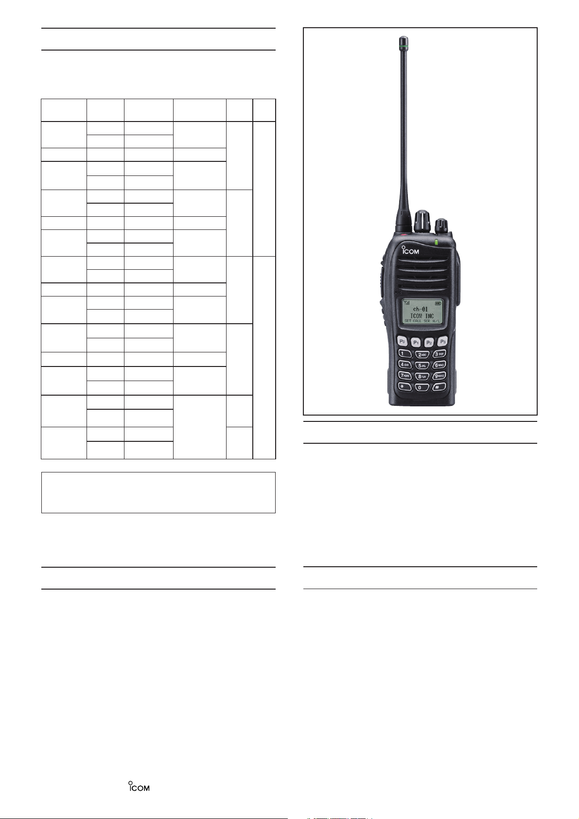
SECTION 1 SPECIFICATIONS
[USA], [GEN], [EXP] [EUR]
• Frequency coverage 400–470 MHz [USA-01], [GEN-01],
450–512 MHz [USA-02]
450–520 MHz [GEN-02], [EXP-02]
• Type of emission Wide 16K0F3E (25.0 kHz)
Middle – 14K0F3E (20.0 kHz)
11K0F3E, 11K0F7E/D (15.0 kHz)
Narrow
• Number of programable channels 512 channels (128 zones)
• Antenna impedance 50 Ω (nominal)
• Operating temperature range −22˚F to +140˚F –25˚C to +55˚C
• Power supply requirement Specified Icom's battery packs only (Operatable voltage; 7.2 V DC negative ground)
GENERAL
• Current drain (approx.)
• Dimensions (with BP-232N)
(projections not included)
• Weight (with BP-232N, approx.) 12 oz 340 g
• Transmit output power High 5 W
• Modulation Variable reactance frequency modulation
• Max. frequency deviation Wide
• Frequency error ±1.0 ppm ±1.5 kHz
• Spurious emission
• Adjacent channel power Wide
TRANSMITTER
• Audio harmonic distortion 3% typ. (with 1 kHz AF 40% deviation)
• FM hum and noise
(without CCITT filter)
• Limiting charact of modulation 60–100% of max. deviation
• Microphone impedance 2.2 k
*; Available when an optional digital unit (UT-119H/UT-126H) is installed.
Stand-
by
RX
Max.
audio
at 5 W 1.8 A
TX
at 1 W 0.7 A
Low 1 W
Middle – ±4.0 kHz
Narrow ±2.5 kHz
Middle
Narrow More than 60 dB (70 dB typ.)
Wide More than 40 dB (46 dB typ.) –
Narrow More than 34 dB (40 dB typ.) –
8K50F3E, 8K10F1E/D (12.5 kHz)
4K00F1E/D (6.25 kHz)*
100 mA
140 mA (with UT-119H/UT-126H)
600 mA
3
2
/32 (W) × 5 11/32 (H) × 1 17/32 (D) in 53.0 (W) × 136.0 (H) × 38.5 (D) mm
±5.0 kHz
75 dB typ. 0.25 μW (≤1 GHz), 1.00 μW (>1 GHz)
More than 70 dB (80 dB typ.)
– More than 70 dB (80 dB typ.)
Ω
400–470 MHz
8K50F3E (12.5 kHz)
4K00F1E/D (6.25 kHz)*
1 - 1
Page 5
[USA], [GEN], [EXP] [EUR]
• Receive system Double conversion superheterodyne
• Intermediate frequencies 1st IF; 46.35 MHz, 2nd IF; 450 kHz
• Sensitivity 0.25 μV typ. at 12 dB SINAD −4 dBμV (EMF) typ. at 20 dB SINAD
• Squelch sensitivity (at threshold) 0.25 μV typ.
• Adjacent Frequency
selectivity
• Spurious response More than 70 dB (80 dB typ.)
• Intermodulation More than 70 dB (74 dB typ.) More than 65 dB (67 dB typ.)
• Hum and Noise
RECEIVER
(without CCITT filter)
• Residual modulation
(with CCITT filter)
• Audio output power 0.5 W typ. at 5% distortion with an 8 Ω load
• Audio output impedance 8
Measurements made in accordance with EIA-152-C/204D, TIA-603 ([USA], [GEN], [EXP]) or
All stated specifications are subject to change without notice or obligation.
Wide More than 70 dB (75 dB typ.)
Middle − More than 70 dB (75 dB typ.)
Narrow More than 65 dB (68 dB typ.)
Wide More than 40 dB (46 dB typ.) −
Narrow More than 34 dB (40 dB typ.) −
Wide − More than 45 dB (55 dB typ.)
Middle − More than 43 dB (53 dB typ.)
Narrow − More than 40 dB (50 dB typ.)
Ω
EN 300 086 ([EUR-01]).
1 - 2
Page 6
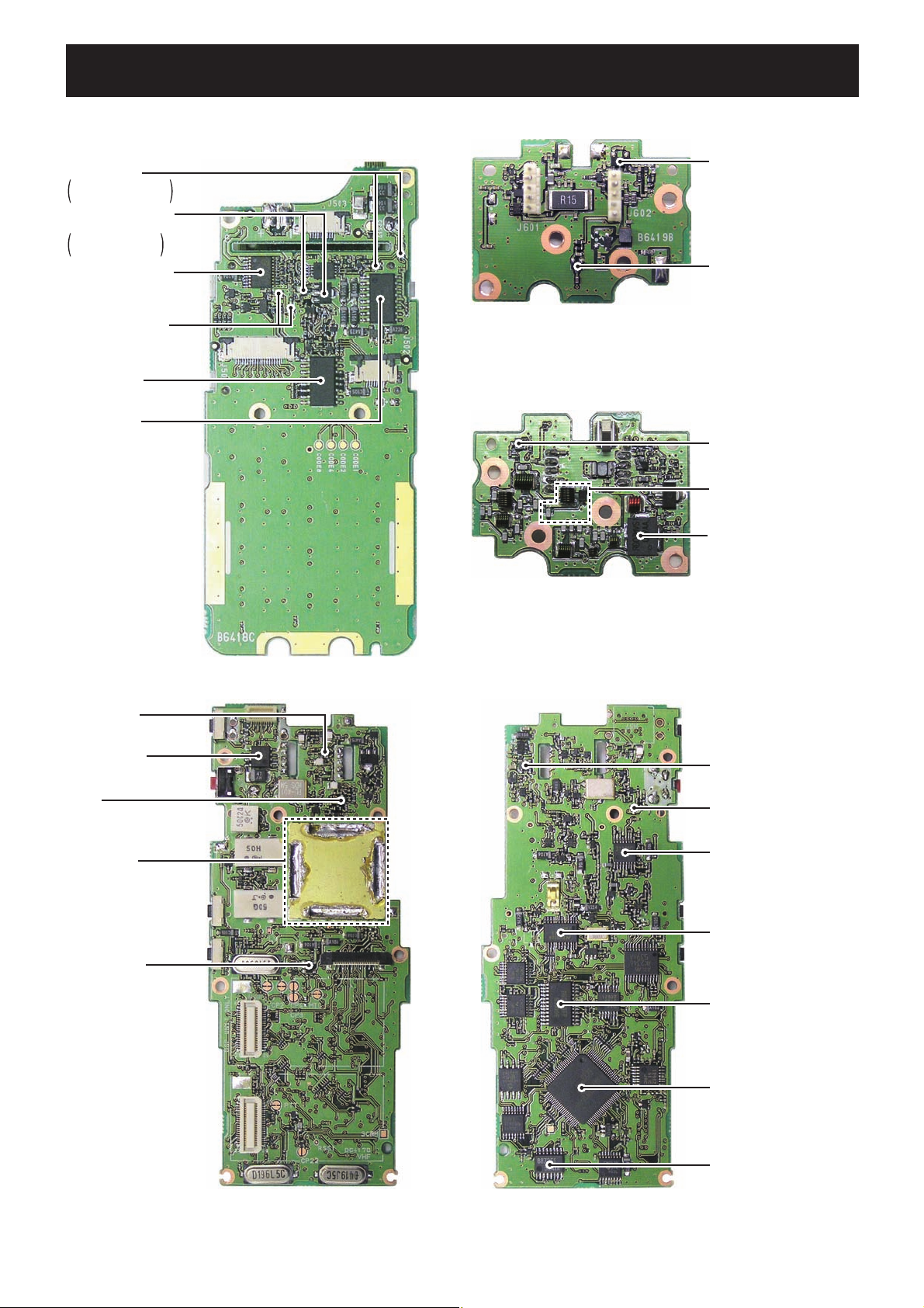
SECTION 2 INSIDE VIEWS
• FRONT UNIT
Mic selector
Q506: UNR9113J
Q516: UNR9213J
AF power amplifier
controller
Q501: 2SB1132
Q502: XP6501
AF power amplifier
(IC508: TDA8547TS)
Speaker selector
(Q512, Q513: UNR9213J)
Expander IC
(IC506: M62320FP)
Expander IC
(IC505: M62320FP)
• RF UNIT (TOP VIEW)
APC amplifier
(IC601: TA75S01F)
TX power detector
(D604: RB706F-40)
• RF UNIT (BOTTOM VIEW)
TX power detector
(D607: RB706F-40)
TX/RX antenna
switching circuit
(D601-D603: 1SV307)
TX power amplifier
(Q601: RD07MVS1)
• MAIN UNIT (TOP VIEW)
RF amplifier
(Q10: 3SK293)
D/A converter
(IC20: M62334FP)
Mixer
(Q9: 3SK324)
VCO circuits
ALC amplifier
(IC15: AN6123MS)
• MAIN UNIT (BOTTOM VIEW)
CPU 5V regulator
(IC6: NJM2870)
1st IF amplifier
(Q25: 2SC4215)
FM IF IC
(IC3: TA31136FNG)
PLL IC
(IC1: LMX2352TM)
D/A converter
(IC4: M62364FP)
CPU
(IC18: HD64F2268TF20V)
2 - 1
DTMF decoder
(IC10: BU8872FS)
Page 7
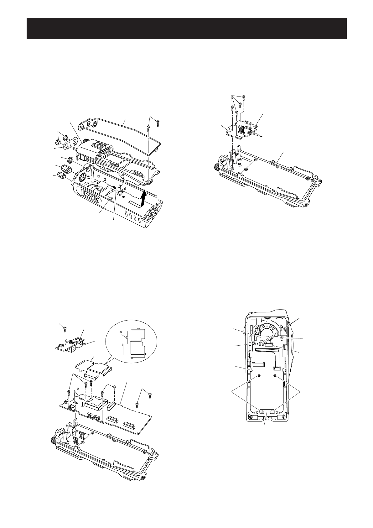
SECTION 3 DISASSEMBLY INSTRUCTION
• REMOVING THE CHASSIS UNIT
Unscrew 1 nut A, and remove 2 knobs B and C.
1
2 Unscrew 2 screws D.
3 Take off the chassis unit in the direction of the arrow.
4 Disconnect the flat cable E form J501.
5 Remove the seal F.
6 Unscrew 2 nuts G and remove the plate H.
Chassis unit
F
D
G
H
A
B
C
J501
E
• REMOVING THE RF UNIT
Unsolder 3 points A.
1
2 Unscrew 4 screws B and remove the RF unit from the
chassis.
B
RF unit
A
A
Chassis
• REMOVING THE MAIN UNIT
1 Unsolder 1 point A.
2 Unscrew 1 screw B and remove the VR unit.
3 Unsolder 5 points C and remove the shield plate D.
4 Unsolder 10 points E.
5 Unscrew 7 screws F and remove the MAIN unit from the
chassis.
B
VR unit
C 5
A
D
F
MAIN unit
E
F
10
F
• REMOVING THE FRONT UNIT
1 Disconnect the flat cable A from J503.
2 Unsolder 2 points B.
3 Unscrew 6 screws C and remove the plate D and FRONT
unit.
B
A
C
C
J503
FRONT unit
C
C
D
3 - 1
Page 8
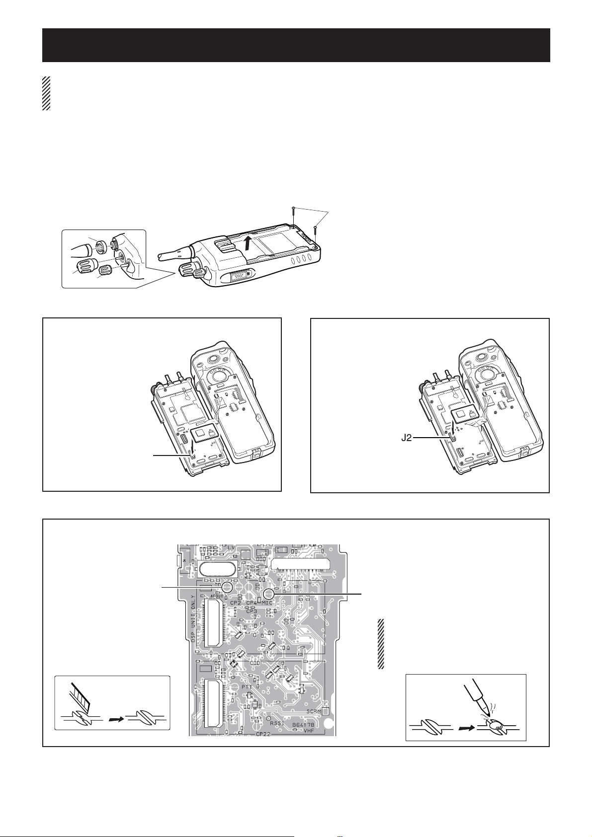
SECTION 4 OPTIONAL UNIT INSTALLATION
CAUTION! Optional unit should be installed at the authorized Icom servise center only.
The waterproof capability of the transceiver cannot be guaranteed if you install an unit yourself, or have it done at
a non-authorised dealer/service center.
Install the optional unit as follows.
Rotate [VOL] to turn the power OFF, and remove the battery pack.
q
Remove the anntena and antenna nut A.
w
Remove the rotary selector B and volume control C.
e
Unscrew two screws D, then take off the chassis from the front panel in the direction of the arrow.
r
BE CAREFUL! Flat cable is connected between the MAIN unit on the chassis and front panel.
D
A
B
C
Install the optional unit as below.
t
• UT-96R, UT-109R and UT-110R installation*
DO NOT attach the unit
to the connector "J2."
Otherwise no TX modulation or AF output is
available.
• UT-119H and UT-126H installation
DO NOT attach the unit
to the connector "J1."
Otherwise no TX modulation or AF output is
available.
J1
*; The following PC bord modifi cation is required when installing optional UT-109R and UT-110R.
Cut the pattern on the PC board at "MIC" and "AFOUT" as shown below.
AFOUT
MIC
4 - 1
NOTE: When uninstalling the unit
Be sure to re-solder the disconnected
points as below when you remove the
unit. Otherwise, no TX modulation or AF
output is available.
Re-solder
Page 9
SECTION 5 CIRCUIT DESCRIPTION
5-1 RECEIVER CIRCUITS
5-1-1 ANTENNA SWITCH (MAIN and RF UNITS)
The received signals from the antenna connector are passed
through the antenna switch which toggles the receive (RX) line
and transmit (TX) line.
The received signals from the antenna connector are passed
through the low-pass fi lter (LPF; L601−L603, C601−C607), and
the antenna switch (D601, D602 and D603 are OFF).
While transmitting, the voltage on the T5V line is applied to
D601, D602 and D603, and these are ON. Thus the TX line
is connected to the antenna. Simultaneously, the RX line is
connected to the GND to prevent transmit signal entering.
While receiving, no voltage is applied to the D601, D602
and D603, and these are OFF. Thus the TX line and the
antenna is disconnected to prevent received signals entering.
Simultaneously, the RX line is disconnected from the GND and
the received signals are passed through the LPF (RF UNIT; L604,
C610, C611).
The fi ltered signals from the LPF (RF UNIT; L604, C610, C611)
are then applied to the RF circuit via the two staged tunable
bandpass fi lter (BPF; D21−D24, L31, L32, C120−C122, C125−
C127).
5-1-2 RF CIRCUIT (MAIN UNIT)
The received signals are filtered and amplified at the RF
circuit.
The fi ltered signals are applied to the RF amplifi er (Q10). The
amplifi ed signals are applied to the 1st mixer (Q9) via another twostaged BPF (D28, D29, L33, L34, C141−C144, C147, C148).
5-1-3 1st IF CIRCUITS
The received signals are converted into the 1st IF signal, and
amplified at the 1st IF circuits.
The filtered signals from the RF circuit are converted into the
46.35 MHz 1st IF signal by being mixed with the 1st Local
Oscillator (LO) signals from the VCO at the 1st mixer (Q9).
The LO signals for 435/485 MHz (Low band/High band) and lower
frequencies are generated by the RX1 VCO (Q2, D5, D6, D8), and
the LO signals for 435/485 MHz (Low band/High band) and higher
frequencies are generated by the RX2 VCO (Q1, D1, D2).
The converted 1st IF signal is passed through the 1st IF fi lter
(in wide mode; FI1, in narrow mode; FI4) via the bandwidth
switch (D34), to remove adjacent signals. The filtered signal
is applied to the 1st IF amplifi er (Q25) via another bandwidth
switch (D35). The amplifi ed 1st IF signal is then applied to the
FM IF IC (IC3, pin 16).
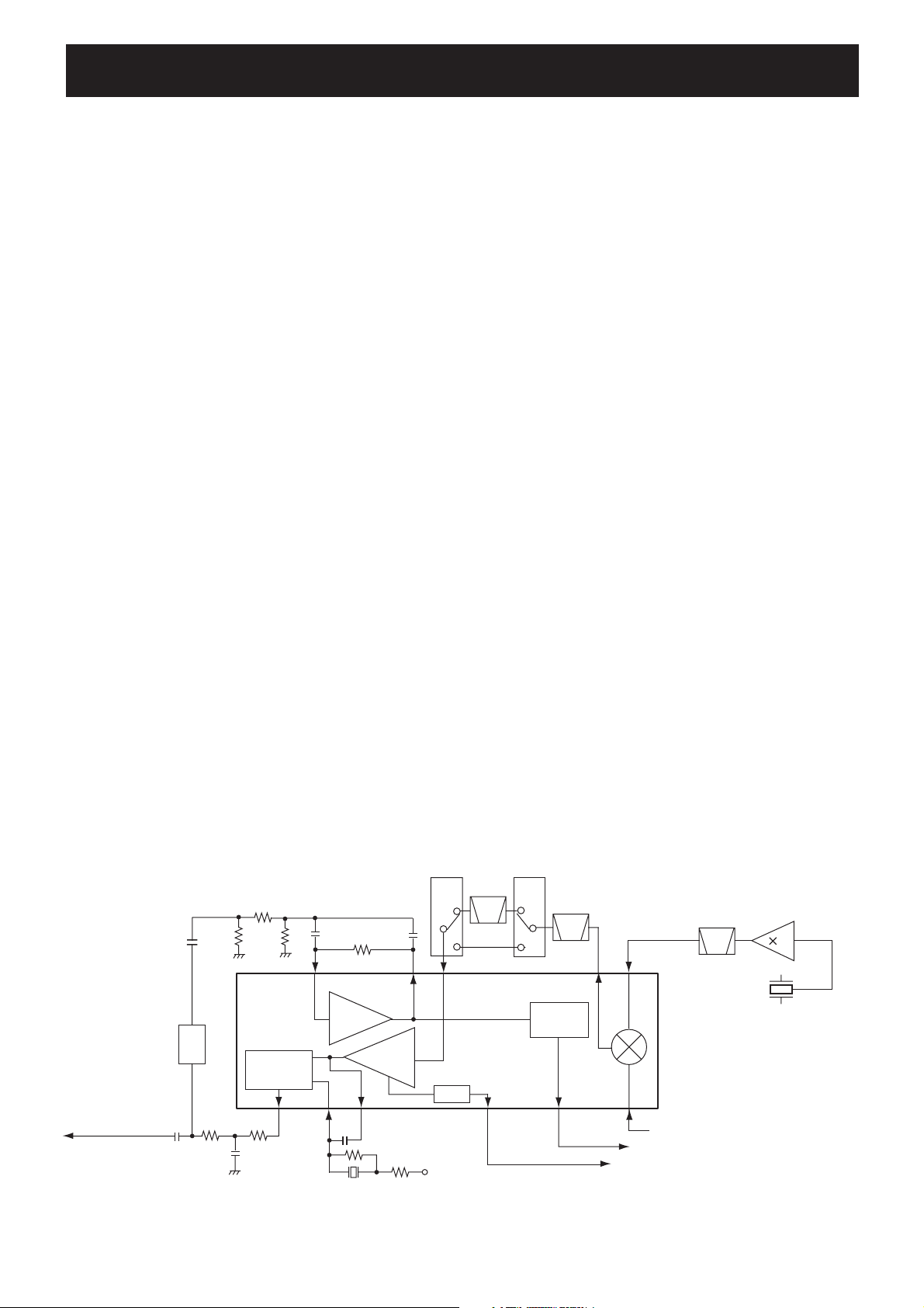
5-1-4 2nd IF AND DEMODULATOR CIRCUITS (MAIN UNIT)
The 1st IF signal is converted into the 2nd IF signal, and demodulated.
The 1st IF signal from the 1st IF amplifi er (Q25) is applied to
the 2nd IF mixer in the FM IF IC (IC3, pin 16). And the 1st IF
signal is converted into the 450 kHz 2nd IF signal by being
mixed with the 2nd LO signal from the reference frequency
oscillator (X1) via the tripler (Q18).
The converted 2nd IF signal is output from pin 3, and passed
through the 2nd IF fi lter (FI2) to suppress sideband noise. In
narrow mode, the 2nd IF signal is also passed through another
2nd IF fi lter (FI3) via bandwidth switches (D32, D33).
The fi ltered 2nd IF signal is applied to the limiter amplifi er in
the FM IF IC (IC3, pin 5). The amplifi ed 2nd IF signal is FMdemodulated at the quadrature detector (X5, IC3, pins 10, 11)
and output from pin 9. The demodulated AF signals are then
applied to the AF circuits.
5-1-5 AF CIRCUITS (FRONT and MAIN UNITS)
The demodulated AF signals from the FM IF IC are amplifi ed
and filtered at AF circuits. This transceiver employs the
base band IC for audio signal processing for both transmit
and receive. The base band IC is an audio processor and
composed of pre-amplifi er, compressor, expander, scrambler,
etc. in its package.
The demodulated AF signals from the FM IF IC (IC3, pin 9) are
applied to the base band IC (IC5, pin 23) via the Digital/Analog
switch (IC14, pins 2, 15).
The applied AF signals are amplifi ed at the amplifi er (RXA1)
and level adjusted at the volume controller (VR3), then
suppressed unwanted 3 kHz and higher audio signals at LPF.
The filtered AF signals are applied or bypassed the TX/RX
HPF, scrambler, de-emphasis sections in sequence.
• 2nd IF AND DEMODULATOR CIRCUITS
2
D/A converter
Demodulated signals
to the AF circuits
(IC4)
1
Quadrature
detector
9
8
Filter
amp.
X5
1110
Limiter
amp.
D33
N/W
SW
735
RSSI
+5V
5 - 1
12
FI3
D32
N/W
SW
FI2
Noise
detector
13
Q18
15.3 MHz
Mixer
45.9 MHz
2
BPF
FM IF IC (IC3)
16
1st IF signal from the IF amplifier (Q25)
“NOIS” signal to the CPU (IC18: pin 37)
“RSSI” signal to the CPU (IC18: pin 50)
3
X1
Page 10

The TX/RX HPF filters out 250 Hz and lower audio signals,
and the de-emphasis circuit obtains –6 dB/oct of audio
characteristics. The expander expands the compressed audio
signals and also noise reduction function is provided.
The AF signals are then level adjusted at the volume controller
(VR4) and amplifi ed at the amplifi er (RXA2). The amplifi ed AF
signals are output from pin 20 and passed through another deemphasis circuit (IC13, pins 2, 15), and then applied to the D/A
converter (IC4, pin 16) for level adjustment via the AF mute
switch (IC14, pins 3, 4).
The level-adjusted AF signals are applied to the AF amplifi er
(FRONT UNIT; IC509, pin 2). The amplified AF signals are
output from pin 1, and applied to the AF power amplifier
(IC508, pin 17) to obtain 0.5 W (typical) of AF output power.
The power-amplified AF signals are output from pin 18, and
then applied to the internal speaker.
When an external speaker-microphone or headset is attached
to the multi-connector (JACK UNIT; MP801), the AF signals
from the AF amplifier (IC509, pin 1) are applied to the AF
power amplifier (IC508, pin 14). The power-amplified AF
signals are then output from pin 13, and applied to the multiconnector (JACK UNIT; MP801, pin 7).
• CTCSS/DTCS
A portion of the demodulated AF signals are passed through
the active LPF (Q28) to filters CTCSS/DTCS signal. The filtered
signal is applied to the CPU (IC18, pin 46). The CPU compares
the applied signal and the set CTCSS/DTCS, then output the
serial data to the expand IC (FRON UNIT; IC505, pin 3), and
the expand IC outputs “AFON” signal from pin 4 to the AF
power amplifi er controller (Q501, Q502, D508).
• 2/5 TONE
2/5 tone signals in the demodulated AF signals are passed
through the LPF in the base band IC (IC5) and output from
pin 21, then applied to the CPU (IC18, pin 45) and decoded.
• DTMF
DTMF signals in the demodulated AF signals are passed through
the LPF in the base band IC (IC5) and output from pin 21, then
applied to the DTMF decoder (IC10, pin 1) and decoded.
5-2 TRANSMITTER CIRCUITS
5-2-1 MICROPHONE AMPLIFIER CIRCUITS (MAIN UNIT)
The AF signals from the microphone (MIC signals) are fi ltered
and level-adjusted at microphone amplifi er circuits.
5-1-5 SQUELCH CIRCUIT
• NOISE SQUELCH
The squelch mutes the AF output signals when no RF signals
are received. By detecting noise components (30 kHz and
higher signals) in the demodulated AF signals, the squelch
circuit toggles the AF power amplifi er ON and OFF.
A portion of the demodulated AF signals from the FM IF IC
(IC3, pin 9) are applied to the D/A converter (IC4, pin 1) for
level adjustment (squelch threshold adjustment). The leveladjusted AF signals are output from pin 2 and passed through
the noise filter (IC3, pins 7, 8, R121−R124, C216−C218). The
fi ltered noise signals are amplifi ed the noise components only.
The amplifi ed noise components are converted into the pulse-type
signal at the noise detector section, and output from pin 13 as the
“NOIS” signal. The signal is applied to the CPU (IC18, pin 37).
Then the CPU outputs serial data to the expand IC (FRON UNIT;
IC505, pin 3), and the expand IC outputs “AFON” signal from pin
4 according to the “NOIS” signal level, to the AF power amplifi er
controller (FRONT UNIT; Q501, Q502, D508). The AF power
amplifier controller toggles AF power amplifier (FRONT UNIT;
IC508, IC509) ON and OFF according to the “AFON” signal.
• TONE SQUELCH
The tone squelch circuit detects tone signals and opens the
squelch only when receiving a signal containing a matched
subaudible tone. When the tone squelch is in use, and a
signal with a mismatched or no subaudible tone is received,
the tone squelch circuit mutes the AF signals even when the
noise squelch is open.
MIC signals from the microphone are passed through the
microphone switch (FRON UNIT; Q515). The microphone
switch selects the AF signals from the internal microphone
(FRON UNIT; MC501) or from an external microphone.
MIC signals from the microphone switch (FRON UNIT; Q515)
are applied to the microphone amplifi er (FRON UNIT; IC509,
pin 6), and amplified AF signals are output from pin 7, and
passed through the pre-emphasis circuit (IC13, pins 4, 5)
to obtain +6 dB/oct of frequency characteristic. The preemphasized MIC signals are then applied to the microphone
amplifi er (IC9, pin 9). And the amplifi ed MIC signals are output
from pin 8, and applied to the D/A converter (IC4, pin 9) for
level adjustment (=microphone sensitivity adjustment). The
level-adjusted MIC signals are output from pin 10, and applied
to the ALC (Automatic Level Control) circuit (IC15, pin 3)
which limits the amplitude of the MIC signals to prevent over
deviation. The amplitude-limited MIC signals are output from
pin 5, then applied to the base band IC (IC5, pin 3).
The applied MIC signals are amplifi ed at the amplifi er (TXA1),
and level adjusted at the volume controller (VR1). The level
adjusted MIC signals are applied or bypassed the compressor
section, pre-emphasis section, TX/RX HPF, de-scrambler, limiter,
splatter, in sequence, then applied to another volume controller.
The compressor compresses the MIC signals to provide high S/N
ratio for receive side, and the pre-emphasis obtains +6 dB/oct
audio characteristics. The TX/RX HPF filters out 250 Hz and
lower audio signals, the limiter limits its level and the splatter
fi lters out 3 kHz and higher audio signals.
The fi ltered MIC signals are level adjusted at another volume
controller (VR2), and then output from pin 7 via smoothing
fi lter (SMF).
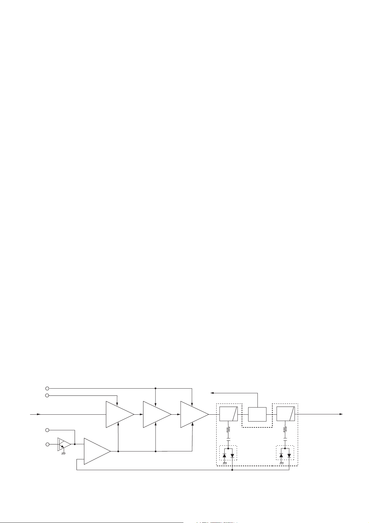
• BASE BAND IC BLOCK DIAGRAM
Com-
pressor
RX
LPF
TXA1
RXA1
VR1
(HPF)
VR3
(HPF)
3TXIN
23RXIN
21SDEC
Pre-
emphasis
TX/RX
HPF
Scrambler/
De-scrambler
5 - 2
BASE BAND IC (IC5)
Limiter Splatter VR2
De-
emphasis
Expander
VR4
SMF
RXA2
7 MOD
18
19
20 SIGNAL
Page 11
The output AF signals are then passed through the Digital/
Analog switch (IC14, pins 12, 14) and applied to the AF mixer
(IC9, pin 6) where the MIC signals and Tone signals are mixed
with (while CTCSS/DTCS are in use) via the PM/FM switch
(IC13, pins 12, 14).
The CTCSS and DTCS signals are generated by the CPU
(IC18) and output from pins 89−91. The output signals are
passed through the 3 registers (R263–R265) to change its wave
form. The wave form changed CTCSS/DTCS signals are passed
through the LPF (IC17, pins 1, 3) and the D/A converter (IC4,
pins 21, 22) for level adjustment. The level adjusted CTCSS/
DTCS signals are then applied to the AF mixer (IC9, pin 6)
2/5 tone and DTMF signals are
generated by the CPU (IC18)
.
and output from pin 43. The output signals are passed through
two LPF’s (IC17, pins 8, 10 and pins 5, 7), then applied to the AF
mixer (IC9, pin 6)
.
A portion of the transmit signal is detected by the transmit power
detector (D604, D607) to produce a DC voltage corresponding to
the transmit output power level. The detected voltage is applied
to the APC amplifier (IC601, pin 3). The transmit power setting
voltage “T2” from the D/A converter (MAIN UNIT; IC20, pin 2) is
applied to another input terminal (pin 1) as the reference voltage.
The APC amplifi er compares the detected voltage and reference
voltage, and the difference of the voltage is output from pin 4.
The output voltage controls the bias of the pre-drive (Q603),
drive (Q602) and power (Q601) amplifiers to reduce/increase
the gain of these amplifi ers for stable transmit output power.
The change of transmit output power is carried out by the
change of reference voltage “T2,” and the transmit power
muting is carried out by the TX mute switch (Q606), using the
“TMUT” signal from the CPU (IC18, pin 13).
The mixed AF signals are output from pin 7 of the AF mixer
(IC9) and passed through the D/A converter (IC4, pins 3, 4) for
level adjustment (=deviation adjustment), then applied to the
modulation circuit (D11) as the modulation signals.
The modulation signals are also applied to the reference
frequency oscillator (X1) via D/A converter (IC4, pins 11, 12)
and AF amplifi er (IC21, pins 1, 4).
5-2-2 MODULATION CIRCUIT (MAIN UNIT)
The modulation signals from the microphone amplifi er circuits
are applied to the D11, and modulate the VCO oscillating
signal by changing the reactance of D11. The modulated VCO
output signal is buffer-amplifi ed by Q4 and Q6, then applied to
transmit amplifi ers as a transmit signal via the TX/RX switch
(D14 is ON, D15 is OFF) and buffer amplifi er (Q7).
5-2-3 TRANSMIT AMPLIFIERS (RF UNIT)
The transmit signal from the buffer amplifi er (MAIN UNIT; Q7)
is amplifi ed to the transmit output level by pre-driver (Q603),
driver (Q602) and power (Q601) amplifi ers.
The power-amplifi ed transmit signal is passed through the two
staged LPF (L607, L608, C612, C616, C620, C623, C624) to
fi lter off the harmonic components in the transmit signal. The
fi ltered transmit signal is passed through the antenna switching
circuit (D601, D602 and D603 are ON), then applied to the
antenna connector (CHASSIS; J1) via another LPF (L601−
L603, C601−C607).
5-3 PLL CIRCUITS
5-5-1 VC O (Voltage Controlled Oscillator) CIRCUITS
(MAIN UNIT)
A VCO is a oscillator which its oscillating frequency is
controlled by adding voltage (lock voltage).
This transceiver has 3 VCO’s; RX VCO1 (Q1, D1, D2), RX
VCO2 (Q2, D5, D6) and TX VCO (Q3, D9, D10). The RX VCO1
oscillates the 1st LO signals for 435 MHz/485 MHz ( (Low band/
High band) and higher, and the RX VCO2 oscillates the 1st LO
signals for 435 MHz/485 MHz ( (Low band/High band) and lower
frequencies. And the TX VCO oscillates the transmit output
signal.
• RX VCO1 and RX VCO2
The RX VCO1/RX VCO2 (Q1, D1, D2/Q2, D5, D6) oscillates
the 1st LO signals. The output signals are amplified by the
buffer amplifi ers (Q4, Q6), and applied to the 1st mixer (Q37)
via TX/RX switch (D14 is OFF, D15 is ON) and LPF (L38,
C160, C161), to be mixed with the received signals to produce
the 46.35 MHz 1st IF signal.
• TX VCO
The TX VCO (Q3, D9, D10) oscillates the transmit signal. The
output signal is applied to the transmit amplifi ers via the buffer
amplifi ers (Q4, Q6) and TX/RX switch (D14 is ON, D15 is OFF).
A portion of the each VCO output is applied to the PLL IC (IC1,
pin 6) via the buffer amplifi ers (Q4, Q5) and the tunable BPF
(D16, D17, L40, C151, C152, C154).
5-2-4 APC CIRCUIT (RF UNIT)
The APC (Automatic Power Control) circuit stabilizes transmit
output power to prevent the transition of the transmit output
power level which is caused by load mismatching or heat
effect, etc. The APC circuit also selects transmit output power
from high, middle and low power.
• APC CIRCUIT
HV
T5V
from buffer amplifier (Q7)
“T2”
Q606
“TMUT”
Q603
Predrive
amp.
+
IC601
ALC
amp.
–
Q602
Drive
amp.
5-5-2 PLL CIRCUIT (MAIN UNIT)
The PLL circuit provides stable oscillation of the transmit frequency
and receive 1st LO frequency. The PLL output frequency is
controlled by the divided ratio (N-data) from the CPU.
to the receive circuits
Q601
Powe r
amp.
LPF
ANT
SW
D604
Power detecter
D607
LPF
to the anntena
5 - 3
Page 12
The buffer-amplifi ed VCO output signals from the tunable BPF
(L601−L603, C601−C607) are applied to the PLL IC (IC1,
pin 6). The applied signals are divided at the prescaler and
programmable counter according to the “SSD” signal from the
CPU (IC18, pin 10). The divided signal is phase-compared with
the reference frequency signal from the reference frequency
oscillator (X1), at the phase detector.
The phase difference is output from pin 4 as a pulse type signal
after being passed through the internal charge pump. The output
signal is converted into the DC voltage (lock voltage) by passing
through the loop fi lter (R7, R8, R12, C14, C16, C19). The lock
voltage is applied to the varacter diodes (D1 and D2 of RX
VCO1, D5 and D6 of RX VCO2, D9 and D10 of TX VCO) and
locked to keep the VCO frequency constant.
• PLL CIRCUIT
If the oscillated signal drifts, its phase changes from that of
the reference frequency, causing a lock voltage change to
compensate for the drift in the VCO oscillating frequency.
RX VCO1
Q1, D1, D2
RX VCO2
Q2, D5, D6
Loop
filter
PLL unlock signal
to the CPU (IC18, pin 73)
11
4
Charge
pump
Phase
detector
TX VCO
Q3, D9, D10
Programmable
divider
Divide
ratio
adjustment
Reference
divider
Buffer
Q4
PLL IC (IC1)
Prescaler
Shift register
Buffer
Q6
Buffer
Q5
6
14
15
16
10
BPF
SCK
SSD
PLL control signals from the CPU (IC18)
PLST
15.3 MHz
reference frequency signal
D14
to transmitter circuit
D15
to 1st mixer circuit
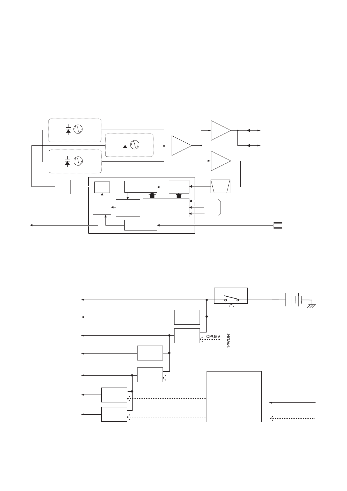
5-4 POWER SUPPLY CIRCUITS
Voltage from the attached battery pack is routed to whole of the circuit in the transceiver via switches and regulators.
Attached optional units,
AF amplifier controller
(FRONT UNIT; Q501, Q502, D508),
etc.
CPU (IC18),
EEPROM (IC19),
etc.
Attached optional units,
D/A converters,
etc.
PLL IC (IC1),
Base band IC (IC5),
etc.
VREF
IC9
VREF
regurator
CPU5V
+5V
IC6
CPU5V
regurator
+5V
regurator
Q12, Q13, Q8
VCC
Q30, Q31
Power switch
HV
Battery pack
X1
15.3 MHz
PLL IC (IC1)
Transmitter circuits
Receiver circuits
T5V
R5V
Q15
T5V
regurator
R5V
regurator
Q16
S5V
S5V
regurator
Q14
“T5C”
“R5C”
5 - 4
“S5C”
28
26
27
CPU
8
(IC18)
Voltage line
Control signal
Page 13

5-5 PORT ALLOCATIONS
5-5-1 CPU (MAIN UNIT; IC18)
Pin
Port
No.
Name
1 DSDA Outputs serial data to the D/A converter (IC20, pin 6).
2 DAST Outputs strobe signal to the D/A converter (IC4, pin 6).
3 SIDE3
4−7 CBI0−3 Input ports for [ROTARY SELECTOR] (VR UNIT; S701).
10 SSO
11 SCK
13 PLST
15 DASW
17 TMUT
18 NWC2
19 NWC1
20 DDSD
21 DDAC
26 T5C
Input port for [Side3] key (S4).
“Low”=When the key is pushed.
Outputs serial data to the PLL IC (IC1, pin 15), D/A
converter (IC4, pin 8).
Outputs serial crock signal to the PLL IC (IC1, pin
14), D/A converter (IC4, pin 8).
Outputs PLL strobe signal to the PLL IC (RF UNIT;
IC1, pin 16).
Outputs mode (Digital/Analog) switching signal to
the D/A converter (IC14, pins 10, 11).
Outputs transmit mute signal to the transmit mute
switch (RF UNIT; Q606).
Outputs Narrow/Wide mode switching signal to the
bandwidth switches (Q26, D32, D33).
Outputs Narrow/Wide mode switching signal to the
bandwidth switches (Q27, Q41, Q42, D34, D35).
Outputs serial data to the DTMF decode IC (IC10,
pin 9).
Outputs serial clock signal to the DTMF decode IC
(IC10, pin 11).
Outputs T5V line control signal to the T5V regulator
(Q15).
“Low”= While transmitting.
Output R5V line control signal to the R5V regulator
27 R5C
(Q16).
“Low”= While receiving.
Output S5V line control signal to the S5V regulator
28 S5C
(Q14).
“Low”=While power save mode.
29 PTTSW
30 SIDE2
32 RMUT Outputs mute signal to the AF mute switch (D42).
37 NOIS
38 POSW
39 DDST
40 MTCK
41 PWON
Input port for [PTT] switch (S3).
“Low”=When the switch is pushed.
Input port for [Side2] key (S5).
“Low”=When the key is pushed.
Input port for the noise level from the FM IF IC (IC3,
pin 13).
Input port for power switch (VR UNIT; R702) from
power controller (D36).
Outputs strobe signal to the DTMF decode IC (MAIN
UNIT; IC10, pin 14).
Outputs serial clock signal to the base band IC
(MAIN UNIT; IC5, pin 9).
Outputs VCC line control signal to the power switch
(Q30, Q31).
“Low”=While the power is ON.
43 SENC
44 BEEP Outputs beep sound to the AF circuits (IC4, pin 13).
45 SDEC Input port for decoded 2/5 tone and DTMF signals.
46 CDEC Input port for decoded CTCSS/DTCS signal.
48 BATV Input port for remaining battery power.
49 LVIN Input port for VCO lock voltage.
50 RSSI
55 EMER Input port for [Emer] switch (VR UNIT; S702).
Outputs single tone encode signal to the LPF (IC17,
pin 10).
Input port for RSSI signal from the FM IF IC (IC3,
pin 12).
Description
Pin
Port
No.
Name
70 CSFT
71 DUSE
73 UNLK
74 RLED
75 TLED
78 FSDA
79 FSCL
81 CIRQ
88 SIDE1
CENC0−
89−
91
92 EMPH
93 MTDT Outputs serial data to the base band IC (IC5, pin 10).
96 MSCK
97 PMFM
98 ESDA Outputs serial data to the EEPROM (IC19, pin 5).
99 ESCL
100 RESL Input port for reset signal from the reset IC (IC8, pin 1).
Outputs CPU clock frequency shift signal to the CPU
clock oscillator (X2, D38).
Outputs CTCSS/DTCS select signal to the CTCSS/
DTCS switch (Q34).
Input port for PLL unlock detect signal from the PLL
IC (IC1, pin 11).
Outputs RX indicator (VR UNIT; DS701) control
signal to the LED driver (VR UNIT; Q701).
Outputs TX indicator (VR UNIT; DS701) control
signal to the LED driver (VR UNIT; Q701).
Outputs serial data to the expand IC (FRONT UNIT;
IC505, pin 3).
Outputs serial clock signal to the expand IC (FRONT
UNIT; IC505, pin 3).
Input port for external connection detect signal from
J1 and J2.
Input port for [Side1] key (S6).
“Low”=When the key is pushed.
Output CTCSS/DTCS signals to the LPF (IC17, pin 3).
2
Outputs emphasis characteristic change signal to
the D/A converter (IC13, pins 9, 10).
Outputs serial clock signal to the base band IC
(MAIN UNIT; IC5, pin 13).
Outputs modulation mode switching signal to the
PM/FM switch (IC13, pin 11) .
Outputs serial clock signal to the EEPROM (IC19,
pin 6).
Description
5-5-2 D/A CONVERTER (MAIN UNIT; IC20)
Pin
Port
No.
Name
1T1
2T2
3 TXLVA
4 RXLVA
Outputs BPF tuning voltage to the tunable BPF (
D24, L31, L32, C120−C122, C125−C127
• While receiving
Outputs BPF tuning voltage to the tunable BPF
(
D28, D29, L33, L34, C141−C144, C147).
• While transmitting
Outputs TX power setting voltage to the APC
amplifi er (RF UNIT; IC601).
Outputs oscillating frequency adjust voltage to the
TX VCO (
Outputs oscillating frequency adjust voltage to the
RX VCO1/2 (
Q3, D9, D10).
Description
D21−
).
Q1, D1, D2/Q2, D5, D6).
5-5-3 EXPAND IC (FRONT UNIT; IC505)
Pin
Port
No.
Name
4 AFON
5 LIGH
6 SPCON
7 MCON
Outputs AF power amplifi er (IC508, IC509) control
signal to the AF power amplifi er controller (Q501,
Q502, D508).
Outputs backlight control signal to the backlight
driver (Q507−Q509).
Outputs internal/external speaker select signal to
the SP/ESP switch (Q512, Q513).
Outputs internal/external microphone select signal
to the microphone controller (Q505, D504).
Description
5 - 5
Page 14

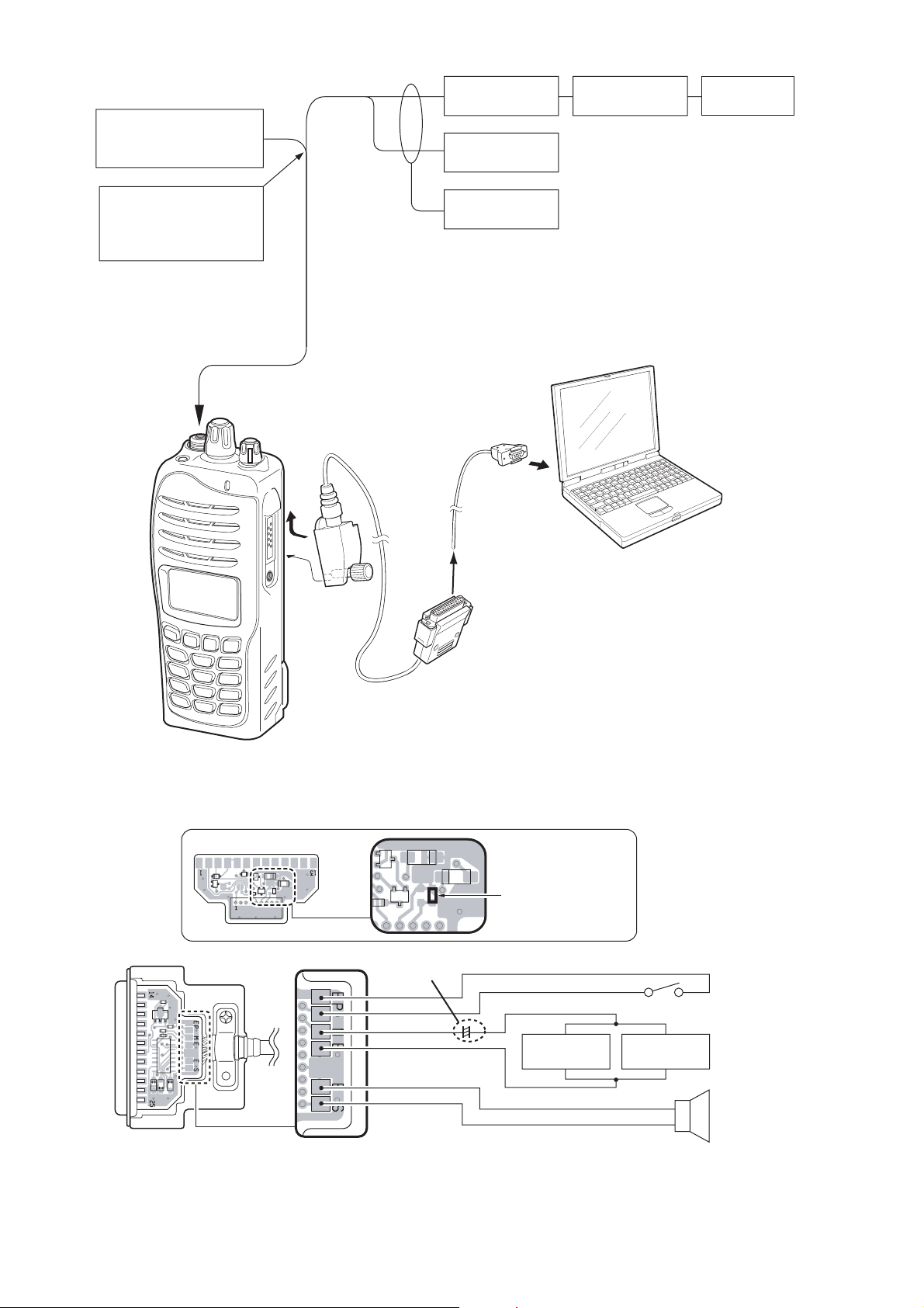
SECTION 6 ADJUSTMENT PROCEDURE
6-1 PREPARATION
When adjusting IC-F4060 series, the optional CS-F3060 ADJ
(modifi ed OPC-966
▄
REQUIRED TEST EQUIPMENT
CLONING CABLE
; see illustration page 5-2) and below test equipments are required.
EQUIPMENT GRADE AND RANGE EQUIPMENT GRADE AND RANGE
FM deviation meter
Frequency counter
RF power meter
Frequency range
Measuring range
Frequency range
Frequency accuracy
Sensitivity
Measuring range
Frequency range
Impedance
SWR
: DC–600 MHz
: 0 to ±10 kHz
: 0.1–600 MHz
: ±1 ppm or better
: 100 mV or better
: 1–10 W
: 100–300 MHz
: 50
Ω
: Better than 1.2 : 1
ADJUSTMENT SOFTWARE
Attenuator
Standard signal
generator (SSG)
Oscilloscope
External speaker
(Rev. 1.1 or later), OPC-966
Power attenuation
Capacity
Frequency range
Output level
Frequency rang
Measuring range
Input impedance
Capacity
JIG CABLE
: 20 or 30 dB
: 10 W
: 0.1–600 MHz
: 0.1 µV to 32 mV
(–127 to –17 dBm)
: DC–20 MHz
: 0.01–20 V
: 8
Ω
: 1 W or more
▄
SYSTEM REQUIREMENTS
• Microsoft® Windows® 98/98SE/Me/2000/XP
• RS-232C serial port (D-sub 9 pin)
▄
ADJUSTMENYT SOFTWARE INSTALLATION
Quit all applications when Windows is running.
q
Insert the CD into the appropriate CD drive.
w
Double-click the “Setup.exe” contained in the ‘CS-F3060
e
ADJ’ folder in the CD drive.
The “Welcome to the InstallShield Wizard for CS-F3060
r
ADJ” will appear. Click [Next>].
The “Choose Destination Location” will appear. Then click
t
[Next>] to install the software to the destination folder. (e.g.
C:\Program Files\Icom\CS-F3060 ADJ)
After the installation is completed, the “InstallShield Wiz-
y
ard Complete” will appear. Then click [Finish].
Eject the CD.
u
Program group ‘CS-F3060 ADJ’ appears in the ‘Programs’
i
folder of the start menu, and ‘CS-F3060 ADJ’ icon appears on the desk top screen.
▄
BEFORE STARTING SOFTWARE ADJUSTMENT
Clone the adjustment frequencies into the transceiver, and
set the confi guration using with the CS-F3060
WARE
before starting the software adjustment. Otherwise, the
CLONING SOFT-
software adjustment can not be started.
CAUTION!: BACK UP the originally programmed mem-
ory data in the transceiver before programming the adjustment frequencies.
When program the adjustment frequencies into
the transceiver, the transceiver’s memory data
will be overwritten and lose original memory
data at the same time.
Microsoft and Windows are registered trademarks of Microsoft Corporation in the U.S.A. and other countries.
▄
STARTING SOFTWARE ADJUSTMENT
Connect the transceiver and PC with OPC-966
q
Turn the transceiver power ON.
w
Boot up Windows, and click the program group ‘CS-F3060
e
JIG CABLE
ADJ’ in the ‘Programs’ folder of the [Start] menu, then
CS-F3060 series ADJ’s window appears.
Click ‘Connect’ on the CS-F3060 ADJ’s window, then
r
appears transceiver’s up-to-date condition.
Set or modify adjustment data as specifi ed.
t
• ADJUSTMENT FREQUENCY LIST
FREQUENCY (MHz)
CH
Low band High band
1 400.000 450.000
2 435.000 485.000
3 470.000 520.000
4 434.950 484.950
5 435.000 485.000
6 435.000 485.000
7 435.000 485.000
8 400.000 450.000
9 470.000 520.000
10* 435.000 –
11* 400.000 –
12* 470.000 –
†
435.000 485.000
13
†
400.000 450.000
14
†
470.000 520.000
15
16 435.000 485.000
†
; Necessary only when the optional UT-119 is installed.
*; [EUR] only
ADJUSTMENT ITEM
TX power
Mode
TX power
Mode
TX power
Mode
TX power
Mode
TX power
Mode
TX power
Mode
TX power
Mode
TX power
Mode
TX power
Mode
TX power
Mode
TX power
Mode
TX power
Mode
TX power
Mode
TX power
Mode
TX power
Mode
TX power
Mode
CTCSS
: Low1
: Wide
: Low1
: Wdie
: Low1
: Wide
: Low1
: Wide
: High
: Wide
: Low2
: Wide
: Low1
: Wide
: Low1
: Narrow
: Low1
: Narrow
: Low1
: Middle
: Low1
: Middle
: Low1
: Middle
: Low1
: Digital
: Low1
: Digital
: Low1
: Digital
: Low1
: Wide
: 151.4 Hz:
.
6 - 1
Page 15
• CONNECTION
3TANDARDSIGNALGENERATOR
§6TOM6
nD"MTOnD"M
!TTENUATOR
D"ORD"
2&POWERMETER
n77
&-
DEVIATIONMETER
/SCIILOSCOPE
#!54)/.
$/./4TRANSMITWHILE
THE33'ISCONNECTEDTO
THEANTENNACONNECTOR
&REQUENCY
COUNTER
TOTHEANTENNACONNECTOR
23#CABLE
0#
• JIG cable
)#&SERIES
/0#
#LONINGCABLE
/0#
*)'#!",%
%LECTROLYTICCAPACITOR
§&
044%
044
-)#
-)#%
30n
30
!DDAJUMPERWIREHERE
!UDIOGENERATOR
(ZTOK(Z
044
!#
MILLIVOLTMETER
n
3PEAKER
7
6 - 2
Page 16

• PC SCREEN EXAMPLE
!DJUSTMENTSETTING
4RANSMITOUTPUTPOWER
-ODULATIONBALANCE
-ODULATIONPRESET
#4#33$4#3DEVIATION
3QUELCH
2EFERENCEFREQUENCY
2ECEIVESENSITIVITY
28,OCKVOLTAGE,OW
28,OCKVOLTAGE(IGH
28,OCKVOLTAGEPRESET,OW
28,OCKVOLTAGEPRESET(IGH
48,OCKVOLTAGE
48,OCKVOLTAGEPRESET
3METER
&-DEVIATION.ARROW
$EVIATION-IDDLE
$EVIATION7IDE
$EVIATION$IGITAL
-ODEPRESET
;%52=ONLY
./4%
4HEABOVEVALUESFORSETTINGSAREEXAMPLEONLY
%ACHTRANSCEIVERHASITSOWNSPECIFICVALUESFOREACHSETTING
6 - 3
Page 17

6-2 FREQUENCY ADJUSTMENT
C
Select an adjustment item using [↑] / [↓] keys, then set to the specifi ed value using [←] / [→] keys on the connected PC's keyboard.
ADJUSTMENT ADJUSTMENT CONDITION
PLL LOCK
VO LTAGE
[RX LVA1]
[RX LVA2] 2 • Channel
[TX LVA] 3 • Channel
PLL LOCK
VO LTAGE
REFERENCE
FREQUENCY
[REF]
1 • Channel
• Lock voltage preset
[LV (RX1)]
• Receiving
• Lock voltage preset
[LV (RX2)]
• Receiving
• Lock voltage preset
[LV (TX)]
• Transmitting
1 • Channel
• Receiving
2 • Channel
• Receiving
3 • Channel
• Transmitting
• Channel : 3Top
• Connect an RF power meter to the
antenna connector.
• Transmitting
: 1
: 51 [1.0 V]
: 2
: 51 [1.0 V]
: 1
: 51 [1.0 V]
: 4 PC
: 3
: 3 3.2–4.4 V
UNIT OPERATION
PC
screen
screen
panel
MEASUREMENT
Click [I/O Check] in the Clone
menu to open the "I/O Check
window."
Click [Update (F5)] button, then
check the "LVIN" item on the
CS-F3060 ADJ's screen as below.
Click [Update (F5)] button, then
check the "LVIN" item on the
CS-F3060 ADJ's screen.
Loosely couple a frequency
counter to the antenna connector.
VALUE
1.00 V
3.4–4.4 V
(Verify)
(Verify)
470.000000/
512.000000 MHz
• I/O Check window
,OCKVOLTAGE
6 - 4
Page 18

6-3 TRANSMIT ADJUSTMENT
Select an adjustment item using [↑] / [↓] keys, then set to the specifi ed value using [←] / [→] keys on the connected PC's keyboard.
ADJUSTMENT ADJUSTMENT CONDITION
OUTPUT
POWER
1 • Channel
• Transmitting
: 5 Top
[Power (Hi)]
[Power (L2)] 2 • Channel
: 6 2.0 W
• Transmitting
[Power (L1)] 3 • Channel
: 2 1.0 W
• Transmitting
MODULATION
BALANCE
[BAL (Narrow)]
1 • Channel
• Preset [MOD Narrow]
: 2
: 80
• No audio applied to the JIG cable.
• Set an FM deviation meter same as;
HPF
LPF
De-emphasis
Detector
: OFF
: 20 kHz
: OFF
: (P–P)/2
• Push [P0] key while transmitting.
FM
DEVIATION
(NARROW)
[MOD N C]
• Frequency : 7
1
• Connect an audio generator to the JIG
cable and set as;
Frequency : 1.0 kHz
Level : 150 mV rms
• Set the FM deviation meter to same condi-
tion as "MODULATION BALANCE."
• Transmitting
(NARROW)
[MOD N L]
(NARROW)
[MOD N H]
(WIDE)
[MOD W C]
(WIDE)
[MOD W L]
(WIDE)
[MOD W H]
(MIDDLE)
†
[MOD M C]
(MIDDLE)
†
[MOD M L]
(MIDDLE)
†
[MOD M H]
DIGITAL
DEVIATION*
[MOD D C]
• Channel
2
• Transmitting
• Channel
3
• Transmitting
• Channel
4
• Transmitting
• Channel
5
• Transmitting
• Channel
6
• Transmitting
• Frequency
7
• Transmitting
• Frequency
8
• Transmitting
• Frequency
9
• Transmitting
• Frequency
1
• Preset [Digital Mode]
• Set the FM deviation meter to same condi-
: 8
: 9
: 2
: 1
: 3
: 10
: 11
: 12
: 13
: 7
tion as "MODULATION BALANCE."
• Transmitting
[MOD D L] 2
• Channel
: 14
• Transmitting
[MOD D H] 3
• Channel
: 15
• Transmitting
CTCSS/DTCS
DEVIATION
[CTCSS/DTCS]
• Channel
1
• CTCSS
• No audio applied to the JIG cable.
: 16
: 151.4 Hz
• Set the FM deviation meter to same condi-
tion as "MODULATION BALANCE."
• Transmitting
†
; [EUR-01] only.
*; Necessary only when the optional UT-119H or UT-126H is installed.
UNIT OPERATION
panel
Top
panel
Top
panel
Top
panel
Top
panel
MEASUREMENT
Connect an RF power meter to
the antenna connector.
Connect the FM deviation meter to the antenna connector
through an attenuator.
Connect the FM deviation meter to the antenna connector
through an attenuator.
Connect an FM deviation meter to
the antenna connector through
an attenuator.
Connect an FM deviation meter to
the antenna connector through
an attenuator.
VALUE
5.0 W
Set to square wave form
±2.05 to ±2.15 kHz
±4.05 to ±4.15 kHz
±3.2 to ±3.3 kHz
±1.35 to ±1.39 kHz
±0.68 to ±0.72 kHz
6 - 5
Page 19

6-4 RECEIVE ADJUSTMENT
Select an adjustment item using [↑] / [↓] keys, then set to the specifi ed value using [←] / [→] keys on the connected PC's keyboard.
ADJUSTMENT ADJUSTMENT CONDITION
RECEIVE
SENSITIVITY
[BPF C ALL]
NOTE:
adjusted properly.
1
"RECEIVE SENSITIVITY" must be adjusted before "S-METER." Otherwise, "S-METER" will not be
• Frequency : 1
• Connect the SSG to the antenna connector and set as;
Frequency
: 400 MHz (low band)
UNIT LOCATION
Multi
connec-
tor
450 MHz (High band)
S-METER
[RSSI]
Level
Modulation
Deviation
• Receiving
1
• Frequency : 1 Push the [ENTER] key on the connected PC's keyboard to set
• Connect the SSG to the antenna connec-
: +20 dBµ† (–87 dBm)
: 1 kHz
: ±3.5 kHz
"S3" level.
tor and set as;
Frequency
Level
Modulation
Deviation
• Receiving
2
• Set the SSG as;
Level
: 400 MHz (low band)
450 MHz (High band)
: +23 dBµ
†
(–84 dBm)
: 1 kHz
: ±3.5 kHz
: –7dBµ† (–114 dBm)
Push the [ENTER] key on the connected PC's keyboard to set
"S1" level.
• Receiving
SQUELCH
[SQL]
1 • Frequency : 1 External
• Close the squelch by adjusting the value of
speaker
[SQL] item on the CS-F3060 ADJ's screen.
• Connect the SSG to the antenna connector and set as;
Frequency
Level
Modulation
Deviation
• Receiving
†;
The output level of the standard signal generator (SSG) is indicated as the SSG's open circuit.
: 400 MHz (low band)
450 MHz (High band)
: –14 dBµ
†
(–121 dBm)
: 1 kHz
: ±3.5 kHz
MEASUREMENT
Connect the SINAD meter
with an 8 Ω load to the JIG
cable.
Connect an 8 Ω speaker to
the JIG cable.
VALUE
Minimum distortion
level
Set the [SQL] to the
value that the audio
signals just appears.
6 - 6
Page 20

SECTION 7 PARTS LIST
[FRONT UNIT] (For F4060 series)
REF ORDER
NO. NO.
IC501 1180002401 S.REG S-812C30AMC-C2K-G B 66.7/35.7
IC505 1110007330 S.IC M62320FP-DF5G B 74/36.8
IC506 1110007330 S.IC M62320FP-DF5G B 56.8/24.5
IC508 1110006770 S.IC TDA8547TS/N B 79.6/11.9
IC509 1110005330 S.IC NJM12904V-TE1 B 79.8/24.9
Q501 1520000460 S.TR 2SB1132 T100 R B 75.2/25
Q502 1590001190 S.TR XP6501-(TX) .AB B 75.8/20.8
Q506 1590003230 S.TR UNR9113J-(TX) B 83.6/41
Q507 1590003290 S.TR UNR9213J-(TX) B 72.3/6.1
Q508 1590001330 S.TR DTA114EUA T106 B 72.2/9
Q509 1590000980 S.TR DTB123EK T146 B 72.4/12.3
Q512 1590003290 S.TR UNR9213J-(TX) B 72/18
Q513 1590003290 S.TR UNR9213J-(TX) B 74.9/15.6
Q515 1560001360 S.FET 2SK3019 TL B 81/32.2
Q516 1590003290 S.TR UNR9213J-(TX) B 80.9/36
D504 1790001250 S.DIO MA2S111-(TX) B 71/25.1
D505 1160000140 S.DIO DAP222 TL B 63.6/21.9
D506 1160000140 S.DIO DAP222 TL B 63.6/26
D508 1160000060 S.DIO DAN202U T106 B 75.1/5.7
R503 7030009140 S.RES ERJ2GEJ 272 X (2.7 k) B 74/20
R504 7030008290 S.RES ERJ2GEJ 183 X (18 k) B 74.8/18.4
R505 7030005120 S.RES ERJ2GEJ 102 X (1 k) B 76.6/18.4
R506 7030005120 S.RES ERJ2GEJ 102 X (1 k) B 75.2/13.7
R508 7030005050 S.RES ERJ2GEJ 103 X (10 k) B 81.8/18.2
R509 7030005050 S.RES ERJ2GEJ 103 X (10 k) B 79.1/18.2
R510 7030005720 S.RES ERJ2GEJ 563 X (56 k) B 81.7/16.6
R511 7030005090 S.RES ERJ2GEJ 104 X (100 k) B 78.3/16.6
R513 7030005050 S.RES ERJ2GEJ 103 X (10 k) B 85.2/41.1
R514 7030005060 S.RES ERJ2GEJ 333 X (33 k) B 87.5/38.8
R515 7030005080 S.RES ERJ2GEJ 823 X (82 k) B 81.8/34
R516 7030005090 S.RES ERJ2GEJ 104 X (100 k) B 79.4/32.4
R518 7030010040 S.RES ERJ2GEJ-JPW B 66/23
R521 7030005050 S.RES ERJ2GEJ 103 X (10 k) B 68.3/24.8
R522 7030005090 S.RES ERJ2GEJ 104 X (100 k) B 53.6/18.8
R523 7030005090 S.RES ERJ2GEJ 104 X (100 k) B 54.6/18.8
R524 7030005090 S.RES ERJ2GEJ 104 X (100 k) B 55.6/18.8
R525 7030005090 S.RES ERJ2GEJ 104 X (100 k) B 56.6/18.8
R526 7030005090 S.RES ERJ2GEJ 104 X (100 k) B 65.1/23
R527 7030005090 S.RES ERJ2GEJ 104 X (100 k) B 63.6/23.5
R528 7030005090 S.RES ERJ2GEJ 104 X (100 k) B 63.6/24.4
R529 7030005090 S.RES ERJ2GEJ 104 X (100 k) B 65/24.7
R530 7030009280 S.RES ERJ2GEJ 391 X B 71.6/14.4
R531 7030005000 S.RES ERJ2GEJ 471 X (470 ) B 82.7/33
R532 7030005090 S.RES ERJ2GEJ 104 X (100 k) B 65.2/31.6
R533 7030007250 S.RES ERJ2GEJ 220 X (22 ) B 63.2/27.8
R534 7030007250 S.RES ERJ2GEJ 220 X (22 ) B 64/29.1
R535 7030004970 S.RES ERJ2GEJ 470 X (47 ) B 69.7/3.4
R536 7030004970 S.RES ERJ2GEJ 470 X (47 ) B 69.7/5.4
R537 7030005120 S.RES ERJ2GEJ 102 X (1 k) B 69.7/4.4
R538 7030005120 S.RES ERJ2GEJ 102 X (1 k) B 72/3.1
R539 7030005050 S.RES ERJ2GEJ 103 X (10 k) B 69.7/2.4
R540 7030007340 S.RES ERJ2GEJ 153 X (15 k) B 80.3/20.2
R541 7030005090 S.RES ERJ2GEJ 104 X (100 k) B 79.4/20.2
R542 7030005220 S.RES ERJ2GEJ 223 X (22 k) B 81.7/28.3
R543 7030007340 S.RES ERJ2GEJ 153 X (15 k) B 82.6/27.1
R544 7030004980 S.RES ERJ2GEJ 101 X (100 ) B 82.6/29.9
R546 7030009280 S.RES ERJ2GEJ 391 X [TENKEY] only B 71.6/15.3
R547 7030009280 S.RES ERJ2GEJ 391 X [TENKEY] only B 71.6/16.2
R548 7030005230 S.RES ERJ2GEJ 334 X (330 k) B 74.4/8.5
R552 7030005090 S.RES ERJ2GEJ 104 X (100 k) B 79.8/30.4
R553 7030005090 S.RES ERJ2GEJ 104 X (100 k)
[4-key] only B 72.9/41.7
R554 7030005090 S.RES ERJ2GEJ 104 X (100 k)
[TENKEY] only B 79.4/41.3
R555 7030005050 S.RES ERJ2GEJ 103 X (10 k) B 74.4/9.4
R557 7030004970 S.RES ERJ2GEJ 470 X (47 ) B 87/34.7
R558 7030005040 S.RES ERJ2GEJ 472 X (4.7 k) B 73.9/18.4
R559 7030005040 S.RES ERJ2GEJ 472 X (4.7 k) B 77.4/16.6
R560 7030005040 S.RES ERJ2GEJ 472 X (4.7 k) B 77.5/18.4
R561 7030005000 S.RES ERJ2GEJ 471 X (470 ) B 82.7/22.7
R562 7030005000 S.RES ERJ2GEJ 471 X (470 ) B 83.4/20.3
R563 7030005050 S.RES ERJ2GEJ 103 X (10 k) B 80.4/16.6
R564 7030005050 S.RES ERJ2GEJ 103 X (10 k) B 79.5/16.6
R566 7030010040 S.RES ERJ2GEJ-JPW B 77.6/20.2
R567 7030005090 S.RES ERJ2GEJ 104 X (100 k) B 81/30.4
C501 4550006760 S.TAN TEESVB21A336M8R B 93.4/37.3
C502 4550006760 S.TAN TEESVB21A336M8R B 96.7/37.3
C506 4550006250 S.TAN TEESVA 1A 106M8R B 75.8/31.1
C507 4550006250 S.TAN TEESVA 1A 106M8R B 70.5/29
C508 4550006250 S.TAN TEESVA 1A 106M8R B 70.5/31.1
C509 4030017460 S.CER ECJ0EB1E102K B 75.6/12.5
C510 4030016930 S.CER ECJ0EB1A104K B 73.1/20
C511 4030017460 S.CER ECJ0EB1E102K B 75.7/18.4
C514 4550006250 S.TAN TEESVA 1A 106M8R B 78.5/5.4
C515 4030016930 S.CER ECJ0EB1A104K B 80.9/18.2
C517 4030016930 S.CER ECJ0EB1A104K B 80/18.2
C518 4030017460 S.CER ECJ0EB1E102K B 71.9/26.7
C520 4030017460 S.CER ECJ0EB1E102K B 87/41.1
C522 4030016930 S.CER ECJ0EB1A104K B 85.2/39.9
C523 4030016930 S.CER ECJ0EB1A104K B 80/34
DESCRIPTION
M.
H/V
LOCATION
[FRONT UNIT] (For F4060 series)
REF ORDER
NO. NO.
C525 4030016930 S.CER ECJ0EB1A104K B 80.9/34
C526 4030017460 S.CER ECJ0EB1E102K B 70.9/26.7
C527 4030017460 S.CER ECJ0EB1E102K B 86.1/41.1
C528 4030016930 S.CER ECJ0EB1A104K B 80.3/41.3
C529 4030016930 S.CER ECJ0EB1A104K B 58/29.5
C530 4030017460 S.CER ECJ0EB1E102K B 81.2/41.3
C531 4030017460 S.CER ECJ0EB1E102K B 56.4/29.5
C532 4550007090 S.TAN TEESVA 1A 226M8R B 67.4/39.9
C534 4030016930 S.CER ECJ0EB1A104K B 65.8/38.2
C535 4030016790 S.CER ECJ0EB1C103K B 64.9/38.2
C536 4550005980 S.TAN TEESVA 1A 475M8R B 67/31.5
C537 4030016930 S.CER ECJ0EB1A104K B 55/37.7
C538 4550000460 S.TAN TEESVA 1C 105M8R B 54.6/31.9
C539 4030016930 S.CER ECJ0EB1A104K B 82.6/28.3
C540 4030018140 S.CER ECJ0EB1H391K B 81.2/20.2
C541 4030016930 S.CER ECJ0EB1A104K B 74.4/7.6
C542 4030017440 S.CER ECJ0EC1H221J B 79.8/29.4
C543 4550006250 S.TAN TEESVA 1A 106M8R B 75.8/29
C544 4030017460 S.CER ECJ0EB1E102K B 82.6/26.2
C559 4030016790 S.CER ECJ0EB1C103K T 87.8/27.1
C560 4030017770 S.CER ECJ0EB1E332K B 78.5/20.2
C561 4030016930 S.CER ECJ0EB1A104K B 82.4/31.1
J501 6510025240 S.CNR IMSA-9631S-20Y912 B 63.5/11.4
J502 6510025250 S.CNR IMSA-9631S-08Y912 B 58.8/35.5
J503 6510025260 S.CNR IMSA-9631S-10Y912 B 89.8/24.4
DS501 5040002961 S.LED SML-A12MT T86J T 82.9/33.6
DS502 5040002961 S.LED SML-A12MT T86J T 82.9/23.1
DS503 5040002961 S.LED SML-A12MT T86J T 82.9/12.6
DS504 5040002420 S.LED SML-310MT T86 T 38.1/12.9
DS505 5040002420 S.LED SML-310MT T86 T 38.1/30.9
DS506 5040002420 S.LED SML-310MT T86 [TENKEY] only T 29.2/14.9
DS507 5040002420 S.LED SML-310MT T86 [TENKEY] only T 29.2/28.9
DS508 5040002420 S.LED SML-310MT T86 [TENKEY] only T 11.7/14.9
DS509 5040002420 S.LED SML-310MT T86 [TENKEY] only T 11.7/28.9
DS510 5030002830 LCD M4-0078TAY-2
MC501 7700002760 MIC EM6027P-46C33-G-01
W501 9028930010 WIR 23/04/020/W02/W02 <TJM>
W502 9014506004 WIR 23/00/025/W02/W02 <TJM>
DESCRIPTION
M.=Mounted side (T: Mounted on the Top side, B: Mounted on the Bottom side)
7 - 1
M.
S.=Surface mount
H/V
LOCATION
Page 21

[FRONT-A UNIT] (For F4160 series)
REF ORDER
NO. NO.
IC501 1180002401 S.REG S-812C30AMC-C2K-G B 66.7/35.7
IC505 1110007330 S.IC M62320FP-DF5G B 74/36.8
IC506 1110007330 S.IC M62320FP-DF5G B 56.8/24.5
IC508 1110006770 S.IC TDA8547TS/N B 79.6/11.9
IC509 1110005330 S.IC NJM12904V-TE1 B 79.8/24.9
Q501 1520000460 S.TR 2SB1132 T100 R B 75.2/25
Q502 1590001190 S.TR XP6501-(TX) .AB B 75.8/20.8
Q506 1590003230 S.TR UNR9113J-(TX) B 83.6/41
Q507 1590003290 S.TR UNR9213J-(TX) B 72.3/6.1
Q508 1590001330 S.TR DTA114EUA T106 B 72.2/9
Q509 1590000980 S.TR DTB123EK T146 B 72.4/12.3
Q512 1590003290 S.TR UNR9213J-(TX) B 72/18
Q513 1590003290 S.TR UNR9213J-(TX) B 74.9/15.6
Q515 1560001360 S.FET 2SK3019 TL B 81/32.2
Q516 1590003290 S.TR UNR9213J-(TX) B 80.9/36
Q517 1590003290 S.TR UNR9213J-(TX) B 56.7/9
D504 1790001250 S.DIO MA2S111-(TX) B 71/25.1
D505 1160000140 S.DIO DAP222 TL B 63.6/21.9
D506 1160000140 S.DIO DAP222 TL B 63.6/26
D508 1160000060 S.DIO DAN202U T106 B 75.1/5.7
D509 1730002350 S.ZEN MA8110-M (TX) B 56.1/11.1
R503 7030009140 S.RES ERJ2GEJ 272 X (2.7 k) B 74/20
R504 7030008290 S.RES ERJ2GEJ 183 X (18 k) B 74.8/18.4
R505 7030005120 S.RES ERJ2GEJ 102 X (1 k) B 76.6/18.4
R506 7030005120 S.RES ERJ2GEJ 102 X (1 k) B 75.2/13.7
R508 7030005050 S.RES ERJ2GEJ 103 X (10 k) B 81.8/18.2
R509 7030005050 S.RES ERJ2GEJ 103 X (10 k) B 79.1/18.2
R510 7030005720 S.RES ERJ2GEJ 563 X (56 k) B 81.7/16.6
R511 7030005090 S.RES ERJ2GEJ 104 X (100 k) B 78.3/16.6
R512 7030005530 S.RES ERJ2GEJ 100 X (10 ) B 87.6/16.2
R513 7030005050 S.RES ERJ2GEJ 103 X (10 k) B 85.2/41.1
R514 7030005060 S.RES ERJ2GEJ 333 X (33 k) B 87.5/38.8
R515 7030005080 S.RES ERJ2GEJ 823 X (82 k) B 81.8/34
R516 7030005090 S.RES ERJ2GEJ 104 X (100 k) B 79.4/32.4
R521 7030005050 S.RES ERJ2GEJ 103 X (10 k) B 68.3/24.8
R522 7030005090 S.RES ERJ2GEJ 104 X (100 k) B 53.6/18.8
R523 7030005090 S.RES ERJ2GEJ 104 X (100 k) B 54.6/18.8
R524 7030005090 S.RES ERJ2GEJ 104 X (100 k) B 55.6/18.8
R525 7030005090 S.RES ERJ2GEJ 104 X (100 k) B 56.6/18.8
R526 7030005090 S.RES ERJ2GEJ 104 X (100 k) B 65.1/23
R527 7030005090 S.RES ERJ2GEJ 104 X (100 k) B 63.6/23.5
R528 7030005090 S.RES ERJ2GEJ 104 X (100 k) B 63.6/24.4
R529 7030005090 S.RES ERJ2GEJ 104 X (100 k) B 65/24.7
R530 7030009280 S.RES ERJ2GEJ 391 X B 71.6/14.4
R531 7030005000 S.RES ERJ2GEJ 471 X (470 ) B 82.7/33
R532 7030005090 S.RES ERJ2GEJ 104 X (100 k) B 65.2/31.6
R533 7030007250 S.RES ERJ2GEJ 220 X (22 ) B 63.2/27.8
R534 7030007250 S.RES ERJ2GEJ 220 X (22 ) B 64/29.1
R535 7030004970 S.RES ERJ2GEJ 470 X (47 ) B 69.7/3.4
R536 7030004970 S.RES ERJ2GEJ 470 X (47 ) B 69.7/5.4
R537 7030005120 S.RES ERJ2GEJ 102 X (1 k) B 69.7/4.4
R538 7030005120 S.RES ERJ2GEJ 102 X (1 k) B 72/3.1
R539 7030005050 S.RES ERJ2GEJ 103 X (10 k) B 69.7/2.4
R540 7030007340 S.RES ERJ2GEJ 153 X (15 k) B 80.3/20.2
R541 7030005090 S.RES ERJ2GEJ 104 X (100 k) B 79.4/20.2
R542 7030005220 S.RES ERJ2GEJ 223 X (22 k) B 81.7/28.3
R543 7030007340 S.RES ERJ2GEJ 153 X (15 k) B 82.6/27.1
R544 7030004980 S.RES ERJ2GEJ 101 X (100 ) B 82.6/29.9
R546 7030009280 S.RES ERJ2GEJ 391 X B 71.6/15.3
R547 7030009280 S.RES ERJ2GEJ 391 X [TENKEY] only B 71.6/16.2
R548 7030005230 S.RES ERJ2GEJ 334 X (330 k) B 74.4/8.5
R552 7030005090 S.RES ERJ2GEJ 104 X (100 k) B 79.8/30.4
R553 7030005090 S.RES ERJ2GEJ 104 X (100 k) B 72.9/41.7
R554 7030005090 S.RES ERJ2GEJ 104 X (100 k)
[TENKEY] only B 79.4/41.3
R555 7030005050 S.RES ERJ2GEJ 103 X (10 k) B 74.4/9.4
R557 7030005530 S.RES ERJ2GEJ 100 X (10 ) B 87/34.7
R558 7030005040 S.RES ERJ2GEJ 472 X (4.7 k) B 73.9/18.4
R559 7030005040 S.RES ERJ2GEJ 472 X (4.7 k) B 77.4/16.6
R560 7030005040 S.RES ERJ2GEJ 472 X (4.7 k) B 77.5/18.4
R561 7030005000 S.RES ERJ2GEJ 471 X (470 ) B 82.7/22.7
R562 7030005000 S.RES ERJ2GEJ 471 X (470 ) B 83.4/20.3
R563 7030005050 S.RES ERJ2GEJ 103 X (10 k) B 80.4/16.6
R564 7030005050 S.RES ERJ2GEJ 103 X (10 k) B 79.5/16.6
R566 7030010040 S.RES ERJ2GEJ-JPW B 77.6/20.2
R567 7030005090 S.RES ERJ2GEJ 104 X (100 k) B 81/30.4
R568 7030005090 S.RES ERJ2GEJ 104 X (100 k) B 69.8/42.1
R569 7030005090 S.RES ERJ2GEJ 104 X (100 k) B 70.7/42.1
R570 7030005090 S.RES ERJ2GEJ 104 X (100 k) B 71.6/42.1
R571 7030005090 S.RES ERJ2GEJ 104 X (100 k) B 57.1/7.4
R572 7030005090 S.RES ERJ2GEJ 104 X (100 k) B 69.1/20.4
C501 4550006760 S.TAN TEESVB21A336M8R B 93.4/37.3
C502 4550006760 S.TAN TEESVB21A336M8R B 96.7/37.3
C506 4550006250 S.TAN TEESVA 1A 106M8R B 75.8/31.1
C507 4550006250 S.TAN TEESVA 1A 106M8R B 70.5/29
C508 4550006250 S.TAN TEESVA 1A 106M8R B 70.5/31.1
C509 4030017460 S.CER ECJ0EB1E102K B 75.6/12.5
C510 4030016930 S.CER ECJ0EB1A104K B 73.1/20
C511 4030017460 S.CER ECJ0EB1E102K B 75.7/18.4
C514 4550006250 S.TAN TEESVA 1A 106M8R B 78.5/5.4
C515 4030016930 S.CER ECJ0EB1A104K B 80.9/18.2
C517 4030016930 S.CER ECJ0EB1A104K B 80/18.2
C518 4030017460 S.CER ECJ0EB1E102K B 71.9/26.7
C519 4030016950 S.CER ECJ0EB1A473K B 87.6/14.6
C520 4030017460 S.CER ECJ0EB1E102K B 87/41.1
C522 4030016930 S.CER ECJ0EB1A104K B 85.2/39.9
DESCRIPTION
M.
H/V
LOCATION
[FRONT-A UNIT] (For F4160 series)
REF ORDER
NO. NO.
C523 4030016930 S.CER ECJ0EB1A104K B 80/34
C525 4030016930 S.CER ECJ0EB1A104K B 80.9/34
C526 4030017460 S.CER ECJ0EB1E102K B 70.9/26.7
C527 4030017460 S.CER ECJ0EB1E102K B 86.1/41.1
C528 4030016930 S.CER ECJ0EB1A104K B 80.3/41.3
C529 4030016930 S.CER ECJ0EB1A104K B 58/29.5
C530 4030017460 S.CER ECJ0EB1E102K B 81.2/41.3
C531 4030017460 S.CER ECJ0EB1E102K B 56.4/29.5
C532 4550007090 S.TAN TEESVA 1A 226M8R B 67.4/39.9
C534 4030016930 S.CER ECJ0EB1A104K B 65.8/38.2
C535 4030016790 S.CER ECJ0EB1C103K B 64.9/38.2
C536 4550005980 S.TAN TEESVA 1A 475M8R B 67/31.5
C537 4030016930 S.CER ECJ0EB1A104K B 55/37.7
C538 4550000460 S.TAN TEESVA 1C 105M8R B 54.6/31.9
C539 4030016930 S.CER ECJ0EB1A104K B 82.6/28.3
C540 4030018140 S.CER ECJ0EB1H391K B 81.2/20.2
C541 4030016930 S.CER ECJ0EB1A104K B 74.4/7.6
C542 4030017440 S.CER ECJ0EC1H221J B 79.8/29.4
C543 4550006250 S.TAN TEESVA 1A 106M8R B 75.8/29
C544 4030017460 S.CER ECJ0EB1E102K B 82.6/26.2
C551 4030017420 S.CER ECJ0EC1H470J T 87.9/24.4
C552 4030017420 S.CER ECJ0EC1H470J T 87.9/23.5
C554 4030017420 S.CER ECJ0EC1H470J T 87.9/21.7
C556 4030017420 S.CER ECJ0EC1H470J T 87.9/25.3
C558 4030017420 S.CER ECJ0EC1H470J T 87.8/28
C559 4030016790 S.CER ECJ0EB1C103K T 87.8/27.1
C560 4030017770 S.CER ECJ0EB1E332K B 78.5/20.2
C561 4030016930 S.CER ECJ0EB1A104K B 82.4/31.1
C562 4030017460 S.CER ECJ0EB1E102K B 69.1/19.5
J501 6510025240 S.CNR IMSA-9631S-20Y912 B 63.5/11.4
J502 6510025250 S.CNR IMSA-9631S-08Y912 B 58.8/35.5
J503 6510025260 S.CNR IMSA-9631S-10Y912 B 89.8/24.4
DS501 5040002961 S.LED SML-A12MT T86J T 82.9/33.6
DS502 5040002961 S.LED SML-A12MT T86J T 82.9/23.1
DS503 5040002961 S.LED SML-A12MT T86J T 82.9/12.6
DS504 5040002420 S.LED SML-310MT T86 T 38.1/12.9
DS505 5040002420 S.LED SML-310MT T86 T 38.1/30.9
DS506 5040002420 S.LED SML-310MT T86 [TENKEY] only T 29.2/14.9
DS507 5040002420 S.LED SML-310MT T86 [TENKEY] only T 29.2/28.9
DS508 5040002420 S.LED SML-310MT T86 [TENKEY] only T 11.7/14.9
DS509 5040002420 S.LED SML-310MT T86 [TENKEY] only T 11.7/28.9
DS510 5030002830 LCD M4-0078TAY-2
MC501 7700002760 MIC EM6027P-46C33-G-01
W501 9028930010 WIR 23/04/020/W02/W02 <TJM>
W502 9014506004 WIR 23/00/025/W02/W02 <TJM>
DESCRIPTION
M.=Mounted side (T: Mounted on the Top side, B: Mounted on the Bottom side)
7 - 2
M.
S.=Surface mount
H/V
LOCATION
Page 22

[MAIN UNIT] (For F4060 series)
REF ORDER
NO. NO.
IC1 1130010100 S.IC LMX2352TMX/NOPB B 58.2/18.3
IC3 1110003491 S.IC TA31136FNG (D,EL) B 76.6/32.9
IC4 1190001350 S.IC M62364FP 600D B 42.1/18.1
IC5 1110006221 S.IC AK2346P-E2/P B 51.3/36.4
IC6 1110005350 S.IC NJM2870F05-TE1 T 103.2/18.9
IC8 1110005771 S.IC S-80942CNMC-G9CT2G B 13.8/30.1
IC9 1110005340 S.IC NJM12902V-TE1 B 42.4/29.6
IC10 1130012960 S.IC BU8872FS-E2 B 5.4/15.5
IC13 1140013200 S.IC CD4053BPWR B 41.7/8.2
IC14 1140013200 S.IC CD4053BPWR B 49.1/8.2
IC15 1110005310 S.IC AN6123MS T 49.7/23.8
IC17 1110005340 S.IC NJM12902V-TE1 B 25.6/38.1
IC18 1140010191 S.IC HD64F2268TF20V (EMPTY) B 23/23.1
IC19 1140012950 S.IC 24LC512T-I/SM B 25/6.7
IC20 1190001340 S.IC M62334FP 600C T 99.4/34.7
IC21 1110003800 S.IC NJM2904V-TE1 B 57.1/30
IC22 1140013200 S.IC CD4053BPWR B 4.7/29.2
IC24 1130011760 S.IC CD4094BPWR B 14.7/7.3
Q1 1530002920 S.TR 2SC4226-T1 R25 T 72.4/11.7
Q2 1530002920 S.TR 2SC4226-T1 R25 T 72.4/18.2
Q3 1530002920 S.TR 2SC4226-T1 R25 T 73.1/24.7
Q4 1530003311 S.TR 2SC5107-O (TE85R,F) T 77.3/16
Q5 1530003980 S.TR 2SC5700WB-TR-E T 80.6/20
Q6 1530003311 S.TR 2SC5107-O (TE85R,F) T 80.2/10.5
Q7 1530003311 S.TR 2SC5107-O (TE85R,F) B 91.2/15
Q8 1590003290 S.TR UNR9213J-(TX) B 93.8/27.5
Q9 1580000800 S.FET 3SK324UG-TL-E B 92.6/8.3
Q10 1580000731 S.FET 3SK293 (TE85L,F) B 105.2/13.2
Q11 1560000841 S.FET 2SK1829 (TE85R,F) T 104.4/9.2
Q12 1520000460 S.TR 2SB1132 T100 R T 98.6/23.9
Q13 1590001190 S.TR XP6501-(TX) .AB B 99.7/24.4
Q14 1510000920 S.TR 2SA1577 T106 Q B 97.2/23.8
Q15 1510000920 S.TR 2SA1577 T106 Q B 94.7/21.2
Q16 1510000920 S.TR 2SA1577 T106 Q T 95.7/11.2
Q17 1530002851 S.TR 2SC4116-BL (TE85R,F) B 78.8/23.3
Q18 1530002851 S.TR 2SC4116-BL (TE85R,F) B 66.7/29.6
Q19 1560000541 S.FET 2SK880-Y (T5RICOM,F) B 62/27.4
Q21 1590001400 S.TR XP1214 (TX) B 73.2/11.8
Q22 1590001400 S.TR XP1214 (TX) B 73.3/22
Q23 1590003290 S.TR UNR9213J-(TX) B 70.6/11.8
Q24 1530002851 S.TR 2SC4116-BL (TE85R,F) B 78.3/38.6
Q25 1530002601 S.TR 2SC4215-O (TE85R,F) B 80.5/28.4
Q26 1590003230 S.TR UNR9113J-(TX) B 68.4/34.3
Q27 1590003230 S.TR UNR9113J-(TX) T 86/13.7
Q28 1590001650 S.TR XP4601 (TX) B 63.2/36.3
Q30 1590003321 S.FET TPC6103 (TE85L,F) T 99.9/19.7
Q31 1590003290 S.TR UNR9213J-(TX) T 28.9/25
Q32 1560001360 S.FET 2SK3019 TL B 61.1/13
Q34 1590003290 S.TR UNR9213J-(TX) B 34.7/35.8
Q35 1590003290 S.TR UNR9213J-(TX) T 12/27.2
Q40 1590003230 S.TR UNR9113J-(TX) B 9.2/11.2
Q41 1530002851 S.TR 2SC4116-BL (TE85R,F) T 86.5/18.4
Q42 1530002851 S.TR 2SC4116-BL (TE85R,F) T 92/15.5
Q43 1560001360 S.FET 2SK3019 TL B 51.3/25.2
D1 1750001150 S.VCP HVC383BTRF-E T 65.9/9.1
D2 1750000711 S.VCP HVC350BTRF-E T 68.3/11
D5 1750001150 S.VCP HVC383BTRF-E T 65.9/15.6
D6 1750000711 S.VCP HVC350BTRF-E T 68.3/17.5
D9 1750000711 S.VCP HVC350BTRF-E [High band] T 65.9/22
1750001150 S.VCP HVC383BTRF-E [Low band] T 65.9/22
D10 1750000711 S.VCP HVC350BTRF-E T 68.3/23.8
D11 1720000570 S.VCP MA368 (TX) B 69.5/26.4
D14 1790001621 S.DIO 1SV308 (TPL3,F) B 85.8/13.3
D15 1790001260 S.DIO MA2S077-(TX) B 85.8/12
D16 1790001260 S.DIO MA2S077-(TX) T 77.6/21.1
D17 1790001260 S.DIO MA2S077-(TX) T 77.1/25.3
D19 1790001621 S.DIO 1SV308 (TPL3,F) T 103.9/25.9
D21 1750000711 S.VCP HVC350BTRF-E B 102.7/22.6
D22 1750000711 S.VCP HVC350BTRF-E B 101.4/22.6
D23 1750000711 S.VCP HVC350BTRF-E B 102.6/19.1
D24 1750000711 S.VCP HVC350BTRF-E B 101.4/19.1
D25 1790001250 S.DIO MA2S111-(TX) T 100/10.1
D28 1750000711 S.VCP HVC350BTRF-E B 101.6/12
D29 1750000711 S.VCP HVC350BTRF-E B 97.9/11.2
D32 1750001070 S.DIO DAN235ETL T 70.9/39.5
D33 1750001070 S.DIO DAN235ETL T 70.7/34.2
D34 1750001070 S.DIO DAN235ETL T 89.8/13.4
D35 1750001070 S.DIO DAN235ETL B 84.7/26.7
D36 1160000060 S.DIO DAN202U T106 T 31.3/25.3
D37 1730002320 S.ZEN MA8051-M (TX) T 9/27.1
D38 1790001260 S.DIO MA2S077-(TX) B 14.4/33.1
D40 1160000050 S.DIO DAP202U T106 B 19/35.5
D41 1790001250 S.DIO MA2S111-(TX) B 46.5/25
D42 1160000140 S.DIO DAP222 TL T 18.6/12.7
FI1 2030000500 S.MLH FL-401 (46.35 MHz) B 90/23.2
FI2 2020002240 S.CER CFWKA450KGFA-R0 T 65/35
FI3 2020002180 S.CER CFWKA450KHFA-R0 T 76.7/35
FI4 2030000150 S.MLH FL-335 (46.350 MHz) T 90/23.2
X1 6050012380 S.XTL CR-826 (15.3 MHz) B 56.6/25.8
X2 6050011720 S.XTL CR-764 (19.6608 MHz) T 2.9/32.4
X3 6050011730 S.XTL CR-765 (3.6864 MHz) T 50.9/35.6
X4 6050012320 S.XTL CR-818 (4.194304 MHz) T 2.9/15.2
X5 6070000191 S.DCR CDBKB450KCAY24-R0 T 84.6/38.2
L2 6200004741 S.COL NLV25T-1R2J T 64/9.6
DESCRIPTION
M.
H/V
LOCATION
[MAIN UNIT] (For F4060 series)
REF ORDER
NO. NO.
L3 6200012970 S.COL 0.30-0.91-4TR 8.6N T 69.2/9.1
L4 6200004741 S.COL NLV25T-1R2J T 64/22.6
L5 6200002851 S.COL NLV25T-R82J T 74.2/9
L6 6200004741 S.COL NLV25T-1R2J T 66/12.6
L7 6200004741 S.COL NLV25T-1R2J T 64/16.1
L8 6200012970 S.COL 0.30-0.91-4TR 8.6N T 69.2/15.6
L9 6200002851 S.COL NLV25T-R82J T 73.9/15.5
L10 6200004741 S.COL NLV25T-1R2J T 66/19.1
L11 6200012390 S.COL 0.30-0.92-3TR 5.8N T 69.2/22.1
L12 6200002851 S.COL NLV25T-R82J T 73.9/22
L14 6200004741 S.COL NLV25T-1R2J T 65.3/25.6
L15 6200005711 S.COL ELJRE 27NGFA T 78.9/18
L16 6200005661 S.COL ELJRE 10NGFA [High band] T 80.8/22.8
6200005671 S.COL ELJRE 12NGFA [Low band] T 80.8/22.8
L17 6200005711 S.COL ELJRE 27NGFA [High band] T 80.3/12.4
6200005721 S.COL ELJRE 33NGFA [Low band] T 80.3/12.4
L18 6200005671 S.COL ELJRE 12NGFA [High band] B 91.4/16.9
6200005691 S.COL ELJRE 18NGFA [Low band] B 91.4/16.9
L30 6200007720 S.COL LQW2BHN33NJ03L B 104.4/25.9
L31 6200007690 S.COL LQW2BHN18NJ03L [High band] B 104.9/22.3
6200007700 S.COL LQW2BHN22NJ03L [Low band] B 104.9/22.3
L32 6200007690 S.COL LQW2BHN18NJ03L [High band] B 104.9/18.7
6200007700 S.COL LQW2BHN22NJ03L [Low band] B 104.9/18.7
L33 6200007670 S.COL LQW2BHN10NJ03L [High band] B 103.2/8.8
6200007680 S.COL LQW2BHN12NJ03L [Low band] B 103.2/8.8
L34 6200007230 S.COL LQW2BHN15NJ03L [Low band] B 97.8/9
6200007680 S.COL LQW2BHN12NJ03L [High band] B 97.8/9
L38 6200005721 S.COL ELJRE 33NGFA B 93.5/10.8
L40 6200007931 S.COL ELJRF 12NJFB [Low band] T 78.2/25.6
6200007941 S.COL ELJRF 10NJFB [High band] T 78.2/25.6
L45 6200004480 S.COL MLF1608D R82K-T B 72.5/29
L46 6200003540 S.COL MLF1608D R22K-T B 68.7/30.8
L49 6200010740 S.COL C2520C-R27G-A T 93/8.3
L50 6200004660 S.COL MLF1608A 1R8K-T B 78.6/28.7
R1 7030005230 S.RES ERJ2GEJ 334 X (330 k) B 52.7/29.6
R2 7030005050 S.RES ERJ2GEJ 103 X (10 k) B 53/25.5
R3 7030005230 S.RES ERJ2GEJ 334 X (330 k) B 50.9/29.5
R4 7030005000 S.RES ERJ2GEJ 471 X (470 ) T 57.9/22.4
R5 7030005700 S.RES ERJ2GEJ 274 X (270 k) B 52.3/30.8
R6 7410001130 S.ARY EXB28V102JX B 53/15.7
R7 7030010040 S.RES ERJ2GEJ-JPW B 63.7/21.5
R8 7030005040 S.RES ERJ2GEJ 472 X (4.7 k) B 64/24.5
R11 7030005050 S.RES ERJ2GEJ 103 X (10 k) B 64/26.5
R12 7030005030 S.RES ERJ2GEJ 152 X (1.5 k) B 64/22.7
R14 7030006020 S.RES RR0510P-682-D (6.8 k) T 70.7/8.6
R15 7030006020 S.RES RR0510P-682-D (6.8 k) T 70.6/12
R16 7030006020 S.RES RR0510P-682-D (6.8 k) T 70.7/15.1
R17 7030006020 S.RES RR0510P-682-D (6.8 k) T 70.6/18.5
R18 7030005530 S.RES ERJ2GEJ 100 X (10 ) T 69/25.2
R19 7030006020 S.RES RR0510P-682-D (6.8 k) T 70.7/21.5
R20 7030006020 S.RES RR0510P-682-D (6.8 k) T 71.1/25.5
R21 7030009320 S.RES ERJ2GEJ 4R7 X (4.7 ) T 71.1/24.6
R22 7030005000 S.RES ERJ2GEJ 471 X (470 ) [Low band] B 75.2/11.2
7030005010 S.RES ERJ2GEJ 681 X (680 ) [High band] B 75.2/11.2
R23 7030005000 S.RES ERJ2GEJ 471 X (470 ) B 75.2/13.3
R24 7030005000 S.RES ERJ2GEJ 471 X (470 ) B 75.2/22
R25 7030005050 S.RES ERJ2GEJ 103 X (10 k) B 71/22.7
R26 7030005120 S.RES ERJ2GEJ 102 X (1 k) B 73.2/16.8
R27 7030005050 S.RES ERJ2GEJ 103 X (10 k) B 73.2/14.2
R28 7030007290 S.RES ERJ2GEJ 222 X (2.2 k) B 78.8/21.5
R29 7030005090 S.RES ERJ2GEJ 104 X (100 k) T 76.8/18.2
R30 7030004980 S.RES ERJ2GEJ 101 X (100 ) T 77.3/19.4
R31 7030005310 S.RES ERJ2GEJ 124 X (120 k) T 81.3/18.4
R32 7030004980 S.RES ERJ2GEJ 101 X (100 ) T 81.6/24.2
R33 7030005530 S.RES ERJ2GEJ 100 X (10 ) T 77.6/12.4
R34 7030005070 S.RES ERJ2GEJ 683 X (68 k) T 78.5/12.4
R35 7030005530 S.RES ERJ2GEJ 100 X (10 ) T 79.9/14.4
R36 7030010040 S.RES ERJ2GEJ-JPW T 78.3/9.5
R37 7030005040 S.RES ERJ2GEJ 472 X (4.7 k) B 84.1/12.9
R38 7030004980 S.RES ERJ2GEJ 101 X (100 ) B 86.8/14.7
R40 7030005050 S.RES ERJ2GEJ 103 X (10 k) B 86.8/16.3
R41 7030007340 S.RES ERJ2GEJ 153 X (15 k) B 89.3/14.6
R44 7030004970 S.RES ERJ2GEJ 470 X (47 ) B 88.3/17.4
R59 7030003860 S.RES ERJ3GE JPW V T 104.6/31.4
R60 7030005090 S.RES ERJ2GEJ 104 X (100 k) B 100.3/22
R61 7030005090 S.RES ERJ2GEJ 104 X (100 k) B 100.3/18.7
R62 7030005050 S.RES ERJ2GEJ 103 X (10 k) B 100.9/20.8
R63 7030005080 S.RES ERJ2GEJ 823 X (82 k) B 105.5/15.7
R64 7030005240 S.RES ERJ2GEJ 473 X (47 k) B 106.7/14.8
R65 7030004980 S.RES ERJ2GEJ 101 X (100 ) B 103/15.6
R66 7030005530 S.RES ERJ2GEJ 100 X (10 ) B 106.1/11.1
R68 7030008400 S.RES ERJ2GEJ 182 X (1.8 k) T 102.1/8.3
R69 7030005170 S.RES ERJ2GEJ 474 X (470 k) T 102.1/10.1
R70 7030005110 S.RES ERJ2GEJ 224 X (220 k) T 102.1/9.2
R71 7030005050 S.RES ERJ2GEJ 103 X (10 k) T 104.9/13.6
R72 7030005530 S.RES ERJ2GEJ 100 X (10 ) T 103.1/12.2
R73 7030004970 S.RES ERJ2GEJ 470 X (47 ) B 103.4/7.3
R74 7030005120 S.RES ERJ2GEJ 102 X (1 k) [Low band] B 103.2/10.3
7030007290 S.RES ERJ2GEJ 222 X (2.2 k)
[High band] B 103.2/10.3
R75 7030005090 S.RES ERJ2GEJ 104 X (100 k) B 101.2/10.1
R76 7030005090 S.RES ERJ2GEJ 104 X (100 k) B 99.6/10.1
R77 7030005050 S.RES ERJ2GEJ 103 X (10 k) B 100.5/11.3
R84 7030007340 S.RES ERJ2GEJ 153 X (15 k) T 78.3/22.8
R85 7030007340 S.RES ERJ2GEJ 153 X (15 k) T 77.1/23.2
R86 7030005050 S.RES ERJ2GEJ 103 X (10 k) B 88.1/12.4
R87 7030004980 S.RES ERJ2GEJ 101 X (100 ) B 90.5/12.4
R88 7030005580 S.RES ERJ2GEJ 560 X (56 ) B 63.7/16
R89 7030007270 S.RES ERJ2GEJ 151 X (150 ) T 88.4/17.9
R90 7030007270 S.RES ERJ2GEJ 151 X (150 ) T 89.3/17
R91 7030007270 S.RES ERJ2GEJ 151 X (150 ) T 88.8/28.3
R92 7030005050 S.RES ERJ2GEJ 103 X (10 k) T 85.5/20.3
DESCRIPTION
M.=Mounted side (T: Mounted on the Top side, B: Mounted on the Bottom side)
7 - 3
M.
S.=Surface mount
H/V
LOCATION
Page 23

[MAIN UNIT] (For F4060 series)
REF ORDER
NO. NO.
R93 7030007280 S.RES ERJ2GEJ 331 X (330 ) T 91.5/17.8
R94 7030005050 S.RES ERJ2GEJ 103 X (10 k) T 88/15.6
R95 7030005110 S.RES ERJ2GEJ 224 X (220 k) B 80.8/26.2
R96 7030007280 S.RES ERJ2GEJ 331 X (330 ) T 90.2/17
R97 7030007280 S.RES ERJ2GEJ 331 X (330 ) B 88.4/28.1
R99 7030005530 S.RES ERJ2GEJ 100 X (10 ) B 77.2/27.8
R100 7030005090 S.RES ERJ2GEJ 104 X (100 k) T 81.7/33.5
R101 7030008400 S.RES ERJ2GEJ 182 X (1.8 k) T 82.6/33.5
R102 7030007270 S.RES ERJ2GEJ 151 X (150 ) B 74.1/28.7
R103 7030004970 S.RES ERJ2GEJ 470 X (47 ) B 75.7/28.7
R104 7030005600 S.RES ERJ2GEJ 273 X (27 k) B 70.2/33.2
R105 7030007300 S.RES ERJ2GEJ 332 X (3.3 k) T 69.9/35.8
R106 7030009320 S.RES ERJ2GEJ 4R7 X (4.7 ) T 69.1/34.6
R107 7030005210 S.RES ERJ2GEJ 822 X (8.2 k) T 71.6/37.5
R108 7030005210 S.RES ERJ2GEJ 822 X (8.2 k) T 72.3/34.6
R109 7030007060 S.RES ERJ2GEJ 684X (680 k) B 64.8/29.4
R110 7030007570 S.RES ERJ2GEJ 122 X (1.2 k) B 66.6/32.3
R111 7030005600 S.RES ERJ2GEJ 273 X (27 k) T 70.9/41.5
R112 7030005000 S.RES ERJ2GEJ 471 X (470 ) B 79.9/36.3
R113 7030005050 S.RES ERJ2GEJ 103 X (10 k) B 48/17.9
R114 7030005090 S.RES ERJ2GEJ 104 X (100 k) T 86.8/15.4
R115 7030005600 S.RES ERJ2GEJ 273 X (27 k) T 89.7/11.8
R116 7030007300 S.RES ERJ2GEJ 332 X (3.3 k) T 88/14
R117 7030007300 S.RES ERJ2GEJ 332 X (3.3 k) T 88/13.1
R118 7030007300 S.RES ERJ2GEJ 332 X (3.3 k) B 86.3/26
R119 7030007300 S.RES ERJ2GEJ 332 X (3.3 k) T 85.8/26.2
R120 7030005600 S.RES ERJ2GEJ 273 X (27 k) B 83.6/25.4
R121 7030005090 S.RES ERJ2GEJ 104 X (100 k) B 72.2/35
R122 7030005000 S.RES ERJ2GEJ 471 X (470 ) B 75/36.6
R123 7030005100 S.RES ERJ2GEJ 154 X (150 k) B 73.2/38.2
R124 7030005040 S.RES ERJ2GEJ 472 X (4.7 k) B 74.1/38.2
R125 7030005240 S.RES ERJ2GEJ 473 X (47 k) B 53.4/9.1
R126 7030005060 S.RES ERJ2GEJ 333 X (33 k) B 35.7/8.9
R128 7030005160 S.RES ERJ2GEJ 105 X (1 M) B 46.2/34.5
R130 7030007570 S.RES ERJ2GEJ 122 X (1.2 k) B 61.3/36.8
R131 7030005090 S.RES ERJ2GEJ 104 X (100 k) B 63.6/38.1
R132 7030005070 S.RES ERJ2GEJ 683 X (68 k) B 62/38.1
R133 7030007300 S.RES ERJ2GEJ 332 X (3.3 k) B 65.2/36.3
R134 7030007340 S.RES ERJ2GEJ 153 X (15 k) B 64.1/34.5
R135 7030005050 S.RES ERJ2GEJ 103 X (10 k) B 62.5/34.5
R136 7030005040 S.RES ERJ2GEJ 472 X (4.7 k) B 60.9/34.5
R137 7030005220 S.RES ERJ2GEJ 223 X (22 k) B 66.1/36.9
R138 7030005220 S.RES ERJ2GEJ 223 X (22 k) B 66.8/38.1
R139 7030005220 S.RES ERJ2GEJ 223 X (22 k) B 67.3/36.9
R140 7030011660 S.RES ERJ2RKF 1002 (10 k) B 57.4/40.2
R141 7030011670 S.RES ERJ2RKF 3902 (39 k) B 57.7/41.4
R142 7030011660 S.RES ERJ2RKF 1002 (10 k) B 56.5/38.3
R143 7030011670 S.RES ERJ2RKF 3902 (39 k) T 54.4/37.7
R144 7030005120 S.RES ERJ2GEJ 102 X (1 k) B 45.8/38
R145 7030007300 S.RES ERJ2GEJ 332 X (3.3 k) T 46.9/31.2
R146 7030010040 S.RES ERJ2GEJ-JPW T 44.2/29.1
R147 7030005230 S.RES ERJ2GEJ 334 X (330 k) T 55.6/39.3
R148 7030005060 S.RES ERJ2GEJ 333 X (33 k) T 55.6/38.4
R149 7030005600 S.RES ERJ2GEJ 273 X (27 k) T 56.2/37.2
R150 7030005000 S.RES ERJ2GEJ 471 X (470 ) B 33.3/7.4
R151 7030005000 S.RES ERJ2GEJ 471 X (470 ) T 45.9/19.2
R152 7030005090 S.RES ERJ2GEJ 104 X (100 k) B 46.2/36.8
R153 7030005050 S.RES ERJ2GEJ 103 X (10 k) T 45.7/35.8
R154 7030005050 S.RES ERJ2GEJ 103 X (10 k) T 44.5/36.2
R155 7030007340 S.RES ERJ2GEJ 153 X (15 k) B 45.3/4.4
R156 7030005210 S.RES ERJ2GEJ 822 X (8.2 k) B 52.5/6.5
R157 7030005240 S.RES ERJ2GEJ 473 X (47 k) B 54.3/9.7
R158 7030005060 S.RES ERJ2GEJ 333 X (33 k) B 45/39.8
R159 7030005090 S.RES ERJ2GEJ 104 X (100 k) B 45/38.9
R161 7030010040 S.RES ERJ2GEJ-JPW B 38/29.3
R162 7030005050 S.RES ERJ2GEJ 103 X (10 k) B 41.4/34
R164 7030005230 S.RES ERJ2GEJ 334 X (330 k) B 37.1/29.3
R165 7030005080 S.RES ERJ2GEJ 823 X (82 k) B 38/30.9
R166 7030005040 S.RES ERJ2GEJ 472 X (4.7 k) B 38.1/6.4
R167 7030005220 S.RES ERJ2GEJ 223 X (22 k) B 36.5/5.5
R168 7030007290 S.RES ERJ2GEJ 222 X (2.2 k) B 49.1/30.2
R169 7030011650 S.RES ERJ2GEJ 243X (24 k) B 46.9/31.1
R170 7030005530 S.RES ERJ2GEJ 100 X (10 ) T 53.2/25.8
R171 7030005160 S.RES ERJ2GEJ 105 X (1 M) T 55.7/20.5
R173 7030005090 S.RES ERJ2GEJ 104 X (100 k) B 60.4/31.8
R174 7030009140 S.RES ERJ2GEJ 272 X (2.7 k) T 51.6/25.8
R175 7030009270 S.RES ERJ2GEJ 821 X (820 ) T 52.1/27.4
R176 7030005090 S.RES ERJ2GEJ 104 X (100 k) B 45.7/11.9
R177 7030005240 S.RES ERJ2GEJ 473 X (47 k) B 53.4/10.7
R178 7030005070 S.RES ERJ2GEJ 683 X (68 k) B 38.4/33.5
R179 7030005070 S.RES ERJ2GEJ 683 X (68 k) T 40.5/29.6
R180 7030008300 S.RES ERJ2GEJ 184 X (180 k) B 40.2/33.5
R181 7030011680 S.RES ERJ2RKF 2703 (270 k) T 22/35.5
R182 7030010040 S.RES ERJ2GEJ-JPW B 41.5/25.4
R183 7030007060 S.RES ERJ2GEJ 684X (680 k) B 46.9/27.1
R184 7030009140 S.RES ERJ2GEJ 272 X (2.7 k) B 47.8/28.3
R185 7030005230 S.RES ERJ2GEJ 334 X (330 k) B 47.8/29.5
R186 7030007340 S.RES ERJ2GEJ 153 X (15 k) B 48.3/25.5
R187 7030005050 S.RES ERJ2GEJ 103 X (10 k) B 58.2/32.8
R188 7030005090 S.RES ERJ2GEJ 104 X (100 k) B 61.5/30.5
R189 7030010040 S.RES ERJ2GEJ-JPW B 97.2/21.9
R190 7030005700 S.RES ERJ2GEJ 274 X (270 k) B 99.1/17.8
R191 7030005090 S.RES ERJ2GEJ 104 X (100 k) T 97.3/18.4
R192 7030005050 S.RES ERJ2GEJ 103 X (10 k) T 95.4/24.3
R193 7030004980 S.RES ERJ2GEJ 101 X (100 ) B 98.8/20.9
R194 7030007290 S.RES ERJ2GEJ 222 X (2.2 k) B 101.7/24.3
R195 7030005050 S.RES ERJ2GEJ 103 X (10 k) B 95.4/24.2
R196 7030005040 S.RES ERJ2GEJ 472 X (4.7 k) B 94.2/24.6
R197 7030005050 S.RES ERJ2GEJ 103 X (10 k) B 96.1/19.6
R198 7030005040 S.RES ERJ2GEJ 472 X (4.7 k) B 94.8/19.2
R199 7030005050 S.RES ERJ2GEJ 103 X (10 k) T 93.7/12.5
R200 7030005040 S.RES ERJ2GEJ 472 X (4.7 k) T 97.5/12
R201 7030005090 S.RES ERJ2GEJ 104 X (100 k) B 61.6/11.4
R202 7030005110 S.RES ERJ2GEJ 224 X (220 k) B 60.1/24.5
DESCRIPTION
M.
H/V
LOCATION
[MAIN UNIT] (For F4060 series)
REF ORDER
NO. NO.
R203 7030005000 S.RES ERJ2GEJ 471 X (470 ) B 61.8/29.3
R204 7030008310 S.RES ERJ2GEJ 564 X (560 k) B 35.8/14.8
R205 7030005040 S.RES ERJ2GEJ 472 X (4.7 k) B 60.2/27.9
R206 7030005040 S.RES ERJ2GEJ 472 X (4.7 k) B 27.9/33.7
R207 7030005240 S.RES ERJ2GEJ 473 X (47 k) B 32.5/36.2
R208 7030005240 S.RES ERJ2GEJ 473 X (47 k) B 26.3/32.8
R209 7030005240 S.RES ERJ2GEJ 473 X (47 k) B 24.5/33.7
R210 7030005240 S.RES ERJ2GEJ 473 X (47 k) B 22.6/34.3
R211 7030005700 S.RES ERJ2GEJ 274 X (270 k) T 10.7/19.6
R212 7030005070 S.RES ERJ2GEJ 683 X (68 k) B 22.1/36.8
R213 7030005070 S.RES ERJ2GEJ 683 X (68 k) B 21.5/38
R214 7030005070 S.RES ERJ2GEJ 683 X (68 k) B 22.4/41.3
R215 7030005070 S.RES ERJ2GEJ 683 X (68 k) B 20.9/40.5
R216 7030005070 S.RES ERJ2GEJ 683 X (68 k) B 20.6/38
R217 7030005080 S.RES ERJ2GEJ 823 X (82 k) B 41.5/26.3
R219 7030004980 S.RES ERJ2GEJ 101 X (100 ) T 18.2/29.2
R220 7030005720 S.RES ERJ2GEJ 563 X (56 k) B 39.9/26.3
R221 7410001130 S.ARY EXB28V102JX B 32/18.4
R222 7410001130 S.ARY EXB28V102JX T 30.2/20.4
R223 7410001130 S.ARY EXB28V102JX B 30.2/16.6
R225 7410001130 S.ARY EXB28V102JX B 28.1/14.5
R226 7410001130 S.ARY EXB28V102JX B 26.3/12.6
R227 7410001130 S.ARY EXB28V102JX T 21.3/15.6
R228 7030005000 S.RES ERJ2GEJ 471 X (470 ) T 104/35.2
R229 7030005050 S.RES ERJ2GEJ 103 X (10 k) B 30.7/8.7
R230 7030005090 S.RES ERJ2GEJ 104 X (100 k) B 30.7/7.5
R231 7030005050 S.RES ERJ2GEJ 103 X (10 k) T 98.9/39.1
R232 7030005090 S.RES ERJ2GEJ 104 X (100 k) T 15.1/26.5
R233 7410001140 S.ARY EXB28V104JX T 22.2/21.2
R234 7030005050 S.RES ERJ2GEJ 103 X (10 k) T 16/26.5
R235 7410001130 S.ARY EXB28V102JX B 16.7/15.5
R236 7410001140 S.ARY EXB28V104JX T 24.1/19.5
R238 7030004980 S.RES ERJ2GEJ 101 X (100 ) B 12.7/21.7
R240 7030005090 S.RES ERJ2GEJ 104 X (100 k) T 37.5/24.8
R242 7410001130 S.ARY EXB28V102JX B 34.5/20.1
R243 7030005530 S.RES ERJ2GEJ 100 X (10 ) T 7.7/28.7
R244 7030005160 S.RES ERJ2GEJ 105 X (1 M) T 6.5/29.1
R245 7030008010 S.RES ERJ2GEJ 123 X (12 k) B 16.2/32.3
R246 7030008010 S.RES ERJ2GEJ 123 X (12 k) B 12.4/32.8
R247 7030008010 S.RES ERJ2GEJ 123 X (12 k) B 11.1/28.5
R248 7030005120 S.RES ERJ2GEJ 102 X (1 k) T 22.6/26.9
R249 7030005090 S.RES ERJ2GEJ 104 X (100 k) T 21.4/24.4
R250 7030005090 S.RES ERJ2GEJ 104 X (100 k) T 43.8/13.8
R251 7030005050 S.RES ERJ2GEJ 103 X (10 k) T 27.6/33.2
R252 7030005050 S.RES ERJ2GEJ 103 X (10 k) T 27.6/32.3
R253 7410001140 S.ARY EXB28V104JX T 29.4/28
R255 7410001130 S.ARY EXB28V102JX T 25.8/29.5
R257 7410001130 S.ARY EXB28V102JX B 31.3/28.6
R258 7410001140 S.ARY EXB28V104JX T 31.5/29.3
R259 7410001130 S.ARY EXB28V102JX B 33.1/26.8
R260 7030010040 S.RES ERJ2GEJ-JPW B 29.2/36.7
R261 7030005220 S.RES ERJ2GEJ 223 X (22 k) T 26.1/35.1
R262 7030005050 S.RES ERJ2GEJ 103 X (10 k) T 23.6/33.9
R263 7030008300 S.RES ERJ2GEJ 184 X (180 k) T 25.7/23.6
R264 7030005720 S.RES ERJ2GEJ 563 X (56 k) T 25.7/24.6
R265 7030005220 S.RES ERJ2GEJ 223 X (22 k) T 25.7/25.6
R266 7030005120 S.RES ERJ2GEJ 102 X (1 k) T 22.3/34.3
R267 7030005050 S.RES ERJ2GEJ 103 X (10 k) B 12.9/18.6
R268 7030005050 S.RES ERJ2GEJ 103 X (10 k) T 12.3/21.2
R269 7030005290 S.RES ERJ2GEJ 682 X (6.8 k) T 23.2/36.1
R272 7030004970 S.RES ERJ2GEJ 470 X (47 ) B 90.4/7.1
R273 7030005090 S.RES ERJ2GEJ 104 X (100 k) B 95.4/8.9
R274 7030005120 S.RES ERJ2GEJ 102 X (1 k) T 93/6.2
R275 7030004980 S.RES ERJ2GEJ 101 X (100 ) T 95.9/7.5
R276 7030005090 S.RES ERJ2GEJ 104 X (100 k) B 8.4/22.2
R277 7030005090 S.RES ERJ2GEJ 104 X (100 k) B 9.3/22.2
R279 7030005090 S.RES ERJ2GEJ 104 X (100 k) B 24.3/11.8
R280 7510001730 S.TMR ERTJOEP 473J B 57.1/7.3
R281 7030010080 S.RES ERJ2RHD 104 X (100 k) B 56.2/5.4
R282 7030005110 S.RES ERJ2GEJ 224 X (220 k) T 68.1/25.2
R283 7030005090 S.RES ERJ2GEJ 104 X (100 k) B 35.8/16.9
R284 7030008290 S.RES ERJ2GEJ 183 X (18 k) B 66.2/26
R285 7030005070 S.RES ERJ2GEJ 683 X (68 k) B 66.5/27.2
R286 7030005090 S.RES ERJ2GEJ 104 X (100 k) B 64/27.4
R287 7030005090 S.RES ERJ2GEJ 104 X (100 k) T 28.6/40.9
R288 7030005720 S.RES ERJ2GEJ 563 X (56 k) B 29.8/39
R289 7030005310 S.RES ERJ2GEJ 124 X (120 k) B 30.1/41.4
R290 7030005240 S.RES ERJ2GEJ 473 X (47 k) B 28.9/40.9
R291 7030005000 S.RES ERJ2GEJ 471 X (470 ) B 41.8/23.9
R292 7030005240 S.RES ERJ2GEJ 473 X (47 k) T 39.2/19.3
R293 7030005700 S.RES ERJ2GEJ 274 X (270 k) T 38.3/19.3
R294 7030005310 S.RES ERJ2GEJ 124 X (120 k) B 94.4/8.9
R295 7030005310 S.RES ERJ2GEJ 124 X (120 k) B 95.5/10.1
R296 7030005090 S.RES ERJ2GEJ 104 X (100 k) B 95.5/11.9
R297 7030007340 S.RES ERJ2GEJ 153 X (15 k) B 95.5/11
R298 7030005160 S.RES ERJ2GEJ 105 X (1 M) T 46.1/24.3
R301 7030005090 S.RES ERJ2GEJ 104 X (100 k) T 104.6/36.8
R302 7030010040 S.RES ERJ2GEJ-JPW B 56.5/40.2
R303 7030010040 S.RES ERJ2GEJ-JPW B 45.3/36.8
R304 7030005050 S.RES ERJ2GEJ 103 X (10 k) B 78.3/36.6
R305 7030007300 S.RES ERJ2GEJ 332 X (3.3 k) B 80.6/37.9
R306 7030005090 S.RES ERJ2GEJ 104 X (100 k) B 19.2/10.1
R307 7030005090 S.RES ERJ2GEJ 104 X (100 k) B 9.4/8.7
R308 7030005090 S.RES ERJ2GEJ 104 X (100 k) T 37.5/26.3
R309 7030005090 S.RES ERJ2GEJ 104 X (100 k) B 33.7/14.4
R310 7030005090 S.RES ERJ2GEJ 104 X (100 k) B 32.4/15.3
R312 7030005090 S.RES ERJ2GEJ 104 X (100 k) T 45/13.4
R313 7030007340 S.RES ERJ2GEJ 153 X (15 k) T 6.8/33.9
R314 7030007340 S.RES ERJ2GEJ 153 X (15 k) T 9/31.8
R315 7030007340 S.RES ERJ2GEJ 153 X (15 k) T 10.5/31.8
R316 7030005160 S.RES ERJ2GEJ 105 X (1 M) B 6.5/38.2
R317 7030005160 S.RES ERJ2GEJ 105 X (1 M) B 12.2/12.5
R318 7030005160 S.RES ERJ2GEJ 105 X (1 M) B 5.3/35.9
R319 7030005090 S.RES ERJ2GEJ 104 X (100 k) B 11.9/17.2
DESCRIPTION
M.=Mounted side (T: Mounted on the Top side, B: Mounted on the Bottom side)
7 - 4
M.
S.=Surface mount
H/V
LOCATION
Page 24

[MAIN UNIT] (For F4060 series)
REF ORDER
NO. NO.
R320 7030005090 S.RES ERJ2GEJ 104 X (100 k) B 9.4/9.6
R328 7510001730 S.TMR ERTJOEP 473J T 55.3/37.2
R329 7030005060 S.RES ERJ2GEJ 333 X (33 k) T 55.6/36
R330 7030005290 S.RES ERJ2GEJ 682 X (6.8 k) T 55.8/34.8
R331 7030007340 S.RES ERJ2GEJ 153 X (15 k) T 47.1/16.5
R332 7030005010 S.RES ERJ2GEJ 681 X (680 ) B 52.5/27.1
R333 7030005090 S.RES ERJ2GEJ 104 X (100 k) T 17.1/31.8
R335 7030005090 S.RES ERJ2GEJ 104 X (100 k) T 58.3/8
R336 7030005090 S.RES ERJ2GEJ 104 X (100 k) B 34.4/4.7
R337 7030007340 S.RES ERJ2GEJ 153 X (15 k) B 52.1/28.4
R338 7030007340 S.RES ERJ2GEJ 153 X (15 k) B 51.6/27.1
R339 7030003860 S.RES ERJ3GE JPW V B 65.1/12.5
R340 7030005000 S.RES ERJ2GEJ 471 X (470 ) B 88.6/9.6
R341 7030005530 S.RES ERJ2GEJ 100 X (10 ) B 88.8/10.8
R342 7030005000 S.RES ERJ2GEJ 471 X (470 ) B 90/10.1
R343 7030005120 S.RES ERJ2GEJ 102 X (1 k) B 62.7/21.8
R344 7030005090 S.RES ERJ2GEJ 104 X (100 k) T 19.8/29.2
C1 4030017420 S.CER ECJ0EC1H470J B 51.8/29.6
C2 4030017380 S.CER ECJ0EC1H050B [High band] T 57.9/24
4030017620 S.CER ECJ0EC1H100C [Low band] T 57.9/24
C3 4030017430 S.CER ECJ0EC1H101J T 57.9/20.8
C4 4030016930 S.CER ECJ0EB1A104K B 55.1/23.2
C5 4030016930 S.CER ECJ0EB1A104K B 52.8/20.7
C7 4030017460 S.CER ECJ0EB1E102K B 53.7/20.7
C8 4030017630 S.CER ECJ0EC1H120J [High band] B 62.7/20
4030017650 S.CER ECJ0EC1H270J [Low band] B 62.7/20
C9 4030017420 S.CER ECJ0EC1H470J B 62.7/17.5
C10 4030016930 S.CER ECJ0EB1A104K B 52.8/13.7
C11 4030017420 S.CER ECJ0EC1H470J B 51.4/14.3
C12 4030017420 S.CER ECJ0EC1H470J B 49.9/16.6
C13 4030017420 S.CER ECJ0EC1H470J B 51.3/17
C14 4030006900 S.CER C1608 JB 1H 103K-T B 65.4/19.6
C16 4550000550 S.TAN TEESVA 1V 224M8R B 67.4/24.4
C17 4030017460 S.CER ECJ0EB1E102K B 63/14.7
C18 4030017460 S.CER ECJ0EB1E102K B 66.9/13.7
C19 4550000510 S.TAN TEESVA 1V 473M8R B 67.4/22.3
C21 4030017420 S.CER ECJ0EC1H470J B 64/8.5
C22 4030017420 S.CER ECJ0EC1H470J T 63.6/13.6
C23 4030017460 S.CER ECJ0EB1E102K B 66.9/18.6
C24 4030017580 S.CER ECJ0EC1H060C [High band] T 66.2/10.8
4030017590 S.CER ECJ0EC1H070C [Low band] T 66.2/10.8
C25 4030017590 S.CER ECJ0EC1H070C [High band] T 67.3/9.8
4030017620 S.CER ECJ0EC1H100C [Low band] T 67.3/9.8
C26 4030017350 S.CER ECJ0EC1H020B [High band] T 67.7/8.6
4030017570 S.CER ECJ0EC1H040B [Low band] T 67.7/8.6
C27 4030017630 S.CER ECJ0EC1H120J T 70.4/10.8
C28 4030017360 S.CER ECJ0EC1H030B [High band] T 71.3/9.8
4030017380 S.CER ECJ0EC1H050B [Low band] T 71.3/9.8
C29 4030017570 S.CER ECJ0EC1H040B [High band] T 72.1/8.6
4030017600 S.CER ECJ0EC1H080C [Low band] T 72.1/8.6
C30 4030016930 S.CER ECJ0EB1A104K T 73.4/13.4
C31 4030017460 S.CER ECJ0EB1E102K T 71.4/13.4
C32 4030017460 S.CER ECJ0EB1E102K T 71.4/19.9
C33 4030016930 S.CER ECJ0EB1A104K T 73.4/19.9
C34 4030017640 S.CER ECJ0EC1H150J T 70.4/17.3
C35 4030017570 S.CER ECJ0EC1H040B [High band] T 71.3/16.3
4030017600 S.CER ECJ0EC1H080C [Low band] T 71.3/16.3
C36 4030017590 S.CER ECJ0EC1H070C [High band] T 71.7/15.1
4030017630 S.CER ECJ0EC1H120J [Low band] T 71.7/15.1
C37 4030017360 S.CER ECJ0EC1H030B [High band] T 67.7/15.1
4030017380 S.CER ECJ0EC1H050B [Low band] T 67.7/15.1
C38 4030017610 S.CER ECJ0EC1H090C [High band] T 67.3/16.3
4030017630 S.CER ECJ0EC1H120J [Low band] T 67.3/16.3
C39 4030017390 S.CER ECJ0EC1H180J [Low band] T 66.2/17.3
4030017580 S.CER ECJ0EC1H060C [High band] T 66.2/17.3
C40 4030016930 S.CER ECJ0EB1A104K T 74.5/26.1
C41 4030017460 S.CER ECJ0EB1E102K B 72.3/26.6
C42 4030017640 S.CER ECJ0EC1H150J T 70.4/23.7
C43 4030017580 S.CER ECJ0EC1H060C T 71.2/22.7
C44 4030017610 S.CER ECJ0EC1H090C T 71.7/21.5
C45 4030017560 S.CER ECJ0EC1H2R5B T 67.7/21.5
C46 4030017340 S.CER ECJ0EC1H010B T 69.9/25.2
C47 4030017340 S.CER ECJ0EC1H010B T 69.5/26.4
C48 4030017620 S.CER ECJ0EC1H100C [High band] T 67.3/22.7
4030017650 S.CER ECJ0EC1H270J [Low band] T 67.3/22.7
C49 4030017660 S.CER ECJ0EC1H330J T 66/23.7
C50 4030017420 S.CER ECJ0EC1H470J B 66/20.7
C51 4030017420 S.CER ECJ0EC1H470J B 67.4/27
C52 4030016930 S.CER ECJ0EB1A104K B 65.6/27.2
C53 4030017530 S.CER ECJ0EC1H0R5B T 74.2/11.3
C54 4030017530 S.CER ECJ0EC1H0R5B T 74.4/17.3
C55 4030017530 S.CER ECJ0EC1H0R5B T 74.4/19.9
C56 4030017460 S.CER ECJ0EB1E102K B 73.7/20.2
C57 4030017460 S.CER ECJ0EB1E102K B 67.7/12.6
C58 4550006250 S.TAN TEESVA 1A 106M8R B 79.6/18.6
C59 4030016790 S.CER ECJ0EB1C103K B 81.1/23.2
C60 4030017460 S.CER ECJ0EB1E102K T 77.7/18.2
C61 4030017730 S.CER ECJ0EB1E471K T 76.2/20.6
C62 4030017580 S.CER ECJ0EC1H060C T 80/18
C63 4030017460 S.CER ECJ0EB1E102K T 81.3/21.6
C65 4030017460 S.CER ECJ0EB1E102K T 80/24.4
C66 4030017380 S.CER ECJ0EC1H050B T 77.6/14
C67 4030017460 S.CER ECJ0EB1E102K T 79.9/13.5
C68 4030017460 S.CER ECJ0EB1E102K T 81.1/15.5
C69 4030017620 S.CER ECJ0EC1H100C B 82.7/13.3
C71 4030017460 S.CER ECJ0EB1E102K B 85.9/16.3
C73 4030017380 S.CER ECJ0EC1H050B B 88.1/13.5
C75 4030017570 S.CER ECJ0EC1H040B B 91.7/18
C76 4030017420 S.CER ECJ0EC1H470J B 89.7/17
C77 4030017460 S.CER ECJ0EB1E102K B 88.8/16.2
C78 4030017460 S.CER ECJ0EB1E102K B 86.8/18.5
C79 4030017380 S.CER ECJ0EC1H050B B 93.5/17.3
DESCRIPTION
M.
H/V
LOCATION
[MAIN UNIT] (For F4060 series)
REF ORDER
NO. NO.
C100 4030017420 S.CER ECJ0EC1H470J T 48.5/18.7
C101 4030017420 S.CER ECJ0EC1H470J T 57.9/14.6
C103 4030017420 S.CER ECJ0EC1H470J Except [USA] T 56.3/13.7
C113 4030017730 S.CER ECJ0EB1E471K T 56.6/7.1
C118 4030017460 S.CER ECJ0EB1E102K T 105.5/26.9
C119 4030017510 S.CER ECJ0EC1H680J B 105.9/27.4
C120 4030017590 S.CER ECJ0EC1H070C B 106/24.2
C121 4030017600 S.CER ECJ0EC1H080C B 104.8/23.8
C122 4030017400 S.CER ECJ0EC1H220J B 103.2/20.8
C123 4030017460 S.CER ECJ0EB1E102K B 100/19.9
C124 4030017460 S.CER ECJ0EB1E102K T 103.1/21.1
C125 4030017350 S.CER ECJ0EC1H020B [High band] B 106.1/20.5
4030017560 S.CER ECJ0EC1H2R5B [Low band] B 106.1/20.5
C126 4030017400 S.CER ECJ0EC1H220J B 103.2/17.2
C127 4030017600 S.CER ECJ0EC1H080C B 104.8/20.2
C128 4030017590 S.CER ECJ0EC1H070C B 105.3/16.9
C129 4030017460 S.CER ECJ0EB1E102K B 103/13.8
C130 4030017420 S.CER ECJ0EC1H470J B 103/14.7
C131 4030017420 S.CER ECJ0EC1H470J B 104.9/11.4
C132 4030017460 S.CER ECJ0EB1E102K T 104.7/11.4
C133 4030017460 S.CER ECJ0EB1E102K T 100.6/8.1
C134 4030016930 S.CER ECJ0EB1A104K T 104/13.6
C135 4030016930 S.CER ECJ0EB1A104K T 104.3/14.8
C136 4030017460 S.CER ECJ0EB1E102K T 102.8/11
C137 4030017420 S.CER ECJ0EC1H470J B 105.3/9.5
C138 4030017460 S.CER ECJ0EB1E102K B 105.7/8.3
C139 4030017460 S.CER ECJ0EB1E102K B 100.3/7.3
C141 4030017350 S.CER ECJ0EC1H020B [Low band] B 103/12.9
4030017550 S.CER ECJ0EC1H1R5B [High band] B 103/12.9
C142 4030017630 S.CER ECJ0EC1H120J B 103/11.3
C143 4030017620 S.CER ECJ0EC1H100C [High band] B 99.3/8.9
4030017630 S.CER ECJ0EC1H120J [Low band] B 99.3/8.9
C144 4030017520 S.CER ECJ0EC1H0R3B B 100.7/8.4
C145 4030017460 S.CER ECJ0EB1E102K B 99.6/11.3
C146 4030017460 S.CER ECJ0EB1E102K T 100.9/11.7
C147 4030017340 S.CER ECJ0EC1H010B B 96.3/8.9
C148 4030017380 S.CER ECJ0EC1H050B B 96/7.7
C151 4030017550 S.CER ECJ0EC1H1R5B T 79/21.4
C152 4030017340 S.CER ECJ0EC1H010B T 79.1/24
C153 4030017460 S.CER ECJ0EB1E102K B 75.7/24.6
C154 4030017340 S.CER ECJ0EC1H010B T 78.2/24
C156 4030017350 S.CER ECJ0EC1H020B T 76/25.1
C157 4030017460 S.CER ECJ0EB1E102K B 63.7/17.6
C159 4030017420 S.CER ECJ0EC1H470J B 92.1/11.1
C160 4030017460 S.CER ECJ0EB1E102K B 92.1/12
C161 4030017380 S.CER ECJ0EC1H050B B 92.1/10.2
C164 4030017360 S.CER ECJ0EC1H030B [High band] B 87.5/11.2
4030017580 S.CER ECJ0EC1H060C [Low band] B 87.5/11.2
C166 4030017460 S.CER ECJ0EB1E102K B 89.3/12
C173 4030016790 S.CER ECJ0EB1C103K T 85.8/16.6
C174 4030016790 S.CER ECJ0EB1C103K T 85.5/23
C177 4030017640 S.CER ECJ0EC1H150J B 86.5/22
C180 4030017460 S.CER ECJ0EB1E102K B 78.4/26.9
C181 4030016790 S.CER ECJ0EB1C103K B 79.6/26.1
C182 4030016790 S.CER ECJ0EB1C103K B 75.6/27.8
C183 4030016790 S.CER ECJ0EB1C103K B 81.4/30.1
C184 4030017460 S.CER ECJ0EB1E102K B 81.5/31.6
C185 4550005980 S.TAN TEESVA 1A 475M8R B 85.6/34.9
C186 4030017420 S.CER ECJ0EC1H470J B 81.5/32.5
C187 4030017680 S.CER ECJ0EC1H820J B 81.5/34.3
C188 4030017460 S.CER ECJ0EB1E102K B 75.5/29.6
C189 4030016930 S.CER ECJ0EB1A104K B 71.8/33.2
C191 4030016930 S.CER ECJ0EB1A104K T 69.3/39.9
C192 4030016930 S.CER ECJ0EB1A104K B 71.9/31.6
C193 4030016930 S.CER ECJ0EB1A104K T 72.5/39.9
C194 4030016930 S.CER ECJ0EB1A104K T 71.7/32.2
C195 4030016930 S.CER ECJ0EB1A104K T 72.3/35.8
C196 4030017360 S.CER ECJ0EC1H030B B 73.9/29.6
C197 4030017590 S.CER ECJ0EC1H070C B 71.3/29.4
C198 4030017570 S.CER ECJ0EC1H040B B 70.1/29.9
C199 4030017500 S.CER ECJ0EC1H560J B 70.1/29
C200 4030016790 S.CER ECJ0EB1C103K B 66.6/31.4
C201 4030017380 S.CER ECJ0EC1H050B [High band] T 59.7/20.8
4030017620 S.CER ECJ0EC1H100C [Low band] T 59.7/20.8
C202 4030016930 S.CER ECJ0EB1A104K B 75.9/36.6
C203 4030017460 S.CER ECJ0EB1E102K B 81.5/33.4
C204 4030017460 S.CER ECJ0EB1E102K B 81.5/36.3
C205 4030016930 S.CER ECJ0EB1A104K B 47.6/14.7
C206 4030016790 S.CER ECJ0EB1C103K T 90.2/15.4
C207 4030016790 S.CER ECJ0EB1C103K T 89.3/15.4
C208 4030016790 S.CER ECJ0EB1C103K T 89.7/10.2
C210 4030017390 S.CER ECJ0EC1H180J T 86.5/22.1
C212 4030016790 S.CER ECJ0EB1C103K B 86.7/27.2
C213 4030016790 S.CER ECJ0EB1C103K T 85.8/27.1
C215 4030016790 S.CER ECJ0EB1C103K B 82.4/26.2
C216 4030017730 S.CER ECJ0EB1E471K B 74.1/36.6
C217 4030017730 S.CER ECJ0EB1E471K B 73.2/36.6
C218 4030017460 S.CER ECJ0EB1E102K B 72.3/38.2
C219 4030017710 S.CER ECJ0EC1H181J B 37.1/30.9
C220 4030017400 S.CER ECJ0EC1H220J T 52.6/29.2
C221 4030017400 S.CER ECJ0EC1H220J T 52.6/42.1
C222 4030016970 S.CER ECJ0EB1C223K B 62.5/33.6
C223 4030016930 S.CER ECJ0EB1A104K B 65.2/38.1
C224 4030017790 S.CER ECJ0EB1E682K B 66.1/35.3
C225 4030016940 S.CER ECJ0EB1A393K B 68.4/38.1
C226 4550006250 S.TAN TEESVA 1A 106M8R B 41.5/39.2
C227 4030017460 S.CER ECJ0EB1E102K B 44.4/36.8
C228 4550000460 S.TAN TEESVA 1C 105M8R T 57.8/40.9
C229 4550000460 S.TAN TEESVA 1C 105M8R B 60.4/39.7
C230 4030017460 S.CER ECJ0EB1E102K B 56.1/41.4
C231 4030017420 S.CER ECJ0EC1H470J T 57.7/33.5
C232 4030017420 S.CER ECJ0EC1H470J T 56.7/33.5
C233 4030017420 S.CER ECJ0EC1H470J T 58.6/36.4
C234 4030017420 S.CER ECJ0EC1H470J T 57.4/36.8
DESCRIPTION
M.=Mounted side (T: Mounted on the Top side, B: Mounted on the Bottom side)
7 - 5
M.
S.=Surface mount
H/V
LOCATION
Page 25

[MAIN UNIT] (For F4060 series)
REF ORDER
NO. NO.
C235 4030017420 S.CER ECJ0EC1H470J B 44.6/34.8
C236 4030017420 S.CER ECJ0EC1H470J B 43.7/34.8
C237 4030016970 S.CER ECJ0EB1C223K T 42.7/40.3
C238 4030016930 S.CER ECJ0EB1A104K T 46.9/32.1
C239 4030017420 S.CER ECJ0EC1H470J T 43.3/29.1
C240 4030017420 S.CER ECJ0EC1H470J T 54.4/39.3
C241 4030017750 S.CER ECJ0EB1E122K T 57.4/37.7
C242 4030016930 S.CER ECJ0EB1A104K T 55.8/33.2
C243 4030018860 S.CER ECJ0EB0J105K T 45.7/36.7
C244 4030018080 S.CER ECJ0EB1H182K B 45.3/5.3
C245 4030017900 S.CER ECJ0EB1C123K B 45.3/6.2
C246 4030016930 S.CER ECJ0EB1A104K B 45.1/10.7
C247 4030016930 S.CER ECJ0EB1A104K B 52.5/10.7
C248 4030017710 S.CER ECJ0EC1H181J B 46.2/39.2
C249 4030016930 S.CER ECJ0EB1A104K B 50.6/30.8
C250 4030017460 S.CER ECJ0EB1E102K B 54.3/8.1
C251 4030016930 S.CER ECJ0EB1A104K B 41.4/33.1
C252 4030016930 S.CER ECJ0EB1A104K B 34.2/8.9
C253 4030016930 S.CER ECJ0EB1A104K B 42.7/23.9
C254 4030016930 S.CER ECJ0EB1A104K T 42.9/13.2
C255 4030016790 S.CER ECJ0EB1C103K B 36.5/6.4
C256 4030017760 S.CER ECJ0EB1H222K B 36.5/4.6
C257 4030016930 S.CER ECJ0EB1A104K B 45.1/7.4
C258 4030017730 S.CER ECJ0EB1E471K B 47.8/31.1
C259 4550006250 S.TAN TEESVA 1A 106M8R T 54/24.2
C260 4550006250 S.TAN TEESVA 1A 106M8R T 54/22.1
C261 4030018860 S.CER ECJ0EB0J105K T 46.9/23.1
C262 4030016790 S.CER ECJ0EB1C103K T 43.9/24
C264 4030017460 S.CER ECJ0EB1E102K B 36.6/8.9
C266 4030017780 S.CER ECJ0EB1E472K B 53.7/6.8
C267 4030017730 S.CER ECJ0EB1E471K B 46.9/29.5
C268 4030016960 S.CER ECJ0EB1C183K B 47.8/27.1
C269 4030016960 S.CER ECJ0EB1C183K B 47.7/24
C271 4030016930 S.CER ECJ0EB1A104K B 51/31.7
C272 4030016930 S.CER ECJ0EB1A104K T 7.3/15.9
C273 4030017460 S.CER ECJ0EB1E102K T 10.7/10.5
C274 4030016930 S.CER ECJ0EB1A104K T 40.5/31.2
C275 4030016930 S.CER ECJ0EB1A104K B 39.3/33.5
C276 4030017460 S.CER ECJ0EB1E102K B 97.8/18
C277 4550007080 S.TAN TEESVA 1C 106M8R T 95.1/19.8
C278 4030017460 S.CER ECJ0EB1E102K T 97.3/19.3
C279 4030016790 S.CER ECJ0EB1C103K T 105/16.4
C280 4030016930 S.CER ECJ0EB1A104K B 98.8/19.6
C281 4030016790 S.CER ECJ0EB1C103K B 97.9/19.6
C282 4550005980 S.TAN TEESVA 1A 475M8R T 104/22.7
C283 4030017460 S.CER ECJ0EB1E102K B 102.2/25.4
C284 4030016790 S.CER ECJ0EB1C103K B 94.2/25.5
C285 4030017460 S.CER ECJ0EB1E102K T 94.5/23.7
C286 4030017460 S.CER ECJ0EB1E102K T 93.5/21.7
C287 4030016790 S.CER ECJ0EB1C103K B 93.6/19.4
C288 4030017460 S.CER ECJ0EB1E102K B 97/19.6
C289 4030017460 S.CER ECJ0EB1E102K T 92.1/12.5
C290 4030016790 S.CER ECJ0EB1C103K T 98.3/10.3
C291 4030017460 S.CER ECJ0EB1E102K T 91.8/11.3
C292 4030017460 S.CER ECJ0EB1E102K B 96.9/18
C294 4030016930 S.CER ECJ0EB1A104K B 66.2/15.4
C295 4030016930 S.CER ECJ0EB1A104K B 61/25.4
C296 4030017460 S.CER ECJ0EB1E102K B 62.2/25.5
C297 4030017460 S.CER ECJ0EB1E102K B 62.4/30.5
C298 4030017460 S.CER ECJ0EB1E102K T 58.6/27.8
C299 4030016930 S.CER ECJ0EB1A104K B 32.5/35.3
C300 4030017420 S.CER ECJ0EC1H470J B 32/37.4
C301 4030017750 S.CER ECJ0EB1E122K B 27.2/31.9
C302 4030016930 S.CER ECJ0EB1A104K B 26.3/33.7
C303 4030016960 S.CER ECJ0EB1C183K B 22.7/33.4
C304 4030016930 S.CER ECJ0EB1A104K T 10.7/18.3
C305 4030017420 S.CER ECJ0EC1H470J T 25.1/34.7
C306 4030017430 S.CER ECJ0EC1H101J B 22.4/38
C307 4030017910 S.CER ECJ0EB1H152K B 22.1/35.9
C308 4030017420 S.CER ECJ0EC1H470J B 22.1/39.2
C309 4030017690 S.CER ECJ0EC1H121J B 21.2/41.7
C310 4030017760 S.CER ECJ0EB1H222K B 22.1/40.1
C311 4030017460 S.CER ECJ0EB1E102K B 19.7/40.5
C312 4030016930 S.CER ECJ0EB1A104K T 23.9/35.2
C313 4030016930 S.CER ECJ0EB1A104K B 39.9/25.4
C314 4030017460 S.CER ECJ0EB1E102K T 18.8/40.6
C315 4030018560 S.CER C2012 JB 1A 475K-T B 30.4/33.8
C316 4030016930 S.CER ECJ0EB1A104K T 26.3/21.4
C317 4030016930 S.CER ECJ0EB1A104K B 30.3/5.3
C318 4030016930 S.CER ECJ0EB1A104K T 102.8/35.6
C319 4550006780 S.TAN TEESVB2 0J 476M8R T 94.9/35.3
C320 4030017420 S.CER ECJ0EC1H470J T 25/17.3
C321 4030017420 S.CER ECJ0EC1H470J T 23.6/16.1
C322 4030016930 S.CER ECJ0EB1A104K B 12.7/22.6
C323 4030016930 S.CER ECJ0EB1A104K B 12.7/20.8
C324 4030016930 S.CER ECJ0EB1A104K B 10.2/22.2
C325 4030016930 S.CER ECJ0EB1A104K B 13.2/27.7
C326 4030017030 S.CER ECJ0EB1A273K T 15.3/30.9
C328 4030017420 S.CER ECJ0EC1H470J T 37.4/20.5
C329 4030017580 S.CER ECJ0EC1H060C T 4.7/39
C330 4030017630 S.CER ECJ0EC1H120J T 4.7/25.8
C331 4030017640 S.CER ECJ0EC1H150J B 11.1/29.7
C332 4030017420 S.CER ECJ0EC1H470J T 21.4/25.9
C333 4030017420 S.CER ECJ0EC1H470J T 25.5/33.1
C336 4030017420 S.CER ECJ0EC1H470J T 34.1/31.5
C339 4030017420 S.CER ECJ0EC1H470J B 37.6/26.3
C340 4030017420 S.CER ECJ0EC1H470J T 34.7/30
C341 4030017460 S.CER ECJ0EB1E102K T 27/35.1
C342 4030016930 S.CER ECJ0EB1A104K B 14.5/18.6
C343 4030016930 S.CER ECJ0EB1A104K T 12.3/23
C344 4030017420 S.CER ECJ0EC1H470J B 90.4/8.9
C345 4030017460 S.CER ECJ0EB1E102K B 90.4/8
C346 4030017670 S.CER ECJ0EC1H390J T 93/10.5
C347 4030016790 S.CER ECJ0EB1C103K T 94.6/6.2
DESCRIPTION
M.
H/V
LOCATION
[MAIN UNIT] (For F4060 series)
REF ORDER
NO. NO.
C348 4030017460 S.CER ECJ0EB1E102K T 95.9/9.2
C349 4030017460 S.CER ECJ0EB1E102K T 97.1/7
C352 4550006250 S.TAN TEESVA 1A 106M8R B 35.5/32.3
C353 4030016930 S.CER ECJ0EB1A104K B 12.2/11.6
C354 4030017420 S.CER ECJ0EC1H470J T 29.8/22.3
C355 4030017420 S.CER ECJ0EC1H470J T 21.8/17.9
C358 4030017420 S.CER ECJ0EC1H470J B 32.1/9.2
C359 4030017420 S.CER ECJ0EC1H470J T 33.6/12.3
C360 4030017420 S.CER ECJ0EC1H470J T 93.5/17.5
C361 4030017420 S.CER ECJ0EC1H470J T 31.3/15.3
C362 4030017420 S.CER ECJ0EC1H470J T 31.9/23.3
C363 4030017420 S.CER ECJ0EC1H470J T 30/12
C364 4030017420 S.CER ECJ0EC1H470J T 29/12
C365 4030016930 S.CER ECJ0EB1A104K B 54.4/5.9
C366 4030017030 S.CER ECJ0EB1A273K B 35.8/16
C367 4030016930 S.CER ECJ0EB1A104K B 39.7/39.4
C368 4030016930 S.CER ECJ0EB1A104K B 43.1/26.3
C369 4030016930 S.CER ECJ0EB1A104K B 28.9/39
C370 4030016930 S.CER ECJ0EB1A104K B 68.8/36.9
C371 4030016930 S.CER ECJ0EB1A104K T 57.8/30.6
C372 4030016930 S.CER ECJ0EB1A104K B 29.2/37.6
C373 4030011600 S.CER C1608 JB 1E 104K-T T 103.3/16.6
C374 4030017490 S.CER C1608 JB 1A 105K-T T 105.6/19.3
C376 4030016790 S.CER ECJ0EB1C103K B 14.4/34.2
C378 4030016930 S.CER ECJ0EB1A104K B 8.1/25.6
C381 4030017460 S.CER ECJ0EB1E102K B 71/21.8
C383 4030016930 S.CER ECJ0EB1A104K B 80.6/38.8
C384 4030016930 S.CER ECJ0EB1A104K B 76/38.6
C385 4030016930 S.CER ECJ0EB1A104K T 19.3/25
C386 4030017460 S.CER ECJ0EB1E102K T 40.2/41.1
C387 4030017660 S.CER ECJ0EC1H330J T 4.7/8.6
C388 4030017660 S.CER ECJ0EC1H330J T 4.7/21.8
C389 4030016790 S.CER ECJ0EB1C103K B 7.2/11.2
C392 4030017590 S.CER ECJ0EC1H070C B 77.5/29.1
C394 4030017460 S.CER ECJ0EB1E102K T 46.6/17.7
C395 4030016930 S.CER ECJ0EB1A104K T 45.4/16.9
C396 4030017460 S.CER ECJ0EB1E102K T 28/38.1
C397 4030017460 S.CER ECJ0EB1E102K T 30.3/31
C398 4030017460 S.CER ECJ0EB1E102K T 15.6/20.2
C399 4030017420 S.CER ECJ0EC1H470J B 51.9/19.2
C400 4030017420 S.CER ECJ0EC1H470J T 7.5/25.7
C401 4030017420 S.CER ECJ0EC1H470J T 58.8/12.8
C402 4030018860 S.CER ECJ0EB0J105K B 34/5.9
C403 4030018860 S.CER ECJ0EB0J105K T 7.5/24.8
C404 4030017460 S.CER ECJ0EB1E102K T 104.5/33.3
C405 4030017400 S.CER ECJ0EC1H220J B 80.6/39.7
C406 4030017420 S.CER ECJ0EC1H470J Except [USA] T 98.9/11.7
C407 4030017420 S.CER ECJ0EC1H470J Except [USA] T 56.3/8.9
C408 4030017420 S.CER ECJ0EC1H470J Except [USA] B 80/14.4
J1 6510025220 S.CNR AXK540145J T 14.5/36.4
J2 6510025220 S.CNR AXK540145J T 36.5/36.4
J3 6510025190 S.CNR IMSA-9639S-20Y905 T 52.6/12.7
J4 6510023970 S.CNR 20P3.5-JMCS-G-B-TF (N) T 109/34.7
S3 2260002840 SW SKHLLFA010
S4 2260002800 S.SW SW-167 (SKQTLAE010) T 53.5/44.2
S5 2260002800 S.SW SW-167 (SKQTLAE010) T 63.4/44.2
S6 2260002800 S.SW SW-167 (SKQTLAE010) T 106.4/44.2
EP2 6910015370 S.BEA ACZ1005Y-102-T B 53/23.9
EP3 6910015370 S.BEA ACZ1005Y-102-T B 53/22.3
EP4 6910015370 S.BEA ACZ1005Y-102-T B 58.6/23
EP5 6910015370 S.BEA ACZ1005Y-102-T B 71.9/17
EP6 6910015370 S.BEA ACZ1005Y-102-T B 72.3/24.4
DESCRIPTION
M.=Mounted side (T: Mounted on the Top side, B: Mounted on the Bottom side)
7 - 6
M.
S.=Surface mount
H/V
LOCATION
Page 26

[MAIN-A UNIT] (For F4160 series)
REF ORDER
NO. NO.
IC1 1130010100 S.IC LMX2352TMX/NOPB B 58.2/18.3
IC3 1110003491 S.IC TA31136FNG (D,EL) B 76.6/32.9
IC4 1190001350 S.IC M62364FP 600D B 42.1/18.1
IC5 1110006221 S.IC AK2346P-E2/P B 51.3/36.4
IC6 1110005350 S.IC NJM2870F05-TE1 T 103.2/18.9
IC8 1110005771 S.IC S-80942CNMC-G9CT2G B 13.8/30
IC9 1110005340 S.IC NJM12902V-TE1 B 42.4/29.6
IC10 1130012960 S.IC BU8872FS-E2 B 5.4/15.5
IC13 1140013200 S.IC CD4053BPWR B 41.7/8.2
IC14 1140013200 S.IC CD4053BPWR B 49.1/8.2
IC15 1110005310 S.IC AN6123MS T 49.9/23.7
IC17 1110005340 S.IC NJM12902V-TE1 B 25.6/38.1
IC18 1140014540 S.IC HD64F2552RBR26DV B 23/23.1
IC19 1140014160 S.IC 24LC1025T-I/SM B 25.3/6.7
IC20 1190001340 S.IC M62334FP 600C T 99.4/34.7
IC21 1110003800 S.IC NJM2904V-TE1-#FMZB B 57.7/30.1
IC25 1110006230 S.IC NJM2711F-TE1 B 69.1/41.4
IC26 1130009981 S.IC TC7W53FK (TE85L,F) B 52.8/24.6
Q1 1530002920 S.TR 2SC4226-T1 R25 T 72.4/11.7
Q2 1530002920 S.TR 2SC4226-T1 R25 T 72.4/18.2
Q3 1530002920 S.TR 2SC4226-T1 R25 T 73.4/24.7
Q4 1530003311 S.TR 2SC5107-O (TE85R,F) T 77.3/16
Q5 1530003980 S.TR 2SC5700WB-TR-E T 80.6/20
Q6 1530003311 S.TR 2SC5107-O (TE85R,F) T 80.2/10.5
Q7 1530003311 S.TR 2SC5107-O (TE85R,F) B 91.2/15
Q8 1590003290 S.TR UNR9213J-(TX) B 93.8/27.5
Q9 1580000800 S.FET 3SK324UG-TL-E B 92.6/8.3
Q10 1580000731 S.FET 3SK293 (TE85L,F) B 105.2/13.2
Q11 1560000841 S.FET 2SK1829 (TE85R,F) T 104.4/9.2
Q12 1520000460 S.TR 2SB1132 T100 R T 98.6/23.9
Q13 1590001190 S.TR XP6501-(TX) .AB B 99.7/24.4
Q14 1510000920 S.TR 2SA1577 T106 Q B 97.2/23.8
Q15 1510000920 S.TR 2SA1577 T106 Q B 94.7/21.2
Q16 1510000920 S.TR 2SA1577 T106 Q T 95.7/11.2
Q17 1530002851 S.TR 2SC4116-BL (TE85R,F) B 78.8/23.3
Q18 1530002851 S.TR 2SC4116-BL (TE85R,F) B 66.7/29.6
Q19 1560000541 S.FET 2SK880-Y (T5RICOM,F) B 62.1/27.3
Q21 1590001400 S.TR XP1214 (TX) B 72.4/12.5
Q22 1590001400 S.TR XP1214 (TX) B 73.3/22
Q23 1590003290 S.TR UNR9213J-(TX) B 69.9/12.5
Q25 1530002601 S.TR 2SC4215-O (TE85R,F) B 80.5/28.4
Q26 1590003230 S.TR UNR9113J-(TX) B 68.1/34.4
Q27 1590003230 S.TR UNR9113J-(TX) T 86/13.7
Q28 1590001650 S.TR XP4601 (TX) B 63.2/36.3
Q30 1590003321 S.FET TPC6103 (TE85L,F) T 99.9/19.7
Q31 1590003290 S.TR UNR9213J-(TX) T 29.2/24.7
Q32 1560001360 S.FET 2SK3019 TL B 61.1/13
Q34 1590003290 S.TR UNR9213J-(TX) B 34.4/35.8
Q35 1590003290 S.TR UNR9213J-(TX) T 11.8/27.2
Q40 1590003230 S.TR UNR9113J-(TX) B 9.2/11.2
Q41 1530002851 S.TR 2SC4116-BL (TE85R,F) T 86.5/18.4
Q42 1530002851 S.TR 2SC4116-BL (TE85R,F) T 92/15.5
Q47 1590003290 S.TR UNR9213J-(TX) B 59.4/5.2
Q48 1590003321 S.FET TPC6103 (TE85L,F) T 48.1/3.5
Q49 1530002851 S.TR 2SC4116-BL (TE85R,F) B 73.3/40.3
Q50 1560001360 S.FET 2SK3019 TL B 51.4/21.8
Q51 1590003290 S.TR UNR9213J-(TX) T 99/10.2
Q52 1560001360 S.FET 2SK3019 TL B 76/38.4
D1 1750001150 S.VCP HVC383BTRF-E T 65.9/9.1
D2 1750000711 S.VCP HVC350BTRF-E T 68.3/11
D5 1750001150 S.VCP HVC383BTRF-E T 65.9/15.6
D6 1750000711 S.VCP HVC350BTRF-E T 68.3/17.5
D9 1750001150 S.VCP HVC383BTRF-E T 65.9/22
D10 1750000711 S.VCP HVC350BTRF-E T 68.3/23.8
D11 1720000570 S.VCP MA368 (TX) B 69.5/26.4
D14 1790001621 S.DIO 1SV308 (TPL3,F) B 85.8/13.3
D15 1790001260 S.DIO MA2S077-(TX) B 85.8/12
D16 1790001260 S.DIO MA2S077-(TX) T 77.6/21.1
D17 1790001260 S.DIO MA2S077-(TX) T 77.1/25.3
D19 1790001621 S.DIO 1SV308 (TPL3,F) T 103.9/25.8
D21 1750000711 S.VCP HVC350BTRF-E B 102.7/22.6
D22 1750000711 S.VCP HVC350BTRF-E B 101.4/22.6
D23 1750000711 S.VCP HVC350BTRF-E B 102.6/19.1
D24 1750000711 S.VCP HVC350BTRF-E B 101.4/19.1
D25 1790001250 S.DIO MA2S111-(TX) T 101.8/11.8
D28 1750000711 S.VCP HVC350BTRF-E B 101.6/12
D29 1750000711 S.VCP HVC350BTRF-E B 97.9/11.2
D32 1750001070 S.DIO DAN235ETL T 70.7/38.5
D33 1750001070 S.DIO DAN235ETL T 70.7/34.2
D34 1750001070 S.DIO DAN235ETL T 89.8/13.4
D35 1750001070 S.DIO DAN235ETL B 84.7/26.7
D36 1160000060 S.DIO DAN202U T106 T 32.6/25.4
D37 1730002320 S.ZEN MA8051-M (TX) T 9/27.1
D38 1790001260 S.DIO MA2S077-(TX) B 13.8/32.9
D40 1160000050 S.DIO DAP202U T106 B 19/35.5
D41 1790001250 S.DIO MA2S111-(TX) B 46.1/25
D42 1160000140 S.DIO DAP222 TL T 20.9/12.7
D43 1790001250 S.DIO MA2S111-(TX) T 26.2/22.4
FI1 2030000500 S.MLH FL-401 (46.35 MHz) B 90/23.2
FI2 2020002240 S.CER CFWKA450KGFA-R0 T 65/35
FI3 2020002180 S.CER CFWKA450KHFA-R0 T 76.7/35
FI4 2030000670 S.MLH FL-420 (46.35 MHz) T 90/23.2
X1 6050012380 S.XTL CR-826 (15.3 MHz) B 58/25.4
X2 6050011720 S.XTL CR-764 (19.6608 MHz) T 2.9/32.4
X3 6050011730 S.XTL CR-765 (3.6864 MHz) T 50.9/35.6
X4 6050012320 S.XTL CR-818 (4.194304 MHz) T 2.9/15.2
DESCRIPTION
M.
H/V
LOCATION
[MAIN-A UNIT] (For F4160 series)
REF ORDER
NO. NO.
X5 6070000191 S.DCR CDBKB450KCAY24-R0 T 84.6/38.2
L2 6200004741 S.COL NLV25T-1R2J T 64/9.6
L3 6200012970 S.COL 0.30-0.91-4TR 8.6N T 69.2/9.1
L4 6200004741 S.COL NLV25T-1R2J T 64/22.6
L5 6200002851 S.COL NLV25T-R82J T 74.2/9
L6 6200004741 S.COL NLV25T-1R2J T 66/12.6
L7 6200004741 S.COL NLV25T-1R2J T 64/16.1
L8 6200012970 S.COL 0.30-0.91-4TR 8.6N T 69.2/15.6
L9 6200002851 S.COL NLV25T-R82J T 73.9/15.5
L10 6200004741 S.COL NLV25T-1R2J T 66/19.1
L11 6200012390 S.COL 0.30-0.92-3TR 5.8N T 69.2/22.1
L12 6200002851 S.COL NLV25T-R82J T 73.9/22
L14 6200004741 S.COL NLV25T-1R2J T 65.3/25.6
L15 6200005711 S.COL ELJRE 27NGFA T 78.9/18
L16 6200005671 S.COL ELJRE 12NGFA T 80.8/22.8
L17 6200005721 S.COL ELJRE 33NGFA T 80.3/12.4
L18 6200005691 S.COL ELJRE 18NGFA B 91.4/16.9
L30 6200007720 S.COL LQW2BHN33NJ03L B 104.4/25.9
L31 6200007700 S.COL LQW2BHN22NJ03L B 104.9/22.3
L32 6200007700 S.COL LQW2BHN22NJ03L B 104.9/18.7
L33 6200007680 S.COL LQW2BHN12NJ03L B 103.2/8.8
L34 6200007230 S.COL LQW2BHN15NJ03L B 97.8/9
L38 6200005721 S.COL ELJRE 33NGFA B 93.5/10.8
L40 6200007931 S.COL ELJRF 12NJFB T 78.2/25.6
L45 6200004480 S.COL MLF1608D R82K-T B 72.5/29
L46 6200003540 S.COL MLF1608D R22K-T B 68.7/30.8
L49 6200010740 S.COL C2520C-R27G-A T 93/8.3
L50 6200004660 S.COL MLF1608A 1R8K-T B 78.6/28.7
L51 6200002861 S.COL NLV25T-4R7J B 35.3/30.2
L52 6200011031 S.COL ELJRF R10JFB B 59.2/23
R1 7030005230 S.RES ERJ2GEJ 334 X (330 k) B 52.7/28.8
R2 7030005050 S.RES ERJ2GEJ 103 X (10 k) B 54.6/28
R3 7030005230 S.RES ERJ2GEJ 334 X (330 k) B 51/30
R4 7030005000 S.RES ERJ2GEJ 471 X (470 ) T 58.6/23
R5 7030005700 S.RES ERJ2GEJ 274 X (270 k) B 52.7/30.4
R6 7410001130 S.ARY EXB28V102JX B 53/15.7
R7 7030010040 S.RES ERJ2GEJ-JPW B 63.5/21.3
R8 7030005040 S.RES ERJ2GEJ 472 X (4.7 k) B 63.5/22.9
R11 7030005050 S.RES ERJ2GEJ 103 X (10 k) B 64.1/26.6
R12 7030005030 S.RES ERJ2GEJ 152 X (1.5 k) B 64.4/21.3
R14 7030006020 S.RES RR0510P-682-D (6.8 k) T 70.7/8.6
R15 7030006020 S.RES RR0510P-682-D (6.8 k) T 70.6/12
R16 7030006020 S.RES RR0510P-682-D (6.8 k) T 70.7/15.1
R17 7030006020 S.RES RR0510P-682-D (6.8 k) T 70.6/18.5
R18 7030005530 S.RES ERJ2GEJ 100 X (10 ) T 69.3/25.2
R19 7030006020 S.RES RR0510P-682-D (6.8 k) T 70.7/21.5
R20 7030006020 S.RES RR0510P-682-D (6.8 k) T 71.4/25.5
R21 7030009320 S.RES ERJ2GEJ 4R7 X (4.7 ) T 71.4/24.6
R22 7030005000 S.RES ERJ2GEJ 471 X (470 ) B 74.7/11.8
R23 7030005000 S.RES ERJ2GEJ 471 X (470 ) B 74.1/14.4
R24 7030005000 S.RES ERJ2GEJ 471 X (470 ) B 75.2/22
R25 7030005050 S.RES ERJ2GEJ 103 X (10 k) B 71/22.7
R26 7030005120 S.RES ERJ2GEJ 102 X (1 k) B 73.2/16.8
R27 7030005050 S.RES ERJ2GEJ 103 X (10 k) B 72.4/14.4
R28 7030007290 S.RES ERJ2GEJ 222 X (2.2 k) B 78.8/21.5
R29 7030005090 S.RES ERJ2GEJ 104 X (100 k) T 76.8/18.2
R30 7030004980 S.RES ERJ2GEJ 101 X (100 ) T 77.3/19.4
R31 7030005310 S.RES ERJ2GEJ 124 X (120 k) T 81.3/18.4
R32 7030004980 S.RES ERJ2GEJ 101 X (100 ) T 81.6/24.2
R33 7030005530 S.RES ERJ2GEJ 100 X (10 ) T 77.6/12.4
R34 7030005070 S.RES ERJ2GEJ 683 X (68 k) T 78.5/12.4
R35 7030005530 S.RES ERJ2GEJ 100 X (10 ) T 79.9/14.4
R36 7030010040 S.RES ERJ2GEJ-JPW T 78.3/9.5
R37 7030005040 S.RES ERJ2GEJ 472 X (4.7 k) B 84.1/12.9
R38 7030004980 S.RES ERJ2GEJ 101 X (100 ) B 86.8/14.7
R40 7030005050 S.RES ERJ2GEJ 103 X (10 k) B 86.8/16.3
R41 7030007340 S.RES ERJ2GEJ 153 X (15 k) B 89.3/14.6
R44 7030004970 S.RES ERJ2GEJ 470 X (47 ) B 88.3/17.4
R59 7030003860 S.RES ERJ3GE JPW V T 104.6/31.4
R60 7030005090 S.RES ERJ2GEJ 104 X (100 k) B 100.2/22
R61 7030005090 S.RES ERJ2GEJ 104 X (100 k) B 100.3/18.7
R62 7030005050 S.RES ERJ2GEJ 103 X (10 k) B 100.9/20.8
R63 7030005080 S.RES ERJ2GEJ 823 X (82 k) B 105.5/15.7
R64 7030005240 S.RES ERJ2GEJ 473 X (47 k) B 106.7/14.8
R65 7030004980 S.RES ERJ2GEJ 101 X (100 ) B 103/15.6
R66 7030005530 S.RES ERJ2GEJ 100 X (10 ) B 106.1/11.1
R68 7030008400 S.RES ERJ2GEJ 182 X (1.8 k) T 102.1/8.3
R69 7030005170 S.RES ERJ2GEJ 474 X (470 k) T 102.1/10.1
R70 7030005110 S.RES ERJ2GEJ 224 X (220 k) T 102.1/9.2
R71 7030005050 S.RES ERJ2GEJ 103 X (10 k) T 104.9/13.6
R72 7030005530 S.RES ERJ2GEJ 100 X (10 ) T 103.2/12.2
R73 7030004970 S.RES ERJ2GEJ 470 X (47 ) B 103.4/7.3
R74 7030005120 S.RES ERJ2GEJ 102 X (1 k) B 103.2/10.3
R75 7030005090 S.RES ERJ2GEJ 104 X (100 k) B 101.2/10.1
R76 7030005090 S.RES ERJ2GEJ 104 X (100 k) B 99.6/10.1
R77 7030005050 S.RES ERJ2GEJ 103 X (10 k) B 100.5/11.3
R84 7030007340 S.RES ERJ2GEJ 153 X (15 k) T 78.3/22.8
R85 7030007340 S.RES ERJ2GEJ 153 X (15 k) T 77.1/23.2
R86 7030005050 S.RES ERJ2GEJ 103 X (10 k) B 88.1/12.4
R87 7030004980 S.RES ERJ2GEJ 101 X (100 ) B 90.5/12.4
R88 7030005580 S.RES ERJ2GEJ 560 X (56 ) B 63.7/16
R89 7030007270 S.RES ERJ2GEJ 151 X (150 ) T 88.4/17.9
R90 7030007270 S.RES ERJ2GEJ 151 X (150 ) T 89.3/17
R91 7030005530 S.RES ERJ2GEJ 100 X (10 ) T 88.8/28.3
R92 7030005050 S.RES ERJ2GEJ 103 X (10 k) T 85.5/20.3
R93 7030007280 S.RES ERJ2GEJ 331 X (330 ) T 91.5/17.8
R94 7030005050 S.RES ERJ2GEJ 103 X (10 k) T 88/15.6
R95 7030005110 S.RES ERJ2GEJ 224 X (220 k) B 80.8/26.2
R96 7030007280 S.RES ERJ2GEJ 331 X (330 ) T 90.2/17
R97 7030007280 S.RES ERJ2GEJ 331 X (330 ) B 88.4/28.1
DESCRIPTION
M.=Mounted side (T: Mounted on the Top side, B: Mounted on the Bottom side)
7 - 7
M.
S.=Surface mount
H/V
LOCATION
Page 27

[MAIN-A UNIT] (For F4160 series)
REF ORDER
NO. NO.
R99 7030005530 S.RES ERJ2GEJ 100 X (10 ) B 77.2/27.8
R100 7030005090 S.RES ERJ2GEJ 104 X (100 k) T 81.7/33.5
R101 7030008400 S.RES ERJ2GEJ 182 X (1.8 k) T 82.6/33.5
R102 7030007270 S.RES ERJ2GEJ 151 X (150 ) B 74.1/28.7
R103 7030004970 S.RES ERJ2GEJ 470 X (47 ) B 75.7/28.7
R104 7030005600 S.RES ERJ2GEJ 273 X (27 k) B 71.4/33.4
R105 7030007300 S.RES ERJ2GEJ 332 X (3.3 k) T 69.3/36.2
R106 7030009320 S.RES ERJ2GEJ 4R7 X (4.7 ) T 69.2/35
R107 7030005210 S.RES ERJ2GEJ 822 X (8.2 k) T 70.7/36.5
R108 7030005210 S.RES ERJ2GEJ 822 X (8.2 k) T 72.3/34.3
R109 7030007060 S.RES ERJ2GEJ 684X (680 k) B 64.8/29.4
R110 7030007570 S.RES ERJ2GEJ 122 X (1.2 k) B 66.6/32.3
R111 7030005600 S.RES ERJ2GEJ 273 X (27 k) T 70.7/40.5
R112 7030005000 S.RES ERJ2GEJ 471 X (470 ) B 79.9/36.3
R113 7030005050 S.RES ERJ2GEJ 103 X (10 k) B 48.2/17.2
R114 7030005090 S.RES ERJ2GEJ 104 X (100 k) T 86.8/15.4
R115 7030005600 S.RES ERJ2GEJ 273 X (27 k) T 89.7/11.8
R116 7030007300 S.RES ERJ2GEJ 332 X (3.3 k) T 88/14
R117 7030007300 S.RES ERJ2GEJ 332 X (3.3 k) T 88/13.1
R118 7030007300 S.RES ERJ2GEJ 332 X (3.3 k) B 86.3/26
R119 7030007300 S.RES ERJ2GEJ 332 X (3.3 k) T 85.8/26.2
R120 7030005600 S.RES ERJ2GEJ 273 X (27 k) B 83.6/25.4
R121 7030005090 S.RES ERJ2GEJ 104 X (100 k) B 72.3/35
R122 7030009160 S.RES ERJ2GEJ 181 X (180 ) B 74.1/38.2
R123 7030005100 S.RES ERJ2GEJ 154 X (150 k) B 73.2/36.6
R124 7030005040 S.RES ERJ2GEJ 472 X (4.7 k) B 73.2/38.2
R125 7030005240 S.RES ERJ2GEJ 473 X (47 k) B 53.4/9.1
R126 7030005060 S.RES ERJ2GEJ 333 X (33 k) B 37.7/9.1
R128 7030005160 S.RES ERJ2GEJ 105 X (1 M) B 46.2/34.5
R130 7030007570 S.RES ERJ2GEJ 122 X (1.2 k) B 61.3/36.7
R131 7030005090 S.RES ERJ2GEJ 104 X (100 k) B 63.6/38.1
R132 7030005070 S.RES ERJ2GEJ 683 X (68 k) B 62/38.1
R133 7030007300 S.RES ERJ2GEJ 332 X (3.3 k) B 65.2/36
R134 7030007340 S.RES ERJ2GEJ 153 X (15 k) B 64.1/34.5
R135 7030005050 S.RES ERJ2GEJ 103 X (10 k) B 62.5/34.5
R136 7030005040 S.RES ERJ2GEJ 472 X (4.7 k) B 60.9/34.5
R137 7030005220 S.RES ERJ2GEJ 223 X (22 k) B 66.1/36.9
R138 7030005220 S.RES ERJ2GEJ 223 X (22 k) B 66.8/38.1
R139 7030005220 S.RES ERJ2GEJ 223 X (22 k) B 67/36.9
R140 7030011660 S.RES ERJ2RKF 1002 (10 k) B 57.4/40.2
R141 7030005060 S.RES ERJ2GEJ 333 X (33 k) B 57.4/41.8
R142 7030011660 S.RES ERJ2RKF 1002 (10 k) B 56.5/38.3
R143 7030005060 S.RES ERJ2GEJ 333 X (33 k) T 54.4/37.7
R144 7030005120 S.RES ERJ2GEJ 102 X (1 k) B 45.8/38
R145 7030007300 S.RES ERJ2GEJ 332 X (3.3 k) T 46.9/31.2
R146 7030010040 S.RES ERJ2GEJ-JPW T 44.2/29.1
R147 7030005170 S.RES ERJ2GEJ 474 X (470 k) T 55.6/39.3
R148 7030008410 S.RES ERJ2GEJ 392 X (3.9 k) T 55.6/38.4
R149 7030010040 S.RES ERJ2GEJ-JPW T 56.2/37.2
R150 7030005530 S.RES ERJ2GEJ 100 X (10 ) B 34.2/7.7
R151 7030004980 S.RES ERJ2GEJ 101 X (100 ) T 44.9/18.9
R152 7030005090 S.RES ERJ2GEJ 104 X (100 k) B 46.2/36.8
R153 7030005050 S.RES ERJ2GEJ 103 X (10 k) T 45.7/36.1
R154 7030005050 S.RES ERJ2GEJ 103 X (10 k) T 44.5/36.5
R155 7030007340 S.RES ERJ2GEJ 153 X (15 k) B 45.3/5.6
R156 7030007300 S.RES ERJ2GEJ 332 X (3.3 k) B 52.4/6.5
R157 7030005240 S.RES ERJ2GEJ 473 X (47 k) B 54.3/9.7
R158 7030005060 S.RES ERJ2GEJ 333 X (33 k) B 45/39.8
R159 7030005090 S.RES ERJ2GEJ 104 X (100 k) B 45/38.9
R161 7030010040 S.RES ERJ2GEJ-JPW B 38/29.3
R162 7030005050 S.RES ERJ2GEJ 103 X (10 k) B 40.2/33.5
R164 7030005230 S.RES ERJ2GEJ 334 X (330 k) B 37.1/29.3
R165 7030005080 S.RES ERJ2GEJ 823 X (82 k) B 38/30.9
R167 7030005220 S.RES ERJ2GEJ 223 X (22 k) B 36.2/5.9
R168 7030007290 S.RES ERJ2GEJ 222 X (2.2 k) B 49.1/30.2
R169 7030011650 S.RES ERJ2GEJ 243X (24 k) B 46.9/31.4
R170 7030005530 S.RES ERJ2GEJ 100 X (10 ) T 53.6/25.9
R171 7030005160 S.RES ERJ2GEJ 105 X (1 M) T 55.7/20.5
R173 7030005090 S.RES ERJ2GEJ 104 X (100 k) B 61/31.8
R174 7030005290 S.RES ERJ2GEJ 682 X (6.8 k) T 50.4/25.9
R175 7030007280 S.RES ERJ2GEJ 331 X (330 ) T 52/25.9
R176 7030005090 S.RES ERJ2GEJ 104 X (100 k) B 45.7/11.9
R177 7030005240 S.RES ERJ2GEJ 473 X (47 k) B 53.4/10.7
R178 7030005070 S.RES ERJ2GEJ 683 X (68 k) B 38.2/33.5
R179 7030005070 S.RES ERJ2GEJ 683 X (68 k) T 40.5/29.6
R180 7030008300 S.RES ERJ2GEJ 184 X (180 k) T 39.3/31.5
R181 7030005310 S.RES ERJ2GEJ 124 X (120 k) T 39.3/30.6
R182 7030010040 S.RES ERJ2GEJ-JPW B 41.5/25.4
R183 7030007060 S.RES ERJ2GEJ 684X (680 k) B 46.9/27.4
R184 7030009140 S.RES ERJ2GEJ 272 X (2.7 k) B 47.8/28.6
R185 7030005230 S.RES ERJ2GEJ 334 X (330 k) B 47.8/29.8
R186 7030007340 S.RES ERJ2GEJ 153 X (15 k) B 47.8/26.2
R187 7030005050 S.RES ERJ2GEJ 103 X (10 k) B 57.5/32.8
R188 7030005090 S.RES ERJ2GEJ 104 X (100 k) B 62/30.6
R189 7030010040 S.RES ERJ2GEJ-JPW B 97.2/21.9
R190 7030005700 S.RES ERJ2GEJ 274 X (270 k) B 99.1/17.8
R191 7030005090 S.RES ERJ2GEJ 104 X (100 k) T 97.3/18.4
R192 7030005050 S.RES ERJ2GEJ 103 X (10 k) T 95.4/24.3
R193 7030004980 S.RES ERJ2GEJ 101 X (100 ) B 98.8/20.9
R194 7030007290 S.RES ERJ2GEJ 222 X (2.2 k) B 101.7/24.3
R195 7030005050 S.RES ERJ2GEJ 103 X (10 k) B 95.4/24.2
R196 7030005040 S.RES ERJ2GEJ 472 X (4.7 k) B 94.2/24.6
R197 7030005050 S.RES ERJ2GEJ 103 X (10 k) B 96.1/19.6
R198 7030005040 S.RES ERJ2GEJ 472 X (4.7 k) B 94.8/19.2
R199 7030005050 S.RES ERJ2GEJ 103 X (10 k) T 93.7/12.5
R200 7030005040 S.RES ERJ2GEJ 472 X (4.7 k) T 97.5/10.8
R201 7030005090 S.RES ERJ2GEJ 104 X (100 k) B 61.6/11.4
R202 7030005110 S.RES ERJ2GEJ 224 X (220 k) B 61.7/23.6
R203 7030005000 S.RES ERJ2GEJ 471 X (470 ) B 62.4/29.4
R204 7030008310 S.RES ERJ2GEJ 564 X (560 k) B 35.9/14.4
R205 7030005040 S.RES ERJ2GEJ 472 X (4.7 k) T 59.8/27.4
R206 7030005040 S.RES ERJ2GEJ 472 X (4.7 k) B 27.9/33.8
R207 7030005240 S.RES ERJ2GEJ 473 X (47 k) B 32.4/36.2
R208 7030005240 S.RES ERJ2GEJ 473 X (47 k) B 26/32.5
DESCRIPTION
M.
H/V
LOCATION
[MAIN-A UNIT] (For F4160 series)
REF ORDER
NO. NO.
R209 7030005240 S.RES ERJ2GEJ 473 X (47 k) B 23.3/33.8
R210 7030005240 S.RES ERJ2GEJ 473 X (47 k) B 22/34.2
R211 7030005700 S.RES ERJ2GEJ 274 X (270 k) T 10.7/20.6
R212 7030005070 S.RES ERJ2GEJ 683 X (68 k) B 21.2/37.3
R213 7030005070 S.RES ERJ2GEJ 683 X (68 k) B 21.2/38.2
R214 7030005070 S.RES ERJ2GEJ 683 X (68 k) B 22.1/40.9
R215 7030005070 S.RES ERJ2GEJ 683 X (68 k) B 20.4/40.9
R216 7030005070 S.RES ERJ2GEJ 683 X (68 k) B 19.6/38.5
R217 7030005080 S.RES ERJ2GEJ 823 X (82 k) B 41.5/26.3
R219 7030004980 S.RES ERJ2GEJ 101 X (100 ) T 18.4/29.4
R220 7030005720 S.RES ERJ2GEJ 563 X (56 k) B 39.9/26.3
R221 7410001130 S.ARY EXB28V102JX B 30.5/27
R222 7410001130 S.ARY EXB28V102JX B 24.7/12.9
R223 7410001130 S.ARY EXB28V102JX T 16.3/22.9
R224 7030005090 S.RES ERJ2GEJ 104 X (100 k) B 38.6/34.7
R225 7410001130 S.ARY EXB28V102JX B 28.7/17.6
R226 7410001130 S.ARY EXB28V102JX B 21/13.6
R227 7410001130 S.ARY EXB28V102JX B 32.4/25.1
R228 7030005000 S.RES ERJ2GEJ 471 X (470 ) T 104/35.2
R229 7030005050 S.RES ERJ2GEJ 103 X (10 k) B 31.1/8.6
R230 7030005090 S.RES ERJ2GEJ 104 X (100 k) B 31.1/6.8
R231 7030005050 S.RES ERJ2GEJ 103 X (10 k) T 98.9/39.1
R232 7030005090 S.RES ERJ2GEJ 104 X (100 k) T 13.4/27.2
R233 7030005090 S.RES ERJ2GEJ 104 X (100 k) T 26.2/24.2
R234 7030005050 S.RES ERJ2GEJ 103 X (10 k) T 15/27.2
R235 7410001130 S.ARY EXB28V102JX B 19.2/15.4
R236 7030005090 S.RES ERJ2GEJ 104 X (100 k) B 6.9/35.7
R237 7030005090 S.RES ERJ2GEJ 104 X (100 k) B 50.1/41.1
R238 7030004980 S.RES ERJ2GEJ 101 X (100 ) B 12.7/21.7
R239 7030005090 S.RES ERJ2GEJ 104 X (100 k) T 27.8/36.5
R240 7030005090 S.RES ERJ2GEJ 104 X (100 k) B 26.6/10.2
R241 7030005090 S.RES ERJ2GEJ 104 X (100 k) T 55.5/35.1
R242 7410001130 S.ARY EXB28V102JX T 21.5/19.1
R243 7030005530 S.RES ERJ2GEJ 100 X (10 ) T 7.7/28.7
R244 7030005160 S.RES ERJ2GEJ 105 X (1 M) T 6.5/29.1
R245 7030008010 S.RES ERJ2GEJ 123 X (12 k) B 15.8/32.2
R246 7030008010 S.RES ERJ2GEJ 123 X (12 k) B 10.9/31.5
R247 7030008010 S.RES ERJ2GEJ 123 X (12 k) B 10.9/29.7
R248 7030005120 S.RES ERJ2GEJ 102 X (1 k) T 24.8/25.1
R249 7030005090 S.RES ERJ2GEJ 104 X (100 k) T 24.8/26
R250 7030005090 S.RES ERJ2GEJ 104 X (100 k) T 43.8/13.8
R251 7030005050 S.RES ERJ2GEJ 103 X (10 k) T 27.7/32.3
R252 7030005050 S.RES ERJ2GEJ 103 X (10 k) B 31.7/29.8
R253 7410001140 S.ARY EXB28V104JX T 27.9/28.4
R255 7410001130 S.ARY EXB28V102JX B 28.5/29
R257 7410001130 S.ARY EXB28V102JX T 25.4/31.6
R258 7410001140 S.ARY EXB28V104JX T 32.5/29.8
R259 7410001130 S.ARY EXB28V102JX B 19.8/32.2
R260 7030010040 S.RES ERJ2GEJ-JPW B 29.9/36.8
R261 7030005220 S.RES ERJ2GEJ 223 X (22 k) T 23.9/35.3
R262 7030005050 S.RES ERJ2GEJ 103 X (10 k) T 21.9/36.5
R263 7030008300 S.RES ERJ2GEJ 184 X (180 k) T 24.2/30
R264 7030005720 S.RES ERJ2GEJ 563 X (56 k) T 24.9/28.8
R265 7030005220 S.RES ERJ2GEJ 223 X (22 k) T 24/28.8
R266 7030005120 S.RES ERJ2GEJ 102 X (1 k) T 22.2/35.3
R267 7030005050 S.RES ERJ2GEJ 103 X (10 k) T 12.9/19.1
R268 7030005050 S.RES ERJ2GEJ 103 X (10 k) T 12.9/20.6
R269 7030010040 S.RES ERJ2GEJ-JPW B 34.8/38.9
R272 7030004970 S.RES ERJ2GEJ 470 X (47 ) B 90.4/7.1
R273 7030005090 S.RES ERJ2GEJ 104 X (100 k) B 95.4/8.9
R274 7030005120 S.RES ERJ2GEJ 102 X (1 k) T 93/6.2
R275 7030004980 S.RES ERJ2GEJ 101 X (100 ) T 95.9/8.3
R276 7030005090 S.RES ERJ2GEJ 104 X (100 k) B 8.4/23.2
R277 7030005090 S.RES ERJ2GEJ 104 X (100 k) B 10.2/23.2
R279 7030005090 S.RES ERJ2GEJ 104 X (100 k) T 30.3/30
R280 7510001730 S.TMR ERTJOEP 473J B 57.1/7.3
R281 7030010080 S.RES ERJ2RHD 104 X (100 k) B 54.7/5.5
R282 7030005110 S.RES ERJ2GEJ 224 X (220 k) T 68.4/25.2
R283 7030005090 S.RES ERJ2GEJ 104 X (100 k) B 35.9/16.2
R284 7030008290 S.RES ERJ2GEJ 183 X (18 k) B 66.5/26
R285 7030005070 S.RES ERJ2GEJ 683 X (68 k) B 66.5/27.2
R286 7030005090 S.RES ERJ2GEJ 104 X (100 k) B 64.1/27.5
R287 7030005090 S.RES ERJ2GEJ 104 X (100 k) T 28.6/40.9
R288 7030005720 S.RES ERJ2GEJ 563 X (56 k) T 27.7/40.9
R289 7030005090 S.RES ERJ2GEJ 104 X (100 k) B 35.3/41.4
R290 7030005240 S.RES ERJ2GEJ 473 X (47 k) B 28.9/40.9
R291 7030005000 S.RES ERJ2GEJ 471 X (470 ) B 41.8/23.9
R292 7030005240 S.RES ERJ2GEJ 473 X (47 k) T 39.3/19.3
R293 7030005700 S.RES ERJ2GEJ 274 X (270 k) T 38.4/19.3
R294 7030005310 S.RES ERJ2GEJ 124 X (120 k) B 94.4/8.9
R295 7030005310 S.RES ERJ2GEJ 124 X (120 k) B 95.5/10.1
R296 7030005090 S.RES ERJ2GEJ 104 X (100 k) B 95.5/11.9
R297 7030007340 S.RES ERJ2GEJ 153 X (15 k) B 95.5/11
R298 7030005160 S.RES ERJ2GEJ 105 X (1 M) T 45.5/24.4
R302 7030010040 S.RES ERJ2GEJ-JPW B 56.5/40.2
R303 7030010040 S.RES ERJ2GEJ-JPW B 45.3/36.8
R306 7030005090 S.RES ERJ2GEJ 104 X (100 k) T 20/25.5
R308 7030005090 S.RES ERJ2GEJ 104 X (100 k) B 7.9/31.6
R309 7030005090 S.RES ERJ2GEJ 104 X (100 k) B 45.9/13.1
R310 7030005090 S.RES ERJ2GEJ 104 X (100 k) T 29/36.4
R312 7030005090 S.RES ERJ2GEJ 104 X (100 k) B 22.1/10.8
R313 7030007340 S.RES ERJ2GEJ 153 X (15 k) T 6.8/33.9
R314 7030007340 S.RES ERJ2GEJ 153 X (15 k) T 9.5/32.3
R315 7030007340 S.RES ERJ2GEJ 153 X (15 k) T 11.1/31.7
R316 7030005160 S.RES ERJ2GEJ 105 X (1 M) B 6.5/29.7
R317 7030005160 S.RES ERJ2GEJ 105 X (1 M) T 14.3/24.6
R318 7030005160 S.RES ERJ2GEJ 105 X (1 M) B 6.9/34.7
R319 7030005090 S.RES ERJ2GEJ 104 X (100 k) B 11.5/17.2
R330 7030007340 S.RES ERJ2GEJ 153 X (15 k) T 55.5/33.9
R331 7030007340 S.RES ERJ2GEJ 153 X (15 k) T 47.1/16
R333 7030005090 S.RES ERJ2GEJ 104 X (100 k) T 16.6/31.7
R335 7030005090 S.RES ERJ2GEJ 104 X (100 k) T 58.3/7.8
R336 7030005090 S.RES ERJ2GEJ 104 X (100 k) B 34.5/5
R337 7030007340 S.RES ERJ2GEJ 153 X (15 k) B 53.7/28
DESCRIPTION
M.=Mounted side (T: Mounted on the Top side, B: Mounted on the Bottom side)
7 - 8
M.
S.=Surface mount
H/V
LOCATION
Page 28

[MAIN-A UNIT] (For F4160 series)
REF ORDER
NO. NO.
R338 7030007340 S.RES ERJ2GEJ 153 X (15 k) B 54.2/26.4
R339 7030003860 S.RES ERJ3GE JPW V B 65.1/12.5
R340 7030005000 S.RES ERJ2GEJ 471 X (470 ) B 88.6/9.6
R341 7030005530 S.RES ERJ2GEJ 100 X (10 ) B 88.8/10.8
R342 7030005000 S.RES ERJ2GEJ 471 X (470 ) B 90/10.1
R343 7030005120 S.RES ERJ2GEJ 102 X (1 k) B 62.5/22
R344 7030005090 S.RES ERJ2GEJ 104 X (100 k) T 20.7/32.2
R345 7030005090 S.RES ERJ2GEJ 104 X (100 k) T 50.5/3.3
R346 7030005700 S.RES ERJ2GEJ 274 X (270 k) T 50.3/4.5
R347 7030010040 S.RES ERJ2GEJ-JPW B 49.5/31.8
R348 7030010040 S.RES ERJ2GEJ-JPW B 52/26.4
R351 7030005290 S.RES ERJ2GEJ 682 X (6.8 k) B 75.9/42.3
R352 7030009290 S.RES ERJ2GEJ 562 X (5.6 k) B 75/42.3
R353 7030004980 S.RES ERJ2GEJ 101 X (100 ) B 75.2/40.7
R354 7030008300 S.RES ERJ2GEJ 184 X (180 k) B 71.4/39.8
R355 7030005120 S.RES ERJ2GEJ 102 X (1 k) B 73.2/42.3
R356 7030004980 S.RES ERJ2GEJ 101 X (100 ) B 66.9/40.6
R357 7030005040 S.RES ERJ2GEJ 472 X (4.7 k) B 66/42.3
R358 7030007300 S.RES ERJ2GEJ 332 X (3.3 k) B 50/23.7
R359 7030007570 S.RES ERJ2GEJ 122 X (1.2 k) T 49.2/20.6
R360 7030005090 S.RES ERJ2GEJ 104 X (100 k) T 23/24
R362 7030005090 S.RES ERJ2GEJ 104 X (100 k) B 11.2/26.4
R363 7030005090 S.RES ERJ2GEJ 104 X (100 k) T 26.4/21.3
R364 7030005090 S.RES ERJ2GEJ 104 X (100 k) T 29.3/26.7
R366 7030005090 S.RES ERJ2GEJ 104 X (100 k) T 19/22.3
R367 7030005090 S.RES ERJ2GEJ 104 X (100 k) B 16.8/17.2
R368 7030005090 S.RES ERJ2GEJ 104 X (100 k) B 16.8/18.1
R369 7030005090 S.RES ERJ2GEJ 104 X (100 k) T 19/20.4
R374 7030005090 S.RES ERJ2GEJ 104 X (100 k) B 15.4/26.5
R375 7030005090 S.RES ERJ2GEJ 104 X (100 k) B 52.5/12.3
R376 7030005090 S.RES ERJ2GEJ 104 X (100 k) T 26.4/20.4
R377 7030005120 S.RES ERJ2GEJ 102 X (1 k) B 56.6/23
R378 7030005090 S.RES ERJ2GEJ 104 X (100 k) T 59.5/7.8
R379 7030005090 S.RES ERJ2GEJ 104 X (100 k) B 9.8/15.3
R380 7030005090 S.RES ERJ2GEJ 104 X (100 k) B 7.5/20
R381 7030005120 S.RES ERJ2GEJ 102 X (1 k) T 26.4/18.4
R382 7030010040 S.RES ERJ2GEJ-JPW B 71.4/42.3
C1 4030017420 S.CER ECJ0EC1H470J B 51.8/28.8
C2 4030017620 S.CER ECJ0EC1H100C T 58.6/24.6
C3 4030017430 S.CER ECJ0EC1H101J T 57.9/20.1
C4 4030016930 S.CER ECJ0EB1A104K B 55/23
C5 4030016930 S.CER ECJ0EB1A104K B 53/20
C7 4030017460 S.CER ECJ0EB1E102K B 53.9/20
C9 4030017420 S.CER ECJ0EC1H470J B 62.7/17.5
C10 4030016930 S.CER ECJ0EB1A104K B 50.5/14.9
C11 4030017420 S.CER ECJ0EC1H470J B 51.4/14.9
C12 4030017420 S.CER ECJ0EC1H470J B 50.5/17.1
C13 4030017420 S.CER ECJ0EC1H470J B 51.4/17.1
C14 4030006900 S.CER C1608 JB 1H 103K-T B 65.4/19.6
C16 4550000550 S.TAN TEESVA 1V 224M8R B 67.7/24.4
C17 4030017460 S.CER ECJ0EB1E102K B 63/14.7
C18 4030017460 S.CER ECJ0EB1E102K B 66.9/13.7
C19 4550000510 S.TAN TEESVA 1V 473M8R B 67.7/22.3
C21 4030017420 S.CER ECJ0EC1H470J B 64/8.5
C22 4030017420 S.CER ECJ0EC1H470J T 63.6/13.6
C23 4030017460 S.CER ECJ0EB1E102K B 66.9/18.6
C24 4030017590 S.CER ECJ0EC1H070C T 66.2/10.8
C25 4030017620 S.CER ECJ0EC1H100C T 67.3/9.8
C26 4030017570 S.CER ECJ0EC1H040B T 67.7/8.6
C27 4030017630 S.CER ECJ0EC1H120J T 70.4/10.8
C28 4030017380 S.CER ECJ0EC1H050B T 71.3/9.8
C29 4030017600 S.CER ECJ0EC1H080C T 72.1/8.6
C30 4030016930 S.CER ECJ0EB1A104K T 73.4/13.4
C31 4030017460 S.CER ECJ0EB1E102K T 71.4/13.4
C32 4030017710 S.CER ECJ0EC1H181J T 71.4/19.9
C33 4030017620 S.CER ECJ0EC1H100C T 73.4/19.9
C34 4030017640 S.CER ECJ0EC1H150J T 70.4/17.3
C35 4030017600 S.CER ECJ0EC1H080C T 71.3/16.3
C36 4030017630 S.CER ECJ0EC1H120J T 71.7/15.1
C37 4030017380 S.CER ECJ0EC1H050B T 67.7/15.1
C38 4030017630 S.CER ECJ0EC1H120J T 67.3/16.3
C39 4030017390 S.CER ECJ0EC1H180J T 66.2/17.3
C40 4030016930 S.CER ECJ0EB1A104K T 74.8/26.1
C41 4030017460 S.CER ECJ0EB1E102K B 72.3/26.6
C42 4030017640 S.CER ECJ0EC1H150J T 70.4/23.7
C43 4030017580 S.CER ECJ0EC1H060C T 71.2/22.7
C44 4030017610 S.CER ECJ0EC1H090C T 71.7/21.5
C45 4030017350 S.CER ECJ0EC1H020B T 67.7/21.5
C46 4030017340 S.CER ECJ0EC1H010B T 70.2/25.2
C47 4030017340 S.CER ECJ0EC1H010B T 69.8/26.4
C48 4030017650 S.CER ECJ0EC1H270J T 67.3/22.7
C49 4030017660 S.CER ECJ0EC1H330J T 66/23.7
C50 4030017420 S.CER ECJ0EC1H470J B 66/20.7
C51 4030017420 S.CER ECJ0EC1H470J B 67.4/27.2
C52 4030016930 S.CER ECJ0EB1A104K B 65.6/27.2
C53 4030017530 S.CER ECJ0EC1H0R5B T 74.2/11.3
C54 4030017530 S.CER ECJ0EC1H0R5B T 74.4/17.3
C55 4030017530 S.CER ECJ0EC1H0R5B T 74.4/19.9
C56 4030017460 S.CER ECJ0EB1E102K B 73.7/20.2
C57 4030017460 S.CER ECJ0EB1E102K B 67.7/12.6
C58 4550006250 S.TAN TEESVA 1A 106M8R B 79.6/18.6
C59 4030016790 S.CER ECJ0EB1C103K B 81.1/23.2
C60 4030017460 S.CER ECJ0EB1E102K T 77.7/18.2
C61 4030017730 S.CER ECJ0EB1E471K T 76.2/20.6
C62 4030017580 S.CER ECJ0EC1H060C T 80/18
C63 4030017460 S.CER ECJ0EB1E102K T 81.3/21.6
C65 4030017460 S.CER ECJ0EB1E102K T 80/24.4
C66 4030017380 S.CER ECJ0EC1H050B T 77.6/14
C67 4030017460 S.CER ECJ0EB1E102K T 79.9/13.5
C68 4030017460 S.CER ECJ0EB1E102K T 81.1/15.5
C69 4030017620 S.CER ECJ0EC1H100C B 82.7/13.1
C71 4030017460 S.CER ECJ0EB1E102K B 85.9/16.3
DESCRIPTION
M.
H/V
LOCATION
[MAIN-A UNIT] (For F4160 series)
REF ORDER
NO. NO.
C73 4030017380 S.CER ECJ0EC1H050B B 88.1/13.5
C75 4030017570 S.CER ECJ0EC1H040B B 91.7/18
C76 4030017420 S.CER ECJ0EC1H470J B 89.7/17
C77 4030017460 S.CER ECJ0EB1E102K B 88.8/16.2
C78 4030017460 S.CER ECJ0EB1E102K B 86.8/18.5
C79 4030017380 S.CER ECJ0EC1H050B B 93.5/17.3
C100 4030017420 S.CER ECJ0EC1H470J T 48.8/17.7
C101 4030017420 S.CER ECJ0EC1H470J T 57.9/14.6
C103 4030017420 S.CER ECJ0EC1H470J T 56.3/13.7
C113 4030017730 S.CER ECJ0EB1E471K T 56.5/7.3
C118 4030017460 S.CER ECJ0EB1E102K T 105.5/26.9
C119 4030017510 S.CER ECJ0EC1H680J B 105.9/27.4
C120 4030017590 S.CER ECJ0EC1H070C B 106/24.2
C121 4030017600 S.CER ECJ0EC1H080C B 104.8/23.8
C122 4030017400 S.CER ECJ0EC1H220J B 103.2/20.8
C123 4030017460 S.CER ECJ0EB1E102K B 100/19.9
C124 4030017460 S.CER ECJ0EB1E102K T 103.1/21.1
C125 4030017560 S.CER ECJ0EC1H2R5B B 106.1/20.5
C126 4030017400 S.CER ECJ0EC1H220J B 103.2/17.2
C127 4030017600 S.CER ECJ0EC1H080C B 104.8/20.2
C128 4030017590 S.CER ECJ0EC1H070C B 105.3/16.9
C129 4030017460 S.CER ECJ0EB1E102K B 103/13.8
C130 4030017420 S.CER ECJ0EC1H470J B 103/14.7
C131 4030017420 S.CER ECJ0EC1H470J B 104.9/11.4
C132 4030017460 S.CER ECJ0EB1E102K T 104.7/11.4
C133 4030017460 S.CER ECJ0EB1E102K T 100.6/8.1
C134 4030016930 S.CER ECJ0EB1A104K T 104/13.6
C135 4030016930 S.CER ECJ0EB1A104K T 104.3/14.8
C136 4030017460 S.CER ECJ0EB1E102K T 103.1/11
C137 4030017420 S.CER ECJ0EC1H470J B 105.3/9.5
C138 4030017460 S.CER ECJ0EB1E102K B 105.7/8.3
C139 4030017460 S.CER ECJ0EB1E102K B 100.3/7.3
C141 4030017350 S.CER ECJ0EC1H020B B 103/12.9
C142 4030017630 S.CER ECJ0EC1H120J B 103/11.3
C143 4030017630 S.CER ECJ0EC1H120J B 99.3/8.9
C144 4030017520 S.CER ECJ0EC1H0R3B B 100.7/8.4
C145 4030017460 S.CER ECJ0EB1E102K B 99.6/11.3
C146 4030017460 S.CER ECJ0EB1E102K T 100.5/11.3
C147 4030017340 S.CER ECJ0EC1H010B B 96.3/8.9
C148 4030017380 S.CER ECJ0EC1H050B B 96/7.7
C151 4030017550 S.CER ECJ0EC1H1R5B T 79/21.4
C152 4030017340 S.CER ECJ0EC1H010B T 79.1/24
C153 4030017460 S.CER ECJ0EB1E102K B 75.7/24.6
C154 4030017340 S.CER ECJ0EC1H010B T 78.2/24
C156 4030017350 S.CER ECJ0EC1H020B T 76/25.1
C157 4030017460 S.CER ECJ0EB1E102K B 63.7/17.6
C159 4030017420 S.CER ECJ0EC1H470J B 92.1/11.1
C160 4030017460 S.CER ECJ0EB1E102K B 92.1/12
C161 4030017380 S.CER ECJ0EC1H050B B 92.1/10.2
C164 4030017580 S.CER ECJ0EC1H060C B 87.5/11.2
C166 4030017460 S.CER ECJ0EB1E102K B 89.3/12
C173 4030016790 S.CER ECJ0EB1C103K T 85.8/16.6
C174 4030016790 S.CER ECJ0EB1C103K T 85.5/23
C177 4030017640 S.CER ECJ0EC1H150J B 86.5/22
C180 4030017460 S.CER ECJ0EB1E102K B 78.4/26.9
C181 4030016790 S.CER ECJ0EB1C103K B 79.6/26.1
C182 4030016790 S.CER ECJ0EB1C103K B 75.6/27.8
C183 4030016790 S.CER ECJ0EB1C103K B 81.4/30.1
C184 4030017460 S.CER ECJ0EB1E102K B 81.5/31.6
C185 4550005980 S.TAN TEESVA 1A 475M8R B 85.6/34.9
C186 4030017420 S.CER ECJ0EC1H470J B 81.5/32.5
C187 4030017680 S.CER ECJ0EC1H820J B 81.5/34.3
C188 4030017460 S.CER ECJ0EB1E102K B 75.5/29.6
C189 4030016930 S.CER ECJ0EB1A104K B 72.3/33.4
C191 4030016930 S.CER ECJ0EB1A104K T 69.3/39.6
C192 4030016930 S.CER ECJ0EB1A104K B 71.9/31.6
C193 4030016930 S.CER ECJ0EB1A104K T 72.4/39.3
C194 4030016930 S.CER ECJ0EB1A104K T 71.7/32.2
C195 4030016930 S.CER ECJ0EB1A104K T 72.3/35.9
C196 4030017360 S.CER ECJ0EC1H030B B 73.9/29.6
C197 4030017590 S.CER ECJ0EC1H070C B 71.3/29.4
C198 4030017570 S.CER ECJ0EC1H040B B 70.1/29.9
C199 4030017500 S.CER ECJ0EC1H560J B 70.1/29
C200 4030016790 S.CER ECJ0EB1C103K B 66.6/31.4
C201 4030017620 S.CER ECJ0EC1H100C T 59.7/20.1
C202 4030016930 S.CER ECJ0EB1A104K B 76.8/36.6
C203 4030017460 S.CER ECJ0EB1E102K B 81.5/33.4
C205 4030016930 S.CER ECJ0EB1A104K B 48.2/16.3
C206 4030016790 S.CER ECJ0EB1C103K T 90.2/15.4
C207 4030016790 S.CER ECJ0EB1C103K T 89.3/15.4
C208 4030016790 S.CER ECJ0EB1C103K T 89.7/10.2
C209 4030017380 S.CER ECJ0EC1H050B T 89.7/18.2
C210 4030017650 S.CER ECJ0EC1H270J T 86.5/22.1
C212 4030016790 S.CER ECJ0EB1C103K B 86.7/27.2
C213 4030016790 S.CER ECJ0EB1C103K T 85.8/27.1
C215 4030016790 S.CER ECJ0EB1C103K B 82.4/26.2
C216 4030017750 S.CER ECJ0EB1E122K B 75.9/36.6
C217 4030017750 S.CER ECJ0EB1E122K B 74.1/36.6
C218 4030017460 S.CER ECJ0EB1E102K B 72.3/36.6
C219 4030017710 S.CER ECJ0EC1H181J B 37.1/30.9
C220 4030017400 S.CER ECJ0EC1H220J T 51.8/28.5
C221 4030017400 S.CER ECJ0EC1H220J T 52.6/42.1
C222 4030016970 S.CER ECJ0EB1C223K B 62.5/33.6
C223 4030016930 S.CER ECJ0EB1A104K B 65.2/38.1
C224 4030017790 S.CER ECJ0EB1E682K B 66.1/35.3
C225 4030016940 S.CER ECJ0EB1A393K B 68.4/38.1
C226 4550006250 S.TAN TEESVA 1A 106M8R B 41.5/39.2
C227 4030017460 S.CER ECJ0EB1E102K B 44.4/36.8
C228 4550000460 S.TAN TEESVA 1C 105M8R T 57.8/40.9
C229 4550000460 S.TAN TEESVA 1C 105M8R B 60.4/39.7
C230 4030017460 S.CER ECJ0EB1E102K B 56.5/41.8
C231 4030017420 S.CER ECJ0EC1H470J T 57.7/33.5
C232 4030017420 S.CER ECJ0EC1H470J T 56.7/33.5
C233 4030017420 S.CER ECJ0EC1H470J T 58.6/36.4
DESCRIPTION
M.=Mounted side (T: Mounted on the Top side, B: Mounted on the Bottom side)
7 - 9
M.
S.=Surface mount
H/V
LOCATION
Page 29

[MAIN-A UNIT] (For F4160 series)
REF ORDER
NO. NO.
C234 4030017420 S.CER ECJ0EC1H470J T 57.4/36.8
C235 4030017420 S.CER ECJ0EC1H470J B 44.7/35.1
C236 4030017420 S.CER ECJ0EC1H470J B 43.8/35.1
C237 4030016970 S.CER ECJ0EB1C223K T 42.7/40.8
C238 4030016930 S.CER ECJ0EB1A104K T 46.9/32.1
C239 4030017420 S.CER ECJ0EC1H470J T 43.3/29.1
C240 4030017660 S.CER ECJ0EC1H330J T 54.4/39.3
C241 4030018240 S.CER ECJ0EB1E562K T 57.4/37.7
C242 4030016930 S.CER ECJ0EB1A104K T 55.5/33
C243 4030018860 S.CER ECJ0EB0J105K T 45.7/37
C244 4030018080 S.CER ECJ0EB1H182K B 45.3/6.5
C245 4030017900 S.CER ECJ0EB1C123K B 45.3/7.4
C246 4030016930 S.CER ECJ0EB1A104K B 45.1/10.7
C247 4030016930 S.CER ECJ0EB1A104K B 52.5/10.7
C248 4030017710 S.CER ECJ0EC1H181J B 46.2/39.2
C249 4030016930 S.CER ECJ0EB1A104K B 51/30.9
C250 4030017460 S.CER ECJ0EB1E102K B 54.3/8.1
C251 4030016930 S.CER ECJ0EB1A104K B 41.1/33.5
C252 4030016930 S.CER ECJ0EB1A104K B 34.2/8.9
C253 4030016930 S.CER ECJ0EB1A104K B 42.7/23.9
C254 4030016930 S.CER ECJ0EB1A104K T 42.9/13.2
C256 4030017760 S.CER ECJ0EB1H222K B 36.2/5
C257 4030016930 S.CER ECJ0EB1A104K B 45.3/4.7
C258 4030017730 S.CER ECJ0EB1E471K B 47.8/31.4
C259 4550006250 S.TAN TEESVA 1A 106M8R T 54.2/24.3
C260 4550006250 S.TAN TEESVA 1A 106M8R T 54.2/22.1
C261 4030018860 S.CER ECJ0EB0J105K T 49.2/21.5
C262 4030016790 S.CER ECJ0EB1C103K T 43.3/24.4
C264 4030017460 S.CER ECJ0EB1E102K B 37.7/8.2
C266 4030017780 S.CER ECJ0EB1E472K B 53.3/6.5
C267 4030017730 S.CER ECJ0EB1E471K B 46.9/29.8
C268 4030016960 S.CER ECJ0EB1C183K B 47.8/27.4
C269 4030016960 S.CER ECJ0EB1C183K B 47.3/23.7
C271 4030016930 S.CER ECJ0EB1A104K B 51.8/31.8
C272 4030016930 S.CER ECJ0EB1A104K T 7.3/15.9
C273 4030017460 S.CER ECJ0EB1E102K T 10.7/10.5
C274 4030016930 S.CER ECJ0EB1A104K T 40.5/31.2
C275 4030016930 S.CER ECJ0EB1A104K B 39.1/33.5
C276 4030017460 S.CER ECJ0EB1E102K B 97.8/18
C277 4550007080 S.TAN TEESVA 1C 106M8R T 95.1/19.8
C278 4030017460 S.CER ECJ0EB1E102K T 97.3/19.3
C279 4030016790 S.CER ECJ0EB1C103K T 105/16.4
C280 4030016930 S.CER ECJ0EB1A104K B 98.8/19.6
C281 4030016790 S.CER ECJ0EB1C103K B 97.9/19.6
C282 4550005980 S.TAN TEESVA 1A 475M8R T 104/22.7
C283 4030017460 S.CER ECJ0EB1E102K B 102.2/25.4
C284 4030016790 S.CER ECJ0EB1C103K B 94.2/25.5
C285 4030017460 S.CER ECJ0EB1E102K T 94.5/23.7
C286 4030017460 S.CER ECJ0EB1E102K T 93.5/21.7
C287 4030016790 S.CER ECJ0EB1C103K B 93.6/19.4
C288 4030017460 S.CER ECJ0EB1E102K B 97/19.6
C289 4030017460 S.CER ECJ0EB1E102K T 92.1/12.5
C290 4030016790 S.CER ECJ0EB1C103K T 97.5/12.4
C291 4030017460 S.CER ECJ0EB1E102K T 91.8/11.3
C292 4030017460 S.CER ECJ0EB1E102K B 96.9/18
C294 4030016930 S.CER ECJ0EB1A104K B 66.2/15.4
C295 4030016930 S.CER ECJ0EB1A104K B 61.7/25.5
C296 4030017460 S.CER ECJ0EB1E102K B 61.7/24.6
C297 4030017460 S.CER ECJ0EB1E102K B 62.9/30.6
C298 4030017460 S.CER ECJ0EB1E102K T 58.6/27.6
C299 4030016930 S.CER ECJ0EB1A104K B 32.4/35.3
C300 4030017420 S.CER ECJ0EC1H470J B 30.8/36.8
C301 4030017750 S.CER ECJ0EB1E122K B 25.1/32.5
C302 4030016930 S.CER ECJ0EB1A104K B 26.3/33.8
C303 4030016960 S.CER ECJ0EB1C183K B 21.1/33.8
C304 4030016930 S.CER ECJ0EB1A104K T 10.7/19
C305 4030017420 S.CER ECJ0EC1H470J T 24.4/36.5
C306 4030017430 S.CER ECJ0EC1H101J B 22.4/37.8
C307 4030017910 S.CER ECJ0EB1H152K B 22.1/35.6
C308 4030017420 S.CER ECJ0EC1H470J B 22.1/39.1
C309 4030017690 S.CER ECJ0EC1H121J B 22.1/41.8
C310 4030017760 S.CER ECJ0EB1H222K B 22.1/40
C311 4030017460 S.CER ECJ0EB1E102K B 19.3/40
C312 4030018860 S.CER ECJ0EB0J105K B 33.2/38.9
C313 4030016930 S.CER ECJ0EB1A104K B 39.9/25.4
C314 4030017460 S.CER ECJ0EB1E102K T 18.8/40.6
C315 4030018560 S.CER C2012 JB 1A 475K-T B 30.4/33.1
C316 4030018900 S.CER ECJ0EB0J474K T 20.9/25.5
C317 4030016930 S.CER ECJ0EB1A104K B 9.2/9.6
C318 4030016930 S.CER ECJ0EB1A104K T 102.8/35.6
C319 4550006780 S.TAN TEESVB2 0J 476M8R T 94.9/35.3
C320 4030017420 S.CER ECJ0EC1H470J T 21.7/16.3
C321 4030017420 S.CER ECJ0EC1H470J B 18.4/11.1
C322 4030016930 S.CER ECJ0EB1A104K B 12.7/22.6
C323 4030016930 S.CER ECJ0EB1A104K B 12.7/20.8
C324 4030016930 S.CER ECJ0EB1A104K B 9.3/23.2
C325 4030016930 S.CER ECJ0EB1A104K B 12.9/27.4
C326 4030017030 S.CER ECJ0EB1A273K T 15.3/30.9
C328 4030017420 S.CER ECJ0EC1H470J B 20.2/10.8
C329 4030017580 S.CER ECJ0EC1H060C T 4.7/39
C330 4030017630 S.CER ECJ0EC1H120J T 4.7/25.8
C331 4030017640 S.CER ECJ0EC1H150J B 10.9/30.6
C332 4030017420 S.CER ECJ0EC1H470J T 26.4/26
C333 4030017420 S.CER ECJ0EC1H470J T 24.1/22.4
C336 4030017420 S.CER ECJ0EC1H470J T 34.3/30.7
C339 4030017420 S.CER ECJ0EC1H470J T 36.7/24.5
C340 4030017420 S.CER ECJ0EC1H470J T 22.6/27.5
C341 4030017460 S.CER ECJ0EB1E102K T 25.5/35.3
C342 4030016930 S.CER ECJ0EB1A104K T 14.5/19.1
C343 4030016930 S.CER ECJ0EB1A104K T 12.9/22.4
C344 4030017420 S.CER ECJ0EC1H470J B 90.4/8.9
C345 4030017460 S.CER ECJ0EB1E102K B 90.4/8
C346 4030017670 S.CER ECJ0EC1H390J T 93/10.5
C347 4030016790 S.CER ECJ0EB1C103K T 94.6/6.2
DESCRIPTION
M.
H/V
LOCATION
[MAIN-A UNIT] (For F4160 series)
REF ORDER
NO. NO.
C348 4030017460 S.CER ECJ0EB1E102K T 95.9/9.2
C349 4030017460 S.CER ECJ0EB1E102K T 95.9/7.4
C352 4550006250 S.TAN TEESVA 1A 106M8R B 36.6/35.5
C353 4030016930 S.CER ECJ0EB1A104K B 11.2/27.4
C354 4030017420 S.CER ECJ0EC1H470J T 29.8/22.4
C355 4030017420 S.CER ECJ0EC1H470J B 23.1/10.8
C358 4030017420 S.CER ECJ0EC1H470J T 31.6/11.3
C359 4030017420 S.CER ECJ0EC1H470J T 33.3/11.3
C360 4030017420 S.CER ECJ0EC1H470J T 93.5/17.5
C361 4030017420 S.CER ECJ0EC1H470J T 32.7/15.3
C362 4030017420 S.CER ECJ0EC1H470J B 16.8/16.3
C363 4030017420 S.CER ECJ0EC1H470J B 8.4/20
C364 4030017420 S.CER ECJ0EC1H470J B 10.6/17.2
C365 4030016930 S.CER ECJ0EB1A104K B 54.7/6.4
C366 4030017030 S.CER ECJ0EB1A273K B 35.9/15.3
C367 4030016930 S.CER ECJ0EB1A104K B 43.3/38.9
C368 4030016930 S.CER ECJ0EB1A104K B 43.1/26.3
C369 4030016930 S.CER ECJ0EB1A104K T 26.8/40.9
C370 4030016930 S.CER ECJ0EB1A104K B 67.9/36.9
C371 4030016930 S.CER ECJ0EB1A104K T 57.8/30.6
C372 4030016930 S.CER ECJ0EB1A104K B 29/37.4
C373 4030011600 S.CER C1608 JB 1E 104K-T T 103.3/16.6
C374 4030017490 S.CER C1608 JB 1A 105K-T T 105.6/19.3
C376 4030016790 S.CER ECJ0EB1C103K B 13.8/34
C378 4030016930 S.CER ECJ0EB1A104K B 6.6/20
C381 4030017460 S.CER ECJ0EB1E102K B 71/21.8
C385 4030016930 S.CER ECJ0EB1A104K T 23/25.2
C386 4030017460 S.CER ECJ0EB1E102K T 40.2/41.1
C387 4030017660 S.CER ECJ0EC1H330J T 4.7/8.6
C388 4030017660 S.CER ECJ0EC1H330J T 4.7/21.8
C389 4030016790 S.CER ECJ0EB1C103K B 7.2/11.2
C392 4030017590 S.CER ECJ0EC1H070C B 77.5/29.1
C394 4030017460 S.CER ECJ0EB1E102K T 46.9/17.7
C395 4030016930 S.CER ECJ0EB1A104K T 44.6/16
C396 4030017460 S.CER ECJ0EB1E102K T 29/38.4
C397 4030016930 S.CER ECJ0EB1A104K T 35/29.2
C398 4030016930 S.CER ECJ0EB1A104K B 13.8/19.9
C399 4030017420 S.CER ECJ0EC1H470J B 51.4/18.8
C400 4030017420 S.CER ECJ0EC1H470J T 7.5/25.7
C401 4030017420 S.CER ECJ0EC1H470J T 58.8/12.8
C402 4030018860 S.CER ECJ0EB0J105K B 34.5/5.9
C403 4030018860 S.CER ECJ0EB0J105K T 7.5/24.8
C404 4030017460 S.CER ECJ0EB1E102K T 104.5/33.3
C406 4030017420 S.CER ECJ0EC1H470J T 97.5/9.1
C407 4030017420 S.CER ECJ0EC1H470J T 56.3/8.9
C408 4030017420 S.CER ECJ0EC1H470J B 79.9/14.4
C433 4030017460 S.CER ECJ0EB1E102K B 107.5/30.6
C434 4030017460 S.CER ECJ0EB1E102K B 107.5/33.4
C437 4030017460 S.CER ECJ0EB1E102K T 50.5/2.3
C438 4030017460 S.CER ECJ0EB1E102K T 45.7/3.8
C441 4030016930 S.CER ECJ0EB1A104K B 76.8/42.3
C443 4030016930 S.CER ECJ0EB1A104K B 72.3/42.3
C444 4030016930 S.CER ECJ0EB1A104K B 76.4/40.3
C445 4030016930 S.CER ECJ0EB1A104K B 71.1/38.2
C446 4030017040 S.CER ECJ0EB1A333K B 66/40.6
C447 4030017650 S.CER ECJ0EC1H270J B 66.9/42.3
C448 4030016930 S.CER ECJ0EB1A104K B 65.1/42.3
C449 4030016930 S.CER ECJ0EB1A104K B 8.7/26.7
C450 4030017750 S.CER ECJ0EB1E122K B 75/36.6
C451 4030017440 S.CER ECJ0EC1H221J T 99/11.7
J1 6510025220 S.CNR AXK540145J T 14.5/36.4
J2 6510025220 S.CNR AXK540145J T 36.5/36.4
J3 6510025190 S.CNR IMSA-9639S-20Y905 T 52.6/12.7
J4 6510023970 S.CNR 20P3.5-JMCS-G-B-TF (N) T 109/34.7
S3 2260002840 SW SKHLLFA010
S4 2260002800 S.SW SW-167 (SKQTLAE010) T 53.5/44.2
S5 2260002800 S.SW SW-167 (SKQTLAE010) T 63.4/44.2
S6 2260002800 S.SW SW-167 (SKQTLAE010) T 106.4/44.2
EP2 6910015370 S.BEA ACZ1005Y-102-T B 53.5/22.1
EP3 6910015370 S.BEA ACZ1005Y-102-T B 53.5/21.2
EP5 6910015370 S.BEA ACZ1005Y-102-T B 71.9/17
EP6 6910015370 S.BEA ACZ1005Y-102-T B 72.3/24.4
EP7 0880002600 UBD EX-2887 #13 [DT/DS] only
DESCRIPTION
M.=Mounted side (T: Mounted on the Top side, B: Mounted on the Bottom side)
7 - 10
M.
S.=Surface mount
H/V
LOCATION
Page 30

[RF UNIT]
REF ORDER
NO. NO.
IC601 1110002751 S.IC TA75S01F (TE85R,F) T 24.4/23.1
Q601 1560001232 S.FET RD07MVS2-T112 B 8/6.5
Q602 1560001241 S.FET RD01MUS1-T113 B 3.5/13.2
Q603 1530000371 S.TR 2SC3356-T1B S (R25) B 7.5/17.5
Q606 1590003290 S.TR UNR9213J-(TX) T 21/20.4
D601 1750000581 S.DIO 1SV307 (TPH3,F) T 20.3/10
D602 1750000581 S.DIO 1SV307 (TPH3,F) T 22.1/10
D603 1750000581 S.DIO 1SV307 (TPH3,F) B 19.2/14
D604 1790001670 S.DIO RB706F-40T106 T 17.4/6.1
D606 1790001250 S.DIO MA2S111-(TX) T 29.8/21.7
D607 1790001670 S.DIO RB706F-40T106 B 28.1/16.2
D608 1730002430 S.ZEN MA8150-M (TX) T 16/20.5
FI601 2040001440 S.LC NFE31PT152Z1E9L B 14.7/17.1
L601 6200012490 S.COL 0.30-0.9-6TR 13.6N B 30.7/9.4
L602 6200012490 S.COL 0.30-0.9-6TR 13.6N B 30/12.1
L603 6200013010 S.COL 0.30-0.9-5TL 10.3N B 26.2/12.7
L604 6200012480 S.COL 0.30-0.9-7TL 16N B 21.1/13.9
L605 6200002851 S.COL NLV25T-R82J T 24.3/11
L606 6200012610 S.COL 0.40-0.9-2TL 2.8N B 19.8/5.5
L607 6200012610 S.COL 0.40-0.9-2TL 2.8N B 16.9/5.6
L608 6200012610 S.COL 0.40-0.9-2TL 2.8N B 14.8/5.5
L609 6200012980 S.COL 0.40-1.4-5TR 18.3N B 9.4/11.7
L611 6200007981 S.COL ELJRF 4N7DFB (4.7) B 8.7/22.5
L612 6200005661 S.COL ELJRE 10NGFA [High band] B 5.3/18.5
6200005681 S.COL ELJRE 15NGFA [Low band] B 5.3/18.5
L613 6200006190 S.COL BLM21PG300SN1D T 13.1/20.2
L614 6200008001 S.COL ELJRF 3N3DFB (3.3)
[Low band] only B 4/8.2
L615 6200006190 S.COL BLM21PG300SN1D Except [USA] B 21.1/24.5
R601 7030003680 S.RES ERJ3GEYJ 104 V (100 k) T 29/8.1
R603 7030009140 S.RES ERJ2GEJ 272 X (2.7 k) B 18.4/4.2
R604 7030005120 S.RES ERJ2GEJ 102 X (1 k) T 17.7/9
R605 7030005050 S.RES ERJ2GEJ 103 X (10 k) T 17.7/10
R606 7030005050 S.RES ERJ2GEJ 103 X (10 k) T 27.8/20.4
R607 7030005070 S.RES ERJ2GEJ 683 X (68 k)
[High band] T 19/20.4
7030005100 S.RES ERJ2GEJ 154 X (150 k)
[Low band] T 19/20.4
R608 7030005110 S.RES ERJ2GEJ 224 X (220 k) T 26.6/22
R609 7030005530 S.RES ERJ2GEJ 100 X (10 ) B 24.6/24.6
R610 7030005120 S.RES ERJ2GEJ 102 X (1 k) [High band] T 28.6/22
7030007290 S.RES ERJ2GEJ 222 X (2.2 k)
[Low band] T 28.6/22
R611 7030004990 S.RES ERJ2GEJ 221 X (220 ) T 29.4/20
R613 7030005720 S.RES ERJ2GEJ 563 X (56 k) B 4.2/7
R614 7030005040 S.RES ERJ2GEJ 472 X (4.7 k) B 2.4/8.2
R616 7030005720 S.RES ERJ2GEJ 563 X (56 k) B 2.5/17.2
R617 7030005040 S.RES ERJ2GEJ 472 X (4.7 k) B 3.7/17.4
R618 7030009160 S.RES ERJ2GEJ 181 X (180 ) B 4.2/16.2
R619 7030003860 S.RES ERJ3GE JPW V B 6.7/13.5
R621 7030005600 S.RES ERJ2GEJ 273 X (27 k)
[High band] B 6.5/20.7
7030007350 S.RES ERJ2GEJ 393 X (39 k) [High band] B 6.5/20.7
R624 7030005120 S.RES ERJ2GEJ 102 X (1 k) T 8.2/16.7
R625 7520000240 S.POS PRF18BC471QB1RB T 6.4/12.5
R626 7030008290 S.RES ERJ2GEJ 183 X (18 k) T 7.7/20.2
R628 7030003370 S.RES ERJ3GEYJ 271 V (270 ) T 26.7/17
R629 7030003370 S.RES ERJ3GEYJ 271 V (270 ) T 25.4/17
R631 7030005100 S.RES ERJ2GEJ 154 X (150 k) T 21.7/18.6
R632 7030008410 S.RES ERJ2GEJ 392 X (3.9 k)
[High band] B 28.1/13.9
7030009140 S.RES ERJ2GEJ 272 X (2.7 k)
[Low band] B 28.1/13.9
R633 7030005120 S.RES ERJ2GEJ 102 X (1 k) [High band] B 28.3/19
7030009140 S.RES ERJ2GEJ 272 X (2.7 k)
[Low band] B 28.3/19
C601 4030009350 S.CER C1608 CH 1H 3R5B-T [Low band] B 30.6/6.4
4030009500 S.CER C1608 CH 1H 0R5B-T [High band] B 30.6/6.4
4030009530 S.CER C1608 CH 1H 030B-T B 30.6/6.4
C602 4030006990 S.CER C1608 CH 1H 080D-T [High band] B 28.3/9.2
4030007000 S.CER C1608 CH 1H 090D-T [Low band] B 28.3/9.2
C603 4030009520 S.CER C1608 CH 1H 020B-T B 28.3/11.8
C604 4030009920 S.CER C1608 CH 1H 050B-T [High band] B 26.9/10.4
4030011770 S.CER C1608 CH 1H 060B-T [Low band] B 26.9/10.4
C605 4030009520 S.CER C1608 CH 1H 020B-T [Low band] B 25/10.9
4030009540 S.CER C1608 CH 1H 1R5B-T [High band] B 25/10.9
C606 4030011770 S.CER C1608 CH 1H 060B-T B 23.1/10.4
C607 4030006860 S.CER C1608 JB 1H 102K-T B 23.4/12.3
C610 4030009910 S.CER C1608 CH 1H 040B-T [High band] B 20.9/10.7
4030009920 S.CER C1608 CH 1H 050B-T [Low band] B 20.9/10.7
C611 4030017580 S.CER ECJ0EC1H060C [High band] B 21.1/16.1
4030017620 S.CER ECJ0EC1H100C [Low band] B 21.1/16.1
C612 4030006860 S.CER C1608 JB 1H 102K-T T 20.3/7
C613 4030017460 S.CER ECJ0EB1E102K T 25.7/13.2
C614 4030017460 S.CER ECJ0EB1E102K T 25.3/19.2
C616 4030006860 S.CER C1608 JB 1H 102K-T
Except [EUR] B 20.2/7.3
4030011770 S.CER C1608 CH 1H 060B-T [EUR] B 20.2/7.3
C617 4030017460 S.CER ECJ0EB1E102K T 18.4/4.2
C618 4030017460 S.CER ECJ0EB1E102K T 17.8/8
DESCRIPTION
M.
H/V
LOCATION
[RF UNIT]
REF ORDER
NO. NO.
C620 4030009520 S.CER C1608 CH 1H 020B-T [High band] B 18.3/8
4030009910 S.CER C1608 CH 1H 040B-T [Low band] B 18.3/8
C623 4030019030 S.CER GQM1882C1H220JB01D
[Low band] B 15.1/7.3
4030019040 S.CER GQM1882C1H180JB01D
[High band] B 15.1/7.3
C624 4030019110 S.CER GQM1882C1H390JB01D B 13.3/6.5
C628 4030017460 S.CER ECJ0EB1E102K T 28.2/17.6
C629 4030016790 S.CER ECJ0EB1C103K T 22.2/22.2
C630 4030017460 S.CER ECJ0EB1E102K B 21.1/20.2
C631 4030016950 S.CER ECJ0EB1A473K T 27.6/22
C632 4030017460 S.CER ECJ0EB1E102K B 25.9/18.7
C633 4030016930 S.CER ECJ0EB1A104K T 24.5/25.3
C634 4030017460 S.CER ECJ0EB1E102K T 28.6/18.8
C635 4030017420 S.CER ECJ0EC1H470J [High band] B 13.8/14.2
4030017460 S.CER ECJ0EB1E102K [Low band] B 13.8/14.2
C636 4030016790 S.CER ECJ0EB1C103K B 13.8/15.1
C637 4030017460 S.CER ECJ0EB1E102K B 8.3/14.1
C639 4030017460 S.CER ECJ0EB1E102K B 2.2/7
C640 4030017420 S.CER ECJ0EC1H470J B 3.2/7
C642 4030017460 S.CER ECJ0EB1E102K T 3.1/8.9
C643 4030017400 S.CER ECJ0EC1H220J [High band] B 3.5/9.3
4030017620 S.CER ECJ0EC1H100C [Low band] B 3.5/9.3
C644 4030017420 S.CER ECJ0EC1H470J [Low band] B 4.7/9.8
4030017670 S.CER ECJ0EC1H390J [High band] B 4.7/9.8
C646 4030017460 S.CER ECJ0EB1E102K B 2.5/16.2
C647 4030017420 S.CER ECJ0EC1H470J T 2.6/17.1
C648 4030017460 S.CER ECJ0EB1E102K T 4.4/17.7
C650 4030017350 S.CER ECJ0EC1H020B B 7/15.3
C651 4030017620 S.CER ECJ0EC1H100C B 5.5/16.4
C652 4030017530 S.CER ECJ0EC1H0R5B [EUR] only B 6.7/19.7
C653 4030017420 S.CER ECJ0EC1H470J B 8.3/19.7
C654 4030017420 S.CER ECJ0EC1H470J T 5.5/19
C655 4030017460 S.CER ECJ0EB1E102K B 5.8/21.9
C656 4030017460 S.CER ECJ0EB1E102K T 6.7/22.6
C657 4030017460 S.CER ECJ0EB1E102K T 17/14.9
C659 4030017460 S.CER ECJ0EB1E102K T 8.7/20.2
C660 4030017360 S.CER ECJ0EC1H030B B 8.7/20.9
C661 4030016930 S.CER ECJ0EB1A104K T 14.8/15.1
C662 4030017460 S.CER ECJ0EB1E102K T 13.8/15.1
C663 4030017420 S.CER ECJ0EC1H470J T 12.8/15.1
C667 4030017420 S.CER ECJ0EC1H470J [Low band] B 7.2/11.2
4030017460 S.CER ECJ0EB1E102K [High band] B 7.2/11.2
C668 4030017460 S.CER ECJ0EB1E102K B 28.3/18.1
J601 6910017940 CNR IMSA-9230B-1-05Z118-PT1
J602 6910017940 CNR IMSA-9230B-1-05Z118-PT1
F601 5210000970 S.FUS ERBSE3R00U T 13.9/22.4
EP602 6910015370 S.BEA ACZ1005Y-102-T T 6.7/20.2
DESCRIPTION
M.
[VR UNIT]
REF ORDER
NO. NO.
Q701 1590001400 S.TR XP1214 (TX) T 32.2/6.2
R701 7410001140 S.ARY EXB28V104JX T 11.4/1.8
R702 7030007280 S.RES ERJ2GEJ 331 X (330 ) T 31.7/8.6
R703 7030005030 S.RES ERJ2GEJ 152 X (1.5 k) T 32.7/8.6
R704 7210003061 VAR TP76N00N-15F-A103-2251A
R705 7030005090 S.RES ERJ2GEJ 104 X (100 k) T 13.2/2.8
C701 4030017420 S.CER ECJ0EC1H470J T 10.1/5.2
C702 4030017420 S.CER ECJ0EC1H470J T 11.1/5.2
C703 4030017420 S.CER ECJ0EC1H470J T 12.1/5.2
C704 4030017420 S.CER ECJ0EC1H470J T 14.3/3.2
J701 6510024930 S.CNR 20RF-JMCSG1BTF (N) (LF)(SN) B 11.4/4.1
DS701 5040002670 S.LED CL-165HR/YG T 33.5/11.1
S701 2250000490 ECR TP70TF5163-15.9F-2775
S702 2230001060 S.SW EVQ-PUL 02K T 8/10.4
DESCRIPTION
M.
[JACK UNIT]
REF ORDER
NO. NO.
D801 1790001810 S.VSR AVR-M1005C080MTABB B 13.7/1.7
D802 1790001810 S.VSR AVR-M1005C080MTABB B 14.7/3.8
D803 1790001810 S.VSR AVR-M1005C080MTABB B 13.8/3.8
D804 1790001810 S.VSR AVR-M1005C080MTABB B 14.1/2.6
D805 1790001810 S.VSR AVR-M1005C080MTABB B 13.5/8
J801 6510025141 S.CNR 10FLT-SM2-TB (LF) (SN) B 5/2.6
EP801 6910012350 S.BEA MMZ1608Y 102BT B 10/3.7
EP802 6910012350 S.BEA MMZ1608Y 102BT B 10/2.2
EP803 6910012350 S.BEA MMZ1608Y 102BT B 10/.9
DESCRIPTION
M.=Mounted side (T: Mounted on the Top side, B: Mounted on the Bottom side)
7 - 11
M.
S.=Surface mount
H/V
LOCATION
H/V
LOCATION
H/V
LOCATION
Page 31

• BC-160 (Optional)
[MAIN UNIT]
REF ORDER
NO. NO.
IC1 1110006480 S.IC NJM2801U1-0543-TE1 B 10.2/62.3
IC2 1110003071 S.IC uPC494GS-E1-A B 13/36.7
IC3 1140012301 S.IC uPD789112AMC-534-5A4-A B 19.1/19.6
IC4 1110002700 S.IC NJM2904M-TE1 B 35.1/13.8
Q1 1530002060 S.TR 2SC4081 T106 R B 37.3/63.9
Q2 1550000090 S.FET RSQ035P03TR B 37.3/60.9
Q3 1530002060 S.TR 2SC4081 T106 R B 35.8/19.3
Q4 1530002060 S.TR 2SC4081 T106 R B 41.6/18.3
Q5 1590000430 S.TR DTC144EUA T106 B 23.7/26.6
Q6 1530002060 S.TR 2SC4081 T106 R B 22.5/58.2
D1 1730002350 S.ZEN MA8110-M (TX) B 17.6/60.5
D2 1750000550 S.DIO 1SS355 TE-17 B 34.8/64.4
D3 1750001110 S.DIO SM240A-T B 44.4/56
D4 1160000070 S.DIO DAN202K T146 B 26.9/20.6
D5 1750000550 S.DIO 1SS355 TE-17 B 27.2/15
X1 6060000790 S.CER CSTCR4M91G B 10.3/17.7
L1 6190001640 S.COL SLF12555T-101M1R1 B 35.3/52.7
L2 6200002611 S.COL NLV25T-R47J B 20.8/28.2
R2 7030000460 S.RES MCR10EZHJ 4.7 k B 20.3/58.6
R3 7030003410 S.RES ERJ3GEYJ 561 V (560) B 37.3/65.8
R4 7030003200 S.RES ERJ3GEYJ 100 V (10) B 34.6/61.1
R5 7030009580 S.RES ERJ8RSJ R12V B 31.8/73
R6 7030000540 S.RES MCR10EZHJ 22 k B 30.1/26.8
R7 7030000380 S.RES MCR10EZHJ 1 k B 30.1/29.6
R8 7030003520 S.RES ERJ3GEYJ 472 V (4.7 k) B 39.5/18.4
R9 7030003600 S.RES ERJ3GEYJ 223 V (22 k) B 13.8/30.5
R10 7030000740 S.RES MCR10EZHJ 1 M B 25.8/34.9
R11 7030000540 S.RES MCR10EZHJ 22 k B 24.8/37.8
R12 7030003560 S.RES ERJ3GEYJ 103 V (10 k) B 10.8/30.5
R13 7030003600 S.RES ERJ3GEYJ 223 V (22 k) B 19.3/34.5
R14 7030003770 S.RES ERJ3GEYJ 564 V (560 k) B 21/34.5
R15 7030003650 S.RES ERJ3GEYJ 563 V (56 k) B 21/40.3
R16 7030003770 S.RES ERJ3GEYJ 564 V (560 k) B 19.3/40.3
R17 7030003560 S.RES ERJ3GEYJ 103 V (10 k) B 22.7/40.3
R18 7030003410 S.RES ERJ3GEYJ 561 V (560) B 8.6/43.5
R19 7030003620 S.RES ERJ3GEYJ 333 V (33 k) B 16.7/42.1
R20 7030000560 S.RES MCR10EZHJ 33 k B 28.1/40.4
R21 7030000380 S.RES MCR10EZHJ 1 k B 26.3/28.6
R22 7030000440 S.RES MCR10EZHJ 3.3 k B 24/11.4
R23 7030000460 S.RES MCR10EZHJ 4.7 k B 24/8.8
R24 7030000260 S.RES MCR10EZHJ 100 (101) B 20.3/11.4
R25 7030000260 S.RES MCR10EZHJ 100 (101) B 20.3/8.8
R26 7030000500 S.RES MCR10EZHJ 10 k B 30.5/22
R27 7030007220 S.RES ERA3YED 202V (2 k) B 30.2/19.6
R28 7030011200 S.RES ERA3YEB 303V (30 k) B 30/18.1
R29 7030011190 S.RES ERA3YEB 103V (10 k) B 26.9/16.6
R30 7030005871 S.RES ERA3YKD 104V (100 k) B 40.4/15.1
R31 7030003560 S.RES ERJ3GEYJ 103 V (10 k) B 29.8/15.9
R32 7030005341 S.RES ERA3YED 332V (3.3 k) B 43.4/11.1
R33 7030000500 S.RES MCR10EZHJ 10 k B 31.7/9.8
R34 7030000740 S.RES MCR10EZHJ 1 M B 42.1/14.4
R35 7030003440 S.RES ERJ3GEYJ 102 V (1 k) B 40.4/12.2
R36 7030000460 S.RES MCR10EZHJ 4.7 k B 34.7/23.8
R37 7030005501 S.RES ERA3YKD 124V (120 k) B 33.6/21.3
R38 7030005671 S.RES ERA3YKD 393V (39 k) B 30.1/25.1
R39 7030000010 S.RES MCR10EZHJ JPW B 28.1/42.2
R40 7030000010 S.RES MCR10EZHJ JPW B 27.7/8.4
R41 7030000010 S.RES MCR10EZHJ JPW B 34.6/9.2
R42 7030008240 S.RES ERJ12YJ0R00U B 38.9/7.4
R43 7030000010 S.RES MCR10EZHJ JPW B 30.1/33.3
R44 7030000010 S.RES MCR10EZHJ JPW B 28.1/33.3
R45 7030000010 S.RES MCR10EZHJ JPW B 29.1/38
R46 7030000010 S.RES MCR10EZHJ JPW B 29.1/36.1
R47 7030000010 S.RES MCR10EZHJ JPW B 43.9/18.3
R48 7030008240 S.RES ERJ12YJ0R00U B 43/28.9
R49 7030000010 S.RES MCR10EZHJ JPW B 23.5/5.7
R50 7030008240 S.RES ERJ12YJ0R00U B 34.1/38.2
R51 7030000010 S.RES MCR10EZHJ JPW B 23.9/34.9
R52 7030000010 S.RES MCR10EZHJ JPW B 24.7/32
R53 7030008240 S.RES ERJ12YJ0R00U B 38.6/33.1
R54 7030000010 S.RES MCR10EZHJ JPW B 34.4/33
R55 7030000010 S.RES MCR10EZHJ JPW B 32/60.1
R56 7030000010 S.RES MCR10EZHJ JPW B 42.1/41.5
R57 7030000010 S.RES MCR10EZHJ JPW B 37.2/41.5
R58 7030000010 S.RES MCR10EZHJ JPW B 24.9/57
R59 7030000010 S.RES MCR10EZHJ JPW B 27.6/49.3
R60 7030000010 S.RES MCR10EZHJ JPW B 16.3/58.3
R61 7030000010 S.RES MCR10EZHJ JPW B 4.9/31.7
R62 7030000010 S.RES MCR10EZHJ JPW B 39.1/41.5
R63 7030000010 S.RES MCR10EZHJ JPW B 31.4/43.6
R64 7030000010 S.RES MCR10EZHJ JPW B 40.1/38.7
R65 7030000010 S.RES MCR10EZHJ JPW B 4.9/49.5
R66 7030003560 S.RES ERJ3GEYJ 103 V (10 k) B 8.2/13.6
R67 7030000100 S.RES MCR10EZHJ 4R7 (4.7) B 10.2/45.1
C1 4030006900 S.CER C1608 JB 1H 103K-T B 44.5/70.7
C2 4030006900 S.CER C1608 JB 1H 103K-T B 48.2/73.5
C3 4030006860 S.CER C1608 JB 1H 102K-T B 44.5/67.8
DESCRIPTION
M.
H/V
LOCATION
[MAIN UNIT]
REF ORDER
NO. NO.
C4 4030006900 S.CER C1608 JB 1H 103K-T B 32.9/69.7
C5 4030006900 S.CER C1608 JB 1H 103K-T B 32.9/71.1
C6 4510008540 S.ELE EEE1CA100SR B 17.5/63.8
C7 4030011600 S.CER C1608 JB 1E 104K-T B 13.4/60.8
C8 4030006900 S.CER C1608 JB 1H 103K-T B 9.2/58.7
C9 4030011600 S.CER C1608 JB 1E 104K-T B 13.4/63.8
C10 4510009150 S.ELE EEE1EA470WP B 43.6/62.8
C11 4030006900 S.CER C1608 JB 1H 103K-T B 35.8/67.9
C12 4030006900 S.CER C1608 JB 1H 103K-T B 32.4/67.9
C13 4510009150 S.ELE EEE1EA470WP B 26.5/62.8
C14 4510008660 S.ELE EEE0JA220SR B 34.3/28
C15 4510008660 S.ELE EEE0JA220SR B 40.8/23.8
C16 4030006860 S.CER C1608 JB 1H 102K-T B 12.3/30.5
C17 4030011600 S.CER C1608 JB 1E 104K-T B 19.3/37.4
C18 4030006900 S.CER C1608 JB 1H 103K-T B 21/37.4
C19 4030006900 S.CER C1608 JB 1H 103K-T B 13.1/42.2
C20 4030009980 S.CER C1608 JB 1H 152K-T B 8.6/42.1
C21 4030011600 S.CER C1608 JB 1E 104K-T B 9.5/21.9
C22 4030006900 S.CER C1608 JB 1H 103K-T B 19/25.5
C23 4030006900 S.CER C1608 JB 1H 103K-T B 26.9/23.2
C24 4030006900 S.CER C1608 JB 1H 103K-T B 26.9/18
C25 4030004760 S.CER C2012 JF 1H 104Z-T B 33.2/17.5
C26 4030006900 S.CER C1608 JB 1H 103K-T B 41.9/11.1
C27 4030006900 S.CER C1608 JB 1H 103K-T B 29.5/12.6
C28 4030006900 S.CER C1608 JB 1H 103K-T B 30.1/23.7
J1 6510024940 CNR HEC2305-016250
DS1 5040002740 LED RT3-03HRYG
DESCRIPTION
M.=Mounted side (T: Mounted on the Top side, B: Mounted on the Bottom side)
7 - 12
S.=Surface mount
M.
H/V
LOCATION
Page 32

SECTION 8 MECHANICAL PARTS
[CHASSIS PARTS]
REF.
NO.
J1 6910015910 ANT CONNECTOR 104 1
J2 6910015860 IMSA-6277S-O2A-G 1
SP1 2510001360 K036NAX040A00-55 1
W1 8900014981 OPC-1589-1 1
W2 8900014971 OPC-1590-1 1
MP1 8010020290 2893 CHASSIS 1
MP2 8210022600 2893 T-FRONT PANEL
(Incl. MP5. 6, 13, 25, 27, 28) [TENKEY] 1
8210022940 2893 S-FRONT PANEL
(Incl. MP5. 6, 13, 25, 27, 28) [4-KEY] 1
MP3 8210022540 2893 REAR PANEL 1
MP4 8310065610 2893 WINDOW PLATE 1
MP5 8210022560 2893 PTT PANEL 1
MP6 8930068630 2893 PTT BUTTON 1
MP7 8930068640 2893 LENS 1
MP8 8610012920 KNOB N-345 (Incl. MP9) 1
MP9 8610007920 KNOB SPRING NO.1500 1
MP10 8610012930 KNOB N-346 (Incl. MP11) 1
MP11 8610007510 KNOB SPRING NO.7800 1
MP12 8930068610 2893 KEYBOARD [TENKEY] 1
8930068960 2893 4-KEY [4-KEY] 1
MP13 8930068620 2893 PTT RUBBER 1
MP14 8930068650 2893 MAIN SEAL 1
MP15 8930068660 2893 WASHER PLATE 1
MP16 8510017650 2893 SHIELD PLATE 1
MP17 8930063060 2721 T-RUBBER 1
MP18 8930070362 2775 RELEASE PLATE (A)-2 1
MP19 8930059360 2600 RELEASE BUTTON 1
MP20 8930056540 PUSH SPRING (AH) 2
MP22 8930058720 2600 9-PIN SHEET 1
MP23 8930055890 2403 CONNECTOR SHEET 1
MP24 8930055730 2403 CONNECTOR SEAL 1
MP25 8830001591 1362 INSERT NUT (A)-1 1
MP26 8930046020 1123 SHEET (A)-1 1
MP27 8930040390 SPEAKER NET (B) 1
MP28 8930046050 SPEAKER NET (C) 1
MP29 8930063411 2775 B-TOP PLATE-1 1
MP30 8830001701 VR NUT (Q)-1 2
MP31 8830001720 2721 ANT NUT 1
MP32 8930048840 2135 MIC SPONGE 1
MP33 8810008641 0TAP 1FLAT WASHER B0 2X4 NI-ZC3 (BT) 6
MP34 8810008971
MP35 8810009511 SCREW BT B0 2X4 NI-ZC3 (BT) 4
MP36 8810010430 SCREW TRUSS M3X5 SUS SSBC 1
MP38 8810009561 SCREW BT B0 2X6 NI-ZK3 (BT) 2
MP39 8810009221 SCREW BT B0 2X8 NI-ZK3 (BT) 2
MP40 8930069710 THERMALLY SHEET (BC) 1
MP41 8930069860 2893 WINDOW SHEET 1
MP42 8510017710 2893 EARTH PLATE 1
MP44 8930070010 2893 VOL RUBBER 1
ORDER
NO.
DESCRIPTION QTY.
0TAP 1FLAT WASHERB0 2X3.5NI-ZC3 (BT)
[FRONT/FRONT-A UNIT]
REF.
NO.
J501* 6510025240 IMSA-9631S-20A-TB 1
J502* 6510025250 IMSA-9631S-08A-TB 1
J503* 6510025260 IMSA-9631S-10A-TB 1
DS510 5030002830 M4-0078TAY-2 1
MC501 7700002760 EM6027P-46C33-G-01 1
W501 9028930010 23/04/020/W02/W02 1
W502 9014506004 23/00/025/W02/W02 1
MP501 8210021460 2803 REFLECTOR 1
MP502 8950004430 DOUBLESIDED TAPE (O) 2
MP503 8930062540 SPONGE (HO) 2
MP505* 6910014760 OG-503040 1
MP506 8930069990 SPONGE (IZ) 1
MP507 8930074230 2893 LCD SHEET 1
ORDER
NO.
DESCRIPTION
8
QTY.
[MAIN/MAIN-A UNIT]
REF.
NO.
J1* 6510025220 AXK540145J 1
J2* 6510025220 AXK540145J 1
J3* 6510025190 IMSA-9639S-20Y905 1
J4* 6510023970 20P3.5-JMCS-G-B 1
S3 2260002840 SKHLLFA010 1
S4* 2260002800 SW-167 (SKQT) 1
S5* 2260002800 SW-167 (SKQT) 1
S6* 2260002800 SW-167 (SKQT) 1
MP1* 8510017410 2893 VCO CASE 1
MP2 8510017420 2893 VCO COVER 1
MP4 8930070311 SPONGE (JE)-1 [IC-F4061DT/DS] only 1
EP7 (Optional) UT-126H [IC-F4061DT/DS] only 1
ORDER
NO.
DESCRIPTION QTY.
[RF UNIT]
REF.
NO.
J601 6910017940 IMSA-9230B-1-05Z118-PT1 1
J602 6910017940 IMSA-9230B-1-05Z118-PT1 1
F601* 5210000970 ERBSE3R00U 1
MP601* 8510017600 OG-363050 1
MP602 8930070500 2894 RF SPRING 1
ORDER
NO.
DESCRIPTION QTY.
[VR UNIT]
REF.
NO.
J701* 6510024930 20RF-JMCS-G-1B-TF (N) 1
S701 2250000490 TP70TF5163 15.9F-2775 1
S702* 2230001060 EVQ-PUL 02K 1
ORDER
NO.
DESCRIPTION QTY.
[JACK UNIT]
REF.
NO.
J801* 6510025141 10FLT-SM2-TB (LF) (SN) 1
MP801* 8950005520 2403 9-PIN CONNECTOR 1
MP802 8930069960 2893 EARTH SPRING 1
ORDER
NO.
DESCRIPTION QTY.
[ACCESSORIES]
REF.
NO.
EP1 (Optional) FA-SC57U-1 [Low band] 1
(Optional) FA-SC72U-1 [High band] 1
EP2 (Optional) BP-232N 1
MP1 (Optional) MB-94 1
MP2 8210021471 2803 SIDE PANEL-1 1
MP3 8810010430 SCREW TRUSS M3X5 SUS SSBC 1
ORDER
NO.
EP1
DESCRIPTION QTY.
MP1
EP2
MP2
*: Refer to “BOARD LAYOUTS.”
Screw abbreviations A, B0, BT: Self-tapping PH: Pan head ZK: Black NI-ZU: Nickel-Zinc SUS: Stainless
8 - 1
MP3
Page 33

MP10 (C)
MP8 (C)
W1 (C)
MP33 (C)
MP802 (J)
MP26 (C)
MP2* (C)
MP32 (C)
MP31 (C)
J A CK UNI T
MP7 (C)
MP23 (C)
MP44 (C)
MP801(J)
MP24 (C)
MP20 (C)
MP22 (C)
MP28 (C)
MP27 (C)
MP4 (C)
SP1( C)
MP19 (C)
MP41 (C)
MP12* (C)
MP506 (F)
S701 (V)
MP502 (F)
MP503 (F)
DS510 (F)
J1 (C)
MP1 (C)
MP501 (F)
MP502 (F)
MC501 (F)
MP33 (C)
MP33 (C)
F R ONT UNI T
MP15 (C)
MP3 (C)
MP30 (C)
MP36 (C)
MP14 (C)
MP29 (C)
;FA-SC57U-1)
;FA-SC72U-1)
32
/
16
/
15
7
139 (5
138 (5
)
32
/
11
135.8 (5
)
32
/
17
13.3 (
)
32
/
25
19.8 (
Unit: mm (inch)
MP16 (C)
* MP2 (C), MP12 (C): The shape is depending on the version.
MP42 (C)
53 (2 3/32)
38.5 (1
44 (1 23/32)
17
/32)
13.8 (17/32)
MP2 (M)
MP20 (C)
S3 (M)
MP34 (C)
MP34 (C)
MAIN UNIT
W2 (C)
MP18 (C)
MP34 (C)
MP34 (C)
VR UNIT
MP35 (C)
MP1 (M)
J602 (RF)
MP34 (C)
J601 (RF)
R704 (V)
MP35 (C)
MP40 (C)
RF UNIT
MP39 (C)
MP17 (C)
J2 (C)
MP38 (C)
MP39 (C)
Unit a d dr e viations (C) : CHASSIS P A R T S
(M) : MAIN UNI T
(F) : F R ONT UNIT
(RF) : RF UNI T
(V) : VR UNI T
(J) : J A CK UNI T
8 - 2
Page 34

SECTION 9 SEMICONDUCTOR INFORMATION
• TRANSISTERS AND FETs • DIODES
2SA1577 T106 Q 2SB1132 T100 R 2SC3356 2SC4116 BL 2SC4215 O
(Symbol: HQ) (Symbol: BAR) (Symbol: R25) (Symbol: LL) (Symbol: QO)
1SV307 1SV308
(Symbol: TX) (Symbol: TX) (Symbol: N) (Symbol: M)
AVR-M1005C080MTABB
DAN202 U T106 DAN235E TL
B
C
E
B
C
E
B
C
E
B
E
2SC4226 T1 R25 2SC5107 O 2SC5700 2SK1829
(Symbol: R25) (Symbol: MFO) (Symbol: WB-) (Symbol: K1)
B
C
E
B
C
E
B
C
E
G
S
2SK880 Y 3SK293 3SK324UG-TL-E DTA114EUA T106
(Symbol: XY) (Symbol: UF) (Symbol: UG-) (Symbol: 16)
S
G
D
D
S
G2
G1
G1
G2
S
D
B
E
RD01MUS1 RD07MVS1 TPC6103 UMG2N
(Symbol: K2) (Symbol: RD07MVS1) (Symbol: S3C) (Symbol: G2)
G
S
D
S
G
S
D
D
G
S
D
D
G
D
D
S
B1
E1
B2
B
C
E
C
2SK3019
(Symbol: KN)
G
D
S
D
DTB123 EK T146
(Symbol: F12)
B
C
E
C
UNR9113J
(Symbol: 6C)
C1
C2
B
C
E
A
DAP202 U T106 DAP222 TL HVC350B HVC383B
(Symbol: P) (Symbol: P) (Symbol: B0) (Symbol: F4)
C1
C2
MA2S111 MA2S728 MA368 MA8051 M
(Symbol: A) (Symbol: B) (Symbol: 6L) (Symbol: 5-1)
AC
RB706F-40 T106
(Symbol: 3J)
C
A
AC
C1
A
C2
AC
AC
A
C
A1
C
A2
AC
AC
A1
C
A2
MA2S077
(Symbol: S)
AC
MA8150 M
(Symbol: 15-)
AC
UNR9213J XP1214 XP4601 XP6501 AB
(Symbol: 8C) (Symbol: 9H) (Symbol: 5C) (Symbol: 5N)
B
C
E
B1
E1
B2
C1
C2
E1
B1
C2
C1
B2
E2
E1
E2
B2
C1
B1
C2
9 - 1
Page 35

SECTION 10 BOARD LAYOUTS
• For IC-F4060 series
• FRONT UNIT
(TOP VIEW)
MC501
C559
DS501DS502DS503
DS505
DS507
DS509
DS504
DS506
DS508
H100
H95
H90
H85
H75H80
H70
H60H65
H55
H50
H40H45
H35
H30
H25
H20
H15
H10
H5
H0
V0 V5 V10 V15 V20 V25 V30 V35 V40
2
J4
+5V
+5V
1
J3
1
J2
21
J1
21
to VR unit J701
NC
GND
GND
GND
GND
AFVI
CBI0
CBI1
CBI2
PWRSW
to FRONT unit J501
2
KR
MCIN
EPTT
PTTSW
AFONO
AF
CLI
PTTI
GND
LRES
FSDA
D_IF
D_IF
GND
GND
NC
+5V
NC
VCC
NC
NC
DMO
NC
NC
NC
DMI
NC
NC
NC
VREF
DISC
NC
NC
NC
DAFO
NC
NC
OPT1
CCS
OPT2
CIRQ
OPT3
NC
GND
CSO
NC
CSI
GND
CCK
GND
GND
to optional unit
NC
NC
GND
GND
+5V
PTTI
VCC
PTTO
NC
MCOT
MMUT
BEPO
RMUT
DISC
NC
REM
CCS
CIRQ
NC
CSO
CSI
CCK
GND
to optional unit
NC
MCIN
NC
NC
NC
NC
BUSY
SIGO
OPT1
OPT2
OPT3
GND
OPV3
OPV2
OPV1
AFONO
AFOUT
GND
CBI3
FSCL
GND
EMER
CLO
+5V
RES
20
GND
RLED
19
+5V
VCC
140
20
140
20
GND
TLED
20
VCC
MDET
19
• MAIN UNIT
(TOP VIEW)
GND
5S4S S6
SIDE3 SIDE2 PTT SIDE1
C221
40
ONLY
DSP UNIT
21
R111
C386
C228
R287
40
C314
21
• RF UNIT
(TOP VIEW)
RXRF
GND
from RF
T2
unit J602
J4
C404
R301
R228
C318
IC20
R231
C319
S3
X5
R101
R100
FI3
C193
R108
C195
C194
R107
D32
D33
R105
C191
R106
FI2
LV
C233
C231
C234
C241
C232
R149
C242
R330
R328
R147
R148
R329
R143
C240
X3
C238
C243
R153
R154
AFOUT
C237
C329
1
CP2
C336
20
C396
R252
R251
C341
R261
C333
C305
R262
C312
R269
R181
R266
PTT
1
R333
J1 J2
R315
R314
20
R313
X2
T5V
TMUT
C282
Q12
R192
C285
FI4
C210
C174
R32
L16
C152
C154
R84
R85
L12
C43
C42
L11
D10
C48
D9
C49
L4
C2C3
R4
C260
IC15
C261
C262
C362
C354
R263
C343
RSSI
C388
C374
IC6
C124
Q30
C278
R191
C277
C286
R93
R89
Q41
R92
C63
R31
Q5
C62
L15
C151
C60
D16
R30
R29
C61
C55
C33
Q2
C44
23C13C
R19
R17
D6
C45
L10
C201
R171
C100
C394
R151
MIC
R292
R293
C328
R222
C316
R236
C355
R233
C398
R268
R211
C304
C373
C360
R96
R90
C173
C54
C35
C34
C38
C39
R331
C395
C320
C118
R59
D19
R91
C213
R119
C65
L40
D17
C156
C40
Q3
R21
R20
C46
C47
R18
R282
L14
C298
C371
C259
R170
C220
R175
R174
CP4
R145
C274
C340
C397
C326
R179
R258
R255
R344
R219
R298
R146
C239
CP3
R240
R308
D36
R253
Q31
R264
R265
R248
C332
R249
C385
R234
R232
Q35
D37
R243
C400
C403
R244
C330
C279
Q42
C206
C207
R94
R114
C68
Q4
L9
L8
D5
L7
C361
C321
R227
C272
X4
R71
C134
C135
D34
R117
R116
Q27
R35
C67
C66
C30
C36
R16
C37
C22
C101
C103
R312
R250
C254
B6423D
ISENS
R72
C146
C406
R200
R199
C289
R115
L17
R34
R33
Q1
R15
L6
C401
J3
C359
C363
C364
D42
UHF
HV
GND
TXRF
GND
C132
C136
R69
Q16
C346
C291
C208
Q6
C53
C27
D2
C24
SCRM
C273
D25
C290
C28
C25
Q11
R70
C348
R36
L5
L3
D1
L2
C407
C387
from RF
unit J601
R68
C133
C349
R275
L49
C29
R14
C26
R335
C113
J601
GND5
TXRF
GND
ISENS
HV
1
to MAIN unit
C656
MP602
R626
C659
EP602
C654
C648
C647
R624
R625
C347
R274
H85H90H95H100H105H110
C642
V0 V5 V10 V15 V20 V25
H0H5H10H15H20H25H30H35
H80
• VR UNIT
(TOP VIEW)
EMER
S702
B6420C
V5 V10
V0
H0H5H10H15H20H25H30H35H40
C701
H55H60H65H70H75
H45H50
H40
• BC-160
(TOP VIEW)
R47
H25H30H35
H0H5H10H15H20
V0 V5 V10 V15 V20 V25 V30 V35 V40 V45
R32
R34
C26
Q4
R30
R35
(A SIDE)
R42
DS1
R41
R33
R40
R23
R49
R25
CP7
B-6209B
CP8
VPP
CP4
V0V5V10V15V20V25V30V35V40V45V50V55V60V65V70V75
H0 H5 H10 H15 H20 H25 H30 H35 H40 H45 H50
R8
Q3
IC4
C25
R27
R28
C27
R31
D5
C24
R29
R22
CP5
R24
RST
IC3
X1
R66
VDD
GND
R48
C15
R36
C14
R37
R26
C28
R38
R6
R7
C23
D4
C21
CP3
TXD
R21
Q5
L2
C22
CP6
RXD
from battery
HV
J601
F601
D608
L613
C662
C663
C661
C657
R605
R604
C618
D604
C702
C703
C704
R705
R701
V0 V5 V10
R64
R53
R54
R50
R43
R45
R46
R20
R44
R10
R11
R52
(NO 2nd LAYER)
R51
C18
R14R15
C17
R13
R9
IC2
C16
R12
R61
GND
C633
IC601
C629
R608
R610
C631
R607
Q606
R631
J602
L605
D602
D601
C614
R629
R628
C613
B6424D
D606
R606
R611
C634
C628
R601
J602
1
to MAIN unit
CHASSIS
C612
C617
ANT
DS701
R702
R703
Q701
• JACK UNIT
(TOP VIEW)
MP801
B6421D
H0H5H10H15H20
R4
D1
C7C8C9
C3
C10
R3
Q1 Q2
C11 C12
D2
C4
C13
CP1
C6
IC1
R56
R62
R57
R63
R39
R17
R16
R19
C19
R67
C20
R18
D3
L1
R55
R59
R58
Q6
R2
R60
CP2
R65
TMUT5
T5V
GND
RXRF
J1
C1
C5
T2
R5
C2
J1
(A SIDE)
10 - 1
Page 36

• RF UNIT
(BOTTOM VIEW)
L602
L601
C601
• VR UNIT
(BOTTOM VIEW)
VOL
R704
• JACK UNIT
(BOTTOM VIEW)
D802
D803
D804
D801
D805
R633
C668
D607
R632
C602C603
EP801
EP802
EP803
L603
C604
C632
C605
L615
R609
C630
C611
D603
L604
C607
C606
C610
C620
C616
L606
R603
ROTARY
SELECTOR
S701
J801
(NO PATTERNS)
L607
V10
V5
V0
H0 H5 H10 H15 H20
FI601
C623
L608
J801
1
MP601
C636
C635
C624
EPTT
EMIC
2
CLO
J701
MDET
VCC
L611
C655
C660
R621
C652C653
L612
Q603
C651
R618
C650
C637
R619
C667
L609
Q601
C644
L614
R613
9
RES
EAFO
to FRONT
unit J503
NC
CLI
GND
10
• BC-160
(BOTTOM VIEW)
to JACK
unit J801
10
C509
R506
Q509
J501
EPTT
PTTI
PTTSW
R530
R546
KR
Q513
R547
PTTSW
CLI
J503
-
R508
R510
C515
R563
C517
R564
R509
R511
R559
Q512
LRES
AFONO
R560
R505
C511
R504
R558
R525
R524
R523
R522
EPTT
CLI
R562
C540
R540
R541
C560
R566
Q502
R503
C510
C562
R572
AF
RES
GND
EAFO
R561
R518
R526
R527
D505D506
CODE8
GND
MCIN
120
• MAIN UNIT
(BOTTOM VIEW)
• FRONT UNIT
(BOTTOM VIEW)
CHASSIS SP1
R536
D508
Q507
+5V
C514
PTTI
+5V
W502
W501
+
IC508
C541
R548
R555
Q508
R571
Q517
D509
RES
CLO
FSCL
FSDA
V25
H100
C138
C137
R73
R617
R616
C646
V15V20
Q602
V10
C643
R614
C639
C640
V5
H90 H95 H100 H105 H110
V0
H0 H5 H10 H15 H20 H25 H30 H35
H85
L33
R75 R76
C144
C139
C143
L34
C148
C147
R295
R273
R294
Q9
C161
R272
C344
C345
R340
H75 H80
V10
J701
V5
V0
H0 H5 H10 H15 H20 H25 H30 H35 H40
19
20
GND
TLED
GND
RLED
to MAIN unit J4
GND
GND
CBI3
EMER
GND
CBI2
GND
CBI1
GND
CBI0
NC
GND
AFVI
PWRSW
2
H70
+5V
H65
C21
+5V
1
R280
R281
C365
C250
H55 H60
C266
R125
R156
H50
C244
C245
R155
H45
C257
R63
Q10
C131
R74
C129
C142
C130
C141
R65
D28
R77
C145
D29
R296
R297
L38
C159
C160
Q7
R87
R342
C166
R41
R341
C73
R86
C164
R38R40
D14
D15
R37
C69
C408
R22R23R24
Q21
Q23
C57
C18
C294
R339
C17
R201
Q32
R157
R177
C10
C247
C11
C205
R176
C246
R64
R66
IC13IC14
R166
C255
C256
R167
H35 H40
H30
C264
R126
R336
C402
C252
R150
C358
R229
R230
C317
R309
R225
R204
R310
R226
IC19
H25
R279
R306
R235
IC24
C353
R317
R307
R320
Q40
C389
C125
C120
C324
R277
R276
D21
D22
C59
EP4
C4
IC18
C119
C121
L30
C283
R194
Q13
Q14
R195
C284
R196
Q8
FI1
R97
C212
R118
D35
R120
C215
R95
Q25
C181
Q17
C180
L50
R99
C153
C182
R102R103
C41
EP6
C199
D11
C16
C51
R284
R285
C52
R286
R11
R8
C296
Q19
R203
C295
R205
R202
X1
R2
EP2 EP3
R332
R337
R338
Q43
R186
R184
C268
C269
R183
D41
C368
C253
R182
R217 R220
R291
C313
C339
R259
R257
C325
R247
C378
C185
C184
C186
C187
C203
C183
C392
C188
C196
L45
C197
C198
Q18
R109
IC21
R1
R5
C1
C249
R3
R168
R185
C267
IC9
R161
R164
IC8
C331
IC22
C204
R305
C383
C405
R112
Q24
R304
IC3
C384
C202
R122
C216
R124
C217
R123
C222
R206
C302
R209
R162
R180
C275
R178
C315
C218
R121
C370
Q26
C225
R139
R138
C224
R137
C223
R133
R134 R135 R136
R131 R132
Q28
R130
C229
R141
R140
R142
R302
C230
IC5
R128
R152
C248
R144
R158
R159
R303
C235
C227
C236
C226
C367
Q34
R207
C299
C300
R289
R288
C372
R260
C369
R290
IC17
R210
C307
C308
C310
R212
C306
R214
C309
R213
R215
R216
C311
D40
C376
R316
R318
C192
C189
R104
L46
C200
R110
C297
R188
R173
R187
C271
C258
R169
C251
R165
C219
C352
C301
R208
C303
R245
D38
R246
H90 H95
6
R538
R535
R537
R539
J501
B6418F
H0 H5 H10 H15 H20 H25 H30 H35 H40 H45 H50 H55 H60 H65 H70 H75 H80 H85
V0V5V10V15V20V25V30V35V40
J501
VCC
VCC
GND
MDET
C128
L32
L31
C127
C126
C122
D23
D24
R62
C123
R60 R61
R193
R190
C280
C281
C276
R189
C288
C292
R197
R198
Q15
C287
C79
C75
L18
C76
C77
R44
C177
C78
C71
C58
R28
C56
Q22
R26 R27
EP5
C381
R25
C19
C23
C50
C14
R12
C157
R88
R7
R343
C8 C9
IC1
C7
R6
C5
C399
C13
C12
R113
IC4
C366
R283
R242
R221
R223
C342
R267
C322
C323
R238
R319
IC10
to MAIN unit J3
H0 H5 H10 H15 H20
V0V5V10V15V20V25V30V35V40V45
NC
J503
IC509
Q501
D504
R529
R528
IC506
MDET
J503
C544
R521
CODE4
VCC
R543
C518
C526
CLO
EMIC
C539
R542
C542
C543
C507
R533
CODE2
C529
C531
1
R534
EPTT
C561
R544
R567
R552
C506
C508
PTT
CODE1
MP505
C536
R532
J502
R531
Q515
R516
C538
GND
V_LCD
R557
R515
Q516
C525
C523
GND
to LCD
1
CP507
IC505
IC501
J502
FSCL
FSDA
C502
C501
C534
C535
C537
LRES
R514
+3V
C520
C527
C522
R513
Q506
C530
C528
R554
R553
R570
R569
R568
C532
J502
+5V
18
S-14229HH-P2-
Printed in Japan
© 2006−2008 Icom Inc.
w
10 - 2
Page 37

• For IC-F4160 series
• FRONT-A UNIT
(TOP VIEW)
MC501
C556
C558
C551
C552
C559
C554
DS501DS502DS503
DS505
DS507
DS509
DS504
DS506
DS508
H100
H95
H85H90
H80
H70H75
H60H65
H55
H50
H45
H40
H35
H30
H15H20H25
H10
H5
H0
V0 V5 V10 V15 V20 V25 V30 V35 V40
2
J4
+5V
+5V
1
J3
1
J2
21
J1
21
to VR unit J701
NC
GND
GND
GND
GND
AFVI
CBI0
CBI1
CBI2
PWRSW
to FRONT unit J501
2
KR
MCIN
EPTT
PTTSW
AFONO
AF
CLI
PTTI
GND
LRES
D_IF
D_IF
GND
GND
NC
+5V
NC
VCC
NC
NC
DMO
NC
NC
NC
DMI
NC
NC
NC
VREF
DISC
NC
NC
NC
DAFO
NC
NC
OPT1
CCS
OPT2
CIRQ
OPT3
NC
GND
CSO
NC
CSI
GND
CCK
GND
GND
to optional unit
NC
NC
GND
GND
+5V
PTTI
VCC
PTTO
NC
MCOT
MMUT
BEPO
RMUT
DISC
NC
REM
CCS
CIRQ
NC
CSO
CSI
CCK
GND
to optional unit
NC
MCIN
NC
NC
NC
NC
BUSY
SIGO
OPT1
OPT2
OPT3
GND
OPV3
OPV2
OPV1
AFONO
AFOUT
GND
CBI3
FSDA
GND
EMER
FSCL
RES
• MAIN-A UNIT
(TOP VIEW)
20
GND
GND
TLED
RLED
19
20
+5V
CLO
VCC
GND
+5V
VCC
MDET
19
SIDE3 SIDE2 PTT SIDE1
140
20
140
20
5
S
4S S6
DSP UNIT
C221
40
21
R111
C228
C237
C386
ONLY
R287
R288
C369
40
C314
21
S3
• RF UNIT
(TOP VIEW)
RXRF
GND
from RF
T2
unit J602
J4
C404
R228
C318
IC20
R231
C319
X5
R101
R100
FI3
C195
R108
C193
D32
C191
C194
R107
D33
R106
R105
FI2
LV
C233
C231
C234
C241
C232
R149
R147
R148
R241
C242
R330
R143
C240
X3
C238
R153
C243
R154
AFOUT
1
CP2
R180
J2
20
C396
R310
R251
R239
C341
R257
C305
R261
R262
R266
PTT
1
R344
R333
J1
R315
R314
20
R313
C329
X2
T5V
TMUT
R192
R32
R233
Q12
C285
C152
C154
C42
D10
C49
IC15
R360
C282
FI4
C174
L16
R84
R85
C43
C48
L4
R4
C354
D43
C333
R223
RSSI
C374
IC6
C124
Q30
C278
R191
C277
C286
C210
R92
C63
R31
Q5
C151
D16
R30
C61
C55
C33
L12
C44
23C13C
R19
R17
L11
C45
D9
L10
C201
C3
R171
C260
C261
R359
R151
MIC
R292
R293
R376
R363
R381
R242
R366R369
C342
C343
R268
R267
C304
R211
C388
C373
C360
R93
R96
R90
C209
R89
Q41
C173
C62
L15
C60
R29
C54
Q2
C35
C34
D6
C38
C39
C100
C394
C118
R59
D19
R91
R119
C213
C65
L40
D17
C156
C40
Q3
R20
R21
C46
C47
R18
R282
L14
R205
C298
C371
C2
C259
R170
C220
R174 R175
CP4
R145
C274
R181
C336
R263
C326
R258
R279
R219
R298
R146
C239
C262
CP3
R179
C339
C397
D36
R364
Q31
R253
C332
R264
R248
R249
R265
C340
C385
C316
R306
R234
R317
R232
Q35
D37
R243
C400
C403
R244
C330
HV
ISENS
from RF
GND
unit J601
TXRF
GND
J601
C279
R71
Q11
C132
C134
C135
R72
C136
D25
R68
R69
R70
C133
C146
C451
Q51
C290
R200
C406
C349
R275
C348
Q16
R199
C289
Q42
C206
C207
D34
R115
R94
R117
R116
R114
Q27
C68
L17
C67
R35
R34
R33
C66
Q4
L9
C30
Q1
C36
R16
R15
L8
C37
D5
L6
L7
C22
C401
C101
C103
C347
R274
C346
L49
C291
C208
Q6
R36
C53
L5
C29
C28
R14
C27
L3
D2
C26
C25
D1
C24
H90H95H100H105H110
H80H85
L2
R378
R335
C113
C407
H55H60H65H70H75
GND5
TXRF
GND
ISENS
HV
1
to MAIN unit
V0 V5 V10 V15 V20 V25
H0H5H10H15H20H25H30H35
• VR UNIT
(TOP VIEW)
V5 V10
V0
H0H5H10H15H20H25H30H35H40
MP602
C648
C647
C642
B6420C
C654
C656
R626
EP602
R624
R625
EMER
C659
S702
C701
J3
R346
C437
R345
R331
C395
R250
C254
C359
C361
C358
Q48
H45H50
C438
H35H40
• BC-160
(TOP VIEW)
DSP UNIT
R47
R32
R34
C26
CP4
Q4
R30
R35
R8
Q3
IC4
C25
R27
R28
C27
R31
D5
C24
R29
R22
CP5
R24
RST
IC3
X1
R66
VDD
GND
H25H30
(A SIDE)
R42
C320
D42
SCRM
C273
H20
B6678D
C272
UHF
X4
C387
H0H5H10H15
V0 V5 V10 V15 V20 V25 V30 V35 V40 V45
DS1
R41
R33
R40
R23
R49
R25
CP7
B-6209B
CP8
VPP
V0V5V10V15V20V25V30V35V40V45V50V55V60V65V70V75
H0 H5 H10 H15 H20 H25 H30 H35 H40 H45 H50
R48
C15
R36
C14
R37
R26
C28
R38
R6
R7
C23
D4
C21
CP3
TXD
R21
Q5
L2
C22
CP6
RXD
from battery
HV
J601
F601
D608
L613
C662
C663
C661
C657
R605
R604
C618
D604
C702
C703
C704
R705
R701
V0 V5 V10
R64
R53
R54
R50
R43
R45
R46
R20
R44
R10
R11
R52
(NO 2nd LAYER)
R51
C18
R14R15
C17
R13
R9
IC2
C16
R12
R61
GND
C633
IC601
C629
R608
R610
C631
R607
Q606
R631
J602
L605
D602
D601
C614
R629
R628
C613
B6424D
D606
R606
R611
C634
C628
R601
J602
1
to MAIN unit
CHASSIS
C612
C617
ANT
DS701
R702
R703
Q701
• JACK UNIT
(TOP VIEW)
MP801
B6421D
H0H5H10H15H20
R4
D1
C7C8C9
C3
C10
R3
Q1 Q2
C11 C12
D2
C4
C13
CP1
C6
IC1
R56
R62
R57
R63
R39
R17
R16
R19
C19
R67
C20
R18
D3
L1
R55
R59
R58
Q6
R2
R60
CP2
R65
TMUT5
T5V
GND
RXRF
J1
C1
C5
T2
R5
C2
J1
(A SIDE)
10 - 3
Page 38

• RF UNIT
(BOTTOM VIEW)
L602
L601
C601
• VR UNIT
(BOTTOM VIEW)
VOL
R704
• JACK UNIT
(BOTTOM VIEW)
D802
D803
D804
D801
D805
R633
C668
D607
R632
C602C603
EP801
EP802
EP803
L603
C604
C632
C605
L615
R609
C630
C611
D603
L604
C607
C606
C610
C620
C616
L606
R603
ROTARY
SELECTOR
S701
J801
(NO PATTERNS)
L607
V10
V5
V0
H0 H5 H10 H15 H20
FI601
C623
L608
J801
1
MP601
C636
C635
C624
EPTT
EMIC
2
CLO
J701
MDET
VCC
L611
C655
C660
R621
C652C653
L612
Q603
C651
R618
C650
C637
R619
C667
L609
Q601
C644
L614
R613
9
RES
EAFO
to FRONT
unit J503
NC
CLI
GND
10
• BC-160
(BOTTOM VIEW)
to JACK
unit J801
10
C509
R506
Q509
J501
EPTT
PTTI
PTTSW
J503
CLI
RES
GND
EAFO
-
C519
R512
R562
R561
R508
R510
C540
C515
R563
R540
C517
R564
R541
R509
C560
R511
R566
R560
R559
R505
Q502
C511
Q513
R504
R503
R558
C510
Q512
R530
R546
R547
PTTSW
C562
R572
R526
R528
R527
D505D506
IC506
R525
R524
R523
R522
CODE8
CLI
LRES
AFONO
EPTT
AF
GND
MCIN
120
KR
• MAIN-A UNIT
(BOTTOM VIEW)
• FRONT-A UNIT
(BOTTOM VIEW)
CHASSIS SP1
R536
D508
Q507
+5V
C514
PTTI
+5V
W502
W501
+
IC508
C541
R548
R555
Q508
R571
Q517
D509
RES
CLO
FSCL
FSDA
V25
C138
R617
Q602
R616
C646
V15V20
H105 H110
H100
V10
C643
R614
C639
C640
H95
V5
H90
V0
H0 H5 H10 H15 H20 H25 H30 H35
V10
V5
V0
H0 H5 H10 H15 H20 H25 H30 H35 H40
J701
20
19
GND
TLED
GND
RLED
to MAIN unit J4
GND
GND
GND
GND
CBI1
CBI2
CBI3
EMER
GND
CBI0
NC
GND
AFVI
PWRSW
2
1
H85
H70 H75 H80
+5V
+5V
H60 H65
H55
C137
R73
L33
R75 R76
C144
C139
C143
L34
C148
C147
R295
R273
R294
Q9
C161
R272
C344
C345
R340
C21
Q47
R280
C365
R281
C250
R157
R125
C266
R156
R63
Q10
C131
R74
C129
C142
C130
C141
R65
D28
R77
C145
D29
R296
R297
L38
C159
C160
Q7
R87
R342
C166
R41
R341
C73
R86
C164
R38R40
D14
D15
R37
C69
C408
R22
R23
R27
Q21
Q23
C57
C18
C294
R339
C17
R201
Q32
R177
C247
R375
C11
C10
R64
R66
H50
R309
R176
C245
C246
IC13IC14
C264
R126
R150
C252
R229
R230
C366
R204
H40 H45
C257
C244
R155
C256
R167
C402
R336
C125
L32
C128
C126
R61
R190
C276
C292
C287
C79
C75
L18
C76
C77
R44
C78
C71
C58
R26
EP5
C23
C14
C157
R88
C9
IC1
R6
C399
C13
C12
C205
R113
IC4
R283
C120
L31
C127
C121
C122
D21
D23
D24
C123
C280
C281
C288
R197
R198
C283
R194
D22
R62
R60
Q13
R193
Q14
R189
R195
Q15
C284
R196
FI1
C177
C59
R28
Q17
C153
R24
C56
Q22
EP6
C381
R25
C19
C16
C50
R12
R7R8
R343
C295
C296
R202
L52
X1
R377
C4
C7
EP2
EP3
C5
IC26
Q50
R358
C269
D41
C253
R182
R291
C313
R227
R225
R240
IC19
H5 H10 H15 H20 H25 H30 H35
R222
C355
R312
R226
C328
R235
C321
C317
Q40
C389
R367
C362
R319
C364
R379
IC10
IC18
R368
C398
R238
C322
C323
R277
C324
C363
R276
R380
C378
C433C434
C119
L30
6
Q8
R97
C212
R118
D35
R120
C215
R95
Q25
C181
C180
L50
R99
C182
R102R103
C41
C199
D11
C51
R284
R285
C52
R286
R11
R203
Q19
R2
R338
R337
R1
R348
C1
R186
R184
C268
R183
C368
R217 R220
R221
R255
R374
C325
C353
R362
C449
C185
C184
C186
C187
C203
C183
C392
C188
C196
L45
C197
C198
Q18
R109
IC21
R5
C249
R3
R168
R185
C267
IC9
R161
R164
L51
R252
IC8
R247
C331
R316
R112
C202
IC3
C216
C450
C217
R123R124
R121
C218
C189
C192
R104
L46
Q26
R110
C200
C224
R133
R134 R135 R136
C297
R188
R165
C219
Q28
C222
R173
C271
R347
C258
R169
R130
R187
IC5
R128
R152
R303
C235
C227
C236
C251
R162
C275
R224
R178
C352
Q34
R207
C299
C300
C315
R260
R206
C302
R208
C301
R209
C307
R210
R212
C303
R259
D40
R245
D38
C376
R246
R308
R318
R236
C441
C444
Q52
R351
R353
R352
R122
Q49
R355
C443
R354
R382
C445
IC25
C225
C370
R138
R139
R356
C447
R137
C446
R357
C223
C448
R131 R132
C229
R140R141
R142
C230
R302
R237
C248
R144
R158
R159
C367
C226
R289
R269
C312
C372
R290
IC17
R214 R215
C308
C309
C310 C311
C306
R213
R216
R538
R535
R537
R539
J501
B6947
H0 H5 H10 H15 H20 H25 H30 H35 H40 H45 H50 H55 H60 H65 H70 H75 H80 H85 H90 H95 H100
V0V5V10V15V20V25V30V35V40
J501
VCC
VCC
GND
MDET
to MAIN unit J3
H0
V0V5V10V15V20V25V30V35V40V45
NC
J503
IC509
Q501
D504
R521
R529
VCC
MDET
J503
C544
R543
C518
C526
CODE4
CLO
EMIC
C539
R542
C542
C543
C507
R533
C529
C531
CODE2
1
R534
EPTT
C561
R544
R567
R552
C506
C508
PTT
CODE1
MP505
C536
R532
J502
R531
Q515
R516
C538
GND
V_LCD
R557
R515
Q516
C525
C523
GND
to LCD
1
CP507
IC505
IC501
J502
FSCL
FSDA
C502
C501
C534
C535
C537
LRES
R514
+3V
C520
C527
C522
R513
Q506
C530
C528
R554
R553
R570
R569
R568
C532
J502
+5V
18
S-14229HH-P3
Printed in Japan
© 2008 Icom Inc.
10 - 4
Page 39

SECTION 11 BLOCK DIAGRAM
Q17
2SC4116
RIPPLE
FIL
LOOP
FIL
D33
Q26 UNR9113J
NJM12902V
IC9
NJM12902V
(MAIN-A UNIT) (MAIN-A UNIT) (MAIN-A UNIT) (MAIN-A UNIT)
CD4053B
(MAIN UNIT) (MAIN UNIT) (MAIN UNIT) (MAIN UNIT)
BPF
PreEmph
EMPH
RLVA
R5V
DAN235E
NWC2
450KHz
RMUT
RMUTO
AMP
Q32
2SK3019
LV
SW
CERAMIC
BPF
N/W
SW
AMP
IC25
NJM2711F
VOXV
BEEP,BEPO
D42
DAP222
MUTE
SW
MUTE
CD4053B
IC14
IC26
TC7W53FK
IC9IC13
NJM12902V M62364FP
VREF
CPU5
Explanatory notes
DS510
M4-0078TAY-2
LCD
IC 5 0 6
M62320FP
KS0
KR0
KR1
KS1
KR2
KS2
KR3
KS3
10KEY
MATRIX
SP1
MP801
9PIN
JACK
UNIT
MC501
IC4
M62364FP
DA8
REF
BAL
CONTROL LINE
COMMON LINE
TX LINE
RX LINE
DATA LINE
Q52
2SK3019
(MAIN-A UNIT)
SQL
1
FRONT UNIT
IC 5 0 1
S-812C30AMC
+3V
REG
IC 5 0 5
M62320FP
EXPAND
EXP AN D CENC0-2
SPC ON
D505/D506
DAP222
KR
AF
AMP
IC 5 0 8
TDA8547TS
AFO
VCC
CL I
CLO
EPTT
EMIC
IC21
NJM2904V
AMP
N/W
SW
NWC2
FSDA
FSCL
MCON
Q512
UNR9213J
SP/ESP
Q513
SW
UNR9213J
AF
AMP
IC 5 0 8
TDA8547TS
D504:MA2S111
Q506:UNR9113J
Q515:2SK3019
Q516:UNR9213J
MIC
SW
MCON
X3
BPF
LIGH
EPTT
IC 5 0 9
NJM12904V
IC 5 0 9
NJM12904V
AMP
X1
CR-826
TCXO
Q18
2SC4116
X5
CDBC450CX24
SQL
(MAIN UNIT)
LED
SW
DS501-3 SML-A12MT
DS504-9 SM L-310MT
AFONO
PWR
CTRL
FSDA
FSCL
AF
AF
AMP
MDET
RES
CL I
CLO
IE P T T
MCIN
AFONO
15.3MHz
RSSI
DET
Q507:UNR9213J
Q508:DTA114EU
Q509:DTB123EK
AFON
VCC
Q501:2SB1132
Q502:XP6501
D508:DAN202U
LVIN
IC1
LMX2352TM
PLL
IC
PLST
SSO
SCK
UNLK
IC3
TA31136FN
NOIS
MCIN
LRES
RES
EPTT
CLO
CL I
PTTSW
Q19
2SK880
OUT1
OUT0
D16 M A2S077
D17 M A2S077
IF IC
1
MCOT
AFONO
PTTI
MDET
FSDA
FSCL
KR
S5V
BUFF
TX:400-520MHz
RX:353.65-473.65MHz
N/W
SW
CERAMIC
BPF
FI3
CFWKA450KHFA
BUFF
Q58
2SC4116
(MAIN-A UNIT) (MAIN-A UNIT)
IC9
D41 MA2S111
AMP
IC4
M62364FP
DA5
IC4
M62364FP
AF
DA6
VREF
1
Q1:2SC4226
D1:HVC383B
HVC350B
D2
LV
ADJ
HVC350B
D6
LV
ADJ
D10
HVC350B
TLVA PWR
FI2
CFWC450G
D32
DAN235E
Digi/
Ana
DASW
AMP
MOD
D-IF
D11
MA368
Q25
2SC4215
NWC2
EMP H
LV
ADJ
MOD
AMP
BUFF
IC13
CD4053B
MIC
AMP
IC15
AN6123MS
ALC
AMP
IC4
DA3
Q24
2SC4116
(MAIN UNIT)
AFOUT
De emph
AMP
D-IF
D35
DAN235E
CDEC
DET
DISC
Digital
Q50
2SK3019
Digi/
Ana
DASWEPTT
IC15
AN6123MS
ALC
AMP
N/W
DASW
SW
CP4
CP3
CP6
HPF
Q2:2SC4226
D5:HVC383B
Q3:2SC4226
D9:HVC383B
FL-401
NWC1
FI4
FL-335
(MAIN UNIT)
FL-420
(MAIN-A UNIT)
1
CP2
Expand
Comp
(MAIN-A UNIT)
(MAIN UNIT)
Q43
2SK3019
(MAIN UNIT)
Digi/
Ana
FI1
XTAL
BPF
XTAL
BPF
PTTI PTTO
Q4
2SC5107
BUFF
Q21/Q22
Q23 UNR9213J
VCO
SW
Q5
2SC5700
Q42
2SC4116
Q27
UNR9113J
MUTE
SW
NWC1
MUTE
SW
NWC1
De Emph
PreEmph
IC4
M62364FP
BAL
MOD
XP1214
BUFF
Q41
2SC4116
DA4
X3
CR-765
OUT1
R5V
D34
DAN235E
N/W
SW
De Scram
Scram
Q6
2SC5107
LO
AMP
NWC1
DET
IC4
M62364FP
DA2
IC5
AK2346
Q7
2SC5107
BUFF
353.65-473.65MHz
Q9
3SK324
46.35MHz
D14
1SV308
D15
MA2S077
TX/RX
SW
LPF
MAIN/MAIN-A UNIT
Q28
XP4601
1
LPF
D37
MA8051
Q35
UNR9213J
MDEPTT
SW
HPF
HPF
IC9
NJM12902V
DA3
TONE
LIMIT
AMP
IC13
CD4053B
AMP
IC4
M62364FP
(MAIN-A UNIT)
AMP
LPF
PM/FM
SW
IC4
DA7
(MAIN UNIT)
+5V
AMP
LPF
PMFM
M62364FP
RF UNIT
Q603
2SC3356
PRE
DRIVE
IC14
CD4053B
Q40
UNR9113J
DRIVE
D28/D29
HVC350B
BPF
T2
DTMF
PD
DASW
IC14
CD4053B
Digi/
Ana DAFO
MODD
DASW
Digi/
Ana
NJM12902V
IC17
LPF
UNR9213JQ34
CTCSS
/DT C S
SW
IC17
NJM12902V
LPF
PRE
Q602
RD01MUS1
CENC0-2TENC
REM
DUSE
IC10
BU8872F
DTMF
DECDTPD
CDEC
MD1
SDEC
SENC
IC20
M62334FP
TLVA
RLVA
X4
CR-818
DET
IC17
NJM12902V
AMP
PWR
AMP
DDSO
DDAC
DDST
Q601
RD07MVS1
D606
IC601 TA75S01F
RSSI
T1
T2
D/A
D-IF
+5V
VCC
DMI
DMO
VREF
DISC
MIC
MCOT
+5V
VCC
AFONO
BEPO
DISC
AFOUT
REM
TEMP
MDET
AFVI
VOXV
AGC
M A2S111
RF
AMP
SCK
DSDA
RSSI
DASW
S5C
R5C
SENC
ANASW
J2
J1
LPF
APC
AMP
Q11
D25 MA2S111
Q10
3SK293
IE P T TIPTT
NOIS
PTTO PTTI
T5C
TMUT
DATA
SW
DTPDNWC1 DUSENWC2 SCRM
2SK1829
LVIN
UNLK
IS E N S
BEEP
PLST
PMFM
EMP H
IC22
CD4053B
DPDN
DRES
BUSY
Q606
CPU5
IC8
S-80942CNMC
IC24
CD4094B
EXPAND
OPT1
OPT2
OPT3
OPV1(DASW)
OPV2(PMFM)
OPV3(EMPH)
D604/D607
RB706F
PWR
DET
LPF
UNR9213J
MUTE
SW
D21-D24
HVC350B
BPF
T1
RESET
IC18
HD64F2268TF
(MAIN UNIT)
HD64F2506BR
(MAIN-A UNIT)
RES
CCS
CIRQD
CSO
CSI
CCK
EXST
SSO
SCK
EXOE
MMUT
RMUT
CCS
CIRQA
CSO
CSI
CCK
TMUT
T2
D19
1SV308
ANT
CPU
PTTSW
D601-D603
1SV307
ANT
SW
Q48 TPC6103
1
VCC
+5V
Q14
S5V
Q15
T5V
SW
Q16
R5V
S5
S4
= Differ from the F4060 or F4160
1
(MAIN-A UNIT)
VCC
SW
2SA1577
S5V
2SA1577
T5C
2SA1577
R5V
R5C
POSW
PWR
CTRL
D36
DAN202U
SIDE1SIDE2SIDE3
LPF
S5C
CSFT
PWON
S6
S3
Q12
Q13 XP6501
Q8 UNR9213 J
IC9
NJM12902V
ESCL
ESDA
D38
MA2S077
SHIFT
SW
X2
+5V
RLED
TLED
AFVI
PWR SW
CBI0
CBI1
CBI2
CBI3
EMER
ANTENNA
400-520MHz
+5V
2SB1132T5V
VREF
VREF
IC19
24LC512T
CR-764
VR
HV
SW
EEPROM
Q701:XP1214
R704
S701
CH
SELECT
S702
UNIT
from Battery
BATT +
BATT -
Q30
TPC6103
Q31
UNR9213J
PWON
CPU5
IC6
NJM2870
CPU5V
DS701
CL-165HR
LED
SW
11 - 1
Page 40

SECTION 12 VOLTAGE DIAGRAM
FRONT UNIT (For F4060 series)
J501
I
MSA-9631S-20A-TB
20
22
19
18
17
16
15
14
13
12
11
10
9
8
7
6
5
4
3
2
21
1
CP508
CF20
R522
100K
R523
100K
R524
100K
R525
100K
MDET
FSCL
FSDA
PTTSW
AFONO
LRES
EPTT
MCIN
VCC
+5V
CLO
RES
PTTI
CL I
AF
+5V
+5V
IC 5 0 5
100K
S502
S506
S510
S514
5
89
0
1
SO
2
SCL
3
SDA
4
D0
5
D1
6
D2
7
D3
8
GND9D4
M62320FP
IC 5 0 6
1
SO
2
SCL
3
SDA
4
D0
5
D1
6
D2
7
D3
8
GND9D4
M62320FP
KEY
KEY
KEY
KEY
R527
KR1
100K
VDD
VDD
CS0
CS1
CS2
CS0
CS1
CS2
D7
D6
D5
D7
D6
D5
S507
S511
S515
S503
16
15
14
13
12
11
10
CODE1
CODE2
CP503
CP504
16
15
14
13
12
11
10
KR0
KR1
KR2
KEY
6
KEY
KEY
#
KEY
R528
CODE4
CP505
KR2
100K
CODE8
KR3
CP506
R553
S504
S508
S512
S516
C528
C529
P03
P1
P2
P3
0.1
R554
100K
Simple
Multh
100K
Select
0.1
KEY
KEY
KEY
KEY
C530
C531
KR3
R529
0.001
0.001
D505
DAP222
D506
DAP222
100K
KR
FSCL
FSDA
AFON
LIGH
SPCON
MCON
FSCL
FSDA
KS0
KS1
KS2
KS3
KR0
S501
12
KEY
S505
4
KEY
S509
7
KEY
S513
*
KEY
R526
C535
KS3KS3
KS2KS2
KS1KS1
KS0
0.01
0.1
C534
VCC
AFON
AFONO
SPC ON
+5V
AF
VCC
LIGH
KR
C532
D508
DAN202U
22
Q507
UNR9213J
IMSA-9631S-08A-TB
J502
9 10
34567
1
2
R533
22
100K
R532
IC 5 0 1
1
2
3
GND
VIN
VOUT4NC
S-812C30AMC
0.1
C541
Q512
UNR9213J
DTB123EK
NC
R548
Q508
DTA114EU
Q509
5
C518
R555
10K
330K
8
R547
R546
390
R530
390
C538
1 SVA
C536
0.001
R534
22
C537
4.7 MSVA
2SB1132
Q502
390
SML-310MT
FSCL
FSDA
LRES
+5V
0.1
Q501
5
6
123
1k
R505
R544
100
DS504
SML-310MT
T
DS505
4
C511
EPTT
PTTI
+5V
PTTSW
MCON
PTTI
MCIN
0.001
R558
4.7K
R566
0
DS506
DS507
UNR9113J
IC 5 0 9
R503
XP6501
R504
SML-310MT
D503
MA2S728
Q514
C542
220P
R552
100K
7
NJM12904V
2.7K
18K
R543
15K
C560
DS508
DS509
R567
100K
6
5
C510
C543
0.0033
R518
8
V+
GND
4
R542
SML-A12MT
0
R521
0.1
C509
IC509
NJM12904V
22K
10 MSVA
R531
R520
10K
Q515
2SK3019
0.001
R540
15K
DS501
470
R545
10K
R541
100K
SML-A12MT
10K
R519
MA2S111
C561
C508
R561
CP509
C524
10K
UMG2N
1
2
3 4
D504
0.1
R515
100K
R516
100K
C507
10 MSVA
C544
IC509
3
2
NJM12904V
C540
DS502
470
SML-A12MT
R517
0
0.001
C522
0.1
C523
0.1
C506
10 MSVA
0.001
C539
390P
470
R562
5
10 MSVA
0.1
1
DS503
C525
C515
D502
MA2S728
Q505
0.1
0.1
C517
R508
10K
R509
10K
Q516
UNR9213J
0.1
C526
0.001
R563
10K
R510
R511
100K
R564
10K
UNR9113J
Q506
C520
82K
R513
0.001
10 MSVA
R514
C514
10K
33K
0.001
C527
MC501
SKB-2746
0.01
CP507
1k
C559
R535
47
1k R538
R537
47 R536
OG-503040
EPTT
EMIC
CLO
VCC
M DET
+5V
RES
CL I
Q513
UNR9213J
SPCON
IC508
20
VCC1
19
NC
18
OUT1-
17
IN1-
16
IN1+
15
IN2+
14
IN2-
13
OUT2-
12
NC
11
VCC2
TDA8547TS
R559
4.7K
R506
GND1
OUT1+
MODE
SVRR
SELECT
OUT2+
GND2
1k
1
2
NC
3
4
5
6
7
NC
8
9
NC
10
R560
4.7K
R539
23/04/020/W02/W02
W501
10
R512
W502
C519
0.047
23/00/025/W02/W02
10K
SP1
33 MSVB2
C501
C502
33 MSVB2
R557
47
CF20
J503
1
1112
2
3
4
5
6
7
8
9
10
IMSA-9631S-10A-TB
MP505
12 - 1
SML-310M
SML-310MT
SML-310MT
*; Refer to “PARTS LIST.”
Page 41

FRONT-A UNIT (For F4160 series)
J501
20
22
19
18
17
16
15
14
13
12
11
10
9
8
7
6
5
4
3
2
21
1
I
MSA-9631S-20A-TB
IE P T T
EPTT
C562
100K
R572
CP508
0.001
CF20
MA8110
D509
R522
100K
R523
100K
R524
100K
R525
100K
MDET
FSDA
AFONO
MCIN
VCC
+5V
CLO
FSCL
PTTI
LRES
EPTT
+5V
RES
KR
CL I
AF
+5V
FSCL
FSDA
AFON
LIGH
SPCON
MCON
FSCL
FSDA
KS0
KS1
KS2
KS3
S501
S505
S509
S513
*
J502
IMSA-9631S-08A-TB
91 0
34567
100K
CP510
0.1
Q512
UNR9213J
R533
22
5
NC
S
C518
R555
10K
330K
R548
Q508
DTA114EU
Q509
8
R571
R547
R546
390
R530
390
C538
1 SVA
C536
100K
0.001
R534
22
C537
4.7 MSVA
Q517
UNR9213J
2SB1132
Q502
390
FSDA
0.1
Q501
6
123
R505
DS504
FSCL
LRES
+5V
PTTI
5
1k
R544
100
4
C511
+5V
MCON
PTTI
MCIN
R558
4.7K
R566
0
DS506
XP6501
0.001
IC 5 0 9
R503
R504
C542
220P
R552
100K
7
NJM12904V
2.7K
18K
R543
15K
C560
DS508
R567
100K
6
5
C510
C543
0.0033
8
V+
GND
4
R542
SML-A12MT
0.1
R521
10 MSVA
R531
10K
Q515
2SK3019
0.001
C509
IC509
NJM12904V
22K
R540
15K
DS501
470
R541
100K
SML-A12MT
MA2S111
C561
C508
3
2
R561
D504
0.1
R515
100K
R516
100K
C507
10 MSVA
C544
IC509
NJM12904V
C540
DS502
470
SML-A12MT
C522
0.1
C523
0.1
C506
10 MSVA
0.001
C539
390P
R562
10 MSVA
0.1
1
470
DS503
C525
C515
0.1
0.1
C517
Q516
UNR9213J
R508
10K
R509
10K
0.1
C526
0.001
R563
10K
R510
R511
100K
R564
10K
UNR9113J
Q506
C520
56K
R513
0.001
10 MSVA
R514
C514
10K
33K
0.001
C527
MC501
47P
C558
C554
47P
47P
C556
OG-503040
J503
1
1112
2
3
4
5
6
7
8
9
10
IMSA-9631S-10A-TB
MP505
C551
47P
0.01
C559
C552
47P
SKB-2746
EPTT
EMIC
CLO
VCC
M DET
+5V
RES
CL I
Q513
UNR9213J
SPC ON
IC508
R506
GND1
OUT1+
MODE
SVRR
SELECT
OUT2+
GND2
1k
1
2
NC
3
4
5
6
7
NC
8
9
NC
10
R560
4.7K
20
VCC1
19
NC
18
OUT1-
17
IN1-
16
IN1+
15
IN2+
14
IN2-
13
OUT2-
12
NC
11
VCC2
TDA8547TS
R559
4.7K
R539
23/04/020/W02/W02
W501
10
R512
W502
C519
23/00/025/W02/W02
0.047
10K
SP1
33 MSVB2
C501
33 MSVB2
C502
R557
10
CP507
CF20
R535
47
1k R538
R537
1k
47 R536
1
2
0.01
0.1
C535
C534
IC 5 0 5
1
SO
2
SCL
3
SDA
4
D0
5
D1
6
D2
7
D3
8
GND9D4
M62320FP
KR0
12
KEY
4
KEY
7
KEY
KEY
100K
R526
S502
S506
S510
S514
VDD
5
89
0
CS0
CS1
CS2
D7
D6
D5
1
2
3
4
5
6
7
8
KEY
KEY
KEY
KEY
16
15
14
13
12
11
10
100KR568
IC 5 0 6
SO
SCL
SDA
D0
D1
D2
D3
GND9D4
M62320FP
KR1
100K
R527
100KR569
CS0
CS1
CS2
VDD
D7
D6
D5
S503
S507
S511
S515
100KR570
6
#
16
15
14
13
12
11
10
KEY
KEY
KEY
KEY
CODE1
CODE2
CP503
KR0
KR1
KR2
R528
CODE4
CP15S
CP15S
CP505
CP504
KR2
100K
CODE8
CP15S
CP506
KR3
C528
CP15S
R553
C529
S504
P03
S508
P1
S512
P2
S516
P3
0.1
R554
100K
Simple
Multh
100K
Select
0.1
KEY
KEY
KEY
KEY
C530
C531
R529
KR3
0.001
0.001
D505
DAP222
D506
DAP222
100K
KS3KS3
KS2KS2
KS1KS1
KS0
R532
IC 5 0 1
1
GND
2
VIN
3
VOUT4NC
S-812C30AMC
22
C532
VCC
D508
AFON
AFONO
DAN202U
SPC ON
+5V
AF
VCC
LIGH
KR
Q507
UNR9213J
C541
DTB123EK
SML-310MT
SML-310MT
DS505
SML-310MT
SML-310MT
DS507
DS509
SML-310MT
SML-310MT
*; Refer to “PARTS LIST.”
12 - 2
Page 42

M
Mute
MAIN UNIT (For F4060 series)
T5V
S5V
+5V
TEMP
BAL
REF
+5V
PLST
SSO
SCK
UNLK
S5V
R5V
S5V
+5V
R5V
CDEC
SDEC2
SDEC
TONE
DMO
MICA
SIGO
AFOUT
+5V
+5V
MODD
MTCK
MTDT
MDIO
MRDF
MSCK
M DIR
DISC
DET
CDEC
MCOT
MCIN
+5V
VOXV
T5V
R280
ERTJ0EP473J
C1
47P
100K
R281
0.1
C365
R2
R3
330K
R6
0.1
47P
47P
47P
C10
C11
C12
C13
DAN235E
D32
3.3K
R105
R111
27K
UNR9113J
Q26
NWC2
R181
270k
R180
180K
R179
68K
R178
C275
68K
R140
10k
39k
R141
R143
39k
C231
CP2
CF20
R150
470
R151
470
MA2S111
0.01
1M
R298
C262
R107
0.1
C370
C237
0.022
C274
0.1
0.1
10k
R142
C229
0.001
C230
1 SVA
47P
47P
47P
C232
C233
C234
47P
C235
C236
47P
R145
C238
3.3K
0.1
R146
CP3
CP4
0
CF20
C402
MIC
1
CP5
CF20
R170
10
10 MSVA
C260
C259
R183
680K
14
D41
IC9
C191
0.1
C193
0.1
C195
47P
13
12
10K
8.2K
R144
R302
CF20
10 MSVA
R184
R5
1k
0.1
7
1k
0
R147
330K
R148
47P
C240
C239
R336
R171
2.7K
CFWKA450KHFA
R188
100K
IC21
33K
47P
100K
1
2
1M
C267
R1
330K
3
2
270K
EP3
ACZ1005Y
FI2
CFWC450G
IO
R106
4.7
FI3
I O
R132
68K
R130
1.2K
6
5
R173
100K
C228
1 SVA
1
AGNDIN
2
AGND
3
TXIN
4
TXINO
5
LIMLV
6
EXTLMIN
7
MOD
8
VSS
9
TCLK
10
TDATA
11
DI/O
12
RDF/FC13SCLK
AK2346P
C241
0.0012
R328
R149
27K
R329
R330
6.8K
IC15
VCC
DET3INPUT
AN6123MS
C268
0.018
330K
R185
470P
1
IC21
C5
C192
0.1
C194
0.1
R108
R187
10K
IC5
RXINO
RXLPFO
RXAFIN
EXPOUT
XOUT
ERTJ0EP473J
33K
R167
OUTPUT
GND
C269
0.018
15K
R186
C371
R337
15K
R338
0.1
0.001
C7
C17
0.001
DAN235E
D33
8.2K
100K
R131
3
2
1
Q28
XP4601
R136
R135
10K
4.7K
C222
0.022
0.1
C271
24
TEST
23
RXIN
22
21
20
RXAF
19
18
17
VDD
16
XIN
15
14
DIR
22K
0.0022
C255
C256
C242
0.1
2.7K
820
R175
5
4
C261
1
Q43
2SK3019
DASW
T5V
S5V
+5V
470
LVIN
R203
8
IC21
V+
0.1
GND
4
EP2
ACZ1005Y
1.2K
CP6
0.82U
150
R152
R153
68K
R155
1
2
3
4
5
6
7
8
470P
VCC
IC1
CUTO
VCCRF
VPRF
CPORF
GND
FINRF
FINRF
GND
OSCX
OSCIN
FO/LD
RF_EN
C198
C197
C217
R122
0.001
SQL
33K
CF20
AFOUT
100K
IC13
Y1
Y0
Z1
Z
Z0
INH
VEE
VSS9C
CD4053B
2.2K
C4
4
*C2
EP4
ACZ1005Y
1
2
3
*C8
4
5
6
C9
7
8
9
10
11
12
*C201
0.01
C200
0.22U
L46
4P
7P
56P
C199
0.001
C188
IC3
1
OSCIN
2
OSCOUT
3
MIXOUT
4
VCC
5
IFIN
6
DEC
7
FILOUT
8
FILIN9AFOUT
TA31136FNG
R123
470P
150K
470
C218
R124
4.7K
R138
22K
C225
1M
0.1
C243
C246
0.1
16
VDD
15
Y
14
X
13
X1
12
X0
11
A
10
B
9
10
0
R182
VREF
T5V
X1
1
VCON
2
GND3OUT
15.3MHZ
15K
24
OUT1
23
VCCIF
22
VPIF
21
CPOIF
20
GND
19
FINIF
18
FINRF
17
GND
16
LE
15
DATA
14
CLOCK
13
IF_EN
LMX2352TM
R110
R5V
L45
3P
C196
R102
C189
0.1
R121
100K
27K
R104
0.1
C202
C216
470P
3.3K
15K
R133
R134
0.1
C223
4
R137
5
22K
6
0.0068
C224
10 MSVA
0.001
C226
C227
R158
0
R303
R159
C248
100K
180P
1M
R128
X3
CR-765
22P
22P
C220
C221
220P
0.0018
C245
C244
4.7K
R166
0.01
R168
0.1
C257
C258
R174
R169
680
R332
24k
8
IC9
M ICG
MICGA
LV
CP7
CP06S
0.1
R4
C3
47P
680K
R109
Q18
2SC4116
R5V
MIXIN
N-REC
N-DET
IFOUT
QUAD
C204
S5V
+5V
DET
R139
22K
0.039
AGND
+5V
C249
100K
R154
EMPH
M ICA
PMFM
C399
GND
RSSI
R112
470
0.001
X:PM/FM
R287
47P
470
100P
R343
1k
C157
R88
0.1
Y:De-emph
100K
0.001
56
2P
C156
4.7 MSVA
16
15
14
13
12
11
10
C184
DET
R161
0
R126
33K
Z:Pre-emph
MODD
C367
0.1
*L40
C185
C264
0.001
0.001
C298
R100
C186
47P
NOIS
10K
C266
R289
120K
R288
C59
C297
Q19
2SK880
4.7K
R205
0.001
R7
0
0.01
C14
R339
0
C152
1P
1P
C154
R84
R85
15K
15K
D17
MA2S077
C153
0.001
1.8K
100K
R101
X5
C183
0.01
82P
C187
0.001
10K
R304
C203
2SC4116
Q24
22P
C405
C383
D_IF
RSSI
SCK
BAL
SQL
SSO
DAST
MICG
MODA
MICGA
82K
R165
330K
R164
C219
180P
IC9
6
5
R162
0.1
C251
VREF
+5V
AGND
C247
IC14
47K
R125
1
Y1
2
Y0
3
Z1
4
Z
5
Z0
6
INH
7
VEE
8
VSS9C
CD4053B
0.001
0.0047
C250
X:Ana/Digi(MIC )
Y:Ana/Digi(RX)
47K
R157
8.2K
R156
DET
DAFO
R290
47K
IC17
13
14
12
56K
0.1
C369
0.01
0.001
4.7K
C16
0.22 SVA
C151
D16
R103
47
CDBC450CX24
7P
L50
C392
0.1
C384
3.3K
R305
0.1
DET
10K
R113
0.1
C205
10
11
12
7
0.1
16
VDD
15
Y
14
X
13
X1
12
X0
11
A
10
B
Z:Rx AF MUTE
Q17
2.2K
R28
C58
10K
R11
R8
1.5P
MA2S077
R99
0.01
C182
10
C180
1.8U
220K
R95
Q25
2SC4215
0.01
C215
27K
R120
0.1
C254
IC4
1
VIN1
2
VOUT1
3
VOUT2
4
VIN2
5
VDD
6
LD
7
CLK
8
DI
9
VIN3
VOUT3
VOUT4
VIN413VIN5
M62364FP
IC9
1
R177
D42
DAP222
RMUTO
RMUT
DASW
DMI
2SC4116
10 MSVA
C181
0.001
D35
DAN235E
2
3
C313
47K
R176
DTPD
0.01
VOUT8
VOUT7
RESET
VDAREF
VOUT6
VOUT5
SDEC
0.001
C381
R12
1.5K
C19
0.047 SVA
R201
100K
Q32
R202
220K
RLVA
TLVA
R118
R119
24
VIN8
23
22
21
VIN7
20
GND
19
18
17
DO
16
VIN6
15
14
R217
R220
0.1
56K
C252
0.1
100K
ute
0.1
C272
X4
33P
33P
C387
C388
2SK3019
C212
0.01
3.3K
3.3K
C213
0.01
REF
VREF
R291
C253
82K
C273
IC10
1
INPUT
2
NC
3
OSC0
4
NC
5
NC
6
OSCI
7
NC
8
GND
BU8872FS
4.194304MHZ
0.1
C294
L4
1.2U
47P
C50
0.1
C295
0.001
C296
MODA
4
R97
330
R91
150
TENC
470
0.1
R293
0.001
GND
2
OUT3GND
C177
4
GND
2
OUT3GND
C210
AF
BEEP
BEPO
0.1
0.1
C342
C343
15K
R331
10K
10K
R267
R268
0.001
C394
47K
0.1
R292
C395
270K
0.1
C304
270K
R211
+5V
UNR9113J
100K
R320
Q40
0.01
C389
16
VDD
15
NC
14
EST
13
NC
12
NC
11
ACK
10
NC
9
SD
R319
100K
DDSD
DDAC
DDST
T5V
S5V
+5V
VCO5V
6.8K
10.5N
10.5N
7.5N
47P
R117
3.3K
C301
C308
R114
8
AFOUT
*C26
*C37
C45
10K
Q27
BUSY
C42
15P
2.5P
3.3K
R208
47K
0.0012
IC17
47P
SIGO
REM
C27
12P
C34
15P
100K
C310
0.0022
OPT1
CCS
R15
*C28
6.8K
R14
*C29
6.8K
R17
*C35
6.8K
R16
*C36
6.8K
R20
R21
4.7
6P
C43
R19
6.8K
9P
C44
DAN235E
D34
NWC1
DUSE
0
R260
IC17
4
V+
GND
11
R209
R210
47K
0.1
0.018
C302
C303
R214
10
68K
9
120P
C309
OPT3
OPT2
CIRQ
15KR313
15KR314
15KR315
EMPH
DASW
PMFM
OPV1
OPV2
OPV3
2021
AXK540145J
222324252627282930
CCK
CSO
CSI
L2
*C25
1.2U
HVC350B
*C24
D2
47P
C21
D1
HVC383B
L6
1.2U
0.001
C18
L7
*C38
1.2U
*C39
47P
C22
D5
HVC383B
L10
1.2U
0.001
C23
*C48
HVC350B
C49
33P
*D9
L14
MA368
1.2U
R5V
R283
100K
R204
R286
100K
FI1
56
56
TONE
R269
C312
IN
FL-401
15P
IN
FL-335
18P
7
C305
+5V
R96
1
R93
0.01
C174
FI4
0.01
C173
1
S5V
+5V
CPU5V
TENC
IC9
4.7
C315
11
6.8K
C299
0.1
R207
47K
R206
4.7K
47P
C300
0.1
C307
0.0015
5
6
IC17
C306
47P
PTTO
R219
100
J1
100K
100K
R344
R333
C314
L3
HVC350B
D6
L8
1P
C46
1P
D10
L11
C47
D11
10
R18
220K
R282
C366
0.027
C51
560K
18K
R284
0.1
C52
*R285
C206
330
0.01
2SC4116
330
Q42
UNR9113J
R94
10K
R116
R90
C207
150
R89
0.01
150
4
V+
GND
R212
68K
100P
CP8
CF20
12345678910111213141516171819
40
0.001
UNR9213J
Q34
1
PTTI
1MR316
1MR317
1MR318
+5V
R92
Q41
2SC4116
1
0.
C368
IC17
3
2
R213
68K
MCIN
MCOT
313233343536373839
DISC
BEPO
AFONO
MMUT
RMUT
VCC
EP5
ACZ1005Y
0.1
0.001
C30
C31
Q1
2SC4226
C53
0.5P
0.82U
L5
*R22
0.001
0.1
C32
C33
Q2
2SC4226
C54
0.5P
0.82U
L9
R23
470
ACZ1005Y
EP6
0.1
0.001
C40
C41
Q3
2SC4226
C55
0.5P
0.82U
L12
R24
470
0.001
C349
L49
1k
R274
39P
0.01
0.001
C346
C347
C348
C208
0.01
Q9
3SK324
R272
47P
0.001
C344
C345
27K
R115
0.1
C372
47K
D_IF
0.001
C341
22K
R261
R263
180K
R264
56K
R265
22K
R266
1k
10K
R262
R215
R216
68K
68K
0.001
C311
DMI
DMO
12345678910111213141516171819
J2
C386
0.001
+5V
VCC
100
R30
470P
C61
0.001
C60
27N
L15
100K
R29
Q4
2SC5107
Q21
1
5
Q22
5
XP1214
100
R275
0.27U
120K
R294
47
CENC0
CENC1
CENC2
REM
SENC
VREFDISC
DRES
DPDN
OPT1
OPT2
DAFO
CCS
UNR9213J
2
Q23
34
XP1214
R25
10K
R27
34
2
R26
1
0.001
C56
R295
R297
120K
15K
C148
5P
100K
R273
T2
+5V
TLVA
RLVA
CPU5V
IC22
1
TEMP
Y1
2
MDET
Y0
3
Z1
4
Z
5
Z0
6
INH
7
VEE
8
VSS9C
CD4053B
ANASW
AFVI
VOXV
UNR9213J
EMER
Q35
D37
EPTT
MA8051
C403
47P
C400
1
RES
MDW N
ANASW
UNLK
RLED
TLED
OPT3
2021
AXK540145J
22232425262728293031323334353637383940
DAP202U
CIRQ
CSO
CSI
CCK
T5V
S5V
+5V
10K
R40
10
R35
47P
C408
0.001
C65
100
R32
R33
C66
5P
C62
6P
C57
10K
1k
C161
33N
L38
C159
*C147
T1
IC20
1
AO1
2
AO2
3
AO3
4
AO45GND
M62334FP
VDD
Y
X
X1
X0
A
B
0.027
C326
D40
0.001
C63
2SC5700
0.001
5P
R342
47P
C160
*L34
VCC
SDA
16
15
14
13
12
11
10
5
CD
4
NC
S-80942CNMC
MA2S077
CIRQ
R31
R341
470
0.001
*C143
D29
SCL
R247
D38
CPU5V
10
*L16
120K
Q5
R5V
*C164
10
470
R340
100K
R296
C144
0.3P
B
100K
R75
R76
HVC350
R77
0.001
C145
C146
0.001
T2
SCK
DSDA
R231
10K
8
7
6
C318
0.1
C378
IC8
1
OUT
2
VDD
3
VSS
C325
R245
12K
0.01
C376
C331
15P
12K
12K
R246
CPU5V
VCC
+5V
0.001
C68
*L17
0.001
C67
C69
68K
R34
10P
Q6
2SC5107
D15
R36
0
10K
R86
100
R87
0.001
C166
0.001
C139
47
R73
47P
0.001
C137
C138
*L33
*R74
Q10
B
*C141
HVC350
47 MSVB2
R234
CPU5V
10K
R243
C330
R66
3SK293
47P
C129
C130
51
52
53
54
55
56
57
58
59
60
61
62
63
64
65
66
67
68
69
70
71
72
73
74
75
10
C385
12P
R249
100K
C332
CPU5V
*C142
D28
100K
10K
R228
470
C319
0.1
+5V
CPU5V
100K
100K
R232
R312
0.1
X2
CR-764
R244
1M
6P
C329
D14
1SV308
R37
MA2S077
C136
R65
0.001
CP9
CP06S
0.1
1k
R248
47P
CLO
0.001
C71
100
R38
4.7K
R5V
10
R72
0.001
C134
R71
0.1
C135
47P
C131
82K
R63
C128
10
7P
47K
R64
100
R335
100K
R238
100
C322
C323
C324
C398
0.1
0.1
0.1
R251
R252
R250
R253
100K
C333
47P
100k
C397
0.001
CLI
T5V
S5V
+5V
T5V
2SA1577
0.001
C289
2SA1577
Q16
0.001
C291
0.1
10K
C132
*C127
RSSI
LVIN
0.001
7677787980818283848586878889909192939495969798
1k
R255
10K
10K
0.001
C288
10K
R199
0.01
C290
R200
4.7K
47P
C406
R5C
RSSI
R70
Q11
2SK1829
R69
1.8K
R68
D25
*L32
R61
*C126
100K
B
B
D23
D24
HVC350
HVC350
(BDET)
ANASW
BEEP
BATV
SENC
SDEC
CDEC
ISENS
MTCK
SDEC2
HD64F2268TFV
CIRQ
FSDA
FSCL
KR
MRDF
CPU5V
VCC
+5V
C123
DDST
0.001
T5V
220K
C133
470K
MA2S111
*C125
0.001
POSW
IC18
SIDE1
Q15
NOIS
37B38394041424344454647484950
CENC2
C286
10K
R197
0.01
C287
R198
4.7K
C360
47P
47P
C401
T5C
C73
5P
0.001
R60
100K
D22
10K
R62
C124
0.001
T1
OPT1
OPT2
OPT3
SIDE2
MMUT
RMUT O
1k
R235
1k
R257
EMPH
MTDT
MDIR
MDIO
CENC1
CENC0
0.001
SIDE3
MSCK
C285
R41
*L31
*C122
B
D21
HVC350
PTTO
R227
PMFM
+5V
S5V
2SA1577
R189
0.001
*L18
15K
*C121
HVC350B
S5C
T5C
R5C
1k
2627282930313233343536
99
100
ESCL
ESDA
0
Q14
R196
S5C
C75
Q7
2SC5107
MDWN
R233
C355
1k
R259
+5V
0.001
SW-167
4
C276
C292
47P
47P
47P
47P
47PC361
0.001
S5
VCC
HV
270K
R190
100K
R191
0.001
D36
DAN202U
0.001
CPU5V
POSW
CP10
GND
CP11
TXRF
CP12
GND
CP13
ISENS
CP14
HV
HV
CP15
TMUT
CP16
T5V
CP17
T2
CP18
GND
CP19
RXRF
+5V
CPU5V
VCC
C407
C113
47P
470P
23
24
1920
1718
1516
1314
1112
910
78
56
34
12
21
22
J3
IMSA-9639S-20Y905
+5V
J4
12
34
56
78
91 0
11 12
13 14
15 16
17 18
19 20
20P3.5-JMCS-G-B
+5V
SW-167
S6
CPU5V
VCC
+5V
PWRSW
S3
SKHLLFA010
MDET
RES
FSDA
PTTI
CLI
LRES
AF
C352
10 MSVA
C404
0.001
2SB1132
Q12
IC6
CTRL
GND
NB4VOUT
NJM2870
0.01
0.01
T2
+5V
CPU5V
A0
A1
A2
VSS
100K
R310
47P
C328
IC24
V+
OE
Q5
Q6
Q7
Q8
Q’S
5
VIN
1
C374
CPU5V
TMUT
1
2
3
4
ESCL
ESDA
100K
100K
R279
R309
CCS
CCK
CSI
CSO
DDAC
DDSD
PLST
DASW
TMUT
SCK
SSO
EXST
PWON
LRES
DAST
EXOE
47P
47P
C354
C362
C353
16
15
EXOE
14
BUSY
13
DRES
12
DPDN
11
10
SCRM
R307
CP20
CP06S
100K
0.001
C283
C282
4.7 MSVA
10K
R195
C284
4.7K
47
R44
C76
4P
C120
7P
100k
C320
C321
47P
47P
47P
123
0.01
Q8
2.2K
R194
UNR9213J
PWON
C78
C77
47P
R236
100k
C339
47P
T5V
0.001
0.001
C79
5P
C118
0.001
33N
L30
C119
1SV308
68P
10K
R230
R229
R226
25
24
23
22
21
20
19
R223
18
17
16
15
14
13
12
11
10
9
R221
8
7
6
5
4
3
2
1
C316
0.1
R308
100K
R258
100k
C336
C340
CPU5V
47P
47P
1
2
10K
R192
3
456
Q13
XP6501
C279
R193
100
0.1
C280
C281
R59
0
D19
R301
100K
C317
0.1
100K
IC19
8
VCC
7
WP
6
SCL
5
SDA
24LC512T
1k
R225
1k
1k
R222
1k
1k
R242
1k
100K
R240
1
EXST
STR
2
SSO
D
3
SCK
CLK
4
NWC1
Q1
5
NWC2
Q2
6
DUSE
Q3
7
DTPD
Q4
8
GND9QS
CD4094BPWR
R306
100K
TPC6103
Q30
5
6
0.1
C373
123
100K
R276
C277
C278
10
Q31
UNR9213J
100K
R277
PWON
BATV
ISENS
CLO
FSCL
PTTSW
KR
AFONO
EPTT
MCIN
47P
47P
C103
C101 47P
C100
DDAC
C364
DDSD
C363
PLST
C358
DASW
C359
TMUT
C396
PWRSW
AFV I
CBI0
CBI1
CBI2
CBI3
EMER
RLED
TLEDDSDA
0.1
PTTSW
SIDE1
SIDE2
SIDE3
SW-167
S4
*; Refer to “PARTS LIST.”
12 - 3
Page 43

/
MAIN-A UNIT
T5V
S5V
+5V
TEMP
BAL
REF
+5V
PLST
SSO
SCK
UNLK
S5V
R5V
Q26
0.1
C441
C195
S5V
+5V
NWC2
R5V
CDEC
SDEC2
SDEC
TONEA
R180
DMO
R179
MICA
R178
SIGO
AFOUT
+5V
+5V
MODD
MTCK
MTDT
MDIO
MRDF
MSCK
MDIR
DISC
DET
CDEC
MCOT
MCIN
R170
10
VOXV
C262
T5V
(For F4160 series)
R280
ERTJ0EP473J
100K
R281
0.1
C365
R2
R3
10K
330K
270K
R5
1k
R6
0.1
47P
47P
47P
C10
C11
C12
C13
C191
0.1
C232
C235
MIC
CP5
R105
R351
R352
0.1
R142
47P
47P
R145
3.3K
R146
10 MSVA
C260
R353
100
14
3.3K
6.8K
5.6K
10k
C230
C233
C236
0
CF20
CF20
1
2
1M
R171
R183
680K
IC9
NJM12902V
R354
47P
47P
C238
C402
1
C237
1 SVA
0.1
4.7
R106
C193
0.1
8.2K
R107
180K
Q49
2SC4116
C443
1k
R355
R382
0
7
IC21
R144
0.022
1k
0
R302
C229
0.001
47P
C234
R147
33P
470K
C240
R148
3.9K
0.1
CP3
CP4
CF20
47P
C239
100K
R336
IC15
VCC
OUTPUT
DET3INPUT
AN6123MS
13
12
2.7K
R184
0.1
R188
100K
NJM2904V
R173
C228
1
2
3
4
5
6
7
8
9
10
11
12
0
R149
C267
R111
UNR9113J
0.1
R181
R143
33K
R150
R151
100
10 MSVA
C259
0.01
C370
120K
180K
68K
68K
R141
CF20
10
MA2S111
R298
DAN235E
D32
27K
0.1
C275
R140
10k
33K
C231
CP2
1M
C274
47P
D41
C1
47P
R1
330K
3
2
IC21
NJM2904V
EP3
ACZ1005Y
FI2
IO
CFWKA450KGFA
CFWKA450KHFA
FI3
C194
I O
0.1
0.1
C444
100
R356
C446
0.033
R132
68K
R130
1.2K
6
5
100K
1 SVA
AGNDIN
AGND
TXIN
TXINO
LIMLV
EXTLMIN
MOD
VSS
TCLK
TDATA
DI/O
RDF/FC13SCLK
AK2346P
0.0056
C241
15K
C242
R330
5
4
GND
C261
C268
0.018
330K
R185
470P
C5
C192
0.1
4
3
R187
10K
IC5
RXLPFO
RXAFIN
EXPOUT
0.1
Q50
2SK3019
R175
1
C269
R186
1
RXINO
XOUT
R108
R136
4.7K
TEST
RXIN
RXAF
R359
0.018
15K
5
2
VDD
XIN
0.1
8.2K
C447
IC25
NJM2711F
100K
R131
3
2
1
DIR
330
R358
3.3K
1.2K
R337
15K
C445
Q28
C271
6.8K
C371
0.001
C7
C17
0.001
R377
DAN235E
D33
0.1
4.7KR357
27P
1
C448
R135
C222
0.1
24
23
22
21
20
19
18
17
16
15
14
R167
R174
R338
D_IF
XP4601
10K
0.022
22K
C449
DASW
C291
C132
0.47
*C127
C3
J15
CIRQ
2SA1577
Q16
0.001
R200
C451
0.1
10K
0.001
8P
C1
C2
K2
K1
MRDF
KR
C406
220P
*L32
*C126
D24
B15
K3
CBI1
K1K2K3
R199
C290
4.7K
47P
2SK1829
R68
22N
22P
HVC350B
B13
NOIS
CENC0
DDST
B12
B13
B14
K4
K13
K12
CBI2
CBI0
T5V
S5V
+5V
T5V
2SA1577
0.001
C289
Q15
0.001
C288
10K
0.01
R198
Q51
UNR9213J
T5V
T5C
RSSI
220K
R70
C133
Q11
470K
R69
1.8K
D25
*C125
MA2S111
2.5P
R61
100K
D23
HVC350B
0.001
C123
B6
B5
B4
B9
100K
R364
DUSE
CCK
CSI
CIRQ
B10
B11
B4
B5
B6
B7
B8
B9
HD64F2552RBR26DV
IC18
L4
L3
L2
L1
L13
L12
K15
K14
100K
R308
CBI3
C339
L3
SIDE2
SIDE1
EMER
CPU5V
VCC
+5V
R197
0.01
C287
4.7K
C360
47P
47P
C401
C73
0.001
R60
100K
10K
R62
C124
0.001
T1
BUSY
SCRM
SDEC2
A15
B1
B2
B3
M2
M1
L15
L14
LRESC7ISENS
PMFM
SIDE3
TLED
47P
+5V
TPC6103
Q48
4
5
6
270K
R346
4.7U
CPU5V
C373
TPC6103
ESCL
ESDA
CLO
FSCL
IEPTT
KR
AFONO
EPTT
MCIN
S5C
DDAC
DDSD
PLST
TMUT
R5C
DASW
DAST
PWRSW
AFVI
CBI0
CBI1
CBI2
CBI3
EMER
RLED
TLED
T5C
PWON
IPTT
SIDE1
SIDE2
SIDE3
123
0.001
Q47
100K
R345
UNR9213J
0.001
C437
C438
HV
4
5
6
0.1
123
Q30
C277
PWON
ISENS
10K
R229
R230
47P
C101 47P
C100
47P
C320
C354
47P
SW-167
10
C103
S4
0.001
C278
Q31
UNR9213J
100K
47P
C364
C363
C358
C396
C321
C359
C328
SW-167
270K
R190
100K
R191
0.001
C276
D36
DAN202U
0.001
C292
POSW
CP10
CP11
CP12
CP13
CP14
CP15
CP16
CP17
CP18
CP19
IC19
8
VCC
7
WP
6
SCL
5
SDA
24LC1025T
C407
47P
23
24
1920
1718
1516
1314
1112
910
78
56
34
12
21
22
J3
IMSA-9639S-20Y905
47PC355
47P
47P
47P
47PC361
0.001
47P
47P
47P
20P3.5-JMCS-G-B
0.001 C434
0.001 C433
SW-167
S6
S5
GND
TXRF
T2
GND
GND
ISENS
HV
TMUT
T5V
RXRF
C113
HV
A0
A1
A2
VSS
+5V
CPU5V
VCC
470P
+5V
J4
12
34
56
78
91 0
11 12
13 14
15 16
17 18
19 20
CPU5V
VCC
+5V
PWRSW
BDET
100K
R335
1
2
3
4
R362
100K
S3
SKHLLFA010
100K
R276
100K
R277
BATV
+5V
MDET
RES
FSD A
PTTI
CLI
LRES
AF
C404
0.001
S5V
0.001
C286
2SA1577
R189
0.001
C285
10K
R41
*L18
5P
15K
22N
*L31
22P
*C122
D22
D21
HVC350B
HVC350B
A8
KR
A10
A11
A12
A14
A13
A9
M5
M8
M7
M6
M4
M3
PMFM
PTTO
S5C
M4
SENC
M6
RMUTO
M5
0
Q14
R196
18N
Q7
2SC5107
*C121
A8
M9
100KR366
+5V
2SB1132
Q12
IC6
456
C280
D19
R15
R1
R13
R12
R11
R1
R9
R8
R7
R6
R5
R4
R3
R2
R1
P15
P14
P13
P12
P11
P10
P9
P8
P7
P6
P5
P4
P3
P2
P1
N15
N14
N13
N12
N11
N10
N9
N8
N7
N6
N5
N4
N3
N2
R312
4
0
Q13
XP6501
0.1
100KR233
100KR237
100KR239
100KR241
100KR236
100KR279
100KR309
100KR310
100KR378
R192
R193
C317
R224
10K
100
C281
R59
0
0.1
R240
100K
R368
100K
R367
C378
0.1
R374
C353
0.1
R381
N4
100K
100K
R375
100K
DPDN
1
2
3
C279
M4
R1
P2
P1
P4
R3
P3
R2
100K
D8
A8
B9
B13 DDST
C8
D12 DDAC
C14
C15 MDIO
D14 MDIR
C6
D6
B4 CIRQ
0.001
C283
C282
4.7 MSVA
10K
R195
C284
4.7K
S5C
47
R44
C76
4P
C75
C120
7P
8P
A6
A4
CCS
CSO
A5
A6
A7
M12
M11
M10
OPT3
BATV
M13
123
0.01
Q8
2.2K
R194
UNR9213J
PWON
C78
C77
47P
L30
DTPD
NWC1
A3
A4
3
M14
M1
IPTT
T5V
0.001
0.001
C79
5P
C118
0.001
33N
1SV308
68P
C119
POSW
SIDE3
SIDE2
DRES
MTCK
MMUT
CSI
DASW
TMUT
T5C
A1
A2
N1
M15
C324
0.1
C398
R258
0.1
100k
MDIO
MDIR
MTDT
EMPH
RLED
CTRL
GND
NB4VOUT
NJM2870
0.01
0.01
47PC362
C323
0.1
100K
R369
100K
1k
5
VIN
1
C374
L51
C352
10 MSVA
T2
TMUT
R222
S5C
TMUT
SSO
SCK
1k
R226
DASW
MTDT
DAST
DSDA
1k
CDEC
MDET
PTTI
PLST
R4
MTDT
R3
DSDA
R2
TMUT
R1
OPT2
P15
LVIN
VOXV
TEMP
EMPH
P6
P5
R5C
DASW
P4
P3
DAST
SSO
P2
P1
SC
K
OPT1
N14
RSSI
AFVI
SDEC
BEEP
MMUT
N7
BDET
T5C
N5
PWON
IEPTT
UNLK
R255
FSCL
KR
1k
R257
FSDA
1k
R259
DDSD
1k
R227
ESCL
ESD A
1k
T5V
S5V
+5V
470
LVIN
R203
R162
56K
C14
C154
D17
C183
3.3K
2SK880
0.001
100K
0.01
C203
RSSI
BAL
R164
0.0047
R156
C369
0.01
1P
R85
15K
MA2S077
0.001
TON E
TONEA
C251
VREF
+5V
AGND
47K
R125
DET
DAFO
13
12
Q19
R205
R7
0
R339
0
1.8K
R101
82P
C187
SSO
330K
6
5
0.1
4.7K
C152
C153
X5
SCK
82K
R165
C219
0.1
1
2
3
4
5
6
7
8
C250
R157
R290
1P
0.001
DAST
180P
NJM12902V
Y1
Y0
Z1
Z
Z0
INH
VEE
VSS
0.001
47K
IC17
C59
C297
R84
15K
CDBKB450KCAY24
SQL
MODA
IC9
C247
IC14
CD4053B
X:Ana/Digi(MIC)
Y:Ana/Digi(RX)
Z:Rx AF MUTE
47K
14
NJM12902V
8
IC21
V+
0.1
NJM2904V
GND
4
EP2
ACZ1005Y
CP6
VCCRF
CPORF
OSCIN
FO/LD
RF_EN
1.2K
0.82U
150
R152
R153
10K
R155
1
2
3
4
5
6
7
8
4
3
2
1
CUTO
FINRF
FINRF
OSCX
VCC
IC1
VPRF
GND
GND
C198
C197
0.0012
R122
4.7K
33K
CF20
AFOUT
15K
IC13
Y1
Y0
Z1
Z
Z0
INH
VEE
VSS
CD4053B
R168
2.2K
C258
R169
24k
8
IC9
NJM12902V
C4
4
10P
*C2
L52
0.1U
1
2
3
4
5
6
C9
7
8
9
10
11
12
*C201
0.01
C200
0.22U
L46
4P
7P
56P
C199
0.001
C188
IC3
1
OSCIN
2
OSCOUT
3
MIXOUT
4
VCC
5
IFIN
6
DEC
7
FILOUT
8
FILIN9AFOUT
TA31136FNG
C450
0.0012
2SK3019
Q52
180
NWC2
R138
22K
C225
100K
1
C243
C246
0.1
16
VDD
15
Y
14
X
13
X1
12
X0
11
A
10
B
9
C
470P
9
10
R182
VREF
T5V
X1
1
VCON
2
GND3OUT
15.3MHZ
15K
24
OUT1
23
VCCIF
22
VPIF
21
CPOIF
20
GND
19
FINIF
18
FINRF
17
GND
16
LE
15
DATA
14
CLOCK
13
IF_EN
LMX2352TM
R110
1k
R5V
L45
3P
C196
R102
C189
0.1
100K
R121
0.1C202
C217
R104
27K
C216
0.0012
150K
R123
0.001
C218
R124
0.1
SQL
3.3K
15K
R133
R134
0.1
C223
4
R137
5
22K
6
0.0068
C224
10 MSVA
0.001
C226
C227
R158
0
R303
R159
C248
100K
180P
1M
R128
X3
CR-765
22P
22P
C220
C221
C244
C245
0.012
0.0018
0.1
C257
0.0022
C256
R347
0
R348
0
TC7W53FK
GND
A
5
VEE
CH1
6
INH
CH0
7
COM
VCC
8
IC26
0.1
LV
CP7
CP06S
0.1
R4
C3
47P
10P
680K
R109
Q18
2SC4116
R5V
MIXIN
N-REC
N-DET
IFOUT
S5V
+5V
DET
R139
22K
0.039
AGND
+5V
C249
10K
R154
0
EMPH
MICA
PMFM
C399
GND
RSSI
QUAD
R112
470
X:PM/FM
R287
47P
470
100P
R343
1k
C157
R88
DET
0.1
Z:Pre-emph
Y:De-emph
MODD
100K
0.001
56
C156
C367
16
15
14
13
12
11
10
0.1
2P
4.7 MSVA
C184
R161
0
R126
33K
*L40
C185
C264
0.001
0.001
C298
12N
R100
C186
47P
NOIS
10K
C266
R289
100K
R288
0.001
R103
DET
R113
C205
7
VDD
0.01
0.22 SVA
47
C392
0.1
X1
X0
4.7K
C16
C151
D16
R99
7P
L50
CPU5V
10K
0.1
1
2
3
4
5
6
7
8
9
10
11
12
1
16
15
Y
14
X
13
12
11
A
10
B
9
C
DASW
Q17
2SC4116
2.2K
R28
C58
10 MSVA
10K
R11
R8
1.5P
MA2S077
0.01
C182
10
C180
C181
1.8U
220K
R95
0.001
Q25
2SC4215
D35
0.01
C215
DAN235E
27K
R120
0.1
C254
IC4
VIN1
VOUT1
VOUT8
VOUT2
VOUT7
VIN2
VDD
LD
CLK
VDAREF
DI
VIN3
VOUT3
VOUT6
VOUT4
VOUT5
VIN413VIN5
M62364FP
IC9
2
3
NJM12902V
C313
47K
R177
R176
D42
DAP222
RMUTO
RMUT
DTPD
SDEC
DMI
0.01
RESET
0.1
0.001
C381
R12
1.5K
C19
0.047 SVA
R201
100K
Q32
R202
220K
RLVA
TLVA
R118
R119
REF
24
VIN8
23
22
21
VIN7
20
GND
19
18
17
DO
16
VIN6
15
14
R217
R220
56K
C252
0.1
/WVG
100K
WVG
0.1
C272
X4
33P
33P
C387
C388
4.194304MHZ
0.1
C294
2SK3019
47P
C50
0.1
C295
0.001
C296
MODA
4
R97
C212
330
0.01
3.3K
3.3K
C213
R91
0.01
10
VREF
TENC
470
R291
0.1
C253
R293
82K
C273
IC10
1
INPUT
2
NC
3
OSC0
4
NC
5
NC
6
OSCI
7
NC
8
GND
BU8872FS
GND
2
OUT3GND
C177
4
GND
2
OUT3GND
C210
AF
BEEP
BEPO
0.1
0.1
C342
C343
15K
R331
10K
10K
R267
R268
0.001
C394
47K
0.1
R292
C395
270K
0.001
VDD
NC
EST
NC
NC
ACK
NC
SD
R380
100K
+5V
UNR9113J
Q40
16
15
14
13
12
11
10
9
100KR379
100KR319
0.1
C304
270K
R211
0.01
C389
DDSD
DDST
DDAC
T5V
S5V
+5V
VCO5V
6.8K
8.6N
8.6N
5.8N
47P
R117
3.3K
R92
8
C308
313233343536373839
AFOUT
DISC
C27
12P
4P
*C26
C34
15P
5P
*C37
*C42
15P
2P
*C45
3.3K
Q27
100K
R114
10K
R209
47K
C302
C310
0.0022
IC17
NJM12902V
47P
SIGO
BUSY
REM
R15
5P
*C28
6.8K
R14
8P
*C29
6.8K
R17
8P
*C35
6.8K
R16
12P
*C36
6.8K
R20
R21
4.7
6P
C43
R19
6.8K
9P
C44
DAN235E
D34
NWC1
DUSE
0
R260
4
V+
GND
11
IC17
NJM12902V
22K
R261
R263
180K
R264
56K
R265
22K
R266
R210
1k
47K
0.1
OPT2
OPT1
CCS
CIRQ
10K
0.018
C303
R262
R214
10
68K
9
120P
C309
CP20
SCRM
OPT3
15KR313
15KR314
15KR315
EMPH
DASW
PMFM
OPV1
OPV2
OPV3
2021
AXK540145J
222324252627282930
CCK
CSO
CSI
L2
*C25
10P
1.2U
*C24
7P
D2
HVC350B
47P
C21
D1
HVC383B
L6
1.2U
0.001
C18
L7
*C38
12P
1.2U
18P
*C39
47P
C22
D5
HVC383B
L10
1.2U
0.001
C23
L4
*C48
27P
1.2U
HVC350B
C49
33P
HVC383B
*D9
L14
1.2U
R5V
R283
100K
R204
R286
100K
FI1
56
56
R269
C312
FL-401
15P
FL-420
27P
TON E
C305
IN
IN
0
1
7
+5V
1
FI4
1
TENC
C315
C300
C307
0.0015
IC17
NJM12902V
47P
PTTO
R333
4.7
C299
0.1
47P
100K
C174
C173
C209
R207
47K
R206
4.7K
R219
100
0.01
0.01
5P
S5V
+5V
CPU5V
IC9
NJM12902V
5
6
100KR344
R96
R93
11
C306
TOUT
J1
C314
L3
HVC350B
D6
L8
1P
C46
1P
D10
L11
C47
D11
10
R18
MA368
220K
R282
C366
0.027
C51
560K
18K
R284
68K
0.1
C52
*R285
C206
330
0.01
2SC4116
330
Q42
R94
10K
UNR9113J
R90
R89
1
CP8
CF20
R116
C207
150
0.01
150
Q41
2SC4116
4
V+
GND
0.1
C368
Q34
UNR9213J
IC17
R208
3
47K
2
C301
NJM12902V
R212
68K
12345678910111213141516171819
40
0.001
0.0012
R213
68K
100P
PTTI
MCIN
MCOT
1MR316
1MR317
1MR318
BEPO
AFONO
MMUT
RMUT
+5V
VCC
EP5
ACZ1005Y
0.1
0.001
C30
C31
Q1
2SC4226
C53
0.5P
0.82U
L5
470
*R22
180P
10P
C32
C33
Q2
2SC4226
C54
0.5P
0.82U
L9
R23
470
ACZ1005Y
EP6
0.1
0.001
C40
C41
Q3
2SC4226
C55
0.5P
0.82U
L12
R24
470
0.001
C349
L49
1k
R274
39P
0.01
0.001
C346
C347
C348
C208
0.01
Q9
3SK324
R272
47P
0.001
C344
C345
27K
R115
TLVA
RLVA
C341
C372
PLST
0.001
0.1
R5C
EMPH
MMUT
CENC0
PTTO
T5C
PMFM
CENC1
CBI0
CENC2
CBI3
CBI2
CBI1
REM
OPT2
OPT3
OPT1
CSO
CSI
CCK
CCS
R215
R216
68K
68K
0.001
C311
R238
CP9
CP06S
100
CP06S
DMI
DMO
12345678910111213141516171819
J2
0.001
D_IF
C386
+5V
VCC
100
R30
470P
C61
0.001
C60
27N
L15
100K
R29
Q4
2SC5107
Q21
1
5
Q22
5
100
R275
0.27U
120K
R294
47
T1
T2
IC20
1
AO1
2
AO2
3
AO3
4
AO45GND
M62334FP
R235
1k
R242
1k
R225
1k
R223
1k
R221
1k
SENC
RSSI
C322
0.1
VREFDISC
DPDN
OPT1
DAFO
CCS
R25
XP1214
R4
P5
P6
N7
M6
N5
M5
K3
L3
K2
K1
P15
M13
N14
A6
B6
B5
A4
DRES
OPT2
UNR9213J
2
Q23
34
XP1214
10K
R27
34
10K
2
R26
1
0.001
C56
R295
R297
120K
15K
C148
5P
100K
R273
SCK
DSDA
8
VCC
7
SCL
6
SDA
100K
R376
D43
MA2S111
47P
RES
5
CD
4
NC
S-80942CNMC
C326
0.027
R245
D38
MA2S077
0.01
C376
12K
R247
R246
OPT3
2021
AXK540145J
22232425262728293031323334353637383940
DAP202U
CIRQ
CSO
CSI
CCK
T5V
S5V
+5V
10K
R40
10
R35
47P
C408
0.001
C65
100
R32
R33
C66
5P
C62
6P
C57
1k
C161
33N
L38
C159
1P
*C147
R231
10K
C318
R251
R252
10K
C333
47P
C340
C336
47P
R234
IC8
1
OUT
2
VDD
3
VSS
12K
C331
15P
12K
D40
47P
*L34
10K
10K
C329
0.001
5P
C63
0.001
R342
C160
0.1
C325
2SC5700
470
0.001
15N
R228
C319
FSDA
FSCL
EEMR
R250
MSCK
MDIR
X2
CR-764
R244
1M
6P
CIRQ
R31
R341
10
R296
*C143
D29
470
47 MSVB2
CLI
100K
0.1
CPU5V
120K
R5V
12P
HVC350B
EXTAL
CPU5V
VCC
+5V
*L16
100K
R76
C145
C146
0.001
XTAL
10R243
C330
MDIO
NWC2
EEMR
ESDA
CLI
FSCL
CENC2
DDAC
MSCK
MDIR
CSFT
10
12N
Q5
*C164
6P
470
R340
C144
0.3P
100K
R75
R77
0.001
T2
12P
0.001
C68
33N
*L17
0.001
C67
C69
68K
R34
10P
Q6
2SC5107
D15
R36
0
10K
R86
100
R87
0.001
C166
0.001
C139
47
R73
47P
0.001
C137
C138
12N
*L33
*R74
Q10
R66
12P
*C142
3SK293
2P
*C141
D28
100K
HVC350B
47P
C129
C130
10K
100K
CLO
47P
C332
0.1C397
C15
D1
D2
D3
D4
D5
D6
D7
D8
D9
D10
D11
D12
D13
D14
D15
E1
E2
E3
E4
E12
E13
E14
E15
F1
F2
F3
F4
F12
F13
F14
F15
G1
G2
G3
G4
G12
G13
G14
G15
H1
H2
H3
H4
0.1C385
CP25
CP06S
C14
R360
R248
1k
DDSD
100K
R249
C14
100K
R306
UNR9213J
D37
MA8051
C403
47P
C400
EPTT
1
1SV308
MA2S077
1k
0.001
MTCK
POSW
C13
H13
H12
Q35
0.001
C71
100
R38
D14
R37
4.7K
R5V
R5C
10
R72
0.001
C136
C134
R71
0.1
C135
47P
C131
82K
R63
C128
10
7P
47K
R64
100
R65
C6
C8
MRDF
DPDN
CENC1
ESCL
FSDA
100K R363
C10
C11
C12
C4
C5
C9
C6
C7
C8
J2
J4
J3
J1
J14
J13
J12
H15
H14
C316
100K
R232
R253
100k
SIDE1
*; Refer to “PARTS LIST.”
12 - 4
Page 44

VR UNIT RF UNIT
21
22
J701
12
34
56
78
910
1112
1314
1516
1718
1920
23
24
20RF-JMCS-G-1B-TF
EMER
+5V
CBI0
CBI1
CBI2
CBI3
RLED
TLED
1
2
34
Q701
XP1214
R705
DS701
5
330
100K
YG
R702
R703
+5V
HR
CL-165HR
1.5K
C704
47P
C703
47P
C702
47P
R701
100k
C701
47P
S702
EVQ-PUL
S701
1
A12C1
3
B1
4
A25C2
6
B2
7
A38C3
9
B3
TP70TF5163
C653
47P
R624
1K
*R621
C659
39K
*C652
0.5P
R626
R625
0.001
EP602
ACZ1005Y
*L612
18K
PRF18
C656
C655
15N
C651
10P
Q603
2SC3356
0.001
0.001
C654
RD01MUS1
*C650
47P
2P
Q602
R618
FI601
NFM60R20T152
1 2
R619
180
T5V
3
C636
C637
0
0.01
0.001
*C644
47P
C657
0.001
RD07MVS2
*C643
10P
*C635
*C667
Q601
*L614
0.001
47P
3.3N
L609
18.3N
*C624
39P
L608
2.8N
*C623
22P
L607
2.8N
*C620
270
270
R628
R629
0.001
C614
3.5P
ANT
CP10S
*C601
R601
CP601
100K
0.001
C613
0.82U
L605
D602
1SV307
C612
0.001
D601
1SV307
*C610
16N
L604
5P
*L606
2.8N
0.001
2.7K
R603
4P
C617
*C616
0.001
C607
0.001
*C606
L603
10.3N
*C605
2P
6P
*C604
L602
13.6N
*C603
2P
6P
*R632
2.7K
*C602
L601
13.6N
9P
JACK UNIT
2403
AFO
1
VCC
2
OPTV
3
M ICE
4
RESET
5
RXD
6
TXD
7
MIC
8
PTT
9
MMZ1608Y102BT
MP801
MMZ1608Y102BT
MMZ1608Y102BT
EP801
EP802
EP803
D805
AVR-M1005C080MT
PWRSW
+5V
AFVI
D804
R704
IMSA-9230B-1-05Z118-PT1
GND
TXRF
TP76N00N
10FLT-SM1-TB
CLI RES
GND EAFO
VCC CLO
D803
AVR-M1005C080MT
D801
D802
AVR-M1005C080MT
AVR-M1005C080MT
AVR-M1005C080MT
J801
910
78
MDET
56
34
EMICEPTT
12
GND
ISENS
HV
IMSA-9230B-1-05Z118-PT1
TMUT
T5V
T2
GND
RXRF
J601
J602
5
5
4
4
3
3
2
2
1
1
5
5
4
4
3
3
2
2
1
1
BATT +
BATT -
CP602
CP06S
CP603
CP06S
3P
*C660
4.7N
*L611
D608
L615
BLM21P300S
F601
12
ERBSE3R00U
MA8150
C648
0.001
R617
47P
C647
BLM21P300S
4.7K
L613
R616
56K
C646
0.001
C642
C663
47P
0.001
C662
0.001
C661
4.7K
R613
0.1
56K
C640
47P
C639
0.001
R611
220
MA2S111
C634
D606
*R610
2.2K
0.001
R631
150K
C630
C632
C633
0.001
0.001
R609
0.1
UNR9213J
10
IC601
4
TA75S01F
Q606
C631
0.047
R608
220K
D604
5
2
C618
3
1
0.001
*R607
RB706F
*R604
1K
R606
10K
150K
C629
0.01
R605
C628
10K
MP601
OG-363050
0.001
*C611
10P
D603
1SV307
D607
C668
RB706F
0.001
*R633
2.7K
12 - 5
*; Refer to “PARTS LIST.”
Page 45

SECTION 13 BC-160 (Optional)
[CHASSIS PARTS]
REF.
NO.
MP1 8010019750 2830 case 1
MP2 8110008220 2830 cover 1
MP3 8930039620 Leg cushion (A) 2
MP4 8810008630 Screw PH BT M3 × 6 NI-ZU 1
[MAIN UNIT]
REF.
NO.
J1 6510023070 Connector HEC2305-01-250 1
DS1 5040002740 LED RT3-03HRYG 1
MP1 8930064410 2830 TERMINAL 3
[ACCESSORIES]
REF.
NO.
EP1 0800006050 Charger BC-145A [USA] 1
0800006060 Charger BC-145E [EUR] 1
ORDER
NO.
ORDER
NO.
ORDER
NO.
DESCRIPTION QTY.
DESCRIPTION QTY.
DESCRIPTION QTY.
MP1 (M)
MAIN UNIT
J1 (M)
MP1 (C)
DS1 (M)
MP2 (C)
DC
IN
J1
R3
R17
560
D2
1SS355
C11
0.01
10k
560
0.01
R18
C19
R39
MCR10-JPW
R40
MCR10-JPW
R6
22k
C14
C1
C2
0.01
0.01
R7221k
0.001
C3
0.01
C5
C4
Q3
2SC4081
R43
MCR10-JPW
R8
4.7k
R41
MCR10-JPW
0.01
C15
22
R55
MCR10-JPW
R2
4.7k
R60
MCR10-JPW
R45
MCR10-JPW
R46
MCR10-JPW
Q4
2SC4081
R52
MCR10-JPW
R44
MCR10-JPW
R10
Q6
2SC4081
D1
MA8110
1M
VIN
3.54V
CP1
10.05V
5
C9
0.1
C10
47
R15
C18
56k
0.01
R16
560k
16
NO-INVIN
15
INVIN
14
REFOUT
13
OC
12
VCC
11
C2
10
E2
9
E1
CP2
5.00V
IC1
NJM2801U1-0543-TE1
1
VO
2
GND
3
CD4VOR
0.1
C7
C6 10
C8 0.01
R13
C17
22k
0.1
R14
560k
R11
22k
10k
0.001
22k
R9
R12
C16
IC2
μPC494GS-A
1
NO-INVIN
2
INVIN
3
FB
4
DTC
5
CT
6
RT
7
GND
8
C1
Q1
2SC4081
9.6uS
C20
0.0015
R4
10
Q2
RSQ035P03TR
4
5
6
16.0V
8.4V
R19
33k
3
2
1
R20
33k
Q5
DTC144EU
L1
100μ
D3
SM240A-T
C12
0.01
R21
1k
R62
C13
47
R59
R63
MCR10-JPW
R50
ERJ12-JPW
R58
MCR10-JPW
MCR10-JPW
MCR10-JPW
R56
MCR10-JPW
R57
MCR10-JPW
R5
0.12
CHARGE
VSENS
GND
to
battery
MP4 (C)
MP3 (C)
R51
MCR10-JPW
CP6
GND
RXD
TXD
RESET
VDD
VPP
CP7
Measurement condition
input DC.16V
rapid charging to BP-230
L2
0.47μ
R22
3.3k
R
R49
R23
G
DS1
RT3-03HRYG
MCR10-JPW
4.7k
R24
100
R25
100
D4
DAN202K
C21
R66
10k
IC3
μPD789112AMC-534-5A4-A
1
P23
2
P24
3
P25
4
AVDD
5
ANI0
6
ANI1
7
ANI2
8
ANI3
9
AVSS
10
IC0
11
P50
12
P51
13
P52
14
P53
15
P00
C22
0.01
0.1
RXD
TXD
P20
P11
P10
VDD
VSS
RESET
P03
P02
P01
30
29
28
27
26
25
24
23
X1
22
X2
21
IC0
20
IC0
19
18
17
16
X1
CSTCR4M91G
4Vp-p
CP8
CP3
CP4
CP5
R26
10k
C23
0.01
R42
ERJ12-JPW
C24
0.01
R48
ERJ12-JPW
R28
30k
R27
2k
R29
R64
MCR10-JPW
R33
IC4
NJM2904M
R32
3.3k
0.01
C26
0.01
C27
R65R61
MCR10-JPWMCR10-JPW
10k
R34
R47
MCR10-JPW
1k
R35
1M
0.01
C28
R54
R36
R37
R67
4.7
MCR10-JPW
4.7k
120k
R38
39k
D5
1SS355
R31
10k
5678
4321
R30
100k
10k
C25
0.1
R53
ERJ12-JPW
4.945MHz
13 - 1
Page 46

1-1-32, Kamiminami, Hirano-ku, Osaka 547-0003, Japan
Phone : +81 (06) 6793 5302
Fax : +81 (06) 6793 0013
URL : http://www.icom.co.jp/world/index.html
<Corporate Headquarters>
2380 116th Avenue N.E., Bellevue, WA 98004, U.S.A.
Phone : +1 (425) 454-8155 Fax : +1 (425) 454-1509
URL : http://www.icomamerica.com
E-mail : sales@icomamerica.com
<Customer Service>
Phone : +1 (425) 454-7619
Glenwood Centre #150-6165
Highway 17 Delta, B.C., V4K 5B8, Canada
Phone : +1 (604) 952-4266 Fax : +1 (604) 952-0090
URL : http://www.icomcanada.com
E-mail : info@icomcanada.com
Unit 1 / 103 Garden Road, Clayton VIC 3168 Australia
Phone : +61 (03) 9549-7500 Fax : +61 (03) 9549-7505
URL : http://www.icom.net.au
E-mail : sales@icom.net.au
146A Harris Road, East Tamaki,
Auckland, New Zealand
Phone : +64 (09) 274 4062 Fax : +64 (09) 274 4708
URL : http://www.icom.co.nz
E-mail : inquiries@icom.co.nz
10C07, Long silver Mansion, No.88, Yong Ding
Road, Haidian District, Beijing, 100039, China
Phone : +86 (010) 5889 5391/5392/5393
Fax : +86 (010) 5889 5395
E-mail : bjicom@bjicom.com
URL : http://www.bjicom.com
Communication Equipment
Himmelgeister Str. 100, D-40225 Dusseldorf, Germany
Phone : +49 (0211) 346047 Fax : +49 (0211) 333639
URL : http://www.icomeurope.com
E-mail : info@icomeurope.com
Ctra. Rubi, 88, 08190, Sant Cugat del Valles, Barcelona, SPAIN
Phone : +34 (93) 590 26 70 Fax : +34 (93) 589 04 46
URL : http://www.icomspain.com
E-mail : icom@icomspain.com
Unit 9, Sea St., Herne Bay, Kent, CT6 8LD, U.K.
Phone : +44 (01227) 741741 Fax : +44 (01227) 741742
URL : http://www.icomuk.co.uk
E-mail : info@icomuk.co.uk
Zac de la Plaine
1 Rue Brindejonc des Moulinais BP 5804
31505 Toulouse Cedex, France
Phone : +33 (5) 61 36 03 03 Fax : +33 (5) 61 36 03 00
URL : http://www.icom-france.com
E-mail : icom@icom-france.com
6F No.68, Sec. 1 Cheng-Teh Road, Taipei, Taiwan, R.O.C.
Phone : +886 (02) 2559 1899 Fax : +886 (02) 2559 1874
URL : http://www.asia-icom.com
E-mail : sales@asia-icom.com
Sopot, 3 Maja 54 Poland
Phone : +48 (58) 550 7135 Fax : +48 (58) 551 0484
E-mail : icompolska@icompolska.com.pl
Page 47

1-1-32, Kamiminami, Hirano-ku, Osaka 547-0003, Japan
S-14229HZ-C1-q
© 2006–2008 Icom Inc.
 Loading...