

Page 1

VHF/UHF FM TRANSCEIVER
i208H
SERVICE
MANUAL
Page 2

INTRODUCTION
This service manual describes the latest service information
for the IC-208H VHF/UHF FM TRANSCEIVER at the time at
the time of publication.
DANGER
NEVER connect the transceiver to an AC outlet or to a DC
power supply that uses more than 16 V. This will ruin the
transceiver.
DO NOT expose the transceiver to rain, snow or any liquids.
DO NOTrev erse the polarities of the power supply when con-
necting the transceiver.
DO NOT apply an RF signal of more than 20 dBm (100 mW)
to the antenna connector. This could damage the transceiver’s front end.
ORDERING PARTS
Be sure to include the following four points when ordering
replacement parts:
1. 10-digit order numbers
2. Component part number and name
3. Equipment model name and unit name
4. Quantity required
<SAMPLE ORDER>
1140005990 S.IC
MB15A02PFV-1
IC-208H MAIN UNIT 5 pieces
8810009610 Screw FH M2.6×6 ZKIC-208H Bottom cover 10 pieces
Addresses are provided on the inside back cover for your
convenience.
REPAIR NOTES
1. Make sure a problem is internal before disassembling the
transceiver.
2. DO NOT open the transceiver until the transceiver is
disconnected from its power source.
3. DO NOT force any of the variable components. Turn
them slowly and smoothly.
4. DO NOT short any circuits or electronic parts. An insu-
lated tuning tool MUST be used for all adjustments.
5. DO NOT keep power ON for a long time when the trans-
ceiver is defective.
6. DO NOT transmit power into a signal generator or a
sweep generator.
7. ALWAYS connect a 50 dB to 60 dB attenuator between
the transceiver and a deviation meter or spectrum analyzer when using such test equipment.
8. READ the instructions of test equipment thoroughly
before connecting equipment to the transceiver.
To upgrade quality, any electrical or mechanical par ts and
internal circuits are subject to change without notice or
obligation.
MODEL
IC-208H
VERSION
Taiwan
U.S.A.
Korea
Australia
Export
SYMBOL
TPE
USA
KOR
AUS
EXP
Page 3

TABLE OF CONTENTS
SECTION 1 SPECIFICATIONS
SECTION 2 INSIDE VIEWS
SECTION 3 DISASSEMBLY INSTRUCTIONS
SECTION 4 CIRCUIT DESCRIPTION
4 - 1 RECEIVER CIRCUITS . . . . . . . . . . . . . . . . . . . . . . . . . . . . . . . . . . . . . . . . . . . . . . . . . . . . . . . . . . . .4 - 1
4 - 2 TRANSMITTER CIRCUITS . . . . . . . . . . . . . . . . . . . . . . . . . . . . . . . . . . . . . . . . . . . . . . . . . . . . . . . . .4 - 4
4 - 3 PLL CIRCUITS . . . . . . . . . . . . . . . . . . . . . . . . . . . . . . . . . . . . . . . . . . . . . . . . . . . . . . . . . . . . . . . . . .4 - 6
4 - 4 OTHER CIRCUITS . . . . . . . . . . . . . . . . . . . . . . . . . . . . . . . . . . . . . . . . . . . . . . . . . . . . . . . . . . . . . . .4 - 8
4 - 5 POWER SUPPLY CIRCUITS . . . . . . . . . . . . . . . . . . . . . . . . . . . . . . . . . . . . . . . . . . . . . . . . . . . . . . .4 - 8
4 - 6 PORT ALLOCATIONS . . . . . . . . . . . . . . . . . . . . . . . . . . . . . . . . . . . . . . . . . . . . . . . . . . . . . . . . . . . .4 - 9
SECTION 5 ADJUSTMENT PROCEDURES
5 - 1 PREPARATION . . . . . . . . . . . . . . . . . . . . . . . . . . . . . . . . . . . . . . . . . . . . . . . . . . . . . . . . . . . . . . . . . .5 - 1
5 - 2 SOFTWARE ADJUSTMENTS . . . . . . . . . . . . . . . . . . . . . . . . . . . . . . . . . . . . . . . . . . . . . . . . . . . . . . .5 - 3
SECTION 6 PARTS LIST
SECTION 7 MECHANICAL PARTS AND DISASSEMBLY
SECTION 8 SEMI-CONDUCTOR INFORMATION
SECTION 9 BOARD LAYOUTS
9 - 1 CONTROL UNIT . . . . . . . . . . . . . . . . . . . . . . . . . . . . . . . . . . . . . . . . . . . . . . . . . . . . . . . . . . . . . . . . .9 - 1
9 - 2 MAIN UNIT . . . . . . . . . . . . . . . . . . . . . . . . . . . . . . . . . . . . . . . . . . . . . . . . . . . . . . . . . . . . . . . . . . . . .9 - 3
9 - 3 VCO BOARD . . . . . . . . . . . . . . . . . . . . . . . . . . . . . . . . . . . . . . . . . . . . . . . . . . . . . . . . . . . . . . . . . . .9 - 5
SECTION 10 BLOCK DIAGRAM
SECTION 11 VOLTAGE DIAGRAMS
11 - 1 CONTROL UNIT . . . . . . . . . . . . . . . . . . . . . . . . . . . . . . . . . . . . . . . . . . . . . . . . . . . . . . . . . . . . . . . .11 - 1
11 - 2 MAIN UNIT . . . . . . . . . . . . . . . . . . . . . . . . . . . . . . . . . . . . . . . . . . . . . . . . . . . . . . . . . . . . . . . . . . . .11 - 2
Page 4
1 - 1
SECTION 1 SPECIFICATIONS
All stated specifications are subject to change without notice or obligation.
M GENERAL
• Frequency range :
*1Guaranteed 144.000 – 146.000 MHz only, *2Guaranteed 144.000 – 148.000 MHz only,
*
3
Guaranteed 430.000 – 440.000 MHz only; *4Guaranteed 440.000 – 450.000 MHz only
*
5
Guaranteed 430.000 – 434.000 MHz, 435.000 – 438.000 MHz only; *6Not guaranteed range
• Mode : FM, AM (AM range is 118.0 – 135.995 MHz and Rx only for [USA] and [EXP].)
• Number of memory channel : 502 (including 2 call channels)
• Usable temperature range : –10˚C to +60˚C; +14˚F to +140˚F
• Frequency resolution : 5, 10, 12.5, 15, 20, 25, 30, 50, 100 and 200 kHz
• Scan mode : Full, Program, Priority, Memory channel, Bank, Skip and Tone
• Frequency stability : ±10 ppm (–10˚C to +60˚C; +14˚F to +140˚F)
• Power supply requirement : 13.8 V DC ±15 % (negative ground)
• Current drain
(at 13.8 V DC) :
*
1
VHF only (except [KOR]), *2[TPE] only
• Antenna connector : SO-239 (50 Ω)
• DATA connector : Mini DIN 6 pin
• Dimensions : 141(W)×40(H)×185.4(D) mm; 5
9
⁄16(W)×19⁄16(H)×79⁄32(D) inch (projections not included)
• Weight : 1.2 kg; 2 lb 10 oz
M TRANSMITTER
• Output power : VHF 55 W (50 W: [KOR], 25W: [TPE])/15 W/5 W (selectable)
UHF 50 W/15 W/5 W (selectable)
• Modulation system : Variable reactance frequency
• Maximum frequency deviation : ±5.0 kHz
• Spurious emissions : Less than –60 dB
• Microphone connector : 8-pin modular jack (600 Ω)
M RECEIVER
• Receive system : Double-conversion superheterodyne
• Intermediate frequency : 1st IF 46.05 MHz
2nd IF 450 kHz
• Sensitivity : Less than 0.18 µV (at 12 dB SINAD)
• Squelch sensitivity : Less than 0.13 µV (at threshold)
• Selectivity : More than 12 kHz/–6 dB (Wide); More than 6 kHz/–6 dB (Narrow)
Less than 30 kHz/–60 dB (Wide); Less than 20 kHz/–60 dB (Narrow)
• Spurious and image rejection : More than 60 dB
• Audio output power
(at 13.8 V) : More than 2.0 W at 10% distortion with an 8 Ω load
• External speaker connector : 2-conductor 3.5(d) mm (
1
⁄8")/8 Ω
VERSION
[KOR]
[USA]
[AUS]
[TPE]
[EXP]
RX (MHz)
144.000–146.000, 430.000–440.000
118.000–173.995*
2
, 230.000–549.995*
4
810.000–824.000*5, 849.000–869.000*
5
894.000–999.990*
5
118 –173.995*2, 230.000–549.995*3,
810.000–999.990*
6
144.000–146.000, 430.000–432.000
118 –173.995*
2
, 230.000–549.995*3,
810.000–999.990*
6
TX (MHz)
144.000–146.000*
2
, 430.000–440.000
144.000–148.000, 420.000–450.000*
4
144.000–148.000, 420.000–450.000*
3
144.000–146.000, 430.000–432.000
136.000–173.995*
2
, 400.000–478.995*
3
VHF UHF
High: 55 W*
1
/50 W/25 W*212 A*1/11.5 A/8 A*
2
11.5 A/8 A
TX Middle: 15 W (Approx.) 7.5 A
Low: 5 W (Approx) 5.5 A 5.0 A
RX
Standby 0.8 A
Maximum output power 1.0 A
Page 5

SECTION 2 INSIDE VIEWS
2 - 1
• CONTROL UNIT (TOP VIEW)
LCD back light
(DS22: CV1074)
Key back light
DS13-DS18,DS20: SML512MW
DS21: SML-020MYT
LCD back light
(DS22: CV1074)
Key back lights
DS13-DS18, DS20: SML512MW
DS21: SML-020MYT
• MAIN UNIT (TOP VIEW)
VCO board
EE PROM
(IC501: HN58X24128FPI)
AF amplifier
(IC510: LA4425A)
1st mixcer [VHF band]
(Q32: 3SK299)
1st mixcer [400M,800MHz band]
(IC12: µPC2757TB)
D/A converter
(IC11: M62352GP)
Ceramic band pass filter
FI1: CFWS450HT
FI2: CFWM450E
MAIN CPU
IC505
: HD6432143SA70FA[USA]
: HD6432143SA69FA except[USA]
VCO board
EEP ROM
(IC501: HN58X24128FPI)
AF amplifier
(IC510: LA4425A)
1st mixer [VHF band]
(Q32: 3SK299)
1st mixer [400M,800MHz band]
(IC12: µPC2757TB)
D/A converter
(IC11: M62352GP)
Ceramic bandpass filter
FI1: CFWS450HT
FI2: CFWM450E
MAIN CPU
IC505
: HD6432143SA70FA [USA]only
: HD6432143SA69FA except[USA]
Page 6

• CONTROL UNIT (BOTTOM VIEW)
Color controller
(Q6,Q7: 2SC4116)
Control unit CPU
(IC6: HD6433842RB36H)
Reset IC
(IC2: S-80945CLMC-G7F)
+5V regurator
IC5: TA78L05F
D4: MA8062
+8V regurator
Q1: 2SC4116
Q3: 2SA1734
D5: MA8068
Color controller
(Q6, Q7: 2SC4116)
Control unit CPU
(IC6: HD6433842RB36H)
Reset IC
(IC2: S-80945CLMC-G7F)
+5V regulator
IC5: TA78L05F
D4: MA8062
+8V regulator
Q1: 2SC4116
Q3: 2SA1734
D5: MA8068
• MAIN UNIT (BOTTOM VIEW)
+8V regurator
(IC504: TA7808F)
+5V regurator
(IC503: TA7805F)
D/A converter
(IC4: M62363FP-650C)
IF IC
(IC8: TA31136FN)
APC controller
(IC15: NJM3404AV)
1st mixer [UHF band]
(Q35: 3SK299)
PA module [UHF band]
(IC14: S-AU82L)
PA module [VHF band]
(IC13: S-AV32)
+8V regulator
(IC504: TA7808F)
+5V regulator
(IC503: TA7805F)
D/A converter
(IC4: M62363FP-650C)
FM IF IC
(IC8: TA31136FN)
APC controller
(IC15: NJM3404AV)
1st mixer [UHF band]
(Q35: 3SK299)
PA module [UHF band]
(IC14: S-AU82L)
PA module [VHF band]
(IC13: S-AV32)
2 - 2
Page 7

SECTION 3 DISASSEMBLY INSTRUCTIONS
• Removing the MAIN unit
➀ Unscrew 4 screws A, and remove the cover.
➁ Disconnect the cable B from J505, and remove the
speaker.
➂ Remove 2 sheets c.
➆ Unscrew 8 screws G, and remove the MAIN unit.
J505J505
B
C
A
A
➃ Unsolder 3 points D.
➄ Disconnect the cable E from J1.
➅ Unscrew 3 screws F, and remove the cover.
J1J1
F
D
E
G
MAIN UNIT
3 - 1
Page 8

• Removing the CONTROL unit
➀ Remove 2 knobs A.
➂ Unscrew 2 screws C, and remove the LCD plate.
➃ Remove the CONTROL unit.
A
➁ Unscrew 2 screws B, and remove the cover.
B
C
CONTROL UNIT
3 - 2
Page 9

4 - 1
4-1 RECEIVER CIRCUITS
4-1-1 DUPLEXER CIRCUIT (MAIN UNIT)
The transceiver has a duplexer (low-pass and high-pass filters) on the first stage from the antenna connector to separate the signals into VHF, UHF and above 800 MHz signals.
The 2 of low-pass filters (L51, L52, L56, C295, C299 and
L45, L46, L49, C282, C285, C289) are for VHF signals, the
low-pass (L51, L52, L56, C295, C299) and high-pass (L47,
L50, C284, C288, C292, C586) filters are for UHF signals
and high-pass filter (L55, L58, C298, C302, C304) is for
above 800 MHz signals.
The separated signals are applied to each antenna switching circuits (except SHF signals).
4-1-2 ANTENNA SWITCHING CIRCUITS
(MAIN UNIT)
The antenna switching circuit functions as a low-pass filter
while receiving. However, its impedance becomes very high
while transmitting by turning ON diode (VHF: D47, D49,
D50; UHF: D46, D48, D51). Thus transmit signals are
blocked from entering the receiver circuits. The antenna
switching circuit employs a 1/4λ type diode switching system.
SHF signals pass through the RX switching circuit (D44).
The passed signals are then applied to the each attenuator
circuits.
4-1-3 ATTENUATOR CIRCUITS (MAIN UNIT)
The attenuator circuit attenuates the signal strength to a
maximum of 10 dB to protect the RF amplifier from distortion
when excessively strong signals are received.
The signals from the antenna switching circuit pass through
the each attenuator circuit (for VHF is D49 and D50, for UHF
is D46 and D48, for SHF is D39).
The D/A converter outputs “ATT” signal (IC11, pin 6), and is
then applied to the attenuator controller circuit (Q44). The
circuit output attenuator control signals to each attenuator
circuits.
The attenuated signals are applied to the each RF circuits.
4-1-4 RF CIRCUITS (MAIN UNIT)
The RF circuit amplifies signals within the range of frequency coverage and filters out-of-band signals.
• VHF RF CIRCUIT (118 MHz–174 MHz)
The signals from the attenuator circuit pass through the tunable bandpass filter (D41, L40, L44, C273, C280). The filtered signals are amplified at the VHF RF amplifier (Q38)
and are then enter another 3-stage tunable bandpass filter
(D22, D23, D29, L28, C171, C174, C176, C177, C181,
C185, C191, C198, C204, C208) to suppress unwanted signals and improve the selectivity. The filtered signals are
applied to the VHF 1st mixer circuit (Q32).
• UHF RF CIRCUIT (430 MHz–440 MHz)
The signals from the attenuator circuit are applied to the
UHF RX switching circuit (D42). The signals are amplified at
the UHF RF amplifier (Q39) and are then enter bandpass filter (FI4) to suppress unwanted signals. The filtered signals
are applied to the UHF 1st mixer circuit (Q35).
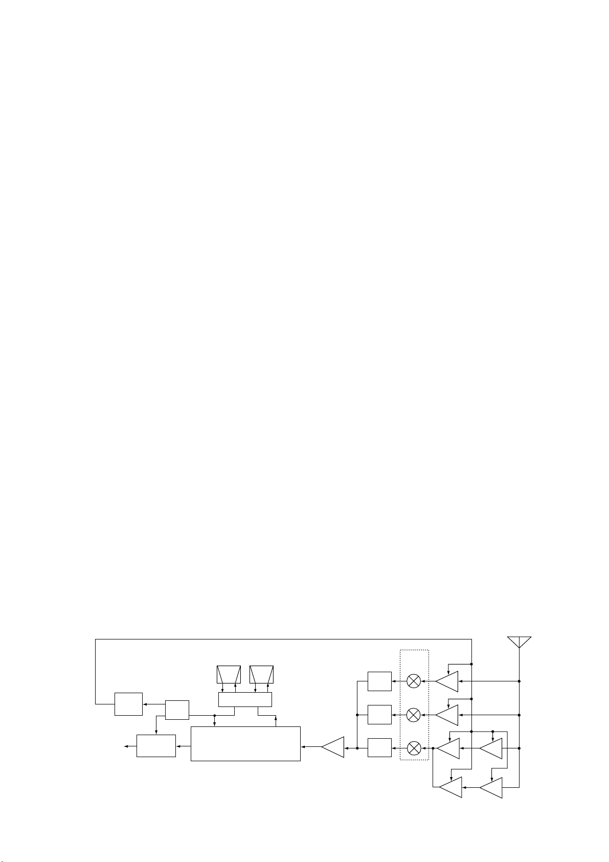
SECTION 4 CIRCUIT DESCRIPTION
LPF
VHF signals (118 174 MHz)
to the 2nd IF circuit
1st mixer (Q32)
Q38
Q39
Q36
Q37 Q41
Q40
1st mixer (Q35)
1st mixer (IC12)
Antenna
UHF signals (430 440 MHz)
LPF
T/R
SW
BPF
RF
AMP
BPF ATT
RX
SW
800M signals (810 1000 MHz)
HPF
RX
SW
BPF
RF
AMP
BPF
ATT
RX
SW
RF
AMP
HPF
T/R
SW
RF
AMP
BPF
BPF
ATT
RX
SW
RX
SW
400M signals (230 550 MHz)
BPF
RF
AMP
RX
SW
RX
SW
RX
SW
RF
AMP
• RF CIRCUITS
Page 10

4 - 2
• ABOVE 230 MHz RF CIRCUIT
(230 MHz–550 MHz, EXCEPT 430 MHZ–440 MHz)
The signals from the attenuator circuit pass through the tunable bandpass filter (D36, L37, L38, C242, C253, C261).
The filtered signals are amplified at the above 230MHz RF
amplifier (Q40) and are then enter another 2-stage tunable
bandpass filter (D25, D30, C205, C212) to suppress
unwanted signals and improve the selectivity. The filtered
signals are applied to the RF amplifier (Q36). The amplified
signals pass through the 400 MHz RX switching circuit
(D17), and then applied to the 400 MHz 1st mixer circuit
(IC12).
• ABOVE 800 MHz RF CIRCUIT (810 MHz–1000 MHz)
The signals from the attenuator circuit pass through the tunable bandpass filter (D37, L39, C243, C254, C260, C269).
The filtered signals are amplified at the above 800 MHz RF
amplifier (Q41) and are then enter another tunable bandpass filter (D26, D31, L27, L31, C188, C197, C206, C213,
C223) to suppress unwanted signals and improve the selectivity. The filtered signals are applied to the RF amplifier
(Q37). The amplified signals pass through the 400 MHz RX
switching circuit (D18), and then applied to the 1st mixer circuit (IC12) same as 400 MHz RF circuit.
The tunable bandpass filters (D11–D13, D15) employ var-
actor diodes to tune the center frequency of the RF passband for wide bandwidth receiving and good image
response rejection.
4-1-5 VHF 1ST MIXER CIRCUIT (MAIN UNIT)
The 1st mixer circuit converts the received signal to a fixed
frequency of the 1st IF signal with a 1st LO frequency.
• VHF 1ST MIXER CIRCUIT
The signals from the VHF RF circuit are mixed with the 1st
LO signal at the 1st mixer circuit (Q32) to produce a 46.05
MHz 1st IF signal. The 1st IF signal passes through the RX
switching circuit (D8), and are then applied to the 1st IF circuit.
• UHF (430 MHz–440 MHz) 1ST MIXER CIRCUIT
The signals from the UHF RF circuit are mixed with the 1st
LO signal at the 1st mixer circuit (Q35) to produce a 46.05
MHz 1st IF signal. The 1st IF signal passes through the RX
switching circuit (D9), and are then applied to the 1st IF circuit.
• ABOVE 230 MHz (EXCEPT 430 MHz–440 MHz) 1ST
MIXER CIRCUIT
The signals from the above 230 MHz and above 800 MHz
RF circuit are mixed with the 1st LO signal at the 1st mixer
circuit (IC12) to produce a 46.05 MHz 1st IF signal. The 1st
IF signal passes through the RX switching circuit (D10), and
are then applied to the 1st IF circuit.
The output 46.05 MHz 1st IF signals from the each RX
switching circuits is applied to the crystal bandpass filter
(FI3), and then passed through the limiter circuit (D6). The
signal is amplified at the IF amplifier (Q18), and then applied
to the 2nd mixer circuit (IC8).
4-1-7 2ND IF AND DEMODULATOR CIRCUITS
(MAIN UNIT)
The 2nd mixer circuit converts the 1st IF signal to a 2nd IF
signal. A double superheterodyne system (which converts
receive signals twice) improves the image rejection ratio and
obtains stable receiver gain.
The FM IF IC (IC8) contains the 2nd local oscillator, 2nd
mixer, limiter amplifier, quadrature detector, and noise
detector circuits, etc.
The 1st IF signal from the IF amplifier is applied to the 2nd
mixer section of IC8 (pin 16), and is mixed with a 45.6 MHz
2nd LO signal generated by the reference oscillator circuit
(Q2, Q3, D1, X1) to produce a 450 kHz 2nd IF signal.
The 2nd IF signal from the 2nd mixer passes through the
ceramic bandpass filter (passes through FI2 during wide
channel spacing selection, or passes through FI1 during
narrow channel spacing selection), where unwanted signals
are suppressed. The ceramic filters (FI1, FI2) are switched
by IC9 and IC10 that is controlled by “WN_SEL” signal from
the MAIN CPU (IC505, pin 99).
The filtered signal is applied to the AM or FM detector circuit
separately.
W/N selector
FI2FI1
AM
DET
AM/FM
selector
2nd IF filter
450 kHz
Q13
Q16
IC9,
IC10,
Q21
Noise
detector
Q2,
Q7
Limiter
amp.
FM
detector
Active
filter
AF signals
("DET" signal)
R5
X2 Discriminator
RSSI
Mixer
45.6 MHz
1st IF from the
IF amplifier (Q18)
"RSSI" signal to the CPU
"SQL" signal to the CPU
8
7
5
BPF
32
3
1612 1411109
IC8
TA31136FN
X1
15.2 MHz
• 2ND IF AND DEMODULATOR CIRCUITS
Page 11
4 - 3
• IN CASE OF FM SIGNAL RECEIVING
The signal is then amplified at the limiter amplifier section
(IC5, pin 5) and applied to the FM detector section (X2, IC5,
pins 10, 11) for demodulation the 2nd IF signal into AF signals.
The FM detector circuit employs a quadrature detection
method (liner phase detection), which uses a ceramic discriminator (X2) for phase delay to obtain a non-adjusting circuit. The detected signal from IC5 (pin 9) passes through the
AM/FM selector circuit (IC5, pins 7, 1), and is then applied
to the AF circuit.
• IN CASE OF AM SIGNAL RECEIVING
The signal is amplified at the amplifier (Q16), and is then
applied to the AM detector circuit (Q13) for demodulation the
2nd IF signal into AF signals.
The detected signal from Q13 passes through the AM/FM
selector circuit (IC5, pins 6, 1), and is then applied to the AF
circuit.
4-1-8 AF AMPLIFIER CIRCUIT (MAIN UNIT)
The AF amplifier circuit amplifies the detected signals to
drive a speaker. The AF circuit includes an AF mute circuit
for the squelch.
The detected AM or FM AF signals are applied to AF mute
circuit (Q14). The output signals pass through the low-pass
filter (Q5), and are then applied to the electric volume circuit
(IC508, pin 1). The signals are applied to the other AF mute
circuit (Q512). The signals are level adjusted at the volume
control IC (IC508), and are amplified at the AF power amplifier (IC510, pin 1) after being passed through the other AF
mute circuit (Q512).
The output signal from IC510 (pin 4) drives the external or
internal speaker.
A part of signals from the AM/FM selector circuit (IC5, pin 1)
pass through low-pass filters.
When the signal passes through the low-pass filter (Q3), the
filtered signal is applied to the MAIN CPU (IC505, pin 39) via
the “DTCS_IN” signal to analyze the DTCS signal.
When the signal passes through the other low-pass filter
(C52, C53, R46, R52), the filtered signal is applied to the
MAIN CPU (IC505, pin 42) via the “WXALT” signal to detect
WX alert signal.
A part of signals from the AF mute circuit (Q14) is applied to
the 6-pins data jack as data signal via the “DATAOUT” signal.
4-1-9 SQUELCH CIRCUIT (MAIN UNIT)
• NOISE SQUELCH
A noise squelch circuit cuts out AF signals when no RF signals are received. By detecting noise components in the AF
signals, the squelch circuit switches the AF mute switch.
Some of the noise components in the AF signals from the
FM IF IC (IC8, pin 9) are passed through the active filter section (IC8, pins 8, 7), and then applied to the noise detector
section. The detected noise signals are applied to the MAIN
CPU (IC505, pin 38) via the “SQL” line.
Even when the squelch is closed, the AF mute switch
(Q512) opens at the moment of emitting beep tone.
• TONE SQUELCH
The tone squelch circuit detects AF signals and opens the
squelch only when receiving a signal containing a matching
subaudible tone (CTCSS). When tone squelch is in use, and
a signal with a mismatched or no subaudible tone is
received, the tone squelch circuit mutes the AF signals even
when noise squelch is open.
A portion of the AF signals from the FM IF IC (IC8, pin 9)
passes through the low-pass filter (Q3) to remove AF (voice)
signals via the AM/FM AF selector (IC5, pins 7, 1), and is
then applied to the CTCSS decoder inside the CPU (IC505,
pin 39) via the “DTCS_IN” line to control the AF mute switch.
4-1-10 AGC CIRCUIT (MAIN UNIT)
The AGC (Automatic Gain Control) circuit reduces IF amplifier gain to keep the audio output at a constant level. The
receiver gain is determined by the voltage on the AGC line
(Q13 collector).
• AGC CIRCUIT
AF signal
D19—D21,
D525
AGC
AM/FM
selector
Q13,
Q16
AM
DET
2nd IF filter
450 kHz
FI2FI1
W/N selector
FM IF IC
IC8
IC9,
IC10,
Q21
Q18
Antenna
1st
mixer
RX
SW
RX
SW
IF
RX
SW
RF
RF
RF
RF
RF
RF
Page 12
4 - 4
The signal from the AM detector circuit (Q13) is detected at
the AGC detector circuit (D19–D21). When receiving strong
signals, the detected voltage increases and the AGC voltage
decreases via the AGC circuit. The AGC voltage is used for
the bias voltage of the receive switching PIN diodes to attenuate the received signals. Therefore, this transceiver keeps
the audio output at a constant level.
4-1-11 S-METER CIRCUIT (MAIN UNIT)
The S-meter circuit indicates the relative received signal
strength while receiving by utilizing the AGC voltage which
changes depending on the received signal strength.
The FM S-meter signal from the FM IF IC (IC8, pin 12) is
applied to the main CPU (IC505, pin 40) as an S-meter signal via the “RSSI” signal line.
The S-meter signal is applied to the sub CPU and is then
displayed on the LCD.
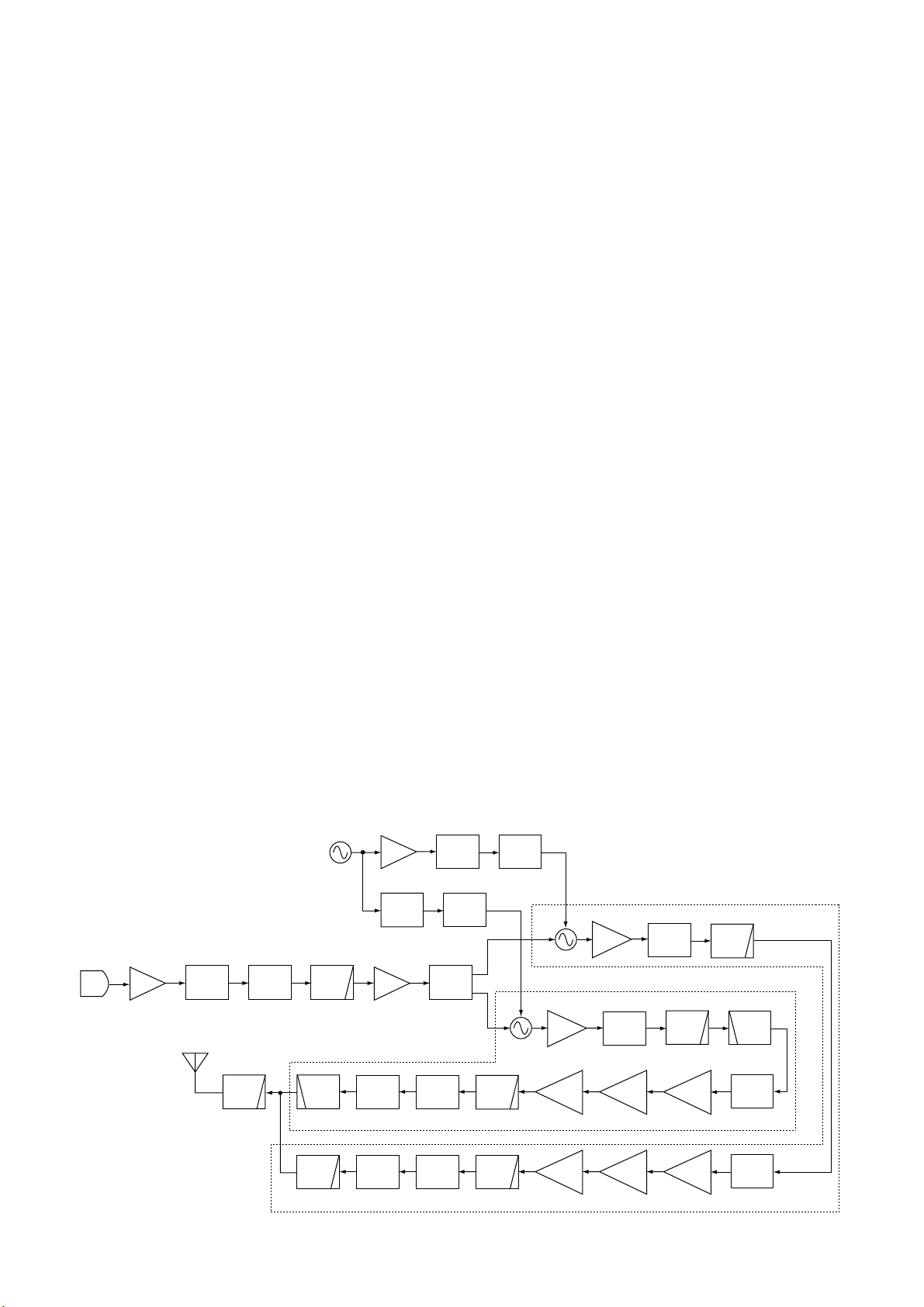
4-2 TRANSMITTER CIRCUITS
4-2-1 MICROPHONE AMPLIFIER CIRCUIT
(MAIN UNIT)
The microphone amplifier circuit amplifies audio signals
from the microphone to a level needed at the modulation circuit. The microphone amplifier circuit is commonly used for
both the VHF and UHF bands.
• AUDIO SIGNALS
The AF signals from the microphone are amplified at the
microphone amplifier (Q505, IC506), and are then applied to
the analog switch (IC509, pin 2). The signals from analog
switch (pin 1) are applied to the IDC amplifier (IC3A, pin 3)
via the “MODIN” line, and then pass through the low-pass filter (IC3D, pins 13, 14) to suppress unwanted components.
IC3A composes limiter amplifier and pre-emphasis circuits.
The signals are amplified at the buffer amplifier (IC3C, pins
9, 8), and are then applied to the D/A converter IC (IC4, pin
13) to adjust modulation level. The signals from the D/A con-
vertor (IC4, pin 23) pass through the reference controller
(D1, X1), and are then applied to the VHF or UHF modulation circuits separately.
• DATA SIGNALS
The data signals from the 6-pins jack (J504, pin 1) pass
through the limiter circuit (D524) to limit the level.
When setting to 9600 bps mode, The signals pass through
the analog switch (IC509, pins 4, 3), and then pass through
the switch again (pins 9, 8). The signals are amplified at the
buffer amplifier (IC3c, pins 9, 8) via the “DATAMOD” line,
and are then applied to the same line as audio signals
(applied to the D/A converter IC’s pin 13).
When setting to 1200 bps mode, The signals pass through
the analog switch (IC509, pins 4, 3), and then pass through
the switch again (pins 10, 11). The signals are then applied
to the same line as “MODIN” (applied to the IDC amplifier;
IC3A, pin 3).
4-2-2 VHF MODULATION CIRCUIT
(MAIN UNIT AND VCO BOARD)
The modulation circuit modulates the VCO oscillating signal
(RF signal) using the microphone audio signals.
The audio or data signals from the reference controller (D1,
X1) are amplified at the buffer amplifier (Q2), and then pass
through the VHF PLL IC (IC1, pins 1,15) and VHF loop filter
(IC6, Q9, Q10, D4). The filtered signals are applied to the VVCO circuit (VCO board).
The signals change the reactance of D1 (VCO board) to
modulate the oscillated signal at the V-VCO circuit (VCO
board; Q3, D1, D2). The modulated signals are amplified at
the buffer amplifiers (VCO board; Q4, Q5), and then passed
through the Tx/Rx switching circuit (VCO board; D5) and
low-pass filter (L6, C32, C33). The filtered signals are
applied to the drive amplifier circuit on the MAIN unit.
Analog
SW
Amp
MIC
Antenna
IC506,
Q505
IC509
IC3A IC3D IC3C IC4
Q102,
Q103
Q2
IC1
IC2
X1
15.2 MHz
Buff
Buff
IDC
PLL IC
Loop
filter
VCO
SW
VCO
SW
LPF
Buffs
Buffs
Pre
drive
Drive
PWR
LPF
SWR
DET
TX/RX
SW
ATT
D/A
PLL IC
Loop
filter
HPFLPF
LPF
VHF TX CIRCUIT
UHF TX CIRCUIT
HPFLPF
Pre
drive
Drive
PWR
LPF
SWR
DET
TX/RX
SW
ATT
LPF
Q31Q34IC14
Q30Q33IC13
• TRANSMITTER CIRCUITS
Page 13
4 - 5
4-2-3 VHF DRIVE AMPLIFIER CIRCUIT
(MAIN UNIT)
The drive amplifier circuit amplifies the VCO oscillating signal to a level needed at the power amplifier.
The RF signals from the low-pass filter (VCO board) pass
through the attenuator (R133, R134, R137), and are then
amplified at the pre-drive (Q30) and drive (Q33, D13) amplifiers to obtain power that IC13 can operate. The amplified
signal is then applied to the RF power amplifier (IC1).
4-2-4 VHF POWER AMPLIFIER CIRCUIT
(MAIN UNIT)
The power amplifier circuit amplifies the driver signal to an
output power level.
IC13 is a power module which has amplification output
capabilities of about 55 W. The RF signal from the drive
amplifier (Q33) is applied to IC13 (pin 1).
The amplified signals from the power amplifier (IC13, pin 4)
pass through the low-pass filter (L22, C193, C189) and
SWR detector (D27, D33), antenna switching circuit (D45)
and other low-pass filter (L45, L46, L49, C279, C282, C285,
C289). The filtered signals are passed through the low-pass
filter (L51, L52, L56, C295, C299) to suppress unwanted signals, and are then applied to the antenna connector (CHASSIS unit J2).
Control voltage for the power amplifier (IC13, pin 2) are controlled by the APC circuit to protect the power module from
a mismatched condition as well as to stabilise the output
power.
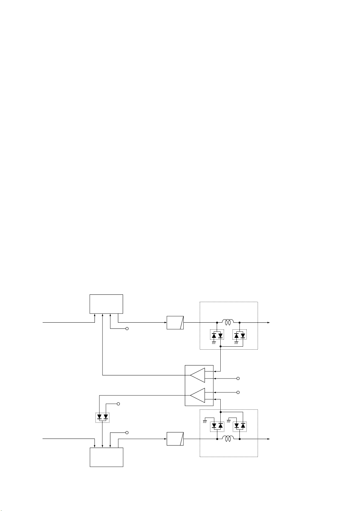
4-2-5 VHF APC CIRCUIT (MAIN UNIT)
The APC circuit protects the power amplifier from a mismatched output load and stabilises transmit output power.
The SWR detector circuit (D27, D33, L29) detects forward
signals and reflection signals at D27 and D33 respectively.
The combined voltage is at a minimum level when the
antenna impedance is matched at 50 Ω and is increased
when it is mismatched.
The detected voltage is applied to the APC amplifier (IC15,
pin 6) and compared with a reference voltage which is supplied from the CPU (IC505) as a “PCON_V” D/A control signal.
When antenna impedance is mismatched, the detected voltage exceeds the reference voltage. The output voltage of
the APC amplifier (IC15, pin 7) controls the bias voltage of
the power module (IC13) to reduce the output power via the
APC controller (IC15,).
4-2-6 UHF MODULATION CIRCUIT
(MAIN UNIT AND VCO BOARD)
The audio or data signals from the reference controller (D1,
X1) pass through the UHF PLL IC (IC2, pins 1,15) and UHF
loop filter (IC6, Q9, Q10, D4), and are then applied to the UVCO circuit (VCO board).
The signals change the reactance of D100 (VCO board) to
modulate the oscillated signal at the U-VCO circuit (VCO
board; Q101, D101, D102). The modulated signals are
amplified at the buffer amplifiers (VCO board; Q102, Q103),
and then passed through the Tx/Rx switching circuit (VCO
board; D103) and low-pass filter (L104, C122, C124). The filtered signals are applied to the drive amplifier circuit on the
MAIN unit.
HV
to the VHF TX/RX switch
to the UHF TX/RX switch
APC controller
(IC15)
VHF SWR detector
IC13
L29
5
6
7
D27 D33
From the VHF
drive amplifier (Q33)
VHF power
amplifier
UHF power
amplifier
HV
IC14
D531
"PL_U" signal from the D/A
convertor (IC11, pin 19)
"PCON_V" signal from the D/A
convertor (IC11, pin 8)
"PCON_V" signal from the D/A
convertor (IC11, pin 9)
L30
3
2
1
D28 D34
From the UHF
drive amplifier (Q34)
LPF
LPF
UHF SWR detector
• APC CIRCUIT
Page 14
4 - 6
4-2-7 UHF DRIVE AMPLIFIER CIRCUIT
(MAIN UNIT)
The RF signals from the low-pass filter (VCO board) pass
through the high-pass filter (L69, C119) and attenuator
(R135, R136, R138), and are then amplified at the pre-drive
(Q31) and drive (Q34, D14) amplifiers to obtain power that
IC14 can operate. The amplified signal is then applied to the
RF power amplifier (IC4).
4-2-8 UHF POWER AMPLIFIER CIRCUIT
(MAIN UNIT)
IC14 is a power module which has amplification output
capabilities of about 50 W. The RF signal from the drive
amplifier (Q34) is applied to IC14 (pin 1).
The amplified signals from the power amplifier (IC14, pin 4)
pass through the low-pass filter (L23, C190) and SWR
detector (D28, D34), antenna switching circuit (D40) and
high-pass filter (L47, L50, C284, C288, C292). The filtered
signals are passed through the low-pass filter (L51, L52,
L56, C295, C299) to suppress unwanted signals, and are
then applied to the antenna connector (CHASSIS unit J2).
Control voltage for the power amplifier (IC14, pin 2) are controlled by the APC circuit to protect the power module from
a mismatched condition as well as to stabilise the output
power.
4-2-9 UHF APC CIRCUIT (MAIN UNIT)
The SWR detector circuit (D28, D34, L30) detects forward
signals and reflection signals at D28 and D34 respectively.
The combined voltage is at a minimum level when the
antenna impedance is matched at 50 Ω and is increased
when it is mismatched.
The detected voltage is applied to the APC amplifier (IC15,
pin 3) and compared with a reference voltage which is supplied from the CPU (IC505) as a “PCON_U” D/A control signal.
When antenna impedance is mismatched, the detected voltage exceeds the reference voltage. The output voltage of
the APC amplifier (IC15, pin 1) controls the bias voltage of
the power module (IC14) to reduce the output power via the
APC controller (IC15, D531).
4-3 PLL CIRCUITS
4-3-1 GENERAL (MAIN UNIT)
A PLL circuit provides stable oscillation of the transmit frequency and the receive local frequency. The PLL circuit
compares the phase of the divided VCO frequency to the
reference frequency. The PLL output frequency is controlled
by a crystal oscillator and the divided ratio of the programmable divider. IC1 and IC2 are dual PLL ICs that control both
VCO circuits for VHF and UHF.
4-3-2 VHF LOOP (VCO BOARD AND MAIN UNIT)
The generated signal at the V-VCO (Q3, D1, D2) enters the
PLL IC (MAIN unit; IC1, pin 8) via buffer-amplifiers (Q6, Q8)
and VCO switching circuit (D50) and is divided at the programmable divider section and is then applied to the phase
detector section.
The phase detector compares the input signal with a reference frequency, and then outputs the out-of-phase signal
(pulse-type signal) from pin 15 (MAIN unit).
The pulse-type signal is converted into DC voltage (lock
voltage) at the loop filter (MAIN unit; IC5, Q9, Q10, D4), and
then applied to the V-VCO to stabilise the oscillated frequency.
• VHF PLL CIRCUIT
VHF VCO
Q3, D1, D2
Loop
filter
16
Phase
15
detector
VCO
switch
Q4
Buffer
Programmable
counter
Q5
Buffer
VCO
switch
Buffer
D51
IC1 MB15A02PFV1
Prescaler
Q50
D5
D6
8
to the transmitter circuit
to the 1st mixer circuit
X2
15.2 MHz
Q2
Buffer
1
Buffer
Q7
Programmable
divider
45.6 MHz 2nd LO signal
to the FM IF IC (IC8, pin 3)
Shift register
9
10
11
PLLCK
PLLDATA
PLLSTB1
Page 15

4 - 7
4-3-3 UHF LOOP (VCO BOARD AND MAIN UNIT)
The generated signal at the U-VCO (Q101, D100, D101)
enters the PLL IC (MAIN unit; IC2, pin 8) via buffer-amplifiers (Q102, Q50) and VCO switching circuit (D51) and is
divided at the programmable divider section and is then
applied to the phase detector section.
The phase detector compares the input signal with a reference frequency, and then outputs the out-of-phase signal
(pulse-type signal) from pin 15 (MAIN unit).
The pulse-type signal is converted into DC voltage (lock
voltage) at the loop filter (MAIN unit; IC7, Q11, Q12, D5),
and then applied to the U-VCO to stabilise the oscillated frequency.
4-3-4 1ST LO CIRCUIT
(VCO BOARD AND MAIN UNIT)
The 1st VCO circuit contains a separate V-VCO (Q3, D1,
D2) and U-VCO (Q101, D100, D101).
• WHILE RECEIVING VHF BAND
The oscillated signal at the V-VCO circuit is amplified at the
buffer amplifier (Q4), and is then applied to the VCO switching circuit (D6). The signal passes through the attenuator
(C34, R24–R26) and low-pass filter (L7, L8, C36–C38), and
is then applied to the LO switching circuit.
(1) RECEIVING 118MHz–174 MHz
The signal is applied to the LO switching circuit (MAIN unit;
D528) as “V_RXLO” signal, and is applied to the 1st mixer
circuit (MAIN unit; Q32), then mixed with the 1st IF signal.
(2) RECEIVING 230 MHz–550 MHz
The signal is applied to the LO switching circuit (MAIN unit;
D15, D529, D530) as “V_RXLO” signal, and is applied to the
1st mixer circuit (MAIN unit; Q35), then mixed with the 1st IF
signal.
A portion of the RF signal from the buffer amplifier (Q4) is
amplified at the buffer amplifier (Q50), and is then fed back
to the PLL IC (MAIN unit; IC1, pin 8) as the comparison signal.
• WHILE RECEIVING UHF BAND OR 800 MHz BAND
The oscillated signal at the U-VCO circuit is amplified at the
buffer amplifiers (Q102, Q103), and is then applied to the
VCO switching circuit (for UHF band; D104, for 800 MHz;
D105).
While receiving UHF band, the signal passes through the
attenuator (C125, R117, R119, R120) and low-pass filter
(Q105, L7, L8, C36–C38), and is then applied to the VCO
switching circuit (D106).
While receiving 800 MHz band, the signal is doubled at the
doubler amplifier (Q104), and passes through the bandpass
filter (L108–L110, C127, C129, C132, C133, C135) and
attenuator (R127, R128). The signal is applied to the VCO
switching circuit (D107).
(1) RECEIVING UHF BAND
The signal is applied to the LO switching circuit (MAIN unit;
D9) as “U_RXLO” signal, and is applied to the 1st mixer circuit (MAIN unit; Q35), then mixed with the 1st IF signal.
(2) RECEIVING 800 MHz BAND
The signal is applied to the LO switching circuit (MAIN unit;
D10) as “U_RXLO” signal, and is applied to the 1st mixer circuit (MAIN unit; IC12, pin 6), then mixed with the 1st IF signal.
A portion of the RF signal from the buffer amplifier (Q102) is
amplified at the buffer amplifier (Q50) via the VCO switching
circuit (D51), and is then fed back to the PLL IC (MAIN unit;
IC1, pin 8) as the comparison signal.
Shift register
Prescaler
Phase
detector
Loop
filter
Programmable
counter
Programmable
divider
X2
15.3 MHz
1
Buffer
Buffer
Buffer
9
10
11
PLLCK
PLLDATA
PLLSTB2
to the 1st mixer circuit
to the 1st mixer circuit
D105
Q104
to the transmitter circuit
D103
D104
15
8
IC2 MB15A02PFV1
Q101, D100, D101
UHF VCO
16
Q102
D51
VCO
switch
VCO
switch
Q103
Q50
2
• UHF PLL CIRCUIT
Page 16

4 - 8
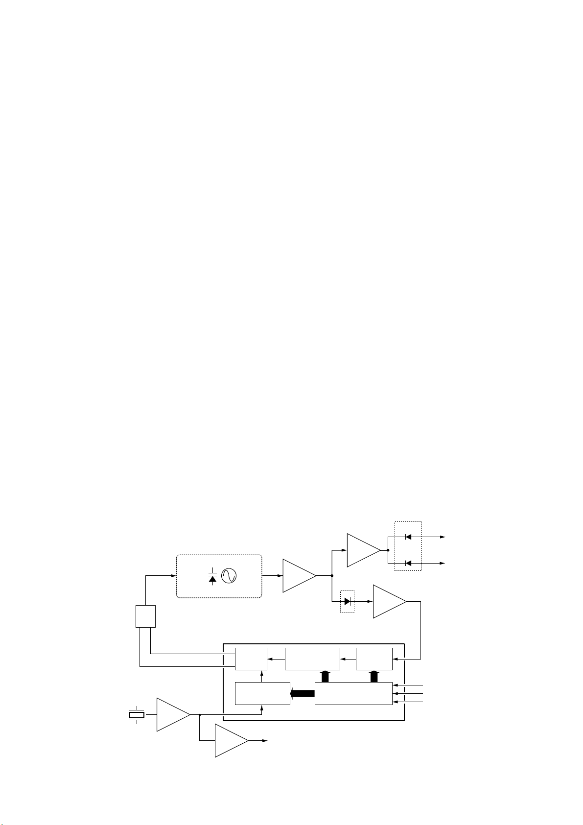
4-4 OTHER CIRCUITS
4-4-1 SUB-CPU RESET CIRCUIT (CONTROL UNIT)
IC2 is the reset voltage detecting circuit. The output voltage
from the +5 regulator circuit (IC5) is applied to the VDD terminal (IC2, pin 2). IC2 outputs “H” (high) signal to the subCPU (IC6, pin 15) when the VDD terminal’s voltage is higher than detecting voltage.
IC6 employs the 8-bit CPU.
4-4-2 LCD DISPLAY CIRCUIT (CONTROL UNIT)
The transceiver’s LCD display employs 1/4 duty custom
LCD which displays frequency, S-meter, TX power level, etc.
The LCD display is controlled by the sub-CPU (IC6, pins
41–78) directly.
4-4-3 LCD AND KEY BACK LIGHT CIRCUIT
(CONTROL UNIT)
The sub-CPU (IC6) outputs +8 regulator circuit (Q1, Q3, D5)
control signal from pin 2. The voltage from +8 regulator circuit is applied to the key back light circuit (DS13–DS18,
DS20, DS23) and LCD back light circuit (DS22).
The back light color is also controlled by the sub-CPU via
the color control circuit (Q6, Q7). The back light has 3 colors
(Umber, Green and Yellow).
Description
The voltage from the external power supply via
the W501 (OPC-465).
The same voltage as the HV line which is controlled by the VCC regulator circuit (Q501). The
circuit is controlled by the power switch controller
(Q502).
Common 8 V converted from the VCC line by the
+8 regulator circuit (IC504).
Transmit 8 V for VHF band which is the same
voltage as the 8V line controlled by the VT8 regulator circuit (Q19, Q22) using the “VTXC” line.
Transmit 8 V for UHF band which is the same
voltage as the 8V line controlled by the UT8 regulator circuit (Q20, Q23) using the “UTXC” line.
Common 5 V converted from the HV line by the
+5 regulator circuit (IC503).
Common 5 V converted from the 5V line by the
+5 regulator circuit(Q503, D504). The circuit is
controlled by the power switch controller (Q502).
Common 8 V converted from the 8 V line by the
+8 regulator circuit (Q4).
Common 8 V line which is selected by the
SEL_SW circuit (Q6, Q8). The voltage is applied
to the VHF VCO (VCO board; Q3, D1, D2) and
buffer amplifiers (VCO board; Q4, Q5).
Common 8 V line which is selected by the
SEL_SW circuit (Q6, Q8). The voltage is applied
to the UHF VCO (VCO board; Q101, D100,
D101) and buffer amplifiers (VCO board; Q102,
Q103).
Receive 5 V line converted from the 5VS line by
the R5 regulator circuit (Q24). The circuit is controlled by the “R5CTRL” signal from the CPU
(IC505, pin 78).
Receive 5 V line for AM circuit converted from the
5VS line by the AM5 regulator circuit (Q25). The
circuit is controlled by the “AM” signal from the
CPU (IC505, pin 69).
Receive 5 V line for VHF circuit converted from
the 5VS line by the VHF_R5 regulator circuit
(Q26). The circuit is controlled by the “RXVHF”
signal from the CPU (IC505, pin 73).
Receive 5 V line for UHF circuit converted from
the 5VS line by the UHF_R5 regulator circuit
(Q27). The circuit is controlled by the “RXUHF”
signal from the CPU (IC505, pin 74).
Receive 5 V line for 400 MHz circuit converted
from the 5VS line by the 400_R5 regulator circuit
(Q28). The circuit is controlled by the “RX400”
signal from the CPU (IC505, pin 67).
Receive 5 V line for 800 MHz circuit converted
from the 5VS line by the 800_R5 regulator circuit
(Q29). The circuit is controlled by the “RX800”
signal from the CPU (IC505, pin 66).
Line
HV
VCC
8V
VT8
UT8
5V
5VS
VCO8
V_VCO8
U_VCO8
R5
AM5
VHF_R5
UHF_R5
400_R5
800_R5
4-5-2 MAIN UNIT VOLTAGE LINES
Description
Common 8 V converted from the HV line by the
+8 regulator circuit (Q1, Q3, D5). The output voltage is applied to the LCD back light (DS22) and
key back light (DS13–DS18, DS20, DS21, DS23)
circuits.
Common 5 V converted from the HV line by the
+5 regulator circuit (IC5, D4). The output voltage
is applied to the reset circuit (IC2) and buffer
amplifier (Q2).
Line
8V
CPU5V
4-5 POWER SUPPLY CIRCUITS
4-5-1 CONTROL UNIT VOLTAGE LINES
Page 17

4 - 9
50
51
52
53
55
56
57
58
62
63
65
66
67
72
73
74
77
78
Input port for the cloning signal.
Outputs the data signal to the D/A
CONVERTER (IC11, pin 17).
Outputs the clock signal to the D/A
CONVERTER (IC11, pin 16).
Outputs the strobe signal to the D/A
CONVERTER (IC1, pin 15).
Outputs the AF mute control signal.
High : While AF signal is muting.
Outputs the strobe signal to the UHF
PLL IC (IC2, pin 11)
Outputs the strobe signal to the VHF
PLL IC (IC1, pin 11)
Outputs the detector circuit mute signal.
High : While the detector circuit is
muting.
Outputs microphone sensitivity control
signal.
High : The sensitivity is high.
Outputs the UHF VCO control signal.
High : The VCO circuit oscillates
320–999.99 MHz signal.
Outputs packet baud rate select signal.
Low : 9600 bps is selected.
Outputs the 800_R5 regulator (Q29)
control signal.
High : While receiving 630–999
MHz.
Outputs the 400_R5 regulator (Q28)
control signal.
High : While receiving 230–630
MHz.
Outputs the UHF_R5 regulator (Q27)
control signal.
High : While receiving 430–450
MHz.
Outputs the VHF_R5 regulator (Q26)
control signal.
High : While receiving 118–174
MHz.
Outputs modulation mute control signal to the VCO circuits.
High : While modulation is muting.
Outputs the microphone muting control signal.
Low : While the microphone is
muted.
Outputs the R5 regulator (Q24) control
signal.
Low : While receiving.
CLONE_IN
DA_DATA
DA_CK
DA_STB
AF_MUTE
PLLSTB2
PLLSTB1
DET_MUTE
MIC_SENS
U_VCO
1200_9600SEL
RX800
RX400
RXUHF
RXVHF
MMUTE
MIC_MUTE
R5CTRL
(MAIN unit; IC505)–Continued
Pin Port
Description
number name
16
17
20
21
22
24
25
26
27
28
31
38
40
41
42
44
45
47
48
49
Outputs the transmit mute signal.
High : While transmit is muting.
Input port for the microphone PTT signal.
High : While PTT switch is pushed.
Outputs the UHF transmitting power
supply circuit control signal.
High : While transmitting (400–479
MHz)
Outputs the VHF transmitting power
supply circuit control signal.
High : While transmitting (136–174
MHz)
Outputs the DTCS filter select signal.
High : While the DTCS signal is
transmitting.
I/O port for the serial data to the EEPROM (IC501, pin 5).
Outputs the clock signal to the EEPROM (IC501, pin 6).
Input port for the packet [PTT] switch.
Low : While the packet [PTT] switch
is ON
Outputs the packet modulation muting
signal.
Low : While muting.
Input port for the HM-98’s data signal.
Input port for the connecting microphone detect signal.
Low : While the HM-98 is connect-
ed.
Input port for the squelch level signal.
Input port for the RSSI signal from the
FM IF IC (IC8, pin 12) to detect receiving signal strength.
Input port for the transceiver’s internal
temperature signal.
Input port for the WX alert (1050 Hz)
signal.
Outputs DTMF, E-TONE and BEEP
signals.
Outputs CTCSS and DTCS signals.
Outputs the packet squelch control
signal.
High : While the squlech is opened.
Outputs the cooling fan control signal.
High : While the cooling fan is
worked.
Outputs the cloning signal.
4-6 PORT ALLOCATIONS
4-6-1 MAIN CPU PORT ALLOCATIONS
(MAIN UNIT; IC505)
TX_MUTE
MIC_PTT
UTXC
VTXC
DTCS_SEL
ES_DATA
ES_CK
P-PTT
P_MOD_MUTE
98_DATA
MIC_SEL
SQL
RSSI
TEMP
WXALT
DTMF
DTCS
P_SQL
FAN_CTRL
CLONE_OUT
Pin Port
Description
number name
Page 18

4 - 10
79
81
83
84
86–89
90
91
93–96
99
Outputs the VCO circuit select signal.
High : The VCO circuit oscillates
203.95–263.945 MHz signal.
Outputs the VHF VCO select signal.
High : The VHF VCO’s power supply
(Q6, Q8) is ON.
Outputs the PLL loop control signal.
Input port for the PLL unlock signal.
High : While the loop is unlocked.
Input ports for the initial matrix signals.
Outputs the PLL data signal to the PLL
ICs (IC1, IC2).
Outputs the PLL clock signal to the
PLL ICs (IC1, IC2).
Output the initial matrix strobe signals
Outputs the wide/narrow FM select
signal.
Low : While selected narrow FM.
VCO_SHIFT
V_VCO
PLLSW
UNLK
MATRIX_
IN1–IN4
PLLDATA
PLLCK
OUT1–OUT4
WN_SEL
Pin Port
Description
number name
(MAIN unit; IC505)–Continued
2–4
5
6
7
8
9
12
13
18
Output the VHF bandpass filter tracking signals.
Outputs the UHF bandpass filter tracking signal.
Outputs the receiving attenuator control signal.
Outputs the bandpass filter shift control signal.
Low : While receiving 450–629.995
MHz.
Outputs the VHF output power control
signal.
Outputs the UHF output power control
signal.
Outputs the 800 MHz bandpass filter
tracking signal.
Outputs the reference frequency control signal.
Outputs the excess current detecting
signal.
TUNE_V1–V3
TUNE_U
ATT
BSHIFT
PCON_V
PCON_U
TUNE_8
REF_CON
REF_V
Pin Port
Description
number name
4-6-2 D/A CONVERTER IC PORT ALLOCATIONS
(MAIN UNIT; IC11)
1
3
4
5
6
7
8
24
25
30
31
39–42
43–78
83
86
88
89
Input port for the [BAND] key.
Low : The [BAND] key is pushed.
Outputs the umber LED control signal.
High : The LED lights ON.
Input port for the [S.MW] key.
Low : The [S.MW] key is pushed.
Input port for the [TONE] key.
Low : The [TONE] key is pushed.
Input port for the [LOW] key.
Low : The [LOW] key is pushed.
Input port for the [MONI] key.
Low : The [MONI] key is pushed.
Input port for the [SET] key.
Low : The [SET] key is pushed.
Input port for the [M/CALL] key
Low : The [M/CALL] key is pushed.
Input port for the [V/MHz] key.
Low : The [V/MHz] key is pushed.
Input port for the main dial’s A phase
signal.
Input port for the main dial’s B phase
signal.
Output the common signals to the LCD
(DS1).
Output the segment signals to the LCD
(DS1).
Outputs the green LED control signal.
High : The LED lights ON.
Input port for the [PWR] key.
Low : The [PWR] key is pushed.
Input port for the [VOL] controller.
Input port for the [SQL] controller.
4-6-3 FRONT CPU PORT ALLOCATIONS
(CONTROL UNIT; IC6)
BAND
A_LED
SMW
TONE
LOW
MONI
SET
M/CALL
VMHz
DIAL_A
DIAL_B
COM4–COM1
SEG1–SEG36
G_LED
PWR
VOL
SQL
Pin Port
Description
number name
Page 19

5 - 1
5-1 PREPARATION
Need to enter the adjustment mode, and the JIG calble as shown the page 5-2 is required when adjusting the IC-208H.
■ REQUIRED TEST EQUIPMENT
DC power supply
RF power meter
(terminated type)
Frequency counter
Standard signal
generator (SSG)
FM deviation meter
Oscilloscope
Audio generator
Attenuator
EQUIPMENT GREDE AND RANGE EQUIPMENT GREDE AND RENGE
SECTION 5 ADJUSTMENT PROCEDURES
Output voltage : 13.8 V DC
Current capacity : 12 A or more
Measuring range : 0.1–100 W
Frequency range : 1.8–600 MHz
Impedance : 50 Ω
SWR : Less than 1.2 : 1
Frequency range : 0.1–600 MHz
Frequency accuracy : ±1 ppm or better
Sensitivity : 100 mV or better
Frequency range : 0.1–1200 MHz
Output level : 0.1 µV–32 mV
(–127 to –17 dBm)
Frequency range : 0–600 MHz
Measuring range : 0 to ±5 kHz
Frequency range : DC–600 MHz
Measuring range : 0.01–10 V
Frequency range : 300–3000 Hz
Measuring range : 1–500 mV
Power attenuation : 50 or 60 dB
Capacity : 150 W or more
■ ENTERING THE ADJUSTMENT MODE
q Turn the transceiver’s power OFF.
w Connect the JIG cable to the [MIC] jack.
e Push and hold the [SET] and [BAND] keys, and then turn power ON.
NOTE: Exiting from the adjustment mode when the transciever’s power is OFF.
■ OPERATING ON THE ADJUSTMENT MODE
• Change the adjustment value : [DIAL]
• Verifying the adjustment value : [M/CALL] key
• Forward the adjustment item : [SET/LOCK] key
• Go back the adjustment item : [S.MW/MW] key
• Store the adjustment value in the memory : [BAND] key
CAUTION: Need to push the [BAND] key when storing the adjustment value in the memory. Otherwise, the transceiver is not
adjusted properly.
NOTE: *Need to adjust about manually adjustment items.
ADJUSTMENT ITEMS
Reference frequency’s temp. correction
Reference voltage
Protect time
Protect temperature
Cooling fan temperature
DTCS wave form
DTCS/CTCSS amplitude
*S-Meter
*Squelch level (Wide)
*Squelch level (Narrow)
DISPLAY
[Fr1]–[Fr8]
[rE–], [rE+]
[PT]
[PCV], [PCU]
[FT]
[DTA], [DTB]
[DT], [CT]
[SL]
[SqW]
[SqN]
ATTENTION!: DO NOT adjust following adjusment items (Because they are adjusted automatically when other
adjustment items are adjusted). Otherwise, the transceiver do not work properly. Refer to the next
page in detail.
Page 20

5 - 2
‘‘
CONNECTIONS
pin 6 (MIC)
pin 4 (PTT)
pin 7 (GND)
pin 2 (MICU/D)
pin 5 (MICE)
to the antenna connector
STANDARD SIGNAL GENERATOR
0.1 300 MHz
127 to 17 dBm (0.1 V to 32 mV)
RF POWER METER
50 , 1 80 W
FM DEVIATION
METER
ATTENUATOR
50 dB or 60 dB
POWER SUPPLY
13.8 V, 20 A or more
CAUTION!
DO NOT transmit
while an SSG is
connected to the
antenna connector.
JIG CABLE INFORMATION
to the microphone connector
2.2 k
AUDIO GENERATOR
300 Hz to 3 kHz
ADJUSTMENT ITEM EXPLANATION
[Fr]
*[Fr1]*[Fr2]*[Fr3]*[Fr4]*[Fr5]*[Fr6]*[Fr7]*[Fr8]
[rE]
*[rE+][HP ]
[PM]
*[PCV]*[PCU]*[FT]*[DTA]*[DTB]*[DT]*[SL] *[CT]*[DT]*[CT]
[PP]
*[PT]
[HP+] [MP+] [LP+] [HP+] [MP+] [LP+]
[POH]
Starting item
[POM] [POL] [POH] [POM] [POL] [PL] [PV] [DE] [DT] [Tr] [SL]
[SqW][SqN]
*[SqW]*[SqN]
*[rE ]
[LP ][MP ][HP ][LP ][MP ]
*Not adjust items
DISPLAY
[Fr]
[rF]
[POH], [POM], [POL]
[PL]
[PV]
[DE]
[DT]
[Tr]
[SL]
[SqW]
[SqN]
*[Fr1], *[Fr2], *[Fr3], *[Fr4],
*[Fr5], *[Fr6], *[Fr7], *[Fr8]
ADJUSTMENT ITEMS
Reference frequency
Reference voltage
VHF/UHF output power
Transmit minimum voltage
Protect voltage
Frequency deviation
DTCS wave form
Tracking
S-Meter
Squelch level (Wide)
Squelch level (Narrow)
Reference frequency’s
temperature correction
DISPLAY
*[rE–], *[rE+]
[HP–], [HP+], [MP–],
[MP+], [LP–],[MP+]
[PM]
[PP]
*[PT]
*[PCV], *[PCU]
*[FT]
*[DTA], *[DTB]
*[DT], *[CT]
*[SL]
*[SqW]
*[SqN]
ADJUSTMENT ITEMS
Reference voltage
Temperature correction
Protect scale
Protect power
Protect time
Protect temperature
Cooling fan temperature
DTCS wave form
DTCS/CTCSS amplitude
S-Meter
Squelch level (Wide)
Squelch level (Narrow)
Page 21

5 - 3
5-2 SOFTWARE ADJUSTMENTS (TRANSMITTING)
REFERENCE
FREQUENCY
[Fr]
REFERENCE
VOLTAGE
[rE]
VHF
OUTPUT
POWER
(High)
[POH]
(Middle)
[POM]
(Low)
[POL]
UHF
OUTPUT
POWER
(High)
[POH]
(Middle)
[POM]
(Low)
[POL]
TRANSMIT
MINIMUM
VOLTAGE
[PL]
PROTECT
VOLTAGE
[PV]
1
1
1
2
3
1
2
3
1
2
3
1
2
• Operating frequency : 445.0 MHz
• Loosely couple a frequency counter to the antenna
connector on the rear panel.
• Transmitting
• Operating frequency : 445.0 MHz
• Receiving
• Operating frequency : 146.0 MHz
• Connect an RF power meter to the antenna connector.
• Transmitting
• Transmitting
• Transmitting
• Operating frequency : 445.0 MHz
• Connect an RF power meter to the antenna connector.
• Transmitting
• Transmitting
• Transmitting
• Operating frequency : 440.0 MHz
• Connect an RF power meter to the antenna connector.
• Transmitting
• Operating frequency : 445.0 MHz
• Transmitting
• Operating frequency : 450.0 MHz
• Transmitting
• Operating frequency : 146.0 MHz
• [High]/[Middle]/[Low] swtich : High
• Connect an RF power meter to the antenna connector.
• Transmitting
• Operating frequency : 445.0 MHz
• Transmitting
• Turn the [DIAL] to set to 445.0000 MHz.
• Push the [BAND] key.
• Push the [BAND] key.
• Turn the [DIAL] to set the VHF high power to 55 W.
• Push the [BAND] key.
•
Turn the [DIAL] to set the VHF middle power to 15 W.
• Push the [BAND] key.
• Turn the [DIAL] to set the VHF low power to 5 W.
• Push the [BAND] key.
• Turn the [DIAL] to set the UHF high power to 50 W.
• Push the [BAND] key.
•
Turn the [DIAL] to set the UHF middle power to 15 W.
• Push the [BAND] key.
• Turn the [DIAL] to set the UHF low power to 5 W.
• Push the [BAND] key.
• Turn the [DIAL] to set to 1 W.
• Push the [BAND] key.
• Turn the [DIAL] to set to 1 W.
• Push the [BAND] key.
• Turn the [DIAL] to set to 1 W.
• Push the [BAND] key.
• Push the [BAND] key.
• Push the [BAND] key.
ADJUSTMENT ADJUSTMENT CONDITION OPERATION
Page 22

5 - 4
SOFTWARE ADJUSTMENTS (TRANSMITTING AND RECEIVING)–Continued
FREQUENCY
DEVIATION
(VHF band)
[DE]
(UHF band)
[DE]
DTCS WAVE
FORM
(VHF band)
[DE]
(UHF band)
[DE]
TRACKING
(Low band)
[Tr]
(Middle1
band)
[Tr]
1
2
3
4
1
2
1
2
3
4
5
6
7
8
• Operating frequency : 144.0 MHz
• Connect an audio generator to the [MIC] jack and set
as : +20 dB
• Connect an FM deviation meter to the antenna connector and set as :
HPF : 50 Hz
LPF : 20 kHz
De-emphasis : OFF
Detector : (P–P)/2
• Transmitting
• Operating frequency : 148.0 MHz
• Transmitting
• Operating frequency : 440.0 MHz
• Transmitting
• Operating frequency : 450.0 MHz
• Transmitting
• Operating frequency : 146.0 MHz
• No audio signal is applied to the [MIC] jack.
• DTCS code : 007
• Set an FM deviation meter as:
HPF : OFF
LPF : 20 kHz
De-emphasis : OFF
Detector : (P–P)/2
• Transmitting
• Operating frequency : 445.0 MHz
• Transmitting
• Operating frequency : 118.1 MHz
• Connect an SSG to the antenna connector and set as
Level : 1 µV* (–107 dBm)
Modulation : 1 kHz
Deviation : ± 3.5 kHz
• Receiving
• Operating frequency : 146.1 MHz
• Receiving
• Operating frequency : 160.1 MHz
• Receiving
• Operating frequency : 173.9 MHz
• Receiving
• Operating frequency : 230.1 MHz
• Connect an SSG to the antenna connector and set as
Level : 1 µV* (–107 dBm)
Modulation : 1 kHz
Deviation : ± 3.5 kHz
• Receiving
• Operating frequency : 260.1 MHz
• Receiving
• Operating frequency : 380.1 MHz
• Receiving
• Operating frequency : 399.9 MHz
• Receiving
• Turn the [DIAL] to set to ±4.6 kHz.
• Push the [BAND] key.
• Turn the [DIAL] to set to ±4.6 kHz.
• Push the [BAND] key.
• Turn the [DIAL] to set to ±4.6 kHz.
• Push the [BAND] key.
• Turn the [DIAL] to set to ±4.6 kHz.
• Push the [BAND] key.
• Turn the [DIAL] to set to flat wave form as shown
below.
• Push the [BAND] key.
• Turn the [DIAL] to set to flat wave form as same as
VHF band.
• Push the [BAND] key.
• Push the [BAND] key.
• Push the [BAND] key.
• Push the [BAND] key.
• Push the [BAND] key.
• Push the [BAND] key.
• Push the [BAND] key.
• Push the [BAND] key.
• Push the [BAND] key.
ADJUSTMENT ADJUSTMENT CONDITION OPERATION
*This output level of a standard signal generator (SSG) is indicated as SSG’s open circuit.
Set to flat wave
form
Page 23

5 - 5
SOFTWARE ADJUSTMENT (RECEIVING)–Continued
TRACKING
(Middle2
band)
[Tr]
(High band)
[Tr]
S-METER
[SL]
9
10
11
12
13
14
15
1
2
3
4
• Operating frequency : 400.1 MHz
• Connect an SSG to the antenna connector and set as
Level : 1 µV* (–107 dBm)
Modulation : 1 kHz
Deviation : ± 3.5 kHz
• Receiving
• Operating frequency : 429.9 MHz
• Receiving
• Operating frequency : 480.1 MHz
• Receiving
• Operating frequency : 549.9 MHz
• Receiving
• Operating frequency : 810.1 MHz
• Connect an SSG to the antenna connector and set as
Level : 1 µV* (–107 dBm)
Modulation : 1 kHz
Deviation : ± 3.5 kHz
• Receiving
• Operating frequency : 905.1 MHz
• Receiving
• Operating frequency : 999.9 MHz
• Receiving
• Operating frequency : 146.1 MHz
• Connect an SSG to the antenna connector and set as
Level : 1 µV* (–107 dBm)
Modulation : 1 kHz
Deviation : ± 3.5 kHz
• Receiving
• Operating frequency : 445.1 MHz
• Receiving
• Operating frequency : 435.9 MHz
• Receiving
• Operating frequency : 810.1 MHz
• Set an SSG as
Level : 5.6 µV* (–92 dBm)
Modulation : 1 kHz
Deviation : ± 3.5 kHz
• Receiving
• Push the [BAND] key.
• Push the [BAND] key.
• Push the [BAND] key.
• Push the [BAND] key.
• Push the [BAND] key.
• Push the [BAND] key.
• Push the [BAND] key.
• Push the [BAND] key.
• Push the [BAND] key.
• Push the [BAND] key.
• Push the [BAND] key.
ADJUSTMENT ADJUSTMENT CONDITION OPERATION
*This output level of a standard signal generator (SSG) is indicated as SSG’s open circuit.
Page 24

5 - 6
SOFTWARE ADJUSTMENT (RECEIVING)–Continued
SQUELCH
LEVEL
(Wide)
[SqW]
(Narrow)
[SqN]
TEMP.
CORRECTION
<High power>
(VHF –10˚C)
[HP–]
(VHF +60˚C)
[HP–]
<Mid. power>
(VHF –10˚C)
[MP–]
(VHF +60˚C)
[MP–]
<Low power>
(VHF –10˚C)
[LP–]
(VHF +60˚C)
[LP–]
1
2
3
4
5
6
7
8
1
2
3
4
5
6
• Operating frequency : 146.1 MHz
• Connect an SSG to the antenna connector and set as
Level : 0.079 µV* (–129 dBm)
Modulation : 1 kHz
Deviation : ± 3.5 kHz
• Receiving
• Operating frequency : 445.1 MHz
• Receiving
• Operating frequency : 435.1 MHz
• Set an SSG as:
Level : 0.1 µV* (–127 dBm)
• Receiving
• Operating frequency : 810.1 MHz
• Set an SSG as:
Level : 0.25 µV* (–119 dBm)
• Receiving
• Operating frequency : 146.1 MHz
• Connect an SSG to the antenna connector and set as
Level : 0.071 µV* (–130 dBm)
Modulation : 1 kHz
Deviation : ± 3.5 kHz
• Receiving
• Operating frequency : 445.1 MHz
• Receiving
• Operating frequency : 435.1 MHz
• Set an SSG as:
Level : 0.1 µV* (–127 dBm)
• Receiving
• Operating frequency : 810.1 MHz
• Set an SSG as:
Level : 0.25 µV* (–119 dBm)
• Receiving
• Operating frequency : 146.0 MHz
• Receiving
• Operating frequency : 146.0 MHz
• Receiving
• Operating frequency : 146.0 MHz
• Receiving
• Operating frequency : 146.0 MHz
• Receiving
• Operating frequency : 146.0 MHz
• Receiving
• Operating frequency : 146.0 MHz
• Receiving
• Push the [BAND] key.
• Push the [BAND] key.
• Push the [BAND] key.
• Push the [BAND] key.
• Push the [BAND] key.
• Push the [BAND] key.
• Push the [BAND] key.
• Push the [BAND] key.
•Turn the [DIAL] to set to “F9” on the display.
• Push the [BAND] key.
•Turn the [DIAL] to set to “F9” on the display.
• Push the [BAND] key.
•Turn the [DIAL] to set to “F9” on the display.
• Push the [BAND] key.
•Turn the [DIAL] to set to “F9” on the display.
• Push the [BAND] key.
•Turn the [DIAL] to set to “F9” on the display.
• Push the [BAND] key.
•Turn the [DIAL] to set to “F9” on the display.
• Push the [BAND] key.
ADJUSTMENT ADJUSTMENT CONDITION OPERATION
Page 25

5 - 7
SOFTWARE ADJUSTMENT (RECEIVING)–Continued
TEMP.
CORRECTION
<High power>
(UHF –10˚C)
[HP–]
(UHF +60˚C)
[HP–]
<Mid. power>
(UHF –10˚C)
[MP–]
(UHF +60˚C)
[MP–]
<Low power>
(UHF –10˚C)
[LP–]
(UHF +60˚C)
[LP–]
PROTECT
SCALE
(VHF)
[PM]
(UHF)
[PM]
PROTECT
POWER
(VHF)
[PP]
(UHF)
[PP]
1
2
3
4
5
6
1
2
1
2
• Operating frequency : 445.0 MHz
• Receiving
• Operating frequency : 445.0 MHz
• Receiving
• Operating frequency : 445.0 MHz
• Receiving
• Operating frequency : 445.0 MHz
• Receiving
• Operating frequency : 445.0 MHz
• Receiving
• Operating frequency : 445.0 MHz
• Receiving
• Operating frequency : 146.0 MHz
• Receiving
• Operating frequency : 445.0 MHz
• Receiving
• Operating frequency : 146.0 MHz
• Receiving
• Operating frequency : 445.0 MHz
• Receiving
•Turn the [DIAL] to set to “F9” on the display.
• Push the [BAND] key.
•Turn the [DIAL] to set to “07” on the display.
• Push the [BAND] key.
•Turn the [DIAL] to set to “00” on the display.
• P0ush the [BAND] key.
•Turn the [DIAL] to set to “00” on the display.
• Push the [BAND] key.
•Turn the [DIAL] to set to “00” on the display.
• Push the [BAND] key.
•Turn the [DIAL] to set to “00” on the display.
• Push the [BAND] key.
•Turn the [DIAL] to set to 130 % on the display.
• Push the [BAND] key.
•Turn the [DIAL] to set to 140 % on the display.
• Push the [BAND] key.
•Turn the [DIAL] to set to 5 W on the display.
• Push the [BAND] key.
•Turn the [DIAL] to set to 5 W on the display.
• Push the [BAND] key.
ADJUSTMENT ADJUSTMENT CONDITION OPERATION
Page 26

[CONTROL UNIT][CONTROL UNIT]
IC2 1110005780 S.IC S-80945CLMC-G7F-T2 B
IC5 1180000420 S.IC TA78L05F (TE12R) B
IC6 1140011370 S.IC HD6433842RD36H (FX2633D) B
Q1 1530002690 S.TRANSISTOR 2SC4116-GR (TE85R) B
Q2 1590001650 S.TRANSISTOR XP4601 (TX) B
Q3 1510000690 S.TRANSISTOR 2SA1734 (TE12R) B
Q6 1530002690 S.TRANSISTOR 2SC4116-GR (TE85R) B
Q7 1530002690 S.TRANSISTOR 2SC4116-GR (TE85R) B
D4 1790001000 S.ZENER MA8062-L (TX) B
D5 1790001170 S.ZENER MA8068-M (TX) B
X1 6060000610 S.CERAMIC EFOS4914E3 B
R1 7210002920 VARIABLE EVU-F2AF20B55 (560K) T
R2 7030003440 S.RESISTOR ERJ3GEYJ 102 V (1 kΩ) B
R5 7210002920 VARIABLE EVU-F2AF20B55 (560K) T
R6 7030003440 S.RESISTOR ERJ3GEYJ 102 V (1 kΩ) B
R9 7030003640 S.RESISTOR ERJ3GEYJ 473 V (47 kΩ) B
R11 7030003640 S.RESISTOR ERJ3GEYJ 473 V (47 kΩ) B
R13 7030003520 S.RESISTOR ERJ3GEYJ 472 V (4.7 kΩ) B
R14 7030003640 S.RESISTOR ERJ3GEYJ 473 V (47 kΩ) B
R21 7030003440 S.RESISTOR ERJ3GEYJ 102 V (1 kΩ) B
R22 7030003760 S.RESISTOR ERJ3GEYJ 474 V (470 kΩ) B
R23 7030003560 S.RESISTOR ERJ3GEYJ 103 V (10 kΩ) B
R24 7030003520 S.RESISTOR ERJ3GEYJ 472 V (4.7 kΩ) B
R25 7030003560 S.RESISTOR ERJ3GEYJ 103 V (10 kΩ) B
R26 7030003520 S.RESISTOR ERJ3GEYJ 472 V (4.7 kΩ) B
R28 7030003520 S.RESISTOR ERJ3GEYJ 472 V (4.7 kΩ) B
R29 7030003560 S.RESISTOR ERJ3GEYJ 103 V (10 kΩ) B
R41 7030003800 S.RESISTOR ERJ3GEYJ 105 V (1 MΩ) B
R42 7030003520 S.RESISTOR ERJ3GEYJ 472 V (4.7 kΩ) B
R43 7030003520 S.RESISTOR ERJ3GEYJ 472 V (4.7 kΩ) B
R44 7030001120 S.RESISTOR MCR50JZHJ 82 Ω (820) B
R58 7030003680 S.RESISTOR ERJ3GEYJ 104 V (100 kΩ) B
R59 7030003680 S.RESISTOR ERJ3GEYJ 104 V (100 kΩ) B
R60 7030003680 S.RESISTOR ERJ3GEYJ 104 V (100 kΩ) B
R61 7030003580 S.RESISTOR ERJ3GEYJ 153 V (15 kΩ) B
R65 7030000360 S.RESISTOR MCR10EZHJ 680 Ω (681) B
R74 7030000360 S.RESISTOR MCR10EZHJ 680 Ω (681) B
R75 7030003560 S.RESISTOR ERJ3GEYJ 103 V (10 kΩ) B
R76 7030003640 S.RESISTOR ERJ3GEYJ 473 V (47 kΩ) B
R77 7030003570 S.RESISTOR ERJ3GEYJ 123 V (12 kΩ) B
R79 7030000380 S.RESISTOR MCR10EZHJ 1 kΩ B
R80 7030000380 S.RESISTOR MCR10EZHJ 1 kΩ B
R81 7030000360 S.RESISTOR MCR10EZHJ 680 Ω (681) B
R82 7030000360 S.RESISTOR MCR10EZHJ 680 Ω (681) B
R84 7030003520 S.RESISTOR ERJ3GEYJ 472 V (4.7 kΩ)B
C1 4030006880 S.CERAMIC C1608 JB 1H 472K-T B
C3 4030006880 S.CERAMIC C1608 JB 1H 472K-T B
C5 4030007130 S.CERAMIC C1608 CH 1H 101J-T B
C7 4030007130 S.CERAMIC C1608 CH 1H 101J-T B
C8 4030007130 S.CERAMIC C1608 CH 1H 101J-T B
C10 4030007130 S.CERAMIC C1608 CH 1H 101J-T B
C25 4030006860 S.CERAMIC C1608 JB 1H 102K-T B
C26 4030006900 S.CERAMIC C1608 JB 1H 103K-T B
C27 4030006860 S.CERAMIC C1608 JB 1H 102K-T B
C29 4030006860 S.CERAMIC C1608 JB 1H 102K-T B
C30 4030007090 S.CERAMIC C1608 CH 1H 470J-T B
C31 4030007090 S.CERAMIC C1608 CH 1H 470J-T B
C34 4030006900 S.CERAMIC C1608 JB 1H 103K-T B
C35 4030011600 S.CERAMIC C1608 JB 1E 104K-T B
C36 4030011600 S.CERAMIC C1608 JB 1E 104K-T B
C37 4030011600 S.CERAMIC C1608 JB 1E 104K-T B
C46 4510007310 S.ELECTROLYTIC 16 CV 10 BS B
C49 4030006900 S.CERAMIC C1608 JB 1H 103K-T B
C50 4030006860 S.CERAMIC C1608 JB 1H 102K-T B
C51 4510007310 S.ELECTROLYTIC 16 CV 10 BS B
S.=Surface mount
J3 6510023680 CONNECTOR 2633 FRONT CONNECTOR B
DS1 5030002580 LCD L2-0736TAY T
DS13 5040002930 S.LED SML-512MW T86P T
DS14 5040002930 S.LED SML-512MW T86P T
DS15 5040002930 S.LED SML-512MW T86P T
DS16 5040002930 S.LED SML-512MW T86P T
DS17 5040002930 S.LED SML-512MW T86P T
DS18 5040002930 S.LED SML-512MW T86P T
DS20 5040002930 S.LED SML-512MW T86P T
DS21 5040002910 S.LED SML-020MYT T
DS22 5040002920 LED CV1074 T
DS23 5040002930 S.LED SML-512MW T86P B
S1 2240000150 SWITCH JRS0000-1401 T
S3 2260001890 S.SWITCH SKQDPA T
S4 2260001890 S.SWITCH SKQDPA T
S5 2260001890 S.SWITCH SKQDPA T
S6 2260001890 S.SWITCH SKQDPA T
S7 2260001890 S.SWITCH SKQDPA T
S8 2260001890 S.SWITCH SKQDPA T
S9 2260001890 S.SWITCH SKQDPA T
S10 2260001890 S.SWITCH SKQDPA T
S11 2260001890 S.SWITCH SKQDPA T
W1 7030000010 S.JUMPER MCR10EZHJ JPW (000) B
EP9 6910015120 S.BEAD MMZ2012D 301BT B
EP10 6910012350 S.BEAD MMZ1608Y 102BT B
EP11 6910012350 S.BEAD MMZ1608Y 102BT B
EP12 6910015120 S.BEAD MMZ2012D 301BT B
EP17 6910015120 S.BEAD MMZ2012D 301BT B
EP18 8930060040 LCD CONTACT SRCN-2633-SP-N-W T
EP19 0910056472 PCB B 5945B
Q1 1590003290 S.TRANSISTOR UN9213J-(TX) B
Q2 1590003300 S.TRANSISTOR UN921NJ-(TX) T
Q3 1530003580 S.TRANSISTOR 2SC5231C8-TL T
Q4 1530003580 S.TRANSISTOR 2SC5231C8-TL T
Q5 1530003580 S.TRANSISTOR 2SC5231C8-TL T
Q50 1530002560 S.TRANSISTOR 2SC4403-3-TL T
Q100 1590003290 S.TRANSISTOR UN9213J-(TX) T
Q101 1530003580 S.TRANSISTOR 2SC5231C8-TL T
Q102 1530003580 S.TRANSISTOR 2SC5231C8-TL T
Q103 1530003580 S.TRANSISTOR 2SC5231C8-TL T
Q104 1530003580 S.TRANSISTOR 2SC5231C8-TL T
Q105 1590003290 S.TRANSISTOR UN9213J-(TX) T
D1 1720000650 S.VARICAP 1SV286 (TPH3) T
D2 1720000730 S.VARICAP MA2S30400L T
D3 1720000730 S.VARICAP MA2S30400L T
D4 1790001260 S.DIODE MA2S077-(TX) T
D5 1790001620 S.DIODE 1SV308 (TPL3) T
D6 1790001260 S.DIODE MA2S077-(TX) T
D50 1790001260 S.DIODE MA2S077-(TX) T
D51 1790001260 S.DIODE MA2S077-(TX) T
D100 1720000650 S.VARICAP 1SV286 (TPH3) T
D101 1750000720 S.VARICAP HVC375BTRF T
D102 1750000720 S.VARICAP HVC375BTRF T
D103 1790001620 S.DIODE 1SV308 (TPL3) T
D104 1790001260 S.DIODE MA2S077-(TX) T
D105 1790001260 S.DIODE MA2S077-(TX) T
6 - 1
SECTION 6 PARTS LIST
REF ORDER
DESCRIPTION M.
NO. NO.
REF ORDER
DESCRIPTION M.
NO. NO.
M.=Mounted side (T: Mounted on the Top side, B: Mounted on the Bottom side)
REF ORDER
DESCRIPTION M.
NO. NO.
[VCO UNIT]
Page 27

[VCO UNIT][VCO UNIT]
D106 1790001620 S.DIODE 1SV308 (TPL3) T
D107 1790001260 S.DIODE MA2S077-(TX) B
L1 6200001980 S.COIL NL 252018T-1R0J T
L2 6200010100 S.COIL C2012C-33NG T
L3 6200010210 S.COIL C2012C-22NG T
L4 6200006980 S.COIL ELJRE R10G-F T
L5 6200003540 S.COIL MLF1608D R22K-T T
L6 6200006990 S.COIL ELJRE 56NG-F T
L7 6200007610 S.COIL LL1608-FH39NJ T
L8 6200007610 S.COIL LL1608-FH39NJ T
L50 6200006990 S.COIL ELJRE 56NG-F T
L51 6200005690 S.COIL ELJRE 18NG-F T
L100 6200002610 S.COIL NL 252018T-R47J T
L101 6200002330 S.COIL LQW31HN15NJ01L T
L102 6200005730 S.COIL ELJRE 39NG-F T
L103 6200005700 S.COIL ELJRE 22NG-F T
L104 6200005690 S.COIL ELJRE 18NG-F T
L105 6200005700 S.COIL ELJRE 22NG-F T
L106 6200005660 S.COIL ELJRE 10NG-F T
L107 6200005660 S.COIL ELJRE 10NG-F T
L108 6200005670 S.COIL ELJRE 12NG-F T
L109 6200005670 S.COIL ELJRE 12NG-F T
L110 6200005660 S.COIL ELJRE 10NG-F T
R1 7030003560 S.RESISTOR ERJ3GEYJ 103 V (10 kΩ) B
R2 7030003600 S.RESISTOR ERJ3GEYJ 223 V (22 kΩ) T
R3 7030003440 S.RESISTOR ERJ3GEYJ 102 V (1 kΩ) T
R4 7030003680 S.RESISTOR ERJ3GEYJ 104 V (100 kΩ) T
R5 7030003840 S.RESISTOR ERJ3GEYJ 225 V (2.2 MΩ) T
R6 7030003640 S.RESISTOR ERJ3GEYJ 473 V (47 kΩ) T
R7 7030003440 S.RESISTOR ERJ3GEYJ 102 V (1 kΩ) T
R8 7030003520 S.RESISTOR ERJ3GEYJ 472 V (4.7 kΩ) T
R9 7030003560 S.RESISTOR ERJ3GEYJ 103 V (10 kΩ) T
R10 7030003560 S.RESISTOR ERJ3GEYJ 103 V (10 kΩ) T
R11 7030003280 S.RESISTOR ERJ3GEYJ 470 V (47 Ω) T
R12 7030003430 S.RESISTOR ERJ3GEYJ 821 V (820 Ω) T
R13 7030003330 S.RESISTOR ERJ3GEYJ 121 V (120 Ω) T
R14 7030003560 S.RESISTOR ERJ3GEYJ 103 V (10 kΩ) T
R15 7030003470 S.RESISTOR ERJ3GEYJ 182 V (1.8 kΩ) T
R16 7030003440 S.RESISTOR ERJ3GEYJ 102 V (1 kΩ) T
R17 7030003320 S.RESISTOR ERJ3GEYJ 101 V (100 Ω) T
R18 7030003520 S.RESISTOR ERJ3GEYJ 472 V (4.7 kΩ) T
R19 7030003560 S.RESISTOR ERJ3GEYJ 103 V (10 kΩ) T
R20 7030003470 S.RESISTOR ERJ3GEYJ 182 V (1.8 kΩ) T
R21 7030003400 S.RESISTOR ERJ3GEYJ 471 V (470 Ω) T
R22 7030004050 S.RESISTOR ERJ3GEYJ 1R0 V (1 Ω) T
R23 7030003480 S.RESISTOR ERJ3GEYJ 222 V (2.2 kΩ) T
R24 7030004050 S.RESISTOR ERJ3GEYJ 1R0 V (1 Ω) T
R25 7030004050 S.RESISTOR ERJ3GEYJ 1R0 V (1 Ω) T
R26 7030003440 S.RESISTOR ERJ3GEYJ 102 V (1 kΩ) T
R50 7030003240 S.RESISTOR ERJ3GEYJ 220 V (22 Ω) T
R51 7030003520 S.RESISTOR ERJ3GEYJ 472 V (4.7 kΩ) T
R52 7030003600 S.RESISTOR ERJ3GEYJ 223 V (22 kΩ) T
R53 7030003560 S.RESISTOR ERJ3GEYJ 103 V (10 kΩ) T
R54 7030003480 S.RESISTOR ERJ3GEYJ 222 V (2.2 kΩ)T
R55 7030003840 S.RESISTOR ERJ3GEYJ 225 V (2.2 MΩ) T
R100 7030003600 S.RESISTOR ERJ3GEYJ 223 V (22 kΩ) T
R101 7030003550 S.RESISTOR ERJ3GEYJ 822 V (8.2 kΩ) T
R102 7030003840 S.RESISTOR ERJ3GEYJ 225 V (2.2 MΩ) T
R103 7030003680 S.RESISTOR ERJ3GEYJ 104 V (100 kΩ) T
R104 7030003560 S.RESISTOR ERJ3GEYJ 103 V (10 kΩ) T
R105 7030003560 S.RESISTOR ERJ3GEYJ 103 V (10 kΩ) T
R106 7030003280 S.RESISTOR ERJ3GEYJ 470 V (47 Ω) T
R107 7030003370 S.RESISTOR ERJ3GEYJ 271 V (270 Ω) T
R108 7030003560 S.RESISTOR ERJ3GEYJ 103 V (10 kΩ) T
R109 7030003470 S.RESISTOR ERJ3GEYJ 182 V (1.8 kΩ) T
R110 7030003320 S.RESISTOR ERJ3GEYJ 101 V (100 Ω) T
R111 7030003520 S.RESISTOR ERJ3GEYJ 472 V (4.7 kΩ) T
R112 7030003560 S.RESISTOR ERJ3GEYJ 103 V (10 kΩ) T
R113 7030003470 S.RESISTOR ERJ3GEYJ 182 V (1.8 kΩ) T
R114 7030003320 S.RESISTOR ERJ3GEYJ 101 V (100 Ω) T
R115 7030004050 S.RESISTOR ERJ3GEYJ 1R0 V (1 Ω) T
R116 7030003520 S.RESISTOR ERJ3GEYJ 472 V (4.7 kΩ) T
R117 7030003210 S.RESISTOR ERJ3GEYJ 120 V (12 Ω) T
R118 7030003520 S.RESISTOR ERJ3GEYJ 472 V (4.7 kΩ) T
R119 7030003210 S.RESISTOR ERJ3GEYJ 120 V (12 Ω) T
R120 7030003320 S.RESISTOR ERJ3GEYJ 101 V (100 Ω) T
R121 7030003440 S.RESISTOR ERJ3GEYJ 102 V (1 kΩ)T
S.=Surface mount
R122 7030003270 S.RESISTOR ERJ3GEYJ 390 V (39 Ω)T
R123 7030003730 S.RESISTOR ERJ3GEYJ 274 V (270 kΩ)T
R124 7030003520 S.RESISTOR ERJ3GEYJ 472 V (4.7 kΩ) T
R125 7030003280 S.RESISTOR ERJ3GEYJ 470 V (47 Ω) [USA] only T
7030003520 S.RESISTOR ERJ3GEYJ 472 V (4.7 kΩ)
except [USA] T
R126 7030003520 S.RESISTOR ERJ3GEYJ 472 V (4.7 kΩ) T
R127 7030003240 S.RESISTOR ERJ3GEYJ 220 V (22 Ω) [USA] only T
R128 7030003240 S.RESISTOR ERJ3GEYJ 220 V (22 Ω) [USA] only B
C1 4030007090 S.CERAMIC C1608 CH 1H 470J-T T
C2 4030007090 S.CERAMIC C1608 CH 1H 470J-T T
C3 4030007090 S.CERAMIC C1608 CH 1H 470J-T T
C4 4030007090 S.CERAMIC C1608 CH 1H 470J-T T
C5 4030007090 S.CERAMIC C1608 CH 1H 470J-T B
C6 4030007090 S.CERAMIC C1608 CH 1H 470J-T T
C7 4030007090 S.CERAMIC C1608 CH 1H 470J-T T
C8 4030007090 S.CERAMIC C1608 CH 1H 470J-T B
C9 4030011600 S.CERAMIC C1608 JB 1E 104K-T T
C10 4030006860 S.CERAMIC C1608 JB 1H 102K-T T
C11 4030006860 S.CERAMIC C1608 JB 1H 102K-T B
C12 4030009500 S.CERAMIC C1608 CH 1H 0R5B-T T
C13 4030006860 S.CERAMIC C1608 JB 1H 102K-T T
C14 4030006860 S.CERAMIC C1608 JB 1H 102K-T T
C15 4030006860 S.CERAMIC C1608 JB 1H 102K-T T
C16 4030007020 S.CERAMIC C1608 CH 1H 120J-T T
C17 4030006860 S.CERAMIC C1608 JB 1H 102K-T T
C18 4030007050 S.CERAMIC C1608 CH 1H 220J-T T
C19 4030007040 S.CERAMIC C1608 CH 1H 180J-T T
C20 4030006920 S.CERAMIC C1608 CH 1H 010C-T T
C21 4030006860 S.CERAMIC C1608 JB 1H 102K-T T
C22 4030006920 S.CERAMIC C1608 CH 1H 010C-T T
C23 4030007050 S.CERAMIC C1608 CH 1H 220J-T T
C24 4030006860 S.CERAMIC C1608 JB 1H 102K-T T
C25 4030006860 S.CERAMIC C1608 JB 1H 102K-T T
C26 4030006910 S.CERAMIC C1608 CH 1H 0R5C-T T
C27 4030006950 S.CERAMIC C1608 CH 1H 040C-T T
C28 4030006990 S.CERAMIC C1608 CH 1H 080D-T T
C29 4030007090 S.CERAMIC C1608 CH 1H 470J-T T
C30 4030006860 S.CERAMIC C1608 JB 1H 102K-T T
C31 4030006920 S.CERAMIC C1608 CH 1H 010C-T T
C32 4030007040 S.CERAMIC C1608 CH 1H 180J-T T
C33 4030007040 S.CERAMIC C1608 CH 1H 180J-T T
C34 4030006860 S.CERAMIC C1608 JB 1H 102K-T T
C36 4030007030 S.CERAMIC C1608 CH 1H 150J-T T
C37 4030007060 S.CERAMIC C1608 CH 1H 270J-T T
C38 4030007030 S.CERAMIC C1608 CH 1H 150J-T T
C39 4030006860 S.CERAMIC C1608 JB 1H 102K-T T
C40 4030006860 S.CERAMIC C1608 JB 1H 102K-T T
C50 4030006860 S.CERAMIC C1608 JB 1H 102K-T T
C51 4030006900 S.CERAMIC C1608 JB 1H 103K-T T
C52 4030009530 S.CERAMIC C1608 CH 1H 030B-T T
C53 4030006950 S.CERAMIC C1608 CH 1H 040C-T T
C54 4030007090 S.CERAMIC C1608 CH 1H 470J-T T
C55 4030006940 S.CERAMIC C1608 CH 1H 030C-T T
C56 4030006940 S.CERAMIC C1608 CH 1H 030C-T T
C100 4030011600 S.CERAMIC C1608 JB 1E 104K-T T
C101 4030006860 S.CERAMIC C1608 JB 1H 102K-T T
C102 4030006860 S.CERAMIC C1608 JB 1H 102K-T T
C103 4030009570 S.CERAMIC C1608 CH 1H 0R3B-T T
C104 4030006860 S.CERAMIC C1608 JB 1H 102K-T T
C105 4030007090 S.CERAMIC C1608 CH 1H 470J-T T
C106 4030006950 S.CERAMIC C1608 CH 1H 040C-T T
C107 4030007090 S.CERAMIC C1608 CH 1H 470J-T T
C108 4030007020 S.CERAMIC C1608 CH 1H 120J-T T
C109 4030007020 S.CERAMIC C1608 CH 1H 120J-T T
C110 4030006910 S.CERAMIC C1608 CH 1H 0R5C-T T
C111 4030007090 S.CERAMIC C1608 CH 1H 470J-T T
C112 4030006860 S.CERAMIC C1608 JB 1H 102K-T T
C113 4030006940 S.CERAMIC C1608 CH 1H 030C-T T
C114 4030006950 S.CERAMIC C1608 CH 1H 040C-T T
C115 4030006860 S.CERAMIC C1608 JB 1H 102K-T T
C116 4030006860 S.CERAMIC C1608 JB 1H 102K-T T
C117 4030006950 S.CERAMIC C1608 CH 1H 040C-T T
C118 4030006940 S.CERAMIC C1608 CH 1H 030C-T T
C119 4030006990 S.CERAMIC C1608 CH 1H 080D-T T
C120 4030006860 S.CERAMIC C1608 JB 1H 102K-T T
C121 4030006920 S.CERAMIC C1608 CH 1H 010C-T T
C122 4030006980 S.CERAMIC C1608 CH 1H 070D-T T
C123 4030009520 S.CERAMIC C1608 CH 1H 020B-T T
6 - 2
REF ORDER
DESCRIPTION M.
NO. NO.
REF ORDER
DESCRIPTION M.
NO. NO.
M.=Mounted side (T: Mounted on the Top side, B: Mounted on the Bottom side)
Page 28

[MAIN UNIT][VCO UNIT]
C124 4030006980 S.CERAMIC C1608 CH 1H 070D-T T
C125 4030006860 S.CERAMIC C1608 JB 1H 102K-T T
C126 4030006950 S.CERAMIC C1608 CH 1H 040C-T T
C127 4030009520 S.CERAMIC C1608 CH 1H 020B-T T
C128 4030007130 S.CERAMIC C1608 CH 1H 101J-T T
C129 4030009510 S.CERAMIC C1608 CH 1H 010B-T T
C130 4030006860 S.CERAMIC C1608 JB 1H 102K-T T
C131 4030006860 S.CERAMIC C1608 JB 1H 102K-T B
C132 4030009540 S.CERAMIC C1608 CH 1H 1R5B-T T
C133 4030006950 S.CERAMIC C1608 CH 1H 040C-T T
C134 4030006860 S.CERAMIC C1608 JB 1H 102K-T T
C135 4030006950 S.CERAMIC C1608 CH 1H 040C-T T
C136 4550000540 S.TANTALUM TESVA 1V 154M1-8L B
C137 4550000530 S.TANTALUM TESVA 1V 104M1-8L B
C138 4030006930 S.CERAMIC C1608 CH 1H 020C-T B
J1 6910006810 CONNECTOR IMSA-9210B-1-10Z204-T B
J2 6910006810 CONNECTOR IMSA-9210B-1-10Z204-T B
W1 7030003860 S.JUMPER ERJ3GE JPW V except [USA] T
W2 7030003860 S.JUMPER ERJ3GE JPW V except [USA] B
EP1 0910056492 PCB B 5947B
IC1 1140005990 S.IC MB15A02PFV1-G-BND-ER T
IC2 1140005990 S.IC MB15A02PFV1-G-BND-ER T
IC3 1110005340 S.IC NJM12902V-TE1 B
IC4 1190000350 S.IC M62363FP-650C B
IC5 1130006220 S.IC TC4W53FU (TE12L) B
IC6 1130004200 S.IC TC4S66F (TE85R) T
IC7 1130004200 S.IC TC4S66F (TE85R) T
IC8 1110003200 S.IC TA31136FN (EL) B
IC9 1130006220 S.IC TC4W53FU (TE12L) T
IC10 1130006220 S.IC TC4W53FU (TE12L) T
IC11 1110004310 S.IC M62352GP 75EC T
IC12 1110005230 S.IC µPC2757TB-E3 T
IC13 1150002160 IC S-AV32 (I2) B
IC14 1150002120 IC S-AU82L (I) B
IC15 1110004050 S.IC NJM3404AV-TE1 B
IC501 1140009240 S.IC HN58X24128FPI T
IC502 1110005780 S.IC S-80945CLMC-G7F-T2 B
IC503 1180001070 S.IC TA7805F (TE16L) B
IC504 1180001250 S.IC TA7808F (TE16L) B
IC505 1140011350 S.IC HD6432143SA69FA (FX-2633B)
except [USA] T
1140011360 S.IC HD6432143SA70FA (FX2633C)
[USA] only T
IC506 1130007370 S.IC TA75S558F (TE85L) T
IC507 1110002750 S.IC TA75S01F (TE85R) B
IC508 1110004490 S.IC M62429FP 700C T
IC509 1130008090 S.IC BU4066BCFV-E1 T
IC510 1110003090 IC LA4425A T
IC511 1110004050 S.IC NJM3404AV-TE1 T
Q1 1590003290 S.TRANSISTOR UN9213J-(TX) B
Q2 1530002850 S.TRANSISTOR 2SC4116-BL (TE85R) T
Q3 1590001650 S.TRANSISTOR XP4601 (TX) T
Q4 1530002850 S.TRANSISTOR 2SC4116-BL (TE85R) T
Q5 1590001190 S.TRANSISTOR XP6501-(TX) .AB T
Q6 1590002270 S.TRANSISTOR UMG9N TL T
Q7 1530002380 S.TRANSISTOR 2SC4215-Y (TE85R) B
Q8 1590002380 S.TRANSISTOR XP1115 (TX) T
Q9 1510000770 S.TRANSISTOR 2SA1586-GR (TE85R) T
Q10 1530002690 S.TRANSISTOR 2SC4116-GR (TE85R) T
Q11 1510000770 S.TRANSISTOR 2SA1586-GR (TE85R) T
Q12 1530002690 S.TRANSISTOR 2SC4116-GR (TE85R) T
Q13 1590001190 S.TRANSISTOR XP6501-(TX) .AB B
Q14 1590001450 S.FET 2SJ144-GR (TE85R) T
S.=Surface mount
Q15 1530002850 S.TRANSISTOR 2SC4116-BL (TE85R) B
Q16 1590001190 S.TRANSISTOR XP6501-(TX) .AB B
Q17 1530002850 S.TRANSISTOR 2SC4116-BL (TE85R) B
Q18 1530002920 S.TRANSISTOR 2SC4226-T1 R25 B
Q19 1590003290 S.TRANSISTOR UN9213J-(TX) T
Q20 1590003290 S.TRANSISTOR UN9213J-(TX) B
Q21 1590003290 S.TRANSISTOR UN9213J-(TX) T
Q22 1510000580 S.TRANSISTOR 2SA1362-GR (TE85R) T
Q23 1510000580 S.TRANSISTOR 2SA1362-GR (TE85R) B
Q24 1590003240 S.TRANSISTOR UN9114J-(TX) B
Q25 1590003260 S.TRANSISTOR UN911NJ-(TX) B
Q26 1590003240 S.TRANSISTOR UN9114J-(TX) B
Q27 1590003240 S.TRANSISTOR UN9114J-(TX) B
Q28 1590003240 S.TRANSISTOR UN9114J-(TX) B
Q29 1590003240 S.TRANSISTOR UN9114J-(TX) B
Q30 1530002680 S.TRANSISTOR 2SC3357-T1 B
Q31 1530003230 S.TRANSISTOR 2SC5085-Y (TE85R) T
Q32 1580000760 S.FET 3SK299-T1 U73 T
Q33 1530002340 S.TRANSISTOR 2SC2954-T1 B
Q34 1530002680 S.TRANSISTOR 2SC3357-T1 T
Q35 1580000760 S.FET 3SK299-T1 U73 B
Q36 1530003260 S.TRANSISTOR 2SC5006-T1 T
Q37 1530003810 S.TRANSISTOR 2SC5008-T1 T
Q38 1580000760 S.FET 3SK299-T1 U73 T
Q39 1580000760 S.FET 3SK299-T1 U73 T
Q40 1530003810 S.TRANSISTOR 2SC5008-T1 T
Q41 1530003780 S.TRANSISTOR 2SC5624VH-TL T
Q42 1590003230 S.TRANSISTOR UN9113J-(TX) T
Q43 1590003250 S.TRANSISTOR UN9115J-(TX) T
Q44 1530002060 S.TRANSISTOR 2SC4081 T106 R T
Q45 1590003230 S.TRANSISTOR UN9113J-(TX) T
Q501 1520000270 S.TRANSISTOR 2SB1182 TL Q T
Q502 1590003290 S.TRANSISTOR UN9213J-(TX) T
Q503 1510000670 S.TRANSISTOR 2SA1588-GR (TE85R) T
Q504 1590001650 S.TRANSISTOR XP4601 (TX) B
Q505 1530002690 S.TRANSISTOR 2SC4116-GR (TE85R) T
Q506 1530002850 S.TRANSISTOR 2SC4116-BL (TE85R) T
Q507 1590003230 S.TRANSISTOR UN9113J-(TX) T
Q508 1590003290 S.TRANSISTOR UN9213J-(TX) T
Q509 1590003290 S.TRANSISTOR UN9213J-(TX) T
Q510 1590003270 S.TRANSISTOR UN9210J-(TX) T
Q511 1590003290 S.TRANSISTOR UN9213J-(TX) T
Q512 1530003090 S.TRANSISTOR 2SC4213-B (TE85R) T
Q513 1590003230 S.TRANSISTOR UN9113J-(TX) B
Q514 1590003290 S.TRANSISTOR UN9213J-(TX) B
Q515 1590003240 S.TRANSISTOR UN9114J-(TX) B
Q516 1590003290 S.TRANSISTOR UN9213J-(TX) B
D1 1750000770 S.VARICAP HVC376BTRF T
D2 1750000940 S.DIODE ISS400 TE61 T
D3 1750000940 S.DIODE ISS400 TE61 T
D4 1750000370 S.DIODE DA221 TL T
D5 1750000370 S.DIODE DA221 TL T
D6 1750000370 S.DIODE DA221 TL B
D7 1750000520 S.DIODE DAN222TL B
D8 1750000800 S.DIODE HVC136TRF T
D9 1750000800 S.DIODE HVC136TRF B
D10 1750000800 S.DIODE HVC136TRF T
D12 1750000520 S.DIODE DAN222TL T
D13 1750000550 S.DIODE 1SS355 TE-17 B
D14 1750000550 S.DIODE 1SS355 TE-17 T
D15 1750000800 S.DIODE HVC136TRF B
D16 1750000800 S.DIODE HVC136TRF T
D17 1750000800 S.DIODE HVC136TRF T
D18 1750000800 S.DIODE HVC136TRF T
D19 1790001240 S.DIODE MA2S728-(TX) T
D20 1790001240 S.DIODE MA2S728-(TX) T
D21 1790001240 S.DIODE MA2S728-(TX) T
D22 1750000710 S.VARICAP HVC350BTRF T
D23 1750000710 S.VARICAP HVC350BTRF T
D24 1790001260 S.DIODE MA2S077-(TX) T
D25 1750000610 S.VARICAP MA2SV0500L T
D26 1720000700 S.VARICAP 1SV305 (TPL3) T
D27 1790000980 S.DIODE MA742 (TX) B
D28 1790000980 S.DIODE MA742 (TX) T
D29 1750000710 S.VARICAP HVC350BTRF T
D30 1750000610 S.VARICAP MA2SV0500L T
D31 1720000700 S.VARICAP 1SV305 (TPL3) T
D32 1790001260 S.DIODE MA2S077-(TX) T
D33 1790000980 S.DIODE MA742 (TX) B
6 - 3
REF ORDER
DESCRIPTION M.
NO. NO.
REF ORDER
DESCRIPTION M.
NO. NO.
M.=Mounted side (T: Mounted on the Top side, B: Mounted on the Bottom side)
REF ORDER
DESCRIPTION M.
NO. NO.
[MAIN UNIT]
Page 29

[MAIN UNIT][MAIN UNIT]
D34 1790000980 S.DIODE MA742 (TX) B
D36 1750000610 S.VARICAP MA2SV0500L T
D37 1720000700 S.VARICAP 1SV305 (TPL3) T
D38 1790001260 S.DIODE MA2S077-(TX) T
D39 1790001160 S.DIODE 1SS362 (TE85R) T
D40 1750000510 S.DIODE UM9401F T
D41 1750000720 S.VARICAP HVC375BTRF T
D42 1790001620 S.DIODE 1SV308 (TPL3) T
D43 1790001620 S.DIODE 1SV308 (TPL3) T
D44 1790001620 S.DIODE 1SV308 (TPL3) T
D45 1750000510 S.DIODE UM9401F T
D46 1750000940 S.DIODE ISS400 TE61 T
D47 1750000940 S.DIODE ISS400 TE61 T
D48 1710000870 S.DIODE HVU131TRF T
D49 1710000870 S.DIODE HVU131TRF T
D50 1750000510 S.DIODE UM9401F T
D51 1750000510 S.DIODE UM9401F B
D501 1730000520 ZENER RD20E B2 T
D502 1790000700 DIODE DSA3A1 T
D503 1790001260 S.DIODE MA2S077-(TX) B
D504 1750000940 S.DIODE ISS400 TE61 T
D505 1750000940 S.DIODE ISS400 TE61 T
D506 1730002340 S.ZENER MA8047-M (TX) B
D507 1750000940 S.DIODE ISS400 TE61 [TPE], [EXP] only T
D508 1750000940 S.DIODE ISS400 TE61
[TPE], [KOR], [AUS] only
T
D510 1750000940 S.DIODE ISS400 TE61 [TPE], [KOR] only T
D511 1750000940 S.DIODE ISS400 TE61 [TPE], [KOR] only T
D512 1750000940 S.DIODE ISS400 TE61 [TPE], [KOR] only T
D513 1750000940 S.DIODE ISS400 TE61 [TPE], [KOR] only T
D514 1750000940 S.DIODE ISS400 TE61 [TPE], [KOR] only T
D516 1750000940 S.DIODE ISS400 TE61 [TPE], [KOR] only T
D517 1750000940 S.DIODE ISS400 TE61 [TPE], [KOR] only T
D518 1750000940 S.DIODE ISS400 TE61 [TPE], [KOR] only T
D519 1750000940 S.DIODE ISS400 TE61 [TPE], [KOR] only T
D521 1750000940 S.DIODE ISS400 TE61 except [EXP] T
D522 1750000940 S.DIODE ISS400 TE61 except [EXP] T
D523 1790000980 S.DIODE MA742 (TX) T
D524 1750000370 S.DIODE DA221 TL T
D525 1750000940 S.DIODE ISS400 TE61 B
D526 1750000940 S.DIODE ISS400 TE61 T
D527 1750000940 S.DIODE ISS400 TE61 T
D528 1750000800 S.DIODE HVC136TRF T
D529 1750000800 S.DIODE HVC136TRF B
D530 1750000800 S.DIODE HVC136TRF B
D531 1750000520 S.DIODE DAN222TL T
FI1 2020001460 CERAMIC CFWLA450KHFA-B0 (CFWS450HT) T
FI2 2020001270 CERAMIC CFWLB450KE2A-B0 (CFWM450E) T
FI3 2010002560 S.MONOLITH FL-344 (46.05 MHz) T
FI4 2040001000 S.SAW EFCH435MWNP1 except [USA] T
2040001020 S.SAW EFCH445MWNP1 [USA] only T
X1 6050011650 S.XTAL CR-719 (15.2 MHz) T
X2 6070000200 DISCRIMINATOR CDBLA450KCAY24-B0 T
X501 6050009520 S.XTAL CR-520 (19.6608 MHz+) T
L1 6200007620 S.COIL LL1608-FH47NJ T
L2 6200004480 S.COIL MLF1608D R82K-T B
L3 6200010450 S.COIL C2520C-R82G (0.82U) B
L4 6200005690 S.COIL ELJRE 18NG-F B
L5 6200006670 S.COIL ELJRE 68NG-F B
L6 6200005720 S.COIL ELJRE 33NG-F T
L7 6200005690 S.COIL ELJRE 18NG-F T
L9 6200005660 S.COIL ELJRE 10NG-F T
L10 6200003270 S.COIL NL 252018T-R56J T
L11 6200006980 S.COIL ELJRE R10G-F B
L12 6200005700 S.COIL ELJRE 22NG-F T
L13 6200010380 S.COIL ELJRE R15J-F3 T
L15 6200005680 S.COIL ELJRE 15NG-F T
L17 6200009890 S.COIL C2012C-82NG T
L18 6200003270 S.COIL NL 252018T-R56J B
L19 6200005700 S.COIL ELJRE 22NG-F T
L20 6200005640 S.COIL ELJRE 6N8Z-F T
L21 6200009930 S.COIL C2012C-68NG B
L22 6200010060 S.COIL AS080647-56N T
L23 6200010040 S.COIL AS100340-10N T
L24 6200010210 S.COIL C2012C-22NG T
L25 6200010130 S.COIL LQW18AN6N8C00 T
S.=Surface mount
L26 6200010630 S.COIL LQW18AN8N2D00D T
L27 6200005590 S.COIL ELJRE 2N7Z-F T
L28 6200009890 S.COIL C2012C-82NG T
L29 6200010060 S.COIL AS080647-56N T
L30 6200010160 S.COIL AS080440-22N T
L31 6200005590 S.COIL ELJRE 2N7Z-F T
L32 6200009930 S.COIL C2012C-68NG T
L33 6200010540 S.COIL C2012C-47NG T
L34 6200010630 S.COIL LQW18AN8N2D00D T
L35 6200010130 S.COIL LQW18AN6N8C00 T
L36 6200006980 S.COIL ELJRE R10G-F T
L37 6200010130 S.COIL LQW18AN6N8C00 T
L38 6200010130 S.COIL LQW18AN6N8C00 T
L39 6200005590 S.COIL ELJRE 2N7Z-F T
L40 6200010330 S.COIL C2012C-R18G T
L41 6200010000 S.COIL C2012C-56NG T
L42 6200010420 S.COIL FHW1210HC 1R0JGT T
L43 6200010420 S.COIL FHW1210HC 1R0JGT T
L44 6200009750 S.COIL 0.30-2.0-7TL 68N T
L45 6200010060 S.COIL AS080647-56N T
L46 6200010050 S.COIL AS080547-47N T
L47 6200010160 S.COIL AS080440-22N T
L49 6200010050 S.COIL AS080547-47N T
L50 6200010160 S.COIL AS080440-22N T
L51 6200010040 S.COIL AS100340-10N T
L52 6200010160 S.COIL AS080440-22N T
L53 6200008170 S.COIL 0.35-1.6-8TL 54N T
L54 6200008330 S.COIL 0.45-1.4-4TL 15N T
L55 6200005670 S.COIL ELJRE 12NG-F B
L56 6200010150 S.COIL AS080340-15N T
L57 6200010070 S.COIL AS080747-68N T
L58 6200005660 S.COIL ELJRE 10NG-F B
L59 6200010160 S.COIL AS080440-22N T
L60 6190001520 S.COIL ZBFS5101-PT T
L61 6190001520 S.COIL ZBFS5101-PT T
L62 6190001520 S.COIL ZBFS5101-PT T
L63 6190001520 S.COIL ZBFS5101-PT T
L64 6200005140 S.COIL MLF1608D R33K-T T
L65 6200005190 S.COIL MLF1608D R56K-T B
L66 6200004480 S.COIL MLF1608D R82K-T B
L67 6200003540 S.COIL MLF1608D R22K-T B
L68 6200003640 S.COIL MLF1608E 100K-T T
L69 6200005730 S.COIL ELJRE 39NG-F T
R1 7030003680 S.RESISTOR ERJ3GEYJ 104 V (100 kΩ) T
R2 7030003560 S.RESISTOR ERJ3GEYJ 103 V (10 kΩ) B
R3 7030003840 S.RESISTOR ERJ3GEYJ 225 V (2.2 MΩ) T
R4 7030003680 S.RESISTOR ERJ3GEYJ 104 V (100 kΩ) T
R5 7030003660 S.RESISTOR ERJ3GEYJ 683 V (68 kΩ) T
R6 7030003820 S.RESISTOR ERJ3GEYJ 155 V (1.5 MΩ) T
R7 7030003580 S.RESISTOR ERJ3GEYJ 153 V (15 kΩ) B
R8 7030003320 S.RESISTOR ERJ3GEYJ 101 V (100 Ω) T
R9 7030003640 S.RESISTOR ERJ3GEYJ 473 V (47 kΩ) T
R10 7030003450 S.RESISTOR ERJ3GEYJ 122 V (1.2 kΩ) T
R11 7030003510 S.RESISTOR ERJ3GEYJ 392 V (3.9 kΩ) B
R12 7030003630 S.RESISTOR ERJ3GEYJ 393 V (39 kΩ) B
R13 7030003320 S.RESISTOR ERJ3GEYJ 101 V (100 Ω) T
R14 7030003680 S.RESISTOR ERJ3GEYJ 104 V (100 kΩ) T
R15 7030003680 S.RESISTOR ERJ3GEYJ 104 V (100 kΩ) T
R16 7030003500 S.RESISTOR ERJ3GEYJ 332 V (3.3 kΩ) T
R17 7030003240 S.RESISTOR ERJ3GEYJ 220 V (22 Ω) B
R18 7030003600 S.RESISTOR ERJ3GEYJ 223 V (22 kΩ) T
R19 7030003240 S.RESISTOR ERJ3GEYJ 220 V (22 Ω) B
R20 7030003600 S.RESISTOR ERJ3GEYJ 223 V (22 kΩ) T
R21 7030003400 S.RESISTOR ERJ3GEYJ 471 V (470 Ω) T
R22 7030003640 S.RESISTOR ERJ3GEYJ 473 V (47 kΩ) T
R23 7030003580 S.RESISTOR ERJ3GEYJ 153 V (15 kΩ) T
R24 7030003530 S.RESISTOR ERJ3GEYJ 562 V (5.6 kΩ) T
R25 7030003400 S.RESISTOR ERJ3GEYJ 471 V (470 Ω) B
R28 7030003560 S.RESISTOR ERJ3GEYJ 103 V (10 kΩ) T
R29 7030003680 S.RESISTOR ERJ3GEYJ 104 V (100 kΩ) T
R30 7030003600 S.RESISTOR ERJ3GEYJ 223 V (22 kΩ) T
R31 7030003560 S.RESISTOR ERJ3GEYJ 103 V (10 kΩ) B
R32 7030003630 S.RESISTOR ERJ3GEYJ 393 V (39 kΩ) B
R33 7030003580 S.RESISTOR ERJ3GEYJ 153 V (15 kΩ) T
R34 7030003340 S.RESISTOR ERJ3GEYJ 151 V (150 Ω) T
R35 7030003600 S.RESISTOR ERJ3GEYJ 223 V (22 kΩ) T
R36 7030003320 S.RESISTOR ERJ3GEYJ 101 V (100 Ω) T
R37 7030003500 S.RESISTOR ERJ3GEYJ 332 V (3.3 kΩ) T
R38 7030003680 S.RESISTOR ERJ3GEYJ 104 V (100 kΩ) T
6 - 4
REF ORDER
DESCRIPTION M.
NO. NO.
REF ORDER
DESCRIPTION M.
NO. NO.
M.=Mounted side (T: Mounted on the Top side, B: Mounted on the Bottom side)
Page 30

[MAIN UNIT][MAIN UNIT]
R39 7030003680 S.RESISTOR ERJ3GEYJ 104 V (100 kΩ) T
R40 7030003700 S.RESISTOR ERJ3GEYJ 154 V (150 kΩ) B
R41 7030003720 S.RESISTOR ERJ3GEYJ 224 V (220 kΩ) B
R42 7030003580 S.RESISTOR ERJ3GEYJ 153 V (15 kΩ) T
R43 7030003560 S.RESISTOR ERJ3GEYJ 103 V (10 kΩ) T
R44 7030003520 S.RESISTOR ERJ3GEYJ 472 V (4.7 kΩ) T
R45 7030003720 S.RESISTOR ERJ3GEYJ 224 V (220 kΩ) B
R46 7030003380 S.RESISTOR ERJ3GEYJ 331 V (330 Ω) T
R47 7030003730 S.RESISTOR ERJ3GEYJ 274 V (270 kΩ)B
R48 7030003440 S.RESISTOR ERJ3GEYJ 102 V (1 kΩ) T
R49 7030003660 S.RESISTOR ERJ3GEYJ 683 V (68 kΩ) T
R50 7030003780 S.RESISTOR ERJ3GEYJ 684 V (680 kΩ) T
R51 7030003660 S.RESISTOR ERJ3GEYJ 683 V (68 kΩ) T
R52 7030003560 S.RESISTOR ERJ3GEYJ 103 V (10 kΩ) T
R53 7030003680 S.RESISTOR ERJ3GEYJ 104 V (100 kΩ) T
R54 7030003560 S.RESISTOR ERJ3GEYJ 103 V (10 kΩ) T
R55 7030003560 S.RESISTOR ERJ3GEYJ 103 V (10 kΩ) T
R56 7030003660 S.RESISTOR ERJ3GEYJ 683 V (68 kΩ) T
R57 7030003630 S.RESISTOR ERJ3GEYJ 393 V (39 kΩ) T
R58 7030003660 S.RESISTOR ERJ3GEYJ 683 V (68 kΩ) B
R59 7030003600 S.RESISTOR ERJ3GEYJ 223 V (22 kΩ) B
R60 7030003560 S.RESISTOR ERJ3GEYJ 103 V (10 kΩ) T
R61 7030003560 S.RESISTOR ERJ3GEYJ 103 V (10 kΩ) T
R62 7030003610 S.RESISTOR ERJ3GEYJ 273 V (27 kΩ) T
R63 7030003610 S.RESISTOR ERJ3GEYJ 273 V (27 kΩ) T
R64 7030003560 S.RESISTOR ERJ3GEYJ 103 V (10 kΩ) T
R65 7030003610 S.RESISTOR ERJ3GEYJ 273 V (27 kΩ) T
R66 7030003560 S.RESISTOR ERJ3GEYJ 103 V (10 kΩ) T
R67 7030003600 S.RESISTOR ERJ3GEYJ 223 V (22 kΩ) T
R68 7030003460 S.RESISTOR ERJ3GEYJ 152 V (1.5 kΩ) B
R69 7030003540 S.RESISTOR ERJ3GEYJ 682 V (6.8 kΩ) T
R70 7030003520 S.RESISTOR ERJ3GEYJ 472 V (4.7 kΩ) T
R71 7030003590 S.RESISTOR ERJ3GEYJ 183 V (18 kΩ) T
R72 7030003560 S.RESISTOR ERJ3GEYJ 103 V (10 kΩ) T
R73 7030003460 S.RESISTOR ERJ3GEYJ 152 V (1.5 kΩ) B
R74 7030003570 S.RESISTOR ERJ3GEYJ 123 V (12 kΩ) T
R75 7030003690 S.RESISTOR ERJ3GEYJ 124 V (120 kΩ) B
R76 7030003320 S.RESISTOR ERJ3GEYJ 101 V (100 Ω) T
R77 7030003510 S.RESISTOR ERJ3GEYJ 392 V (3.9 kΩ) T
R78 7030003320 S.RESISTOR ERJ3GEYJ 101 V (100 Ω) T
R79 7030003320 S.RESISTOR ERJ3GEYJ 101 V (100 Ω) B
R80 7030003840 S.RESISTOR ERJ3GEYJ 225 V (2.2 MΩ) T
R81 7030003710 S.RESISTOR ERJ3GEYJ 184 V (180 kΩ) B
R82 7030003320 S.RESISTOR ERJ3GEYJ 101 V (100 Ω) T
R83 7030003460 S.RESISTOR ERJ3GEYJ 152 V (1.5 kΩ) T
R84 7030003320 S.RESISTOR ERJ3GEYJ 101 V (100 Ω)T
R85 7030003450 S.RESISTOR ERJ3GEYJ 122 V (1.2 kΩ)T
R86 7030003600 S.RESISTOR ERJ3GEYJ 223 V (22 kΩ) B
R87 7030003760 S.RESISTOR ERJ3GEYJ 474 V (470 kΩ) B
R88 7030003720 S.RESISTOR ERJ3GEYJ 224 V (220 kΩ) B
R89 7030003450 S.RESISTOR ERJ3GEYJ 122 V (1.2 kΩ) T
R90 7030003420 S.RESISTOR ERJ3GEYJ 681 V (680 Ω)T
R91 7030003710 S.RESISTOR ERJ3GEYJ 184 V (180 kΩ) B
R92 7030003620 S.RESISTOR ERJ3GEYJ 333 V (33 kΩ) B
R93 7030003840 S.RESISTOR ERJ3GEYJ 225 V (2.2 MΩ) T
R94 7030003590 S.RESISTOR ERJ3GEYJ 183 V (18 kΩ) B
R95 7030003560 S.RESISTOR ERJ3GEYJ 103 V (10 kΩ) B
R96 7030003340 S.RESISTOR ERJ3GEYJ 151 V (150 Ω)B
R97 7030003840 S.RESISTOR ERJ3GEYJ 225 V (2.2 MΩ) T
R98 7030003560 S.RESISTOR ERJ3GEYJ 103 V (10 kΩ) B
R100 7030003740 S.RESISTOR ERJ3GEYJ 334 V (330 kΩ) T
R101 7030003480 S.RESISTOR ERJ3GEYJ 222 V (2.2 kΩ) B
R102 7030000120 S.RESISTOR MCR10EZHJ 6.8 Ω (6R8) T
R103 7030000190 S.RESISTOR MCR10EZHJ 27 Ω (270) B
R104 7030003450 S.RESISTOR ERJ3GEYJ 122 V (1.2 kΩ) T
R105 7030003450 S.RESISTOR ERJ3GEYJ 122 V (1.2 kΩ) T
R106 7030003510 S.RESISTOR ERJ3GEYJ 392 V (3.9 kΩ)T
R107 7030003380 S.RESISTOR ERJ3GEYJ 331 V (330 Ω)T
R108 7030003440 S.RESISTOR ERJ3GEYJ 102 V (1 kΩ) B
R109 7030003710 S.RESISTOR ERJ3GEYJ 184 V (180 kΩ) B
R110 7030003730 S.RESISTOR ERJ3GEYJ 274 V (270 kΩ)B
R111 7030003400 S.RESISTOR ERJ3GEYJ 471 V (470 Ω) B
R112 7030003560 S.RESISTOR ERJ3GEYJ 103 V (10 kΩ) B
R113 7030000190 S.RESISTOR MCR10EZHJ 27 Ω (270) B
R114 7030003400 S.RESISTOR ERJ3GEYJ 471 V (470 Ω) B
R115 7030003280 S.RESISTOR ERJ3GEYJ 470 V (47 Ω) B
R117 7030003370 S.RESISTOR ERJ3GEYJ 271 V (270 Ω)B
R118 7030003680 S.RESISTOR ERJ3GEYJ 104 V (100 kΩ) B
R119 7030003380 S.RESISTOR ERJ3GEYJ 331 V (330 Ω) B
R120 7030003440 S.RESISTOR ERJ3GEYJ 102 V (1 kΩ) T
R121 7030003560 S.RESISTOR ERJ3GEYJ 103 V (10 kΩ) B
S.=Surface mount
R122 7030003500 S.RESISTOR ERJ3GEYJ 332 V (3.3 kΩ) B
R123 7030003500 S.RESISTOR ERJ3GEYJ 332 V (3.3 kΩ) T
R124 7030003440 S.RESISTOR ERJ3GEYJ 102 V (1 kΩ) T
R125 7030003440 S.RESISTOR ERJ3GEYJ 102 V (1 kΩ) B
R126 7030003370 S.RESISTOR ERJ3GEYJ 271 V (270 Ω) B
R127 7030003640 S.RESISTOR ERJ3GEYJ 473 V (47 kΩ) T
R128 7030003640 S.RESISTOR ERJ3GEYJ 473 V (47 kΩ) B
R129 7030003600 S.RESISTOR ERJ3GEYJ 223 V (22 kΩ) T
R130 7030003480 S.RESISTOR ERJ3GEYJ 222 V (2.2 kΩ) B
R131 7030003480 S.RESISTOR ERJ3GEYJ 222 V (2.2 kΩ) T
R132 7030003370 S.RESISTOR ERJ3GEYJ 271 V (270 Ω) T
R133 7030003270 S.RESISTOR ERJ3GEYJ 390 V (39 Ω) B
R134 7030003340 S.RESISTOR ERJ3GEYJ 151 V (150 Ω) B
R135 7030003220 S.RESISTOR ERJ3GEYJ 150 V (15 Ω) T
R136 7030003380 S.RESISTOR ERJ3GEYJ 331 V (330 Ω) T
R137 7030003340 S.RESISTOR ERJ3GEYJ 151 V (150 Ω) B
R138 7030003380 S.RESISTOR ERJ3GEYJ 331 V (330 Ω) T
R139 7030000270 S.RESISTOR MCR10EZHJ 120 Ω (121) B
R140 7030003520 S.RESISTOR ERJ3GEYJ 472 V (4.7 kΩ) B
R141 7030003440 S.RESISTOR ERJ3GEYJ 102 V (1 kΩ) B
R142 7030003520 S.RESISTOR ERJ3GEYJ 472 V (4.7 kΩ) T
R143 7030003420 S.RESISTOR ERJ3GEYJ 681 V (680 Ω) T
R145 7030003280 S.RESISTOR ERJ3GEYJ 470 V (47 Ω) T
R146 7030003480 S.RESISTOR ERJ3GEYJ 222 V (2.2 kΩ) T
R147 7030003320 S.RESISTOR ERJ3GEYJ 101 V (100 Ω) T
R148 7030003480 S.RESISTOR ERJ3GEYJ 222 V (2.2 kΩ) T
R149 7030003480 S.RESISTOR ERJ3GEYJ 222 V (2.2 kΩ) B
R150 7030003480 S.RESISTOR ERJ3GEYJ 222 V (2.2 kΩ) T
R151 7030003240 S.RESISTOR ERJ3GEYJ 220 V (22 Ω) T
R154 7030000180 S.RESISTOR MCR10EZHJ 22 Ω (220) T
R155 7030003440 S.RESISTOR ERJ3GEYJ 102 V (1 kΩ) T
R157 7030003520 S.RESISTOR ERJ3GEYJ 472 V (4.7 kΩ) B
R158 7030003440 S.RESISTOR ERJ3GEYJ 102 V (1 kΩ)B
R159 7030003520 S.RESISTOR ERJ3GEYJ 472 V (4.7 kΩ) T
R160 7030003420 S.RESISTOR ERJ3GEYJ 681 V (680 Ω) T
R161 7030003360 S.RESISTOR ERJ3GEYJ 221 V (220 Ω) T
R162 7030003520 S.RESISTOR ERJ3GEYJ 472 V (4.7 kΩ)B
R163 7030003520 S.RESISTOR ERJ3GEYJ 472 V (4.7 kΩ)T
R164 7030000180 S.RESISTOR MCR10EZHJ 22 Ω (220) B
R165 7030000180 S.RESISTOR MCR10EZHJ 22 Ω (220) T
R167 7030003370 S.RESISTOR ERJ3GEYJ 271 V (270 Ω) T
R168 7030003480 S.RESISTOR ERJ3GEYJ 222 V (2.2 kΩ) B
R169 7030003320 S.RESISTOR ERJ3GEYJ 101 V (100 Ω) B
R170 7030004050 S.RESISTOR ERJ3GEYJ 1R0 V (1 Ω) B
R171 7030003480 S.RESISTOR ERJ3GEYJ 222 V (2.2 kΩ) T
R172 7030003480 S.RESISTOR ERJ3GEYJ 222 V (2.2 kΩ) T
R173 7030003480 S.RESISTOR ERJ3GEYJ 222 V (2.2 kΩ) T
R174 7030003220 S.RESISTOR ERJ3GEYJ 150 V (15 Ω)B
R175 7030003320 S.RESISTOR ERJ3GEYJ 101 V (100 Ω)B
R176 7030003230 S.RESISTOR ERJ3GEYJ 180 V (18 Ω) T
R177 7030003360 S.RESISTOR ERJ3GEYJ 221 V (220 Ω) T
R178 7030003440 S.RESISTOR ERJ3GEYJ 102 V (1 kΩ)B
R180 7030003360 S.RESISTOR ERJ3GEYJ 221 V (220 Ω) T
R181 7030003720 S.RESISTOR ERJ3GEYJ 224 V (220 kΩ) T
R182 7030003360 S.RESISTOR ERJ3GEYJ 221 V (220 Ω) B
R183 7030003360 S.RESISTOR ERJ3GEYJ 221 V (220 Ω) T
R185 7030003560 S.RESISTOR ERJ3GEYJ 103 V (10 kΩ) B
R186 7030003650 S.RESISTOR ERJ3GEYJ 563 V (56 kΩ) T
R188 7030003360 S.RESISTOR ERJ3GEYJ 221 V (220 Ω) T
R189 7030003720 S.RESISTOR ERJ3GEYJ 224 V (220 kΩ) T
R190 7030003560 S.RESISTOR ERJ3GEYJ 103 V (10 kΩ) T
R191 7030003560 S.RESISTOR ERJ3GEYJ 103 V (10 kΩ) T
R192 7030003240 S.RESISTOR ERJ3GEYJ 220 V (22 Ω) T
R194 7030003680 S.RESISTOR ERJ3GEYJ 104 V (100 kΩ) T
R195 7030003720 S.RESISTOR ERJ3GEYJ 224 V (220 kΩ) T
R196 7030003680 S.RESISTOR ERJ3GEYJ 104 V (100 kΩ) T
R197 7030003680 S.RESISTOR ERJ3GEYJ 104 V (100 kΩ) T
R198 7030003680 S.RESISTOR ERJ3GEYJ 104 V (100 kΩ) T
R199 7030003200 S.RESISTOR ERJ3GEYJ 100 V (10 Ω) T
R200 7030003680 S.RESISTOR ERJ3GEYJ 104 V (100 kΩ) T
R201 7030003200 S.RESISTOR ERJ3GEYJ 100 V (10 Ω) T
R202 7030003610 S.RESISTOR ERJ3GEYJ 273 V (27 kΩ) B
R203 7030003600 S.RESISTOR ERJ3GEYJ 223 V (22 kΩ) B
R204 7030003440 S.RESISTOR ERJ3GEYJ 102 V (1 kΩ) T
R205 7030003680 S.RESISTOR ERJ3GEYJ 104 V (100 kΩ) T
R206 7030003510 S.RESISTOR ERJ3GEYJ 392 V (3.9 kΩ) T
R207 7030003280 S.RESISTOR ERJ3GEYJ 470 V (47 Ω) T
R208 7030003320 S.RESISTOR ERJ3GEYJ 101 V (100 Ω) T
R209 7030003320 S.RESISTOR ERJ3GEYJ 101 V (100 Ω) T
R210 7030003510 S.RESISTOR ERJ3GEYJ 392 V (3.9 kΩ) T
R211 7030003440 S.RESISTOR ERJ3GEYJ 102 V (1 kΩ) T
6 - 5
REF ORDER
DESCRIPTION M.
NO. NO.
REF ORDER
DESCRIPTION M.
NO. NO.
M.=Mounted side (T: Mounted on the Top side, B: Mounted on the Bottom side)
Page 31

[MAIN UNIT][MAIN UNIT]
R212 7030003720 S.RESISTOR ERJ3GEYJ 224 V (220 kΩ) T
R213 7030003440 S.RESISTOR ERJ3GEYJ 102 V (1 kΩ) T
R214 7030003360 S.RESISTOR ERJ3GEYJ 221 V (220 Ω) T
R217 7030003640 S.RESISTOR ERJ3GEYJ 473 V (47 kΩ) T
R218 7030003680 S.RESISTOR ERJ3GEYJ 104 V (100 kΩ)T
R219 7030003680 S.RESISTOR ERJ3GEYJ 104 V (100 kΩ) T
R220 7030003640 S.RESISTOR ERJ3GEYJ 473 V (47 kΩ) T
R221 7030003620 S.RESISTOR ERJ3GEYJ 333 V (33 kΩ)T
R222 7030003560 S.RESISTOR ERJ3GEYJ 103 V (10 kΩ)T
R223 7030003620 S.RESISTOR ERJ3GEYJ 333 V (33 kΩ) T
R224 7030003600 S.RESISTOR ERJ3GEYJ 223 V (22 kΩ) T
R225 7030003560 S.RESISTOR ERJ3GEYJ 103 V (10 kΩ) B
R226 7030003620 S.RESISTOR ERJ3GEYJ 333 V (33 kΩ) T
R228 7030003560 S.RESISTOR ERJ3GEYJ 103 V (10 kΩ) T
R229 7030003800 S.RESISTOR ERJ3GEYJ 105 V (1 MΩ) T
R230 7030003560 S.RESISTOR ERJ3GEYJ 103 V (10 kΩ) T
R231 7030003680 S.RESISTOR ERJ3GEYJ 104 V (100 kΩ) T
R232 7030003680 S.RESISTOR ERJ3GEYJ 104 V (100 kΩ) T
R233 7030003480 S.RESISTOR ERJ3GEYJ 222 V (2.2 kΩ) B
R234 7030003710 S.RESISTOR ERJ3GEYJ 184 V (180 kΩ) B
R235 7030003740 S.RESISTOR ERJ3GEYJ 334 V (330 kΩ) B
R236 7030003600 S.RESISTOR ERJ3GEYJ 223 V (22 kΩ) B
R237 7030006070 S.RESISTOR ERJ12YJ101U (100 Ω) B
R238 7030003580 S.RESISTOR ERJ3GEYJ 153 V (15 kΩ) B
R239 7030003720 S.RESISTOR ERJ3GEYJ 224 V (220 kΩ) T
R240 7030003440 S.RESISTOR ERJ3GEYJ 102 V (1 kΩ) T
R241 7030003480 S.RESISTOR ERJ3GEYJ 222 V (2.2 kΩ) T
R242 7030003480 S.RESISTOR ERJ3GEYJ 222 V (2.2 kΩ) T
R243 7030003560 S.RESISTOR ERJ3GEYJ 103 V (10 kΩ) T
R244 7030003440 S.RESISTOR ERJ3GEYJ 102 V (1 kΩ) T
R245 7030003480 S.RESISTOR ERJ3GEYJ 222 V (2.2 kΩ) T
R246 7030006070 S.RESISTOR ERJ12YJ101U (100 Ω) T
R247 7030003480 S.RESISTOR ERJ3GEYJ 222 V (2.2 kΩ) T
R248 7030003520 S.RESISTOR ERJ3GEYJ 472 V (4.7 kΩ) T
R249 7030003540 S.RESISTOR ERJ3GEYJ 682 V (6.8 kΩ) T
R250 7030003740 S.RESISTOR ERJ3GEYJ 334 V (330 kΩ) B
R251 7030003540 S.RESISTOR ERJ3GEYJ 682 V (6.8 kΩ) T
R252 7030003560 S.RESISTOR ERJ3GEYJ 103 V (10 kΩ) B
R253 7030003480 S.RESISTOR ERJ3GEYJ 222 V (2.2 kΩ) B
R254 7030003710 S.RESISTOR ERJ3GEYJ 184 V (180 kΩ) B
R255 7030003620 S.RESISTOR ERJ3GEYJ 333 V (33 kΩ) T
R256 7030003720 S.RESISTOR ERJ3GEYJ 224 V (220 kΩ) T
R257 7030003560 S.RESISTOR ERJ3GEYJ 103 V (10 kΩ) T
R258 7030003440 S.RESISTOR ERJ3GEYJ 102 V (1 kΩ) T
R259 7030003340 S.RESISTOR ERJ3GEYJ 151 V (150 Ω) T
R260 7030003670 S.RESISTOR ERJ3GEYJ 823 V (82 kΩ) T
R501 7030003440 S.RESISTOR ERJ3GEYJ 102 V (1 kΩ) B
R502 7030003640 S.RESISTOR ERJ3GEYJ 473 V (47 kΩ) B
R503 7030003570 S.RESISTOR ERJ3GEYJ 123 V (12 kΩ) B
R504 7030003570 S.RESISTOR ERJ3GEYJ 123 V (12 kΩ) B
R505 7030003520 S.RESISTOR ERJ3GEYJ 472 V (4.7 kΩ) B
R506 7030003570 S.RESISTOR ERJ3GEYJ 123 V (12 kΩ) B
R507 7030003680 S.RESISTOR ERJ3GEYJ 104 V (100 kΩ) T
R508 7030003640 S.RESISTOR ERJ3GEYJ 473 V (47 kΩ) T
R509 7030000400 S.RESISTOR MCR10EZHJ 1.5 kΩ T
R510 7030003440 S.RESISTOR ERJ3GEYJ 102 V (1 kΩ) T
R511 7030003800 S.RESISTOR ERJ3GEYJ 105 V (1 MΩ) B
R512 7030003560 S.RESISTOR ERJ3GEYJ 103 V (10 kΩ) T
R513 7030000020 S.RESISTOR MCR10EZHJ 1 Ω (010) T
R514 7030003640 S.RESISTOR ERJ3GEYJ 473 V (47 kΩ) T
R515 7030003440 S.RESISTOR ERJ3GEYJ 102 V (1 kΩ) T
R516 7030003560 S.RESISTOR ERJ3GEYJ 103 V (10 kΩ) B
R517 7030003320 S.RESISTOR ERJ3GEYJ 101 V (100 Ω) T
R518 7030003440 S.RESISTOR ERJ3GEYJ 102 V (1 kΩ) B
R520 7030003320 S.RESISTOR ERJ3GEYJ 101 V (100 Ω) B
R521 7030003440 S.RESISTOR ERJ3GEYJ 102 V (1 kΩ) T
R522 7030003520 S.RESISTOR ERJ3GEYJ 472 V (4.7 kΩ) T
R523 7030003520 S.RESISTOR ERJ3GEYJ 472 V (4.7 kΩ) B
R524 7030003680 S.RESISTOR ERJ3GEYJ 104 V (100 kΩ) B
R525 7030003520 S.RESISTOR ERJ3GEYJ 472 V (4.7 kΩ) B
R526 7030003560 S.RESISTOR ERJ3GEYJ 103 V (10 kΩ) B
R527 7030003440 S.RESISTOR ERJ3GEYJ 102 V (1 kΩ) B
R528 7030003520 S.RESISTOR ERJ3GEYJ 472 V (4.7 kΩ) B
R529 7030003640 S.RESISTOR ERJ3GEYJ 473 V (47 kΩ) T
R530 7410000800 S.ARRAY EXB-V8V 103JV (10 kΩ)T
R531 7030003560 S.RESISTOR ERJ3GEYJ 103 V (10 kΩ) T
R532 7030003700 S.RESISTOR ERJ3GEYJ 154 V (150 kΩ) B
R533 7030003680 S.RESISTOR ERJ3GEYJ 104 V (100 kΩ) B
R534 7030003680 S.RESISTOR ERJ3GEYJ 104 V (100 kΩ) B
R535 7510001470 S.THERMISTOR NTCG20 4AG 473JT T
R536 7030003680 S.RESISTOR ERJ3GEYJ 104 V (100 kΩ) T
S.=Surface mount
R537 7030003520 S.RESISTOR ERJ3GEYJ 472 V (4.7 kΩ) T
R538 7030003620 S.RESISTOR ERJ3GEYJ 333 V (33 kΩ) T
R539 7030003660 S.RESISTOR ERJ3GEYJ 683 V (68 kΩ) T
R540 7030003520 S.RESISTOR ERJ3GEYJ 472 V (4.7 kΩ) T
R541 7030003320 S.RESISTOR ERJ3GEYJ 101 V (100 Ω) B
R542 7030003530 S.RESISTOR ERJ3GEYJ 562 V (5.6 kΩ) T
R543 7030003320 S.RESISTOR ERJ3GEYJ 101 V (100 Ω) T
R544 7030003320 S.RESISTOR ERJ3GEYJ 101 V (100 Ω) B
R545 7030003320 S.RESISTOR ERJ3GEYJ 101 V (100 Ω) B
R546 7410001090 S.ARRAY EXB-V8V 101JV T
R547 7030003590 S.RESISTOR ERJ3GEYJ 183 V (18 kΩ) T
R548 7030003700 S.RESISTOR ERJ3GEYJ 154 V (150 kΩ) B
R549 7030003600 S.RESISTOR ERJ3GEYJ 223 V (22 kΩ) T
R550 7030003580 S.RESISTOR ERJ3GEYJ 153 V (15 kΩ) T
R551 7030003320 S.RESISTOR ERJ3GEYJ 101 V (100 Ω) B
R552 7030004050 S.RESISTOR ERJ3GEYJ 1R0 V (1 Ω) T
R553 7030003320 S.RESISTOR ERJ3GEYJ 101 V (100 Ω) B
R554 7030003760 S.RESISTOR ERJ3GEYJ 474 V (470 kΩ) T
R555 7030003600 S.RESISTOR ERJ3GEYJ 223 V (22 kΩ) T
R556 7030003560 S.RESISTOR ERJ3GEYJ 103 V (10 kΩ) T
R557 7030003320 S.RESISTOR ERJ3GEYJ 101 V (100 Ω) T
R558 7030003320 S.RESISTOR ERJ3GEYJ 101 V (100 Ω) T
R559 7410001090 S.ARRAY EXB-V8V 101JV T
R561 7030003480 S.RESISTOR ERJ3GEYJ 222 V (2.2 kΩ) T
R562 7030003680 S.RESISTOR ERJ3GEYJ 104 V (100 kΩ) T
R563 7410001090 S.ARRAY EXB-V8V 101JV T
R564 7030005521 S.RESISTOR ERA3YKD 334V (330 kΩ) B
R565 7030005501 S.RESISTOR ERA3YKD 124V (120 kΩ) B
R566 7030005691 S.RESISTOR ERA3YED 123V B
R567 7030003560 S.RESISTOR ERJ3GEYJ 103 V (10 kΩ) B
R568 7030003320 S.RESISTOR ERJ3GEYJ 101 V (100 Ω) T
R569 7030003760 S.RESISTOR ERJ3GEYJ 474 V (470 kΩ) B
R570 7410001090 S.ARRAY EXB-V8V 101JV T
R571 7410001090 S.ARRAY EXB-V8V 101JV T
R574 7030003320 S.RESISTOR ERJ3GEYJ 101 V (100 Ω) T
R575 7030003320 S.RESISTOR ERJ3GEYJ 101 V (100 Ω) T
R576 7030003320 S.RESISTOR ERJ3GEYJ 101 V (100 Ω) T
R577 7410001090 S.ARRAY EXB-V8V 101JV T
R578 7410001090 S.ARRAY EXB-V8V 101JV B
R579 7030003440 S.RESISTOR ERJ3GEYJ 102 V (1 kΩ) T
R580 7030003640 S.RESISTOR ERJ3GEYJ 473 V (47 kΩ) T
R581 7030003680 S.RESISTOR ERJ3GEYJ 104 V (100 kΩ) T
R582 7030003520 S.RESISTOR ERJ3GEYJ 472 V (4.7 kΩ) T
R583 7030003530 S.RESISTOR ERJ3GEYJ 562 V (5.6 kΩ)
except [USA] T
7030003550 S.RESISTOR ERJ3GEYJ 822 V (8.2 kΩ)
[USA] only T
R584 7030003550 S.RESISTOR ERJ3GEYJ 822 V (8.2 kΩ)
except [USA] T
7030003610 S.RESISTOR ERJ3GEYJ 273 V (27 kΩ)
[USA] only T
R585 7030003520 S.RESISTOR ERJ3GEYJ 472 V (4.7 kΩ) T
R586 7030003580 S.RESISTOR ERJ3GEYJ 153 V (15 kΩ) T
R587 7030003500 S.RESISTOR ERJ3GEYJ 332 V (3.3 kΩ)T
R588 7030003640 S.RESISTOR ERJ3GEYJ 473 V (47 kΩ) T
R589 7030003680 S.RESISTOR ERJ3GEYJ 104 V (100 kΩ) T
R590 7030003640 S.RESISTOR ERJ3GEYJ 473 V (47 kΩ) T
R591 7030003680 S.RESISTOR ERJ3GEYJ 104 V (100 kΩ) T
R592 7030003840 S.RESISTOR ERJ3GEYJ 225 V (2.2 MΩ) T
R593 7030003620 S.RESISTOR ERJ3GEYJ 333 V (33 kΩ) T
R594 7030003840 S.RESISTOR ERJ3GEYJ 225 V (2.2 MΩ) T
R595 7030003680 S.RESISTOR ERJ3GEYJ 104 V (100 kΩ) T
R596 7030003560 S.RESISTOR ERJ3GEYJ 103 V (10 kΩ) T
R597 7030003640 S.RESISTOR ERJ3GEYJ 473 V (47 kΩ) T
R598 7030003520 S.RESISTOR ERJ3GEYJ 472 V (4.7 kΩ)T
R599 7030003840 S.RESISTOR ERJ3GEYJ 225 V (2.2 MΩ) T
R600 7030003840 S.RESISTOR ERJ3GEYJ 225 V (2.2 MΩ) T
R601 7030003760 S.RESISTOR ERJ3GEYJ 474 V (470 kΩ)T
R602 7030003840 S.RESISTOR ERJ3GEYJ 225 V (2.2 MΩ) T
R603 7030003840 S.RESISTOR ERJ3GEYJ 225 V (2.2 MΩ) T
R604 7030000100 S.RESISTOR MCR10EZHJ 4.7 Ω (4R7) T
R605 7030003560 S.RESISTOR ERJ3GEYJ 103 V (10 kΩ) T
R606 7030003840 S.RESISTOR ERJ3GEYJ 225 V (2.2 MΩ) B
R607 7030003520 S.RESISTOR ERJ3GEYJ 472 V (4.7 kΩ) T
R611 7030003340 S.RESISTOR ERJ3GEYJ 151 V (150 Ω) B
R612 7030003470 S.RESISTOR ERJ3GEYJ 182 V (1.8 kΩ) B
R615 7030003320 S.RESISTOR ERJ3GEYJ 101 V (100 Ω) B
R616 7030003320 S.RESISTOR ERJ3GEYJ 101 V (100 Ω) T
R618 7030003360 S.RESISTOR ERJ3GEYJ 221 V (220 Ω) B
R619 7030003470 S.RESISTOR ERJ3GEYJ 182 V (1.8 kΩ) B
R620 7030003280 S.RESISTOR ERJ3GEYJ 470 V (47 Ω)T
6 - 6
REF ORDER
DESCRIPTION M.
NO. NO.
REF ORDER
DESCRIPTION M.
NO. NO.
M.=Mounted side (T: Mounted on the Top side, B: Mounted on the Bottom side)
Page 32

[MAIN UNIT][MAIN UNIT]
R621 7030003640 S.RESISTOR ERJ3GEYJ 473 V (47 kΩ) T
R622 7030003660 S.RESISTOR ERJ3GEYJ 683 V (68 kΩ)B
R623 7030003680 S.RESISTOR ERJ3GEYJ 104 V (100 kΩ) B
R624 7030003800 S.RESISTOR ERJ3GEYJ 105 V (1 MΩ) B
R625 7030003520 S.RESISTOR ERJ3GEYJ 472 V (4.7 kΩ) B
R626 7030003520 S.RESISTOR ERJ3GEYJ 472 V (4.7 kΩ) B
R627 7030003560 S.RESISTOR ERJ3GEYJ 103 V (10 kΩ) B
R628 7030003740 S.RESISTOR ERJ3GEYJ 334 V (330 kΩ) T
R629 7030003740 S.RESISTOR ERJ3GEYJ 334 V (330 kΩ) T
R630 7030003680 S.RESISTOR ERJ3GEYJ 104 V (100 kΩ) T
R631 7030005501 S.RESISTOR ERA3YKD 124V (120 kΩ)T
R632 7030005501 S.RESISTOR ERA3YKD 124V (120 kΩ)T
R633 7030003680 S.RESISTOR ERJ3GEYJ 104 V (100 kΩ) T
R634 7030005981 S.RESISTOR ERA3YED 333V T
R635 7030005981 S.RESISTOR ERA3YED 333V T
R636 7030003740 S.RESISTOR ERJ3GEYJ 334 V (330 kΩ)T
R637 7030003730 S.RESISTOR ERJ3GEYJ 274 V (270 kΩ)T
R638 7030003730 S.RESISTOR ERJ3GEYJ 274 V (270 kΩ)T
R639 7030003720 S.RESISTOR ERJ3GEYJ 224 V (220 kΩ)T
R641 7030003360 S.RESISTOR ERJ3GEYJ 221 V (220 Ω)T
R642 7030003460 S.RESISTOR ERJ3GEYJ 152 V (1.5 kΩ)B
R643 7030003300 S.RESISTOR ERJ3GEYJ 680 V (68 Ω)B
R645 7030003220 S.RESISTOR ERJ3GEYJ 150 V (15 Ω)B
R646 7030003360 S.RESISTOR ERJ3GEYJ 221 V (220 Ω)B
R647 7510001720 S.THEMISTOR TN10-3K222JT T
R648 7030003510 S.RESISTOR ERJ3GEYJ 392 V (3.9 kΩ)B
C1 4030006860 S.CERAMIC C1608 JB 1H 102K-T B
C2 4030006900 S.CERAMIC C1608 JB 1H 103K-T T
C3 4030006900 S.CERAMIC C1608 JB 1H 103K-T T
C4 4030006860 S.CERAMIC C1608 JB 1H 102K-T T
C5 4030008920 S.CERAMIC C1608 JB 1H 473K-T B
C6 4030009920 S.CERAMIC C1608 CH 1H 050B-T T
C7 4030008770 S.CERAMIC C1608 JB 1H 562K-T B
C8 4030007070 S.CERAMIC C1608 CH 1H 330J-T T
C9 4030009920 S.CERAMIC C1608 CH 1H 050B-T T
C10 4030008900 S.CERAMIC C1608 JB 1H 333K-T B
C11 4030010770 S.CERAMIC C1608 JB 1H 392K-T T
C12 4550006210 S.TANTALUM ECST1CX106R T
C13 4030007060 S.CERAMIC C1608 CH 1H 270J-T T
C14 4030011600 S.CERAMIC C1608 JB 1E 104K-T B
C15 4030011600 S.CERAMIC C1608 JB 1E 104K-T T
C16 4030011600 S.CERAMIC C1608 JB 1E 104K-T B
C17 4030011600 S.CERAMIC C1608 JB 1E 104K-T T
C18 4030012660 S.CERAMIC C1608 JB 1E 683K-T B
C19 4030012660 S.CERAMIC C1608 JB 1E 683K-T B
C20 4030006860 S.CERAMIC C1608 JB 1H 102K-T T
C21 4030009970 S.CERAMIC C1608 JB 1H 182K-T T
C22 4030006920 S.CERAMIC C1608 CH 1H 010C-T T
C23 4030006850 S.CERAMIC C1608 JB 1H 471K-T B
C24 4030006850 S.CERAMIC C1608 JB 1H 471K-T B
C25 4030008880 S.CERAMIC C1608 JB 1H 223K-T T
C26 4030006870 S.CERAMIC C1608 JB 1H 222K-T T
C27 4510007300
S.ELECTROLYTIC
50 CV 1 BS T
C28 4030007090 S.CERAMIC C1608 CH 1H 470J-T T
C29 4030007090 S.CERAMIC C1608 CH 1H 470J-T T
C30 4550006250 S.TANTALUM TEMSVA 1A 106M-8L B
C31 4030008860 S.CERAMIC C1608 JB 1H 153K-T T
C32 4030007160 S.CERAMIC C1608 CH 1H 181J-T B
C33 4030007090 S.CERAMIC C1608 CH 1H 470J-T T
C34 4030011810 S.CERAMIC C1608 JB 1A 224K-T T
C35 4030006850 S.CERAMIC C1608 JB 1H 471K-T T
C36 4030011810 S.CERAMIC C1608 JB 1A 224K-T T
C37 4030006850 S.CERAMIC C1608 JB 1H 471K-T T
C38 4030008880 S.CERAMIC C1608 JB 1H 223K-T T
C39 4030006900 S.CERAMIC C1608 JB 1H 103K-T B
C40 4030006860 S.CERAMIC C1608 JB 1H 102K-T B
C41 4030007040 S.CERAMIC C1608 CH 1H 180J-T B
C42 4030009970 S.CERAMIC C1608 JB 1H 182K-T T
C43 4030011600 S.CERAMIC C1608 JB 1E 104K-T T
C44 4030010770 S.CERAMIC C1608 JB 1H 392K-T B
C45 4030008900 S.CERAMIC C1608 JB 1H 333K-T T
C46 4030006860 S.CERAMIC C1608 JB 1H 102K-T T
C47 4510007310
S.ELECTROLYTIC
16 CV 10 BS T
C48 4030006940 S.CERAMIC C1608 CH 1H 030C-T B
C49 4030008900 S.CERAMIC C1608 JB 1H 333K-T T
C50 4030007030 S.CERAMIC C1608 CH 1H 150J-T B
C51 4030009880 S.CERAMIC C1608 JB 1H 682K-T T
C52 4030006900 S.CERAMIC C1608 JB 1H 103K-T T
C53 4030006860 S.CERAMIC C1608 JB 1H 102K-T T
S.=Surface mount
C54 4030011600 S.CERAMIC C1608 JB 1E 104K-T B
C55 4030007020 S.CERAMIC C1608 CH 1H 120J-T B
C56 4030006940 S.CERAMIC C1608 CH 1H 030C-T B
C57 4030008860 S.CERAMIC C1608 JB 1H 153K-T T
C58 4030009510 S.CERAMIC C1608 CH 1H 010B-T B
C59 4030011330 S.CERAMIC C1608 CH 1H 391J-T B
C60 4030011600 S.CERAMIC C1608 JB 1E 104K-T B
C61 4030006900 S.CERAMIC C1608 JB 1H 103K-T T
C63 4510007310
S.ELECTROLYTIC
16 CV 10 BS T
C64 4030008900 S.CERAMIC C1608 JB 1H 333K-T B
C66 4030006900 S.CERAMIC C1608 JB 1H 103K-T B
C67 4030008920 S.CERAMIC C1608 JB 1H 473K-T T
C68 4030008920 S.CERAMIC C1608 JB 1H 473K-T T
C69 4030006860 S.CERAMIC C1608 JB 1H 102K-T T
C70 4030007130 S.CERAMIC C1608 CH 1H 101J-T B
C71 4030006850 S.CERAMIC C1608 JB 1H 471K-T B
C72 4550003220 S.TANTALUM TEMSVA 1E 105M-8L B
C73 4550000550 S.TANTALUM TESVA 1V 224M1-8L T
C74 4550000550 S.TANTALUM TESVA 1V 224M1-8L T
C76 4550006250 S.TANTALUM TEMSVA 1A 106M-8L B
C77 4030011600 S.CERAMIC C1608 JB 1E 104K-T B
C78 4030006860 S.CERAMIC C1608 JB 1H 102K-T B
C79 4030011600 S.CERAMIC C1608 JB 1E 104K-T T
C80 4030006860 S.CERAMIC C1608 JB 1H 102K-T T
C81 4510008120
S.ELECTROLYTIC
16 CV 100 BS T
C82 4030007170 S.CERAMIC C1608 CH 1H 221J-T B
C83 4030007170 S.CERAMIC C1608 CH 1H 221J-T B
C84 4550002980 S.TANTALUM TEMSVA 1C 225M-8L T
C85 4550006250 S.TANTALUM TEMSVA 1A 106M-8L T
C86 4550006480 S.TANTALUM TEMSVA 1C 475M-8L B
C87 4030006860 S.CERAMIC C1608 JB 1H 102K-T B
C90 4030007010 S.CERAMIC C1608 CH 1H 100D-T B
C91 4030006860 S.CERAMIC C1608 JB 1H 102K-T B
C92 4030006900 S.CERAMIC C1608 JB 1H 103K-T B
C93 4030006860 S.CERAMIC C1608 JB 1H 102K-T T
C94 4030006860 S.CERAMIC C1608 JB 1H 102K-T B
C95 4030011600 S.CERAMIC C1608 JB 1E 104K-T B
C96 4030017480 S.CERAMIC C1608 JB 1A 474K-T B
C97 4030006860 S.CERAMIC C1608 JB 1H 102K-T T
C98 4030007120 S.CERAMIC C1608 CH 1H 820J-T B
C99 4030011600 S.CERAMIC C1608 JB 1E 104K-T T
C100 4030008900 S.CERAMIC C1608 JB 1H 333K-T B
C101 4030006860 S.CERAMIC C1608 JB 1H 102K-T B
C102 4030006860 S.CERAMIC C1608 JB 1H 102K-T B
C103 4030006900 S.CERAMIC C1608 JB 1H 103K-T T
C104 4030008920 S.CERAMIC C1608 JB 1H 473K-T B
C105 4030006860 S.CERAMIC C1608 JB 1H 102K-T B
C106 4030006860 S.CERAMIC C1608 JB 1H 102K-T T
C107 4030006860 S.CERAMIC C1608 JB 1H 102K-T B
C108 4030006860 S.CERAMIC C1608 JB 1H 102K-T B
C109 4550006050 S.TANTALUM TEMSVA 0J 106M8L B
C110 4030011600 S.CERAMIC C1608 JB 1E 104K-T T
C111 4030006900 S.CERAMIC C1608 JB 1H 103K-T B
C112 4030011600 S.CERAMIC C1608 JB 1E 104K-T B
C114 4030007000 S.CERAMIC C1608 CH 1H 090D-T T
C115 4030006900 S.CERAMIC C1608 JB 1H 103K-T T
C117 4030011600 S.CERAMIC C1608 JB 1E 104K-T T
C118 4030006860 S.CERAMIC C1608 JB 1H 102K-T B
C119 4030007030 S.CERAMIC C1608 CH 1H 150J-T T
C120 4030006860 S.CERAMIC C1608 JB 1H 102K-T B
C121 4030011600 S.CERAMIC C1608 JB 1E 104K-T T
C122 4030007010 S.CERAMIC C1608 CH 1H 100D-T T
C123 4030006860 S.CERAMIC C1608 JB 1H 102K-T B
C124 4030006860 S.CERAMIC C1608 JB 1H 102K-T T
C125 4030006860 S.CERAMIC C1608 JB 1H 102K-T B
C126 4030006860 S.CERAMIC C1608 JB 1H 102K-T B
C127 4030009520 S.CERAMIC C1608 CH 1H 020B-T B
C128 4030006860 S.CERAMIC C1608 JB 1H 102K-T T
C129 4030007010 S.CERAMIC C1608 CH 1H 100D-T T
C130 4030007010 S.CERAMIC C1608 CH 1H 100D-T B
C131 4030006940 S.CERAMIC C1608 CH 1H 030C-T T
C132 4030006860 S.CERAMIC C1608 JB 1H 102K-T T
C133 4030006860 S.CERAMIC C1608 JB 1H 102K-T T
C134 4030006860 S.CERAMIC C1608 JB 1H 102K-T B
C135 4030006860 S.CERAMIC C1608 JB 1H 102K-T T
C136 4030006940 S.CERAMIC C1608 CH 1H 030C-T T
C137 4030006860 S.CERAMIC C1608 JB 1H 102K-T T
C138 4030011600 S.CERAMIC C1608 JB 1E 104K-T T
C140 4030009520 S.CERAMIC C1608 CH 1H 020B-T T
C141 4030007040 S.CERAMIC C1608 CH 1H 180J-T T
C142 4030006860 S.CERAMIC C1608 JB 1H 102K-T T
6 - 7
REF ORDER
DESCRIPTION M.
NO. NO.
REF ORDER
DESCRIPTION M.
NO. NO.
M.=Mounted side (T: Mounted on the Top side, B: Mounted on the Bottom side)
Page 33

[MAIN UNIT][MAIN UNIT]
C143 4030006860 S.CERAMIC C1608 JB 1H 102K-T B
C144 4030006860 S.CERAMIC C1608 JB 1H 102K-T T
C145 4030007090 S.CERAMIC C1608 CH 1H 470J-T T
C146 4030006860 S.CERAMIC C1608 JB 1H 102K-T T
C147 4030006860 S.CERAMIC C1608 JB 1H 102K-T B
C148 4030009560 S.CERAMIC C1608 CH 1H R75B-T T
C149 4030006900 S.CERAMIC C1608 JB 1H 103K-T T
C150 4030007050 S.CERAMIC C1608 CH 1H 220J-T B
C151 4030006980 S.CERAMIC C1608 CH 1H 070D-T T
C152 4030006860 S.CERAMIC C1608 JB 1H 102K-T B
C154 4030009520 S.CERAMIC C1608 CH 1H 020B-T T
C155 4030006990 S.CERAMIC C1608 CH 1H 080D-T T
C157 4030006860 S.CERAMIC C1608 JB 1H 102K-T B
C159 4030006860 S.CERAMIC C1608 JB 1H 102K-T B
C161 4030006860 S.CERAMIC C1608 JB 1H 102K-T T
C162 4030009520 S.CERAMIC C1608 CH 1H 020B-T T
C163 4030009520 S.CERAMIC C1608 CH 1H 020B-T T
C164 4030007040 S.CERAMIC C1608 CH 1H 180J-T B
C165 4030006860 S.CERAMIC C1608 JB 1H 102K-T B
C166 4030007010 S.CERAMIC C1608 CH 1H 100D-T T
C167 4030006860 S.CERAMIC C1608 JB 1H 102K-T T
C168 4030007090 S.CERAMIC C1608 CH 1H 470J-T B
C169 4030006860 S.CERAMIC C1608 JB 1H 102K-T T
C170 4030007130 S.CERAMIC C1608 CH 1H 101J-T T
C171 4030006860 S.CERAMIC C1608 JB 1H 102K-T T
C172 4030006860 S.CERAMIC C1608 JB 1H 102K-T B
C173 4030006860 S.CERAMIC C1608 JB 1H 102K-T T
C174 4030007130 S.CERAMIC C1608 CH 1H 101J-T T
C175 4030006860 S.CERAMIC C1608 JB 1H 102K-T T
C176 4030009520 S.CERAMIC C1608 CH 1H 020B-T T
C177 4030006860 S.CERAMIC C1608 JB 1H 102K-T T
C178 4030009510 S.CERAMIC C1608 CH 1H 010B-T B
C179 4030006860 S.CERAMIC C1608 JB 1H 102K-T T
C180 4030007130 S.CERAMIC C1608 CH 1H 101J-T T
C181 4030006920 S.CERAMIC C1608 CH 1H 010C-T T
C182 4030009910 S.CERAMIC C1608 CH 1H 040B-T T
C183 4030011160 S.CERAMIC
GRM31M2C2H150JV01L (GRM42-6 CH)
T
C185 4030007120 S.CERAMIC C1608 CH 1H 820J-T T
C186 4030006860 S.CERAMIC C1608 JB 1H 102K-T T
C187 4030009520 S.CERAMIC C1608 CH 1H 020B-T T
C188 4030006950 S.CERAMIC C1608 CH 1H 040C-T T
C189 4030011210 S.CERAMIC
GRM31M2C2H330JV01L (GRM42-6 CH)
T
C190 4030011060 S.CERAMIC
GRM31M2C2H4R0CY21L (GRM42-6 CH)
T
C191 4030009530 S.CERAMIC C1608 CH 1H 030B-T T
C192 4030011020 S.CERAMIC
GRM31M4C2H1R0CY21L (GRM42-6 CK)
B
C193 4030011140 S.CERAMIC
GRM31M2C2H120JV01L (GRM42-6 CH)
B
C194 4030011020 S.CERAMIC
GRM31M4C2H1R0CY21L (GRM42-6 CK)
T
C195 4030011150 S.CERAMIC
GRM31M2C2H130JV01L (GRM42-6 CH)
T
C196 4030007170 S.CERAMIC C1608 CH 1H 221J-T T
C197 4030007020 S.CERAMIC C1608 CH 1H 120J-T T
C198 4030006920 S.CERAMIC C1608 CH 1H 010C-T T
C199 4030006860 S.CERAMIC C1608 JB 1H 102K-T B
C200 4030006860 S.CERAMIC C1608 JB 1H 102K-T T
C201 4030006860 S.CERAMIC C1608 JB 1H 102K-T T
C202 4030006860 S.CERAMIC C1608 JB 1H 102K-T T
C203 4030006860 S.CERAMIC C1608 JB 1H 102K-T T
C204 4030009520 S.CERAMIC C1608 CH 1H 020B-T T
C205 4030010780 S.CERAMIC C1608 CH 1H 1R5C-T T
C206 4030009510 S.CERAMIC C1608 CH 1H 010B-T T
C208 4030007140 S.CERAMIC C1608 CH 1H 121J-T T
C209 4030006860 S.CERAMIC C1608 JB 1H 102K-T T
C210 4030006860 S.CERAMIC C1608 JB 1H 102K-T T
C211 4030006860 S.CERAMIC C1608 JB 1H 102K-T T
C212 4030011280 S.CERAMIC C1608 CH 1H 271J-T T
C213 4030007020 S.CERAMIC C1608 CH 1H 120J-T T
C214 4030006860 S.CERAMIC C1608 JB 1H 102K-T T
C215 4030009540 S.CERAMIC C1608 CH 1H 1R5B-T T
C216 4030006860 S.CERAMIC C1608 JB 1H 102K-T B
C217 4030006860 S.CERAMIC C1608 JB 1H 102K-T B
C218 4030006940 S.CERAMIC C1608 CH 1H 030C-T T
C219 4030006860 S.CERAMIC C1608 JB 1H 102K-T T
C221 4030006860 S.CERAMIC C1608 JB 1H 102K-T T
C222 4030006860 S.CERAMIC C1608 JB 1H 102K-T T
C223 4030007130 S.CERAMIC C1608 CH 1H 101J-T T
C224 4030006900 S.CERAMIC C1608 JB 1H 103K-T T
C225 4030006900 S.CERAMIC C1608 JB 1H 103K-T T
C226 4030006900 S.CERAMIC C1608 JB 1H 103K-T T
C227 4030006860 S.CERAMIC C1608 JB 1H 102K-T T
C230 4030011020 S.CERAMIC
GRM31M4C2H1R0CY21L (GRM42-6 CK)
B
C231 4030011120 S.CERAMIC
GRM31M2C2H100JV01L (GRM42-6 CH)
B
C232 4030011020 S.CERAMIC
GRM31M4C2H1R0CY21L (GRM42-6 CK)
B
S.=Surface mount
C233 4030011140 S.CERAMIC
GRM31M2C2H120JV01L (GRM42-6 CH)
B
C234 4030006860 S.CERAMIC C1608 JB 1H 102K-T B
C235 4030006860 S.CERAMIC C1608 JB 1H 102K-T T
C236 4030006860 S.CERAMIC C1608 JB 1H 102K-T T
C237 4030008920 S.CERAMIC C1608 JB 1H 473K-T T
C238 4030006860 S.CERAMIC C1608 JB 1H 102K-T T
C240 4030006860 S.CERAMIC C1608 JB 1H 102K-T B
C241 4030006860 S.CERAMIC C1608 JB 1H 102K-T B
C242 4030007050 S.CERAMIC C1608 CH 1H 220J-T T
C243 4030009920 S.CERAMIC C1608 CH 1H 050B-T T
C244 4030006860 S.CERAMIC C1608 JB 1H 102K-T T
C245 4030006860 S.CERAMIC C1608 JB 1H 102K-T T
C246 4030017190 S.CERAMIC GRM31AR32J471KW01D T
C247 4030009920 S.CERAMIC C1608 CH 1H 050B-T T
C248 4030007040 S.CERAMIC C1608 CH 1H 180J-T T
C249 4510008110
S.ELECTROLYTIC
16 CV 22 BS T
C250 4030008680 S.CERAMIC C2012 JF 1C 105Z-T T
C251 4030006860 S.CERAMIC C1608 JB 1H 102K-T T
C252 4030006900 S.CERAMIC C1608 JB 1H 103K-T T
C253 4030007170 S.CERAMIC C1608 CH 1H 221J-T T
C254 4030007020 S.CERAMIC C1608 CH 1H 120J-T T
C255 4030006860 S.CERAMIC C1608 JB 1H 102K-T B
C256 4030006860 S.CERAMIC C1608 JB 1H 102K-T B
C257 4030006860 S.CERAMIC C1608 JB 1H 102K-T B
C258 4030006860 S.CERAMIC C1608 JB 1H 102K-T B
C259 4030017200 S.CERAMIC
GRM31BR32J102KY01L (GHM1030 R)
B
C260 4030009910 S.CERAMIC C1608 CH 1H 040B-T T
C261 4030007010 S.CERAMIC C1608 CH 1H 100D-T T
C262 4030006860 S.CERAMIC C1608 JB 1H 102K-T T
C263 4030006860 S.CERAMIC C1608 JB 1H 102K-T T
C264 4030006860 S.CERAMIC C1608 JB 1H 102K-T B
C266 4030006860 S.CERAMIC C1608 JB 1H 102K-T T
C267 4030006900 S.CERAMIC C1608 JB 1H 103K-T T
C268 4030006860 S.CERAMIC C1608 JB 1H 102K-T T
C269 4030007130 S.CERAMIC C1608 CH 1H 101J-T T
C270 4510008110
S.ELECTROLYTIC
16 CV 22 BS T
C271 4030011160 S.CERAMIC
GRM31M2C2H150JV01L (GRM42-6 CH)
B
C272 4030011600 S.CERAMIC C1608 JB 1E 104K-T B
C273 4030007170 S.CERAMIC C1608 CH 1H 221J-T T
C274 4030006900 S.CERAMIC C1608 JB 1H 103K-T B
C276 4030006860 S.CERAMIC C1608 JB 1H 102K-T T
C277 4030006860 S.CERAMIC C1608 JB 1H 102K-T T
C278 4030006860 S.CERAMIC C1608 JB 1H 102K-T B
C279 4030017200 S.CERAMIC
GRM31BR32J102KY01L (GHM1030 R)
T
C280 4030006970 S.CERAMIC C1608 CH 1H 060D-T T
C281 4030006860 S.CERAMIC C1608 JB 1H 102K-T T
C282 4030011170 S.CERAMIC
GRM31M2C2H180JV01L (GRM42-6 CH)
T
C283 4030011600 S.CERAMIC C1608 JB 1E 104K-T B
C284 4030011140 S.CERAMIC
GRM31M2C2H120JV01L (GRM42-6 CH)
T
C285 4030011220 S.CERAMIC
GRM31M2C2H360JV01L (GRM42-6 CH)
T
C286 4030006860 S.CERAMIC C1608 JB 1H 102K-T B
C288 4030011090 S.CERAMIC
GRM31M2C2H7R0DV01L (GRM42-6 CH)
T
C289 4030011190 S.CERAMIC
GRM31M2C2H270JV01L (GRM42-6 CH)
T
C290 4030009500 S.CERAMIC C1608 CH 1H 0R5B-T T
C291 4030006860 S.CERAMIC C1608 JB 1H 102K-T T
C292 4030011110 S.CERAMIC
GRM31M2C2H9R0DV01L (GRM42-6 CH)
T
C293 4030006860 S.CERAMIC C1608 JB 1H 102K-T T
C294 4030006860 S.CERAMIC C1608 JB 1H 102K-T T
C295 4030011070 S.CERAMIC
GRM31M2C2H5R0CY21L (GRM42-6 CH)
T
C296 4030006940 S.CERAMIC C1608 CH 1H 030C-T T
C297 4030008920 S.CERAMIC C1608 JB 1H 473K-T T
C298 4030009540 S.CERAMIC C1608 CH 1H 1R5B-T B
C299 4030011090 S.CERAMIC
GRM31M2C2H270JV01L (GRM42-6 CH)
T
C300 4030006860 S.CERAMIC C1608 JB 1H 102K-T T
C301 4030009920 S.CERAMIC C1608 CH 1H 050B-T B
C302 4030009560 S.CERAMIC C1608 CH 1H R75B-T B
C303 4030007060 S.CERAMIC C1608 CH 1H 270J-T T
C304 4030009540 S.CERAMIC C1608 CH 1H 1R5B-T B
C305 4030011170 S.CERAMIC
GRM31M2C2H180JV01L (GRM42-6 CH)
B
C306 4030011040 S.CERAMIC
GRM31M4C2H2R0CY21L (GRM42-6 CK)
B
C501 4030011600 S.CERAMIC C1608 JB 1E 104K-T T
C502 4510006020 ELECTROLYTIC 16 MV 2200 HC T
C503 4030006860 S.CERAMIC C1608 JB 1H 102K-T T
C504 4030009590 S.CERAMIC C2012 JF 1C 225Z-T B
C505 4030006900 S.CERAMIC C1608 JB 1H 103K-T B
C506 4030007090 S.CERAMIC C1608 CH 1H 470J-T B
C507 4030012610 S.CERAMIC C2012 JB 1C 474K-T B
C508 4030006900 S.CERAMIC C1608 JB 1H 103K-T B
C509 4030007090 S.CERAMIC C1608 CH 1H 470J-T B
C510 4030006860 S.CERAMIC C1608 JB 1H 102K-T B
C511 4030007070 S.CERAMIC C1608 CH 1H 330J-T B
6 - 8
REF ORDER
DESCRIPTION M.
NO. NO.
REF ORDER
DESCRIPTION M.
NO. NO.
M.=Mounted side (T: Mounted on the Top side, B: Mounted on the Bottom side)
Page 34

[MAIN UNIT][MAIN UNIT]
C512 4030006860 S.CERAMIC C1608 JB 1H 102K-T T
C513 4030011600 S.CERAMIC C1608 JB 1E 104K-T T
C514 4030009910 S.CERAMIC C1608 CH 1H 040B-T B
C515 4030006860 S.CERAMIC C1608 JB 1H 102K-T B
C516 4030006860 S.CERAMIC C1608 JB 1H 102K-T T
C517 4030007090 S.CERAMIC C1608 CH 1H 470J-T T
C519 4030008900 S.CERAMIC C1608 JB 1H 333K-T B
C520 4030007050 S.CERAMIC C1608 CH 1H 220J-T B
C521 4030011600 S.CERAMIC C1608 JB 1E 104K-T B
C522 4030006860 S.CERAMIC C1608 JB 1H 102K-T B
C523 4030006860 S.CERAMIC C1608 JB 1H 102K-T T
C524 4030007090 S.CERAMIC C1608 CH 1H 470J-T B
C525 4550006210 S.TANTALUM ECST1CX106R T
C526 4030006860 S.CERAMIC C1608 JB 1H 102K-T B
C527 4030012610 S.CERAMIC C2012 JB 1C 474K-T B
C528 4030007090 S.CERAMIC C1608 CH 1H 470J-T B
C529 4510007310
S.ELECTROLYTIC
16 CV 10 BS T
C531 4550006210 S.TANTALUM ECST1CX106R T
C532 4550006210 S.TANTALUM ECST1CX106R T
C533 4030008910 S.CERAMIC C1608 JB 1H 393K-T T
C534 4030008910 S.CERAMIC C1608 JB 1H 393K-T T
C535 4030011600 S.CERAMIC C1608 JB 1E 104K-T T
C536 4030011600 S.CERAMIC C1608 JB 1E 104K-T T
C537 4030012600 S.CERAMIC C2012 JB 1A 105M-T T
C538 4510007280
S.ELECTROLYTIC
50 CV 2R2 BS T
C539 4030006860 S.CERAMIC C1608 JB 1H 102K-T T
C540 4030006860 S.CERAMIC C1608 JB 1H 102K-T T
C542 4030011600 S.CERAMIC C1608 JB 1E 104K-T B
C544 4030011600 S.CERAMIC C1608 JB 1E 104K-T T
C545 4030006900 S.CERAMIC C1608 JB 1H 103K-T B
C546 4550006760 S.TANTALUM TEMSVB2 1A 336M-8R T
C547 4030008680 S.CERAMIC C2012 JF 1C 105Z-T T
C548 4030008890 S.CERAMIC C1608 JB 1H 273K-T T
C549 4510007310
S.ELECTROLYTIC
16 CV 10 BS T
C550 4030006860 S.CERAMIC C1608 JB 1H 102K-T T
C551 4030011600 S.CERAMIC C1608 JB 1E 104K-T T
C552 4030006900 S.CERAMIC C1608 JB 1H 103K-T T
C553 4030008680 S.CERAMIC C2012 JF 1C 105Z-T T
C554 4030011600 S.CERAMIC C1608 JB 1E 104K-T T
C555 4030008880 S.CERAMIC C1608 JB 1H 223K-T T
C556 4030011600 S.CERAMIC C1608 JB 1E 104K-T T
C557 4030008650 S.CERAMIC C1608 JB 1H 332K-T T
C558 4030006860 S.CERAMIC C1608 JB 1H 102K-T T
C559 4030008650 S.CERAMIC C1608 JB 1H 332K-T T
C560 4030012610 S.CERAMIC C2012 JB 1C 474K-T T
C561 4030006860 S.CERAMIC C1608 JB 1H 102K-T T
C562 4030006860 S.CERAMIC C1608 JB 1H 102K-T T
C563 4030008920 S.CERAMIC C1608 JB 1H 473K-T T
C564 4030011810 S.CERAMIC C1608 JB 1A 224K-T T
C566 4510007310
S.ELECTROLYTIC
16 CV 10 BS T
C567 4510008130
S.ELECTROLYTIC
16 CV 220 BS T
C568 4510008140
S.ELECTROLYTIC
10 CV 470 BS T
C569 4030011600 S.CERAMIC C1608 JB 1E 104K-T T
C570 4030011600 S.CERAMIC C1608 JB 1E 104K-T T
C571 4030011600 S.CERAMIC C1608 JB 1E 104K-T B
C572 4030007090 S.CERAMIC C1608 CH 1H 470J-T B
C573 4030008680 S.CERAMIC C2012 JF 1C 105Z-T T
C574 4510007310
S.ELECTROLYTIC
16 CV 10 BS T
C575 4510007310
S.ELECTROLYTIC
16 CV 10 BS T
C577 4550006170 S.TANTALUM ECST1AY225R B
C579 4030006860 S.CERAMIC C1608 JB 1H 102K-T T
C580 4030006860 S.CERAMIC C1608 JB 1H 102K-T B
C581 4030006860 S.CERAMIC C1608 JB 1H 102K-T T
C582 4550006170 S.TANTALUM ECST1AY225R T
C584 4030006860 S.CERAMIC C1608 JB 1H 102K-T T
C585 4030006860 S.CERAMIC C1608 JB 1H 102K-T T
C586 4030011730 S.CERAMIC
GRM31M2C2H101JV01L (GRM42-6 CH)
B
C587 4030011600 S.CERAMIC C1608 JB 1E 104K-T T
C589 4030006860 S.CERAMIC C1608 JB 1H 102K-T B
C590 4030006860 S.CERAMIC C1608 JB 1H 102K-T B
C591 4030006860 S.CERAMIC C1608 JB 1H 102K-T B
C592 4030006860 S.CERAMIC C1608 JB 1H 102K-T B
C593 4030006860 S.CERAMIC C1608 JB 1H 102K-T T
C594 4030006860 S.CERAMIC C1608 JB 1H 102K-T T
C595 4030006860 S.CERAMIC C1608 JB 1H 102K-T T
C596 4030006860 S.CERAMIC C1608 JB 1H 102K-T T
C597 4030007060 S.CERAMIC C1608 CH 1H 270J-T T
C598 4030006860 S.CERAMIC C1608 JB 1H 102K-T T
C599 4030006950 S.CERAMIC C1608 CH 1H 040C-T T
C600 4030006860 S.CERAMIC C1608 JB 1H 102K-T T
C601 4030006860 S.CERAMIC C1608 JB 1H 102K-T T
S.=Surface mount
C602 4030006860 S.CERAMIC C1608 JB 1H 102K-T T
C603 4030006860 S.CERAMIC C1608 JB 1H 102K-T B
C604 4030006860 S.CERAMIC C1608 JB 1H 102K-T B
C605 4030006860 S.CERAMIC C1608 JB 1H 102K-T B
C606 4030007130 S.CERAMIC C1608 CH 1H 101J-T T
C607 4030007130 S.CERAMIC C1608 CH 1H 101J-T T
C608 4030006860 S.CERAMIC C1608 JB 1H 102K-T B
C609 4030006860 S.CERAMIC C1608 JB 1H 102K-T B
C610 4030006980 S.CERAMIC C1608 CH 1H 070D-T B
C611 4030006860 S.CERAMIC C1608 JB 1H 102K-T B
C612 4030006900 S.CERAMIC C1608 JB 1H 103K-T B
C616 4030007090 S.CERAMIC C1608 CH 1H 470J-T B
C617 4030007090 S.CERAMIC C1608 CH 1H 470J-T B
C618 4030007090 S.CERAMIC C1608 CH 1H 470J-T B
C619 4030007090 S.CERAMIC C1608 CH 1H 470J-T B
C620 4030006860 S.CERAMIC C1608 JB 1H 102K-T B
C621 4030006860 S.CERAMIC C1608 JB 1H 102K-T B
C623 4030006860 S.CERAMIC C1608 JB 1H 102K-T B
C624 4030006860 S.CERAMIC C1608 JB 1H 102K-T B
C625 4030006860 S.CERAMIC C1608 JB 1H 102K-T B
C626 4030006860 S.CERAMIC C1608 JB 1H 102K-T B
C627 4030006860 S.CERAMIC C1608 JB 1H 102K-T B
C628 4030006860 S.CERAMIC C1608 JB 1H 102K-T B
C629 4030006860 S.CERAMIC C1608 JB 1H 102K-T B
C630 4030006860 S.CERAMIC C1608 JB 1H 102K-T B
C632 4030007090 S.CERAMIC C1608 CH 1H 470J-T T
C633 4030007140 S.CERAMIC C1608 CH 1H 121J-T B
C634 4030007140 S.CERAMIC C1608 CH 1H 121J-T B
C635 4030006860 S.CERAMIC C1608 JB 1H 102K-T B
C636 4030011810 S.CERAMIC C1608 JB 1A 224K-T B
C637 4030011810 S.CERAMIC C1608 JB 1A 224K-T B
C638 4030006860 S.CERAMIC C1608 JB 1H 102K-T T
C639 4030006860 S.CERAMIC C1608 JB 1H 102K-T B
C640 4030006860 S.CERAMIC C1608 JB 1H 102K-T T
C641 4030006860 S.CERAMIC C1608 JB 1H 102K-T T
C642 4030006860 S.CERAMIC C1608 JB 1H 102K-T T
C643 4030006860 S.CERAMIC C1608 JB 1H 102K-T T
C644 4030011810 S.CERAMIC C1608 JB 1A 224K-T B
C645 4030011810 S.CERAMIC C1608 JB 1A 224K-T B
C646 4030006860 S.CERAMIC C1608 JB 1H 102K-T B
C647 4030006860 S.CERAMIC C1608 JB 1H 102K-T B
C648 4030006860 S.CERAMIC C1608 JB 1H 102K-T B
C649 4030006860 S.CERAMIC C1608 JB 1H 102K-T B
C650 4030006860 S.CERAMIC C1608 JB 1H 102K-T B
C651 4030006860 S.CERAMIC C1608 JB 1H 102K-T B
C652 4030006860 S.CERAMIC C1608 JB 1H 102K-T B
C654 4030007090 S.CERAMIC C1608 CH 1H 470J-T T
C655 4030007090 S.CERAMIC C1608 CH 1H 470J-T T
C656 4030006860 S.CERAMIC C1608 JB 1H 102K-T T
C657 4030006860 S.CERAMIC C1608 JB 1H 102K-T T
C658 4030006860 S.CERAMIC C1608 JB 1H 102K-T [USA] only T
C659 4030006860 S.CERAMIC C1608 JB 1H 102K-T T
C660 4030006860 S.CERAMIC C1608 JB 1H 102K-T T
C661 4030006860 S.CERAMIC C1608 JB 1H 102K-T T
C662 4030006860 S.CERAMIC C1608 JB 1H 102K-T B
C663 4030006860 S.CERAMIC C1608 JB 1H 102K-T B
C664 4030006860 S.CERAMIC C1608 JB 1H 102K-T T
C665 4030006860 S.CERAMIC C1608 JB 1H 102K-T T
C666 4030007010 S.CERAMIC C1608 CH 1H 100D-T B
C667 4030007010 S.CERAMIC C1608 CH 1H 100D-T B
C668 4030007010 S.CERAMIC C1608 CH 1H 100D-T B
C669 4030007010 S.CERAMIC C1608 CH 1H 100D-T B
C670 4030006860 S.CERAMIC C1608 JB 1H 102K-T T
J1 6510014960 S.CONNECTOR B2B-ZR-SM3-TF T
J502 6510023110 CONNECTOR 3008L-8P8C <KIN> T
J503 6510019321 CONNECTOR 1729 REAR CONNECTOR-1 T
J504 6510023160 CONNECTOR DN-508B-6 <KUO> T
J505 6510014960 S.CONNECTOR B2B-ZR-SM3-TF T
J506 6510023590 CONNECTOR HSJ2000-01-010 T
W1 7120000470 JUMPER ERDS2T0 T
W2 7120000470 JUMPER ERDS2T0 T
W3 7120000470 JUMPER ERDS2T0 T
W501 8900004880 CABLE OPC-465 T
W502 7030003860 S.JUMPER ERJ3GE JPW V B
W503 7030003860 S.JUMPER ERJ3GE JPW V B
W504 7030003860 S.JUMPER ERJ3GE JPW V T
W505 7030000010 S.JUMPER MCR10EZHJ JPW (000) T
6 - 9
REF ORDER
DESCRIPTION M.
NO. NO.
REF ORDER
DESCRIPTION M.
NO. NO.
M.=Mounted side (T: Mounted on the Top side, B: Mounted on the Bottom side)
Page 35

[MAIN UNIT]
W506 7030000010 S.JUMPER MCR10EZHJ JPW (000) T
W507 7030003860 S.JUMPER ERJ3GE JPW V T
W508 7030003860 S.JUMPER ERJ3GE JPW V T
W509 7030000010 S.JUMPER MCR10EZHJ JPW (000) T
W510 7030003860 S.JUMPER ERJ3GE JPW V T
W511 7030003860 S.JUMPER ERJ3GE JPW V B
W512 7030003860 S.JUMPER ERJ3GE JPW V B
W513 7030003860 S.JUMPER ERJ3GE JPW V B
W514 7030003860 S.JUMPER ERJ3GE JPW V T
W515 7030000010 S.JUMPER MCR10EZHJ JPW (000) T
W518 7030000010 S.JUMPER MCR10EZHJ JPW (000) B
W519 7030000010 S.JUMPER MCR10EZHJ JPW (000) B
W520 7030003860 S.JUMPER ERJ3GE JPW V B
W521 7030003860 S.JUMPER ERJ3GE JPW V T
W522 7030003860 S.JUMPER ERJ3GE JPW V T
W523 7030003860 S.JUMPER ERJ3GE JPW V T
W524 7030003860 S.JUMPER ERJ3GE JPW V T
W525 7030003860 S.JUMPER ERJ3GE JPW V T
W526 7030003860 S.JUMPER ERJ3GE JPW V T
W527 7030003860 S.JUMPER ERJ3GE JPW V T
W528 7030003860 S.JUMPER ERJ3GE JPW V B
W529 7030003860 S.JUMPER ERJ3GE JPW V B
W530 7030003860 S.JUMPER ERJ3GE JPW V B
W531 7030003860 S.JUMPER ERJ3GE JPW V B
W532 7030003860 S.JUMPER ERJ3GE JPW V B
W533 7030003860 S.JUMPER ERJ3GE JPW V B
W534 7030003860 S.JUMPER ERJ3GE JPW V B
W535 7030003860 S.JUMPER ERJ3GE JPW V B
W536 7030003860 S.JUMPER ERJ3GE JPW V B
W537 7030003860 S.JUMPER ERJ3GE JPW V B
W538 7030003860 S.JUMPER ERJ3GE JPW V B
W539 7030003860 S.JUMPER ERJ3GE JPW V B
W540 7030003860 S.JUMPER ERJ3GE JPW V B
W541 7030003860 S.JUMPER ERJ3GE JPW V B
W542 7030003860 S.JUMPER ERJ3GE JPW V B
W543 7030003860 S.JUMPER ERJ3GE JPW V B
W544 7030003860 S.JUMPER ERJ3GE JPW V T
W545 7030000010 S.JUMPER MCR10EZHJ JPW (000) T
W546 7030000010 S.JUMPER MCR10EZHJ JPW (000) T
W548 7030003860 S.JUMPER ERJ3GE JPW V B
EP1 6910012350 S.BEAD MMZ1608Y 102BT T
EP2 6910012350 S.BEAD MMZ1608Y 102BT T
EP10 6910000660 BEAD FSRH082149RL000B (FSOH082RL) T
EP11 6910000660 BEAD FSRH082149RL000B (FSOH082RL) T
EP501 6910012350 S.BEAD MMZ1608Y 102BT B
EP502 6910012350 S.BEAD MMZ1608Y 102BT B
EP503 6910012350 S.BEAD MMZ1608Y 102BT T
EP504 6910012350 S.BEAD MMZ1608Y 102BT T
EP505 6910012350 S.BEAD MMZ1608Y 102BT B
EP506 6910012350 S.BEAD MMZ1608Y 102BT B
EP507 6910012350 S.BEAD MMZ1608Y 102BT B
EP508 6910012350 S.BEAD MMZ1608Y 102BT B
EP509 6910015120 S.BEAD MMZ2012D 301BT B
EP510 6910015130 S.BEAD MMZ1608D 301BT B
EP511 6910015120 S.BEAD MMZ2012D 301BT T
EP512 6910012350 S.BEAD MMZ1608Y 102BT T
EP513 6910012350 S.BEAD MMZ1608Y 102BT T
EP514 6910012350 S.BEAD MMZ1608Y 102BT B
EP515 6910012350 S.BEAD MMZ1608Y 102BT B
EP517 6910012350 S.BEAD MMZ1608Y 102BT T
EP518 6910012350 S.BEAD MMZ1608Y 102BT T
EP519 6910012350 S.BEAD MMZ1608Y 102BT B
EP520 6910012350 S.BEAD MMZ1608Y 102BT B
EP521 6910012350 S.BEAD MMZ1608Y 102BT B
EP522 6910012350 S.BEAD MMZ1608Y 102BT B
EP523 6910012350 S.BEAD MMZ1608Y 102BT B
EP524 6910012350 S.BEAD MMZ1608Y 102BT T
EP525 6910012350 S.BEAD MMZ1608Y 102BT T
EP526 6910012350 S.BEAD MMZ1608Y 102BT B
EP527 0910056483 PCB B 5946C
EP528 6910012350 S.BEAD MMZ1608Y 102BT B
S.=Surface mount
6 - 10
REF ORDER
DESCRIPTION M.
NO. NO.
M.=Mounted side (T: Mounted on the Top side, B: Mounted on the Bottom side)
Page 36

SECTION 7 MECHANICAL PARTS AND DISASSEMBLY
7 - 1
J1 6510004880 Connector MR-DS-E 01 1
SP1 2510001160 Speaker 057P0802 1
MF1 2710000760 Fan FD1240107B-1N 1
MP1 8010019240 2633 chassis 1
MP2 8930059790 2633 SP r ubber 1
MP3 8930041552 1893 OPC plate-2 1
MP4 8930041560 1893 release button 1
MP5 8810008660 Screw PH BT M3 × 8 NI-ZU 1
MP6 8810008660 Screw PH BT M3 × 8 NI-ZU 2
MP7 8810008660 Screw PH BT M3 × 8 NI-ZU 4
MP8 8810008660 Screw PH BT M3 × 8 NI-ZU 6
MP9 8810009610 Screw FH M2.6 × 6 ZK 4
MP10 8110005751 1729 fan cover-1 1
MP11 8810009110 Screw PH M2.6 × 16 ZK 4
MP12 8810009560 Screw PH BT M2 × 6 ZK 3
MP13 8110007950 2633 cover 1
MP14 8930003170 60 saran net 1
MP17 8930041870 Spring (AC) 1
MP19 8930039610 Thermally sheet (C) 1
MP20 8930039610 Thermally sheet (C) 1
MP21 8930043010 1893 sheet 1
MP24 8510015370 2633 shield cover 1
MP26 8930060350 Thermally sheet (AK) 1
MP27 8930060350 Thermally sheet (AK) 1
WS1 8600036880 SP cable 1
[CHASSIS PART]
ORDER
NO.
REF.
NO.
DESCRIPTION QTY.
R1 7210002920 Variable resistor EVU-F2AF20B55 1
R5 7210002920 Variable resistor EVU-F2AF20B55 1
S1 2240000150 Switch JRS0000-1401 1
DS1 5030002580 LCD L2-0736TAY 1
DS22 5040002920 LED CV1074 1
EP18 8930060040 LCD contact SRCN-2633-SP-N-W 1
MP1 8210019850 2633 front panel (B) 1
MP2 8210019540 2633 rear panel 1
MP3 8610011290 Knob N297 1
MP4 8610011300 Knob N298 1
MP5 8610011280 Knob N299 1
MP6 8310057030 2633 key-top 1
MP7 8210019550 2633 D-reflector 1
MP8 8930059740 2633 power button 1
MP9 8930059730 2633 2-key 1
MP10 8610011310 Knob K299 1
MP11 8610011350 Knob K299 (A) 1
MP12 8610011340 Knob K299 (B) 1
MP13 8610011330 Knob K299 (C) 1
MP14 8610011320 Knob K299 (D) 1
MP15 8310057020 2633 window plate 1
MP16 8930060050 2633 window sheet 1
MP17 8930060060 2633 D-filter 1
MP18 8930060070 2633 jog sheet 1
MP19 8930060080 2633 A-sheet 1
MP20 8930060090 2633 key sponge 1
MP21 8930059780 2633 LCD plate 1
MP22 8930006440 Spring (F) 1
MP25 8810009220 Screw PH B0 M2 × 8 ZK 2
MP26 8810008990 Screw PH BT M2 × 10 ZK 2
[CONTROL UNIT]
ORDER
NO.
REF.
NO.
DESCRIPTION QTY.
J502 6510023110 Connector 3008L-8P8C 1
J503 6510019321 1729 rear connector-1 1
J504 6510023160 Connector DN-508B-6 1
J506 6510023590 Connector HSJ2000-01-010 1
W501 8900004880 Cable OPC-465 1
EP10 6910000660 Bead FS0H082RL 1
EP11 6910000660 Bead FS0H082RL 1
MP1 8930059770 2633 M-holder 2
MP2 8510011290 1893 A-CPU plate 1
MP3 8510011300 1893 moduler plate 1
MP4 8930059750 2633 H.V. plate 1
MP5 8930060270 2633 M-sheet 1
MP6 8510015470
2633 C-shield plate [USA]
1
8510015410
2633 A-shield plate except [USA]
1
MP7 8930060260 2633 spr ing 1
MP8 8510015460 2633 B-shield plate 1
MP9 8510015440
2633 connector plate [USA] only
1
MP10 8930060260 2633 spring 1
[MAIN UNIT]
ORDER
NO.
REF.
NO.
DESCRIPTION QTY.
MP1 8510015420 2633 shield case assembly 1
MP2 8510015270 2633 VCO case 1
MP3 8510015280 2633 VCO cover 1
[VCO BOARD]
ORDER
NO.
REF.
NO.
DESCRIPTION QTY.
F1 5210000080 Fuse FGB 20A 1
MC1 0880000980 Microphone HM-133 1
W1 8900010990 Cable OPC-1132 1
W2 8900012250 Cable OPC-600R [USA] 1
8900007490 Cable OPC-600 except [USA] 1
MP1 8010019260 2633 mobile bracket 1
MP3 8820000530 Flange bolt M4 × 8 NI 4
MP4 8810000470 Screw PH M5 × 12 (+
-
)4
MP5 8810000950 Screw A M5 × 16 4
MP6 8850000150 Flat washer M5 NI BS 4
MP7 8850000390 Spr ing washer M5 4
MP8 8830000120 Nut M5 4
MP9 8930007300 Mic hanger 1
[ACCESSORIES]
ORDER
NO.
REF.
NO.
DESCRIPTION QTY.
Screw abbreviations BT,B0:Self-tapping
PH: Pan head FH: Flat head
ZK: Black BS: Brass
NI: Nickel NI-ZU: Nickel-Zinc
W1
MP1
MC1
F1
MP3
MP8MP5
MP6
MP7MP4
MP9
W2
ACCESSORIES
Page 37

7 - 2
MF1(C)
MP21(C)
MP20 (C)
MP8 (M)
MP10 (M)
MP8 (C)
MP27 (C)
MP26 (C)
MP1 (M)
MP19 (C)
MP10 (C)
MP11 (C)
MP6 (C)
J1 (C)
MP1 (C)
MP17 (C)
MP4 (C)
MP3 (C)
MP12 (C)
MP26 (CT)
MP1 (M)
MP5 (M)
MP2 (CT)
MP25 (CT)
DS22 (CT)
R1 (CT)
MP21
(CT)
MP18 (CT)
MP7 (CT)
MP17 (CT)
MP6 (CT)
MP5 (CT)
S1 (CT)
R5 (CT)
EP18 (CT)
DS1 (CT)
MP20 (CT)
MP9 (CT)
MP1 (CT)
MP15 (CT)
MP16 (CT)
MP3 (CT)
MP19 (CT)
MP10 (CT)
MP14 (CT)
MP13 (CT)
MP11 (CT)
MP12 (CT)
MP4 (CT)
MP8 (CT)
MP22 (CT)
Unit abbreviations (C): CHASSIS PART
(M): MAIN UNIT
(CT): CONTROL UNIT
(V): VCO UNIT
W501 (M)
J506 (M)
EP10 (M)
EP11 (M)
J504 (M)
MP8 (C)
MP4 (M)
MP9 (M)
MP7 (M)
MP8 (C)
MP7 (C)
MP3 (M)
MP8 (C)
MP7 (C)
MP2 (M)
MP6 (M)
J503 (M)
J502 (M)
MP7 (C)
MP5 (C)
MP13 (C)
MP7 (C)
MP8 (C)
MP8 (C)
MP2(V)
MP3 (V)
MP1 (V)
MP24 (C)
MP9 (C)
SP1 (C)
MP14 (C)
MP2 (C)
WS1 (C)
CONTROL UNIT
MAIN UNIT
VCO
BOARD
MP9 (C)
Page 38

8 - 1
SECTION 8 SEMI-CONDUCTOR INFORMATION
• TRANSISTORS AND FET’S • DIODES
2SA1362 GR 2SA1586 GR 2SA1588 GR 2SA1734 2SB1182 TL Q
2SC2954 T1 2SC3357 T1 2SC4081 T106 R 2SC4116 BL
2SC4116 GR
2SC4213 B 2SC4215 Y 2SC4226 T1 R25 2SC4403 3 TL
2SC5006 T1
2SC5008 T1 2SC5085 Y 2SC5231 C8 2SC5624
2SJ144 GR
3SK299 T1 U73 UMG9N TL UN9113J UN9114J
UN9115J
UN911NJ
UN9210J
UN9213J
UN921NJ
XP1115
XP4601
XP6501 AB
(Symbol: AEG) (Symbol: SG) (Symbol: ZG) (Symbol: LB) (Symbol: None)
(Symbol: QK) (Symbol: RK) (Symbol: BR) (Symbol: LL)
(Symbol: LG)
(Symbol: AB) (Symbol: QY) (Symbol: R25) (Symbol: LY3)
(Symbol: 24)
(Symbol: 44) (Symbol: MCY) (Symbol: C8) (Symbol: VH-)
(Symbol: VG)
(Symbol: U73) (Symbol: G9) (Symbol: 6C) (Symbol: 6D)
(Symbol: 6E)
(Symbol: EW)
(Symbol: 8L) (Symbol: 8C)
(Symbol: EX)
(Symbol: 9L)
(Symbol: 5C)
(Symbol: 5N)
1SS355 1SS362 1SS400 1SV286 1SV305
1SV308 DA221 TL DAN222TL DSA3A1
HVC136
HVC350B HVC375B HVC376B HVU131 TRF
MA2S077
MA2S30400 L MA2S728 MA2SV0550 L MA742
MA8047 M
MA8062 L MA8068 M RD20E B2 UM9401F
(Symbol: A) (Symbol: C3) (Symbol: A) (Symbol: T7) (Symbol: TV)
(Symbol: TX) (Symbol: K) (Symbol: N) (Color: Green)
(Symbol: P6)
(Symbol: B0) (Symbol: B8) (Symbol: B9) (Symbol: P1)
(Symbol: S)
(Symbol: K) (Symbol: B) (Symbol: 3A) (Symbol: M1U)
(Symbol: 4-7)
(Symbol: 6_2) (Symbol: 6-8) (Symbol: 20 B2) (Symbol: none)
B
C
E
B
C
E
B
C
E
B
C
E
B
C
E
B
C
E
B
C
E
B
C
E
B
C
E
B
C
E
C
B
B
E
C
B
E
B
E
C
B
E
E
B
E
C
C
C
A
AC
AC
C
AC
AC
A1
C
A2
AC AC
AC
green
AC
AC
AC
B
C
E
B
C
E
B
C
E
D
S
G2
G1
B
E
E1
B1
C2
C
C1
B2
E2
B1
E1
B2
B
E
E1
E2
B2
C1
C2
C
C1
B1
C2
B
C
E
B
E
C
E
C
B
E
B
E
C
S
G
D
B
C
E
AC
AC
AC
AC
A
A
C
BLACK LINE
C
AC
AC
B
E
C
B1
E
B2
C1
C2
Page 39

SECTION 9 BOARD LAYOUTS
9 - 1
9-1 CONTROL UNIT
• TOP VIEW
SET
LOCK
S.MW
MW
V/MHz
SCAN
M/CALL
PRIO
TONE
T-SCAN
LOW
DUP
MONI
DTMF
SQL
PWR
VOL
BAND
Page 40

• BOTTOM VIEW (CONTROL UNIT)
1100
76
75
25
26
5051
HV
14
to MAIN unit
J503
J3
TDATA
RDATA
GND
9 - 2
Page 41

1
7
14
8
14
85
14
85
1
8
16
9
1
8
16
9
1
10
20
11
1
1
4
8
5
4
8
5
125
75
76
100
50
26
51
5
8
4
1
13
64
ANT
CHASSIS
J2
FAN
-
1
to FAN
2
J1
FAN+
CHASSIS
W501
RED
BLACK
SP+
12
to Speaker
J505
GND
AFOUT
5
6
3
1
2
4
J504
PSQL
PTTP
DATAIN
GND
DATAOUT
DATA
SP
7
1
to Microphone
8
2
J502
GND
MICE
EXTMIC
8V
MICIN
MIC
PTT
MICU/D
8V
to VCO board J1
U VCO8
GND
MOD
MMUTE
GND
U LV
SHIFT
V VCO8
V LV
PLLOUT
to VCO board J2
GND
800R5
UR5
GND
U RXLO
U TXLO
GND
V RXLD
V TXLO
CTHV1
4
to CONTROL unit
J3
J503
TXDATA
RDATA
GND
9-2 MAIN UNIT
• TOP VIEW
9 - 3
Page 42

1
12
24
13
1
7
14
8
18
169
1
4
8
5
14
85
OUT
VDD
IC13
VGG
IN
OUT
IC14
VDD
VGG
IN
• BOTTOM VIEW (MAIN UNIT)
9 - 4
Page 43

9-3 VCO BOARD
• TOP VIEW
*
* Mounted R127 in place of W1 ([USA], [E208] only)
9 - 5
Page 44

• BOTTOM VIEW (VCO BOARD)
*
*Mounted R128 in place of W2 ([USA], [E208] only)
V_LV1
to MAIN unit
10
J1
V_VCO8
VCO_SHIFT
U_LV
GND
MMUTE
MOD
GND
U_VCO8
8V
V_TXLO1
10
to MAIN unit
J2
V_RXLO
GND
U_TXLO
U_RXLO
GND
UR5
800R5
GND
PLLOUT
9 - 6
Page 45

SECTION 10 BLOCK DIAGRAM
TX LINE
NOTE:
RX LINE
COMMON LINE
DATA BUS LINE
8V
MICU/D
EXTMIC
PTT
MICE
MIC
GND
MICIN
J502
8V
6
4
2
5
3
1
PTTP
SW
Q507
UNR9113J
DATAIN
J504
DATAOUT
PSQL
SW
Q508
UNR9213J
+
-
SP501
M
+
-
MF1
FAN
FUN
CTRL
CHASSIS UNIT
ANTENNA
J506
AFO
Q15,Q17
2SC4116
MATRIX
MATORIX_IN1-4
OUT1-4
D507-D514, D516-D519
D521,D522 1SS400
D507 [EUR],[TPE],[EXP],[EUR-1]
D508 [TPE],[KOR],[AUS]
D509 [IC-E208]
D510 [ITR],[TPE],[KOR]
D511-514,D516-D519 [TPE],[KOR],[EUR-1]
D521,D522 except [EXP]
CLONE
BUFF
TEMP
SENS
CLOCK
SHIFT
EEPROM
IC501
HN58X24128FPI
CLONE_OUT
CLONE_IN
TEMP
Q510 UNR9210J
D523 MA742
D503
MA2S077
X501
CR-520
SCL
SDA5V
D524
DA221
LIMIT
W501
OPC-465
PROTECT
VCC
REG
D501 RD20E
D502 DSA3A1
Q501
2SB1182
BUFF
Q506 2SC4116
D505 1SS400
PTT
DET
Q505 2SC4116
IC506 TA75S558F
MIC
AMP
MDATA
CONT
IC507 TA75S01F
D506 MA8047
5VS
5V
DATAMOD
DTCS
SELECT
Q1
UNR9213J
5VS
IC509
BU40668CFV
PLL SW
BUFF
Q513 UNR9113J
Q514 UNR9213J
Q24
UNR9114J
Q25
UNR911NJ
Q26
UNR9114J
Q27
UNR9114J
Q28
UNR9114J
Q29
UNR9114J
J503 J3
TXDATA
Q9 2SA1586
Q10 2SC4116
D4 DA221
IC6 TC4S66F
PLLICLOOP
FIL
IC1 MB15A02PFV-1
D2 1SS400
D525 1SS400
5VS 8V
BUFFBUFF
REF
CONTROL
PLL
IC
Q11 2SA1586
Q12 2SC4116
D5 DA221
IC7 TC4S66F
IC2
MB15A02PFV-1
D3 1SS400
D527 1SS400
LOOP
FIL
5VS 8V
BUFFBUFF
BUFFBUFF BUFFBUFF
Q3 2SC5231
D2,D3 MA2S304
D1 1SV286
BUFF
BUFFBUFF BUFFBUFF
IF
AMP
+5
REG
POWER
SW
CONTROL
+8
REG
+5
REG
RESET
VT8
REG
UT8
REG
IDC LPF
+8
REG
SEL_SW
D/A
8V
5VS
VT8 UT8
8V
8V
5VS
8V
VCC
HV
5V
IC503
TA7805F
Q503
2SA1588
D504
1SS400
IC502
S-80945CLMC-G7F
Q4
2SC4116
Q6 UMG9N
Q8 XP1115
U_VCO8V_VCO8
Q502
UNR9213J
IC504
TA7808F
8V
Q23
2SA1362
Q20
UNR9213J
Q22
2SA1362
Q19
UNR9213J
IC3a
NJM12902V
IC3d
NJM12902V
IC3c
NJM12902V
MUTE SHIFT
VCO
SW
VCO
SW
LPF
LPFATT
U_VCO8
MUTE
VCO
SW
LPF
ATT LPF
VCO
SW
DOUBLER BPF ATT
V VCO8
IC4
M62363FP-650C
FAN_CTRL
RXDATA
TXDATA
RX800
RX400
RXUHF
RXVHF
AM
R5CTBL
P_PTT
P_SQL
EXTMIC
MICU/D
98_DATA
MIC_PTT
DTMF
DTCS_SEL
DTCS
MICSENS
AF
AMP
AF
MUTE
VOLUME
VCC 5VS
IC510
LA4425A
Q512
2SC4213
IC508
M62429FP
V_VCO
U_VCO
AF_MUTE
AF_VOL_DATA
AF_VOL_CK
DTCS_IN
WXALT
DET_MUTE
WN_SEL
SQL
RSSI
DA_STB,DA_CK,DA_DATA
TX_MUTE
R5
REG
AM5
REG
VHF_R5
REG
UHF_R5
REG
400_R5
REG
800_R5
REG
5VS
R5 AM5 VHF_R5 UHF_R5 400_R5 800_R5
IC505
HD6432143SA70FA [USA]
HD6432143SA69FA except [USA]
CPU
TXDATA
RXDATA
Q504
XP4601
RDATA
GND
CTHV
HV
TDATA
RDATA
GND
Q2
XP4601
HV
BUFF
MIC
SENS
CTRL
Q509
UNR9213J
Q511
UNR9213J
ANALOG
SW
1200
9600
SEL
MODIN
PLLCK,PLLDATA,PLLSTB1
PLLSTB2,UNLK
MMUTE
VCO_SHIFT
D1
HVC376B
X1
CR-719
15.2MHz
Q2
2SC4116
Q7
2SC4215
Q1
UNR9213J
Q100
UNR9213J
Q102
2SC5231
Q103
2SC5231
Q101 2SC5231
D101,D102 HVC375B
D100 1SV286
Q104
2SC5231
Q105
UNR9213J
D106 1SV308
D107 MA2S077
D103 1SV308
D104 MA2S077
D105 MA2S077
D50 MA2S077
D51 MA2S077
Q50
2SC4403
Q5
2SC5231
D5 1SV308
D6 MA2S077
8V
LPF
AF
MUTE
LPF
LPF
AGC
AM
DET
AM5
AM/FM
SEL
CERAMIC
BPF
CERAMIC
BPF
WIDE/NARROW
SELECTOR
X2
CDB450C24
FI2
CFWM450E
FI1
CFWS450HT
IC9, IC10 TC4W53FU
Q21 UNR9213J
FM IF IC
IC8
TA31136FN
SQL
RSSI
Q13 XP6501
Q16 XP6501
D19,D20,D21
MA2S728
D525 1SS400
IC5
TC4W53FU
Q14
2SJ144
Q3
XP4601
Q5
XP6501
R5
LIMIT
XTAL
BPF
D6
DA221
FI3 FL-344
46.05MHz
Q18
2SC4226
I_DET
HV
IC511
NJM3404AV
IC11
M62352GP
REF_V
ATT
REF_CON
PCON_V
PCON_U
PL_U
BSHIFT
TUNE_8
TUNE_U
TUNE_V3
TUNE_V2
TUNE_V1
Q44
2SC4081
ATT
CTRL
D/A
PRE
DRIVE
DRIVE
AMP
V_T8
PWR
AMP
LPF
SWR
DET
TX/RX
SW
ATT
HV
Q30
2SC3357
Q33 2SC2954
Q13 XP6501
IC13
S-AV32
T_UHF
(430-450MHz)
D27 MA742
D33 MA742
D45 UM9401F
D49 HVU131TRF
D50 UM9401F
D47 1SS400
LPF
PRE
DRIVE
DRIVE
AMP
U_T8
PWR
AMP
LPF
SWR
DET
TX/RX
SW
Q31
2SC5085
ATT
HV
Q34 2SC3357
D14 1SS355
IC14
S-AU82L
T_VHF
(144-148MHz)
D28 MA742
D34 MA742
HPF
D40 UM9401F
D48 HVU131TRF
D51 UM9401F
D46 1SS400
LPF
HPF
APC
CTRL
X
RF
AMP
Q36
2SC5006
RF
AMP
Q40
2SC5008
RF
AMP
Q37
2SC5008
RF
AMP
Q41
2SC5624
RF
AMP
Q38
3SK299
X
X
RF
AMP
Q39
3SK299
IC15 NJM3404AV
D531 DAN222
Q42 UNR9113J
Q45 UNR9113J
TX_
MUTE
D22 HVC350B
D23 HVC350B
D29 HVC350B
D41
HVC375B
VHF
(118-174MHz)
BPF
VHF_R5
BPF ATTLO_SW LO_SW
RX
SW
RX
SW
RX
SW
D528
HVC136
Q515 UNR9114J
Q516 UNR9213J
D529 HVC136
D530 HVC136
D15 HVC136
D16 HVC136
D7 DAN222
D8
HVC136
D9
HVC136
D10
HVC136
Q32
3SK299
Q35
3SK299
IC12
µPC2757TB
D17
HVC136
FI4
EFCH445MWNP1 [USA]
EFCH435MWNP1 except [USA]
D42
1SV308
UHF
(430-440MHz)
BPF
RX
SW
ATT
RX
SW
RX
SW
BPF
SHIFT SHIFT
BPF
D25 MA2SV05
D30 MA2SV05
400_R5 400_R5
D36
MA2SV05
D43
1SV308
400M
(230-550MHz)
D24,D32
MA2S077
D38
MA2S077
Q43
UNR9115J
SHIFT
CTRL
RX
SW
BPF BPF ATT
RX
SW
HPF
D18
HVC136
800_R5
D26,D31
1SV305
800_R5
D37
1SV305
D39
1SS362
D44
1SV308
800M
(810-1000MHz)
UHF_R5
BUFF
HV
+5
REG
RESET
IC5 TA78L05F
D4 MA8062
CPU5V
IC2
S-80945CLMC-G7F
DS1
L2-0736TAY
LCD
Q6,Q7
2SC4116
COLOR
LCD
BACK
LIGHT
KEY
BACK
LIGHT
DS22
CV1074
DS13,DS14,DS15
DS16,DS17,DS18
DS20,DS23 SML512MW
DS21 SML-020MYT
X1 EF0S4914E3
S1
A
B
COM
2
3
1
DIAL-A
DIAL-B
VOL
EVU-F2AF20B55
SQL
EVU-F2AF20B55
R1
R5
+8
REG
HV
8V
Q1 2SC4116
Q3 2SA1734
D5 MA8068
CPU
S3
S5
S7
S9
S11
S4
S6
S8
S10
POWER
VMHZ
TONE
MONI
SMW
BAND
M/CALL
LOW
SET
CPU5V
CONTROL UNIT
IC6
HD6433842RB36H
VCO BOARDMAIN UNIT
VCO8
2nd LO 45.6MHz
VTXC
UTXC
PLLSW
MICMUTE
P_MOD_MUTE
1200_9600SEL
HV
PWR
BAND
VMHZ
M/CALL
TONE
LOW
MONI
SET
SMW
PLLCK,PLLDATA,
VRSTB
Q4
2SC5231
10 - 1
Page 46

SECTION 11 VOLTAGE DIAGRAMS
11-1 CONTROL UNIT
S5
R5
EVU-F2AF20B55
R1
EVU-F2AF20B55
C50 0.001
Q2
XP4601
1
2
3
4
5
6
R9
47k
R25 10k
EP11
S7
C10
100p
R29 10k
C7 100p
JRS0000-1401
S1
1
COM
2
A
3
B
C49 0.01
S6
C1
0.0047
C36 0.1
4.7kR42
C3
0.0047
C37 0.1
R6
1k
R75 10k
R24 4.7k
R23 10k
MA8062
D4
C29
4.7k
R43
S10
C35 0.1
S11
CONTROL UNIT
S3
S3-S11
SKQDPA
C30
C34 0.01
C25
0.001
R60 100k
IC5
TA78L05F
IO
G
1k
R2
R28 4.7k
Q7
2SC4116
Q6
2SC4116
S9
R77 12k
EP10
R41 1M
HV
R26 4.7k
IC2
S-80945CLMC-G7F
1
OUT
2
VDD
3
VSS
4
NC
5
CD
R13 4.7k
S4
C27
0.001
R11
47k
Q1
2SC4116
R61 15k
R22
470k
R76 47k
C31
0.001
47p47p
S8
X1
EFOS4914E3
C26
0.01
R59100k
R58 100k
R14 47k
R21 1k
C51 10
C8 100p
C5 100p
Q3
2SA1734
D5
MA8068
R79 1k
R80 1k
IC6
HD6433842RB36H
1
P10/TMOW2P11/TMOFL3P12/TMOFH4P13/TMIG
5
P14/IRQ4/ADTRG
6
P15/IRQ1/TMIC
7
P16/IRQ28P17/IRQ3/TMIF
9
X110X211VSS12OCS213OSC114TEST15RES16P20/SCK117P21/SI118P22/SO119P2320P2421P2522P2623P2724P30/PWM25P31/UD
26
P32/RESO
27
P33/SCK31
28
P34/RXD31
29
P35/TXD31
30
P36/AEVH
31
P37/AEVL
32
CVCC
33
VSS
34
V3
35
V2
36
V1
37
V0
38
VCC
39
PA3/COM4
40
PA2/COM3
41
PA1/COM2
42
PA0/COM1
43
P50/WKP0/SEG1
44
P51/WKP1/SEG2
45
P52/WKP2/SEG3
46
P53/WKP3/SEG4
47
P54/WKP4/SEG5
48
P55/WKP5/SEG6
49
P56/WKP6/SEG7
50
P57/WKP7/SEG8
51
P60/SEG9
52
P61/SEG10
53
P62/SEG11
54
P63/SEG12
55
P64/SEG13
56
P65/SEG14
57
P66/SEG15
58
P67/SEG16
59
P70/SEG17
60
P71/SEG18
61
P72/SEG19
62
P73/SEG20
63
P74/SEG21
64
P75/SEG22
65
P76/SEG23
66
P77/SEG24
67
P80/SEG25
68
P81/SEG26
69
P82/SEG27
70
P83/SEG28
71
P84/SEG29
72
P85/SEG30
73
P86/SEG31
74
P87/SEG32
75
P90/SEG33
76
P91/SEG34
77
P92/SEG35
78
P93/SEG36
79
P94/SEG37/M
80
P95/SEG38/DO
81
P96/SEG39/CL2
82
P97/SEG40/CL1
83
P40/SCK32
84
P41/RXD32
85
P42/TXD32
86
P43/IRQ0
87
AVCC
88
PB0/AN0
89
PB1/AN1
90
PB2/AN2
91
PB3/AN3
92
PB4/AN4
93
PB5/AN5
94
PB6/AN6
95
PB7/AN7
96
PC0/AN8
97
PC1/AN9
98
PC2/AN10
99
PC3/AN11
100
AVSS
C46
10
OG
SML-020MYT
DS21
DS1 L2-0736TAY
1
COM12COM23COM34COM45SEG16SEG27SEG38SEG49SEG510SEG611SEG712SEG813SEG914SEG1015SEG1116SEG1217SEG1318SEG1419SEG1520SEG1621SEG1722SEG1823SEG1924SEG2025SEG2126SEG2227SEG23
28
SEG2429SEG2530SEG2631SEG2732SEG2833SEG2934SEG3035SEG3136SEG3237SEG3338SEG3439SEG3540SEG36
J3
AG
DS22
CV1074
R65
R74
R81
R82
680
680
680
680
DS23
DS13
DS13-DS20
SML-512MW
DS14
DS15DS16
DS17
DS18DS20
W1
R44 82
EP9
EP12
EP17
R84 4.7k
VMHZ
M/CALL
VOL
SQL
LOW
MONI
SEG5
TONE
LOW
SQL
SEG8
SEG7
SEG6
SEG4
SEG3
SEG2
SEG1
SEG9
SEG10
SEG11
SEG12
SEG13
SEG14
SEG15
SEG16
SEG17
SEG18
SEG19
SEG20
SEG21
SEG22
SEG23
SEG24
SEG25
SEG26
SEG27
SEG28
SEG29
SEG30
SEG31
SEG32
SEG33
COM1
COM2
COM3
COM4
SEG1
SEG2
SEG3
SEG4
SEG5
SEG6
SEG7
SEG8
SEG9
SEG10
SEG11
SEG12
SEG13
SEG14
SEG15
SEG16
SEG17
SEG18
SEG19
SEG20
SEG21
SEG22
SEG23
SEG24
SEG25
SEG26
SEG27
SEG28
SEG29
SEG30
SEG31
SEG32
SEG33
SEG34
SEG35
SEG36
TONE
DIAL-A
DIAL-B
SET
SMW
SMW
MONI
SET
DIAL-A
DIAL-B
BAND
VOL
RDATA
TDATA
PWR
PWR
SQL
VOL
PWR
BAND
COM1
COM2
COM3
COM4
M/CALL
VMHZ
HV
to MAIN
unit J503
TDATA
RDATA
GND
GR AM
A
SEG34
SEG36
SEG35
RDATA
TDATA
RDATA
TDATA
green :10.0V
yellow :0.2V
amber:0.57V
amber: 9.9V
yellow : 0.1V
green : 0.46V
yellow : 5.8V
green : 6.5V
amber: 6.3V
11 - 1
Page 47

11-2 MAIN UNIT
DATA
AFOUT
R583
C574 10
C573 1
10k
R605
D521,D522 1SS400 except [EXP]
1SS400 [TPE],[KOR],[EUR-1]
D511-D514,D516-D519
D510 1SS400 [ITR],[TPE],[KOR]
D509 1SS400 [IC-E208]
D508 1SS400 [TPE],[KOR],[AUS]
D507 1SS400 [EUR],[TPE],[EXP],[EUR-1]
5VS_W
5VS
HV
HV_I
8V
8V
8V
HV
5VS
8V
HV
5VS
8V
HV
5VS W5VS_W
5VS 5VS
1
C553
g
f
0.001
C623
0.001
C621
e
d
0.001
C605
0.001
C643
0.1
C551
0.001
C558
0.1
C571
AFO
5VS
b
a
c
R571 100
R578 100
5.6k
R542
1
C537
0.1
C536
10k
R531
0.01
C545
EP521
c
0.001
C662
100k
R534
100k
R533
W546
R507 100k
EP513
EP512
b
a
(2)
UNIT
MAIN
UNR9114J
Q29
RX800
0.001
C620
UNR9114J
Q28
RX400
0.001
C627
UNR9114J
Q27
RXUHF
0.001
C628
UNR9114J
Q26
0.001
C624
0.001
C629
RXVHF
REF_V
220
C567
LA4425A
IC510
BUS LINE2
5VS_W
VCC
8V
HV
HV_I
5VS
5VS_W
8V
HV
HV_I
BUS LINE1
100k
R623
UNR9113J
Q513
UNR9213J
Q514
PLLSW8V
0.001
C647
98_DATA
PLLSW
DATAIN
10
C566
DA221
D524
470k
R601
4.7k
R598
0.001
C561
100k
R595
UNR9213J
Q511
0.001
C562
1200_9600SEL
C547 1
8.2k except [USA]
27k [USA]
R584
UNR9213J
Q509
AFO
REF_V
100k
R589
0.1
C554
MODIN
DATAMOD
0.1
C569
2.2M
R603
2.2M
R600
2.2M
R599
2.2M
R602
MIC_SENS
5.6k except [USA]
8.2k [USA]
P_MOD_MUTE
MICMUTE
14
13
12
11
10
9
87
6
5
4
3
2
1
I/O
O/I
O/I
I/O
CONT.D
CONT.A
VDD
VEE
CONT.C
CONT.B
I/O
O/I
O/I
I/O
BU4066BCFV
IC509
47k
R597
0.0033
C559
100k
R591
0.0033
C557
0.022
C555
4.7k
R585
0.01
C552
DTMF
33k
R635
120k
R632
100k
R633
33k
R634
120k
R631
0.001
C595
0.001
C596
220k
R639
270k
R638
270k
R637
0.001
C593
330k
R636
0.001
C594
8
7
6
54
3
2
1
-
+
+
-
NJM3404AV
IC511
2SC4213
Q512
EP528
47p
C572
4.7
R604
0.1
C570
470
C568
5
4
3
2
1
0.22
C564
0.047
C563
10k
R596
0.47
C560
33k
R593
AF_MUTE
47k
R590
47k
R588
3.3k
R587
0.027
C548
AF_VOL_CK
AF_VOL_DATA
CLK
VCC
VOUT2
VIN2
DATA
GND
VOUT1
VIN1
5
6
7
8
4
3
2
1
M62429FP
IC508
UNR9210J
Q510
CLONE_OUT
CLONE_IN
0.001
C550
15k
R586
MA742
D523
D522
D521
D518
D517
D516
D514
MATORIX_IN4
D510
D513
MATORIX_IN3
D509
D512D508
MATORIX_IN2
OUT4
D519
OUT3
OUT2
D511
OUT1
D507
MATORIX_IN1
DA_DATA
DA_CK
DA_STB
AF_MUTE
PLLSTB2
PLLSTB1
DET_MUTE
AF_VOL_DATA
AF_VOL_CK
MIC_SENS
U_VCO
1200_9600SEL
RX800
RX400
AM
RXUHF
RXVHF
MMUTE
R576 100
R575 100
R574 100
R577 100
R570 100
470k
R569
0.1
C544
TA75S01F
IC507
4
2
5
1
3
+
-
MA8047
D506
10k
R567
330k
R564
12k
R566
120k
R565
2SC4116
Q506
TA75S558F
IC506
10k
R556
22k
R555
MIC_PTT
DTCS_SEL
VTXC
UTXC
100k
R562
2.2k
R561
1SS400
D505
0.001
C539
C587 0.1
15k
R550
0.001
C540
470k
R554
4
2
5
1
3
+
-
1
R552
22k
R549
2.2
C538
100
R568
18k
R547
2SC4116
Q505
4.7k
R540
68k
R539
4.7k
R537
0.039
C533
33k
R538
0.039
C534
EP517
33
C546
1k
R579
150k
R532
EP515
100k
R524
1k
R515
10
C529
R525 4.7k
R516 10k
4.7k
R528
10k
R526
123
654
XP4601
Q504
R513 1
C528 47p
C524 47p
C517 47p
R501 1k
EP511
EP510
EP509
GND
RDATA
TXDATA
CTHV
to CONTROL
unit J3
J503
C526 0.001
C523 0.001
R527 1k
R523 4.7k
C515 0.001
MIC_SEL
R510 1k
C512 0.001
C510 0.001
C506 47p
EP508
EP507
EP506
EP505
EP504
EP503
EP502
EP501
MIC_SEL
98_DATA
P_MOD_MUTE
P_PTT
R541 100
R544 100
100
R546
0.01
C612
0.001
C589
DTMF
DTCS
CLONE_IN
CLONE_OUT
FAN_CT
P_SQL
100
R559
WXALT
TEMP
RSSI
DTCS_IN
SQL
R553 100
R551 100
R558 100
R557 100
W548
MICIN
GND
MIC
MICE
PTT
EXTMIC
MICU/D
8V
J502
to
Microphone
J504
MAIN UNIT (1)
2.2M
R606
10
C575
DATAIN
DETS
P_PTT
AFOUT
P_SQL
0.1
C556
2.2M
R594
2.2M
R592
10
C549
4.7k
R582
PSQL
AFOUT
PTTP
DATAOUT
DATAIN
W510
100k
R581
UNR9213J
Q508
UNR9113J
Q507
47k
R580
5
3
12
4
6
W526
C542 0.1
0.1
C501
5
6
7
8
4
3
2
1
47k
R514
10k
R512
HN58X24128FPI
IC501
SDA
SCL
WP
VCC
VSS
A2
A1
A0
47p
C509
0.01
C505
22p
C520
4p
C514
0.01
C508
12k
R504
1M
R511
CR-520
X501
33p
C511
12k
R506
MA2S077
D503
12k
R503
R529 47k
EP518
2.2
C504
47k
R502
4.7k
R505
5
43
2
1
0.001
C522
0.033
C519
NC
CD
VSS
VDD
OUT
S-80945CLMC-G7F
IC502
R530 10k
MIC_PTT
TX_MUTE
R520 100
W513
VRSTB
R518 1k
UNR9213J
Q502
0.001
C608
EP519
R517 100
0.1
C535
100k
R536
NTCG20
R535
WN_SEL
OUT4
OUT3
OUT2
OUT1
PLLCK
PLLDATA
MATORIX_IN4
MATORIX_IN3
MATORIX_IN2
MATORIX_IN1
UNLK
PLLSW
V_VCO
VCO_SHIFT
R5CTRL
MICMUTE
100
R563
5VS_W
100
R543
R548 150k
R545 100
J506
CHASSIS
SP1
SP
-
+
J505
10
C532
2SA1588
Q503
4.7k
R522
1k
R521
1SS400
D504
EP514
C525 10
C521 0.1
C507 0.47
2
G
3
O1I
TA7805F
IC503
TA7808F
IC504
L63 ZBFS5101-PT
ZBFS5101-PT
L62
ZBFS5101-PT
L61
8V
VCC
C531 10
2
3
1
G
OI
C527 0.47
W509
C516 0.001
C513 0.1
R509 1.5k
HV
HV_I
2SB1182
Q501
47k
R508
ZBFS5101-PT
L60
C503 0.001
C502 2200
D502 DSA3A1
D501 RD20E
HV
GND
W501
RESO
P86/IRQ5/SCK1
P85/IRQ4/RXD1
P84/IRQ3/TXDI
P83
P82
P81
P80
VSS
PB0/D0
PB1/D1
P37/D15
P36/D14
P35/D13
P34/D12
P33/D11
P32/D10
P31/D9
P30/D8
PB2/D2
PB3/D3
P10/A0
P11/A1
P12/A2
P13/A3
P14/A4
P15/A5
P16/A6
P17/A7
VSS
VSS
PB4/D4
PB5/D5
P20/A8
P21/A9
P22/A10
P23/A11
P24/A12
P25/A13
P26/A14
P27/A15
VCC1
PB6/D6
PB7/D7
P47/PWX1
P46/PWX0
P45/TMRI1
P44/TMO1
P43/TMCI1
P42/TMRIO/SCK2
IRRXD/RXD2/TMO0/P41
IRTXD/TXD2/IMCIO/P40
KIN8/CIN8/A16/PA0
KIN9/CIN9/A17/PA1
AVSS
AN7/P77/DA1
AN6/P76/DA0
AN5/P75
AN4/P74
AN3/P73
AN2/P72
AN1/P71
AN0/P70
AVCC
AVREF
KIN7CIN7/IRQ7/P67
KIN6CIN6/FTOB/P66
KIN5CIN5/FTID/P65
KIN4CIN4/FTIC/P64
KIN10CIN10/A18/PA2
KIN11CIN11/A19/PA3
KIN3CIN3/FTIB/P63
TMIY/KIN2/CIN2/FTIA/P62
KIN1CIN1/FTOA/P61
KIN0CIN0/FTCI/P60
RD/P93
ADTRG/IRQ2/LWR/P90
IRQ1/P91
IRQ0/P92
KIN12/CIN12/A20/PA4
KIN13/CIN13/A21/PA5
HWR/P94
IOS/AS/P95
EXCL/P96
WAIT/P97
VSS
TXD0/P50
RXD0/P51
SCK0/P52
KIN14/CIN14/A22/PA6
KIN15/CIN15/A23/PA7
VCC2(VCL)
STBY
NMI
MD0
MD1
VCC1
EXTAL
XTAL
RES
100999897969594939291908988878685848382818079787776
75
74
73
72
71
70
69
68
67
66
65
64
63
62
61
60
59
58
57
56
55
54
53
52
51
50494847464544434241403938373635343332313029282726
25
24
23
22
21
20
19
18
17
16
15
14
13
12
11
10
9
8
7
6
5
4
3
2
1
HD6432143SA70FA [USA]
HD6432143SA69FA except [USA]
IC505
13.8V
13.7V
7.9V
TX: 4.8V
RX: 4.8V
4.3V
4.3V
TX: 0V
RX: 4.4V
TX: 2.0V
RX: 1.5V
4.8V
TX: 4.8V
RX: 4.8V
11 - 2
Page 48

4.7k
R124
47p
C6
[EUR],[ITR],[USA],[EUR-1] only
W528
10p
C667
[EUR-1]only
[EUR],[ITR],[USA],
[EXP] only
[TPE],[KOR],[AUS]
47 [other]
4.7k [TPE],[KOR],[AUS],[EXP]
22k
R52
56n
L50
J2
U_RXLO
U_TXLO
GND
PLLOUT
V_TXLO
800R5
UR5
GND
V_RXLO
GND
PLLOUT
GND
800R5
UR5
GND
U_RXLO
U_TXLO
GND
V_RXLO
V_TXLO
8V
U_VCO8
GND
MOD
MMUTE
GND
U_LV
VCO_SHIFT
V_VCO8
V_LV
VCO BOARD
8V
U_VCO8
GND
MOD
MMUTE
GND
U_LV
VCO_SHIFT
V_VCO8
V_LV
J1
10p
C669
MMUTE
MOD
j
HV
HV
HV
U_TXLO
U_TXLOU_TXLO
V_TXLO
PLLOUT
5VS_W
PLLSW8V
UNLK
PLLCK
PLLDATA
5VS_W
U_LV
8V
V_LV
V_LV V_LV
PLLOUT
0.001
C584
10µ
L68
1p
C22
t
s
r
i
h
0.001
C161
REF_CON
m
l
k
q
p
o
n
0.001
C39
0.001
C40
0.001
C130
2p
C138
3p
C118
47p
C618
47p
C2
1.8k
R15
0.001
C592
0.001
C11
C3 47p
47p
C619
0.001
C591
C7 47p
C1 47p
(3)
UNIT
MAIN
(1)
UNIT
MAIN
10n
L23
MP4
0.001
C658
123
0.001
C173
0.001
C641
0.001
C579
7p
C299
5p
C295
15n
L56
22n
L52
10n
L51
9p
C292
7p
C288
22n
L50
100p
C586
22n
L47
12p
C284
UM9401F
D40
100
R237
0.001
C256
1µ
L42
0.001
C244
22
C249
2.2
C582
470p
C246
MA742
D34
0.001
C257
15k
R238
1p
C232
0.001
C241
12p
C233
22n
L30
MA742
D28
0.001
C217
22k
R203
0.001
C200
1p
C194
13p
C195
4p
C190
220
R180
2p
C162
2p
C154
S-AU82L
IC14
4IN1
VGG
OUT2VDD
18
R176
3
220
R177
15n
L15
7p
C151
0.001
C159
22
R165
0.1µ
L11
2SC2954
Q33
4.7k
R157
22
R164
0.001
C143
0.001
C152
1k
R158
18n
L7
22
R151
3p
C136
3p
C131
1SS355
D14
10n
L9
2p
C140
2SC5085
Q31
33n
L6
4.7k
R142
0.001
C128
47
R145
10p
C129
680
R143
15
R135
330
R138
330
R136
39n
L69
15p
C119
0.001
C124
0.1
C121
2.2k
R131
BUS LINE2
0.001
C661
VTXC VTXC
8V
8V
2SA1362
Q23
47k
R128
1k
R125
UNR9213J
Q20
UTXC
0.001
C107
1.8k
R619
220
R618
W503
27p
C289
36p
C285
18p
C282
47n
L49
56n
L45
47n
L46
0.001
C279
UM9401F
D45
100
R246
1µ
L43
0.001
C277
22
C270
0.001
C263
0.001
C259
56n
L29
15p
C271
MA742
D33
MA742
D27
0.001
C255
22k
R236
0.001
C240
10p
C231
1p
C230
27k
R202
0.001
C216
5VS
5VS_W
8V
BUS LINE1
HV_I
MAIN UNIT (2)
0.001
C199
12p
C193
1p
C192
33p
C189
15p
C183
56n
L22
5VS
5VS_W
8V
HV_I
HV
5VS
5VS_W
8V
HV
HV_I
0.001
C172
S-AV32
IC13
4321
OUT
VDD
VGG
IN
15
R174
100
R175
15
R645
22p
C150
0.001
C611
22n
L12
4.7k
R159
2SC3357
Q34
22
R154
0.001
C144
680
R160
1SS355
D13
0.001
C120
2.2k
R130
68
R643
10p
C130
W511
W512
2SC3357
Q30
0.001
C11839R133
150
R134
150
R1372pC127
0.001
C125
18n
L4
1k
R141
68n
L5
4.7k
R140
0.001
C126
120
R139
2SA1362
Q22
0.001
C123
47k
R127
1k
R124
UNR9213J
Q19
0.001
C660
0.001
C106
0.001
C651
0.01
C2
100k
R1
HVC376B
D1
10k
R2
0.001
C1
PLLCK
PLLDATA
PLLSTB1
U_LV
PLLSW8V
5p
C9
33p
C8
0.001
C657
1SS400
D527
0.1
C17
1SS400
D526
1SS400
D3
47p
C29
CR-719
X1
27p
C13
150
R34
22k
R35
PLLSTB1
PLLSTB2 PLLSTB2
PLLDATA
PLLCK
PLLDATA
PLLCK
UNLK
1M
R624
100
R78
100
R76
27k
R62
27k
R65
0.001
C585
10
C85
3.9k
R106
330
R107
0.001
C648
4.7k
R70
TC4S66F
IC7
2
5
DA221
D5
4
0.047
C68
31
2SA1586
Q11
0.22
C74
1.2k
R85
680
R90
R66 10k
R55 10k
R61 10k
100
R84
22k
R20
470p
C37
2SC4116
Q12
18k
R71
10k
R72
0.1
C16
470p
C24
0.22
C637
EP523
0.22
C36
22
R19
B
P
FOUT
NC
FC
LE
DATA
CLOCK
FIN
LD
GND
DO
VCC
VP
OSCOUT
OSCIN
16
15
14
13
12
11
10
98
7
6
5
4
3
2
1
MB15A02PFV-1
IC2
8V 8V
PLLOUT
V_TXLO
8V
5VS
5VS_W
8V
HV_I
HV
1.2k
R104
2.2
C84
0.001
C80
0.1
C79
1.2k
R105
0.001
C649
0.001
C652
0.001
C646
DA221
D4
0.047
C67
3.9k
R77
2SA1586
Q9
TC4S66F
IC6
54
321
1.2k
R89
0.22
C73
1.5k
R83
100
R82
2SC4116
Q10
6.8k
R69
27k
R63
R64 10k
R60 10k
R54 10k
0.001
C656
0.1
C15
22k
R18
47p
C28
470p
C35
1SS400
D2
0.1
C14
470p
C23
0.22
C636
0.22
C34
EP522
22
R17
B
P
FOUT
NC
FC
LE
DATA
CLOCK
FIN
LD
GND
DO
VCC
VP
OSCOUT
OSCIN
16
15
14
13
12
11
10
98
7
6
5
4
3
2
1
MB15A02PFV-1
IC1
7p
C124
7p
C122
18n
L104
1SV308
D103
0.001
C131
UNR9213J
Q105
1SV308
D106
10n
L106
4p
C126
22n
L105
12
R119
0.001
C125
100
R120
12
R117
MA2S077
D104
15p
C38
27p
C37
15p
C36
39n
L8
39n
L7
1
R25
0.001
C34
1k
R26
1
R24
MA2S077
D6
18p
C33
18p
C32
56n
L6
1SV308
D5
2.2k
R23
R125
0.001
C134
4.7k
R126
MA2S077
D107
22
R128
W2W1
22
R127
4p
C135
4p
C133
12n
L109
12n
L108
10n
L110
1.5p
C132
1p
C129
2p
C127
270k
R123
2p
C123
100p
C128
10n
L107
1.8k
R113
2SC5231
Q103
1k
R121
39
R122
2SC5231
Q104
4.7k
R118
MA2S077
D105
4.7k
R116
R55 2.2M
3p
C56
3p
C55
18n
L51
C54 47p
4p
C53
0.001
C50
2.2k
R54
0.01
C51
2SC4403
Q50
10k
R53
3p
C52
22
R50
4.7k
R51
MA2S077
D51
MA2S077
D50
1p
C121
0.001
C120
22n
L103
100
R114
1
R115
8p
C119
10k
R112
0.001
C116
4p
C117
4.7k
R111
4p
C114
0.001
C115
100
R110
39n
L102
3p
C113
0.5p
C110
1.8k
R109
2SC5231
Q102
47p
C111
0.001
C112
10k
R108
47
R106
10k
R105
47p
C107
47p
C105
0.001
C104
2SC5231
Q101
270
R107
12p
C109
12p
C108
10k
R104
4p
C106
15n
L101
0.47µ
L100
0.15
C136
0.3p
C103
HVC375B
D101
100k
R103
HVC375B
D102
1SV286
D100
0.001
C102
UNR9213J
Q100
R100 22k
8.2k
R101
0.1
C100
0.001
C101
R102 2.2M
1.0µ
L1
2SC5231
Q5
1p
C31
1
R22
8p
C28
1.8k
R20
4p
C27
C26 0.5p
0.001
C30
47p
C29
470
R21
0.22µ
L5
10k
R19
C25 0.001
4
R18 4.7k
C24 0.001
100
R17
22p
C23
1k
R16
0.1µ
L4
1p
C22
2SC5231
Q4
10k
R14
0.001
C21
10k
R9
2SC5231
Q3
47
R11
120
R13
1p
C20
820
R12
18p
C19
22p
C18
10k
R10
0.001
C17
12p
C16
C2012C-33NG
L2
C2012C-22NG
L3
0.001
C15
4.7k
R8
BUS LINE2
0.001
C14
MA2S077
D4
1k
R7
47k
R6
0.001
C13
UNR921NJ
Q2
VCO_SHIFT
1k
R3
0.1
C9
2.2M
R5
0.1
C137
0.5p
C12
100k
R4
MA2S304
D2
MA2S304
D3
1SV286
D1
0.001
C10
22k
R2
10k
R1
UNR9213J
Q1
47p
C8
47p
C5
47p
C4
XP1115
Q8
5
3
2
1
V_VCO
U_VCO
C33 47p
UMG9N
Q6
4
5
3
2
1
10
C12
3.3k
R16
2SC4116
Q4
5VS
5VS_W
8V
BUS LINE1
HV_I
HV
PLLSW8V
4.7V
4.7V
0V
7.1V
TX: 7.8V
RX: 0V
11 - 3
Page 49

0.01
C274
UNR9113J
Q42
8V
5VS_W 5VS_W
8V
8V 8V
8V
8V
5VS_W
5VS_W
5VS_W
5VS_W 5VS_W
8V 8V
8V
8V
8V
5VS_W
5VS_W
5VS_W
5VS_W
HV_I
5VS_W
HV_I
5VS_W
HV_I
0.001
C234
TX_MUTE
TX_MUTE
r
UNR9113J
Q45
p
n
0.001
C581
100
R616
W527
q
TUNE_8
100p
C70
10
C63
120k
R75
MOD
l
i
h
0.001
C650
w
v
0.001
C626
0.001
C630
0.001
C625
0.1
C99
0.01
C103
22k
R30
u
100
R79
0.22µ
L67
m
k
(4)
UNIT
MAIN
(2)
UNIT
MAIN
5VS_W
BUS LINE2
BUS LINE3
BUS LINE1
HV_I
PCON_V
180k
R254
330k
R250
0.1
C283
0.001
C278
330k
R628
0.001
C300
33k
R255
0.001
C293
0.001
C286
2.2k
R253
10k
R252
220k
R256
1k
R258
0.047
C297
PCON_U
180k
R234
330k
R235
0.001
C264
0.1
C272
330k
R629
33k
R226
0.001
C245
0.047
C237
220k
R212
1k
R211
0.001
C258
2.2k
R233
10k
R225
8
4
7
6
5
3
2
1
NJM3404AV
IC15
+
-
+
-
100
R615
150
R611
0.001
C580
2.2
C577
DAN222
D531
1.8k
R612
W502
EP524
0.001
C638
0.001
C639
0.001
C640
EP525
0.1
C138
18k
R94
1
C72
100
R13
10
C47
0.1
C43
15k
R33
15k
R23
5.6k
R24
1
C27
100k
R39
100k
R38
100k
R15
100k
R14
MODIN
15k
R7
0.047
C5
0.0056
C7
0.068
C19
470
R25
180p
C32
150k
R40
220k
R41
0.0039
C44
220k
R88
DATAMOD
180k
R81
1.5k
R68
0.033
C64
68k
R58
22k
R59
390p
C59
14
13
12
11
10
9
87
6
5
4
3
2
1
NJM12902V
IC3
+
-
+
-
+
-
+
-
10
C76
DTCS
DTCS_SEL
UNR9213J
Q1
0.033
C10
0.068
C18
3.9k
R11
39k
R12
220k
R45
0.01
C39
10
C30
39k
R32
10k
R31
0.1
C54
VRSTB VRSTB
5VS_W
VIN8
VOUT8
VOUT7
VIN7
GND
RESET
VDAREF
DO
VIN6
VOUT6
VOUT5
VIN5VIN4
VOUT4
VOUT3
VIN3
DI
CLK
LD
VDD
VIN2
VOUT2
VOUT1
VIN1
24
23
22
21
20
19
18
17
16
15
14
1312
11
10
9
8
7
6
5
4
3
2
1
M62363FP-650C
IC4
TUNE_U
PCON_U
PCON_V
BSHIFT
ATT
TUNE_V3
TUNE_V2
TUNE_V1
REF_CON
TUNE_8
DA_STB
DA_CK
DA_DATA
REF_V
0.001
C665
0.001
C664
M62352GP
IC11
GND
AO2
AO1
DI
CLK
LD
DO
AO12
AO11
VCCVDD
AO10
AO9
AO8
AO7
AO6
AO5
AO4
AO3
VSS
20
19
18
17
16
15
14
13
12
1110
9
8
7
6
5
4
3
2
1
0.033
C45
R5CTRL
330
R119
UNR9114J
Q24
AM
WN_SEL
UNR911NJ
Q25
47p
C632
22k
R129
0.01
C115
UNR9213J
Q21
3.3k
R123
0.1
C110
3.3k
R122
CDB450C24
X2
0.047
C104
0.033
C100
RSSI
SQL
DET_MUTE
DETS
82p
C98
0.1
C112
10
C109
0.22
C644
1k
R120
0.1
C117
1.5k
R642
TC4W53FU
IC10
8
7
6
54
3
2
1
CFWM450E
FI2
OI
CFWS450HT
FI1
IO
TC4W53FU
IC9
8
7
6
54
3
2
1
MAIN UNIT (3)
0.001
C91
0.001
C87
470
R111
TA31136FN
IC8
0.1
C95
OSCIN
OSCOUT
MIXOUT
VCC
IFIN
DEC
FILOUT
FILIN
MIXIN
GND
N-REC
N-DET
RSSI
IFOUT
QUAD
AFOUT
16151413121110
9
1234567
8
0.22
C645
10p
C90
270k
R110
220p
C83
220p
C82
2.2k
R101
10k
R95
150
R96
TN10-3K222J
R647
3.9k
R648
33k
R92
470p
C71
0.1
C60
330k
R100
4.7
C86
0.001
C94
0.47
C96
470
R114
0.01
C92
180k
R109
XP6501
Q16
321
465
1k
R108
0.1
C77
8765
4321
TC4W53FU
IC5
0.001
C78
180k
R91
22k
R86
470k
R87
0.01
C66
1.5k
R73
XP6501
Q13
321
465
2SJ144
Q14
2.2M
R93
2.2M
R97
0.001
C659
0.001
C69
2.2M
R80
12k
R74
AFO
330
R46
4.7k
R44
0.01
C61
22k
R67
39k
R57
0.015
C57
0.033
C49
0.001
C53
680k
R50
3.3k
R37
XP6501
Q5
321
465
0.015
C31
0.0018
C21
47k
R22
0.0039
C11
1.5M
R6
W508
8V
W507
0.001
C4
WXALT
10k
R52
100k
R53
0.01
C52
0.001
C46
68k
R56
68k
R51
68k
R49
0.0068
C51
0.0018
C42
0.022
C38
0.0022
C26
100k
R29
10k
R43
DTCS_IN
15k
R42
10k
R28
68k
R5
1.2k
R10
XP4601
Q3
1
2
3
6
4
5
100k
R4
2.2M
R3
0.01
C3
3p
C56
EP526
1p
C58
12p
C55
0.82µ
L3
3p
C48
2SC4215
Q7
15p
C50
0.001
C635
1k
R48
0.82µ
L2
0.001
C40
270k
R47
120p
C634
120p
C633
18p
C41
100
R36
0.82µ
L66
47n
L1
0.001
C20
0.022
C25
100
R8
47k
R9
2SC4116
Q2
470
R21
5p
C6
BUS LINE2
5VS
5VS_W
8V
BUS LINE1
HV_I
SQL OPEN: 0V
SQL CLOSE: 4.7V
TX: 0V
RX: 1.0V(FM)
RX: 1.6V(AM)
11 - 4
Page 50

1k
R240
1p
C206
220
C646
47p
C617
47p
C616
5VS_W
HV_I
HV_I
HV_I
HV_I
5VS_W5VS_W
V_RXLO
5VS_W
630-999.990MHz
230-630MHz
118-174MHz
W543W541
W542
W539
W540
W537
W538
W535
W536
W533
W534
W531
W532W530
W529
W2
W3
0.001
C609
EP520
s
t
5p
C243
220
R641
4p
C599
W506
0.001
C167
g
f
UNR9115J
Q43
0.001
C211
1.5p
C205
4p
C182
10p
C166
2.2k
R146
10p
C668
0.001
C642
2.2k
R241
W520
W518
W519
W524
W525
0.001
C663
W521
W522
6p
C280
W515
UNR9213J
Q516
4.7k
R625
o
V_RXLO
j
e
d
800R5
w
v
U_RXLO
UR5
u
(3)
UNIT
MAIN
TUNE_UTUNE_UTUNE_U
BSHIFT
ATT
TUNE_V3
TUNE_V2
TUNE_V1
TUNE_V3
TUNE_V2
TUNE_V1TUNE_V1
CHASSIS
J2
CHASSIS
MF1
-
+
M
J1
W1
82k
R260
EP1
EP2
FAN_CT
0.001
C97
0.001
C93
27
R113
27
R103
100
C81
6.8
R102
2SC4116
Q17
10k
R112
2SC4116
Q15
10k
R98
0.001
C590
TUNE_8
0.001
C262
10n
L58
12n
L55
1.5p
C304
0.75p
C302
1.5p
C298
2.2k
R247
2.2k
R245
1SV308
D44
100p
C269
4p
C260
1SS362
D39
2.7n
L39
1SV305
D37
12p
C254
100k
R232
100p
C607
0.1µ
L36
100p
C606
0.01
C226
33k
R223
22k
R224
2SC5624
Q41
47
R207
100p
C223
12p
C213
2.7n
L31
1SV305
D31
100k
R198
0.001
C203
100k
R196
12p
C197
1SV305
D26
2.7n
L27
2SC5008
Q37
4p
C188
22
R192
10k
R191
100p
C180
220
R188
6.8n
L20
2.2k
R171
HVC136
D18
100p
C170
2.2k
R173
MA2S728
D19
W505
47p
C655
DAN222
D12
MA2S728
D21
10k
R627
10k
R257
150
R259
5VS_W
5VS_W
0.001
C294
2SC4081
Q44
0.001
C291
47p
C654
2.2k
R242
1SV308
D43
10p
C261
W504
0.001
C276
1k
R244
0.001
C268
10k
R243
MA2S077
D38
LQW18AN6N8COO
L38
LQW18AN6N8COO
L37
220p
C253
100k
R231
MA2SV05
D36
0.01
C267
0.01
C252
22p
C242
10k
R222
33k
R221
2SC5008
Q40
0.001
C238
220
R214
1k
R213
LQW18AN6N8COO
L35
LQW18AN8N2DOO
L34
0.001
C227
3.9k
R210
3.9k
R206
0.001
C222
MA2S077
D32
100k
R197
MA2SV05
D30
270p
C212
MA2SV05
D25
220p
C196
0.001
C202
100k
R194
0.001
C186
MA2S077
D24
10k
R190
LQW18AN8N2DOO
L26
LQW18AN6N8COO
L25
2SC5006
Q36
0.001
C179
56k
R186
0.001
C175
220
R183
22n
L19
0.001
C169
2.2k
R172
HVC136
D17
22n
L59
2p
C306
UM9401F
D51
15n
L54
5p
C301
3p
C296
HVU131TRF
D48
1SS400
D46
0.001
C601
6.8k
R251
0.001
C604
1SS400
D525
68k
R622
0.01
C149
HVC136
D10
0.001
C132
2.2k
R150
0.001
C135
0.75p
C148
47
R620
4.7k
R163
0.001
C146
27p
C597
0.33µ
L64
IFO RFI
1
2
3
µPC2757TB
IC12
LO
GND
PS
VCC
6
5
4
0.001
C600
0.001
C281
4.7k
R248
1SV308
D42
C2012C-56NG
L41
18p
C248
0.001
C266
0.001
C251
1M
R229
100k
R219
C2012C-47NG
L33
10k
R230
0.001
C236
47k
R220
100
R209
0.01
C225
0.001
C221
3SK299
Q39
100k
R205
0.001
C210
1.5p
C215
0.001
C598
10
R201
0.001
C603
0.001
C602
345678
12
EFCH435MWNP1 except [USA]
EFCH445MWNP1 [USA]
FI4
2p
C187
C2012C-22NG
L24
1p
C178
C2012C-68NG
L21
10k
R185
220
R182
47p
C168
0.001
C165
0.56µ
L18
3SK299
Q35
1k
R178
HVC136
D16
HVC136
D15
1
R170
18p
C164
0.001
C134
HVC136
D9
2.2k
R149
0.001
C157
100
R169
2.2k
R168
0.001
C147
4.7k
R162
6.8k
R249
18p
C305
27p
C303
UM9401F
D50
HVU131TRF
D49
1SS400
D47
0.5p
C290
68n
L57
54n
L53
68n
L44
220k
R239
HVC375B
D41
220p
C273
C2012C-R18G
L40
5p
C247
10k
R228
1
C250
MA2S728
D20
47k
R621
47k
R217
0.001
C219
100k
R218
0.001
C235
C2012C-68NG
L32
3SK299
Q38
100
R208
0.01
C224
1k
R204
3p
C218
0.001
C209
W544 W545
10
R199
0.001
C214
100k
R200
220k
R195
0.001
C201
HVC350B
D29
120p
C208
2p
C204
1p
C198
1p
C181
2p
C176
C2012C-82NG
L28
3p
C191
HVC136
D8
220k
R189
82p
C185
HVC350B
D23
0.001
C177
0.001
C171
HVC350B
D22
100p
C174
220k
R181
C2012C-82NG
L17
2p
C163
100k
R630
W523
0.15µ
L13
270
R167
4.7k
R607
8p
C155
HVC136
D528
0.001
C142
47p
C145
220
R161
3SK299
Q32
0.56µ
L10
1k
R155
18p
C141
W514
0.001
C133
0.001
C137
2.2k
R148
100
R147
BUS LINE2
BUS LINE3
4.7k
R626
HV_I
BUS LINE1
HVC136
D529
HVC136
D530
10p
C666
UNR9114J
Q515
DAN222
D7
10p
C122
270
R132
6
5
9p
C114
GND
IN
OUT
GND
32
14
FL-344
FI3
0.001
C670
270
R126
0.01
C111
DA221
D6
10k
R121
100k
R118
MAIN UNIT (4)
0.001
C108
0.001
C101
7p
C610
47
R115
0.56µ
L65
270
R117
0.001
C102
0.001
C105
2SC4226
Q18
TX: 0V
RX: 1.1V
TX: 0V
RX: 3.9V
TX: 0V
RX: 0.8V
TX: 0V
RX: 4.3V
4.8V
ANT
11 - 5
Page 51

Page 52

1-1-32, Kamiminami, Hirano-ku, Osaka 547-0003, Japan
S-14001HZ-C1
C 2003 Icom Inc.
 Loading...