

Page 1

SERVICE
MANUAL
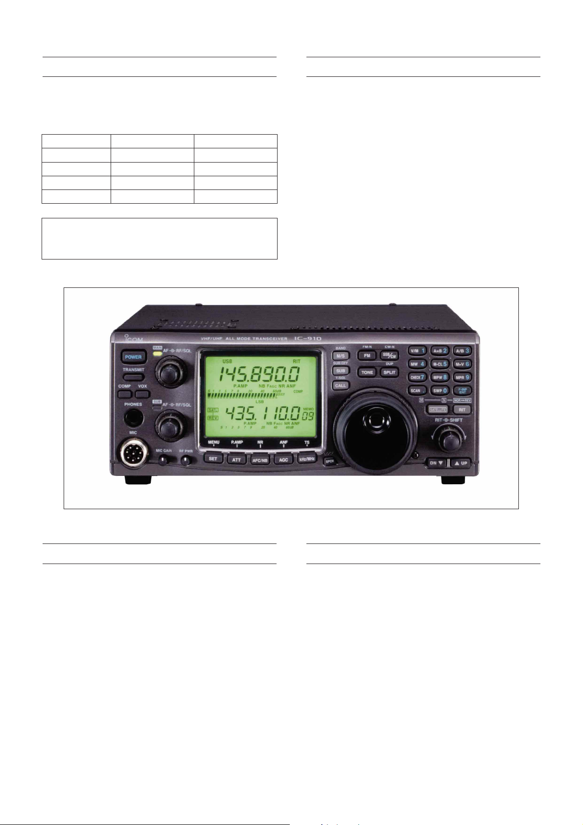
VHF/UHF ALL MODE TRANSCEIVER
i910H
Page 2
INTRODUCTION
This service manual describes the latest service information
for the IC-910H VHF/UHF ALLMODE TRANSCEIVER at the
time of publication.
VERSION No.
#02
#04
#06
#07
VERSION
Europe
Australia
U.S.A.
Korea
SYMBOL
EUR
AUS
USA-1
KOR
To upgrade quality, any electrical or mechanical parts and
internal circuits are subject to change without notice or
obligation.
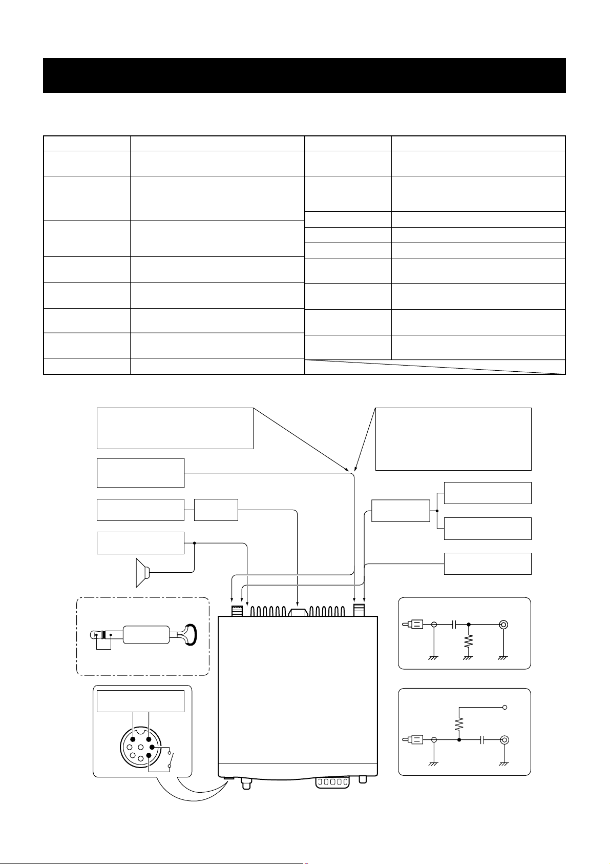
DANGER
NEVER connect the transceiver to an AC outlet or to a DC
power supply that uses more than 16 V. This will ruin the
transceiver.
DO NOT expose the transceiver to rain, snow or any liquids.
DO NOT reverse the polarities of the power supply when
connecting the transceiver.
DO NOT apply an RF signal of more than 20 dBm (100 mW)
to the antenna connector. This could damage the transceiver’s front end.
ORDERING PARTS
Be sure to include the following four points when ordering
replacement parts:
1. 10-digit order numbers
2. Component part number and name
3. Equipment model name and unit name
4. Quantity required
<SAMPLE ORDER>
1110003140 IC LA1150N IC-910H MAIN UNIT 5 pieces
8810005770 Screw BiH M3×8 ZK IC-910H Cover 10 pieces
Addresses are provided on the inside back cover for your
convenience.
REPAIR NOTES
1. Make sure a problem is internal before disassembling
the transceiver.
2. DO NOT open the transceiver until the transceiver is
disconnected from its power source.
3. DO NOT force any of the variable components. Turn
them slowly and smoothly.
4. DO NOT short any circuits or electronic parts. An insu-
lated tuning tool MUST be used for all adjustments.
5. DO NOT keep power ON for a long time when the trans-
ceiver is defective.
6. DO NOT transmit power into a signal generator or a
sweep generator.
7. ALWAYS connect a 50 dB to 60 dB attenuator between
the transceiver and a deviation meter or spectrum analyzer when using such test equipment.
8. READ the instructions of test equipment thoroughly
before connecting equipment to the transceiver.
Page 3

SECTION 1 SPECIFICATIONS
SECTION 2 INSIDE VIEWS
2 - 1 IC-910H . . . . . . . . . . . . . . . . . . . . . . . . . . . . . . . . . . . . . . . . . . . . . . . . . . . . . . . . . . . . . . . . . . . . . . . 2 - 1
2 - 2 UX-910 (OPTIONAL UNIT) . . . . . . . . . . . . . . . . . . . . . . . . . . . . . . . . . . . . . . . . . . . . . . . . . . . . . . . . . 2 - 3
SECTION 3 DISASSEMBLY AND OPTION INSTRUCTIONS
SECTION 4 CIRCUIT DESCRIPTION
SECTION 5 ADJUSTMENT PROCEDURES
SECTION 6 PARTS LIST
SECTION 7 MECHANICAL PARTS
SECTION 8 SEMI-CONDUCTOR INFORMATION
SECTION 9 BOARD LAYOUTS
9 - 1 VR-A BOARD . . . . . . . . . . . . . . . . . . . . . . . . . . . . . . . . . . . . . . . . . . . . . . . . . . . . . . . . . . . . . . . . . . . 9 - 1
9 - 2 VR-B BOARD . . . . . . . . . . . . . . . . . . . . . . . . . . . . . . . . . . . . . . . . . . . . . . . . . . . . . . . . . . . . . . . . . . . 9 - 1
9 - 3 RIT BOARD . . . . . . . . . . . . . . . . . . . . . . . . . . . . . . . . . . . . . . . . . . . . . . . . . . . . . . . . . . . . . . . . . . . . 9 - 1
9 - 4 FUNC BOARD . . . . . . . . . . . . . . . . . . . . . . . . . . . . . . . . . . . . . . . . . . . . . . . . . . . . . . . . . . . . . . . . . . 9 - 3
9 - 5 MIC BOARD . . . . . . . . . . . . . . . . . . . . . . . . . . . . . . . . . . . . . . . . . . . . . . . . . . . . . . . . . . . . . . . . . . . . 9 - 3
9 - 6 JACK BOARD . . . . . . . . . . . . . . . . . . . . . . . . . . . . . . . . . . . . . . . . . . . . . . . . . . . . . . . . . . . . . . . . . . . 9 - 3
9 - 7 DRV BOARD . . . . . . . . . . . . . . . . . . . . . . . . . . . . . . . . . . . . . . . . . . . . . . . . . . . . . . . . . . . . . . . . . . . 9 - 3
9 - 8 VARISTOR-A BOARD . . . . . . . . . . . . . . . . . . . . . . . . . . . . . . . . . . . . . . . . . . . . . . . . . . . . . . . . . . . . . 9 - 3
9 - 9 VARISTOR-B BOARD . . . . . . . . . . . . . . . . . . . . . . . . . . . . . . . . . . . . . . . . . . . . . . . . . . . . . . . . . . . . . 9 - 3
9 - 10 VARISTOR-C BOARD . . . . . . . . . . . . . . . . . . . . . . . . . . . . . . . . . . . . . . . . . . . . . . . . . . . . . . . . . . . . . 9 - 3
9 - 11 DISPLAY BOARD . . . . . . . . . . . . . . . . . . . . . . . . . . . . . . . . . . . . . . . . . . . . . . . . . . . . . . . . . . . . . . . . 9 - 5
9 - 12 PA UNIT . . . . . . . . . . . . . . . . . . . . . . . . . . . . . . . . . . . . . . . . . . . . . . . . . . . . . . . . . . . . . . . . . . . . . . . 9 - 7
9 - 13 PLL UNIT . . . . . . . . . . . . . . . . . . . . . . . . . . . . . . . . . . . . . . . . . . . . . . . . . . . . . . . . . . . . . . . . . . . . . . 9 - 9
9 - 14 MAIN UNIT . . . . . . . . . . . . . . . . . . . . . . . . . . . . . . . . . . . . . . . . . . . . . . . . . . . . . . . . . . . . . . . . . . . . 9 - 11
9 - 15 UX-910 MAIN UNIT . . . . . . . . . . . . . . . . . . . . . . . . . . . . . . . . . . . . . . . . . . . . . . . . . . . . . . . . . . . . . . 9 - 13
SECTION 10 BLOCK DIAGRAMS
10 - 1 MAIN UNIT . . . . . . . . . . . . . . . . . . . . . . . . . . . . . . . . . . . . . . . . . . . . . . . . . . . . . . . . . . . . . . . . . . . . 10 - 1
10 - 2 PA AND PLL UNITS . . . . . . . . . . . . . . . . . . . . . . . . . . . . . . . . . . . . . . . . . . . . . . . . . . . . . . . . . . . . . 10 - 2
10 - 3 FRONT UNIT . . . . . . . . . . . . . . . . . . . . . . . . . . . . . . . . . . . . . . . . . . . . . . . . . . . . . . . . . . . . . . . . . . 10 - 3
10 - 4 UX-910 . . . . . . . . . . . . . . . . . . . . . . . . . . . . . . . . . . . . . . . . . . . . . . . . . . . . . . . . . . . . . . . . . . . . . . . 10 - 3
SECTION 11 WIRING DIAGRAM
SECTION 12 VOLTAGE DIAGRAMS
12 - 1 FRONT UNIT . . . . . . . . . . . . . . . . . . . . . . . . . . . . . . . . . . . . . . . . . . . . . . . . . . . . . . . . . . . . . . . . . . 12 - 1
12 - 2 PLL UNIT . . . . . . . . . . . . . . . . . . . . . . . . . . . . . . . . . . . . . . . . . . . . . . . . . . . . . . . . . . . . . . . . . . . . . 12 - 2
12 - 3 PA UNIT (1) . . . . . . . . . . . . . . . . . . . . . . . . . . . . . . . . . . . . . . . . . . . . . . . . . . . . . . . . . . . . . . . . . . . . 12 - 3
12 - 4 PA UNIT (2) . . . . . . . . . . . . . . . . . . . . . . . . . . . . . . . . . . . . . . . . . . . . . . . . . . . . . . . . . . . . . . . . . . . . 12 - 4
12 - 5 MAIN UNIT (1) . . . . . . . . . . . . . . . . . . . . . . . . . . . . . . . . . . . . . . . . . . . . . . . . . . . . . . . . . . . . . . . . . 12 - 5
12 - 6 MAIN UNIT (2) . . . . . . . . . . . . . . . . . . . . . . . . . . . . . . . . . . . . . . . . . . . . . . . . . . . . . . . . . . . . . . . . . 12 - 6
12 - 7 MAIN UNIT (3) . . . . . . . . . . . . . . . . . . . . . . . . . . . . . . . . . . . . . . . . . . . . . . . . . . . . . . . . . . . . . . . . . 12 - 6
12 - 8 UX-910 MAIN UNIT (1) . . . . . . . . . . . . . . . . . . . . . . . . . . . . . . . . . . . . . . . . . . . . . . . . . . . . . . . . . . . 12 - 7
12 - 9 UX-910 MAIN UNIT (2) . . . . . . . . . . . . . . . . . . . . . . . . . . . . . . . . . . . . . . . . . . . . . . . . . . . . . . . . . . . 12 - 8
TABLE OF CONTENTS
Page 4

SECTION 1 SPECIFICATIONS
1 - 1
■ GENERAL
• Frequency coverage : (Unit: MHz)
*
1
Optional UX-910 is installed.
*2Guaranteed range is 144.0–148.0 MHz.
*3Guaranteed range is 430.0–450.0 MHz.
*4Guaranteed range is 1240.0–1300.0 MHz.
• Mode : USB, LSB, CW, FM, FM-N*
*Not available in 1200 MHz band
• No. of memory Ch. : 212 (99 regular, 6 scan edges, 1 calls for each band) plus 10 satellite memories)
• Antenna connector : SO-239 (50 Ω; VHF)
Type-N (50 Ω; UHF)
• Usable temp. range : –10˚C to +60˚C; +14˚F to +140˚F
• Frequency stability : Less than ±3 ppm (–10 to 60˚C; +14 to +140˚F)
• Frequency resolution : 1 Hz minimum
• Power supply : 13.8 V DC ±15% (negative ground)
• Current drain (at 13.8 V DC) :
Transmit Max. power 23.0 A
Receive Standby 2.0 A (3.0 A with UX-910)
Max. audio 2.5 A (3.5 A with UX-910)
• Dimensions : 241(W) × 94(H) × 239(D) mm
(projections not included) 9
1
⁄2(W) × 311⁄16(H) × 913⁄32(D) in
• Weight (approx.) : 4.5 kg; 10 lb (with UX-910: 5.35 kg; 11 lb 13 oz)
• ACC 1 connector : 8-pin DIN connector
• CI-V connector : 2-conductor 3.5 (d) mm (
1
⁄8″)
• DATA connectors : 6-pin mini DIN × 2 (for MAIN and SUB)
■ TRANSMITTER
• Output power : (continuously adjustable)
144 MHz 5–100 W
430 (440) MHz 5–75 W
1200 MHz 1–10 W (with UX-910)
• Modulation system : SSB Balanced modulation
FM
Variable reactance modulation
• Spurious emission : 144/430 (440) MHz More than 60 dB
1200 MHz More than 50 dB
• Carrier suppression : More than 40 dB
• Unwanted sideband : More than 40 dB
suppression
•
Microphone connector
: 8-pin connector (600 Ω)
• KEY connector : 3-conductor 3.5(d) mm (
1
⁄4″)
Version 144 MHz 430 (440) MHz 1200 MHz*
1
U.S.A.
Tx: 144.0–148.0 Tx: 430.0–450.0 Tx: 1240.0–1300.0
Rx: 136.0–174.0*
2
Rx: 420.0–480.0*
3
Rx: 1240.0–1320.0*
4
Europe 144.0–146.0 430.0–440.0 1240.0–1300.0
Australia 144.0–148.0 430.0–450.0 1240.0–1300.0
Korea 144.0–146.0 430.0–440.0 1260.0–1300.0
All stated specifications are subject to change without notice or obligation.
Page 5
■ RECEIVER
• Receive system :
VHF SSB, CW
Single conversion superheterodyne
FM
Double conversion superheterodyne
UHF SSB, CW
Double conversion superheterodyne
FM Triple conversion superheterodyne
• Intermediate frequencies : (Unit: MHz)
• Sensitivity : SSB, CW (10 dB S/N) Less than 0.11 µV
FM (12 dB SINAD) Less than 0.18 µV
• Squelch sensitivity : SSB, CW Less than 1.0 µV
(threshold) FM Less than 0.18 µV
• Selectivity : SSB, CW More than 2.3 kHz/–6 dB
Less than 4.2 kHz/–60 dB*
FM More than 15.0 kHz/–6 dB
Less than 30.0 kHz/–60 dB*
FM-N More than 6.0 kHz/–6 dB
Less than 18.0 kHz/–36 dB
CW-N More than 0.5 kHz/–6 dB
(w/FL-132 or FL-133) Less than 1.34 kHz/–60 dB*
*Except 1200 MHz band
• Spurious and image rejection ratio:
144/430 (440) MHz More than 60 dB
1200 MHz More than 50 dB
• AF output power (at 13.8 V DC):
More than 2.0 W at 10% distortion with an 8 Ω load
• RIT variable range : 144/430 (440) MHz ±1.0 kHz (SSB, CW)
±5.0 kHz (FM)
1200 MHz ±2.0 kHz (SSB, CW)
±10.0 kHz (FM)
•
IF SHIFT variable range
: More than ±1.2 kHz
• PHONES connector : 3-conductor 6.35(d) mm (1⁄4″)
• Ext. SP connectors : 2-conductor 3.5 (d) mm (1⁄8″) /8 Ω × 2 (for MAIN and SUB)
MAIN BAND SUB BAND
1st 2nd 3rd 1st 2nd 3rd
SSB 10.8500 ——10.9500 ——
CW 10.8491 ——10.9491 ——
FM 10.8500 0.455 — 10.9500 0.455 —
SSB 71.2500 10.8500 — 71.3500 10.9500 —
CW 71.2491 10.8491 — 71.3491 10.9491 —
FM 71.2500 10.8500 0.455 71.3500 10.9500 0.455
SSB 243.9500 10.8500 — 243.9500 10.9500 —
CW 243.9491 10.8491 — 243.9491 10.9491 —
FM 243.9500 10.8500 0.455 243.9500 10.9500 0.455
144 MHz
430 (440) MHz
1200 MHz
1 - 2
Page 6
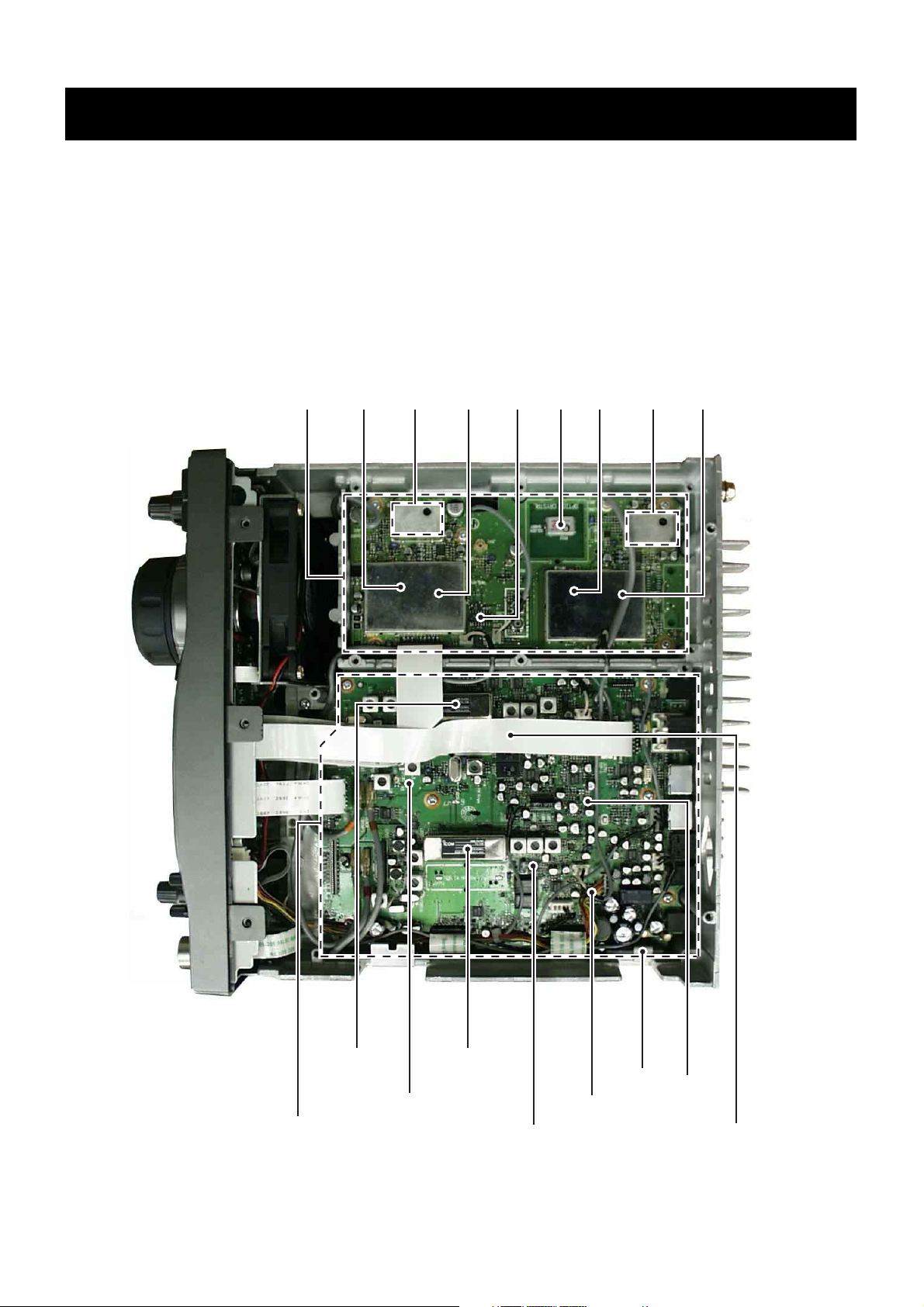
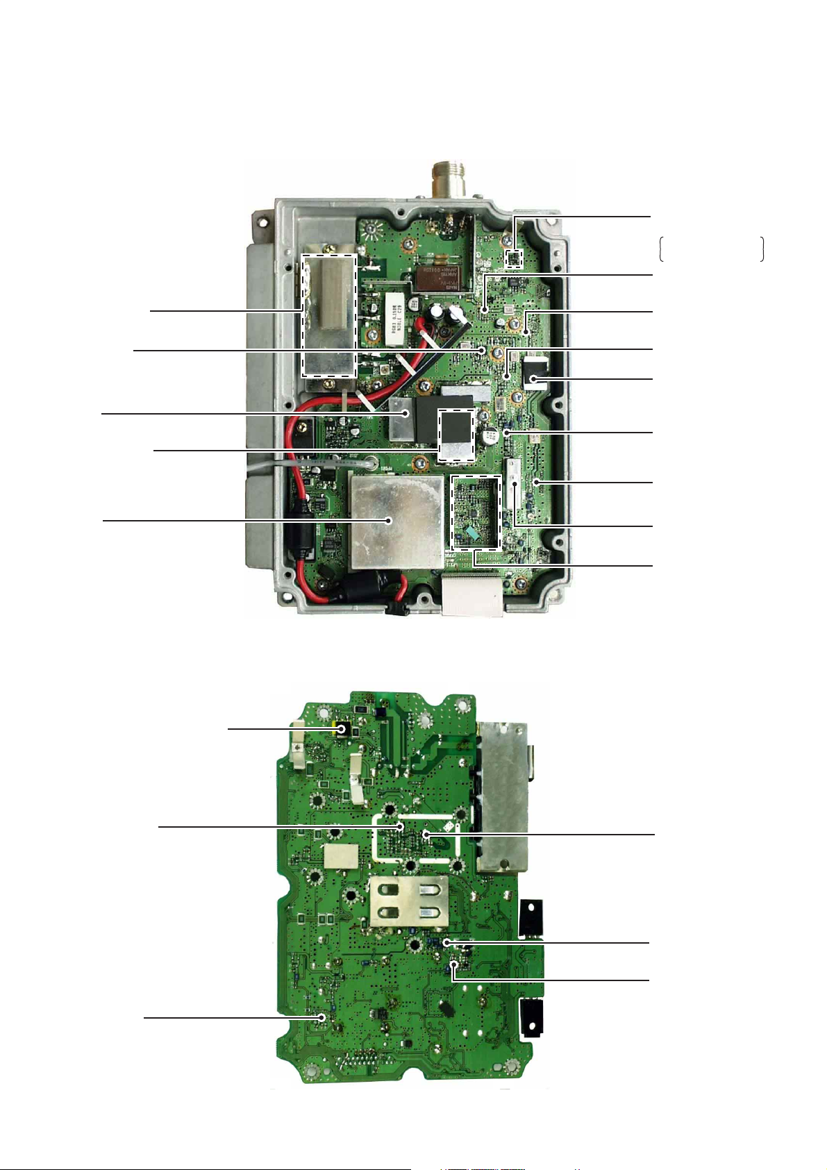
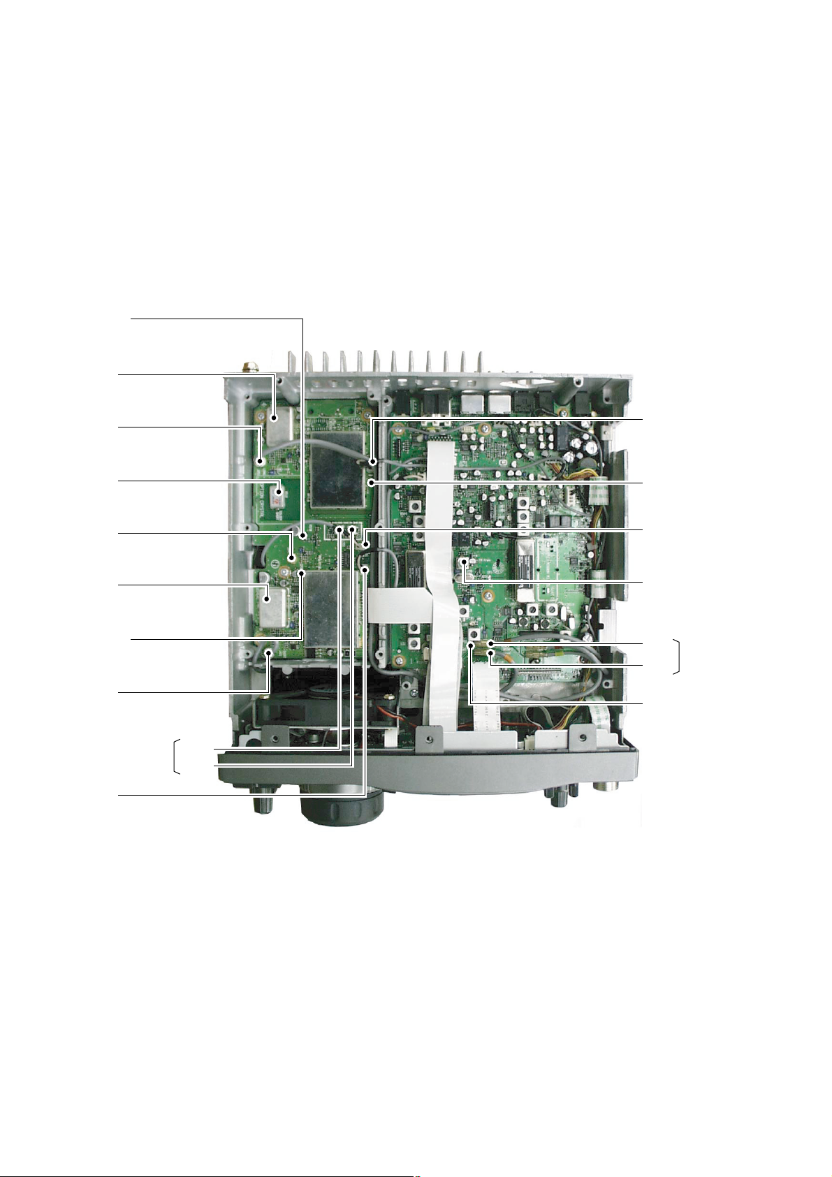
2 - 1
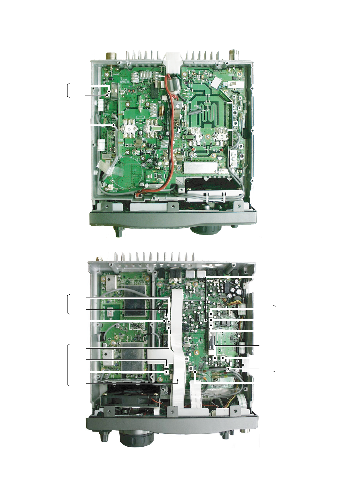
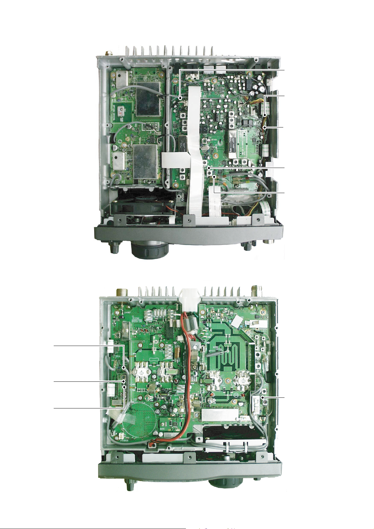
SECTION 2 INSIDE VIEWS
2-1 IC-910H
• MAIN AND PLL UNITS
DDS IC
(IC701: SC-1287)
DDS gate array
(IC131: SC-1246A)
DDS gate array
(IC331: SC-1246A)
PLL unit
144 MHz band VCO circuit
430 MHz band VCO circuit
Reference oscillator
(X512: CR-452 30.2 MHz)
Driver IC
(IC1: BU4094BCF)
DDS IC
(IC601: SC-1287)
AF power amplifier
(IC1852: LA4445)
MAIN unit
* Located under side of the point
FM IF IC
(IC951: TA31136FN)
D/A converter
(IC1521: M62352GP)
Analog master IC*
(IC1701: µPC5023-077)
FM IF IC
(IC401: TA31136FN)
Crystal band pass filter
(FI751: FL-129)
Crystal band pass filter
(FI151: FL-128)
TX IF amplifier*
(Q1: 3SK131)
Page 7
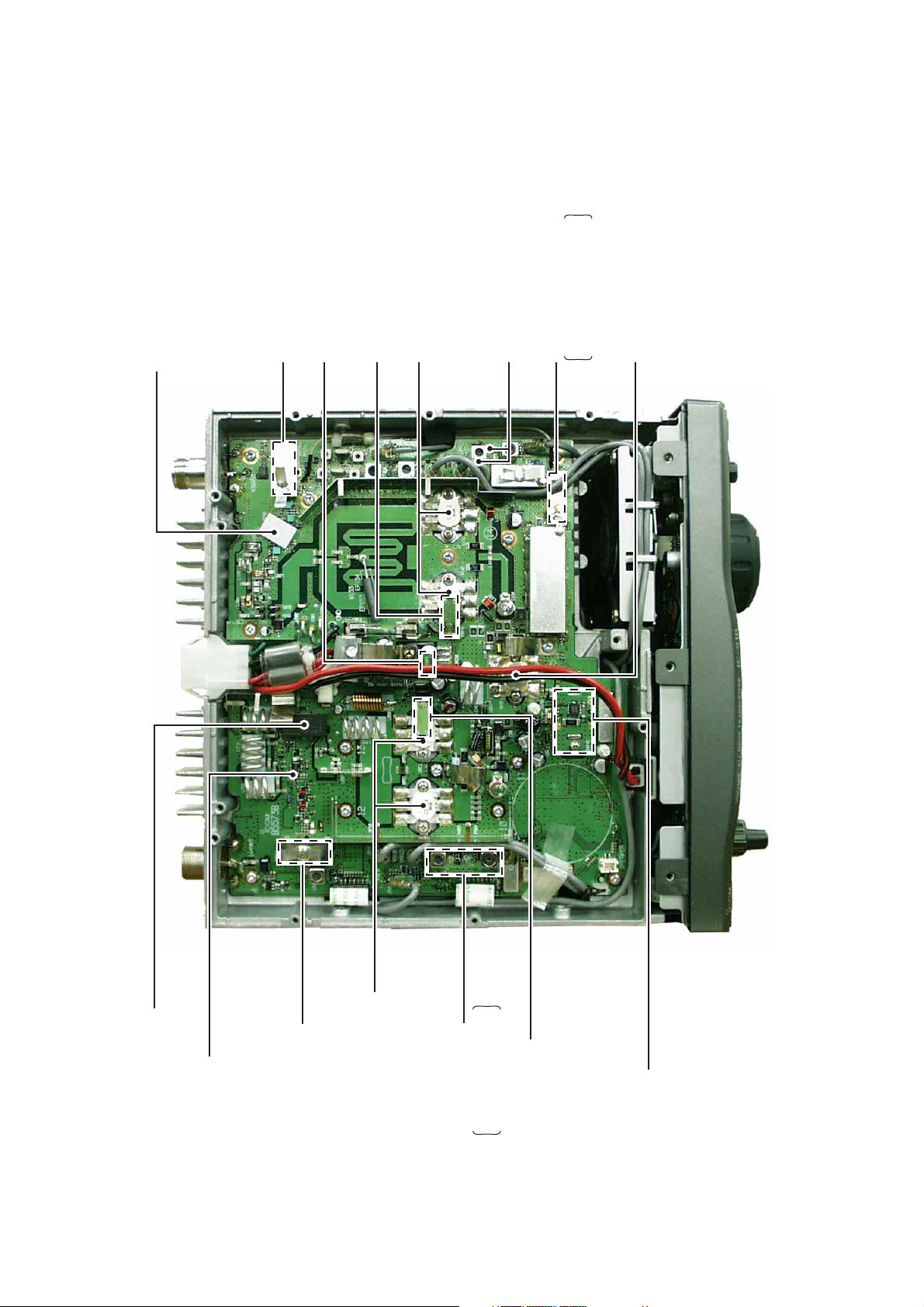
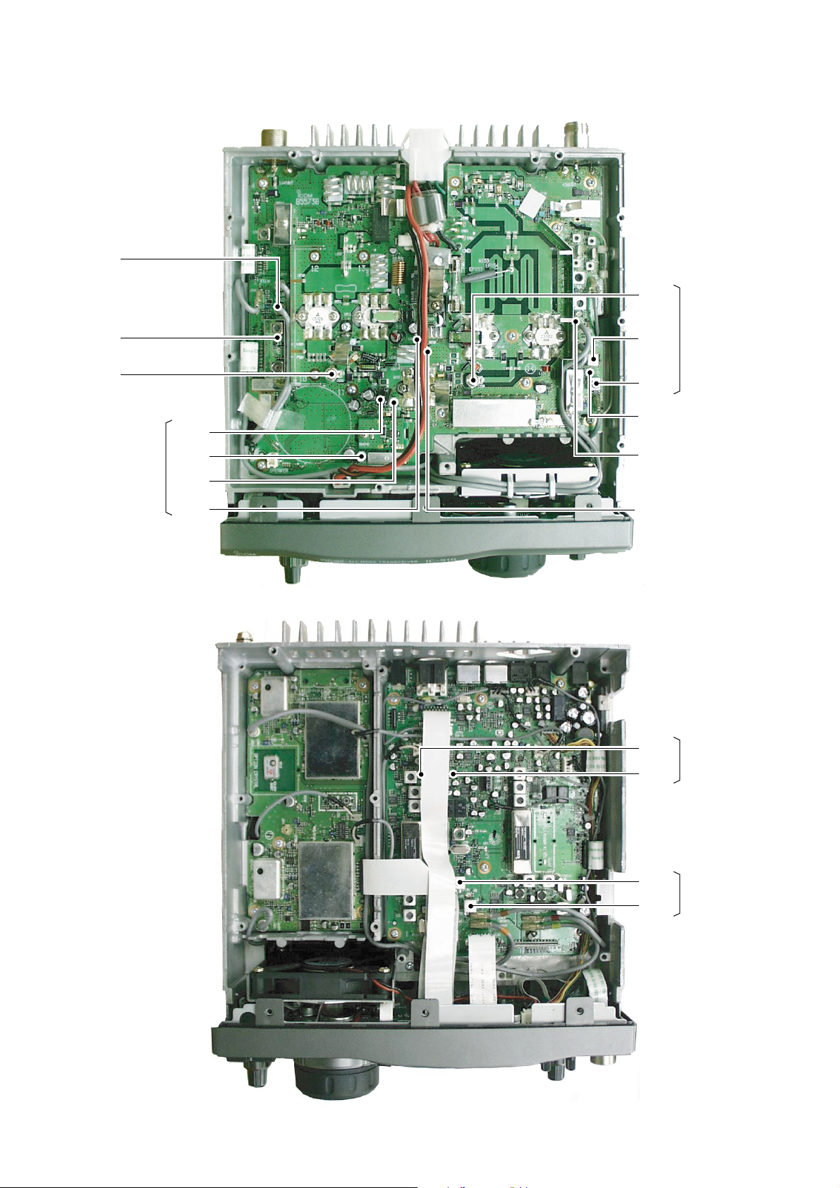
2 - 2
• PA UNIT
TX balanced mixer
Q501, Q502: 2SK302
D502: 1SV286
RX balanced mixer
(Q511, Q512: 2SK1740)
Pre-amplifier
(Q507: 3SK177)
145 MHz power amplifier
(Q651, Q652: 2SC5152)
TX/RX switching relay
(RL700: AE5349)
Varistor-A board
Varistor-C board
440 MHz power amplifier
(Q151, Q152: 2SC3102)
TX balanced mixer*
(Q1, Q2: 2SK302)
Pre-amplifier
(Q260: 3SK177)
RX balanced mixer
(Q220, Q221: 2SC3356)
DRV board
Drive amplifier
(Q131: SRFJ7044)
* Located under side of the point
Varistor-B board
TX double balanced mixer
D190: HSB88WS
L190, L191: 617DB-1010
Page 8
2 - 3
2-2 UX-910 (OPTIONAL UNIT)
• TOP VIEW
• BOTTOM VIEW
Power module IC
(IC21: M57762-02)
1st LO VCO circuit
PLL IC
(IC501: TB31242)
DDS IC
(IC661: SC-1246A)
RF pre-amplifier
(Q281: NE34018)
Power supply circuit
for AG-1200
Q72: DTC144EU
Q73, Q74: 2SC2712
RF amplifier
(Q271: 2SC5454)
YGR amplifier
(IC141: µPC1878G)
TX 1st mixer
(IC131: µPC8163TB)
RX 1st mixer
(IC241: µPC2721)
TX 1st IF amplifier
(IC111: µPC2709)
RX 2nd mixer
(Q221: 3SK166)
TX 2nd mixer
(D82: HSB88WS)
2nd LO VCO circuit
Power supply circuit for AG-1200
(Q71: 2SD1801)
Pre-drive amplifier
(Q36: 2SK2354)
2nd IF amplifier
(Q81: 2SC2712)
Divider
(IC610: TC7W74FU)
Reference amplifier
(IC601: TC7SU04F)
Drive amplifier
(Q38: 2SK2855)
Page 9
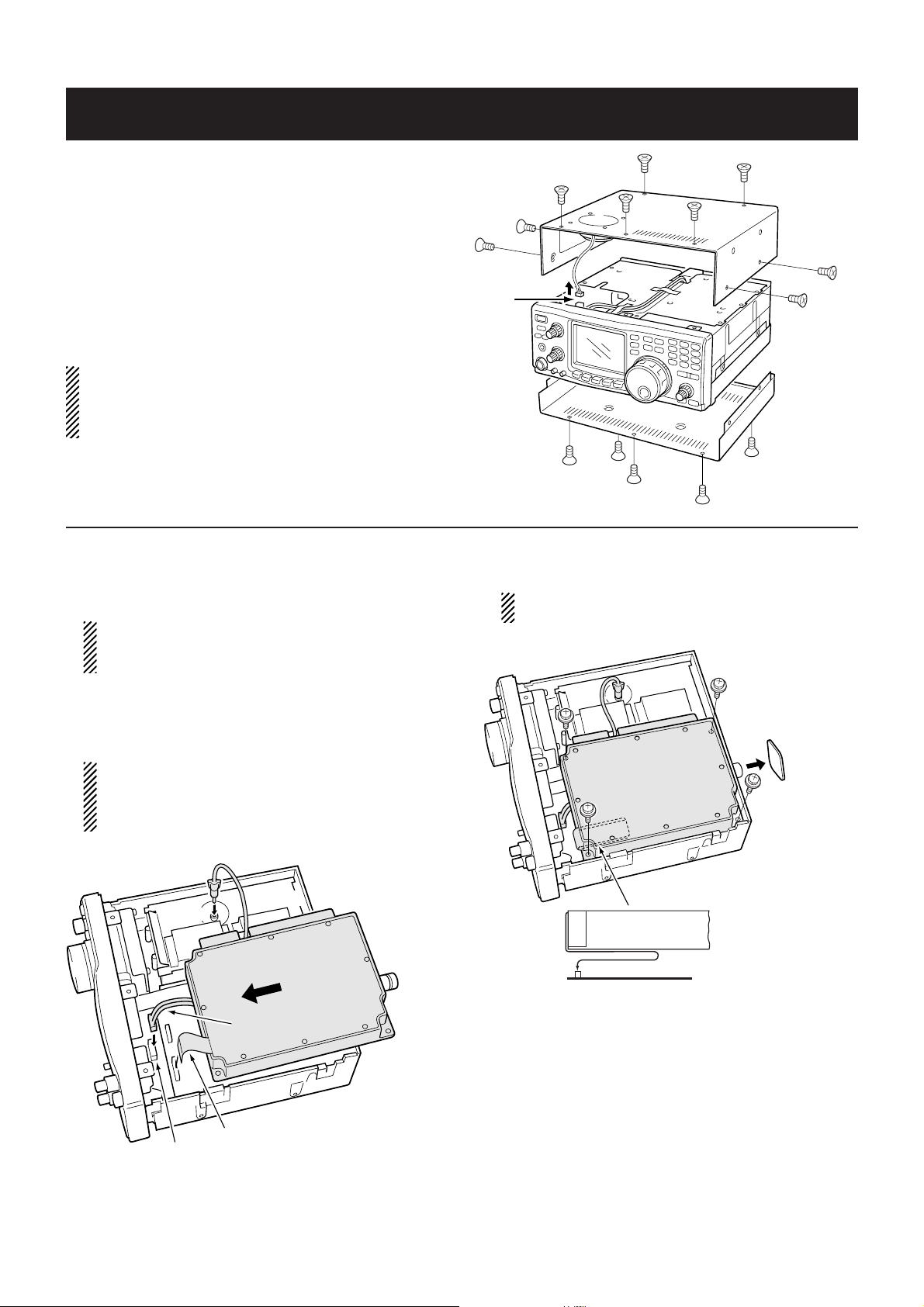
SECTION 3 DISASSEMBLY AND OPTION INSTRUCTIONS
• Opening the transceiver’s case
Follow the case and cover opening procedures
shown here when you want to install an optional unit
or adjust the internal units, etc.
q Remove the 5 screws from the top of the trans-
ceiver and 4 screws from the sides, then lift up the
top cover.
w Turn the transceiver upside down.
e Remove 5 screws from the bottom of the trans-
ceiver, then lift up the bottom cover.
CAUTION: DISCONNECT the DC power cable
from the transceiver before performing any work
on the transceiver. Otherwise, there is a danger of
electric shock and/or equipment damage.
• UX-910 1200MHz BAND UNIT
q Remove the bottom cover as shown above.
w Remove the antenna plate from the chassis using a stan-
dard screw driver.
WARNING!
NEVER attempt to remove the antenna plate using
your finger, this may result in injury.
e Connect the FFC (Flexible Flat Cable) of the
UX-910 to J2 on the MAIN unit, DC power cable to the
power connector (W305) from the PAunit and the coaxial cable to J541 on the PLL unit.
CAUTION
NEVER catch the cables from the optional DSP unit(s)
between chassis and the UX-910, this may damage
the DSP unit(s) and/or transceiver.
J541
J2
UX-910
PLL unit
Power connector
DC power cable
Coaxial cable
Flexible flat cable
Disconnect the
speaker cable.
r Place the UX-910 using the supplied 4 screws.
BE CAREFUL not to drop the supplied screws inside
the transceiver.
Antenna plate
UX-910
Turn the flexible flat cable up under the UX-910.
J2
MAIN unit
Flexible flat cable
UX-910
t Return the bottom cover to its original position.
3 - 1
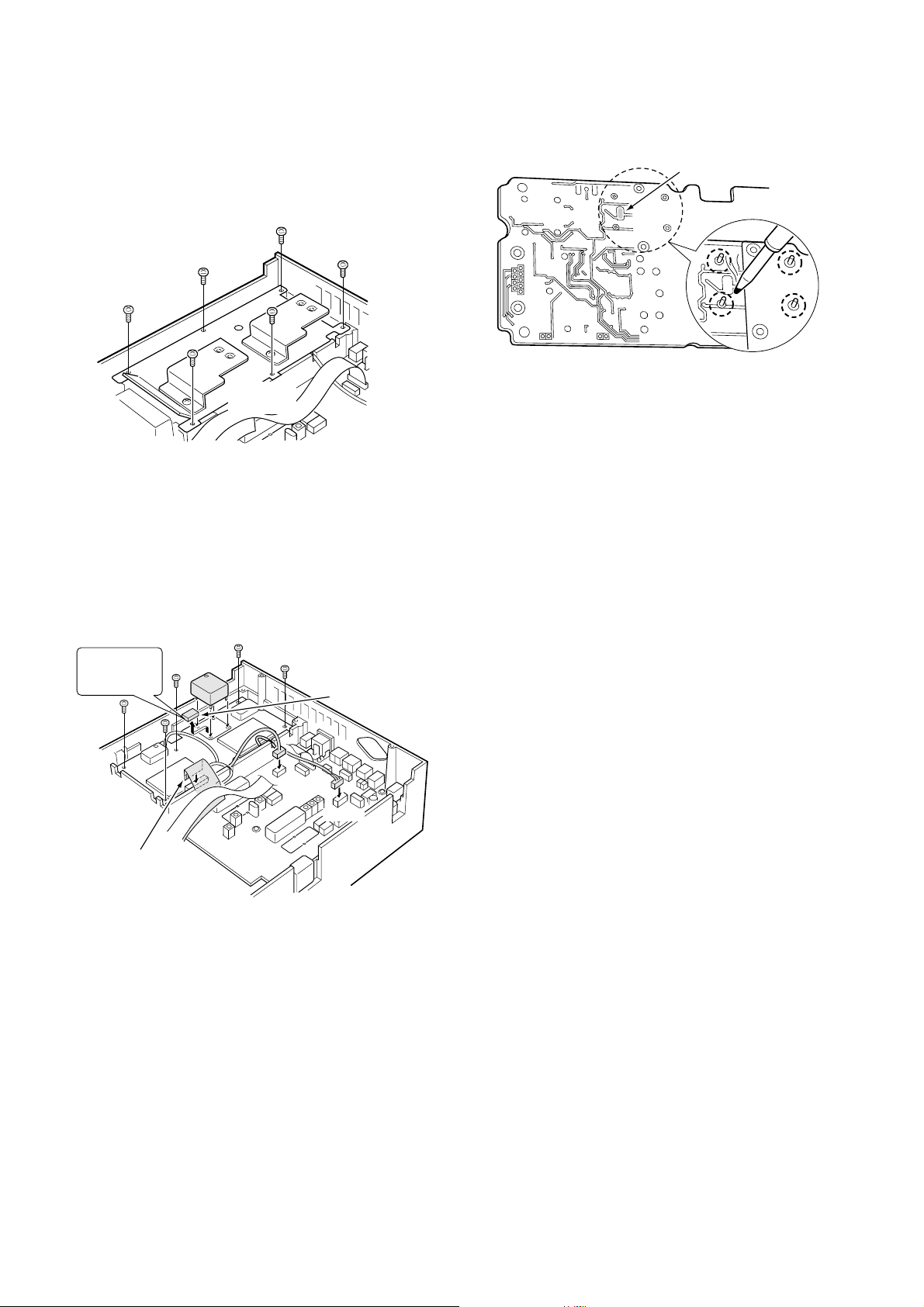
Page 10
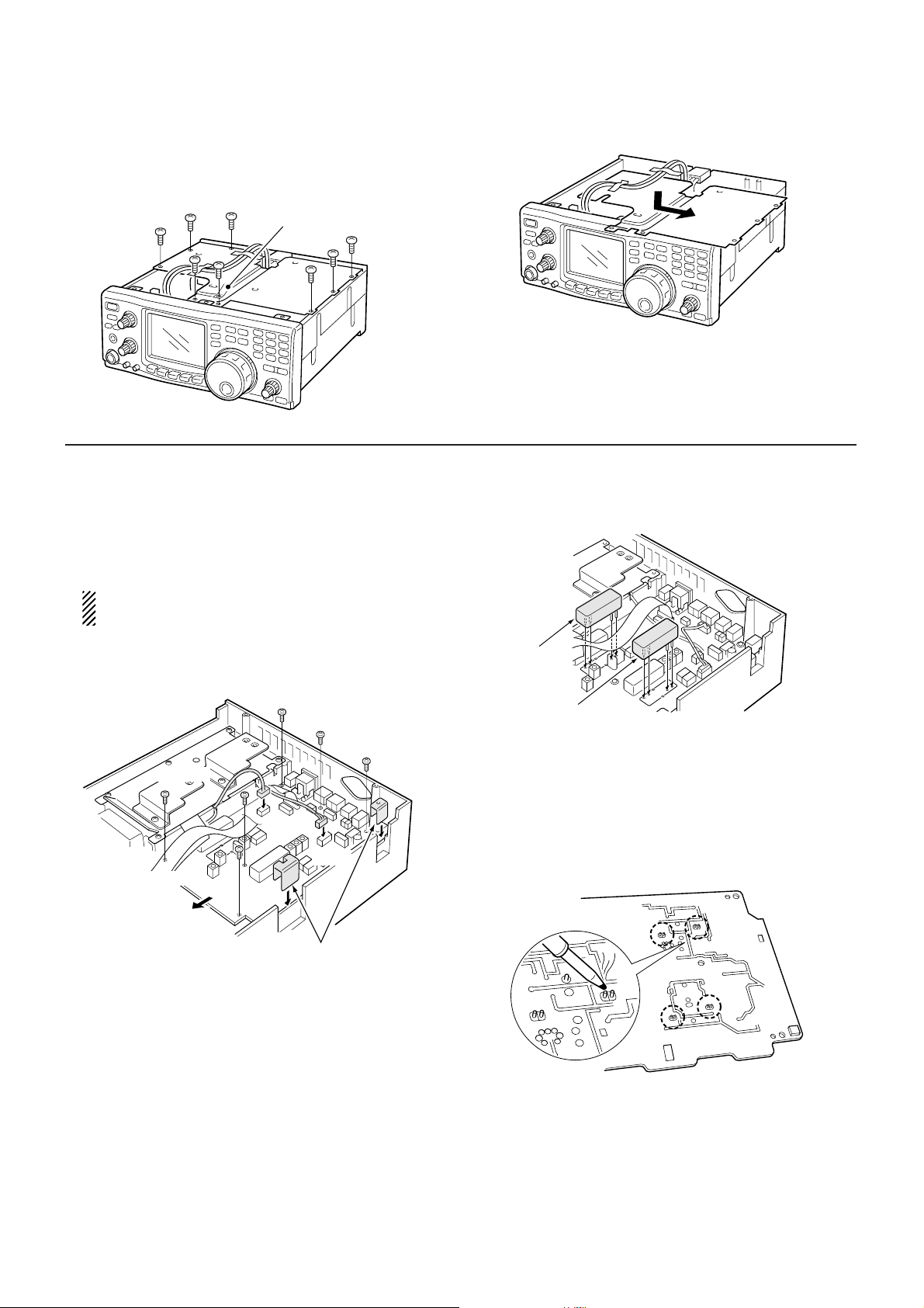
• Opening the PA unit cover
q Remove the top cover as shown in the diagram on p. 3-
1.
w Remove 8 screws and grounding plate from the PA unit
cover.
e Remove fastening tape from the inside power cable.
grounding plate
• FL-132/FL-133 CW NARROW FILTER
q Remove the bottom cover as shown in the diagram on
p. 3-1.
• Remove the UX-910 if you have installed it. (p. 3-1)
w Disconnect the connection cable connectors from J501
and J1051 on the MAIN unit.
e Remove 2 clips.
WARNING!
BE CAREFUL not to pinch your finger with the clip.
r Remove 6 screws from the MAIN unit, then lift up the
MAIN unit.
PLL unit
MAIN unit
J1051
J501
Clips
r Slide the PAunit cover as shown below.
t Install FL-132 or FL-133 to the specified position on the
MAIN unit.
FL-132
(MAIN)
FL-133
(SUB)
y Solder then cut the leads, keeping 2–3 mm (1/8’’) of the
leads from the bottom of the MAIN unit.
u Return the MAIN unit and clips to their original positions.
i Re-connect the connection cable connector to J501 and
J1051 on the MAIN unit.
o Return the bottom cover to the original position.
(MAIN)
(SUB)
3 - 2
Page 11
• UT-102 VOICE SYNTHESIZER UNIT
q Remove the bottom cover as shown in the diagram on
p. 3-1.
• Remove the UX-910 if you have installed it. (p. 3-1)
w Remove the protective paper attached to the bottom of
the UT-102 to expose the adhesive strip.
e Plug UT-102 into J1801 on the MAIN unit as shown in the
diagram at right.
r Return the bottom cover to its original position.
• UT-106 DSP UNIT
RECOMMENDATION:
When installing only 1 DSP unit, you can install into
either front or rear panel side. However, installing a
DSP unit into the front panel side may be easier and
also safer.
Installing 1st DSP unit (front panel side)
q Remove the bottom cover as shown in the diagram on
p. 3-1.
• Remove the UX-910 if you have installed it. (p. 3-1)
w Remove the shielding plate.
e Remove the connection cable from J1751 on the MAIN
unit. Connect the cable into J1 on the UT-106.
r Plug the connection cable (P1) from the UT-106 to J1751
on the MAIN unit.
t Plug the flat cable into J3 on the UT-106 and to J1771 on
the MAIN unit.
• Take care of the conductor direction.
• Attach the Velcro tape to the UT-106 and PLL unit
shielding plate.
y Return the shielding plate, top cover and bottom cover to
their original positions.
Take care of the
conductor direction.
J1771
J3
J1
J1751
Shielding plate
UT-106
MAIN unit
P1
PLL unit
Installing 2nd DSP unit (rear panel side)
q Remove the top and bottom cover as shown in the dia-
gram on p. 3-1.
• Remove the UX-910 if you have installed it. (p. 3-1)
w Remove the shielding plate.
e Remove the connection cable from J1761 on the MAIN
unit. Connect the cable into J1 on the UT-106.
UT-102
MAIN unit
J1801
The cable between J1221 on the MAIN and J1 on the
DSP unit, must be set in the groove of the chassis (see
diagram below).
Otherwise, the cable may be damaged when returning
the shield plate to its original position.
r Plug the connection cable (P1) from the UT-106 to J1761
on the MAIN unit.
t Plug the flat cable into J3 on the UT-106 and to J1781 on
the MAIN unit.
• Take care of the conductor direction.
• Attach the Velcro tape to the UT-106 and PLL unit
shielding plate.
y Return the shielding plate, top cover and bottom cover to
their original positions.
J1781
J1761
J3
J1
Shielding plate
UT-106
MAIN unit
PLL unit
Take care of the
conductor direction.
P1
J1
Set cable into the groove.
3 - 3
Page 12
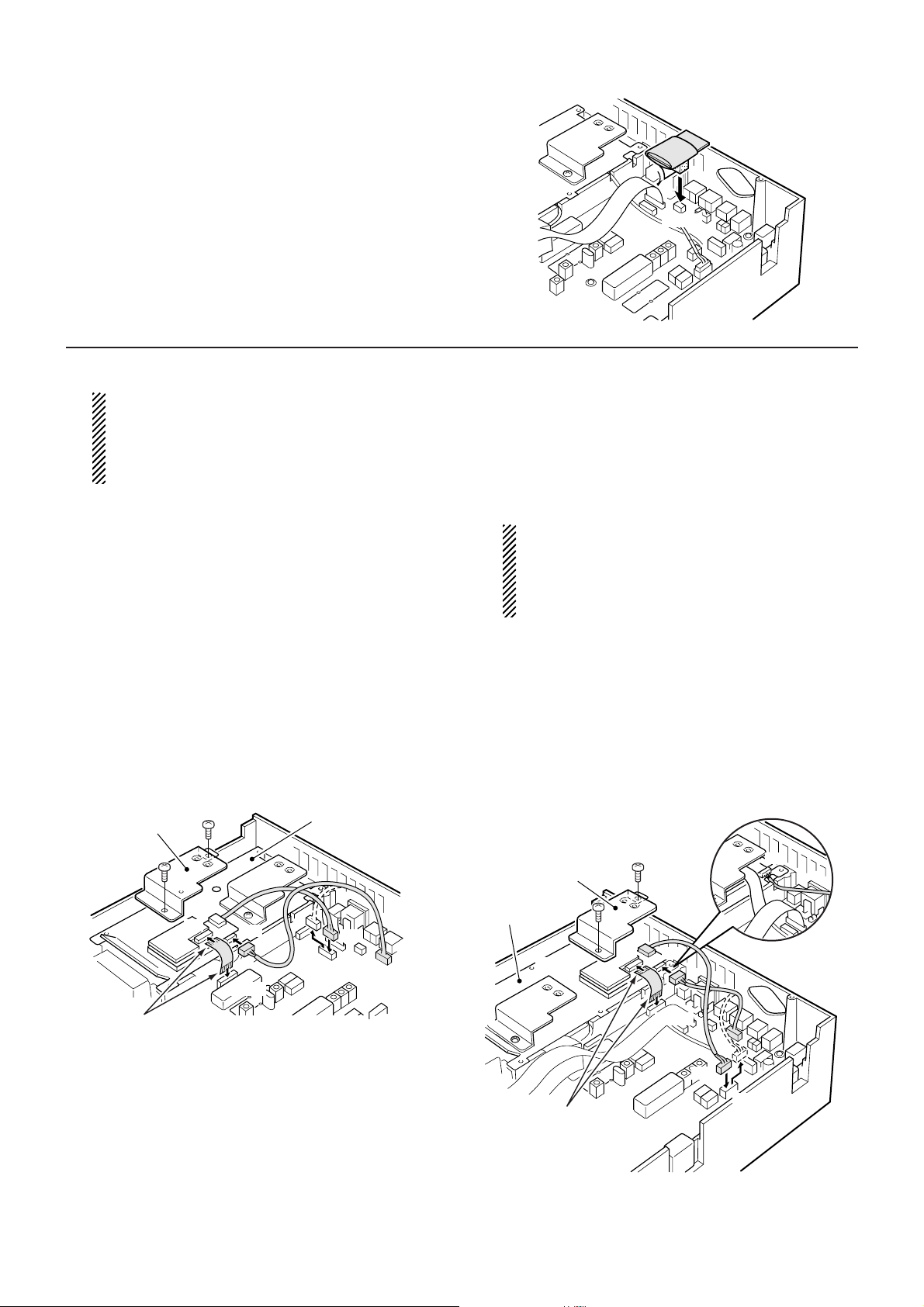
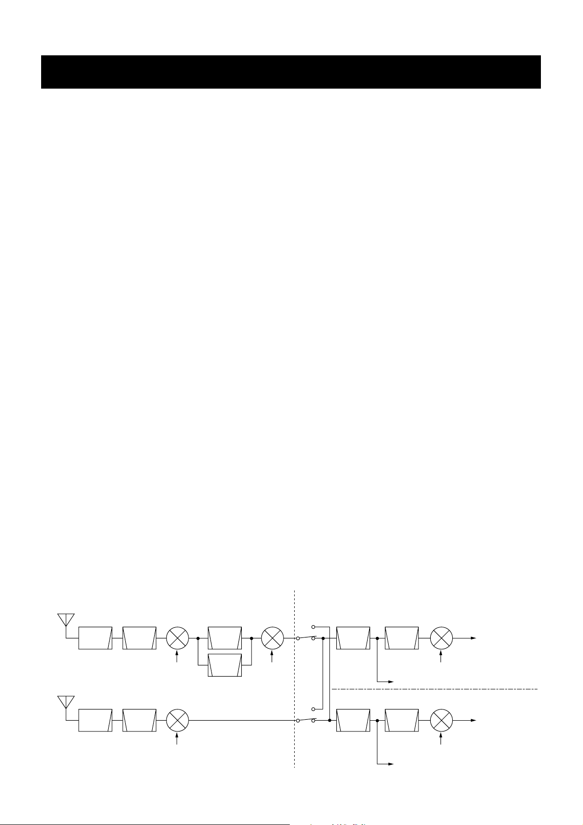
• CR-293 HIGH STABILITY CRYSTAL UNIT
q Remove the bottom cover as shown in the diagram on
p. 3-1.
• Remove the UX-910 if you have installed it. (p. 3-1)
w Remove 6 screws from the PLL shield cover, then lift up
the PLL shield cover.
PLL shield
cover
e Disconnect the FFC (Flexible Flat Cable) from the DIS-
PLAY unit and the connection cable connectors from
J501 and J1051 on the MAIN unit.
r Remove 5 screws from the PLL unit, then lift up the PLL
unit.
t Unsolder the original reference crystal, then remove it.
• The original reference crystal unit is soldered at both top
and bottom sides of the PCB (Printed Circuit Board).
J501
Original crystal
CR-293
J1051
Flexible flat cable
Unsolder the
original
crystal.
y Install the CR-293 and solder the leads.
u Return the PLL unit, PLL shield cover and bottom cover
to their original positions.
CR-293 soldering
points
Original crystal soldering point
3 - 4
Page 13
SECTION 4 CIRCUIT DESCRIPTION
4 - 1
4-1 RECEIVER CIRCUIT
Note: [Main]=Main band, [Sub]=Sub band
4-1-1 VHF TRANSMIT/RECEIVE SWITCHING
CIRCUIT (PA UNIT)
Received signals from the antenna connector (CHASSIS;
J1) are passed through the low-pass filter (L723–L721,
C728–C726, C728) then applied to the transmit/receive
switching circuit (RL700, D710).
The transmit/receive switching circuit leads receive signal to
the RF circuit from a low-pass filter while receiving.
However, the circuit leads the transmit signal from the RF
power amplifier to the antenna connector while transmitting.
The passed signals are then applied to the RF amplifier circuit.
4-1-2 VHF RF CIRCUIT (PA UNIT)
Received signals from transmit/receive switching circuit are
applied to the RF amplifier circuit (Q507) via the RF attenuator (D515), limiter (D514) and tunable band pass filter
(D513, L560) circuits.
The amplified signals are then passed through the another
three-stage tunable bandpass filters (D512–D510, L13–L15)
to suppress unwanted signals. The filtered signals are then
applied to the 1st mixer circuit (Q511, Q512).
D510–D513 employ varactor diodes, which are controlled by
the CPU (DISPLAY board; IC1) via the D/A converter (MAIN
unit; IC1521) and buffer amplifier (MAIN unit; IC1522d), to
track the bandpass filter. These varactor diodes tune the
center frequency of an RF pass band for wide bandwidth
receiving and good image response rejection.
4-1-3 VHF 1ST MIXER CIRCUIT (PA UNIT)
The 1st mixer circuit converts the received signals into a
fixed frequency of the 10 MHz IF signal with a PLL output
frequency. By changing the PLL frequency, only the desired
frequency will pass through a pair of crystal filters at the next
stage of the VHF 1st mixer.
The filtered signals from the bandpass filter are mixed with
1st LO signals at the mixer circuit (Q511, Q512) to produce
a 1st IF signal (10.85 MHz [Main] or 10.95 MHz [Sub]). The
1st LO signals (125.15 MHz–163.15 MHz) are PLL output
frequency, which comes from the VHF VCO circuit (PLL unit;
Q191, D191–D194).
The 1st IF signal is then applied to either the Main or Sub
band 10 MHz IF circuit in the MAIN unit via P501 [Main] or
P510 [Sub].
4-1-4 UHF RF CIRCUIT (PA UNIT)
The received signals from the UHF antenna connector
(CHASSIS; J2) are passed through the low-pass filter (L181,
L180, C188–C184) and then transmit/receive switching circuit (D182–D185, D265, D266, D227). The signals from the
transmit/receive switching circuit are applied to the RF
amplifier circuit (Q260) via the RF attenuator circuit (D264)
and tunable bandpass filter (D263, L288). The amplified signals are passed through the three-stage tunable bandpass
filters (D262–D260, L262–L260), and are then applied to the
1st mixer circuit (Q220, Q221).
4-1-5 UHF 1ST AND 2ND MIXER CIRCUIT
(PA UNIT)
The filtered RF signals from the bandpass filter are mixed
with a 1st LO signal at the 1st mixer circuit (Q220, Q221) to
produce a 1st IF signal (71.25 MHz [Main] or 71.35 MHz
[Sub]). The 1st IF signal is passed through a crystal filter
(Fl280 [Main], Fl281 [Sub]) to suppress out-of-band signals.
The filtered IF signal is applied to the 2nd mixer circuit (Q11)
to produce a 10 MHz IF signal (10.85 MHz [Main] or 10.95
MHz [Sub]) with a 2nd LO signal. The IF signal is then
applied to the MAIN unit via P1 [Main] or P30 [Sub].
The 1st LO signal (348.75 MHz–408.75 MHz) is generated
at the UHF VCO circuit (PLL unit; Q391, D391–D394), and
a 2nd LO signal (60.2 MHz) is produced at the PLL circuit by
doubling it’s reference frequency (30.2 MHz).
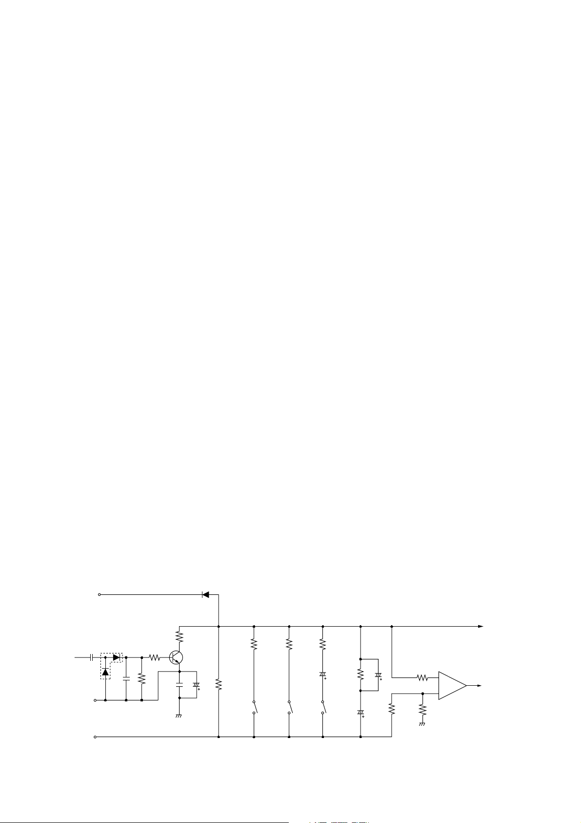
• RECEIVER CONSTRUCTION
430 MHz
1st mixer
Q220, Q221
1st LO
B1LO
2nd mixer
Q11
AF signals to
AF selector circuit
(IC452)
2nd LO
B2LO
LPF BPF BPF BPF
BPF
IC351FI51 FI151
BFOM
to FM IF IC (IC401)
BPF
144 MHz
1st mixer
Q511, Q512
1st LO
A1LO
AF signals to
AF selector circuit
(IC1002)
LPF
BPF BPF
IC851FI651 FI751
BFOM
to FM IF IC (IC951)
BPF
for MAIN band
for SUB band
10.95 MHz
10.85 MHz
MAIN unitPA unit
Page 14

4 - 2
4-1-6 10 MHz IF CIRCUIT (MAIN UNIT)
The 10 MHz IF signal from the mixer circuit is passed
through a monolithic filter (Fl51 [Main], Fl651 [Sub]) to suppress out-of-band signals. The filtered signal is amplified at
the IF amplifier (Q51 [Main], Q651 [Sub]). The IF amplifier
provides 20 dB gain.
The amplified signal is then applied to the different circuits
depending on the selected mode.
(1) FM mode
The signal is applied to an FM IF IC pin 16 (IC401 [Main] or
IC951 [Sub]).
(2) SSB and CW mode
The signal is passed through a 10 MHz IF filter (FI151/10.85
MHz [Main] or Fl751/10.95 MHz [Sub]) or optional CW narrow filters. The filtered signal is amplified at the IF amplifiers
(Q350–Q352 [Main] or Q850–Q852 [Sub]) and then applied
to a demodulator circuit.
4-1-7 DEMODULATOR CIRCUIT (MAIN UNIT)
(1) FM mode
The 10 MHz IF signal from an IF amplifier (Q51 [Main] or
Q651 [Sub]) is applied to the mixer section of the FM IF IC
(IC401 [Main], IC951 [Sub], pin 16), and is mixed with a LO
signal (10.395 MHz [Main], 10.495 MHz [Sub]) to produce a
455 kHz IF signal. The LO signal is generated by the BFO
circuit (PLL unit; IC601 [Main], IC701 [Sub]).
The FM detector circuit employs the quadrature detection
method, which uses a ceramic discriminator (X401 [Main],
X951 [Sub]) for phase delay to obtain a non-adjusting circuit.
The detected signals are output from pin 9, and applied to
the squelch control and center indication detector circuits,
etc.
(2) SSB and CW modes
The amplified signal from the IF amplifier circuit (Q51 [Main],
Q651 [Sub]) is applied to the balanced mixer circuit (IC351
[Main], IC851 [Sub]) to demodulate into AF signals.
Demodulated audio signals are output from pin 1, and
applied to the squelch control gate (IC452 [Main], IC1002
[Sub]).
BFO circuit (PLL unit; IC601 [Main] and IC701 [Sub]) generates BFO signals for using in the balanced mixers.
4-1-8 SQUELCH CONTROL CIRCUIT (MAIN UNIT)
The demodulated AF signals from the balanced mixer circuit
or FM IF IC are applied to the squelch control gate (IC452
[Main], IC1002 [Sub]). This consists of 4 analog switches
which are selected with a mode signal and squelch control
signal from the CPU (DISPLAY board; IC1) via the expander
IC (IC1491). The switched AF signals are applied to the AF
circuit.
4-1-9 SQUELCH CIRCUIT (MAIN UNIT)
(1) FM mode
A squelch circuit cuts out AF signals when no RF signal is
received or the S-meter signal is lower than the [SQL] control setting level. By detecting noise components in the AF
signals, the CPU switches the squelch control gate.
A portion of the AF signals from the FM IF IC pin 9 (IC401
[Main], IC951 [Sub]) passes through the active filter section
of FM IFIC (pin 8). The active filter section amplifies and filters noise components. The filtered signals are applied to
the noise detector section for conversion into DC voltage
and output from pin 14 (IC401 [Main], IC951 [Sub]) as the
“NSQM [Main]/NSQS [Sub]” signal. The “NSQM [Main]/
NSQS [Sub]” signal is applied to the DISPLAY board.
The DC voltages are passed through the analog multiplexer
(DISPLAY board; IC5, pins 15 and 2) and then applied to the
CPU (DISPLAY board; IC1, pins 93, 94) via the MP1Y and
MP1X signal lines. The [SQL] level signal is also applied to
the CPU via the analog multiplexer (DISPLAY board; IC3,
pins 14, 5) as a reference voltage for comparison with the
noise signals. Also, an S-meter signal is applied to the CPU
from FM IF IC pin 12 (IC401 [Main], IC951 [Sub]) via the
meter amplifier (IC1804c [Main], IC1804a [Sub]) and analog
multiplexer (DISPLAY board; IC4, pins 12 and 1). The CPU
compares these signals, then outputs a control signals to
the squelch control gate.
(2) SSB and CW modes
The squelch circuit mutes audio output when the S-meter
signal is lower than the [SQL] control setting level.
A portion of the 10 MHz IF signal from the IF amplifier (Q352
[Main], Q852 [Sub]) is converted into DC voltage at the AGC
detector (D303, Q305 [Main], D902 Q901 [Sub]) and amplified at the meter amplifier (IC1804d [Main] or IC1804b
[Sub]). The amplified signal is passed through the analog
multiplexer (DISPLAY board; IC4, pins 12 and 1) via the
SMLM [Main]/ SMLS [Sub] signals and then applied to the
CPU (DISPLAY board; IC1). The CPU outputs control signals to the squelch control gate when the S-meter signal is
low level.
4-1-10 AF AMPLIFIER CIRCUIT (MAIN UNIT)
The AF amplifier circuit amplifiers the demodulated signals
to drive a speaker. For the separate speaker function, a
stereo power amplifier is used.
AF signals from the squelch control gate are passed through
the AF filter (IC451a [Main], IC1001a [Sub]) and AF preamplifier (IC451b [Main], IC1001b [Sub]) and then amplified
at the voltage controlled amplifier (VCA: IC1808 [Main],
IC1809 [Sub]) which functions as a volume control using the
[AF] control signal. The amplified AF signals are applied to
the AF power amplifier circuit (IC1852, pin 2 [Main], pin 5
[Sub]).
The amplified audio signals of SUB band are output from pin
7, and are applied to the external speaker jack for the SUB
band (J1852) via the [PHONE] jack (JACK board; J1). When
no plug is connected to the jack, the signals are fed back to
the MAIN band audio. The mixed audio is applied to the
internal speaker via the [PHONE] jack and external speaker
jack for the MAIN band (J1851).
• BFO frequencies
Mode for MAIN band for SUB band
USB
LSB
CW
10.8485 MHz
10.8515 MHz
10.8483 MHz
10.9485 MHz
10.9515 MHz
10.9483 MHz
Page 15
4 - 3
4-1-11 NOISE BLANKER CIRCUIT (MAIN UNIT)
The noise blanker circuit detects pulse-type noises, and
stops IF amplifier operation during detection.
A portion of the 10 MHz IF signal from the bandpass filter
(FI51 [Main], FI651 [Sub]) is amplified at the noise amplifier
circuit (Q102, IC101, Q101 [Main], Q702, IC701, Q701
[Sub]). The amplified signal is rectified at the noise detector
(D371 [Main], D701 [Sub]) for conversion into DC voltage.
The DC voltage is amplified at the DC amplifier circuit (Q105
[Main], Q705 [Sub]) and then applied to the noise blanker
control circuit (Q52, Q107 [Main], Q652, Q707 [Sub]) to stop
amplification of the IF amplifier circuit (Q51 [Main], Q651
[Sub]).
4-1-12 AGC CIRCUIT (MAIN UNIT)
The AGC (Auto Gain Control) circuit reduces IF amplifier
gain to keep the audio output at a constant level.
A portion of the 10 MHz IF signal from the IF amplifier (Q352
[Main], Q852 [Sub]) is applied to the AGC detector circuit
D303 [Main], D902 [Sub]). The detected signal is then amplified at the DC amplifier circuit (Q305 [Main], Q901 [Sub])
and then applied to the IF amplifiers (Q51, Q351, Q352
[Main], Q651, Q851, Q852 [Sub]).
When strong signals are received, the detected voltage
increases and the output level of the DC amplifier, as AGC
voltage, decreases. The AGC voltage is used for the bias
voltage for the IF amplifiers, therefore, the IF amplifier gain
is decreased.
AGC response time is controlled by changing the time constant at the AGC control line with a resistor and capacitor.
While AGC is set to slow, the resistor (R312 [Main], R914
[Sub]) and capacitor (C306 [Main], C911 [Sub]) are connected to the AGC control line. While AGC is set to fast,
R311 [Main], R913 [Sub] are connected to the AGC control
line. Due to Q304 and Q303 [Main]/Q905 and Q904 [Sub]
being switched ON that controlled by the “AGSM”, “AGFM”
[Main], “AGSS”, “AGFS” [Sub]. Also, R310 [Main]/R912
[Sub] is connected to the AGC control line due to Q302
[Main]/Q903 being switched ON while scanning for faster
response than AGC fast mode that controlled by the
“AGRM” [Main], “AGRS” [Sub].
4-1-13 S-METER CIRCUIT (MAIN UNIT)
The S-meter circuit indicates the relative received signal
strength while receiving and changes depending on the
received signal strength.
(1) FM mode
Some of the amplified IF signal is applied to the S-meter
detector section in the FM IF IC (IC401 [Main], IC951 [Sub])
to be converted into DC voltage. The converted signal is output from pin 12 and applied to the meter amplifier circuit
(IC1804c [Main], IC1804a [Sub]). The amplified signal is
then applied to the CPU (DISPLAY board; IC1) passing
through the analog multiplexer (DISPLAY board; IC4, pins
12 and 1) via the “SMLM [Main]/SMLS [Sub]” line. The CPU
then outputs S-meter control signal.
(2) SSB and CW modes
A portion of the AGC control signal is applied to the meter
amplifier (IC1804d [Main], IC1804b [Sub]). The amplified
signal is then applied to the CPU via the analog multiplexer
to control the S-meter.
4-2 TRANSMITTER CIRCUITS
4-2-1 MICROPHONE AMPLIFIER CIRCUIT
(MAIN UNIT)
The microphone amplifier circuit amplifies audio signals
from the microphone or ACC connector and then applies
them to the FM modulation or balanced modulator circuit.
One microphone amplifier circuit is commonly used for both
FM/SSB and VHF/UHF.
Audio signals from the [MIC] connector enter the microphone amplifier IC (IC1701, pin 22) and are then amplified
at the microphone amplifier or speech compressor section.
Compression level is adjusted by the setting mode.
The amplified or compressed signals are applied to the VCA
section of IC1701. The microphone gain setting from the D/A
converter (IC1521, pin 8) is applied to the VCA control terminal (IC1701, pin 10). The resulting signals from pin 9 are
then applied to the buffer-amplifier (Q1651) via the analog
switch (IC1653a). External modulation input from the [ACC]
socket (pin 4) is also applied to Q1651.
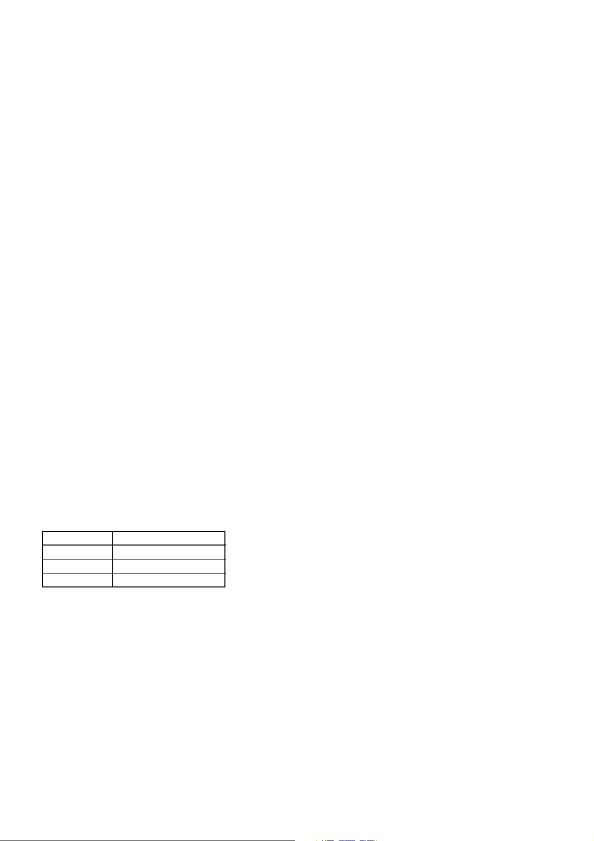
• AGC CIRCUIT FOR MAIN BAND
AGC line
RFGM
(RF/SQL control)
SLOW
Q306
9 V
–5 V
D303
C309
2nd IF
signal
C306 R312Q304
FAST
C307
R313
C308
R310Q302
C311
C310
C312
R303
R317
R304
R311Q303
D302
R316
R314
R302
Meter
amp.
IC1804d
“SMLM”
AGC det.
S-meter signal
+
–
12
14
13
SCAN
R315
Page 16
4 - 4
While in SSB mode, the amplified signals from the buffer
amplifier (Q1651) are then applied to the balanced modulator (IC201).
While in AM/FM mode, the amplified signals from the buffer
amplifier (Q1651) are applied to the limiter amplifier
(IC1651b) and splatter filter (IC1651a). The signals are
passed through the buffer amplifier ((IC1652a) and are then
applied to the AM detector (IC1807d, D1652) in AM mode or
to the varactor diode (D253) in FM mode.
4-2-2 MODULATION CIRCUIT (MAIN UNIT)
(1) FM mode
The amplified audio signals from IC1701 are pre-emphasized and limited at IC1651b and then passed through the
splatter filter (IC1651a). The filtered signals are then applied
to the FM modulation circuit (D253) via the FM deviation
level controller (IC1803 pins 21, 22) and buffer amplifier
(IC1652a). Also, subaudible tone signals from the CPU
(DISPLAY board; IC1 pin 4) are applied to the FM modulation circuit (D253) via the splatter filter (IC1651a).
The FM modulation circuit changes the generating frequency of the FM local oscillator (Q254, X251) to generate an FM
signal. The modulated IF signal is passed through the RF
limiter (Q253) and then applied to the transmit IF amplifier
circuit.
When 9600 bps mode is selected, audio signals from the
ACC connector bypass the amplifiers and are applied to
IC1654a directly via the external modulation switch (IC1531,
pins 12, 1). In such cases, the deviation detector (IC1807d)
cuts off the audio line when over modulation is detected.
(2) SSB and CW modes
The amplified audio signals from Q1651 are mixed with BFO
signals at the balanced mixer circuit (IC201) to produce a 10
MHz IF signal. The mixed signal is still a DSB signal, therefore, the mixed signal passes through bandpass filter circuit
(FI151) to suppress unwanted side band signals. The filtered signal is applied to the transmit IF amplifier circuit
4-2-3 CW KEYING CIRCUIT (MAIN UNIT)
When the CW key is closed, control signal is output from
CPU (LOGIC unit) and controls break-in operation, the side
tone signal.
Keying signals (DOT and DASH) from the [KEY] jack
(J1401) are applied to the CPU (DISPLAY board; IC1, pins
49, 48 respectively), and the CPU outputs a CW control signal (KDS1) from pin 21. The CW control signal is applied to
the balanced mixer (IC201) via Q201, D201, D207 to unbalance the IC201 input bias voltage and creates a carrier signal. R202 determines the transmit delay timing.
4-2-4 TRANSMIT IF AMPLIFIER CIRCUIT
(MAIN UNIT)
The modulated IF signal from a modulation circuit is applied
to the IF amplifier circuit (Q1). The amplified IF signal is then
applied to the VHF/UHF transmit circuit (PA unit) via the VHF
/UHF switching circuit (D52, D53).
The gain of the IF amplifier circuit (Q1) is controlled by the
ALC amplifier circuit (IC1601b). Therefore, the IF amplifier
is reduced when the output power increases.
4-2-5 RF CIRCUIT (PA UNIT)
The RF circuit consists of mixer and drive amplifiers to
obtain the desired frequency and level needed at a PA circuit, respectively.
(1) VHF band
The IF signal from the MAIN unit (P501) is mixed with an LO
signal from the VHF VCO circuit (PLL unit; Q191,
D191–D194) at the double-balanced mixer circuit (Q501,
Q502, D502) to be converted into VHF transmit frequency.
The mixed signal is passed through the attenuator
(R512–R514) and two-stage tunable bandpass filter (D503,
L533 and D504, L504) to suppress spurious components.
The filtered signals are then amplified at the YGR amplifier
(IC501) and passed through the attenuator (R562–R531)
and another two-stage tunable bandpass filter (D641, L641
and D642, L642)
The amplified and filtered RF signal is applied to the drive
amplifier circuit that is used VHF and UHF signals commonly.
(2) UHF band
The IF signal from the MAIN unit (P1) is mixed with a 2nd LO
signal at the double-balanced mixer circuit (Q1, Q2) to produce a 2nd IF signal (71.25 MHz). The 2nd LO signal (60.4
MHz) is generated at the reference oscillator and doubler
circuit (PLL unit; X512, Q551) via LO amplifier (IC40). The
2nd IF signal is amplified at the buffer amplifier (Q3) via the
bandpass filter circuit (L3, L4, C12, C13, C15–C17, C24,
C26). The amplified 2nd IF signal is applied to the 1st mixer
circuit (D190, L190, L191) passing through the attenuator
(R12–R14) and low-pass filter (L381, L382, C381–C383).
The 1st mixer circuit (D190, L190, L191) converts the 2nd IF
signal into a UHF transmit frequency with a 1st LO signal
from the UHF VCO circuit (PLL unit; Q391, D391–D394).
The converted RF signal is passed through the bandpass filter (FI200 and FI201) where unwanted LO signal emission
is reduced. The filtered signal is attenuated at R204–R206
and amplified at the YGR amplifier (IC200), and is then
applied to the drive amplifier circuit via the band pass filter
(FI202) and another YGR amplifier (Q200).
4-2-6 DRIVE AMPLIFIER CIRCUIT (PA UNIT)
The drive amplifier circuit amplifies RF signals from the VHF
or UHF RF circuit to obtain a level needed at the power
amplifier circuit. One drive amplifier circuit is commonly used
for both VHF and UHF band signals.
The signals from the VHF or UHF RF circuit are amplified at
the drive amplifier circuit (Q101, Q121, Q131, DRV board;
Q930). The amplified VHF signals are passed through the
• Transmit IF frequencies
Mode Transmit IF signal
USB
LSB
CW
10.8485 MHz
10.8515 MHz
10.8491 MHz
Page 17

4 - 5
low-pass filter and UHF signal are high-pass filter, and then
applied to the VHF and UHF power amplifier circuit separately.
4-2-7 POWER AMPLIFIER CIRCUIT (PA UNIT)
The power amplifier circuit amplifies the RF signals to the
specified output power.
(1) VHF power amplifier circuit
The RF signal from the low-pass filter circuit is applied to the
VHF power amplifier circuit (Q651, Q652) to obtain a stable
100 W of RF output power. The amplified RF signal is
applied to the antenna connector (CHASSIS; J1) via the
power detector (D720, D721), transmit/receive switching
relay (RL700) and low-pass filter (L723–L721, C728–C726,
C728) circuits.
(2) UHF power amplifier circuit
The RF signal from the high-pass filter is applied to the
UHF power amplifier circuit (Q151, Q152) to obtain a stable 75 W of RF output power. The amplified RF signal is
applied to the antenna connector (CHASSIS; J2) via the
transmit/receive switching circuit (D182–D185), low-pass
filter (L181, L180, C188–C184) and power detector (D180,
D181) circuits.
4-2-8 ALC CIRCUIT (PA AND MAIN UNITS)
The ALC (Automatic Level Control) circuit protects the
power amplifiers (PA unit; Q651, Q652 for VHF and Q151,
Q152 for UHF) from a mismatched output load. Also, the
ALC circuit controls the gain of the transmit IF amplifier in
order for the transceiver to output even when the supplied
voltage shifts, etc.
The RF power level is detected at the power detector circuit
(PA unit; D720–D721 for VHF, D180, D181 for UHF) to be
converted into DC voltages. The detected voltage (VFOR for
VHF or UFOR for UHF) is passed through the switching
diode, and are then applied to the differential amplifier
(MAIN unit; IC1601b) via the FOR line. A reference voltage
(POCV) for IC1601b is controlled by the [RF PWR] control
to output reference voltages. The output voltage is applied
to the transmit IF amplifier circuit (MAIN unit; Q1) as an ALC
signal to control the amplifier gain.
When the VFOR/UFOR voltage increased, the output from
the differential amplifier will be decrease to reduce the IF
amplifier gain. This adjusts the RF output power until the
VFOR/UFOR and POCV voltage are well balanced.
4-2-9 APC CIRCUIT (MAIN UNIT)
The APC (Automatic Power Control) circuit protects the
power amplifiers on the PA unit from excessive current.
Current drain of power amplifiers is detected by voltage
drops at a resistor (PA unit; R305) between VCC and PAHV
lines. The original voltage (ICH) and dropped voltage (ICL)
are applied to the APC differential amplifier (MAIN unit;
IC1601d).
The signal output from the differential amplifier reduces IF
amplifier gain until these voltages are well-balanced.
4-3 PLL CIRCUITS
IC-910H contains 2 PLL circuits and 1 local oscillator. The
VHF and UHF PLL circuits adopt “Icom’s original I-loop PLL”
to obtain very fast lock up times.
4-3-1 VHF PLL CIRCUIT (PLL UNIT)
The VHF PLL circuit generates the 1st LO frequency, and
the signal is applied to the VHF 1st mixer circuit in the PA
unit as the “A1LO” signal. The PLL circuit consists of a VCO,
prescaler and DDS circuits.
The signal generated at the VHF VCO circuit (Q191,
D191–D194) is amplified at the buffer amplifiers (Q192,
Q272), then applied to the prescaler circuit (IC271). The
prescaler circuit divides the applied signal, and outputs it to
the VHF DDS circuit (IC131) via the buffer amplifier (Q271).
The VHF DDS circuit generates digital signals using the
applied signals as a clock frequency. The phase detector
section in IC131 compares its phase with the reference frequency that is generated at the reference oscillator (X512).
IC131 outputs off-phase components as pulse signals via
pins 51, 52.
The output pulses are converted into DC voltage at the loop
filter circuit (IC161a) and then applied to the VHF VCO circuit.
The D/A converter (R101–R124), low-pass filter
(L101–L103, C103–C110) and buffer amplifier (IC101) circuits are connected to the DDS output to convert the digital
oscillated signals into smooth analog signals.
4-3-2 UHF PLL CIRCUIT (PLL UNIT)
The UHF PLL circuit generates the 1st LO frequency, and
the signal is applied to the UHF 1st mixer circuit in the PA
unit as the “B1LO” signal. The PLL circuit consists of a VCO,
prescaler and DDS circuits.
The signal generated at the UHF VCO circuit (Q391,
D391–D394) is amplified at the buffer amplifiers (Q392,
Q472), then applied to the prescaler circuit (IC471). The
prescaler circuit divides the applied signal, and outputs it to
the UHF DDS circuit (IC331) via the buffer amplifier (Q471).
The D/A converter (R301–R324), low-pass filter
(L301–L303, C103–C311) and buffer amplifier (IC301) circuits are connected to the DDS output to convert the digital
oscillated signals into smooth analog signals.
4-4 UX-910 (1200 MHz BAND UNIT)
UX-910 is an optional 1200 MHz band unit for IC-910H. This
unit covers 1240–1300 MHz frequency range.
4-4-1 ANTENNA SWITCHING CIRCUIT (for RX)
Received signals from the antenna connector (CHASSIS;
J501) are applied to the transmit/receive switching circuit
(RL51).
The transmit/receive switching circuit leads receive signal to
the RF circuit while receiving. However, the circuit leads the
transmit signal from the RF power amplifier to the antenna
connector while transmitting.
Page 18

4 - 6
The passed signals are then applied to the RF amplifier circuit.
4-4-2 1200 MHz RF CIRCUIT (for RX)
Received signals from the transmit/receive switching circuit
are passed through the high-pass filter (L285–L287, L289,
C297–C300) and pre-amplifier (Q281) and are applied to the
RF amplifier circuit (Q271) via the band pass filter circuit
(FI281).
The amplified signals are then passed through the another
bandpass filter (FI271) to suppress unwanted signals. The
filtered signals are then applied to the 1st mixer circuit
(IC241).
4-4-3 1200 MHz 1ST/2ND MIXER CIRCUITS (for RX)
The 1st/2nd mixer circuits convert the received signals into
a fixed frequency of the 10 MHz IF signal with a PLL output
frequencies. By changing the PLL frequency, only the
desired frequency will pass through a filter at the next stage.
The filtered signals from the bandpass filter are mixed with
1st LO signals at the mixer circuit (IC241) to produce a 1st
IF signal (243.95 MHz). The 1st LO signals (996.0
MHz–1076.1 MHz) are PLL output frequency, which comes
from the 1st LO VCO circuit (Q451, Q452).
The 1st IF signal is passed through the bandpass filter
(FI241) to suppress unwanted signals, and then applied to
the 2nd mixer circuit (Q221).
The applied signal is mixed with 2nd LO signal coming from
the 2nd LO VCO circuit (Q731) to produce a 10.85 MHz
[Main], 10.95 MHz [Sub] 2nd IF signal. The 2nd IF signal is
passed through the main/sub switching circuit (Q161,
Q164), and then output to the MAIN unit of IC-910H via J311
(pin 25 [Main], pin 1 [Sub]).
4-4-4 IF AMPLIFIER CIRCUIT (for TX)
The modulated 2nd IF signal from IC-910H via J311 is amplified at the 2nd IF amplifier (Q81), and is passed through the
low-pass filter (L82, L83, C80, C85–C89) to suppress
unwanted signals. The filtered signal is then applied to the
2nd mixer circuit.
The applied signal is mixed at the 2nd mixer circuit (D82,
L84, L85) to converted into the 1st LO signal with the 2nd LO
signal, which comes from the 2nd LO VCO (Q731).
Then the 1st LO signal is passed through the low-pass filter
(L121, L122, C121–C125) and amplified at the 1st IF amplifier (IC111). The amplified signal is passed through the
bandpass filter (FI101) between the attenuators
(R104–R106) and (R133–R135), and are then applied to the
1st mixer circuit (IC131).
The signal is mixed with the 1st LO signal coming from the
1st LO VCO circuit (Q451, Q452) to converted into RF signals.
4-4-5 DRIVE/POWER AMPLIFIER CIRCUITS (for TX)
The RF signals from the 1st mixer circuit are passed through
the bandpass filter (FI141) and low-pass filter (L141, L142,
C142–C146), and then amplified at the YGR amplifier circuit
(IC141).
The amplified signals are passed through the bandpass filter (FI1) to suppress spurious components, and are amplified at the pre-drive amplifier (Q36, Q38) and power module
(IC21) to obtain a stable 10 W of output power.
The output signals from the power module (IC21) are
passed through the duplexer circuit (RL51) and detector circuits of forwared voltage and refrected voltage, and are then
applied to the antenna connector.
4-4-6 PLL CIRCUITS
UX-910 contains 2 frequency synthesizer circuit. This unit
does not have a local oscillator circuit and uses a 30.2 MHz
frequency from IC-910H as a reference frequency. The 2nd
LO circuit adopt “Icom’s original I-loop PLL” to obtain 1 Hz
pitch fine tuning.
The reference frequency from the IC-910H via J312 is
amplified at the reference amplifier (IC601, Q601) and
applied to the 2LO DDS IC (IC661). A portion of the reference signal is also applied to the divider circuit (IC610). The
divided signal is applied to the 1LO PLL circuit (IC501).
4-4-7 1LO PLL CIRCUIT
The 1LO PLL circuit generates the 1st LO frequency, and
the signal is applied to the 1st mixer circuit as the “1LO” signal.
An oscillated signal from the 1LO VCO (Q541, Q542) passes through the buffer amplifiers (Q551, Q681) and is applied
to the PLL IC (IC501, pin 1) and is prescaled in the PLL IC
based on the divided ratio (N-data). The reference signal is
also applied to the PLL IC (IC501, pin 6). The PLL IC detects
the out-of-step phase using the reference frequency and
outputs it from pin 10. The output signal is passed through
the active filter (IC502, Q511, Q512) and is then applied to
the 1LO VCO circuit as the lock voltage.
4-4-8 2LO PLL CIRCUIT
The 2LO PLL circuit generates the 2nd LO frequency, and
the signal is applied to the 2nd mixer circuit as the “2LO” signal.
The signal generated at the 2LO VCO circuit (Q731) is
amplified at the buffer amplifiers (Q741, Q761), then applied
to the prescaler circuit (IC761). The prescaler circuit divides
the applied signal, and outputs it to the DDS circuit (IC661)
via the buffer amplifier (Q762). The DDS circuit generates
digital signals using the applied signals as a clock frequency. The phase detector section in IC661 compares its phase
with the reference frequency from the reference amplifier
(IC601). IC661 outputs off-phase components as pulse signals via pins 51, 52.
The output pulses are converted into DC voltage at the loop
filter circuit (IC701a) and then applied to the 2LO VCO circuit.
The D/A converter (R621–R645), low-pass filter
(L651–L653, C651–C657) and buffer amplifier (IC621) circuits are connected to the DDS output to convert the digital
oscillated signals into smooth analog signals.
Page 19
SECTION 5 ADJUSTMENT PROCEDURES
5 - 1
4-1 PREPARATION BEFORE SARVICING
■ REQUIRED TEST EQUIPMENT
DC power supply
RF power meter
(terminated type)
Frequency counter
RF voltmeter
FM deviation meter
Distortion meter
Oscilloscope
Digital multimeter
Audio generator
Standard signal
generator (SSG)
AC millivoltmeter
DC voltmeter
DC ammeter
Spectram analyzer
Attenuator
External speaker
Terminator
EQUIPMENT GREDE AND RANGE EQUIPMENT GREDE AND RENGE
Output voltage : 13.8 V DC
Current capacity : 30 A or more
Measuring range : 1–150 W
Frequency range : 120–1500 MHz
Impedance : 50 Ω
SWR : Less than 1.2 : 1
Frequency range : 0.1–100 MHz
Frequency accuracy : ±0.5 ppm or better
Sensitivity : 100 mV or better
Frequency range : 0.1–500 MHz
Measuring range : 0.01–10 V
Frequency range : DC–500 MHz
Measuring range : 0 to ±5 kHz
Frequency range : 1 kHz ±10 %
Measuring range : 1–100 %
Frequency range : DC–20 MHz
Measuring range : 0.01–20 V
Imput impeadance : 10 MΩ/DC or beter
Frequency range : 300–3000 Hz
Measuring range : 1–500 mV
Frequency range : 0.1–1500 MHz
Output level : 0.1 µV–32 mV
(–127 to –17 dBm)
Measuring range : 10 mV–10 V
Input impedance :
50 kΩ/V DC or better
Measurement capability: 1 A/30 A
Frequency range : At least 150 MHz
Spectraum bandwidth : 100 kHz or more
Power attenuation : 50 or 60 dB
Capacity : 150 W or more
Input impedance : 8 Ω
Capacity : 5 W or more
Resistance : 50 and 150 Ω
Capacity : 150 W or more
‘‘
CONNECTIONS
FM deviation meter
RF power meter
Spectrum analyzer
Attenuator
Distortion meter
DC power supply Ammeter
Standard signal
generator
to the antenna connector
to [DC 13.8 V]
to [EXT SP]
Speaker
Audio generator
PTT
,
.
[MIC]
CAUTION !
DO NOT transmit while an SSG is
connected to the antenna connector.
CAUTION !
When [P.AMP] switch is turned ON,
DC voltage is applied to the antenna
connector. This may damege the
signal generator.
TERMINATOR for software
adjustment (page 5-12).
2-conductor 3.5 (d) mm (1/8")
Shouten inner and outer plugs.
JIG cable (A)
2.2 k
JIG cable (A)
2.2 k
JIG cable (B)
2.2 k
+9 V
IC-910H
Page 20
5 - 2
5-2 PLL ADJUSTMENTS
30.2 MHz
LEVEL
REFERENCE
FREQUENCY
144M LOCK
VOLTAGE
440M LOCK
VOLTAGE
MAIN BFO
LEVEL
SUB BFO
LEVEL
ADJUSTMENT
ADJUSTMENT ADJUSTMENT CONDITION
MEASUREMENT
VALUE
POINT
UNIT LOCATION UNIT ADJUST
1
1
2
1
2
3
1
2
3
1
2
• Display frequency: Any
• Receiving
• Display frequency: Any
• Receiving
This adjustment must be performed
at 5 minutes later after power ON.
• Display frequency: 173.9800 MHz
• Mode : USB
• Receiving
• Display frequency: 136.0200 MHz
• Receiving
• Display frequency: 155.0000 MHz
• Receiving
• Display frequency: 479.9800 MHz
• Mode : USB
• Receiving
• Display frequency: 420.0200 MHz
• Receiving
• Display frequency: 450.0000 MHz
• Receiving
• Display frequency: Any
• Mode :USB
• Receiving
• Sub display freq. : Any
• Mode :USB
• Receiving
PLL
PLL
PLL
PLL
PLL
PLL
Connect an RF voltmeter or spectram
analyzer to check
point J541.
Connect an RF voltmeter or spectram
analyzer to check
point P551.
Connect a frequency
counter to check
point P551.
Connect a digital
multimeter or oscilloscope to check point
CP100.
Connect an RF voltmeter to check point
P251.
Connect a digital
multimeter or oscilloscope to check point
CP300.
Connect an RF voltmeter to check point
P421.
Connect an RF voltmeter to check point
P601.
Connect an RF voltmeter to check point
P701.
–10 dBm (or more than
–11.5 dBm, when R570
is in maximum position.)
Maximum level
(–13 dBm to –7dBm)
60.400000 MHz
2.7 V
0.6 V to 1.6 V
–10 dBm to –4 dBm
3.4 V
0.5 V to 1.5 V
–16 dBm to –10 dBm
–11 dBm to –5 dBm
–11 dBm to –5 dBm
PLL
PLL
PLL
PLL
PLL
PLL
R570
Adjust in
sequence
L551, L552
several
times.
The trimmer
capacitor of
X512.
L193
Verify
Verify
C402
Verify
Verify
Verify
Verify
5-3 FREQUENCY ADJUSTMENT
FM TX-LO
FREQUENCY
ADJUSTMENT
ADJUSTMENT ADJUSTMENT CONDITION
MEASUREMENT
VALUE
POINT
UNIT LOCATION UNIT ADJUST
1 • Display frequency: Any
• Mode : FM
• Disconnect P501, P502 (PA unit)
from J51 and J52 on the MAIN unit.
• Apply no audio signals to [MIC]
connector.
• Transmitting
MAIN Connect a frequency
counter to check
point CP51.
10.85000 MHz MAIN L255
After adjustment, connect P501, P502 (PA unit) to J51, J52 on the MAIN.
Page 21
5 - 3
X512
Reference frequency
adjustment
C402
430M lock voltage
adjustment
P251
144M LO level
check point
L193
144M lock voltage
adjustment
J541
30.2 MHz level
check point
CP300
430M lock voltage
check point
P421
430M LO level
check point
L551
J51
CP51
FM TX-LO
frequency
check point
J52
FM TX-LO
frequency
pre-setting
CP100
144M lock voltage
check point
P551
Reference frequency
check point
L255
FM TX-LO
frequency
adjustment
P701
Sub BFO level
check point
L552
Referemce level
adjustment
P601
Main BFO level
check point
R570
30.2 MHz level
adjustment
• PLL AND MAIN UNITS
Page 22
*This output level of a standard signal generator (SSG) is indicated as SSG’s open circuit.
5 - 4
5-4 RECEIVER ADJUSTMENTS
Receiver adjustments must be performed after software adjustment (0) and (1). SUB band must be OFF when adjusting MAIN band,
or main AF volume (max.counter clockwise) and SQL volume (max. clockwise) must be set when adjusting SUB band.
144 M
RECEIVER
PEAK/GAIN
144 M PEAK
(MAIN BAND)
144 M
TOTAL GAIN
(MAIN BAND)
144 M PEAK
(SUB BAND)
144 M
TOTAL GAIN
(SUB BAND)
ADJUSTMENT
ADJUSTMENT ADJUSTMENT CONDITION
MEASUREMENT
VALUE
POINT
UNIT LOCATION UNIT ADJUST
1
2
1
2
1
2
1
2
1
2
• Display frequency: Any
• Disconnect P501 (PA unit) from J51
on the MAIN unit.
• Connect a standard signal generator
to [VHF ANT] connector and set as:
Frequency : 146.0000 MHz
Level : 7.1 mV* (–30 dBm)
Modulation: OFF
• Receiving
• Receiving
• Display frequency: 145.9800 MHz
• Mode : FM
• Connect an SSG to [VHF ANT] con-
nector and set as:
Frequency : 145.9800 MHz
Level : 3.2 µV* (–97 dBm)
Modulation:
1 kHz/±5.0 kHz Dev.
• Receiving
• Mode : USB
• Set an SSG as :
Frequency : 145.9815 MHz
Level : 0.1 µV* (–127 dBm)
Modulation:
OFF
• Receiving
• Display frequency: 145.9800 MHz
• Mode : USB
• Set an SSG as :
Frequency : 145.9815 MHz
Level : 1 mV* (–47 dBm)
Modulation:
OFF
• Receiving
• Set an SSG as :
Level : OFF
• Receiving
• Sub display freq. : 145.9800 MHz
• Mode : FM
• Connect an SSG to [VHF ANT] con-
nector and set as:
Frequency : 145.9800 MHz
Level : 3.2 µV* (–97 dBm)
Modulation:
1 kHz/±5.0 kHz Dev.
• Receiving
• Mode : USB
• Set an SSG as :
Frequency : 145.9815 MHz
Level : 0.1 µV* (–127 dBm)
Modulation:
OFF
• Receiving
• Display frequency: 145.9800 MHz
• Mode : USB
• Set an SSG as :
Frequency : 145.9815 MHz
Level : 1 mV* (–47 dBm)
Modulation:
OFF
• Receiving
• Set an SSG as :
Level : OFF
• Receiving
PA
Rear
panel
Rear
panel
Rear
panel
Rear
panel
Connect an RF voltmeter to check point
P501 via the JIG
cable (A).
Connect an distortion
meter to [EXT SP]
connector with an
8 Ω load.
Connect an AC millivolt meter to [EXT
SP] connector with
an 8 Ω load.
Connect an AC millivolt meter to [EXT
SP] connector with
an 8 Ω load.
Connect an distortion
meter to [EXT SP]
connector with an
8 Ω load.
Connect an AC millivolt meter to [EXT
SP] connector with
an 8 Ω load.
Connect an AC millivolt meter to [EXT
SP] connector with
an 8 Ω load.
Maximum level
–14 dBm
Minimum audio distortion level
Maximum noise output
level
1.0 V (0 dB)
100 mV (20 dB of AF
level difference as step
1.)
Minimum audio distortion level
Maximum noise output
level
1.0 V (0 dB)
100 mV (20 dB of AF
level difference as step
1.)
PA
MAIN
Front
panel
MAIN
MAIN
Front
panel
MAIN
L521
R547
Adjust in
sequence
L51, L52
several
times.
L53, L352,
L353, L354
main [AF]
volume
R360
Adjust in
sequence
L651, L652
several
times.
L653, L851,
L852, L853
sub [AF]
volume
R857
After adjustment, connect P501 (PA unit) to J51 on the MAIN unit.
Page 23
5 - 5
L521
144M receiver
peak/gain
adjustment
P501
144M receiver peak/gain
check point
R547
L52
L51
144M peak
adjustment
for main band
L53
• PA UNIT
• MAIN UNIT
L353
L352
L851
R857
144M peak
adjustment
for sub band
144M total gain
adjustment
for sub band
J51
144M receiver
peak/gain
pre-setting
L852
L853
L651
L652
L653
144M peak
adjustment
for main band
L354
R360
144M total gain
adjustment
for main band
Page 24
*This output level of a standard signal generator (SSG) is indicated as SSG’s open circuit.
RECEIVER ADJUSTMENTS (continued)
430 M PEAK
(MAIN BAND)
430 M PEAK
(SUB BAND)
430 M
TOTAL GAIN
(MAIN BAND)
NOISE
BLANKER
(MAIN BAND)
(SUB BAND)
1
1
1
2
1
2
3
4
• Display frequency: 435.0200 MHz
• Mode : FM
• Connect a standard signal generator
to [UHF ANT] connector and set as:
Frequency : 435.0200 MHz
Level : 1 µV* (–107 dBm)
Modulation:
1 kHz/±5.0 kHz Dev.
• Receiving
• Sub display freq. : 435.0200 MHz
• Mode : FM
• Set an SSG as :
Frequency : 435.0200 MHz
Level : 1 µV* (–107 dBm)
Modulation:
1 kHz/±5.0 kHz Dev.
• Receiving
• Display frequency: 435.0200 MHz
• Mode : USB
• Set an SSG as :
Frequency : 435.0215 MHz
Level : 1 mV* (–47 dBm)
Modulation:
OFF
• Receiving
• Set an SSG as :
Level : OFF
• Receiving
• Display frequency: 145.9800 MHz
• Mode : USB
• [NB] : OFF
• Connect an SSG to [VHF ANT] con-
nector and set as :
Frequency : 145.98150 MHz
Level : 5.6 µV* (–92 dBm)
Modulation: OFF
and apply following signal to [VHF
ANT] connector.
• Receiving
• [NB] : ON
• Set an SSG as :
Level : 3.2 µV* (–97 dBm)
•
Receiving
• Sub display freq. : 145.9800 MHz
• Mode : USB
• [NB] : OFF
• Set an SSG as :
Level : 5.6 µV* (–92 dBm)
•
Receiving
• [NB] : ON
• Set an SSG as :
Level : 3.2 µV* (–97 dBm)
•
Receiving
MAIN
MAIN
Rear
panel
MAIN
100 msec.
1 msec.
5 - 6
ADJUSTMENT
ADJUSTMENT ADJUSTMENT CONDITION
MEASUREMENT
VALUE
POINT
UNIT LOCATION UNIT ADJUST
Connect a digital
multimeter or oscilloscope to check point
CP851.
Connect a digital
multimeter or oscilloscope to check point
CP852.
Connect an AC millivolt meter to [EXT
SP] connector with
an 8 Ω load.
Connect an oscilloscope to check point
CP101.
Connect an oscilloscope to check point
CP701.
Maximum voltage
Maximum voltage
1.0 V (0 dB)
100 mV (20 dB of AF
level difference as step
1.)
Maximum noise waveform
The noise must be
blanked.
Maximum noise waveform
The noise must be
blanked.
PA
PA
Front
panel
PA
MAIN
L22,
L23,
L282,
L283
L280,
L281
main [AF]
volume
R61
L102,
L103
Verify
L703,
L704
Verify
Page 25

5 - 7
L283
L22
L23
430M peak
adjustment
for main band
L282
• PA UNIT
• MAIN UNIT
R61
430M total gain
adjustment
for main band
CP701
Noise blanker
check point
for sub band
Noise blanker
adjustment
for sub band
L704
L703
430M peak
adjustment
for sub band
L280
L281
CP851
430M peak check point
for main band
L102
Noise blanker
adjustment
for main band
CP101
Noise blanker
check point
for main band
CP852
430M peak check point
for sub band
L103
Page 26
PA UNIT
PRESETTING
IDLING
CURRENT
(for 144 M)
(for 430 M)
RF PEAK
(for 430 M)
(for 144 M)
IF PEAK
CARRIER
SUPPRESSION
• Preset R131, R135, R150, R650 (PA unit) to max. counter clockwise.
• Preset R3, R138, R503 (PA unit) to center position.
• Preset C154, C659 (PA unit) to center position as illustration at right.
5 - 8
5-5 TRANSMITTER ADJUSTMENTS
ADJUSTMENT
ADJUSTMENT ADJUSTMENT CONDITION
MEASUREMENT
VALUE
POINT
UNIT LOCATION UNIT ADJUST
1
1
2
3
4
1
2
3
4
1
1
2
3
• Display frequency:
[EUR], [KOR] 145.0000 MHz
[USA-1], [AUS] 146.0000 MHz
• Mode : CW
• Transmitting
• Transmitting
• Transmitting
• Display frequency:
[EUR], [KOR] 435.0000 MHz
[USA-1], [AUS] 450.0000 MHz
• Mode : CW
• Transmitting
• Display frequency: 440.0000 MHz
• Connect an SSG to P1 on the PA
unit via the JIG cable (A) and set as:
Frequency : 10.850 MHz
Level : 18 mV* (–22 dBm)
Modulation: OFF
• Transmitting
• Set an SSG as:
Level : 0.79 µV* (–2 dBm)
• Transmitting
• Connect an SSG to P501 on the PA
unit via the JIG cable (A) and set as:
Frequency : 10.850 MHz
Level : 18 mV* (–22 dBm)
Modulation: OFF
• Display frequency: 146.0000 MHz
• Set an SSG as:
Level : 0.79 µV* (–2 dBm)
• Transmitting
• Display frequency: Any
• Mode : USB
• MIC gain : Center
• Connect an audio generator to
[MIC] connector and set as:
Frequency : 1.5 kHz
Level : 2 mVrms
• Transmitting
• Display frequency: Any
• Mode : USB
• Mic gain : Minimum
• Apply no audio signals to [MIC]
connector.
• Transmitting
• Mode : LSB
• Transmitting
PA
Rear
panel
MAIN
MAIN
Connect an ammeter
(3 A) between power
supply and the IC910H.
Connect an RF
power meter to [UHF
ANT] connector.
Connect an RF
power meter to [VHF
ANT] connector.
Connect an RF voltmeter to check point
J51 via the JIG cable
(B).
Connect a spectrum
analyzer to check
point J51 via the JIG
cable (B).
At the point where the
TX current increases
0.5 A.
At the point where the
TX current increases
1.0 A as step 1.
At the point where the
TX current increases
0.5 A as step 2.
At the point where the
TX current increases
1.0 A.
Maximum output
power
Maximum output
power
Maximum level
Minimum carrier level
PA
PA
PA
MAIN
MAIN
R131
R135
(R138)
R650
R150
L1, L2
C154
C659
L2, L3
R206,
R215
• Repeat step 1, step 2 several times.
Refer page 5-16 software adjustment 6.
Page 27
5 - 9
Idling current
adjustment
for 144M
R135
R131
R138
• PA UNIT
• MAIN UNIT
R3
PA unit pre-setting
P1
RF peak
pre-setting for 430M
R150
Idling current
adjustment
for 430M
IF peak
adjustment
L3
L2
Carrier
suppression
adjustment
R215
R206
C154
RF peak
adjustment
for 430M
L2
L1
C659
RF peak adjustment
for 430M
R503
PA unit pre-setting
P501
RF peak
pre-setting for 144 M
R650
Page 28
5 - 10
IF TOTAL
GAIN
TOTAL GAIN
(for 144 M)
(for 430 M)
Ic APC
DRIVE LEVEL
LO LEAK
(for 144 M)
TRANSMITTER ADJUSTMENTS (continued)
ADJUSTMENT
ADJUSTMENT ADJUSTMENT CONDITION
MEASUREMENT
VALUE
POINT
UNIT LOCATION UNIT ADJUST
1
1
2
3
1
2
1
• Display frequency: Any
• Mode : USB
• MIC gain : Center
• Disconnect P501 (PA unit) from J51
on the MAIN unit.
• Connect an audio generator to
[MIC] connector and set as:
Frequency : 1.5 kHz
Level : 2 mVrms
• Transmitting
• Display frequency:
[EUR], [KOR] 145.0000 MHz
[USA-1], [AUS] 146.0000 MHz
• Mode : USB
• RF power : Maximum
• MIC gain : Center
• Connect an audio generator to
[MIC] connector and set as:
Frequency : 1.5 kHz
Level : 2 mVrms
• Transmitting
• Display frequency:
[EUR], [KOR] 435.0000 MHz
[USA-1], [AUS] 450.0000 MHz
• Transmitting
• Display frequency: 146.0000 MHz
• Mode : USB
• Connect CP1631 (MAIN unit) to
GND.
• RF power : Maximum
• Mic gain : Center
• Connect an audio generator to
[MIC] connector and set as:
Frequency : 1.5 kHz
Level : 20 mVrms
• Transmitting
• Display frequency: 146.0000 MHz
• Mode : USB
• RF power : Maximum
• Mic gain : Center
• Disconnect P501 (PA unit) from J51
on the MAIN unit.
• Connect an audio generator to
[MIC] connector and set as:
Frequency : 1.5 kHz
Level : 20 mVrms
• Transmitting
• Mode : CW
• CW paddle : OFF
• Connect a keyer to the [KEY] jack.
• Key down (transmitting)
• Display frequency:
[EUR], [KOR] 146.0000 MHz
[USA-1], [AUS] 148.0000 MHz
• Mode : USB
• RF power : Minimum
• MIC gain : Center
• Transmitting
MAIN
Rear
panel
Rear
panel
MAIN
Rear
panel
Connect an RF voltmeter to check point
J51 via the JIG cable
(B).
Connect an RF
power meter to [VHF
ANT] connector.
Connect an RF
power meter to [UHF
ANT] connector.
Connect an ammeter
(30A) between power
supply and the IC910H.
Connect an RF voltmeter to check point
J51 via the JIG cable
(B).
Connect an RF
power meter to [VHF
ANT] connector.
–22 dBm
50 W
37.5 W
23 A
Read the RF voltmeter
indication.
Same level as step 1
Minimum output power
MAIN
PA
MAIN
MAIN
PA
R3
R503
R3
R1613
Verify
R202
R504
After adjustment, connect P501 (PA unit) to J51 on the MAIN.
After adjustment, connect P501 (PA unit) to J51 on the MAIN.
LO leak must be performed after software adjustment (7) “TX POWER/METER”.
After adjustment, disconnect CP1631 (PA unit) from GND on the MAIN.
Page 29
5 - 11
• PA UNIT
• MAIN UNIT
R3
Total gain
adjustment for 430M
IF total gain
adjustment
R3
IC APC adjustment
IC APC pre-setting
R1613
CP1613
Drive level
adjustment
R202
IF total gain
/Drive level
check point
J51
R503
Total gain
adjustment for 144M
R504
LO leak
adjustment for 144M
P501
IF total gain
/Drive level
pre-setting
Page 30
*This output level of a standard signal generator (SSG) is indicated as SSG’s open circuit.
5 - 12
5-6 SOFTWARE ADJUSTMENT
ENTERING
SOFTWARE
ADJUSTMENT
ADJUSTMENT
ITEM (0)
VOLUME
CENTER
PLL UNLOCK
ADJUSTMENT
ITEM (1)
TUNED BPF
(for 144 M)
(for 430 M)
ADJUSTMENT ADJUSTMENT CONDITION DISPLAY OPERATION
• Enter software adjustment mode:
1 Turn power OFF.
2 Terminate the [REMOTE] jack with a
3.5(d) mm mini-plug.
3 While pushing [RIT] and [SATELLITE]
keys, turn power ON.
• Push [0] to enter the volume center set-
ting.
• Set the [RIT] and [SHIFT] controls to cen-
ter.
• Wait for a while.
• Push [1] to enter the receiver adjustment.
• Connect a standard signal generator to
[VHF ANT] connector and set as:
Frequency : 136.02150 MHz
Level : 50 µV* (–73 dBm)
Modulation : OFF
• Receiving
• Set an SSG as :
Frequency : 146.02150 MHz
Level : 50 µV* (–73 dBm)
• Receiving
• Set an SSG as :
Frequency : 146.02150 MHz
Level : 50 µV* (–73 dBm)
• Receiving
• Set an SSG as :
Frequency : 420.02150 MHz
Level : 50 µV* (–73 dBm)
• Receiving
• Connect an SSG to [UHF ANT] connector
and set as :
Frequency : 440.02150 MHz
Level : 50 µV (–73 dBm)
• Receiving
• Set an SSG as :
Frequency : 479.98150 MHz
Level : 50 µV* (–73 dBm)
• Receiving
1
1
1
2
1
2
3
4
5
6
The display shows the selection
item scleen for the adjustment
mode, push [0]–[9] key to select
adjustment item. Once enterring
adjustment mode, use [UP]/[DOWN]
key to skip/back items, or [ENT] to
return the selection item screen.
Push [RIT] key to set the volume
center positions, and to step next.
Verify the unlock detection for VHF
by blinking the frequency on the display, then push [RIT] key to step
next.
Verify the unlock detection for UHF
by blinking the frequency on the display, then push [RIT] key to exit volume center setting to selection item
screen.
Push [RIT] key to tune the “144 tune
1”, and to step next.
Push [RIT] key to tune the “144 tune
2”, and to step next.
Push [RIT] key to tune the “144 tune
3”, and to step next.
Push [RIT] key to tune the “430 tune
1”, and to step next.
Push [RIT] key to tune the “430 tune
2”, and to step next.
Push [RIT] key to tune the “430 tune
3”.
Turn power OFF and ON to return
the normal operation mode. Then
start the receiver adjustments (page
5-3).
USBUSB
USBUSB
USBUSB
USBUSB
USBUSB
USBUSB
USBUSB
USBUSB
CAUTION:
NEVER select ajustment items [6]–[9] key on the selection item screen while transceiver is connected to an SSG.
Because transceiver automatically transmits when transmit items [6]–[9] is selected.
Page 31

*This output level of a standard signal generator (SSG) is indicated as SSG’s open circuit.
5 - 13
SOFTWARE ADJUSTMENT (continued)
ADJUSTMENT
ITEM (2)
S-METER
(MAIN BAND)
(SUB BAND)
ADJUSTMENT ADJUSTMENT CONDITION DISPLAY OPERATION
• Enter software adjustment mode (Refer
page 5-12).
• Push [2] key to enter the S-meter adjust-
ment
• Connect an SSG to [VHF ANT] connector
and set as :
Frequency : 146.0200 MHz
Level : OFF
• Receiving
• Set an SSG as :
Frequency : 146.0200 MHz
Level : 3.2 µV* (–97 dBm)
• Receiving
• Set an SSG as :
Frequency : 146.0200 MHz
Level : 1 mV* (–47 dBm)
• Receiving
• Set an SSG as :
Frequency : 146.0200 MHz
Level : OFF
• Receiving
• Set an SSG as :
Frequency : 146.0200 MHz
Level : 3.2 µV* (–97 dBm)
Modulation : OFF
• Receiving
• Set an SSG as :
Frequency : 146.0200 MHz
Level : 32 µV* (–77 dBm)
• Receiving
• Set an SSG as :
Frequency : 146.0200 MHz
Level : OFF
• Receiving
• Set an SSG as :
Frequency : 146.0200 MHz
Level : 3.2 µV* (–97 dBm)
• Receiving
• Set an SSG as :
Frequency : 146.0200 MHz
Level : 1 mV* (–47 dBm)
• Receiving
1
2
3
4
5
6
7
8
9
Push [RIT] key to store the “S0” level
into memory, and to step next.
Push [RIT] key to store the “S9” level
into memor, and to step next.
Push [RIT] key to store the “S9+60”
level into memory, and to step next.
Push [RIT] key to store the “S0” level
into memory, and to step next.
Push [RIT] key to store the “S9” level
into memory, and to step next.
Push [RIT] key to store the “S9+60”
level into memory, and to step next.
Push [RIT] key to store the “S0” level
into memory, and to step next.
Push [RIT] key to store the “S9” level
into memory, and to step next.
Push [RIT] key to store the “S9+60”
level into memory, and to step next.
USBUSB
USBUSB
U
SBS
U
B
U
SBS
U
B
U
SBS
U
B
FMFMF
M
USBUSB
Page 32
*This output level of a standard signal generator (SSG) is indicated as SSG’s open circuit.
5 - 14
SOFTWARE ADJUSTMENT (continued)
S-METER
(SUB BAND)
ADJUSTMENT
ITEM (3)
NOISE SQL
(MAIN BAND)
(SUB BAND)
ADJUSTMENT ADJUSTMENT CONDITION DISPLAY OPERATION
• Set an SSG as :
Frequency : 146.0200 MHz
Level : OFF
• Receiving
• Set an SSG as :
Frequency : 146.0200 MHz
Level : 3.2 µV* (–97 dBm)
Modulation : OFF
• Receiving
• Set an SSG as :
Frequency : 146.0200 MHz
Level : 32 µV* (–77 dBm)
• Receiving
• Connect an SSG to [VHF ANT] connector
and set as :
Frequency : 146.0200 MHz
Level :
0.063 µV* (–131 dBm)
Modulation : OFF
• Receiving
• Set an SSG as :
Frequency : 146.0200 MHz
Level : 0.2 µV* (–121 dBm)
• Receiving
• Set an SSG as :
Frequency : 146.0200 MHz
Level :
0.063 µV* (–131 dBm)
• Receiving
• Set an SSG as :
Frequency : 146.0200 MHz
Level : 0.2 µV* (–121 dBm)
• Receiving
• Set an SSG as :
Frequency : 146.0200 MHz
Level :
0.063 µV* (–131 dBm)
• Receiving
• Set an SSG as :
Frequency : 146.0200 MHz
Level : 0.2 µV* (–121 dBm)
• Receiving
• Set an SSG as :
Frequency : 146.0200 MHz
Level :
0.063 µV* (–131 dBm)
• Receiving
• Set an SSG as :
Frequency : 146.0200 MHz
Level : 0.2 µV* (–121 dBm)
• Receiving
10
11
12
1
2
3
4
5
6
7
8
Push [RIT] key to store the “S0” level
into memory, and to step next.
Push [RIT] key to store the “S9” level
into memory, and to step next.
Push [RIT] key to store the “S9+60”
level into memory. Then the display
change to the noise SQL adjustment.
Push [RIT] key to store the noise
squelch thresh-hold level for FM
mode into memory, and to step next.
Push [RIT] key to store the noise
squelch tight level for FM mode into
memory, and to step next.
Push [RIT] key to store the noise
squelch thresh-hold level for FM narrow mode into memory, and to step
next.
Push [RIT] key to store the noise
squelch tight level for FM narrow
mode into memory, and to step next.
Push [RIT] key to store the noise
squelch thresh level for FM mode
into memory, and to step next.
Push [RIT] key to store the noise
squelch tight level for FM mode into
memory, and to step next.
Push [RIT] key to store the noise
squelch threshhold level for FM narrow mode into memory, and to step
next.
Push [RIT] key to store the noise
squelch tight level for FM narrow
mode into memory. Then the display
change to the AFC center adjustment.
F
M
SUB
F
M
SUB
F
M
SUB
NFM
SUB
F
M
SUB
F
M
SUB
F
MNF
MNFMF
M
NFM
SUB
Page 33

*This output level of a standard signal generator (SSG) is indicated as SSG’s open circuit.
5 - 15
SOFTWARE ADJUSTMENT (continued)
ADJUSTMENT
ITEM (4)
CENTER
(MAIN BAND)
ADJUSTMENT
ITEM (5)
FILTER
CALIBRATION
(MAIN BAND)
(SUB BAND)
ADJUSTMENT ADJUSTMENT CONDITION DISPLAY OPERATION
• Connect an SSG to [VHF ANT] connector
and set as :
Frequency : 146.0200 MHz
Level : 5.6 µV* (–92 dBm)
Modulation : OFF
• Receiving
• Connect an SSG to [VHF ANT] connector
and set as :
Frequency : 146.0200 MHz
Level : 5.6 µV* (–92 dBm)
Modulation : OFF
• Receiving
1
2
3
4
1
2
Push [RIT] key to store the AFC center for FM mode into memory, and to
step next.
Push [RIT] key to store the AFC center for FM narrow mode into memory, and to step next.
Push [RIT] key to store the AFC center for FM mode into memory, and to
step next.
Push [RIT] key to store the AFC center for FM narrow mode into memory. Then the display change to the filter calibration adjustment.
Push [RIT] key to make the calibration, and to step next.
Push [RIT] key to make the calibration. Then push [ENT] key to return
the selection item screen.
FMF
M
N
F
M
SUB
U
SBS
U
B
USBUSB
NFM
SUB
Page 34
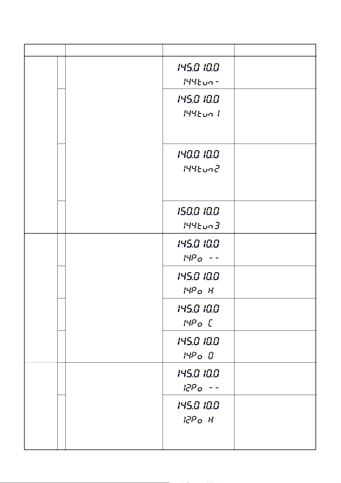
*This output level of a standard signal generator (SSG) is indicated as SSG’s open circuit.
5 - 16
SOFTWARE ADJUSTMENT (continued)
ADJUSTMENT
ITEM (6)
RF PEAK
ADJUSTMENT
ITEM (7)
TX POWER/
METER
(for 144 M)
(for 1200 M)
ADJUSTMENT ADJUSTMENT CONDITION DISPLAY OPERATION
• Enter software adjustment mode (Refer
page 5-12).
• Push [6] key to enter the RF peak adjust-
ment for TX.
• Connect an RF power meter to [VHF ANT]
connector.
• Connect an SSG to P501 on the PA unit
via the JIG cable (A) and set as:
Frequency : 10.850 MHz
Level : 18 mV* (–22 dBm)
Modulation: OFF
NOTE: While transmitting, adjust SSG’s
level and keep the output power less than
30 W.
• Enter software adjustment mode (Refer
page 5-12).
• Push [7] key to enter the TX power/meter
adjustment.
• Connect an RF power meter to [VHF ANT]
connector.
• Connect a digital multimeter or oscillo-
scope to check point CP1631.
1
2
3
4
1
2
3
4
5
6
Push [RIT] key to strat transmitting.
• Pushing [SET] key, tune the [MAIN
DIAL] to maximum.
• Adjust L501, L502 on the PA unit
(illustration for location page 5-9) to
maximum.
• Pushing [SET] key, tune the [MAIN
DIAL] to maximum, then push [RIT]
key to store peak setting into memory and to step next.
(1) Pushing [ATT] key, tune the
[MAIN DIAL] to maximum.
(2) Pushing [SET] key, tune the
[MAIN DIAL] to maximum.
(3) Repeat (1) and (2) several times
until output power will be peak,
then push [RIT] key to store peak
setting into memory and to step
next.
Same as step 3. Then turn power
OFF and ON to return the normal
operation mode. Then continue to
adjust from step 4 of the RF PEAK
adjustment (page 5-8).
Push [RIT] key to strat transmitting.
Tune the [MAIN DIAL] to 100 W
(High power). Push [RIT] key to
store the adjustment value into
memory, and to step next.
Tune the [MAIN DIAL] to 50 W
(Middle power). Push [RIT] key to
store the adjustment value into
memory, and to step next.
Verify the output power (Low power)
is 1–5 W, then push [RIT] key to step
next.
Push [RIT] key to strat transmitting.
Tune the [MAIN DIAL] to 3.0 V at the
check point CP1681. Push [RIT] key
to store the adjustment value into
memory, and to step next.
CWC
W
USBUSB
USBUSB
USBUSB
USBUSB
C
W
CWCWC
W
Page 35
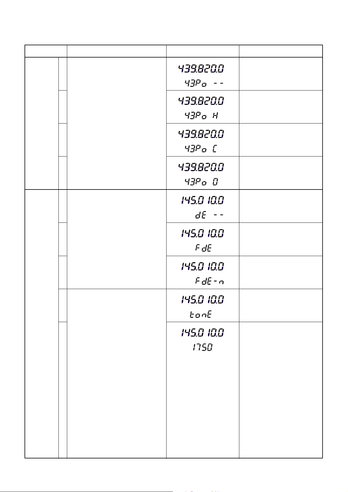
5 - 17
SOFTWARE ADJUSTMENT (continued)
TX POWER/
METER
(for 430 M)
ADJUSTMENT
ITEM (8)
DEVIATION
ADJUSTMENT ADJUSTMENT CONDITION DISPLAY OPERATION
• Connect an RF power meter to [UHF ANT]
connector.
• Enter software adjustment mode (Refer
page 5-12).
• Push [8] key to enter the deviation adjustment.
• MIC gain : Center
• Connect an FM deviation meter to [VHF
ANT] connector through an attenuator and
set as:
HPF : OFF
LPF : 20 kHz
De-emphasis : OFF
Detector : (P–P)/2
• Connect an audio generator to [MIC] connector and set as:
Frequency : 1.0 kHz
Level : 20 mVrms
• Apply no audio signals to [MIC] connector.
7
8
9
10
1
2
3
4
5
Push [RIT] key to strat transmitting.
Tune the [MAIN DIAL] to 75 W (High
power). Push [RIT] key to store the
adjustment value into memory, and
to step next.
Tune the [MAIN DIAL] to 37.5 W
(Middle power). Push [RIT] key to
store the adjustment value into
memory, and to step next.
Verify the output power (Low) is 1–5
W, then push [RIT] key to step next.
Push [RIT] key to strat transmitting.
Tune the [MAIN DIAL] to ±4.5 kHz
FM deviation. Push [RIT] key to
store the adjustment value into
memory, and to step next.
Tune the [MAIN DIAL] to ±2.25 kHz
FM deviation. Push [RIT] key to
store the adjustment value into
memory, and to step next.
Tune the [MAIN DIAL] to ±0.6 kHz
CTCSS tone deviation. Push [RIT]
key to store the adjustment value
into memory, and to step next.
Tune the [MAIN DIAL] to ±0.6 kHz
europe tone deviation. Push [RIT]
key to store the adjustment value
into memory.
Then turn power OFF and ON to
return the normal operation mode.
C
W
CWC
W
C
W
FMFMF
M
N
F
M
T
F
M
T
Page 36

*This output level of a standard signal generator (SSG) is indicated as SSG’s open circuit.
5 - 18
5-7 UX-910 ADJUSTMENTS
2ND LO LOCK
VOLTAGE
1ST LO LOCK
VOLTAGE
RECEIVER
GAIN
ATT GAIN
IDLING
POWER
BALLANCE
TRANSMITTER
GAIN
ADJUSTMENT
ADJUSTMENT ADJUSTMENT CONDITION
MEASUREMENT
VALUE
POINT
UNIT LOCATION UNIT ADJUST
1
1
2
1
1
1
1
2
3
4
1
• Connect an optional UX-910 (1200
MHz band unit).
• Display frequency: 1270.5000 MHz
• Receiving
• Display frequency: 1240.0000 MHz
• Receiving
• Display frequency: 1300.0000 MHz
• Receiving
• Display frequency: 1280.0000 MHz
• Connect a standard signal generator
to [12 ANT] connector and set as:
Frequency : 1280.0000 MHz
Level : 710 µV* (–50 dBm)
Modulation: OFF
• Receiving
• Display frequency: 1280.0000 MHz
• [ATT] : ON
• Set an SSG as :
Frequency : 1280.0000 MHz
Level : 710 µV* (–50 dBm)
Modulation: OFF
• Receiving
• Display frequency: Any
• Mode : CW
• Preset R61, R67, R83 to max.
clockwise, R13 to max. counter
clockwise, and C332 to center.
• Connect an RF power meter to [12
ANT].
• Connect an SSG to the check point
CP311 and set as :
Frequency : 10.8500 MHz
Level : OFF
• Transmitting
• Display frequency: Any
• Mode : CW
• Connect an SSG to the check point
CP311 and set as :
Frequency : 10.8500 MHz
• Transmitting
• Display frequency: 1240.0000 MHz
• Transmitting
• Display frequency: 1300.0000 MHz
• Transmitting
• Display frequency: 1270.0000 MHz
• Set an SSG as :
Frequency : 10.8500 MHz
Level : 18 mV* (–22 dBm)
• Transmitting
MAIN
(UX-910)
MAIN
(UX-910)
MAIN
(UX-910)
MAIN
(UX-910)
MAIN
(UX-910)
Rear
panel
Rear
panel
Connect a digital
multimeter or oscilloscope to check point
CP701.
Connect a digital
multimeter or oscilloscope to check point
CP501.
Connect a spectram
analyzer to check
point CP311.
Connect a spectram
analyzer to check
point CP311.
Connect a digital
multimeter between
check points CP321
and CP322.
Connect an RF
power meter to [12
ANT].
Connect an RF
power meter to [12
ANT].
2.6–3.8 V
6.0–7.0 V
3.4–4.4 V
–34 dBm (16 dB gain)
–14 dBm (20 dB of gain
difference between the
attenuator ON and
OFF.)
0.5 V
voltage difference
5 W
Read the RF power
meter indication.
Same power as step 2
5 W
MAIN
(UX-910)
MAIN
(UX-910)
MAIN
(UX-910)
MAIN
(UX-910)
MAIN
(UX-910)
Verify
Verify
R224
R288
R13
Adjust
SSG’s
level
Verify
C332
R83
Repeat step 2 and step 3 several times until power difference is minimum.
Page 37

5 - 19
CP501
1st LO lock voltage
check point
C332
Power ballance
adjustment
CP322
Idling check point
CP321
Idling check point
R13
Idling adjustment
R67
APC adjustment
R83
Transmitter gain
adjustment
R224
Receiver gain
adjustment
CP15
APC check point
CP701
2nd LO lock voltage
check point
CP311
Receiver gain
check point
CP401
APC check point
R61
APC adjustment
R37
APC adjustment
R288
Attenuator adjustment
Page 38

*This output level of a standard signal generator (SSG) is indicated as SSG’s open circuit.
5 - 20
UX-910 ADJUSTMENTS (continued)
APC
(POWER SET)
ADJUSTMENT
ADJUSTMENT ADJUSTMENT CONDITION
MEASUREMENT
VALUE
POINT
UNIT LOCATION UNIT ADJUST
1
2
3
4
5
• Display frequency: 1270.0000 MHz
• Mode : CW
• Connect an SSG to the check point
CP311 and set as :
Frequency : 10.8500 MHz
• Transmitting
• Transmitting
• Transmitting
• Transmitting
• Transmitting
Rear
panel
MAIN
(UX-910)
Rear
panel
MAIN
(UX-910)
Connect an RF
power meter to [12
ANT].
Connect a digital
multimeter or oscilloscope to check point
CP15.
Connect an RF
power meter to [12
ANT].
Connect a digital
multimeter or oscilloscope to check point
CP401.
Connect a digital
multimeter or oscilloscope to check point
CP15.
13 W
3.0 V
10.5 W
3.1 V
3.0 V
MAIN
(UX-910)
MAIN
(UX-910)
MAIN
(UX-910)
Adjust
SSG’s
level
R37
Adjust
SSG’s
level
R67
R61
Page 39

5 - 21
R67
APC adjustment
CP15
APC check point
CP311
Pre-setting for
APC adjustment
CP401
APC check point
R61
APC adjustment
R37
APC adjustment
Page 40

[DISPLAY BOARD]
6-1 IC-910
[FRONT UNIT]
S.=Surface mount
W1 8900006700 CABLE OPC-645 (N:6 L:60)
W2 8900006700 CABLE OPC-645 (N:6 L:60)
W3 8900006700 CABLE OPC-645 (N:6 L:60)
W4 8900009240 CABLE OPC-909 (P=1 N=10 L=110)
W5 8900006700 CABLE OPC-645 (N:6 L:60)
W6 8900006700 CABLE OPC-645 (N:6 L:60)
EP1 6910012480 E.OTHER RMS20-250-201-1R
EP2 6450001230 E.OTHER HLJ0999-01-480
IC1 1140009671 S.IC M30622MAA-868FP
IC2 1130009970 S.IC SED1540F0A
IC3 1130009100 S.IC BU4052BCFV-E2
IC4 1130009100 S.IC BU4052BCFV-E2
IC5 1130009100 S.IC BU4052BCFV-E2
IC6 1140008650 S.IC HN58X2464TI
IC7 1130009110 S.IC S-80942ANMP-DD6-T2
IC8 1130006800 S.IC TC7W08F (TE12L)
IC9 1130005720 S.IC TC7W04F (TE12L)
IC10 1130007570 S.IC BU4094BCFV-E2
IC11 1180000970 S.IC AN78L05M-(E1)
IC201 1110004200 S.IC NJM2360M-TE3
Q1 1540000550 S.TRANSISTOR 2SD1664 T100Q
Q11 1530002690 S.TRANSISTOR 2SC4116-GR (TE85R)
Q12 1510000770 S.TRANSISTOR 2SA1586-GR (TE85R)
Q13 1530002690 S.TRANSISTOR 2SC4116-GR (TE85R)
Q16 1530002690 S.TRANSISTOR 2SC4116-GR (TE85R)
Q17 1530002690 S.TRANSISTOR 2SC4116-GR (TE85R)
Q18 1590001050 S.TRANSISTOR DTC114TUA T106
Q19 1590001050 S.TRANSISTOR DTC114TUA T106
Q20 1590001050 S.TRANSISTOR DTC114TUA T106
Q21 1590001050 S.TRANSISTOR DTC114TUA T106
Q22 1590000720 S.TRANSISTOR DTA144EUA T106
Q23 1590000720 S.TRANSISTOR DTA144EUA T106
Q24 1520000650 S.TRANSISTOR 2SB1201-S-TL
Q25 1530002690 S.TRANSISTOR 2SC4116-GR (TE85R)
Q26 1590000720 S.TRANSISTOR DTA144EUA T106
D1 1750000550 S.DIODE 1SS355 TE-17 [KOR]
D2 1750000550 S.DIODE 1SS355 TE-17
[USA-1], [AUS], [KOR]
D3 1750000550 S.DIODE 1SS355 TE-17 [EUR]
D5 1750000550 S.DIODE 1SS355 TE-17 except [USA-1]
D6 1750000550 S.DIODE 1SS355 TE-17 except [USA-1]
D7 1750000550 S.DIODE 1SS355 TE-17 except [USA-1]
D9 1750000550 S.DIODE 1SS355 TE-17
D10 1790001610 S.DIODE 1SS385 (TE85L)
D13 1750000550 S.DIODE 1SS355 TE-17
D14 1160000080 S.DIODE DAP202K T146
D15 1750000550 S.DIODE 1SS355 TE-17
D16 1750000550 S.DIODE 1SS355 TE-17
D17 1790001170 S.ZENER MA8068-M (TX)
D20 1750000550 S.DIODE 1SS355 TE-17
D24 1750000550 S.DIODE 1SS355 TE-17
D25 1750000550 S.DIODE 1SS355 TE-17
D26 1750000550 S.DIODE 1SS355 TE-17
D27 1790001670 S.DIODE RB706F-40T106
D28 1790001670 S.DIODE RB706F-40T106
D29 1790001670 S.DIODE RB706F-40T106
D34 1790001670 S.DIODE RB706F-40T106
D35 1790001670 S.DIODE RB706F-40T106
D36 1160000080 S.DIODE DAP202K T146
D37 1750000550 S.DIODE 1SS355 TE-17
D41 1750000550 S.DIODE 1SS355 TE-17
D42 1160000080 S.DIODE DAP202K T146
D43 1160000080 S.DIODE DAP202K T146
D44 1160000080 S.DIODE DAP202K T146
D45 1160000080 S.DIODE DAP202K T146
D46 1160000080 S.DIODE DAP202K T146
D47 1160000080 S.DIODE DAP202K T146
D48 1160000080 S.DIODE DAP202K T146
D49 1160000080 S.DIODE DAP202K T146
D50 1160000080 S.DIODE DAP202K T146
D51 1160000080 S.DIODE DAP202K T146
D52 1160000080 S.DIODE DAP202K T146
D202 1790000670 S.DIODE SB07-03C-TB
X1 6050010500 S.XTAL CR-636 (14.7456 MHz)
L1 6200003950 S.COIL HF50ACC 322513-T
L2 6200003950 S.COIL HF50ACC 322513-T
L3 6200003950 S.COIL HF50ACC 322513-T
L4 6200003950 S.COIL HF50ACC 322513-T
L5 6200003950 S.COIL HF50ACC 322513-T
L6 6200003950 S.COIL HF50ACC 322513-T
L7 6200003950 S.COIL HF50ACC 322513-T
L8 6200003950 S.COIL HF50ACC 322513-T
L10 6200003950 S.COIL HF50ACC 322513-T
L11 6200003330 S.COIL NL 322522T-1R0J-3
L201 6200007030 S.COIL SLF7032T-101MR45-2
L202 6200007030 S.COIL SLF7032T-101MR45-2
L203 6200007030 S.COIL SLF7032T-101MR45-2
R1 7030003440 S.RESISTOR ERJ3GEYJ 102 V (1 kΩ)
R2 7030003640 S.RESISTOR ERJ3GEYJ 473 V (47 kΩ)
R3 7030003640 S.RESISTOR ERJ3GEYJ 473 V (47 kΩ)
R4 7030003640 S.RESISTOR ERJ3GEYJ 473 V (47 kΩ)
R5 7030003640 S.RESISTOR ERJ3GEYJ 473 V (47 kΩ)
R6 7030003640 S.RESISTOR ERJ3GEYJ 473 V (47 kΩ)
R7 7030003640 S.RESISTOR ERJ3GEYJ 473 V (47 kΩ)
R8 7030003640 S.RESISTOR ERJ3GEYJ 473 V (47 kΩ)
R9 7030003640 S.RESISTOR ERJ3GEYJ 473 V (47 kΩ)
R10 7210002230 TRIMMER EVU-FLAEC2 B14
R11 7210002230 TRIMMER EVU-FLAEC2 B14
R12 7030003200 S.RESISTOR ERJ3GEYJ 100 V (10 Ω)
R13 7030003440 S.RESISTOR ERJ3GEYJ 102 V (1 kΩ)
R14 7030003250 S.RESISTOR ERJ3GEYJ 270 V (27 Ω)
R15 7030007990 S.RESISTOR ERJ12YJ820U (82 Ω)
R16 7030007990 S.RESISTOR ERJ12YJ820U (82 Ω)
R17 7030003520 S.RESISTOR ERJ3GEYJ 472 V (4.7 kΩ)
R18 7030003520 S.RESISTOR ERJ3GEYJ 472 V (4.7 kΩ)
R19 7030003680 S.RESISTOR ERJ3GEYJ 104 V (100 kΩ)
R34 7030003560 S.RESISTOR ERJ3GEYJ 103 V (10 kΩ)
R35 7030003560 S.RESISTOR ERJ3GEYJ 103 V (10 kΩ)
R36 7030003680 S.RESISTOR ERJ3GEYJ 104 V (100 kΩ)
R37 7030003630 S.RESISTOR ERJ3GEYJ 393 V (39 kΩ)
R38 7030003560 S.RESISTOR ERJ3GEYJ 103 V (10 kΩ)
R39 7030003640 S.RESISTOR ERJ3GEYJ 473 V (47 kΩ)
R40 7030003680 S.RESISTOR ERJ3GEYJ 104 V (100 kΩ)
R41 7030003360 S.RESISTOR ERJ3GEYJ 221 V (220 Ω)
R42 7030003680 S.RESISTOR ERJ3GEYJ 104 V (100 kΩ)
R43 7030003680 S.RESISTOR ERJ3GEYJ 104 V (100 kΩ)
R44 7030003720 S.RESISTOR ERJ3GEYJ 224 V (220 kΩ)
R45 7030003680 S.RESISTOR ERJ3GEYJ 104 V (100 kΩ)
R46 7030003800 S.RESISTOR ERJ3GEYJ 105 V (1 MΩ)
R47 7030003680 S.RESISTOR ERJ3GEYJ 104 V (100 kΩ)
R48 7030003720 S.RESISTOR ERJ3GEYJ 224 V (220 kΩ)
R49 7030003680 S.RESISTOR ERJ3GEYJ 104 V (100 kΩ)
R50 7030003800 S.RESISTOR ERJ3GEYJ 105 V (1 MΩ)
R51 7030003680 S.RESISTOR ERJ3GEYJ 104 V (100 kΩ)
R52 7030003440 S.RESISTOR ERJ3GEYJ 102 V (1 kΩ)
R53 7030003480 S.RESISTOR ERJ3GEYJ 222 V (2.2 kΩ)
R54 7030003640 S.RESISTOR ERJ3GEYJ 473 V (47 kΩ)
R55 7030003540 S.RESISTOR ERJ3GEYJ 682 V (6.8 kΩ)
R56 7030003620 S.RESISTOR ERJ3GEYJ 333 V (33 kΩ)
6 - 1
SECTION 6 PARTS LIST
REF ORDER
DESCRIPTION
NO. NO.
REF ORDER
DESCRIPTION
NO. NO.
[DISPLAY BOARD]
REF ORDER
DESCRIPTION
NO. NO.
Page 41

[DISPLAY BOARD][DISPLAY BOARD]
S.=Surface mount
R57 7030003640 S.RESISTOR ERJ3GEYJ 473 V (47 kΩ)
R58 7030003590 S.RESISTOR ERJ3GEYJ 183 V (18 kΩ)
R59 7030003680 S.RESISTOR ERJ3GEYJ 104 V (100 kΩ)
R60 7030003480 S.RESISTOR ERJ3GEYJ 222 V (2.2 kΩ)
R61 7030003640 S.RESISTOR ERJ3GEYJ 473 V (47 kΩ)
R66 7030003440 S.RESISTOR ERJ3GEYJ 102 V (1 kΩ)
R67 7030003480 S.RESISTOR ERJ3GEYJ 222 V (2.2 kΩ)
R68 7030003430 S.RESISTOR ERJ3GEYJ 821 V (820 Ω)
R69 7030003640 S.RESISTOR ERJ3GEYJ 473 V (47 kΩ)
R70 7030003640 S.RESISTOR ERJ3GEYJ 473 V (47 kΩ)
R71 7030003440 S.RESISTOR ERJ3GEYJ 102 V (1 kΩ)
R72 7030003480 S.RESISTOR ERJ3GEYJ 222 V (2.2 kΩ)
R73 7030003430 S.RESISTOR ERJ3GEYJ 821 V (820 Ω)
R74 7030000340 S.RESISTOR MCR10EZHJ 470 Ω (471)
R75 7030000330 S.RESISTOR MCR10EZHJ 390 Ω (391)
R76 7030000340 S.RESISTOR MCR10EZHJ 470 Ω (471)
R77 7030000330 S.RESISTOR MCR10EZHJ 390 Ω (391)
R78 7030003840 S.RESISTOR ERJ3GEYJ 225 V (2.2 MΩ)
R79 7030003640 S.RESISTOR ERJ3GEYJ 473 V (47 kΩ)
R80 7030003560 S.RESISTOR ERJ3GEYJ 103 V (10 kΩ)
R81 7030003560 S.RESISTOR ERJ3GEYJ 103 V (10 kΩ)
R82 7030003560 S.RESISTOR ERJ3GEYJ 103 V (10 kΩ)
R83 7030003450 S.RESISTOR ERJ3GEYJ 122 V (1.2 kΩ)
R87 7030000270 S.RESISTOR MCR10EZHJ 120 Ω (121)
R88 7030000270 S.RESISTOR MCR10EZHJ 120 Ω (121)
R90 7030000140 S.RESISTOR MCR10EZHJ 10 Ω (100)
R91 7030003560 S.RESISTOR ERJ3GEYJ 103 V (10 kΩ)
R92 7030003630 S.RESISTOR ERJ3GEYJ 393 V (39 kΩ)
R93 7030003550 S.RESISTOR ERJ3GEYJ 822 V (8.2 kΩ)
R94 7030003570 S.RESISTOR ERJ3GEYJ 123 V (12 kΩ)
R95 7030003400 S.RESISTOR ERJ3GEYJ 471 V (470 Ω)
R96 7030003640 S.RESISTOR ERJ3GEYJ 473 V (47 kΩ)
R97 7030003680 S.RESISTOR ERJ3GEYJ 104 V (100 kΩ)
R98 7030003410 S.RESISTOR ERJ3GEYJ 561 V (560 Ω)
R100 7030003680 S.RESISTOR ERJ3GEYJ 104 V (100 kΩ)
R101 7030003680 S.RESISTOR ERJ3GEYJ 104 V (100 kΩ)
R102 7030003440 S.RESISTOR ERJ3GEYJ 102 V (1 kΩ)
R103 7030003440 S.RESISTOR ERJ3GEYJ 102 V (1 kΩ)
R104 7030003360 S.RESISTOR ERJ3GEYJ 221 V (220 Ω)
R105 7030003360 S.RESISTOR ERJ3GEYJ 221 V (220 Ω)
R106 7030003360 S.RESISTOR ERJ3GEYJ 221 V (220 Ω)
R107 7030003360 S.RESISTOR ERJ3GEYJ 221 V (220 Ω)
R108 7030003360 S.RESISTOR ERJ3GEYJ 221 V (220 Ω)
R109 7030003360 S.RESISTOR ERJ3GEYJ 221 V (220 Ω)
R110 7030003360 S.RESISTOR ERJ3GEYJ 221 V (220 Ω)
R111 7030003680 S.RESISTOR ERJ3GEYJ 104 V (100 kΩ)
R112 7030003680 S.RESISTOR ERJ3GEYJ 104 V (100 kΩ)
R113 7030003360 S.RESISTOR ERJ3GEYJ 221 V (220 Ω)
R114 7030003640 S.RESISTOR ERJ3GEYJ 473 V (47 kΩ)
R115 7030003640 S.RESISTOR ERJ3GEYJ 473 V (47 kΩ)
R116 7030003640 S.RESISTOR ERJ3GEYJ 473 V (47 kΩ)
R117 7030006100 S.RESISTOR RR0816P-183-D (18 kΩ)
R118 7030003560 S.RESISTOR ERJ3GEYJ 103 V (10 kΩ)
R123 7030003360 S.RESISTOR ERJ3GEYJ 221 V (220 Ω)
R124 7030003360 S.RESISTOR ERJ3GEYJ 221 V (220 Ω)
R125 7030003440 S.RESISTOR ERJ3GEYJ 102 V (1 kΩ)
R126 7030003440 S.RESISTOR ERJ3GEYJ 102 V (1 kΩ)
R127 7030003360 S.RESISTOR ERJ3GEYJ 221 V (220 Ω)
R128 7030003360 S.RESISTOR ERJ3GEYJ 221 V (220 Ω)
R129 7030003440 S.RESISTOR ERJ3GEYJ 102 V (1 kΩ)
R130 7030003440 S.RESISTOR ERJ3GEYJ 102 V (1 kΩ)
R131 7030003360 S.RESISTOR ERJ3GEYJ 221 V (220 Ω)
R132 7030003360 S.RESISTOR ERJ3GEYJ 221 V (220 Ω)
R133 7030003360 S.RESISTOR ERJ3GEYJ 221 V (220 Ω)
R134 7030003360 S.RESISTOR ERJ3GEYJ 221 V (220 Ω)
R135 7030003360 S.RESISTOR ERJ3GEYJ 221 V (220 Ω)
R136 7030003360 S.RESISTOR ERJ3GEYJ 221 V (220 Ω)
R137 7030003360 S.RESISTOR ERJ3GEYJ 221 V (220 Ω)
R138 7030003360 S.RESISTOR ERJ3GEYJ 221 V (220 Ω)
R139 7030003800 S.RESISTOR ERJ3GEYJ 105 V (1 MΩ)
R140 7030006100 S.RESISTOR RR0816P-183-D (18 kΩ)
R141 7030003800 S.RESISTOR ERJ3GEYJ 105 V (1 MΩ)
R150 7030006100 S.RESISTOR RR0816P-183-D (18 kΩ)
R151 7030003360 S.RESISTOR ERJ3GEYJ 221 V (220 Ω)
R152 7030003360 S.RESISTOR ERJ3GEYJ 221 V (220 Ω)
R153 7030003360 S.RESISTOR ERJ3GEYJ 221 V (220 Ω)
R154 7030003360 S.RESISTOR ERJ3GEYJ 221 V (220 Ω)
R155 7030003360 S.RESISTOR ERJ3GEYJ 221 V (220 Ω)
R156 7030003360 S.RESISTOR ERJ3GEYJ 221 V (220 Ω)
R157 7030003360 S.RESISTOR ERJ3GEYJ 221 V (220 Ω)
R158 7030004050 S.RESISTOR ERJ3GEYJ 1R0 V (1 Ω)
R159 7030003360 S.RESISTOR ERJ3GEYJ 221 V (220 Ω)
R160 7030003360 S.RESISTOR ERJ3GEYJ 221 V (220 Ω)
R161 7030003360 S.RESISTOR ERJ3GEYJ 221 V (220 Ω)
R162 7030003360 S.RESISTOR ERJ3GEYJ 221 V (220 Ω)
R163 7030003360 S.RESISTOR ERJ3GEYJ 221 V (220 Ω)
R164 7030003360 S.RESISTOR ERJ3GEYJ 221 V (220 Ω)
R165 7030003360 S.RESISTOR ERJ3GEYJ 221 V (220 Ω)
R166 7030003360 S.RESISTOR ERJ3GEYJ 221 V (220 Ω)
R167 7030003360 S.RESISTOR ERJ3GEYJ 221 V (220 Ω)
R168 7030003360 S.RESISTOR ERJ3GEYJ 221 V (220 Ω)
R169 7030003360 S.RESISTOR ERJ3GEYJ 221 V (220 Ω)
R170 7030003360 S.RESISTOR ERJ3GEYJ 221 V (220 Ω)
R171 7030003360 S.RESISTOR ERJ3GEYJ 221 V (220 Ω)
R172 7030003360 S.RESISTOR ERJ3GEYJ 221 V (220 Ω)
R173 7030003680 S.RESISTOR ERJ3GEYJ 104 V (100 kΩ)
R174 7030003680 S.RESISTOR ERJ3GEYJ 104 V (100 kΩ)
R175 7030003680 S.RESISTOR ERJ3GEYJ 104 V (100 kΩ)
R176 7030006100 S.RESISTOR RR0816P-183-D (18 kΩ)
R178 7030003440 S.RESISTOR ERJ3GEYJ 102 V (1 kΩ)
R179 7030003440 S.RESISTOR ERJ3GEYJ 102 V (1 kΩ)
R180 7030003640 S.RESISTOR ERJ3GEYJ 473 V (47 kΩ)
R181 7030003360 S.RESISTOR ERJ3GEYJ 221 V (220 Ω)
R182 7030003360 S.RESISTOR ERJ3GEYJ 221 V (220 Ω)
R183 7030003560 S.RESISTOR ERJ3GEYJ 103 V (10 kΩ)
R184 7030003360 S.RESISTOR ERJ3GEYJ 221 V (220 Ω)
R185 7030003640 S.RESISTOR ERJ3GEYJ 473 V (47 kΩ)
R186 7030003440 S.RESISTOR ERJ3GEYJ 102 V (1 kΩ)
R187 7030003440 S.RESISTOR ERJ3GEYJ 102 V (1 kΩ)
R188 7030003440 S.RESISTOR ERJ3GEYJ 102 V (1 kΩ)
R189 7030003560 S.RESISTOR ERJ3GEYJ 103 V (10 kΩ)
R190 7030003560 S.RESISTOR ERJ3GEYJ 103 V (10 kΩ)]
R201 7030000040 S.RESISTOR MCR10EZHJ 1.5 Ω (1R5)
R202 7030000040 S.RESISTOR MCR10EZHJ 1.5 Ω (1R5)
R203 7030006601 S.RESISTOR ERA3YED 272V
R204 7030006091 S.RESISTOR ERA3YED 822V
R205 7030003680 S.RESISTOR ERJ3GEYJ 104 V (100 kΩ)
C1 4030006860 S.CERAMIC C1608 JB 1H 102K-T-A
C2 4030011600 S.CERAMIC C1608 JB 1C 104KT-N
C3 4030011600 S.CERAMIC C1608 JB 1C 104KT-N
C4 4030011600 S.CERAMIC C1608 JB 1C 104KT-N
C5 4030006860 S.CERAMIC C1608 JB 1H 102K-T-A
C6 4030006860 S.CERAMIC C1608 JB 1H 102K-T-A
C11 4030011600 S.CERAMIC C1608 JB 1C 104KT-N
C12 4030006860 S.CERAMIC C1608 JB 1H 102K-T-A
C13 4030006860 S.CERAMIC C1608 JB 1H 102K-T-A
C14 4030011600 S.CERAMIC C1608 JB 1C 104KT-N
C15 4030008890 S.CERAMIC C1608 JB 1C 273K-T-A
C16 4030006860 S.CERAMIC C1608 JB 1H 102K-T-A
C17 4030007020 S.CERAMIC C1608 CH 1H 120J-T-A
C18 4030007020 S.CERAMIC C1608 CH 1H 120J-T-A
C19 4030006860 S.CERAMIC C1608 JB 1H 102K-T-A
C20 4030007130 S.CERAMIC C1608 CH 1H 101J-T-A
C21 4030011600 S.CERAMIC C1608 JB 1C 104KT-N
C22 4030007130 S.CERAMIC C1608 CH 1H 101J-T-A
C23 4030011600 S.CERAMIC C1608 JB 1C 104KT-N
C24 4030006860 S.CERAMIC C1608 JB 1H 102K-T-A
C25 4030006860 S.CERAMIC C1608 JB 1H 102K-T-A
C27 4030006860 S.CERAMIC C1608 JB 1H 102K-T-A
C29 4030006860 S.CERAMIC C1608 JB 1H 102K-T-A
C30 4030006860 S.CERAMIC C1608 JB 1H 102K-T-A
C31 4030006860 S.CERAMIC C1608 JB 1H 102K-T-A
C32 4030006860 S.CERAMIC C1608 JB 1H 102K-T-A
C33 4030006860 S.CERAMIC C1608 JB 1H 102K-T-A
C34 4030006860 S.CERAMIC C1608 JB 1H 102K-T-A
C36 4030011600 S.CERAMIC C1608 JB 1C 104KT-N
C37 4030011600 S.CERAMIC C1608 JB 1C 104KT-N
C38 4030011600 S.CERAMIC C1608 JB 1C 104KT-N
C39 4030011600 S.CERAMIC C1608 JB 1C 104KT-N
C40 4510006260 S.ELECTROLYTIC ECEV1AA471UP
C41 4030011600 S.CERAMIC C1608 JB 1C 104KT-N
C42 4030011600 S.CERAMIC C1608 JB 1C 104KT-N
C46 4030011600 S.CERAMIC C1608 JB 1C 104KT-N
C47 4510004630 S.ELECTROLYTIC ECEV1CA100SR
C48 4030011600 S.CERAMIC C1608 JB 1C 104KT-N
C49 4030011600 S.CERAMIC C1608 JB 1C 104KT-N
C50 4510004630 S.ELECTROLYTIC ECEV1CA100SR
C51 4510004630 S.ELECTROLYTIC ECEV1CA100SR
C52 4030006860 S.CERAMIC C1608 JB 1H 102K-T-A
C53 4030006860 S.CERAMIC C1608 JB 1H 102K-T-A
C54 4030006860 S.CERAMIC C1608 JB 1H 102K-T-A
C55 4510006220 S.ELECTROLYTIC ECEV1CA101UP
6 - 2
REF ORDER
DESCRIPTION
NO. NO.
REF ORDER
DESCRIPTION
NO. NO.
Page 42

S.=Surface mount
[DISPLAY BOARD][DISPLAY BOARD]
C56 4030006860 S.CERAMIC C1608 JB 1H 102K-T-A
C57 4030012610 S.CERAMIC C2012 JB 1C 474K-T-A
C71 4030006860 S.CERAMIC C1608 JB 1H 102K-T-A
C72 4030006860 S.CERAMIC C1608 JB 1H 102K-T-A
C73 4030006860 S.CERAMIC C1608 JB 1H 102K-T-A
C74 4030006860 S.CERAMIC C1608 JB 1H 102K-T-A
C75 4030006860 S.CERAMIC C1608 JB 1H 102K-T-A
C86 4030012600 S.CERAMIC C2012 JB 1A 105M-T-A
C88 4030006860 S.CERAMIC C1608 JB 1H 102K-T-A
C89 4030006860 S.CERAMIC C1608 JB 1H 102K-T-A
C90 4030006860 S.CERAMIC C1608 JB 1H 102K-T-A
C94 4030011600 S.CERAMIC C1608 JB 1C 104KT-N
C119 4030007130 S.CERAMIC C1608 CH 1H 101J-T-A
C163 4030010760 S.CERAMIC C1608 CH 1H 331J-T-A
C164 4030010760 S.CERAMIC C1608 CH 1H 331J-T-A
C168 4030010760 S.CERAMIC C1608 CH 1H 331J-T-A
C181 4030010760 S.CERAMIC C1608 CH 1H 331J-T-A
C182 4030010760 S.CERAMIC C1608 CH 1H 331J-T-A
C204 4510006220 S.ELECTROLYTIC ECEV1CA101UP
C205 4030011600 S.CERAMIC C1608 JB 1C 104KT-N
C206 4510006220 S.ELECTROLYTIC ECEV1CA101UP
C207 4030011600 S.CERAMIC C1608 JB 1C 104KT-N
C208 4030007150 S.CERAMIC C1608 CH 1H 151J-T-A
C209 4510007580 S.ELECTROLYTIC EEVFC1C101P
C210 4030011600 S.CERAMIC C1608 JB 1C 104KT-N
C211 4030011600 S.CERAMIC C1608 JB 1C 104KT-N
C212 4510006220 S.ELECTROLYTIC ECEV1CA101UP
C213 4030011600 S.CERAMIC C1608 JB 1C 104KT-N
C216 4030011600 S.CERAMIC C1608 JB 1C 104KT-N
C527 4030011600 S.CERAMIC C1608 JB 1C 104KT-N
C536 4030011600 S.CERAMIC C1608 JB 1C 104KT-N
C538 4030011600 S.CERAMIC C1608 JB 1C 104KT-N
C541 4030011600 S.CERAMIC C1608 JB 1C 104KT-N
C542 4030011600 S.CERAMIC C1608 JB 1C 104KT-N
C547 4030011600 S.CERAMIC C1608 JB 1C 104KT-N
C548 4030011600 S.CERAMIC C1608 JB 1C 104KT-N
C549 4030011600 S.CERAMIC C1608 JB 1C 104KT-N
C576 4030011600 S.CERAMIC C1608 JB 1C 104KT-N
C577 4030011600 S.CERAMIC C1608 JB 1C 104KT-N
C600 4030011600 S.CERAMIC C1608 JB 1C 104KT-N
J2 6510022570 S.CONNECTOR 06FMN-BMTTR-A-TBT
J3 6510022570 S.CONNECTOR 06FMN-BMTTR-A-TBT
J4 6510018970 S.CONNECTOR B4B-PH-SM3-TB
J5 6510022570 S.CONNECTOR 06FMN-BMTTR-A-TBT
J6 6510022620 S.CONNECTOR 10FMN-BMTTR-A-TBT
J7 6510021720 S.CONNECTOR 30FLT-SM1-TB
J8 6510021720 S.CONNECTOR 30FLT-SM1-TB
J9 6510022540 S.CONNECTOR 20FMN-BMTTR-A-TBT
J10 6510022290 S.CONNECTOR 06FMN-BMTTR-TBT
J11 6510022290 S.CONNECTOR 06FMN-BMTTR-TBT
J12 6510022190 S.CONNECTOR B3B-PH-SM3-TB
J14 6510018950 S.CONNECTOR B7B-PH-SM3-TB
DS1 5040002680 S.LED TLGE1002
DS2 5040002680 S.LED TLGE1002
DS3 5040002680 S.LED TLGE1002
DS4 5040002680 S.LED TLGE1002
DS5 5040002680 S.LED TLGE1002
DS6 5040002680 S.LED TLGE1002
DS7 5040002680 S.LED TLGE1002
DS8 5040002680 S.LED TLGE1002
DS9 5040002680 S.LED TLGE1002
DS10 5040002680 S.LED TLGE1002
DS11 5040002680 S.LED TLGE1002
DS12 5040002680 S.LED TLGE1002
DS13 5040002680 S.LED TLGE1002
DS14 5040002680 S.LED TLGE1002
DS15 5040002680 S.LED TLGE1002
DS16 5040002680 S.LED TLGE1002
DS17 5040002680 S.LED TLGE1002
DS18 5040002680 S.LED TLGE1002
DS19 5040002680 S.LED TLGE1002
DS20 5040002680 S.LED TLGE1002
DS21 5040002680 S.LED TLGE1002
DS22 5040002680 S.LED TLGE1002
DS23 5040002680 S.LED TLGE1002
DS24 5040002680 S.LED TLGE1002
DS31 5030001840 LCD A0095
DS32 5040001870 S.LED SEC 2462C
DS33 5040001870 S.LED SEC 2462C
W1 7030003860 S.JUMPER ERJ3GE JPW V
W2 7030003860 S.JUMPER ERJ3GE JPW V
EP1 6910012350 S.BEAD MMZ1608Y 102BT
EP2 6910012350 S.BEAD MMZ1608Y 102BT
EP3 6910012350 S.BEAD MMZ1608Y 102BT
EP4 6910012350 S.BEAD MMZ1608Y 102BT
EP5 6910012350 S.BEAD MMZ1608Y 102BT
EP11 0910052635 PCB B 5456E
EP31 8930052490 LCD CONTACT SRCN-2355-SP-N-W
D1 1160000080 S.DIODE DAP202K T146
D2 1160000080 S.DIODE DAP202K T146
D3 1160000080 S.DIODE DAP202K T146
J1 6510022570 S.CONNECTOR 06FMN-BMTTR-A-TBT
EP1 0910052641 PCB B 5458A
R1 7210002970 VARIABLE RV-314 (RK0972210 10KB/10KB)
J1 6510022570 S.CONNECTOR 06FMN-BMTTR-A-TBT
EP1 0910052652 PCB B 5460B
R1 7210002970 VARIABLE RV-314 (RK0972210 10KB/10KB)
J1 6510022570 S.CONNECTOR 06FMN-BMTTR-A-TBT
EP1 0910053410 PCB B 5582
6 - 3
REF ORDER
DESCRIPTION
NO. NO.
REF ORDER
DESCRIPTION
NO. NO.
[FUNC BOARD]
REF ORDER
DESCRIPTION
NO. NO.
[VR-A BOARD]
REF ORDER
DESCRIPTION
NO. NO.
[VR-B BOARD]
REF ORDER
DESCRIPTION
NO. NO.
Page 43

[PLL UNIT][RIT BOARD]
S.=Surface mount
R2 7210003090 VARIABLE
RV-316 (RK0972210C05 10KB/10KB)
J1 6510022570 S.CONNECTOR 06FMN-BMTTR-A-TBT
EP1 0910052661 PCB B 5461A
L1 6200003950 S.COIL HF50ACC 322513-T
R1 7030006070 S.RESISTOR ERJ12YJ101U (100 Ω)
R2 7030006070 S.RESISTOR ERJ12YJ101U (100 Ω)
C1 4030006860 S.CERAMIC C1608 JB 1H 102K-T-A
C2 4030006860 S.CERAMIC C1608 JB 1H 102K-T-A
C3 4030006860 S.CERAMIC C1608 JB 1H 102K-T-A
J1 6450001250 CONNECTOR HLJ4306-01-3070
J2 6510022570 S.CONNECTOR 06FMN-BMTTR-A-TBT
EP1 0910052671 PCB B 5462A
J1 6510000190 CONNECTOR FM214-8SS (P)
J2 6510022620 S.CONNECTOR 10FMN-BMTTR-A-TBT
EP1 0910052682 PCB B 5463B
IC1 1130007700 S.IC BU4094BCF-T1
IC12 1110001900 S.IC µPC4570G2-T1
IC101 1130004830 S.IC TC7SU04F (TE85R)
IC131 1140007880 S.IC TC190G08AF-0046-Z/SC-1246A
IC161 1110001900 S.IC µPC4570G2-T1
IC271 1110004460 S.IC µPB1509GV-E1
IC301 1130004830 S.IC TC7SU04F (TE85R)
IC331 1140007880 S.IC TC190G08AF-0046-Z/SC-1246A
IC471 1110004460 S.IC µPB1509GV-E1
IC501 1180001070 S.IC TA7805F (TE16L)
IC601 1140004550 S.IC M65343FP/SC1287
IC701 1140004550 S.IC M65343FP/SC1287
Q153 1590000660 S.TRANSISTOR DTC144TU T107
Q154 1590000660 S.TRANSISTOR DTC144TU T107
Q161 1590000720 S.TRANSISTOR DTA144EUA T106
Q181 1540000410 S.TRANSISTOR 2SD2345 (TX) S
Q191 1560000650 S.FET 2SK1577-2-T7
Q192 1530003310 S.TRANSISTOR 2SC5107-O (TE85R)
Q261 1530002060 S.TRANSISTOR 2SC4081 T107 R
Q271 1530002060 S.TRANSISTOR 2SC4081 T107 R
Q272 1530003310 S.TRANSISTOR 2SC5107-O (TE85R)
Q361 1590000720 S.TRANSISTOR DTA144EUA T106
Q381 1540000410 S.TRANSISTOR 2SD2345 (TX) S
Q391 1560000650 S.FET 2SK1577-2-T7
Q392 1530003310 S.TRANSISTOR 2SC5107-O (TE85R)
Q471 1530003310 S.TRANSISTOR 2SC5107-O (TE85R)
Q472 1530003310 S.TRANSISTOR 2SC5107-O (TE85R)
Q501 1530002600 S.TRANSISTOR 2SC4215-O (TE85R)
Q541 1530002600 S.TRANSISTOR 2SC4215-O (TE85R)
Q551 1530003310 S.TRANSISTOR 2SC5107-O (TE85R)
Q602 1530002060 S.TRANSISTOR 2SC4081 T107 R
Q702 1530002060 S.TRANSISTOR 2SC4081 T107 R
D161 1750000550 S.DIODE 1SS355 TE-17
D181 1750000550 S.DIODE 1SS355 TE-17
D191 1720000590 S.VARICAP MA357 (TX)
D192 1720000590 S.VARICAP MA357 (TX)
D193 1720000590 S.VARICAP MA357 (TX)
D194 1720000590 S.VARICAP MA357 (TX)
D361 1750000550 S.DIODE 1SS355 TE-17
D381 1750000550 S.DIODE 1SS355 TE-17
D391 1720000590 S.VARICAP MA357 (TX)
D392 1720000590 S.VARICAP MA357 (TX)
D393 1720000590 S.VARICAP MA357 (TX)
D394 1720000590 S.VARICAP MA357 (TX)
X512 6050008710 XTAL CR-452 (30.200 MHz)
L1 6200005010 S.COIL NL 252018T-100J
L101 6200005030 S.COIL NL 252018T-180J
L102 6200005040 S.COIL NL 252018T-220J
L103 6200007020 S.COIL NL 252018T-270J
L131 6200001980 S.COIL NL 252018T-1R0J
L191 6200002040 S.COIL NL 252018T-101J
L193 6130002990 S.COIL LB-345 (5203-T005)
L194 6200003000 S.COIL NL 322522T-R22J-3
L195 6200009350 S.COIL ELJRE R22G-F3
L212 6200005720 S.COIL ELJRE 33NG-F
L213 6200005740 S.COIL ELJRE 47NG-F
L214 6200006990 S.COIL ELJRE 56NG-F
L271 6200005010 S.COIL NL 252018T-100J
L273 6200005740 S.COIL ELJRE 47NG-F
L301 6200005030 S.COIL NL 252018T-180J
L302 6200005040 S.COIL NL 252018T-220J
L303 6200003160 S.COIL NL 322522T-270J
L331 6200009690 S.COIL LQH 4C 101K04
L332 6200008940 S.COIL LQH 3N 331K 34
L391 6200000150 S.COIL NL 322522T-1R0M
L392 6200009260 S.COIL C3328A-5N0J-A
L393 6200009260 S.COIL C3328A-5N0J-A
L394 6200002840 S.COIL NL 252018T-R22J
L395 6200009410 S.COIL C3328A-2N5K-A
L397 6200001980 S.COIL NL 252018T-1R0J
L399 6200005720 S.COIL ELJRE 33NG-F
L421 6200005700 S.COIL ELJRE 22NG-F
L422 6200005700 S.COIL ELJRE 22NG-F
L423 6200005720 S.COIL ELJRE 33NG-F
6 - 4
REF ORDER
DESCRIPTION
NO. NO.
REF ORDER
DESCRIPTION
NO. NO.
[JACK BOARD]
REF ORDER
DESCRIPTION
NO. NO.
[MIC BOARD]
REF ORDER
DESCRIPTION
NO. NO.
Page 44

S.=Surface mount
[PLL UNIT][PLL UNIT]
L424 6200005720 S.COIL ELJRE 33NG-F
L425 6200005700 S.COIL ELJRE 22NG-F
L471 6200005010 S.COIL NL 252018T-100J
L473 6200005720 S.COIL ELJRE 33NG-F
L474 6200001830 S.COIL NL 322522T-100J
L511 6200001830 S.COIL NL 322522T-100J
L541 6200004950 S.COIL NL 252018T-1R8J
L551 6150005090 S.COIL LS-536
L552 6150005090 S.COIL LS-536
L553 6200002180 S.COIL NL 252018T-R12J
L599 6200005010 S.COIL NL 252018T-100J
L601 6200003660 S.COIL NL 252018T-R68J
L602 6200002610 S.COIL NL 252018T-R47J
L604 6200002000 S.COIL NL 252018T-3R3J
L700 6200005010 S.COIL NL 252018T-100J
L701 6200003660 S.COIL NL 252018T-R68J
L702 6200002610 S.COIL NL 252018T-R47J
L704 6200002000 S.COIL NL 252018T-3R3J
R8 7030003360 S.RESISTOR ERJ3GEYJ 221 V (220 Ω)
R9 7030003360 S.RESISTOR ERJ3GEYJ 221 V (220 Ω)
R10 7030003360 S.RESISTOR ERJ3GEYJ 221 V (220 Ω)
R11 7030003360 S.RESISTOR ERJ3GEYJ 221 V (220 Ω)
R12 7030003360 S.RESISTOR ERJ3GEYJ 221 V (220 Ω)
R13 7030003440 S.RESISTOR ERJ3GEYJ 102 V (1 kΩ)
R14 7030003440 S.RESISTOR ERJ3GEYJ 102 V (1 kΩ)
R19 7030003360 S.RESISTOR ERJ3GEYJ 221 V (220 Ω)
R101 7030007230 S.RESISTOR ERA3YED 102V
R102 7030007230 S.RESISTOR ERA3YED 102V
R103 7030007230 S.RESISTOR ERA3YED 102V
R104 7030007230 S.RESISTOR ERA3YED 102V
R105 7030007230 S.RESISTOR ERA3YED 102V
R106 7030007230 S.RESISTOR ERA3YED 102V
R107 7030007210 S.RESISTOR ERA3YEB 102V
R108 7030007210 S.RESISTOR ERA3YEB 102V
R109 7030007210 S.RESISTOR ERA3YEB 102V
R110 7030007210 S.RESISTOR ERA3YEB 102V
R111 7030007210 S.RESISTOR ERA3YEB 102V
R112 7030007220 S.RESISTOR ERA3YED 202V
R113 7030007220 S.RESISTOR ERA3YED 202V
R114 7030007220 S.RESISTOR ERA3YED 202V
R115 7030007220 S.RESISTOR ERA3YED 202V
R116 7030007220 S.RESISTOR ERA3YED 202V
R117 7030007220 S.RESISTOR ERA3YED 202V
R118 7030007220 S.RESISTOR ERA3YED 202V
R119 7030007220 S.RESISTOR ERA3YED 202V
R120 7030007200 S.RESISTOR ERA3YEB 202V
R121 7030007200 S.RESISTOR ERA3YEB 202V
R122 7030007200 S.RESISTOR ERA3YEB 202V
R123 7030007200 S.RESISTOR ERA3YEB 202V
R124 7030007200 S.RESISTOR ERA3YEB 202V
R125 7030003440 S.RESISTOR ERJ3GEYJ 102 V (1 kΩ)
R126 7030003340 S.RESISTOR ERJ3GEYJ 151 V (150 Ω)
R127 7030003800 S.RESISTOR ERJ3GEYJ 105 V (1 MΩ)
R129 7030003320 S.RESISTOR ERJ3GEYJ 101 V (100 Ω)
R130 7030003440 S.RESISTOR ERJ3GEYJ 102 V (1 kΩ)
R131 7030003800 S.RESISTOR ERJ3GEYJ 105 V (1 MΩ)
R132 7030003440 S.RESISTOR ERJ3GEYJ 102 V (1 kΩ)
R133 7030003440 S.RESISTOR ERJ3GEYJ 102 V (1 kΩ)
R134 7030003680 S.RESISTOR ERJ3GEYJ 104 V (100 kΩ)
R135 7030003360 S.RESISTOR ERJ3GEYJ 221 V (220 Ω)
R136 7030003440 S.RESISTOR ERJ3GEYJ 102 V (1 kΩ)
R137 7030003440 S.RESISTOR ERJ3GEYJ 102 V (1 kΩ)
R138 7030003440 S.RESISTOR ERJ3GEYJ 102 V (1 kΩ)
R139 7030003360 S.RESISTOR ERJ3GEYJ 221 V (220 Ω)
R140 7030003360 S.RESISTOR ERJ3GEYJ 221 V (220 Ω)
R160 7030003360 S.RESISTOR ERJ3GEYJ 221 V (220 Ω)
R161 7030004050 S.RESISTOR ERJ3GEYJ 1R0 V (1 Ω)
R162 7030004050 S.RESISTOR ERJ3GEYJ 1R0 V (1 Ω)
R163 7030003320 S.RESISTOR ERJ3GEYJ 101 V (100 Ω)
R164 7030003560 S.RESISTOR ERJ3GEYJ 103 V (10 kΩ)
R165 7030003560 S.RESISTOR ERJ3GEYJ 103 V (10 kΩ)
R166 7030003360 S.RESISTOR ERJ3GEYJ 221 V (220 Ω)
R167 7030003320 S.RESISTOR ERJ3GEYJ 101 V (100 Ω)
R168 7030003360 S.RESISTOR ERJ3GEYJ 221 V (220 Ω)
R169 7030003440 S.RESISTOR ERJ3GEYJ 102 V (1 kΩ)
R170 7030003840 S.RESISTOR ERJ3GEYJ 225 V (2.2 MΩ)
R171 7030003560 S.RESISTOR ERJ3GEYJ 103 V (10 kΩ)
R172 7030003560 S.RESISTOR ERJ3GEYJ 103 V (10 kΩ)
R181 7030003440 S.RESISTOR ERJ3GEYJ 102 V (1 kΩ)
R191 7030003440 S.RESISTOR ERJ3GEYJ 102 V (1 kΩ)
R192 7030003280 S.RESISTOR ERJ3GEYJ 470 V (47 Ω)
R193 7030003440 S.RESISTOR ERJ3GEYJ 102 V (1 kΩ)
R194 7030003620 S.RESISTOR ERJ3GEYJ 333 V (33 kΩ)
R195 7030003360 S.RESISTOR ERJ3GEYJ 221 V (220 Ω)
R211 7030003220 S.RESISTOR ERJ3GEYJ 150 V (15 Ω)
R212 7030003300 S.RESISTOR ERJ3GEYJ 680 V (68 Ω)
R213 7030003220 S.RESISTOR ERJ3GEYJ 150 V (15 Ω)
R252 7030003340 S.RESISTOR ERJ3GEYJ 151 V (150 Ω)
R253 7030003270 S.RESISTOR ERJ3GEYJ 390 V (39 Ω)
R254 7030003340 S.RESISTOR ERJ3GEYJ 151 V (150 Ω)
R261 7030003320 S.RESISTOR ERJ3GEYJ 101 V (100 Ω)
R262 7030003640 S.RESISTOR ERJ3GEYJ 473 V (47 kΩ)
R263 7030003380 S.RESISTOR ERJ3GEYJ 331 V (330 Ω)
R267 7030003440 S.RESISTOR ERJ3GEYJ 102 V (1 kΩ)
R268 7030003350 S.RESISTOR ERJ3GEYJ 181 V (180 Ω)
R271 7030003400 S.RESISTOR ERJ3GEYJ 471 V (470 Ω)
R272 7030003360 S.RESISTOR ERJ3GEYJ 221 V (220 Ω)
R273 7030003640 S.RESISTOR ERJ3GEYJ 473 V (47 kΩ)
R274 7030003360 S.RESISTOR ERJ3GEYJ 221 V (220 Ω)
R275 7030003370 S.RESISTOR ERJ3GEYJ 271 V (270 Ω)
R276 7030003440 S.RESISTOR ERJ3GEYJ 102 V (1 kΩ)
R277 7030003230 S.RESISTOR ERJ3GEYJ 180 V (18 Ω)
R278 7030003370 S.RESISTOR ERJ3GEYJ 271 V (270 Ω)
R281 7030003320 S.RESISTOR ERJ3GEYJ 101 V (100 Ω)
R282 7030003620 S.RESISTOR ERJ3GEYJ 333 V (33 kΩ)
R301 7030007230 S.RESISTOR ERA3YED 102V
R302 7030007230 S.RESISTOR ERA3YED 102V
R303 7030007230 S.RESISTOR ERA3YED 102V
R304 7030007230 S.RESISTOR ERA3YED 102V
R305 7030007230 S.RESISTOR ERA3YED 102V
R306 7030007230 S.RESISTOR ERA3YED 102V
R307 7030007210 S.RESISTOR ERA3YEB 102V
R308 7030007210 S.RESISTOR ERA3YEB 102V
R309 7030007210 S.RESISTOR ERA3YEB 102V
R310 7030007210 S.RESISTOR ERA3YEB 102V
R311 7030007210 S.RESISTOR ERA3YEB 102V
R312 7030007220 S.RESISTOR ERA3YED 202V
R313 7030007220 S.RESISTOR ERA3YED 202V
R314 7030007220 S.RESISTOR ERA3YED 202V
R315 7030007220 S.RESISTOR ERA3YED 202V
R316 7030007220 S.RESISTOR ERA3YED 202V
R317 7030007220 S.RESISTOR ERA3YED 202V
R318 7030007220 S.RESISTOR ERA3YED 202V
R319 7030007220 S.RESISTOR ERA3YED 202V
R320 7030007200 S.RESISTOR ERA3YEB 202V
R321 7030007200 S.RESISTOR ERA3YEB 202V
R322 7030007200 S.RESISTOR ERA3YEB 202V
R323 7030007200 S.RESISTOR ERA3YEB 202V
R324 7030007200 S.RESISTOR ERA3YEB 202V
R325 7030003440 S.RESISTOR ERJ3GEYJ 102 V (1 kΩ)
R326 7030003440 S.RESISTOR ERJ3GEYJ 102 V (1 kΩ)
R327 7030003800 S.RESISTOR ERJ3GEYJ 105 V (1 MΩ)
R330 7030003440 S.RESISTOR ERJ3GEYJ 102 V (1 kΩ)
R331 7030003800 S.RESISTOR ERJ3GEYJ 105 V (1 MΩ)
R332 7030003440 S.RESISTOR ERJ3GEYJ 102 V (1 kΩ)
R333 7030003440 S.RESISTOR ERJ3GEYJ 102 V (1 kΩ)
R334 7030003680 S.RESISTOR ERJ3GEYJ 104 V (100 kΩ)
R335 7030003360 S.RESISTOR ERJ3GEYJ 221 V (220 Ω)
R336 7030003440 S.RESISTOR ERJ3GEYJ 102 V (1 kΩ)
R337 7030003440 S.RESISTOR ERJ3GEYJ 102 V (1 kΩ)
R338 7030003340 S.RESISTOR ERJ3GEYJ 151 V (150 Ω)
R339 7030003360 S.RESISTOR ERJ3GEYJ 221 V (220 Ω)
R340 7030003360 S.RESISTOR ERJ3GEYJ 221 V (220 Ω)
R341 7030003440 S.RESISTOR ERJ3GEYJ 102 V (1 kΩ)
R361 7030003320 S.RESISTOR ERJ3GEYJ 101 V (100 Ω)
R362 7030003550 S.RESISTOR ERJ3GEYJ 822 V (8.2 kΩ)
R363 7030003550 S.RESISTOR ERJ3GEYJ 822 V (8.2 kΩ)
R364 7030003340 S.RESISTOR ERJ3GEYJ 151 V (150 Ω)
R365 7030003340 S.RESISTOR ERJ3GEYJ 151 V (150 Ω)
R366 7030003440 S.RESISTOR ERJ3GEYJ 102 V (1 kΩ)
R367 7030003320 S.RESISTOR ERJ3GEYJ 101 V (100 Ω)
R368 7030003560 S.RESISTOR ERJ3GEYJ 103 V (10 kΩ)
R369 7030003560 S.RESISTOR ERJ3GEYJ 103 V (10 kΩ)
R370 7030003840 S.RESISTOR ERJ3GEYJ 225 V (2.2 MΩ)
R381 7030003400 S.RESISTOR ERJ3GEYJ 471 V (470 Ω)
R391 7030003360 S.RESISTOR ERJ3GEYJ 221 V (220 Ω)
R392 7030003380 S.RESISTOR ERJ3GEYJ 331 V (330 Ω)
R393 7030003440 S.RESISTOR ERJ3GEYJ 102 V (1 kΩ)
R394 7030003620 S.RESISTOR ERJ3GEYJ 333 V (33 kΩ)
R397 7030003340 S.RESISTOR ERJ3GEYJ 151 V (150 Ω)
R425 7030003300 S.RESISTOR ERJ3GEYJ 680 V (68 Ω)
R426 7030003340 S.RESISTOR ERJ3GEYJ 151 V (150 Ω)
6 - 5
REF ORDER
DESCRIPTION
NO. NO.
REF ORDER
DESCRIPTION
NO. NO.
Page 45

[PLL UNIT][PLL UNIT]
S.=Surface mount
R427 7030003300 S.RESISTOR ERJ3GEYJ 680 V (68 Ω)
R474 7030003560 S.RESISTOR ERJ3GEYJ 103 V (10 kΩ)
R475 7030003290 S.RESISTOR ERJ3GEYJ 560 V (56 Ω)
R476 7030003370 S.RESISTOR ERJ3GEYJ 271 V (270 Ω)
R477 7030003230 S.RESISTOR ERJ3GEYJ 180 V (18 Ω)
R478 7030003370 S.RESISTOR ERJ3GEYJ 271 V (270 Ω)
R479 7030003370 S.RESISTOR ERJ3GEYJ 271 V (270 Ω)
R481 7030003320 S.RESISTOR ERJ3GEYJ 101 V (100 Ω)
R482 7030003620 S.RESISTOR ERJ3GEYJ 333 V (33 kΩ)
R483 7030003440 S.RESISTOR ERJ3GEYJ 102 V (1 kΩ)
R501 7030008190 S.RESISTOR ERJ12YJ330U (33 Ω)
R502 7030008190 S.RESISTOR ERJ12YJ330U (33 Ω)
R503 7030008190 S.RESISTOR ERJ12YJ330U (33 Ω)
R515 7030003420 S.RESISTOR ERJ3GEYJ 681 V (680 Ω)
R538 7030003470 S.RESISTOR ERJ3GEYJ 182 V (1.8 kΩ)
R541 7030003420 S.RESISTOR ERJ3GEYJ 681 V (680 Ω)
R542 7030003630 S.RESISTOR ERJ3GEYJ 393 V (39 kΩ)
R543 7030003320 S.RESISTOR ERJ3GEYJ 101 V (100 Ω)
R544 7030003400 S.RESISTOR ERJ3GEYJ 471 V (470 Ω)
R545 7030003270 S.RESISTOR ERJ3GEYJ 390 V (39 Ω)
R547 7030003330 S.RESISTOR ERJ3GEYJ 121 V (120 Ω)
R548 7030003330 S.RESISTOR ERJ3GEYJ 121 V (120 Ω)
R551 7030003460 S.RESISTOR ERJ3GEYJ 152 V (1.5 kΩ)
R552 7030003320 S.RESISTOR ERJ3GEYJ 101 V (100 Ω)
R553 7030003580 S.RESISTOR ERJ3GEYJ 153 V (15 kΩ)
R554 7030003530 S.RESISTOR ERJ3GEYJ 562 V (5.6 kΩ)
R555 7030003340 S.RESISTOR ERJ3GEYJ 151 V (150 Ω)
R556 7030003320 S.RESISTOR ERJ3GEYJ 101 V (100 Ω)
R557 7030003290 S.RESISTOR ERJ3GEYJ 560 V (56 Ω)
R558 7030003320 S.RESISTOR ERJ3GEYJ 101 V (100 Ω)
R559 7510001190 S.THERMISTOR NTCCM1608 4BH 472KC
R568 7030003640 S.RESISTOR ERJ3GEYJ 473 V (47 kΩ)
R569 7030003320 S.RESISTOR ERJ3GEYJ 101 V (100 Ω)
R570 7310002720 S.TRIMMER RV-148 (RH03A3AS3X0DA) 472
R571 7030003360 S.RESISTOR ERJ3GEYJ 221 V (220 Ω)
R572 7030003600 S.RESISTOR ERJ3GEYJ 223 V (22 kΩ)
R601 7030007230 S.RESISTOR ERA3YED 102V
R602 7030007230 S.RESISTOR ERA3YED 102V
R603 7030007230 S.RESISTOR ERA3YED 102V
R604 7030007230 S.RESISTOR ERA3YED 102V
R605 7030007230 S.RESISTOR ERA3YED 102V
R606 7030007230 S.RESISTOR ERA3YED 102V
R607 7030007210 S.RESISTOR ERA3YEB 102V
R608 7030007210 S.RESISTOR ERA3YEB 102V
R609 7030007210 S.RESISTOR ERA3YEB 102V
R610 7030007220 S.RESISTOR ERA3YED 202V
R611 7030007220 S.RESISTOR ERA3YED 202V
R612 7030007220 S.RESISTOR ERA3YED 202V
R613 7030007220 S.RESISTOR ERA3YED 202V
R614 7030007220 S.RESISTOR ERA3YED 202V
R615 7030007220 S.RESISTOR ERA3YED 202V
R616 7030007220 S.RESISTOR ERA3YED 202V
R617 7030007200 S.RESISTOR ERA3YEB 202V
R618 7030007200 S.RESISTOR ERA3YEB 202V
R619 7030007200 S.RESISTOR ERA3YEB 202V
R620 7030007200 S.RESISTOR ERA3YEB 202V
R621 7030003350 S.RESISTOR ERJ3GEYJ 181 V (180 Ω)
R622 7030003360 S.RESISTOR ERJ3GEYJ 221 V (220 Ω)
R623 7030003640 S.RESISTOR ERJ3GEYJ 473 V (47 kΩ)
R625 7030003370 S.RESISTOR ERJ3GEYJ 271 V (270 Ω)
R626 7030003230 S.RESISTOR ERJ3GEYJ 180 V (18 Ω)
R627 7030003370 S.RESISTOR ERJ3GEYJ 271 V (270 Ω)
R628 7030003440 S.RESISTOR ERJ3GEYJ 102 V (1 kΩ)
R629 7030003360 S.RESISTOR ERJ3GEYJ 221 V (220 Ω)
R630 7030003360 S.RESISTOR ERJ3GEYJ 221 V (220 Ω)
R631 7030003360 S.RESISTOR ERJ3GEYJ 221 V (220 Ω)
R701 7030007230 S.RESISTOR ERA3YED 102V
R702 7030007230 S.RESISTOR ERA3YED 102V
R703 7030007230 S.RESISTOR ERA3YED 102V
R704 7030007230 S.RESISTOR ERA3YED 102V
R705 7030007230 S.RESISTOR ERA3YED 102V
R706 7030007230 S.RESISTOR ERA3YED 102V
R707 7030007210 S.RESISTOR ERA3YEB 102V
R708 7030007210 S.RESISTOR ERA3YEB 102V
R709 7030007210 S.RESISTOR ERA3YEB 102V
R710 7030007220 S.RESISTOR ERA3YED 202V
R711 7030007220 S.RESISTOR ERA3YED 202V
R712 7030007220 S.RESISTOR ERA3YED 202V
R713 7030007220 S.RESISTOR ERA3YED 202V
R714 7030007220 S.RESISTOR ERA3YED 202V
R715 7030007220 S.RESISTOR ERA3YED 202V
R716 7030007220 S.RESISTOR ERA3YED 202V
R717 7030007200 S.RESISTOR ERA3YEB 202V
R718 7030007200 S.RESISTOR ERA3YEB 202V
R719 7030007200 S.RESISTOR ERA3YEB 202V
R720 7030007200 S.RESISTOR ERA3YEB 202V
R721 7030003350 S.RESISTOR ERJ3GEYJ 181 V (180 Ω)
R722 7030003360 S.RESISTOR ERJ3GEYJ 221 V (220 Ω)
R723 7030003640 S.RESISTOR ERJ3GEYJ 473 V (47 kΩ)
R725 7030003370 S.RESISTOR ERJ3GEYJ 271 V (270 Ω)
R726 7030003230 S.RESISTOR ERJ3GEYJ 180 V (18 Ω)
R727 7030003370 S.RESISTOR ERJ3GEYJ 271 V (270 Ω)
R728 7030003440 S.RESISTOR ERJ3GEYJ 102 V (1 kΩ)
R729 7030003360 S.RESISTOR ERJ3GEYJ 221 V (220 Ω)
R730 7030003360 S.RESISTOR ERJ3GEYJ 221 V (220 Ω)
R731 7030003360 S.RESISTOR ERJ3GEYJ 221 V (220 Ω)
C1 4030006900 S.CERAMIC C1608 JB 1E 103K-T-A
C2 4030006860 S.CERAMIC C1608 JB 1H 102K-T-A
C3 4030006860 S.CERAMIC C1608 JB 1H 102K-T-A
C4 4030006860 S.CERAMIC C1608 JB 1H 102K-T-A
C5 4030006860 S.CERAMIC C1608 JB 1H 102K-T-A
C9 4030006860 S.CERAMIC C1608 JB 1H 102K-T-A
C12 4030006860 S.CERAMIC C1608 JB 1H 102K-T-A
C13 4030006860 S.CERAMIC C1608 JB 1H 102K-T-A
C14 4030006860 S.CERAMIC C1608 JB 1H 102K-T-A
C15 4030011600 S.CERAMIC C1608 JB 1C 104KT-N
C16 4030011600 S.CERAMIC C1608 JB 1C 104KT-N
C101 4030007010 S.CERAMIC C1608 CH 1H 100D-T-A
C102 4030007010 S.CERAMIC C1608 CH 1H 100D-T-A
C103 4030007080 S.CERAMIC C1608 CH 1H 390J-T-A
C104 4030007050 S.CERAMIC C1608 CH 1H 220J-T-A
C105 4030007100 S.CERAMIC C1608 CH 1H 560J-T-A
C106 4030007020 S.CERAMIC C1608 CH 1H 120J-T-A
C107 4030007110 S.CERAMIC C1608 CH 1H 680J-T-A
C108 4030006950 S.CERAMIC C1608 CH 1H 040C-T-A
C109 4030007100 S.CERAMIC C1608 CH 1H 560J-T-A
C110 4030007060 S.CERAMIC C1608 CH 1H 270J-T-A
C111 4030008920 S.CERAMIC C1608 JB 1C 473K-T-A
C113 4030008920 S.CERAMIC C1608 JB 1C 473K-T-A
C121 4030008920 S.CERAMIC C1608 JB 1C 473K-T-A
C122 4030012600 S.CERAMIC C2012 JB 1A 105M-T-A
C123 4030007110 S.CERAMIC C1608 CH 1H 680J-T-A
C124 4030007040 S.CERAMIC C1608 CH 1H 180J-T-A
C131 4030008920 S.CERAMIC C1608 JB 1C 473K-T-A
C132 4030008920 S.CERAMIC C1608 JB 1C 473K-T-A
C133 4030008920 S.CERAMIC C1608 JB 1C 473K-T-A
C134 4030008920 S.CERAMIC C1608 JB 1C 473K-T-A
C135 4030008920 S.CERAMIC C1608 JB 1C 473K-T-A
C136 4030008920 S.CERAMIC C1608 JB 1C 473K-T-A
C137 4030007110 S.CERAMIC C1608 CH 1H 680J-T-A
C138 4030008920 S.CERAMIC C1608 JB 1C 473K-T-A
C139 4030008920 S.CERAMIC C1608 JB 1C 473K-T-A
C140 4030007130 S.CERAMIC C1608 CH 1H 101J-T-A
C141 4030008920 S.CERAMIC C1608 JB 1C 473K-T-A
C142 4030008920 S.CERAMIC C1608 JB 1C 473K-T-A
C143 4030008920 S.CERAMIC C1608 JB 1C 473K-T-A
C144 4030008920 S.CERAMIC C1608 JB 1C 473K-T-A
C145 4030008920 S.CERAMIC C1608 JB 1C 473K-T-A
C146 4030008920 S.CERAMIC C1608 JB 1C 473K-T-A
C147 4550006700 S.TANTALUM ECST1AY106R
C148 4030006860 S.CERAMIC C1608 JB 1H 102K-T-A
C153 4030006900 S.CERAMIC C1608 JB 1E 103K-T-A
C161 4030006860 S.CERAMIC C1608 JB 1H 102K-T-A
C162 4030006850 S.CERAMIC C1608 JB 1H 471K-T-A
C163 4510004630 S.ELECTROLYTIC ECEV1CA100SR
C164 4550006170 S.TANTALUM ECST1AY225R
C165 4550006170 S.TANTALUM ECST1AY225R
C166 4550006150 S.TANTALUM ECST1CY105R
C167 4030006860 S.CERAMIC C1608 JB 1H 102K-T-A
C168 4030006850 S.CERAMIC C1608 JB 1H 471K-T-A
C169 4510004630 S.ELECTROLYTIC ECEV1CA100SR
C170 4030006860 S.CERAMIC C1608 JB 1H 102K-T-A
C171 4030008920 S.CERAMIC C1608 JB 1C 473K-T-A
C172 4030006860 S.CERAMIC C1608 JB 1H 102K-T-A
C173 4030006860 S.CERAMIC C1608 JB 1H 102K-T-A
C174 4030006860 S.CERAMIC C1608 JB 1H 102K-T-A
C175 4510004440 S.ELECTROLYTIC ECEV1HA010SR
C181 4510004630 S.ELECTROLYTIC ECEV1CA100SR
C182 4510004630 S.ELECTROLYTIC ECEV1CA100SR
C183 4030006860 S.CERAMIC C1608 JB 1H 102K-T-A
C184 4030006860 S.CERAMIC C1608 JB 1H 102K-T-A
C191 4030007070 S.CERAMIC C1608 CH 1H 330J-T-A
6 - 6
REF ORDER
DESCRIPTION
NO. NO.
REF ORDER
DESCRIPTION
NO. NO.
Page 46

S.=Surface mount
[PLL UNIT][PLL UNIT]
C192 4030006860 S.CERAMIC C1608 JB 1H 102K-T-A
C193 4030006860 S.CERAMIC C1608 JB 1H 102K-T-A
C194 4030006910 S.CERAMIC C1608 CH 1H 0R5C-T-A
C196 4030006860 S.CERAMIC C1608 JB 1H 102K-T-A
C198 4030007090 S.CERAMIC C1608 CH 1H 470J-T-A
C213 4030007060 S.CERAMIC C1608 CH 1H 270J-T-A
C214 4030009920 S.CERAMIC C1608 CH 1H 050B-T-A
C215 4030007070 S.CERAMIC C1608 CH 1H 330J-T-A
C216 4030009520 S.CERAMIC C1608 CH 1H 020B-T-A
C217 4030007040 S.CERAMIC C1608 CH 1H 180J-T-A
C229 4030006860 S.CERAMIC C1608 JB 1H 102K-T-A
C251 4030006860 S.CERAMIC C1608 JB 1H 102K-T-A
C253 4030007010 S.CERAMIC C1608 CH 1H 100D-T-A
C254 4030007010 S.CERAMIC C1608 CH 1H 100D-T-A
C261 4030006880 S.CERAMIC C1608 JB 1H 472K-T-A
C262 4030006880 S.CERAMIC C1608 JB 1H 472K-T-A
C263 4030006880 S.CERAMIC C1608 JB 1H 472K-T-A
C273 4030006860 S.CERAMIC C1608 JB 1H 102K-T-A
C274 4030011600 S.CERAMIC C1608 JB 1C 104KT-N
C275 4030006880 S.CERAMIC C1608 JB 1H 472K-T-A
C276 4030006860 S.CERAMIC C1608 JB 1H 102K-T-A
C277 4030006980 S.CERAMIC C1608 CH 1H 070D-T-A
C278 4030006860 S.CERAMIC C1608 JB 1H 102K-T-A
C279 4030006860 S.CERAMIC C1608 JB 1H 102K-T-A
C280 4030006860 S.CERAMIC C1608 JB 1H 102K-T-A
C281 4030007010 S.CERAMIC C1608 CH 1H 100D-T-A
C283 4030006860 S.CERAMIC C1608 JB 1H 102K-T-A
C284 4030007050 S.CERAMIC C1608 CH 1H 220J-T-A
C301 4030007010 S.CERAMIC C1608 CH 1H 100D-T-A
C302 4030007010 S.CERAMIC C1608 CH 1H 100D-T-A
C303 4030007010 S.CERAMIC C1608 CH 1H 100D-T-A
C304 4030007090 S.CERAMIC C1608 CH 1H 470J-T-A
C306 4030007120 S.CERAMIC C1608 CH 1H 820J-T-A
C308 4030007110 S.CERAMIC C1608 CH 1H 680J-T-A
C310 4030007100 S.CERAMIC C1608 CH 1H 560J-T-A
C312 4030008920 S.CERAMIC C1608 JB 1C 473K-T-A
C314 4030008920 S.CERAMIC C1608 JB 1C 473K-T-A
C321 4030008920 S.CERAMIC C1608 JB 1C 473K-T-A
C322 4030012600 S.CERAMIC C2012 JB 1A 105M-T-A
C323 4030007050 S.CERAMIC C1608 CH 1H 220J-T-A
C325 4030007020 S.CERAMIC C1608 CH 1H 120J-T-A
C327 4550006670 S.TANTALUM ECST1AD107R
C329 4550006670 S.TANTALUM ECST1AD107R
C330 4030007090 S.CERAMIC C1608 CH 1H 470J-T-A
C331 4030008920 S.CERAMIC C1608 JB 1C 473K-T-A
C332 4030008920 S.CERAMIC C1608 JB 1C 473K-T-A
C333 4030008920 S.CERAMIC C1608 JB 1C 473K-T-A
C334 4030008920 S.CERAMIC C1608 JB 1C 473K-T-A
C335 4030008920 S.CERAMIC C1608 JB 1C 473K-T-A
C336 4030008920 S.CERAMIC C1608 JB 1C 473K-T-A
C337 4030008920 S.CERAMIC C1608 JB 1C 473K-T-A
C339 4030008920 S.CERAMIC C1608 JB 1C 473K-T-A
C340 4030008920 S.CERAMIC C1608 JB 1C 473K-T-A
C341 4030008920 S.CERAMIC C1608 JB 1C 473K-T-A
C342 4030008920 S.CERAMIC C1608 JB 1C 473K-T-A
C343 4030008920 S.CERAMIC C1608 JB 1C 473K-T-A
C344 4030008920 S.CERAMIC C1608 JB 1C 473K-T-A
C345 4030008920 S.CERAMIC C1608 JB 1C 473K-T-A
C347 4550006700 S.TANTALUM ECST1AY106R
C348 4030006860 S.CERAMIC C1608 JB 1H 102K-T-A
C350 4030006900 S.CERAMIC C1608 JB 1E 103K-T-A
C362 4550006170 S.TANTALUM ECST1AY225R
C363 4550006170 S.TANTALUM ECST1AY225R
C364 4510004630 S.ELECTROLYTIC ECEV1CA100SR
C365 4030006850 S.CERAMIC C1608 JB 1H 471K-T-A
C366 4030006860 S.CERAMIC C1608 JB 1H 102K-T-A
C368 4550006150 S.TANTALUM ECST1CY105R
C369 4510004630 S.ELECTROLYTIC ECEV1CA100SR
C370 4030006850 S.CERAMIC C1608 JB 1H 471K-T-A
C371 4030006860 S.CERAMIC C1608 JB 1H 102K-T-A
C372 4030007130 S.CERAMIC C1608 CH 1H 101J-T-A
C373 4030006850 S.CERAMIC C1608 JB 1H 471K-T-A
C374 4030006850 S.CERAMIC C1608 JB 1H 471K-T-A
C375 4030006860 S.CERAMIC C1608 JB 1H 102K-T-A
C376 4030006860 S.CERAMIC C1608 JB 1H 102K-T-A
C377 4510004440 S.ELECTROLYTIC ECEV1HA010SR
C381 4510005370 S.ELECTROLYTIC ECEV1AA221P
C382 4030006860 S.CERAMIC C1608 JB 1H 102K-T-A
C383 4030006860 S.CERAMIC C1608 JB 1H 102K-T-A
C391 4030006850 S.CERAMIC C1608 JB 1H 471K-T-A
C392 4030008920 S.CERAMIC C1608 JB 1C 473K-T-A
C393 4030006860 S.CERAMIC C1608 JB 1H 102K-T-A
C394 4030006850 S.CERAMIC C1608 JB 1H 471K-T-A
C398 4030006860 S.CERAMIC C1608 JB 1H 102K-T-A
C399 4030006860 S.CERAMIC C1608 JB 1H 102K-T-A
C401 4030011340 S.CERAMIC C1608 CH 1H 471J-T-A
C402 4610001920 S.TRIMMER TZC03Z060A110 6P
C403 4030006950 S.CERAMIC C1608 CH 1H 040C-T-A
C404 4030006950 S.CERAMIC C1608 CH 1H 040C-T-A
C405 4030009500 S.CERAMIC C1608 CH 1H 0R5B-T-A
C407 4030006860 S.CERAMIC C1608 JB 1H 102K-T-A
C408 4030006860 S.CERAMIC C1608 JB 1H 102K-T-A
C410 4030011340 S.CERAMIC C1608 CH 1H 471J-T-A
C413 4030006960 S.CERAMIC C1608 CH 1H 050C-T-A
C421 4030006980 S.CERAMIC C1608 CH 1H 070D-T-A
C422 4030006930 S.CERAMIC C1608 CH 1H 020C-T-A
C423 4030006980 S.CERAMIC C1608 CH 1H 070D-T-A
C426 4030006960 S.CERAMIC C1608 CH 1H 050C-T-A
C428 4030006980 S.CERAMIC C1608 CH 1H 070D-T-A
C430 4030006960 S.CERAMIC C1608 CH 1H 050C-T-A
C471 4030008920 S.CERAMIC C1608 JB 1C 473K-T-A
C472 4030012600 S.CERAMIC C2012 JB 1A 105M-T-A
C474 4030007090 S.CERAMIC C1608 CH 1H 470J-T-A
C475 4030006860 S.CERAMIC C1608 JB 1H 102K-T-A
C476 4030006860 S.CERAMIC C1608 JB 1H 102K-T-A
C478 4030011600 S.CERAMIC C1608 JB 1C 104KT-N
C480 4030006860 S.CERAMIC C1608 JB 1H 102K-T-A
C481 4030006860 S.CERAMIC C1608 JB 1H 102K-T-A
C482 4030006860 S.CERAMIC C1608 JB 1H 102K-T-A
C483 4030006860 S.CERAMIC C1608 JB 1H 102K-T-A
C484 4030006860 S.CERAMIC C1608 JB 1H 102K-T-A
C485 4030006920 S.CERAMIC C1608 CH 1H 010C-T-A
C487 4030006860 S.CERAMIC C1608 JB 1H 102K-T-A
C488 4030006860 S.CERAMIC C1608 JB 1H 102K-T-A
C501 4030008920 S.CERAMIC C1608 JB 1C 473K-T-A
C502 4510004630 S.ELECTROLYTIC ECEV1CA100SR
C503 4510004630 S.ELECTROLYTIC ECEV1CA100SR
C504 4030008920 S.CERAMIC C1608 JB 1C 473K-T-A
C505 4030006860 S.CERAMIC C1608 JB 1H 102K-T-A
C511 4030006880 S.CERAMIC C1608 JB 1H 472K-T-A
C512 4510006220 S.ELECTROLYTIC ECEV1CA101UP
C513 4030006860 S.CERAMIC C1608 JB 1H 102K-T-A
C514 4030006880 S.CERAMIC C1608 JB 1H 472K-T-A
C515 4030006980 S.CERAMIC C1608 CH 1H 070D-T-A
C535 4030006880 S.CERAMIC C1608 JB 1H 472K-T-A
C541 4030006860 S.CERAMIC C1608 JB 1H 102K-T-A
C542 4030006860 S.CERAMIC C1608 JB 1H 102K-T-A
C543 4030006880 S.CERAMIC C1608 JB 1H 472K-T-A
C544 4030007030 S.CERAMIC C1608 CH 1H 150J-T-A
C545 4030006860 S.CERAMIC C1608 JB 1H 102K-T-A
C551 4030006860 S.CERAMIC C1608 JB 1H 102K-T-A
C552 4030006880 S.CERAMIC C1608 JB 1H 472K-T-A
C553 4030006860 S.CERAMIC C1608 JB 1H 102K-T-A
C554 4030007050 S.CERAMIC C1608 CH 1H 220J-T-A
C555 4030006880 S.CERAMIC C1608 JB 1H 472K-T-A
C556 4030006920 S.CERAMIC C1608 CH 1H 010C-T-A
C557 4030007050 S.CERAMIC C1608 CH 1H 220J-T-A
C558 4030006860 S.CERAMIC C1608 JB 1H 102K-T-A
C559 4030007110 S.CERAMIC C1608 CH 1H 680J-T-A
C560 4030007110 S.CERAMIC C1608 CH 1H 680J-T-A
C574 4030006880 S.CERAMIC C1608 JB 1H 472K-T-A
C575 4030011600 S.CERAMIC C1608 JB 1C 104KT-N
C601 4030007170 S.CERAMIC C1608 CH 1H 221J-T-A
C602 4030007100 S.CERAMIC C1608 CH 1H 560J-T-A
C603 4030011330 S.CERAMIC C1608 CH 1H 391J-T-A
C604 4030007160 S.CERAMIC C1608 CH 1H 181J-T-A
C605 4030007160 S.CERAMIC C1608 CH 1H 181J-T-A
C608 4030007110 S.CERAMIC C1608 CH 1H 680J-T-A
C609 4030006900 S.CERAMIC C1608 JB 1E 103K-T-A
C610 4030006900 S.CERAMIC C1608 JB 1E 103K-T-A
C611 4030006900 S.CERAMIC C1608 JB 1E 103K-T-A
C613 4030006880 S.CERAMIC C1608 JB 1H 472K-T-A
C614 4030006900 S.CERAMIC C1608 JB 1E 103K-T-A
C615 4030006900 S.CERAMIC C1608 JB 1E 103K-T-A
C616 4030006900 S.CERAMIC C1608 JB 1E 103K-T-A
C617 4030006900 S.CERAMIC C1608 JB 1E 103K-T-A
C618 4030011600 S.CERAMIC C1608 JB 1C 104KT-N
C619 4550006700 S.TANTALUM ECST1AY106R
C620 4030007130 S.CERAMIC C1608 CH 1H 101J-T-A
C621 4030007130 S.CERAMIC C1608 CH 1H 101J-T-A
C701 4030007170 S.CERAMIC C1608 CH 1H 221J-T-A
C702 4030007100 S.CERAMIC C1608 CH 1H 560J-T-A
C703 4030011330 S.CERAMIC C1608 CH 1H 391J-T-A
C704 4030007160 S.CERAMIC C1608 CH 1H 181J-T-A
6 - 7
REF ORDER
DESCRIPTION
NO. NO.
REF ORDER
DESCRIPTION
NO. NO.
Page 47

[MAIN UNIT][PLL UNIT]
S.=Surface mount
C705 4030007160 S.CERAMIC C1608 CH 1H 181J-T-A
C708 4030007110 S.CERAMIC C1608 CH 1H 680J-T-A
C709 4030006900 S.CERAMIC C1608 JB 1E 103K-T-A
C710 4030006900 S.CERAMIC C1608 JB 1E 103K-T-A
C711 4030006900 S.CERAMIC C1608 JB 1E 103K-T-A
C713 4030006880 S.CERAMIC C1608 JB 1H 472K-T-A
C714 4030006900 S.CERAMIC C1608 JB 1E 103K-T-A
C715 4030006900 S.CERAMIC C1608 JB 1E 103K-T-A
C716 4030006900 S.CERAMIC C1608 JB 1E 103K-T-A
C717 4030006900 S.CERAMIC C1608 JB 1E 103K-T-A
C718 4030011600 S.CERAMIC C1608 JB 1C 104KT-N
C719 4550006700 S.TANTALUM ECST1AY106R
C720 4030007130 S.CERAMIC C1608 CH 1H 101J-T-A
C721 4030007130 S.CERAMIC C1608 CH 1H 101J-T-A
J1 6510022540 S.CONNECTOR 20FMN-BMTTR-A-TBT
J541 6510007020 CONNECTOR TMP-J01X-V6
W603 7030003860 S.JUMPER ERJ3GE JPW V
W703 7030003860 S.JUMPER ERJ3GE JPW V
WS1 8970023740 E.OTHER
SX2355 1.5D COAXIAL TUBE (1)/PL
WS2 8970023750 E.OTHER
SX2355 1.5D COAXIAL TUBE (1)/PL
WS3 8970023760 E.OTHER
SX2355 0.8D COAXIAL TUBE (1)/PL
WS4 8970023770 E.OTHER
SX2355 0.8D COAXIAL TUBE (2)/PL
EP1 0910052695 PCB B 5464E
IC101 1110003140 IC LA1150N
IC201 1110004840 S.IC NJM1496V-TE1
IC351 1110004870 S.IC TA4101F (TE12L)
IC401 1110003490 S.IC TA31136FN (D,EL)
IC451 1110003870 S.IC NJM2058M-T1
IC452 1130008230 S.IC BU4053BCFV-E2
IC701 1110003140 IC LA1150N
IC801 1180002040 REG BA09T
IC803 1110002020 IC TA7805S
IC851 1110004870 S.IC TA4101F (TE12L)
IC951 1110003490 S.IC TA31136FN (D,EL)
IC1001 1110003870 S.IC NJM2058M-T1
IC1002 1130008230 S.IC BU4053BCFV-E2
IC1101 1130007040 S.IC TC7W32F (TE12L)
IC1451 1130007570 S.IC BU4094BCFV-E2
IC1461 1130007570 S.IC BU4094BCFV-E2
IC1471 1130007570 S.IC BU4094BCFV-E2
IC1481 1130007570 S.IC BU4094BCFV-E2
IC1491 1130007570 S.IC BU4094BCFV-E2
IC1511 1130007570 S.IC BU4094BCFV-E2
IC1521 1110004310 S.IC M62352GP 75EC
IC1522 1110003870 S.IC NJM2058M-T1
IC1531 1130008230 S.IC BU4053BCFV-E2
IC1551 1130008230 S.IC BU4053BCFV-E2
IC1552 1130008230 S.IC BU4053BCFV-E2
IC1601 1110003870 S.IC NJM2058M-T1
IC1651 1110005240 S.IC NJM4565M-T1
IC1652 1110003870 S.IC NJM2058M-T1
IC1653 1130008230 S.IC BU4053BCFV-E2
IC1654 1110005240 S.IC NJM4565M-T1
IC1701 1140005280 S.IC µPC5023GS-077-E1
IC1801 1130008230 S.IC BU4053BCFV-E2
IC1802 1130008230 S.IC BU4053BCFV-E2
IC1803 1190000350 S.IC M62363FP-650C
IC1804 1110003870 S.IC NJM2058M-T1
IC1806 1130008230 S.IC BU4053BCFV-E2
IC1807 1110003870 S.IC NJM2058M-T1
IC1808 1110003300 S.IC M5282FP 70CD
IC1809 1110003300 S.IC M5282FP 70CD
IC1852 1110002540 IC LA4445
Q1 1580000540 S.FET 3SK131-T2-LA
Q21 1590000430 S.TRANSISTOR DTC144EUA T106
Q22 1590000680 S.TRANSISTOR DTC114EUA T106
Q51 1580000540 S.FET 3SK131-T2-LA
Q52 1530002690 S.TRANSISTOR 2SC4116-GR (TE85R)
Q101 1560000560 S.FET 2SK882-GR (TE85L)
Q102 1560000560 S.FET 2SK882-GR (TE85L)
Q103 1590001650 S.TRANSISTOR XP4601 (TX)
Q105 1530002690 S.TRANSISTOR 2SC4116-GR (TE85R)
Q106 1590000430 S.TRANSISTOR DTC144EUA T106
Q107 1590001660 S.TRANSISTOR XP4312 (TX)
Q151 1590001660 S.TRANSISTOR XP4312 (TX)
Q152 1590001660 S.TRANSISTOR XP4312 (TX)
Q153 1590001660 S.TRANSISTOR XP4312 (TX)
Q201 1590000430 S.TRANSISTOR DTC144EUA T106
Q251 1590001660 S.TRANSISTOR XP4312 (TX)
Q252 1510000770 S.TRANSISTOR 2SA1586-GR (TE85R)
Q253 1590000670 S.TRANSISTOR FMW1 T148
Q254 1530002690 S.TRANSISTOR 2SC4116-GR (TE85R)
Q271 1590001650 S.TRANSISTOR XP4601 (TX)
Q301 1530002690 S.TRANSISTOR 2SC4116-GR (TE85R)
Q302 1590001660 S.TRANSISTOR XP4312 (TX)
Q303 1590001660 S.TRANSISTOR XP4312 (TX)
Q304 1590001660 S.TRANSISTOR XP4312 (TX)
Q305 1530002690 S.TRANSISTOR 2SC4116-GR (TE85R)
Q350 1530002690 S.TRANSISTOR 2SC4116-GR (TE85R)
Q351 1580000540 S.FET 3SK131-T2-LA
Q352 1580000540 S.FET 3SK131-T2-LA
Q402 1590001660 S.TRANSISTOR XP4312 (TX)
Q404 1560000840 S.FET 2SK1829 (TE85R)
Q405 1590001650 S.TRANSISTOR XP4601 (TX)
Q406 1560000840 S.FET 2SK1829 (TE85R)
Q407 1550000010 S.FET 2SJ364-Q (TX)
Q651 1580000540 S.FET 3SK131-T2-LA
Q652 1530002690 S.TRANSISTOR 2SC4116-GR (TE85R)
Q701 1560000560 S.FET 2SK882-GR (TE85L)
Q702 1560000560 S.FET 2SK882-GR (TE85L)
Q703 1590001650 S.TRANSISTOR XP4601 (TX)
Q705 1530002690 S.TRANSISTOR 2SC4116-GR (TE85R)
Q706 1590000430 S.TRANSISTOR DTC144EUA T106
6 - 8
REF ORDER
DESCRIPTION
NO. NO.
REF ORDER
DESCRIPTION
NO. NO.
Page 48
S.=Surface mount
[MAIN UNIT][MAIN UNIT]
Q707 1590001660 S.TRANSISTOR XP4312 (TX)
Q751 1590001660 S.TRANSISTOR XP4312 (TX)
Q752 1590001660 S.TRANSISTOR XP4312 (TX)
Q753 1590001660 S.TRANSISTOR XP4312 (TX)
Q801 1540000550 S.TRANSISTOR 2SD1664 T100Q
Q804 1540000470 S.TRANSISTOR 2SD1801S-TL
Q805 1590001660 S.TRANSISTOR XP4312 (TX)
Q806 1590000430 S.TRANSISTOR DTC144EUA T106
Q807 1510000770 S.TRANSISTOR 2SA1586-GR (TE85R)
Q808 1590000430 S.TRANSISTOR DTC144EUA T106
Q809 1590001660 S.TRANSISTOR XP4312 (TX)
Q810 1510000770 S.TRANSISTOR 2SA1586-GR (TE85R)
Q811 1510000670 S.TRANSISTOR 2SA1588-GR (TE85R)
Q812 1590000430 S.TRANSISTOR DTC144EUA T106
Q813 1510000670 S.TRANSISTOR 2SA1588-GR (TE85R)
Q814 1590000430 S.TRANSISTOR DTC144EUA T106
Q815 1510000670 S.TRANSISTOR 2SA1588-GR (TE85R)
Q816 1530002690 S.TRANSISTOR 2SC4116-GR (TE85R)
Q817 1530002690 S.TRANSISTOR 2SC4116-GR (TE85R)
Q831 1590000430 S.TRANSISTOR DTC144EUA T106
Q850 1530002690 S.TRANSISTOR 2SC4116-GR (TE85R)
Q851 1580000540 S.FET 3SK131-T2-LA
Q852 1580000540 S.FET 3SK131-T2-LA
Q901 1530002690 S.TRANSISTOR 2SC4116-GR (TE85R)
Q902 1530002690 S.TRANSISTOR 2SC4116-GR (TE85R)
Q903 1590001660 S.TRANSISTOR XP4312 (TX)
Q904 1590001660 S.TRANSISTOR XP4312 (TX)
Q905 1590001660 S.TRANSISTOR XP4312 (TX)
Q951 1590001660 S.TRANSISTOR XP4312 (TX)
Q952 1560000840 S.FET 2SK1829 (TE85R)
Q953 1590001650 S.TRANSISTOR XP4601 (TX)
Q1001 1560000840 S.FET 2SK1829 (TE85R)
Q1002 1550000010 S.FET 2SJ364-Q (TX)
Q1561 1590001660 S.TRANSISTOR XP4312 (TX)
Q1571 1590001660 S.TRANSISTOR XP4312 (TX)
Q1581 1590000430 S.TRANSISTOR DTC144EUA T106
Q1582 1540000440 S.TRANSISTOR 2SD1619-T-TD
Q1583 1590000680 S.TRANSISTOR DTC114EUA T106
Q1584 1590001330 S.TRANSISTOR DTA114EUA T106
Q1651 1530002690 S.TRANSISTOR 2SC4116-GR (TE85R)
Q1855 1590000680 S.TRANSISTOR DTC114EUA T106
D1 1790000620 S.DIODE MA77 (TX)
D2 1790000620 S.DIODE MA77 (TX)
D21 1750000550 S.DIODE 1SS355 TE-17
D51 1790000620 S.DIODE MA77 (TX)
D52 1790000620 S.DIODE MA77 (TX)
D53 1790000620 S.DIODE MA77 (TX)
D54 1790000620 S.DIODE MA77 (TX)
D55 1790000620 S.DIODE MA77 (TX)
D101 1790001210 S.DIODE 1SS375-TL
D151 1790000620 S.DIODE MA77 (TX)
D152 1790000620 S.DIODE MA77 (TX)
D153 1790000620 S.DIODE MA77 (TX)
D154 1790000620 S.DIODE MA77 (TX)
D155 1790000620 S.DIODE MA77 (TX)
D156 1790000620 S.DIODE MA77 (TX)
D157 1790000620 S.DIODE MA77 (TX)
D158 1790000620 S.DIODE MA77 (TX)
D159 1790000620 S.DIODE MA77 (TX)
D161 1790000620 S.DIODE MA77 (TX)
D162 1790000620 S.DIODE MA77 (TX)
D201 1750000550 S.DIODE 1SS355 TE-17
D202 1790000620 S.DIODE MA77 (TX)
D203 1790000620 S.DIODE MA77 (TX)
D204 1750000550 S.DIODE 1SS355 TE-17
D205 1750000520 S.DIODE DAN222TL
D206 1750000520 S.DIODE DAN222TL
D207 1750000550 S.DIODE 1SS355 TE-17
D252 1790000620 S.DIODE MA77 (TX)
D253 1720000270 S.VARICAP 1SV217 (TPH2)
D302 1790000660 S.DIODE MA728 (TX)
D303 1790001210 S.DIODE 1SS375-TL
D304 1790000660 S.DIODE MA728 (TX)
D305 1790000660 S.DIODE MA728 (TX)
D352 1790000620 S.DIODE MA77 (TX)
D401 1750000520 S.DIODE DAN222TL
D402 1750000520 S.DIODE DAN222TL
D491 1750000550 S.DIODE 1SS355 TE-17
D651 1790000620 S.DIODE MA77 (TX)
D652 1790000620 S.DIODE MA77 (TX)
D653 1790000620 S.DIODE MA77 (TX)
D701 1790001210 S.DIODE 1SS375-TL
D751 1790000620 S.DIODE MA77 (TX)
D752 1790000620 S.DIODE MA77 (TX)
D753 1790000620 S.DIODE MA77 (TX)
D754 1790000620 S.DIODE MA77 (TX)
D755 1790000620 S.DIODE MA77 (TX)
D756 1790000620 S.DIODE MA77 (TX)
D757 1790000620 S.DIODE MA77 (TX)
D758 1790000620 S.DIODE MA77 (TX)
D759 1790000620 S.DIODE MA77 (TX)
D761 1790000620 S.DIODE MA77 (TX)
D762 1790000620 S.DIODE MA77 (TX)
D804 1750000370 S.DIODE DA221 TL
D805 1750000550 S.DIODE 1SS355 TE-17
D806 1160000140 S.DIODE DAP222 TL
D807 1750000370 S.DIODE DA221 TL
D902 1790001210 S.DIODE 1SS375-TL
D903 1790000660 S.DIODE MA728 (TX)
D904 1790000660 S.DIODE MA728 (TX)
D905 1790000660 S.DIODE MA728 (TX)
D951 1750000520 S.DIODE DAN222TL
D952 1750000520 S.DIODE DAN222TL
D1041 1750000550 S.DIODE 1SS355 TE-17
D1301 1750000520 S.DIODE DAN222TL
D1351 1750000520 S.DIODE DAN222TL
D1601 1750000550 S.DIODE 1SS355 TE-17
D1602 1160000140 S.DIODE DAP222 TL
D1603 1750000550 S.DIODE 1SS355 TE-17
D1605 1750000550 S.DIODE 1SS355 TE-17
D1606 1790001010 S.ZENER MA8043-L (TX)
D1607 1730002580 S.ZENER MA8047-H (TX)
D1608 1750000370 S.DIODE DA221 TL
D1609 1790000620 S.DIODE MA77 (TX)
D1610 1750000550 S.DIODE 1SS355 TE-17
D1652 1790000660 S.DIODE MA728 (TX)
D1701 1790001210 S.DIODE 1SS375-TL
D1801 1750000550 S.DIODE 1SS355 TE-17
D1802 1750000550 S.DIODE 1SS355 TE-17
D1821 1790000660 S.DIODE MA728 (TX)
D1822 1790000660 S.DIODE MA728 (TX)
D1851 1750000550 S.DIODE 1SS355 TE-17
FI51 2010001730 FILTER FL-211 (10.850 MHz)
FI151 2010001080 FILTER FL-128 (10M22D6)
FI311 2020001330 CERAMIC CFWS455HT
FI312 2020001040 CERAMIC CFWS455E
FI511 2020001330 CERAMIC CFWS455HT
FI512 2020001040 CERAMIC CFWS455E
FI651 2010001740 FILTER FL-212 (10.950 MHz)
FI751 2010001090 FILTER FL-129 (10M22D7)
X251 6050008700 XTAL CR-451 (10.8550 MHz)
X401 6070000130 DISCRIMINATOR CDBM455C24
X951 6070000130 DISCRIMINATOR CDBM455C24
L1 6200002040 S.COIL NL 252018T-101J
L2 6150004200 COIL LS-479
L3 6150004170 COIL LS-476
L51 6150004210 COIL LS-480
L52 6150004210 COIL LS-480
L53 6150004170 COIL LS-476
L102 6150004880 S.COIL LS-513
L103 6150004880 S.COIL LS-513
L201 6200002040 S.COIL NL 252018T-101J
L202 6200005040 S.COIL NL 252018T-220J
L203 6200005040 S.COIL NL 252018T-220J
L204 6200002040 S.COIL NL 252018T-101J
L251 6200002040 S.COIL NL 252018T-101J
L252 6200005010 S.COIL NL 252018T-100J
L253 6200005010 S.COIL NL 252018T-100J
L254 6200003130 S.COIL NL 322522T-120J
L255 6150002040 COIL LS-256
L352 6150004200 COIL LS-479
L353 6150004210 COIL LS-480
L354 6150004170 COIL LS-476
L355 6200002040 S.COIL NL 252018T-101J
L401 6200002040 S.COIL NL 252018T-101J
L651 6150004210 COIL LS-480
6 - 9
REF ORDER
DESCRIPTION
NO. NO.
REF ORDER
DESCRIPTION
NO. NO.
Page 49

[MAIN UNIT][MAIN UNIT]
S.=Surface mount
L652 6150004210 COIL LS-480
L653 6150004170 COIL LS-476
L703 6150004880 S.COIL LS-513
L704 6150004880 S.COIL LS-513
L851 6150004200 COIL LS-479
L852 6150004210 COIL LS-480
L853 6150004170 COIL LS-476
L854 6200002040 S.COIL NL 252018T-101J
L951 6200002040 S.COIL NL 252018T-101J
L1561 6200002040 S.COIL NL 252018T-101J
L1562 6200002040 S.COIL NL 252018T-101J
L1563 6200002040 S.COIL NL 252018T-101J
L1564 6200002040 S.COIL NL 252018T-101J
L1565 6200002040 S.COIL NL 252018T-101J
L1571 6200002040 S.COIL NL 252018T-101J
L1572 6200002040 S.COIL NL 252018T-101J
L1575 6200002040 S.COIL NL 252018T-101J
L1581 6200002040 S.COIL NL 252018T-101J
L1582 6200003950 S.COIL HF50ACC 322513-T
L1583 6200002040 S.COIL NL 252018T-101J
L1584 6200003950 S.COIL HF50ACC 322513-T
L1585 6200002040 S.COIL NL 252018T-101J
L1586 6200003950 S.COIL HF50ACC 322513-T
L1587 6200002040 S.COIL NL 252018T-101J
L1851 6170000140 COIL LW-15
L1852 6200003950 S.COIL HF50ACC 322513-T
L1853 6200003950 S.COIL HF50ACC 322513-T
L1854 6200003950 S.COIL HF50ACC 322513-T
R1 7030003480 S.RESISTOR ERJ3GEYJ 222 V (2.2 kΩ)
R2 7030003320 S.RESISTOR ERJ3GEYJ 101 V (100 Ω)
R3 7310002720 S.TRIMMER RV-148 (RH03A3AS3X0DA) 472
R4 7030003600 S.RESISTOR ERJ3GEYJ 223 V (22 kΩ)
R5 7510001160 S.THERMISTOR NTCCM1608 4LH 473KC
R6 7030003270 S.RESISTOR ERJ3GEYJ 390 V (39 Ω)
R7 7030003500 S.RESISTOR ERJ3GEYJ 332 V (3.3 kΩ)
R8 7030003620 S.RESISTOR ERJ3GEYJ 333 V (33 kΩ)
R9 7030003360 S.RESISTOR ERJ3GEYJ 221 V (220 Ω)
R10 7030003520 S.RESISTOR ERJ3GEYJ 472 V (4.7 kΩ)
R21 7030003480 S.RESISTOR ERJ3GEYJ 222 V (2.2 kΩ)
R22 7030003600 S.RESISTOR ERJ3GEYJ 223 V (22 kΩ)
R23 7030003640 S.RESISTOR ERJ3GEYJ 473 V (47 kΩ)
R24 7030003600 S.RESISTOR ERJ3GEYJ 223 V (22 kΩ)
R51 7030003640 S.RESISTOR ERJ3GEYJ 473 V (47 kΩ)
R52 7030003640 S.RESISTOR ERJ3GEYJ 473 V (47 kΩ)
R53 7030003640 S.RESISTOR ERJ3GEYJ 473 V (47 kΩ)
R54 7030003480 S.RESISTOR ERJ3GEYJ 222 V (2.2 kΩ)
R55 7030003480 S.RESISTOR ERJ3GEYJ 222 V (2.2 kΩ)
R56 7030003480 S.RESISTOR ERJ3GEYJ 222 V (2.2 kΩ)
R57 7030003680 S.RESISTOR ERJ3GEYJ 104 V (100 kΩ)
R58 7030003560 S.RESISTOR ERJ3GEYJ 103 V (10 kΩ)
R59 7030003510 S.RESISTOR ERJ3GEYJ 392 V (3.9 kΩ)
R60 7030003240 S.RESISTOR ERJ3GEYJ 220 V (22 Ω)
R61 7030003760 S.RESISTOR ERJ3GEYJ 474 V (470 kΩ)
R62 7510001250 S.THERMISTOR NTCCM1608 3NH 471KC
R63 7030003330 S.RESISTOR ERJ3GEYJ 121 V (120 Ω)
R64 7030003560 S.RESISTOR ERJ3GEYJ 103 V (10 kΩ)
R65 7030003560 S.RESISTOR ERJ3GEYJ 103 V (10 kΩ)
R66 7030003320 S.RESISTOR ERJ3GEYJ 101 V (100 Ω)
R67 7030003530 S.RESISTOR ERJ3GEYJ 562 V (5.6 kΩ)
R68 7030003480 S.RESISTOR ERJ3GEYJ 222 V (2.2 kΩ)
R101 7030003680 S.RESISTOR ERJ3GEYJ 104 V (100 kΩ)
R102 7030003520 S.RESISTOR ERJ3GEYJ 472 V (4.7 kΩ)
R103 7030003320 S.RESISTOR ERJ3GEYJ 101 V (100 Ω)
R104 7030003760 S.RESISTOR ERJ3GEYJ 474 V (470 kΩ)
R105 7030003680 S.RESISTOR ERJ3GEYJ 104 V (100 kΩ)
R106 7030003520 S.RESISTOR ERJ3GEYJ 472 V (4.7 kΩ)
R107 7030003320 S.RESISTOR ERJ3GEYJ 101 V (100 Ω)
R108 7030003640 S.RESISTOR ERJ3GEYJ 473 V (47 kΩ)
R109 7030003480 S.RESISTOR ERJ3GEYJ 222 V (2.2 kΩ)
R110 7030003640 S.RESISTOR ERJ3GEYJ 473 V (47 kΩ)
R111 7030003530 S.RESISTOR ERJ3GEYJ 562 V (5.6 kΩ)
R112 7030003440 S.RESISTOR ERJ3GEYJ 102 V (1 kΩ)
R113 7030003340 S.RESISTOR ERJ3GEYJ 151 V (150 Ω)
R114 7030003280 S.RESISTOR ERJ3GEYJ 470 V (47 Ω)
R151 7030003520 S.RESISTOR ERJ3GEYJ 472 V (4.7 kΩ)
R152 7030003460 S.RESISTOR ERJ3GEYJ 152 V (1.5 kΩ)
R153 7030003320 S.RESISTOR ERJ3GEYJ 101 V (100 Ω)
R154 7030003520 S.RESISTOR ERJ3GEYJ 472 V (4.7 kΩ)
R155 7030003430 S.RESISTOR ERJ3GEYJ 821 V (820 Ω)
R156 7030003320 S.RESISTOR ERJ3GEYJ 101 V (100 Ω)
R157 7030003520 S.RESISTOR ERJ3GEYJ 472 V (4.7 kΩ)
R158 7030003460 S.RESISTOR ERJ3GEYJ 152 V (1.5 kΩ)
R159 7030003320 S.RESISTOR ERJ3GEYJ 101 V (100 Ω)
R160 7030003520 S.RESISTOR ERJ3GEYJ 472 V (4.7 kΩ)
R161 7030003430 S.RESISTOR ERJ3GEYJ 821 V (820 Ω)
R162 7030003320 S.RESISTOR ERJ3GEYJ 101 V (100 Ω)
R163 7030003520 S.RESISTOR ERJ3GEYJ 472 V (4.7 kΩ)
R164 7030003520 S.RESISTOR ERJ3GEYJ 472 V (4.7 kΩ)
R165 7030003440 S.RESISTOR ERJ3GEYJ 102 V (1 kΩ)
R166 7030003440 S.RESISTOR ERJ3GEYJ 102 V (1 kΩ)
R167 7030003520 S.RESISTOR ERJ3GEYJ 472 V (4.7 kΩ)
R168 7030003540 S.RESISTOR ERJ3GEYJ 682 V (6.8 kΩ)
R169 7030003520 S.RESISTOR ERJ3GEYJ 472 V (4.7 kΩ)
R202 7310002740 S.TRIMMER RV-150 (RH03A3A14X0FC) 103
R203 7030003440 S.RESISTOR ERJ3GEYJ 102 V (1 kΩ)
R205 7030005451 S.RESISTOR ERA3YED 153V
R206 7310004930 S.TRIMMER EVM-3YSX50 B22 (201)
R207 7030005451 S.RESISTOR ERA3YED 153V
R208 7030003380 S.RESISTOR ERJ3GEYJ 331 V (330 Ω)
R209 7030006461 S.RESISTOR ERA3YED 152V
R210 7030003460 S.RESISTOR ERJ3GEYJ 152 V (1.5 kΩ)
R211 7030007230 S.RESISTOR ERA3YED 102V
R212 7030007230 S.RESISTOR ERA3YED 102V
R213 7030003490 S.RESISTOR ERJ3GEYJ 272 V (2.7 kΩ)
R215 7310004780 S.TRIMMER EVM-3YSX50 B13 (102)
R216 7030007230 S.RESISTOR ERA3YED 102V
R217 7030003490 S.RESISTOR ERJ3GEYJ 272 V (2.7 kΩ)
R218 7030003550 S.RESISTOR ERJ3GEYJ 822 V (8.2 kΩ)
R219 7030003400 S.RESISTOR ERJ3GEYJ 471 V (470 Ω)
R220 7030005871 S.RESISTOR ERA3YKD 104V
R221 7030005871 S.RESISTOR ERA3YKD 104V
R222 7030003440 S.RESISTOR ERJ3GEYJ 102 V (1 kΩ)
R251 7030003400 S.RESISTOR ERJ3GEYJ 471 V (470 Ω)
R252 7030003400 S.RESISTOR ERJ3GEYJ 471 V (470 Ω)
R253 7030003440 S.RESISTOR ERJ3GEYJ 102 V (1 kΩ)
R254 7030003600 S.RESISTOR ERJ3GEYJ 223 V (22 kΩ)
R255 7030003360 S.RESISTOR ERJ3GEYJ 221 V (220 Ω)
R256 7030003500 S.RESISTOR ERJ3GEYJ 332 V (3.3 kΩ)
R257 7030003460 S.RESISTOR ERJ3GEYJ 152 V (1.5 kΩ)
R258 7030003600 S.RESISTOR ERJ3GEYJ 223 V (22 kΩ)
R259 7030003610 S.RESISTOR ERJ3GEYJ 273 V (27 kΩ)
R260 7030003600 S.RESISTOR ERJ3GEYJ 223 V (22 kΩ)
R261 7030003480 S.RESISTOR ERJ3GEYJ 222 V (2.2 kΩ)
R262 7030003760 S.RESISTOR ERJ3GEYJ 474 V (470 kΩ)
R264 7030003560 S.RESISTOR ERJ3GEYJ 103 V (10 kΩ)
R265 7510001110 S.THERMISTOR NTCCM1608 4BH 153KC
R266 7030003610 S.RESISTOR ERJ3GEYJ 273 V (27 kΩ)
R267 7030003520 S.RESISTOR ERJ3GEYJ 472 V (4.7 kΩ)
R268 7030003560 S.RESISTOR ERJ3GEYJ 103 V (10 kΩ)
R269 7030003520 S.RESISTOR ERJ3GEYJ 472 V (4.7 kΩ)
R270 7030003640 S.RESISTOR ERJ3GEYJ 473 V (47 kΩ)
R271 7030003640 S.RESISTOR ERJ3GEYJ 473 V (47 kΩ)
R302 7030003840 S.RESISTOR ERJ3GEYJ 225 V (2.2 MΩ)
R303 7030004710 S.RESISTOR ERJ3GEYJ 475 V (4.7 MΩ)
R304 7030003810 S.RESISTOR ERJ3GEYJ 125 V (1.2 MΩ)
R305 7030004710 S.RESISTOR ERJ3GEYJ 475 V (4.7 MΩ)
R306 7030003400 S.RESISTOR ERJ3GEYJ 471 V (470 Ω)
R307 7030003490 S.RESISTOR ERJ3GEYJ 272 V (2.7 kΩ)
R308 7030003520 S.RESISTOR ERJ3GEYJ 472 V (4.7 kΩ)
R309 7030003400 S.RESISTOR ERJ3GEYJ 471 V (470 Ω)
R310 7030003560 S.RESISTOR ERJ3GEYJ 103 V (10 kΩ)
R311 7030003740 S.RESISTOR ERJ3GEYJ 334 V (330 kΩ)
R312 7030003600 S.RESISTOR ERJ3GEYJ 223 V (22 kΩ)
R313 7030003520 S.RESISTOR ERJ3GEYJ 472 V (4.7 kΩ)
R314 7030003780 S.RESISTOR ERJ3GEYJ 684 V (680 kΩ)
R315 7030003680 S.RESISTOR ERJ3GEYJ 104 V (100 kΩ)
R316 7030003600 S.RESISTOR ERJ3GEYJ 223 V (22 kΩ)
R317 7030003440 S.RESISTOR ERJ3GEYJ 102 V (1 kΩ)
R340 7030003440 S.RESISTOR ERJ3GEYJ 102 V (1 kΩ)
R341 7030003320 S.RESISTOR ERJ3GEYJ 101 V (100 Ω)
R344 7030003480 S.RESISTOR ERJ3GEYJ 222 V (2.2 kΩ)
R345 7030003200 S.RESISTOR ERJ3GEYJ 100 V (10 Ω)
R346 7030003490 S.RESISTOR ERJ3GEYJ 272 V (2.7 kΩ)
R353 7030003400 S.RESISTOR ERJ3GEYJ 471 V (470 Ω)
R355 7030003330 S.RESISTOR ERJ3GEYJ 121 V (120 Ω)
R356 7030003320 S.RESISTOR ERJ3GEYJ 101 V (100 Ω)
R358 7510001110 S.THERMISTOR NTCCM1608 4BH 153KC
R359 7030003640 S.RESISTOR ERJ3GEYJ 473 V (47 kΩ)
R360 7310002600 S.TRIMMER RV-110 (RH03A3AS4X0AA) 473
R361 7030003640 S.RESISTOR ERJ3GEYJ 473 V (47 kΩ)
R362 7030003400 S.RESISTOR ERJ3GEYJ 471 V (470 Ω)
R363 7030003330 S.RESISTOR ERJ3GEYJ 121 V (120 Ω)
6 - 10
REF ORDER
DESCRIPTION
NO. NO.
REF ORDER
DESCRIPTION
NO. NO.
Page 50

S.=Surface mount
[MAIN UNIT][MAIN UNIT]
R364 7030003320 S.RESISTOR ERJ3GEYJ 101 V (100 Ω)
R365 7030003550 S.RESISTOR ERJ3GEYJ 822 V (8.2 kΩ)
R368 7030003320 S.RESISTOR ERJ3GEYJ 101 V (100 Ω)
R369 7030003320 S.RESISTOR ERJ3GEYJ 101 V (100 Ω)
R371 7030003490 S.RESISTOR ERJ3GEYJ 272 V (2.7 kΩ)
R372 7030003640 S.RESISTOR ERJ3GEYJ 473 V (47 kΩ)
R374 7030003580 S.RESISTOR ERJ3GEYJ 153 V (15 kΩ)
R375 7030003680 S.RESISTOR ERJ3GEYJ 104 V (100 kΩ)
R401 7030003500 S.RESISTOR ERJ3GEYJ 332 V (3.3 kΩ)
R402 7030003740 S.RESISTOR ERJ3GEYJ 334 V (330 kΩ)
R403 7030003700 S.RESISTOR ERJ3GEYJ 154 V (150 kΩ)
R404 7030003500 S.RESISTOR ERJ3GEYJ 332 V (3.3 kΩ)
R405 7030003600 S.RESISTOR ERJ3GEYJ 223 V (22 kΩ)
R406 7030003600 S.RESISTOR ERJ3GEYJ 223 V (22 kΩ)
R407 7030003640 S.RESISTOR ERJ3GEYJ 473 V (47 kΩ)
R408 7030003600 S.RESISTOR ERJ3GEYJ 223 V (22 kΩ)
R409 7030003600 S.RESISTOR ERJ3GEYJ 223 V (22 kΩ)
R410 7030003500 S.RESISTOR ERJ3GEYJ 332 V (3.3 kΩ)
R411 7030003600 S.RESISTOR ERJ3GEYJ 223 V (22 kΩ)
R412 7030003600 S.RESISTOR ERJ3GEYJ 223 V (22 kΩ)
R413 7030003460 S.RESISTOR ERJ3GEYJ 152 V (1.5 kΩ)
R414 7030003600 S.RESISTOR ERJ3GEYJ 223 V (22 kΩ)
R417 7030003500 S.RESISTOR ERJ3GEYJ 332 V (3.3 kΩ)
R418 7030003560 S.RESISTOR ERJ3GEYJ 103 V (10 kΩ)
R419 7030003520 S.RESISTOR ERJ3GEYJ 472 V (4.7 kΩ)
R420 7030003750 S.RESISTOR ERJ3GEYJ 394 V (390 kΩ)
R421 7030003680 S.RESISTOR ERJ3GEYJ 104 V (100 kΩ)
R456 7030003520 S.RESISTOR ERJ3GEYJ 472 V (4.7 kΩ)
R457 7030003520 S.RESISTOR ERJ3GEYJ 472 V (4.7 kΩ)
R458 7030003760 S.RESISTOR ERJ3GEYJ 474 V (470 kΩ)
R459 7030003760 S.RESISTOR ERJ3GEYJ 474 V (470 kΩ)
R462 7030003480 S.RESISTOR ERJ3GEYJ 222 V (2.2 kΩ)
R463 7030003560 S.RESISTOR ERJ3GEYJ 103 V (10 kΩ)
R464 7030003520 S.RESISTOR ERJ3GEYJ 472 V (4.7 kΩ)
R465 7030003560 S.RESISTOR ERJ3GEYJ 103 V (10 kΩ)
R466 7030003600 S.RESISTOR ERJ3GEYJ 223 V (22 kΩ)
R467 7030003510 S.RESISTOR ERJ3GEYJ 392 V (3.9 kΩ)
R468 7030003640 S.RESISTOR ERJ3GEYJ 473 V (47 kΩ)
R469 7030003640 S.RESISTOR ERJ3GEYJ 473 V (47 kΩ)
R470 7030003640 S.RESISTOR ERJ3GEYJ 473 V (47 kΩ)
R471 7030003600 S.RESISTOR ERJ3GEYJ 223 V (22 kΩ)
R472 7030003600 S.RESISTOR ERJ3GEYJ 223 V (22 kΩ)
R473 7030003600 S.RESISTOR ERJ3GEYJ 223 V (22 kΩ)
R474 7030003470 S.RESISTOR ERJ3GEYJ 182 V (1.8 kΩ)
R475 7030003440 S.RESISTOR ERJ3GEYJ 102 V (1 kΩ)
R476 7030003710 S.RESISTOR ERJ3GEYJ 184 V (180 kΩ)
R477 7030003640 S.RESISTOR ERJ3GEYJ 473 V (47 kΩ)
R478 7030003360 S.RESISTOR ERJ3GEYJ 221 V (220 Ω)
R479 7030003650 S.RESISTOR ERJ3GEYJ 563 V (56 kΩ)
R481 7030003560 S.RESISTOR ERJ3GEYJ 103 V (10 kΩ)
R482 7030003720 S.RESISTOR ERJ3GEYJ 224 V (220 kΩ)
R484 7030003500 S.RESISTOR ERJ3GEYJ 332 V (3.3 kΩ)
R485 7030003560 S.RESISTOR ERJ3GEYJ 103 V (10 kΩ)
R486 7030003650 S.RESISTOR ERJ3GEYJ 563 V (56 kΩ)
R487 7030003730 S.RESISTOR ERJ3GEYJ 274 V (270 kΩ)
R488 7030003560 S.RESISTOR ERJ3GEYJ 103 V (10 kΩ)
R489 7030003680 S.RESISTOR ERJ3GEYJ 104 V (100 kΩ)
R490 7030003640 S.RESISTOR ERJ3GEYJ 473 V (47 kΩ)
R491 7030003720 S.RESISTOR ERJ3GEYJ 224 V (220 kΩ)
R492 7030003560 S.RESISTOR ERJ3GEYJ 103 V (10 kΩ)
R495 7030003600 S.RESISTOR ERJ3GEYJ 223 V (22 kΩ)
R496 7030003320 S.RESISTOR ERJ3GEYJ 101 V (100 Ω)
R497 7030003320 S.RESISTOR ERJ3GEYJ 101 V (100 Ω)
R498 7030003680 S.RESISTOR ERJ3GEYJ 104 V (100 kΩ)
R499 7030003640 S.RESISTOR ERJ3GEYJ 473 V (47 kΩ)
R651 7030003640 S.RESISTOR ERJ3GEYJ 473 V (47 kΩ)
R652 7030003640 S.RESISTOR ERJ3GEYJ 473 V (47 kΩ)
R653 7030003640 S.RESISTOR ERJ3GEYJ 473 V (47 kΩ)
R654 7030003480 S.RESISTOR ERJ3GEYJ 222 V (2.2 kΩ)
R655 7030003590 S.RESISTOR ERJ3GEYJ 183 V (18 kΩ)
R657 7030003680 S.RESISTOR ERJ3GEYJ 104 V (100 kΩ)
R658 7030003560 S.RESISTOR ERJ3GEYJ 103 V (10 kΩ)
R659 7030003500 S.RESISTOR ERJ3GEYJ 332 V (3.3 kΩ)
R660 7030003240 S.RESISTOR ERJ3GEYJ 220 V (22 Ω)
R661 7030003760 S.RESISTOR ERJ3GEYJ 474 V (470 kΩ)
R662 7510001250 S.THERMISTOR NTCCM1608 3NH 471KC
R663 7030003330 S.RESISTOR ERJ3GEYJ 121 V (120 Ω)
R664 7030003560 S.RESISTOR ERJ3GEYJ 103 V (10 kΩ)
R665 7030003560 S.RESISTOR ERJ3GEYJ 103 V (10 kΩ)
R666 7030003530 S.RESISTOR ERJ3GEYJ 562 V (5.6 kΩ)
R667 7030003320 S.RESISTOR ERJ3GEYJ 101 V (100 Ω)
R702 7030003680 S.RESISTOR ERJ3GEYJ 104 V (100 kΩ)
R703 7030003520 S.RESISTOR ERJ3GEYJ 472 V (4.7 kΩ)
R704 7030003320 S.RESISTOR ERJ3GEYJ 101 V (100 Ω)
R705 7030003760 S.RESISTOR ERJ3GEYJ 474 V (470 kΩ)
R706 7030003680 S.RESISTOR ERJ3GEYJ 104 V (100 kΩ)
R707 7030003520 S.RESISTOR ERJ3GEYJ 472 V (4.7 kΩ)
R708 7030003320 S.RESISTOR ERJ3GEYJ 101 V (100 Ω)
R710 7030003640 S.RESISTOR ERJ3GEYJ 473 V (47 kΩ)
R711 7030003480 S.RESISTOR ERJ3GEYJ 222 V (2.2 kΩ)
R712 7030003640 S.RESISTOR ERJ3GEYJ 473 V (47 kΩ)
R713 7030003530 S.RESISTOR ERJ3GEYJ 562 V (5.6 kΩ)
R714 7030003440 S.RESISTOR ERJ3GEYJ 102 V (1 kΩ)
R715 7030003340 S.RESISTOR ERJ3GEYJ 151 V (150 Ω)
R716 7030003280 S.RESISTOR ERJ3GEYJ 470 V (47 Ω)
R751 7030003520 S.RESISTOR ERJ3GEYJ 472 V (4.7 kΩ)
R752 7030003460 S.RESISTOR ERJ3GEYJ 152 V (1.5 kΩ)
R753 7030003320 S.RESISTOR ERJ3GEYJ 101 V (100 Ω)
R754 7030003520 S.RESISTOR ERJ3GEYJ 472 V (4.7 kΩ)
R755 7030003430 S.RESISTOR ERJ3GEYJ 821 V (820 Ω)
R756 7030003320 S.RESISTOR ERJ3GEYJ 101 V (100 Ω)
R757 7030003520 S.RESISTOR ERJ3GEYJ 472 V (4.7 kΩ)
R758 7030003460 S.RESISTOR ERJ3GEYJ 152 V (1.5 kΩ)
R759 7030003320 S.RESISTOR ERJ3GEYJ 101 V (100 Ω)
R760 7030003520 S.RESISTOR ERJ3GEYJ 472 V (4.7 kΩ)
R761 7030003430 S.RESISTOR ERJ3GEYJ 821 V (820 Ω)
R762 7030003320 S.RESISTOR ERJ3GEYJ 101 V (100 Ω)
R763 7030003460 S.RESISTOR ERJ3GEYJ 152 V (1.5 kΩ)
R764 7030003440 S.RESISTOR ERJ3GEYJ 102 V (1 kΩ)
R765 7030003440 S.RESISTOR ERJ3GEYJ 102 V (1 kΩ)
R766 7030003500 S.RESISTOR ERJ3GEYJ 332 V (3.3 kΩ)
R767 7030003520 S.RESISTOR ERJ3GEYJ 472 V (4.7 kΩ)
R769 7030003520 S.RESISTOR ERJ3GEYJ 472 V (4.7 kΩ)
R805 7030008320 S.RESISTOR ERJ1WYJ6R8U (6.8 Ω)
R807 7030003200 S.RESISTOR ERJ3GEYJ 100 V (10 Ω)
R808 7030003480 S.RESISTOR ERJ3GEYJ 222 V (2.2 kΩ)
R811 7030003440 S.RESISTOR ERJ3GEYJ 102 V (1 kΩ)
R812 7030003640 S.RESISTOR ERJ3GEYJ 473 V (47 kΩ)
R813 7030003440 S.RESISTOR ERJ3GEYJ 102 V (1 kΩ)
R814 7030003640 S.RESISTOR ERJ3GEYJ 473 V (47 kΩ)
R815 7030003640 S.RESISTOR ERJ3GEYJ 473 V (47 kΩ)
R816 7030003440 S.RESISTOR ERJ3GEYJ 102 V (1 kΩ)
R818 7030003440 S.RESISTOR ERJ3GEYJ 102 V (1 kΩ)
R819 7030003640 S.RESISTOR ERJ3GEYJ 473 V (47 kΩ)
R820 7030003440 S.RESISTOR ERJ3GEYJ 102 V (1 kΩ)
R821 7030003640 S.RESISTOR ERJ3GEYJ 473 V (47 kΩ)
R822 7030003560 S.RESISTOR ERJ3GEYJ 103 V (10 kΩ)
R824 7030003440 S.RESISTOR ERJ3GEYJ 102 V (1 kΩ)
R841 7030003520 S.RESISTOR ERJ3GEYJ 472 V (4.7 kΩ)
R842 7030003480 S.RESISTOR ERJ3GEYJ 222 V (2.2 kΩ)
R843 7030003320 S.RESISTOR ERJ3GEYJ 101 V (100 Ω)
R844 7030003200 S.RESISTOR ERJ3GEYJ 100 V (10 Ω)
R845 7030003490 S.RESISTOR ERJ3GEYJ 272 V (2.7 kΩ)
R846 7030003400 S.RESISTOR ERJ3GEYJ 471 V (470 Ω)
R851 7030003550 S.RESISTOR ERJ3GEYJ 822 V (8.2 kΩ)
R852 7030003400 S.RESISTOR ERJ3GEYJ 471 V (470 Ω)
R854 7030003330 S.RESISTOR ERJ3GEYJ 121 V (120 Ω)
R855 7030003320 S.RESISTOR ERJ3GEYJ 101 V (100 Ω)
R857 7310002600 S.TRIMMER RV-110 (RH03A3AS4X0AA) 473
R858 7030003330 S.RESISTOR ERJ3GEYJ 121 V (120 Ω)
R859 7030003320 S.RESISTOR ERJ3GEYJ 101 V (100 Ω)
R861 7510001110 S.THERMISTOR NTCCM1608 4BH 153KC
R862 7030003640 S.RESISTOR ERJ3GEYJ 473 V (47 kΩ)
R863 7030003640 S.RESISTOR ERJ3GEYJ 473 V (47 kΩ)
R864 7030003320 S.RESISTOR ERJ3GEYJ 101 V (100 Ω)
R868 7030003320 S.RESISTOR ERJ3GEYJ 101 V (100 Ω)
R869 7030003400 S.RESISTOR ERJ3GEYJ 471 V (470 Ω)
R871 7030003640 S.RESISTOR ERJ3GEYJ 473 V (47 kΩ)
R873 7030003580 S.RESISTOR ERJ3GEYJ 153 V (15 kΩ)
R874 7030003680 S.RESISTOR ERJ3GEYJ 104 V (100 kΩ)
R875 7030003490 S.RESISTOR ERJ3GEYJ 272 V (2.7 kΩ)
R902 7030003840 S.RESISTOR ERJ3GEYJ 225 V (2.2 MΩ)
R903 7030004710 S.RESISTOR ERJ3GEYJ 475 V (4.7 MΩ)
R904 7030004710 S.RESISTOR ERJ3GEYJ 475 V (4.7 MΩ)
R905 7030003400 S.RESISTOR ERJ3GEYJ 471 V (470 Ω)
R906 7030003680 S.RESISTOR ERJ3GEYJ 104 V (100 kΩ)
R907 7030003600 S.RESISTOR ERJ3GEYJ 223 V (22 kΩ)
R908 7030003440 S.RESISTOR ERJ3GEYJ 102 V (1 kΩ)
R909 7030003490 S.RESISTOR ERJ3GEYJ 272 V (2.7 kΩ)
R910 7030003520 S.RESISTOR ERJ3GEYJ 472 V (4.7 kΩ)
R911 7030003400 S.RESISTOR ERJ3GEYJ 471 V (470 Ω)
R912 7030003560 S.RESISTOR ERJ3GEYJ 103 V (10 kΩ)
R913 7030003740 S.RESISTOR ERJ3GEYJ 334 V (330 kΩ)
R914 7030003600 S.RESISTOR ERJ3GEYJ 223 V (22 kΩ)
6 - 11
REF ORDER
DESCRIPTION
NO. NO.
REF ORDER
DESCRIPTION
NO. NO.
Page 51

[MAIN UNIT][MAIN UNIT]
S.=Surface mount
R915 7030003520 S.RESISTOR ERJ3GEYJ 472 V (4.7 kΩ)
R916 7030003780 S.RESISTOR ERJ3GEYJ 684 V (680 kΩ)
R927 7030003810 S.RESISTOR ERJ3GEYJ 125 V (1.2 MΩ)
R951 7030003500 S.RESISTOR ERJ3GEYJ 332 V (3.3 kΩ)
R952 7030003740 S.RESISTOR ERJ3GEYJ 334 V (330 kΩ)
R953 7030003700 S.RESISTOR ERJ3GEYJ 154 V (150 kΩ)
R954 7030003500 S.RESISTOR ERJ3GEYJ 332 V (3.3 kΩ)
R955 7030003460 S.RESISTOR ERJ3GEYJ 152 V (1.5 kΩ)
R956 7030003600 S.RESISTOR ERJ3GEYJ 223 V (22 kΩ)
R957 7030003600 S.RESISTOR ERJ3GEYJ 223 V (22 kΩ)
R958 7030003640 S.RESISTOR ERJ3GEYJ 473 V (47 kΩ)
R959 7030003600 S.RESISTOR ERJ3GEYJ 223 V (22 kΩ)
R960 7030003600 S.RESISTOR ERJ3GEYJ 223 V (22 kΩ)
R961 7030003500 S.RESISTOR ERJ3GEYJ 332 V (3.3 kΩ)
R964 7030003600 S.RESISTOR ERJ3GEYJ 223 V (22 kΩ)
R965 7030003600 S.RESISTOR ERJ3GEYJ 223 V (22 kΩ)
R966 7030003600 S.RESISTOR ERJ3GEYJ 223 V (22 kΩ)
R967 7030003500 S.RESISTOR ERJ3GEYJ 332 V (3.3 kΩ)
R968 7030003560 S.RESISTOR ERJ3GEYJ 103 V (10 kΩ)
R969 7030003520 S.RESISTOR ERJ3GEYJ 472 V (4.7 kΩ)
R970 7030003750 S.RESISTOR ERJ3GEYJ 394 V (390 kΩ)
R971 7030003680 S.RESISTOR ERJ3GEYJ 104 V (100 kΩ)
R1008 7030003520 S.RESISTOR ERJ3GEYJ 472 V (4.7 kΩ)
R1009 7030003760 S.RESISTOR ERJ3GEYJ 474 V (470 kΩ)
R1012 7030003480 S.RESISTOR ERJ3GEYJ 222 V (2.2 kΩ)
R1013 7030003560 S.RESISTOR ERJ3GEYJ 103 V (10 kΩ)
R1014 7030003560 S.RESISTOR ERJ3GEYJ 103 V (10 kΩ)
R1015 7030003560 S.RESISTOR ERJ3GEYJ 103 V (10 kΩ)
R1016 7030003510 S.RESISTOR ERJ3GEYJ 392 V (3.9 kΩ)
R1017 7030003600 S.RESISTOR ERJ3GEYJ 223 V (22 kΩ)
R1018 7030003640 S.RESISTOR ERJ3GEYJ 473 V (47 kΩ)
R1019 7030003640 S.RESISTOR ERJ3GEYJ 473 V (47 kΩ)
R1020 7030003600 S.RESISTOR ERJ3GEYJ 223 V (22 kΩ)
R1021 7030003600 S.RESISTOR ERJ3GEYJ 223 V (22 kΩ)
R1022 7030003600 S.RESISTOR ERJ3GEYJ 223 V (22 kΩ)
R1023 7030003470 S.RESISTOR ERJ3GEYJ 182 V (1.8 kΩ)
R1024 7030003440 S.RESISTOR ERJ3GEYJ 102 V (1 kΩ)
R1025 7030003710 S.RESISTOR ERJ3GEYJ 184 V (180 kΩ)
R1026 7030003640 S.RESISTOR ERJ3GEYJ 473 V (47 kΩ)
R1027 7030003360 S.RESISTOR ERJ3GEYJ 221 V (220 Ω)
R1028 7030003650 S.RESISTOR ERJ3GEYJ 563 V (56 kΩ)
R1029 7030003640 S.RESISTOR ERJ3GEYJ 473 V (47 kΩ)
R1030 7030003560 S.RESISTOR ERJ3GEYJ 103 V (10 kΩ)
R1031 7030003520 S.RESISTOR ERJ3GEYJ 472 V (4.7 kΩ)
R1033 7030003500 S.RESISTOR ERJ3GEYJ 332 V (3.3 kΩ)
R1034 7030003560 S.RESISTOR ERJ3GEYJ 103 V (10 kΩ)
R1035 7030003650 S.RESISTOR ERJ3GEYJ 563 V (56 kΩ)
R1036 7030003730 S.RESISTOR ERJ3GEYJ 274 V (270 kΩ)
R1037 7030003560 S.RESISTOR ERJ3GEYJ 103 V (10 kΩ)
R1038 7030003680 S.RESISTOR ERJ3GEYJ 104 V (100 kΩ)
R1039 7030003760 S.RESISTOR ERJ3GEYJ 474 V (470 kΩ)
R1040 7030003720 S.RESISTOR ERJ3GEYJ 224 V (220 kΩ)
R1042 7030003520 S.RESISTOR ERJ3GEYJ 472 V (4.7 kΩ)
R1043 7030003320 S.RESISTOR ERJ3GEYJ 101 V (100 Ω)
R1044 7030003320 S.RESISTOR ERJ3GEYJ 101 V (100 Ω)
R1045 7030003640 S.RESISTOR ERJ3GEYJ 473 V (47 kΩ)
R1046 7030003680 S.RESISTOR ERJ3GEYJ 104 V (100 kΩ)
R1047 7030003640 S.RESISTOR ERJ3GEYJ 473 V (47 kΩ)
R1048 7030003600 S.RESISTOR ERJ3GEYJ 223 V (22 kΩ)
R1049 7030003720 S.RESISTOR ERJ3GEYJ 224 V (220 kΩ)
R1301 7030003800 S.RESISTOR ERJ3GEYJ 105 V (1 MΩ)
R1461 7030003640 S.RESISTOR ERJ3GEYJ 473 V (47 kΩ)
R1462 7030003640 S.RESISTOR ERJ3GEYJ 473 V (47 kΩ)
R1463 7030003640 S.RESISTOR ERJ3GEYJ 473 V (47 kΩ)
R1465 7030003640 S.RESISTOR ERJ3GEYJ 473 V (47 kΩ)
R1466 7030003640 S.RESISTOR ERJ3GEYJ 473 V (47 kΩ)
R1467 7030003640 S.RESISTOR ERJ3GEYJ 473 V (47 kΩ)
R1468 7030003640 S.RESISTOR ERJ3GEYJ 473 V (47 kΩ)
R1481 7030003640 S.RESISTOR ERJ3GEYJ 473 V (47 kΩ)
R1491 7030003640 S.RESISTOR ERJ3GEYJ 473 V (47 kΩ)
R1492 7030003640 S.RESISTOR ERJ3GEYJ 473 V (47 kΩ)
R1493 7030003640 S.RESISTOR ERJ3GEYJ 473 V (47 kΩ)
R1494 7030003640 S.RESISTOR ERJ3GEYJ 473 V (47 kΩ)
R1495 7030003640 S.RESISTOR ERJ3GEYJ 473 V (47 kΩ)
R1496 7030003640 S.RESISTOR ERJ3GEYJ 473 V (47 kΩ)
R1512 7030003570 S.RESISTOR ERJ3GEYJ 123 V (12 kΩ)
R1513 7030003570 S.RESISTOR ERJ3GEYJ 123 V (12 kΩ)
R1514 7030003570 S.RESISTOR ERJ3GEYJ 123 V (12 kΩ)
R1515 7030003570 S.RESISTOR ERJ3GEYJ 123 V (12 kΩ)
R1516 7030003570 S.RESISTOR ERJ3GEYJ 123 V (12 kΩ)
R1517 7030003570 S.RESISTOR ERJ3GEYJ 123 V (12 kΩ)
R1518 7030003570 S.RESISTOR ERJ3GEYJ 123 V (12 kΩ)
R1521 7030003440 S.RESISTOR ERJ3GEYJ 102 V (1 kΩ)
R1522 7030003440 S.RESISTOR ERJ3GEYJ 102 V (1 kΩ)
R1523 7030003440 S.RESISTOR ERJ3GEYJ 102 V (1 kΩ)
R1524 7030003440 S.RESISTOR ERJ3GEYJ 102 V (1 kΩ)
R1525 7030003440 S.RESISTOR ERJ3GEYJ 102 V (1 kΩ)
R1526 7030003440 S.RESISTOR ERJ3GEYJ 102 V (1 kΩ)
R1561 7030003600 S.RESISTOR ERJ3GEYJ 223 V (22 kΩ)
R1571 7030003600 S.RESISTOR ERJ3GEYJ 223 V (22 kΩ)
R1581 7030003600 S.RESISTOR ERJ3GEYJ 223 V (22 kΩ)
R1582 7030003640 S.RESISTOR ERJ3GEYJ 473 V (47 kΩ)
R1583 7030003440 S.RESISTOR ERJ3GEYJ 102 V (1 kΩ)
R1591 7030003680 S.RESISTOR ERJ3GEYJ 104 V (100 kΩ)
R1592 7030003680 S.RESISTOR ERJ3GEYJ 104 V (100 kΩ)
R1593 7030003680 S.RESISTOR ERJ3GEYJ 104 V (100 kΩ)
R1594 7030003680 S.RESISTOR ERJ3GEYJ 104 V (100 kΩ)
R1595 7030003680 S.RESISTOR ERJ3GEYJ 104 V (100 kΩ)
R1596 7030003680 S.RESISTOR ERJ3GEYJ 104 V (100 kΩ)
R1597 7030003680 S.RESISTOR ERJ3GEYJ 104 V (100 kΩ)
R1598 7030003680 S.RESISTOR ERJ3GEYJ 104 V (100 kΩ)
R1601 7030003560 S.RESISTOR ERJ3GEYJ 103 V (10 kΩ)
R1602 7030003320 S.RESISTOR ERJ3GEYJ 101 V (100 Ω)
R1603 7030003400 S.RESISTOR ERJ3GEYJ 471 V (470 Ω)
R1604 7030003400 S.RESISTOR ERJ3GEYJ 471 V (470 Ω)
R1605 7030003800 S.RESISTOR ERJ3GEYJ 105 V (1 MΩ)
R1606 7030003720 S.RESISTOR ERJ3GEYJ 224 V (220 kΩ)
R1607 7030003560 S.RESISTOR ERJ3GEYJ 103 V (10 kΩ)
R1608 7030003680 S.RESISTOR ERJ3GEYJ 104 V (100 kΩ)
R1609 7030003560 S.RESISTOR ERJ3GEYJ 103 V (10 kΩ)
R1611 7030003800 S.RESISTOR ERJ3GEYJ 105 V (1 MΩ)
R1612 7030003620 S.RESISTOR ERJ3GEYJ 333 V (33 kΩ)
R1613 7310002740 S.TRIMMER RV-150 (RH03A3A14X0FC) 103
R1614 7030003620 S.RESISTOR ERJ3GEYJ 333 V (33 kΩ)
R1615 7030003640 S.RESISTOR ERJ3GEYJ 473 V (47 kΩ)
R1616 7030003640 S.RESISTOR ERJ3GEYJ 473 V (47 kΩ)
R1618 7030009930 S.RESISTOR ERJ3GEYJ 825 V (8.2 MΩ)
R1620 7030003510 S.RESISTOR ERJ3GEYJ 392 V (3.9 kΩ)
R1621 7030003320 S.RESISTOR ERJ3GEYJ 101 V (100 Ω)
R1622 7030003360 S.RESISTOR ERJ3GEYJ 221 V (220 Ω)
R1624 7030003800 S.RESISTOR ERJ3GEYJ 105 V (1 MΩ)
R1625 7030003760 S.RESISTOR ERJ3GEYJ 474 V (470 kΩ)
R1627 7030003340 S.RESISTOR ERJ3GEYJ 151 V (150 Ω)
R1629 7030003440 S.RESISTOR ERJ3GEYJ 102 V (1 kΩ)
R1630 7030003380 S.RESISTOR ERJ3GEYJ 331 V (330 Ω)
R1631 7030009930 S.RESISTOR ERJ3GEYJ 825 V (8.2 MΩ)
R1633 7030003790 S.RESISTOR ERJ3GEYJ 824 V (820 kΩ)
R1634 7030003750 S.RESISTOR ERJ3GEYJ 394 V (390 kΩ)
R1636 7030003440 S.RESISTOR ERJ3GEYJ 102 V (1 kΩ)
R1637 7030003640 S.RESISTOR ERJ3GEYJ 473 V (47 kΩ)
R1638 7030003580 S.RESISTOR ERJ3GEYJ 153 V (15 kΩ)
R1639 7030009830 S.RESISTOR ERJ12YJ391U (390 Ω)
R1643 7030003320 S.RESISTOR ERJ3GEYJ 101 V (100 Ω)
R1645 7030003620 S.RESISTOR ERJ3GEYJ 333 V (33 kΩ)
R1647 7030003590 S.RESISTOR ERJ3GEYJ 183 V (18 kΩ)
R1648 7030003600 S.RESISTOR ERJ3GEYJ 223 V (22 kΩ)
R1649 7030003640 S.RESISTOR ERJ3GEYJ 473 V (47 kΩ)
R1650 7030003750 S.RESISTOR ERJ3GEYJ 394 V (390 kΩ)
R1651 7030003320 S.RESISTOR ERJ3GEYJ 101 V (100 Ω)
R1652 7030003440 S.RESISTOR ERJ3GEYJ 102 V (1 kΩ)
R1653 7030003560 S.RESISTOR ERJ3GEYJ 103 V (10 kΩ)
R1654 7030003670 S.RESISTOR ERJ3GEYJ 823 V (82 kΩ)
R1655 7030003670 S.RESISTOR ERJ3GEYJ 823 V (82 kΩ)
R1656 7030003700 S.RESISTOR ERJ3GEYJ 154 V (150 kΩ)
R1657 7030003790 S.RESISTOR ERJ3GEYJ 824 V (820 kΩ)
R1658 7030003710 S.RESISTOR ERJ3GEYJ 184 V (180 kΩ)
R1659 7030003700 S.RESISTOR ERJ3GEYJ 154 V (150 kΩ)
R1660 7030003770 S.RESISTOR ERJ3GEYJ 564 V (560 kΩ)
R1661 7030003370 S.RESISTOR ERJ3GEYJ 271 V (270 Ω)
R1662 7030003710 S.RESISTOR ERJ3GEYJ 184 V (180 kΩ)
R1663 7030003500 S.RESISTOR ERJ3GEYJ 332 V (3.3 kΩ)
R1664 7030003480 S.RESISTOR ERJ3GEYJ 222 V (2.2 kΩ)
R1665 7030003320 S.RESISTOR ERJ3GEYJ 101 V (100 Ω)
R1666 7030003620 S.RESISTOR ERJ3GEYJ 333 V (33 kΩ)
R1667 7030003360 S.RESISTOR ERJ3GEYJ 221 V (220 Ω)
R1668 7030003490 S.RESISTOR ERJ3GEYJ 272 V (2.7 kΩ)
R1671 7030003320 S.RESISTOR ERJ3GEYJ 101 V (100 Ω)
R1672 7030003720 S.RESISTOR ERJ3GEYJ 224 V (220 kΩ)
R1673 7030003560 S.RESISTOR ERJ3GEYJ 103 V (10 kΩ)
R1674 7030003690 S.RESISTOR ERJ3GEYJ 124 V (120 kΩ)
R1675 7030003680 S.RESISTOR ERJ3GEYJ 104 V (100 kΩ)
R1676 7030003690 S.RESISTOR ERJ3GEYJ 124 V (120 kΩ)
R1677 7030003800 S.RESISTOR ERJ3GEYJ 105 V (1 MΩ)
R1678 7030003680 S.RESISTOR ERJ3GEYJ 104 V (100 kΩ)
6 - 12
REF ORDER
DESCRIPTION
NO. NO.
REF ORDER
DESCRIPTION
NO. NO.
Page 52

S.=Surface mount
[MAIN UNIT][MAIN UNIT]
R1679 7030003680 S.RESISTOR ERJ3GEYJ 104 V (100 kΩ)
R1680 7030003560 S.RESISTOR ERJ3GEYJ 103 V (10 kΩ)
R1681 7030003680 S.RESISTOR ERJ3GEYJ 104 V (100 kΩ)
R1682 7030003680 S.RESISTOR ERJ3GEYJ 104 V (100 kΩ)
R1685 7030003680 S.RESISTOR ERJ3GEYJ 104 V (100 kΩ)
R1686 7030003320 S.RESISTOR ERJ3GEYJ 101 V (100 Ω)
R1688 7030003320 S.RESISTOR ERJ3GEYJ 101 V (100 Ω)
R1689 7030003680 S.RESISTOR ERJ3GEYJ 104 V (100 kΩ)
R1690 7030003600 S.RESISTOR ERJ3GEYJ 223 V (22 kΩ)
R1691 7030003600 S.RESISTOR ERJ3GEYJ 223 V (22 kΩ)
R1692 7030003680 S.RESISTOR ERJ3GEYJ 104 V (100 kΩ)
R1693 7030003680 S.RESISTOR ERJ3GEYJ 104 V (100 kΩ)
R1701 7030003720 S.RESISTOR ERJ3GEYJ 224 V (220 kΩ)
R1702 7030003560 S.RESISTOR ERJ3GEYJ 103 V (10 kΩ)
R1703 7030003520 S.RESISTOR ERJ3GEYJ 472 V (4.7 kΩ)
R1704 7030003590 S.RESISTOR ERJ3GEYJ 183 V (18 kΩ)
R1705 7030003600 S.RESISTOR ERJ3GEYJ 223 V (22 kΩ)
R1706 7030003560 S.RESISTOR ERJ3GEYJ 103 V (10 kΩ)
R1707 7030003570 S.RESISTOR ERJ3GEYJ 123 V (12 kΩ)
R1708 7030003520 S.RESISTOR ERJ3GEYJ 472 V (4.7 kΩ)
R1709 7030003560 S.RESISTOR ERJ3GEYJ 103 V (10 kΩ)
R1710 7030003640 S.RESISTOR ERJ3GEYJ 473 V (47 kΩ)
R1711 7030003440 S.RESISTOR ERJ3GEYJ 102 V (1 kΩ)
R1712 7030003640 S.RESISTOR ERJ3GEYJ 473 V (47 kΩ)
R1713 7030003720 S.RESISTOR ERJ3GEYJ 224 V (220 kΩ)
R1714 7030003680 S.RESISTOR ERJ3GEYJ 104 V (100 kΩ)
R1715 7030003290 S.RESISTOR ERJ3GEYJ 560 V (56 Ω)
R1716 7030003720 S.RESISTOR ERJ3GEYJ 224 V (220 kΩ)
R1717 7030003720 S.RESISTOR ERJ3GEYJ 224 V (220 kΩ)
R1718 7030003540 S.RESISTOR ERJ3GEYJ 682 V (6.8 kΩ)
R1719 7030003560 S.RESISTOR ERJ3GEYJ 103 V (10 kΩ)
R1720 7030003600 S.RESISTOR ERJ3GEYJ 223 V (22 kΩ)
R1721 7030003680 S.RESISTOR ERJ3GEYJ 104 V (100 kΩ)
R1722 7030003560 S.RESISTOR ERJ3GEYJ 103 V (10 kΩ)
R1723 7030003600 S.RESISTOR ERJ3GEYJ 223 V (22 kΩ)
R1724 7030003680 S.RESISTOR ERJ3GEYJ 104 V (100 kΩ)
R1725 7030003540 S.RESISTOR ERJ3GEYJ 682 V (6.8 kΩ)
R1726 7030003540 S.RESISTOR ERJ3GEYJ 682 V (6.8 kΩ)
R1727 7030003680 S.RESISTOR ERJ3GEYJ 104 V (100 kΩ)
R1728 7030003670 S.RESISTOR ERJ3GEYJ 823 V (82 kΩ)
R1729 7030003360 S.RESISTOR ERJ3GEYJ 221 V (220 Ω)
R1730 7030003440 S.RESISTOR ERJ3GEYJ 102 V (1 kΩ)
R1731 7030003520 S.RESISTOR ERJ3GEYJ 472 V (4.7 kΩ)
R1732 7030003560 S.RESISTOR ERJ3GEYJ 103 V (10 kΩ)
R1733 7030003560 S.RESISTOR ERJ3GEYJ 103 V (10 kΩ)
R1734 7030003640 S.RESISTOR ERJ3GEYJ 473 V (47 kΩ)
R1735 7030003560 S.RESISTOR ERJ3GEYJ 103 V (10 kΩ)
R1771 7030003400 S.RESISTOR ERJ3GEYJ 471 V (470 Ω)
R1772 7030003400 S.RESISTOR ERJ3GEYJ 471 V (470 Ω)
R1773 7030003400 S.RESISTOR ERJ3GEYJ 471 V (470 Ω)
R1774 7030003400 S.RESISTOR ERJ3GEYJ 471 V (470 Ω)
R1775 7030003400 S.RESISTOR ERJ3GEYJ 471 V (470 Ω)
R1776 7030003400 S.RESISTOR ERJ3GEYJ 471 V (470 Ω)
R1781 7030003400 S.RESISTOR ERJ3GEYJ 471 V (470 Ω)
R1782 7030003400 S.RESISTOR ERJ3GEYJ 471 V (470 Ω)
R1783 7030003400 S.RESISTOR ERJ3GEYJ 471 V (470 Ω)
R1784 7030003400 S.RESISTOR ERJ3GEYJ 471 V (470 Ω)
R1785 7030003400 S.RESISTOR ERJ3GEYJ 471 V (470 Ω)
R1786 7030003400 S.RESISTOR ERJ3GEYJ 471 V (470 Ω)
R1801 7030003640 S.RESISTOR ERJ3GEYJ 473 V (47 kΩ)
R1802 7030003440 S.RESISTOR ERJ3GEYJ 102 V (1 kΩ)
R1803 7030003560 S.RESISTOR ERJ3GEYJ 103 V (10 kΩ)
R1804 7030003670 S.RESISTOR ERJ3GEYJ 823 V (82 kΩ)
R1805 7030003670 S.RESISTOR ERJ3GEYJ 823 V (82 kΩ)
R1806 7030003560 S.RESISTOR ERJ3GEYJ 103 V (10 kΩ)
R1807 7030003700 S.RESISTOR ERJ3GEYJ 154 V (150 kΩ)
R1808 7030003680 S.RESISTOR ERJ3GEYJ 104 V (100 kΩ)
R1809 7030003700 S.RESISTOR ERJ3GEYJ 154 V (150 kΩ)
R1810 7030003520 S.RESISTOR ERJ3GEYJ 472 V (4.7 kΩ)
R1811 7030003430 S.RESISTOR ERJ3GEYJ 821 V (820 Ω)
R1812 7030003520 S.RESISTOR ERJ3GEYJ 472 V (4.7 kΩ)
R1813 7030003430 S.RESISTOR ERJ3GEYJ 821 V (820 Ω)
R1814 7030003440 S.RESISTOR ERJ3GEYJ 102 V (1 kΩ)
R1815 7030003460 S.RESISTOR ERJ3GEYJ 152 V (1.5 kΩ)
R1816 7030003580 S.RESISTOR ERJ3GEYJ 153 V (15 kΩ)
R1817 7030003580 S.RESISTOR ERJ3GEYJ 153 V (15 kΩ)
R1818 7030003640 S.RESISTOR ERJ3GEYJ 473 V (47 kΩ)
R1821 7030003640 S.RESISTOR ERJ3GEYJ 473 V (47 kΩ)
R1822 7030003640 S.RESISTOR ERJ3GEYJ 473 V (47 kΩ)
R1823 7030003640 S.RESISTOR ERJ3GEYJ 473 V (47 kΩ)
R1824 7030003560 S.RESISTOR ERJ3GEYJ 103 V (10 kΩ)
R1825 7030003560 S.RESISTOR ERJ3GEYJ 103 V (10 kΩ)
R1826 7030003510 S.RESISTOR ERJ3GEYJ 392 V (3.9 kΩ)
R1829 7030003640 S.RESISTOR ERJ3GEYJ 473 V (47 kΩ)
R1830 7030003680 S.RESISTOR ERJ3GEYJ 104 V (100 kΩ)
R1831 7030003640 S.RESISTOR ERJ3GEYJ 473 V (47 kΩ)
R1833 7030003640 S.RESISTOR ERJ3GEYJ 473 V (47 kΩ)
R1834 7030003320 S.RESISTOR ERJ3GEYJ 101 V (100 Ω)
R1835 7030003320 S.RESISTOR ERJ3GEYJ 101 V (100 Ω)
R1838 7030003430 S.RESISTOR ERJ3GEYJ 821 V (820 Ω)
R1839 7030003430 S.RESISTOR ERJ3GEYJ 821 V (820 Ω)
R1840 7030003320 S.RESISTOR ERJ3GEYJ 101 V (100 Ω)
R1841 7030003640 S.RESISTOR ERJ3GEYJ 473 V (47 kΩ)
R1842 7030003600 S.RESISTOR ERJ3GEYJ 223 V (22 kΩ)
R1843 7030003560 S.RESISTOR ERJ3GEYJ 103 V (10 kΩ)
R1844 7030009340 S.RESISTOR ERJ3GEYJ 275V (2.7 MΩ)
R1845 7030003790 S.RESISTOR ERJ3GEYJ 824 V (820 kΩ)
R1846 7030003720 S.RESISTOR ERJ3GEYJ 224 V (220 kΩ)
R1847 7030003550 S.RESISTOR ERJ3GEYJ 822 V (8.2 kΩ)
R1848 7030003440 S.RESISTOR ERJ3GEYJ 102 V (1 kΩ)
R1849 7030003550 S.RESISTOR ERJ3GEYJ 822 V (8.2 kΩ)
R1850 7030003320 S.RESISTOR ERJ3GEYJ 101 V (100 Ω)
R1851 7030003640 S.RESISTOR ERJ3GEYJ 473 V (47 kΩ)
R1852 7030003600 S.RESISTOR ERJ3GEYJ 223 V (22 kΩ)
R1853 7030003560 S.RESISTOR ERJ3GEYJ 103 V (10 kΩ)
R1854 7030009340 S.RESISTOR ERJ3GEYJ 275V (2.7 MΩ)
R1855 7030003790 S.RESISTOR ERJ3GEYJ 824 V (820 kΩ)
R1856 7030003720 S.RESISTOR ERJ3GEYJ 224 V (220 kΩ)
R1857 7030003550 S.RESISTOR ERJ3GEYJ 822 V (8.2 kΩ)
R1858 7030003440 S.RESISTOR ERJ3GEYJ 102 V (1 kΩ)
R1859 7030003550 S.RESISTOR ERJ3GEYJ 822 V (8.2 kΩ)
R1861 7030003700 S.RESISTOR ERJ3GEYJ 154 V (150 kΩ)
R1862 7510001300 S.THERMISTOR NTCCM1608 4LH 223KC
R1864 7030003360 S.RESISTOR ERJ3GEYJ 221 V (220 Ω)
R1865 7030003440 S.RESISTOR ERJ3GEYJ 102 V (1 kΩ)
R1866 7030003360 S.RESISTOR ERJ3GEYJ 221 V (220 Ω)
R1867 7030004040 S.RESISTOR ERJ3GEYJ 4R7 V (4.7 Ω)
R1869 7030004040 S.RESISTOR ERJ3GEYJ 4R7 V (4.7 Ω)
R1871 7030003680 S.RESISTOR ERJ3GEYJ 104 V (100 kΩ)
R1872 7030003680 S.RESISTOR ERJ3GEYJ 104 V (100 kΩ)
R1874 7030003680 S.RESISTOR ERJ3GEYJ 104 V (100 kΩ)
R1875 7030003640 S.RESISTOR ERJ3GEYJ 473 V (47 kΩ)
R1876 7030003700 S.RESISTOR ERJ3GEYJ 154 V (150 kΩ)
R1879 7030003740 S.RESISTOR ERJ3GEYJ 334 V (330 kΩ)
R1880 7030003760 S.RESISTOR ERJ3GEYJ 474 V (470 kΩ)
R1881 7030003720 S.RESISTOR ERJ3GEYJ 224 V (220 kΩ)
R1882 7030003400 S.RESISTOR ERJ3GEYJ 471 V (470 Ω)
R1883 7030003740 S.RESISTOR ERJ3GEYJ 334 V (330 kΩ)
R1884 7030003760 S.RESISTOR ERJ3GEYJ 474 V (470 kΩ)
R1885 7030003720 S.RESISTOR ERJ3GEYJ 224 V (220 kΩ)
R1886 7030003400 S.RESISTOR ERJ3GEYJ 471 V (470 Ω)
R1887 7030003740 S.RESISTOR ERJ3GEYJ 334 V (330 kΩ)
R1888 7030003640 S.RESISTOR ERJ3GEYJ 473 V (47 kΩ)
R1889 7030003740 S.RESISTOR ERJ3GEYJ 334 V (330 kΩ)
R1890 7030003640 S.RESISTOR ERJ3GEYJ 473 V (47 kΩ)
R1891 7030003520 S.RESISTOR ERJ3GEYJ 472 V (4.7 kΩ)
R1892 7030003520 S.RESISTOR ERJ3GEYJ 472 V (4.7 kΩ)
R1893 7030003560 S.RESISTOR ERJ3GEYJ 103 V (10 kΩ)
R1894 7030003560 S.RESISTOR ERJ3GEYJ 103 V (10 kΩ)
R1895 7030003500 S.RESISTOR ERJ3GEYJ 332 V (3.3 kΩ)
R1896 7030003520 S.RESISTOR ERJ3GEYJ 472 V (4.7 kΩ)
R1897 7030003360 S.RESISTOR ERJ3GEYJ 221 V (220 Ω)
R1898 7030003360 S.RESISTOR ERJ3GEYJ 221 V (220 Ω)
C1 4030006900 S.CERAMIC C1608 JB 1E 103K-T-A
C2 4030006900 S.CERAMIC C1608 JB 1E 103K-T-A
C3 4030006900 S.CERAMIC C1608 JB 1E 103K-T-A
C4 4030006900 S.CERAMIC C1608 JB 1E 103K-T-A
C5 4030006900 S.CERAMIC C1608 JB 1E 103K-T-A
C6 4030006880 S.CERAMIC C1608 JB 1H 472K-T-A
C7 4030011810 S.CERAMIC C1608 JB 1A 224K-T-N
C8 4030006900 S.CERAMIC C1608 JB 1E 103K-T-A
C10 4030006900 S.CERAMIC C1608 JB 1E 103K-T-A
C21 4550006390 S.TANTALUM TEMSVA 1C 335M-8L
C22 4030012610 S.CERAMIC C2012 JB 1C 474K-T-A
C51 4030006900 S.CERAMIC C1608 JB 1E 103K-T-A
C52 4030006900 S.CERAMIC C1608 JB 1E 103K-T-A
C53 4030006900 S.CERAMIC C1608 JB 1E 103K-T-A
C54 4030006950 S.CERAMIC C1608 CH 1H 040C-T-A
C55 4030006900 S.CERAMIC C1608 JB 1E 103K-T-A
C56 4030006880 S.CERAMIC C1608 JB 1H 472K-T-A
C57 4030011600 S.CERAMIC C1608 JB 1C 104KT-N
C58 4030006900 S.CERAMIC C1608 JB 1E 103K-T-A
6 - 13
REF ORDER
DESCRIPTION
NO. NO.
REF ORDER
DESCRIPTION
NO. NO.
Page 53

[MAIN UNIT][MAIN UNIT]
S.=Surface mount
C59 4030006900 S.CERAMIC C1608 JB 1E 103K-T-A
C60 4030006900 S.CERAMIC C1608 JB 1E 103K-T-A
C61 4030006900 S.CERAMIC C1608 JB 1E 103K-T-A
C62 4030006900 S.CERAMIC C1608 JB 1E 103K-T-A
C101 4030006900 S.CERAMIC C1608 JB 1E 103K-T-A
C102 4030006860 S.CERAMIC C1608 JB 1H 102K-T-A
C103 4030006900 S.CERAMIC C1608 JB 1E 103K-T-A
C104 4030007140 S.CERAMIC C1608 CH 1H 121J-T-A
C106 4030006850 S.CERAMIC C1608 JB 1H 471K-T-A
C107 4030006930 S.CERAMIC C1608 CH 1H 020C-T-A
C108 4030007100 S.CERAMIC C1608 CH 1H 560J-T-A
C110 4030006900 S.CERAMIC C1608 JB 1E 103K-T-A
C113 4030008860 S.CERAMIC C1608 JB 1C 153K-T-A
C115 4510004630 S.ELECTROLYTIC ECEV1CA100SR
C116 4510004650 S.ELECTROLYTIC ECEV1EA4R7SR
C117 4030006870 S.CERAMIC C1608 JB 1H 222K-T-A
C118 4510004630 S.ELECTROLYTIC ECEV1CA100SR
C119 4030006900 S.CERAMIC C1608 JB 1E 103K-T-A
C121 4030007100 S.CERAMIC C1608 CH 1H 560J-T-A
C151 4030006900 S.CERAMIC C1608 JB 1E 103K-T-A
C152 4030006900 S.CERAMIC C1608 JB 1E 103K-T-A
C153 4030006900 S.CERAMIC C1608 JB 1E 103K-T-A
C156 4030006900 S.CERAMIC C1608 JB 1E 103K-T-A
C157 4030006900 S.CERAMIC C1608 JB 1E 103K-T-A
C158 4030006900 S.CERAMIC C1608 JB 1E 103K-T-A
C159 4030006900 S.CERAMIC C1608 JB 1E 103K-T-A
C160 4030007010 S.CERAMIC C1608 CH 1H 100D-T-A
C161 4030006900 S.CERAMIC C1608 JB 1E 103K-T-A
C162 4030006900 S.CERAMIC C1608 JB 1E 103K-T-A
C201 4510004630 S.ELECTROLYTIC ECEV1CA100SR
C202 4030011600 S.CERAMIC C1608 JB 1C 104KT-N
C203 4510005860 S.ELECTROLYTIC ECEV1HA2R2SR
C204 4030011600 S.CERAMIC C1608 JB 1C 104KT-N
C205 4030011600 S.CERAMIC C1608 JB 1C 104KT-N
C206 4510004440 S.ELECTROLYTIC ECEV1HA010SR
C207 4030006850 S.CERAMIC C1608 JB 1H 471K-T-A
C208 4030006850 S.CERAMIC C1608 JB 1H 471K-T-A
C209 4030011600 S.CERAMIC C1608 JB 1C 104KT-N
C210 4030011600 S.CERAMIC C1608 JB 1C 104KT-N
C211 4510004630 S.ELECTROLYTIC ECEV1CA100SR
C212 4030006900 S.CERAMIC C1608 JB 1E 103K-T-A
C213 4030011600 S.CERAMIC C1608 JB 1C 104KT-N
C214 4510004630 S.ELECTROLYTIC ECEV1CA100SR
C215 4030006900 S.CERAMIC C1608 JB 1E 103K-T-A
C216 4030006900 S.CERAMIC C1608 JB 1E 103K-T-A
C217 4030006880 S.CERAMIC C1608 JB 1H 472K-T-A
C218 4030011600 S.CERAMIC C1608 JB 1C 104KT-N
C219 4030011600 S.CERAMIC C1608 JB 1C 104KT-N
C251 4510005860 S.ELECTROLYTIC ECEV1HA2R2SR
C252 4030006900 S.CERAMIC C1608 JB 1E 103K-T-A
C253 4030007130 S.CERAMIC C1608 CH 1H 101J-T-A
C254 4030006900 S.CERAMIC C1608 JB 1E 103K-T-A
C255 4030010760 S.CERAMIC C1608 CH 1H 331J-T-A
C257 4030011600 S.CERAMIC C1608 JB 1C 104KT-N
C258 4030007160 S.CERAMIC C1608 CH 1H 181J-T-A
C259 4030007130 S.CERAMIC C1608 CH 1H 101J-T-A
C260 4030008290 S.CERAMIC C1608 UJ 1H 270J-T-A
C261 4030006860 S.CERAMIC C1608 JB 1H 102K-T-A
C262 4030008920 S.CERAMIC C1608 JB 1C 473K-T-A
C266 4030006900 S.CERAMIC C1608 JB 1E 103K-T-A
C304 4030006900 S.CERAMIC C1608 JB 1E 103K-T-A
C305 4510004630 S.ELECTROLYTIC ECEV1CA100SR
C306 4510005310 S.ELECTROLYTIC ECEV1CA220SR
C307 4510004630 S.ELECTROLYTIC ECEV1CA100SR
C308 4510005860 S.ELECTROLYTIC ECEV1HA2R2SR
C309 4030007140 S.CERAMIC C1608 CH 1H 121J-T-A
C310 4030007130 S.CERAMIC C1608 CH 1H 101J-T-A
C311 4030011600 S.CERAMIC C1608 JB 1C 104KT-N
C312 4510004630 S.ELECTROLYTIC ECEV1CA100SR
C313 4030006860 S.CERAMIC C1608 JB 1H 102K-T-A
C314 4030011600 S.CERAMIC C1608 JB 1C 104KT-N
C340 4030006880 S.CERAMIC C1608 JB 1H 472K-T-A
C342 4030006880 S.CERAMIC C1608 JB 1H 472K-T-A
C344 4030006880 S.CERAMIC C1608 JB 1H 472K-T-A
C345 4030011600 S.CERAMIC C1608 JB 1C 104KT-N
C352 4030006900 S.CERAMIC C1608 JB 1E 103K-T-A
C353 4030006900 S.CERAMIC C1608 JB 1E 103K-T-A
C354 4030006880 S.CERAMIC C1608 JB 1H 472K-T-A
C355 4030006900 S.CERAMIC C1608 JB 1E 103K-T-A
C356 4030006900 S.CERAMIC C1608 JB 1E 103K-T-A
C357 4030006900 S.CERAMIC C1608 JB 1E 103K-T-A
C358 4030006900 S.CERAMIC C1608 JB 1E 103K-T-A
C359 4030006880 S.CERAMIC C1608 JB 1H 472K-T-A
C360 4030006900 S.CERAMIC C1608 JB 1E 103K-T-A
C361 4030011600 S.CERAMIC C1608 JB 1C 104KT-N
C364 4030006900 S.CERAMIC C1608 JB 1E 103K-T-A
C365 4030007130 S.CERAMIC C1608 CH 1H 101J-T-A
C366 4030011600 S.CERAMIC C1608 JB 1C 104KT-N
C367 4030011600 S.CERAMIC C1608 JB 1C 104KT-N
C368 4030011600 S.CERAMIC C1608 JB 1C 104KT-N
C369 4030006900 S.CERAMIC C1608 JB 1E 103K-T-A
C370 4510004630 S.ELECTROLYTIC ECEV1CA100SR
C371 4030006900 S.CERAMIC C1608 JB 1E 103K-T-A
C372 4030006900 S.CERAMIC C1608 JB 1E 103K-T-A
C401 4030011600 S.CERAMIC C1608 JB 1C 104KT-N
C402 4030007130 S.CERAMIC C1608 CH 1H 101J-T-A
C403 4030011810 S.CERAMIC C1608 JB 1A 224K-T-N
C404 4030006900 S.CERAMIC C1608 JB 1E 103K-T-A
C405 4030006900 S.CERAMIC C1608 JB 1E 103K-T-A
C406 4030007170 S.CERAMIC C1608 CH 1H 221J-T-A
C407 4030007170 S.CERAMIC C1608 CH 1H 221J-T-A
C408 4030011600 S.CERAMIC C1608 JB 1C 104KT-N
C409 4030011600 S.CERAMIC C1608 JB 1C 104KT-N
C410 4550006350 S.TANTALUM TEMSVB2 1A 226M-8L
C411 4030011600 S.CERAMIC C1608 JB 1C 104KT-N
C412 4030011600 S.CERAMIC C1608 JB 1C 104KT-N
C413 4030011600 S.CERAMIC C1608 JB 1C 104KT-N
C414 4030006900 S.CERAMIC C1608 JB 1E 103K-T-A
C416 4030011600 S.CERAMIC C1608 JB 1C 104KT-N
C417 4030006900 S.CERAMIC C1608 JB 1E 103K-T-A
C421 4030006900 S.CERAMIC C1608 JB 1E 103K-T-A
C425 4030011600 S.CERAMIC C1608 JB 1C 104KT-N
C457 4510004440 S.ELECTROLYTIC ECEV1HA010SR
C458 4030011810 S.CERAMIC C1608 JB 1A 224K-T-N
C459 4510004440 S.ELECTROLYTIC ECEV1HA010SR
C460 4030008900 S.CERAMIC C1608 JB 1C 333K-T-A
C461 4030011600 S.CERAMIC C1608 JB 1C 104KT-N
C462 4030006900 S.CERAMIC C1608 JB 1E 103K-T-A
C463 4030011600 S.CERAMIC C1608 JB 1C 104KT-N
C464 4030006870 S.CERAMIC C1608 JB 1H 222K-T-A
C465 4030011600 S.CERAMIC C1608 JB 1C 104KT-N
C466 4030008770 S.CERAMIC C1608 JB 1H 562K-T-A
C467 4510004630 S.ELECTROLYTIC ECEV1CA100SR
C468 4030011600 S.CERAMIC C1608 JB 1C 104KT-N
C469 4030006900 S.CERAMIC C1608 JB 1E 103K-T-A
C472 4030006900 S.CERAMIC C1608 JB 1E 103K-T-A
C473 4030011600 S.CERAMIC C1608 JB 1C 104KT-N
C474 4030011600 S.CERAMIC C1608 JB 1C 104KT-N
C475 4030006850 S.CERAMIC C1608 JB 1H 471K-T-A
C476 4030007170 S.CERAMIC C1608 CH 1H 221J-T-A
C477 4030008900 S.CERAMIC C1608 JB 1C 333K-T-A
C478 4030006900 S.CERAMIC C1608 JB 1E 103K-T-A
C479 4030006870 S.CERAMIC C1608 JB 1H 222K-T-A
C480 4030009580 S.CERAMIC C1608 JB 1H 681K-T-A
C481 4510004440 S.ELECTROLYTIC ECEV1HA010SR
C482 4510004440 S.ELECTROLYTIC ECEV1HA010SR
C483 4030011810 S.CERAMIC C1608 JB 1A 224K-T-N
C484 4510004630 S.ELECTROLYTIC ECEV1CA100SR
C485 4510004630 S.ELECTROLYTIC ECEV1CA100SR
C486 4030011600 S.CERAMIC C1608 JB 1C 104KT-N
C651 4030006900 S.CERAMIC C1608 JB 1E 103K-T-A
C654 4030006960 S.CERAMIC C1608 CH 1H 050C-T-A
C655 4030006900 S.CERAMIC C1608 JB 1E 103K-T-A
C656 4030006880 S.CERAMIC C1608 JB 1H 472K-T-A
C657 4030011600 S.CERAMIC C1608 JB 1C 104KT-N
C658 4030006900 S.CERAMIC C1608 JB 1E 103K-T-A
C659 4030006900 S.CERAMIC C1608 JB 1E 103K-T-A
C660 4030006900 S.CERAMIC C1608 JB 1E 103K-T-A
C661 4030006900 S.CERAMIC C1608 JB 1E 103K-T-A
C662 4030006900 S.CERAMIC C1608 JB 1E 103K-T-A
C701 4030006900 S.CERAMIC C1608 JB 1E 103K-T-A
C706 4030006860 S.CERAMIC C1608 JB 1H 102K-T-A
C708 4030006900 S.CERAMIC C1608 JB 1E 103K-T-A
C709 4030006850 S.CERAMIC C1608 JB 1H 471K-T-A
C710 4030006930 S.CERAMIC C1608 CH 1H 020C-T-A
C711 4030007100 S.CERAMIC C1608 CH 1H 560J-T-A
C713 4030006900 S.CERAMIC C1608 JB 1E 103K-T-A
C716 4030008860 S.CERAMIC C1608 JB 1C 153K-T-A
C718 4510004630 S.ELECTROLYTIC ECEV1CA100SR
C719 4510004650 S.ELECTROLYTIC ECEV1EA4R7SR
C720 4030006870 S.CERAMIC C1608 JB 1H 222K-T-A
C721 4030006900 S.CERAMIC C1608 JB 1E 103K-T-A
C722 4510004630 S.ELECTROLYTIC ECEV1CA100SR
C723 4030007100 S.CERAMIC C1608 CH 1H 560J-T-A
6 - 14
REF ORDER
DESCRIPTION
NO. NO.
REF ORDER
DESCRIPTION
NO. NO.
Page 54

S.=Surface mount
[MAIN UNIT][MAIN UNIT]
C732 4030007140 S.CERAMIC C1608 CH 1H 121J-T-A
C751 4030006900 S.CERAMIC C1608 JB 1E 103K-T-A
C752 4030006900 S.CERAMIC C1608 JB 1E 103K-T-A
C753 4030006900 S.CERAMIC C1608 JB 1E 103K-T-A
C754 4030006900 S.CERAMIC C1608 JB 1E 103K-T-A
C756 4030006900 S.CERAMIC C1608 JB 1E 103K-T-A
C758 4030006900 S.CERAMIC C1608 JB 1E 103K-T-A
C759 4030006900 S.CERAMIC C1608 JB 1E 103K-T-A
C760 4030007010 S.CERAMIC C1608 CH 1H 100D-T-A
C762 4030006900 S.CERAMIC C1608 JB 1E 103K-T-A
C763 4030006880 S.CERAMIC C1608 JB 1H 472K-T-A
C801 4510004590 ELECTROLYTIC 16 MV 470 HC
C802 4030011600 S.CERAMIC C1608 JB 1C 104KT-N
C803 4510004630 S.ELECTROLYTIC ECEV1CA100SR
C813 4030011600 S.CERAMIC C1608 JB 1C 104KT-N
C814 4510004630 S.ELECTROLYTIC ECEV1CA100SR
C815 4030011600 S.CERAMIC C1608 JB 1C 104KT-N
C816 4510004990 ELECTROLYTIC 16 MV 100 HC
C817 4030011600 S.CERAMIC C1608 JB 1C 104KT-N
C818 4030011600 S.CERAMIC C1608 JB 1C 104KT-N
C819 4030011600 S.CERAMIC C1608 JB 1C 104KT-N
C821 4030011600 S.CERAMIC C1608 JB 1C 104KT-N
C822 4030011600 S.CERAMIC C1608 JB 1C 104KT-N
C823 4030011600 S.CERAMIC C1608 JB 1C 104KT-N
C824 4030011600 S.CERAMIC C1608 JB 1C 104KT-N
C825 4030011600 S.CERAMIC C1608 JB 1C 104KT-N
C826 4030011600 S.CERAMIC C1608 JB 1C 104KT-N
C827 4030012610 S.CERAMIC C2012 JB 1C 474K-T-A
C828 4550006800 S.TANTALUM TEMSVB2 1D 475M-8R
C840 4030006880 S.CERAMIC C1608 JB 1H 472K-T-A
C841 4030006880 S.CERAMIC C1608 JB 1H 472K-T-A
C842 4030011600 S.CERAMIC C1608 JB 1C 104KT-N
C843 4030006880 S.CERAMIC C1608 JB 1H 472K-T-A
C851 4030006900 S.CERAMIC C1608 JB 1E 103K-T-A
C853 4030006880 S.CERAMIC C1608 JB 1H 472K-T-A
C854 4030006900 S.CERAMIC C1608 JB 1E 103K-T-A
C855 4030006900 S.CERAMIC C1608 JB 1E 103K-T-A
C856 4030006900 S.CERAMIC C1608 JB 1E 103K-T-A
C857 4030006900 S.CERAMIC C1608 JB 1E 103K-T-A
C859 4030006900 S.CERAMIC C1608 JB 1E 103K-T-A
C861 4030006900 S.CERAMIC C1608 JB 1E 103K-T-A
C862 4030007130 S.CERAMIC C1608 CH 1H 101J-T-A
C863 4030011600 S.CERAMIC C1608 JB 1C 104KT-N
C864 4030011600 S.CERAMIC C1608 JB 1C 104KT-N
C865 4030011600 S.CERAMIC C1608 JB 1C 104KT-N
C866 4030006900 S.CERAMIC C1608 JB 1E 103K-T-A
C867 4510004630 S.ELECTROLYTIC ECEV1CA100SR
C868 4030006900 S.CERAMIC C1608 JB 1E 103K-T-A
C869 4030006900 S.CERAMIC C1608 JB 1E 103K-T-A
C870 4030006900 S.CERAMIC C1608 JB 1E 103K-T-A
C871 4030006880 S.CERAMIC C1608 JB 1H 472K-T-A
C872 4030006900 S.CERAMIC C1608 JB 1E 103K-T-A
C903 4030006860 S.CERAMIC C1608 JB 1H 102K-T-A
C904 4030007140 S.CERAMIC C1608 CH 1H 121J-T-A
C905 4030007130 S.CERAMIC C1608 CH 1H 101J-T-A
C906 4030011600 S.CERAMIC C1608 JB 1C 104KT-N
C907 4510004630 S.ELECTROLYTIC ECEV1CA100SR
C908 4510004630 S.ELECTROLYTIC ECEV1CA100SR
C909 4030006900 S.CERAMIC C1608 JB 1E 103K-T-A
C910 4510005310 S.ELECTROLYTIC ECEV1CA220SR
C911 4510004630 S.ELECTROLYTIC ECEV1CA100SR
C912 4510005860 S.ELECTROLYTIC ECEV1HA2R2SR
C913 4030011600 S.CERAMIC C1608 JB 1C 104KT-N
C950 4030006900 S.CERAMIC C1608 JB 1E 103K-T-A
C951 4030007130 S.CERAMIC C1608 CH 1H 101J-T-A
C952 4030011810 S.CERAMIC C1608 JB 1A 224K-T-N
C953 4030006900 S.CERAMIC C1608 JB 1E 103K-T-A
C954 4030007170 S.CERAMIC C1608 CH 1H 221J-T-A
C955 4030007170 S.CERAMIC C1608 CH 1H 221J-T-A
C956 4030011600 S.CERAMIC C1608 JB 1C 104KT-N
C957 4030011600 S.CERAMIC C1608 JB 1C 104KT-N
C958 4550006350 S.TANTALUM TEMSVB2 1A 226M-8L
C959 4030011600 S.CERAMIC C1608 JB 1C 104KT-N
C960 4030011600 S.CERAMIC C1608 JB 1C 104KT-N
C961 4030011600 S.CERAMIC C1608 JB 1C 104KT-N
C962 4030006900 S.CERAMIC C1608 JB 1E 103K-T-A
C963 4030006900 S.CERAMIC C1608 JB 1E 103K-T-A
C964 4030006900 S.CERAMIC C1608 JB 1E 103K-T-A
C965 4030011600 S.CERAMIC C1608 JB 1C 104KT-N
C966 4030011600 S.CERAMIC C1608 JB 1C 104KT-N
C973 4030011600 S.CERAMIC C1608 JB 1C 104KT-N
C1007 4030011810 S.CERAMIC C1608 JB 1A 224K-T-N
C1008 4510004440 S.ELECTROLYTIC ECEV1HA010SR
C1009 4030008900 S.CERAMIC C1608 JB 1C 333K-T-A
C1010 4030011600 S.CERAMIC C1608 JB 1C 104KT-N
C1011 4030006900 S.CERAMIC C1608 JB 1E 103K-T-A
C1012 4030011600 S.CERAMIC C1608 JB 1C 104KT-N
C1013 4030006870 S.CERAMIC C1608 JB 1H 222K-T-A
C1014 4030011600 S.CERAMIC C1608 JB 1C 104KT-N
C1015 4030008770 S.CERAMIC C1608 JB 1H 562K-T-A
C1016 4510004630 S.ELECTROLYTIC ECEV1CA100SR
C1017 4510004630 S.ELECTROLYTIC ECEV1CA100SR
C1018 4030006900 S.CERAMIC C1608 JB 1E 103K-T-A
C1019 4030011600 S.CERAMIC C1608 JB 1C 104KT-N
C1020 4510004630 S.ELECTROLYTIC ECEV1CA100SR
C1022 4030011600 S.CERAMIC C1608 JB 1C 104KT-N
C1023 4030011600 S.CERAMIC C1608 JB 1C 104KT-N
C1024 4030006850 S.CERAMIC C1608 JB 1H 471K-T-A
C1025 4030007170 S.CERAMIC C1608 CH 1H 221J-T-A
C1026 4030008900 S.CERAMIC C1608 JB 1C 333K-T-A
C1027 4030006900 S.CERAMIC C1608 JB 1E 103K-T-A
C1028 4030006870 S.CERAMIC C1608 JB 1H 222K-T-A
C1029 4030009580 S.CERAMIC C1608 JB 1H 681K-T-A
C1030 4510004440 S.ELECTROLYTIC ECEV1HA010SR
C1031 4510004440 S.ELECTROLYTIC ECEV1HA010SR
C1032 4510004440 S.ELECTROLYTIC ECEV1HA010SR
C1033 4030011810 S.CERAMIC C1608 JB 1A 224K-T-N
C1034 4030006900 S.CERAMIC C1608 JB 1E 103K-T-A
C1036 4030011600 S.CERAMIC C1608 JB 1C 104KT-N
C1045 4030011600 S.CERAMIC C1608 JB 1C 104KT-N
C1101 4030006900 S.CERAMIC C1608 JB 1E 103K-T-A
C1301 4510004630 S.ELECTROLYTIC ECEV1CA100SR
C1401 4030006900 S.CERAMIC C1608 JB 1E 103K-T-A
C1402 4030006900 S.CERAMIC C1608 JB 1E 103K-T-A
C1451 4030006900 S.CERAMIC C1608 JB 1E 103K-T-A
C1461 4030006900 S.CERAMIC C1608 JB 1E 103K-T-A
C1471 4030006900 S.CERAMIC C1608 JB 1E 103K-T-A
C1481 4030006900 S.CERAMIC C1608 JB 1E 103K-T-A
C1491 4030006900 S.CERAMIC C1608 JB 1E 103K-T-A
C1511 4030006900 S.CERAMIC C1608 JB 1E 103K-T-A
C1521 4030006900 S.CERAMIC C1608 JB 1E 103K-T-A
C1522 4030011600 S.CERAMIC C1608 JB 1C 104KT-N
C1523 4030011600 S.CERAMIC C1608 JB 1C 104KT-N
C1531 4030011600 S.CERAMIC C1608 JB 1C 104KT-N
C1532 4030011600 S.CERAMIC C1608 JB 1C 104KT-N
C1551 4030011600 S.CERAMIC C1608 JB 1C 104KT-N
C1552 4030011600 S.CERAMIC C1608 JB 1C 104KT-N
C1555 4510004440 S.ELECTROLYTIC ECEV1HA010SR
C1561 4030006900 S.CERAMIC C1608 JB 1E 103K-T-A
C1562 4030007090 S.CERAMIC C1608 CH 1H 470J-T-A
C1563 4030006900 S.CERAMIC C1608 JB 1E 103K-T-A
C1564 4030006900 S.CERAMIC C1608 JB 1E 103K-T-A
C1565 4030006900 S.CERAMIC C1608 JB 1E 103K-T-A
C1571 4030006900 S.CERAMIC C1608 JB 1E 103K-T-A
C1572 4030007090 S.CERAMIC C1608 CH 1H 470J-T-A
C1575 4030006900 S.CERAMIC C1608 JB 1E 103K-T-A
C1581 4030006900 S.CERAMIC C1608 JB 1E 103K-T-A
C1582 4030006900 S.CERAMIC C1608 JB 1E 103K-T-A
C1583 4030006860 S.CERAMIC C1608 JB 1H 102K-T-A
C1584 4030006860 S.CERAMIC C1608 JB 1H 102K-T-A
C1585 4030006860 S.CERAMIC C1608 JB 1H 102K-T-A
C1586 4030006860 S.CERAMIC C1608 JB 1H 102K-T-A
C1587 4030006860 S.CERAMIC C1608 JB 1H 102K-T-A
C1601 4030006880 S.CERAMIC C1608 JB 1H 472K-T-A
C1602 4510005830 S.ELECTROLYTIC ECEV1HAN010R
C1603 4030011600 S.CERAMIC C1608 JB 1C 104KT-N
C1604 4030011600 S.CERAMIC C1608 JB 1C 104KT-N
C1605 4030006850 S.CERAMIC C1608 JB 1H 471K-T-A
C1631 4030011600 S.CERAMIC C1608 JB 1C 104KT-N
C1651 4510004630 S.ELECTROLYTIC ECEV1CA100SR
C1652 4030011600 S.CERAMIC C1608 JB 1C 104KT-N
C1653 4030006870 S.CERAMIC C1608 JB 1H 222K-T-A
C1654 4030011600 S.CERAMIC C1608 JB 1C 104KT-N
C1655 4030006860 S.CERAMIC C1608 JB 1H 102K-T-A
C1656 4030011600 S.CERAMIC C1608 JB 1C 104KT-N
C1657 4030011600 S.CERAMIC C1608 JB 1C 104KT-N
C1658 4510004440 S.ELECTROLYTIC ECEV1HA010SR
C1659 4510004630 S.ELECTROLYTIC ECEV1CA100SR
C1660 4510004440 S.ELECTROLYTIC ECEV1HA010SR
C1662 4510005860 S.ELECTROLYTIC ECEV1HA2R2SR
C1663 4510004630 S.ELECTROLYTIC ECEV1CA100SR
C1664 4510004630 S.ELECTROLYTIC ECEV1CA100SR
C1665 4510004440 S.ELECTROLYTIC ECEV1HA010SR
C1666 4030011600 S.CERAMIC C1608 JB 1C 104KT-N
6 - 15
REF ORDER
DESCRIPTION
NO. NO.
REF ORDER
DESCRIPTION
NO. NO.
Page 55

[MAIN UNIT][MAIN UNIT]
S.=Surface mount
C1667 4030011600 S.CERAMIC C1608 JB 1C 104KT-N
C1668 4030011600 S.CERAMIC C1608 JB 1C 104KT-N
C1669 4510004440 S.ELECTROLYTIC ECEV1HA010SR
C1670 4030011600 S.CERAMIC C1608 JB 1C 104KT-N
C1671 4510004630 S.ELECTROLYTIC ECEV1CA100SR
C1672 4030011600 S.CERAMIC C1608 JB 1C 104KT-N
C1674 4030011600 S.CERAMIC C1608 JB 1C 104KT-N
C1675 4030006900 S.CERAMIC C1608 JB 1E 103K-T-A
C1676 4030006900 S.CERAMIC C1608 JB 1E 103K-T-A
C1677 4510004440 S.ELECTROLYTIC ECEV1HA010SR
C1678 4030007140 S.CERAMIC C1608 CH 1H 121J-T-A
C1680 4030011600 S.CERAMIC C1608 JB 1C 104KT-N
C1701 4030011600 S.CERAMIC C1608 JB 1C 104KT-N
C1702 4030011600 S.CERAMIC C1608 JB 1C 104KT-N
C1703 4510004440 S.ELECTROLYTIC ECEV1HA010SR
C1704 4510004440 S.ELECTROLYTIC ECEV1HA010SR
C1705 4030011600 S.CERAMIC C1608 JB 1C 104KT-N
C1706 4510004440 S.ELECTROLYTIC ECEV1HA010SR
C1707 4510004440 S.ELECTROLYTIC ECEV1HA010SR
C1708 4030011600 S.CERAMIC C1608 JB 1C 104KT-N
C1709 4030008910 S.CERAMIC C1608 JB 1C 393K-T-A
C1710 4030011600 S.CERAMIC C1608 JB 1C 104KT-N
C1711 4030011600 S.CERAMIC C1608 JB 1C 104KT-N
C1712 4510004440 S.ELECTROLYTIC ECEV1HA010SR
C1713 4030007130 S.CERAMIC C1608 CH 1H 101J-T-A
C1714 4030011600 S.CERAMIC C1608 JB 1C 104KT-N
C1715 4030006850 S.CERAMIC C1608 JB 1H 471K-T-A
C1716 4030006850 S.CERAMIC C1608 JB 1H 471K-T-A
C1717 4030008920 S.CERAMIC C1608 JB 1C 473K-T-A
C1718 4510004630 S.ELECTROLYTIC ECEV1CA100SR
C1719 4030011600 S.CERAMIC C1608 JB 1C 104KT-N
C1720 4510005310 S.ELECTROLYTIC ECEV1CA220SR
C1721 4510005860 S.ELECTROLYTIC ECEV1HA2R2SR
C1722 4510004440 S.ELECTROLYTIC ECEV1HA010SR
C1723 4030011600 S.CERAMIC C1608 JB 1C 104KT-N
C1724 4030011600 S.CERAMIC C1608 JB 1C 104KT-N
C1771 4030011600 S.CERAMIC C1608 JB 1C 104KT-N
C1781 4030011600 S.CERAMIC C1608 JB 1C 104KT-N
C1801 4030006880 S.CERAMIC C1608 JB 1H 472K-T-A
C1802 4030006900 S.CERAMIC C1608 JB 1E 103K-T-A
C1803 4030011600 S.CERAMIC C1608 JB 1C 104KT-N
C1804 4030011600 S.CERAMIC C1608 JB 1C 104KT-N
C1807 4030011600 S.CERAMIC C1608 JB 1C 104KT-N
C1808 4030011600 S.CERAMIC C1608 JB 1C 104KT-N
C1809 4030011600 S.CERAMIC C1608 JB 1C 104KT-N
C1810 4030011600 S.CERAMIC C1608 JB 1C 104KT-N
C1811 4030007170 S.CERAMIC C1608 CH 1H 221J-T-A
C1812 4510004630 S.ELECTROLYTIC ECEV1CA100SR
C1813 4510004630 S.ELECTROLYTIC ECEV1CA100SR
C1814 4030007170 S.CERAMIC C1608 CH 1H 221J-T-A
C1821 4510005960 ELECTROLYTIC 10 MV 220 HC
C1822 4030011600 S.CERAMIC C1608 JB 1C 104KT-N
C1823 4510004630 S.ELECTROLYTIC ECEV1CA100SR
C1825 4030011600 S.CERAMIC C1608 JB 1C 104KT-N
C1827 4030011600 S.CERAMIC C1608 JB 1C 104KT-N
C1828 4030009630 S.CERAMIC C1608 JB 1H 822K-T-A
C1829 4030014300 S.CERAMIC C1608 JB 1C 563K-T-A
C1830 4030007170 S.CERAMIC C1608 CH 1H 221J-T-A
C1831 4510004440 S.ELECTROLYTIC ECEV1HA010SR
C1832 4510004630 S.ELECTROLYTIC ECEV1CA100SR
C1833 4510004630 S.ELECTROLYTIC ECEV1CA100SR
C1836 4030011600 S.CERAMIC C1608 JB 1C 104KT-N
C1837 4510005960 ELECTROLYTIC 10 MV 220 HC
C1838 4510004630 S.ELECTROLYTIC ECEV1CA100SR
C1839 4510004440 S.ELECTROLYTIC ECEV1HA010SR
C1840 4030011600 S.CERAMIC C1608 JB 1C 104KT-N
C1841 4030006870 S.CERAMIC C1608 JB 1H 222K-T-A
C1842 4510004440 S.ELECTROLYTIC ECEV1HA010SR
C1843 4030011600 S.CERAMIC C1608 JB 1C 104KT-N
C1844 4510004630 S.ELECTROLYTIC ECEV1CA100SR
C1845 4510005960 ELECTROLYTIC 10 MV 220 HC
C1846 4510004630 S.ELECTROLYTIC ECEV1CA100SR
C1847 4510004440 S.ELECTROLYTIC ECEV1HA010SR
C1848 4030011600 S.CERAMIC C1608 JB 1C 104KT-N
C1849 4030006870 S.CERAMIC C1608 JB 1H 222K-T-A
C1850 4510004440 S.ELECTROLYTIC ECEV1HA010SR
C1851 4030011600 S.CERAMIC C1608 JB 1C 104KT-N
C1852 4510004630 S.ELECTROLYTIC ECEV1CA100SR
C1855 4510003190 ELECTROLYTIC 6.3 RC2 47UF (D=4.0)
C1856 4510004590 ELECTROLYTIC 16 MV 470 HC
C1858 4510003190 ELECTROLYTIC 6.3 RC2 47UF (D=4.0)
C1859 4510004990 ELECTROLYTIC 16 MV 100 HC
C1860 4510004990 ELECTROLYTIC 16 MV 100 HC
C1861 4510004590 ELECTROLYTIC 16 MV 470 HC
C1862 4510004590 ELECTROLYTIC 16 MV 470 HC
C1863 4030011600 S.CERAMIC C1608 JB 1C 104KT-N
C1864 4030011600 S.CERAMIC C1608 JB 1C 104KT-N
C1865 4030006880 S.CERAMIC C1608 JB 1H 472K-T-A
C1867 4030006900 S.CERAMIC C1608 JB 1E 103K-T-A
C1870 4510004600 ELECTROLYTIC 16 MV 1000 HC
C1871 4030011600 S.CERAMIC C1608 JB 1C 104KT-N
C1872 4030006900 S.CERAMIC C1608 JB 1E 103K-T-A
C1873 4030006880 S.CERAMIC C1608 JB 1H 472K-T-A
C1874 4030006880 S.CERAMIC C1608 JB 1H 472K-T-A
C1876 4030006860 S.CERAMIC C1608 JB 1H 102K-T-A
C1877 4030011600 S.CERAMIC C1608 JB 1C 104KT-N
C1878 4030011600 S.CERAMIC C1608 JB 1C 104KT-N
C1879 4030006860 S.CERAMIC C1608 JB 1H 102K-T-A
C1880 4030006900 S.CERAMIC C1608 JB 1E 103K-T-A
C1881 4510004990 ELECTROLYTIC 16 MV 100 HC
RL1851 6330001640 RELAY ATX209
CP853 6910009670 S.CHECK P HK3-S-T
CP854 6910009670 S.CHECK P HK3-S-T
J2 6510022550 CONNECTOR 25FMN-BTK-A
J51 6510006360 CONNECTOR TMP-J02X-A1
J52 6510006360 CONNECTOR TMP-J02X-A1
J501 6510018960 S.CONNECTOR B2B-PH-SM3-TB
J651 6510006360 CONNECTOR TMP-J02X-A1
J652 6510006360 CONNECTOR TMP-J02X-A1
J1051 6510018960 S.CONNECTOR B2B-PH-SM3-TB
J1101 6510021720 S.CONNECTOR 30FLT-SM1-TB
J1151 6510021720 S.CONNECTOR 30FLT-SM1-TB
J1301 6510022560 CONNECTOR 16FMN-BTRK-A
J1351 6510022560 CONNECTOR 16FMN-BTRK-A
J1401 6450001730 CONNECTOR HSJ0912-01-040
J1403 6450000140 CONNECTOR HSJ0807-01-010
J1561 6450001840 CONNECTOR TCS7568-43-201
J1571 6450001840 CONNECTOR TCS7568-43-201
J1581 6450000170 CONNECTOR TCS4480-01-1111
J1751 6510018970 S.CONNECTOR B4B-PH-SM3-TB
J1761 6510018970 S.CONNECTOR B4B-PH-SM3-TB
J1771 6510022630 CONNECTOR 10FMN-BTRK-A
J1781 6510022630 CONNECTOR 10FMN-BTRK-A
J1801 6510019190 S.CONNECTOR 52365-0891
J1851 6450000140 CONNECTOR HSJ0807-01-010
J1852 6450000140 CONNECTOR HSJ0807-01-010
J1853 6510018960 S.CONNECTOR B2B-PH-SM3-TB
W201 7030003860 S.JUMPER ERJ3GE JPW V
W264 7030003860 S.JUMPER ERJ3GE JPW V
W461 7030003860 S.JUMPER ERJ3GE JPW V
W483 7030003860 S.JUMPER ERJ3GE JPW V
W484 7030003860 S.JUMPER ERJ3GE JPW V
W1003 7030003860 S.JUMPER ERJ3GE JPW V
W1004 7030003860 S.JUMPER ERJ3GE JPW V
W1011 7030003860 S.JUMPER ERJ3GE JPW V
W1531 7030003860 S.JUMPER ERJ3GE JPW V
W1601 7030003860 S.JUMPER ERJ3GE JPW V
W1701 7030003860 S.JUMPER ERJ3GE JPW V
W1832 7030003860 S.JUMPER ERJ3GE JPW V
WS1 8600036720 E.OTHER SX2355 P1201×J1201×1251MA
WS2 8970023840 E.OTHER SX2355 ICOM SHIELD (1)/MA
EP1 0910052705 PCB B 5465E
6 - 16
REF ORDER
DESCRIPTION
NO. NO.
REF ORDER
DESCRIPTION
NO. NO.
Page 56

S.=Surface mount
[PA UNIT][PA UNIT]
IC40 1110004080 S.IC µPC2709T-E3
IC200 1110003320 S.IC µPC2710T-E3
IC240 1110003320 S.IC µPC2710T-E3
IC501 1110004080 S.IC µPC2709T-E3
IC502 1110003320 S.IC µPC2710T-E3
IC701 1180001110 S.IC PQ20VZ51
Q1 1560000270 S.FET 2SK302-Y (TE85R)
Q2 1560000270 S.FET 2SK302-Y (TE85R)
Q3 1530002370 S.TRANSISTOR 2SC2714-O (TE85R)
Q11 1560000490 S.FET 2SK508 K52 T2B
Q21 1590001660 S.TRANSISTOR XP4312 (TX)
Q30 1590000430 S.TRANSISTOR DTC144EUA T106
Q32 1590000430 S.TRANSISTOR DTC144EUA T106
Q33 1590000430 S.TRANSISTOR DTC144EUA T106
Q101 1560001090 S.FET 2SK2854
Q117 1590000680 S.TRANSISTOR DTC114EUA T106
Q121 1560001020 S.FET 2SK2973 (MTS101P)
Q131 1590002690 FET SRFJ7044
Q151 1530000920 TRANSISTOR 2SC3102
Q152 1530000920 TRANSISTOR 2SC3102
Q180 1590001660 S.TRANSISTOR XP4312 (TX)
Q182 1520000460 S.TRANSISTOR 2SB1132 T100 R
Q183 1590000680 S.TRANSISTOR DTC114EUA T106
Q200 1530002680 S.TRANSISTOR 2SC3357-T2
Q201 1590001660 S.TRANSISTOR XP4312 (TX)
Q202 1590001660 S.TRANSISTOR XP4312 (TX)
Q203 1590000680 S.TRANSISTOR DTC114EUA T106
Q220 1530000370 S.TRANSISTOR 2SC3356-T2B
Q221 1530000370 S.TRANSISTOR 2SC3356-T2B
Q260 1580000360 S.FET 3SK177-T1B U73
Q261 1530001940 S.TRANSISTOR 2SC2712-BL (TE85R)
Q281 1590001660 S.TRANSISTOR XP4312 (TX)
Q282 1590001660 S.TRANSISTOR XP4312 (TX)
Q300 1590000680 S.TRANSISTOR DTC114EUA T106
Q501 1560000270 S.FET 2SK302-Y (TE85R)
Q502 1560000270 S.FET 2SK302-Y (TE85R)
Q503 1590001660 S.TRANSISTOR XP4312 (TX)
Q505 1590000430 S.TRANSISTOR DTC144EUA T106
Q506 1590000430 S.TRANSISTOR DTC144EUA T106
Q507 1580000360 S.FET 3SK177-T1B U73
Q508 1590000430 S.TRANSISTOR DTC144EUA T106
Q510 1590000430 S.TRANSISTOR DTC144EUA T106
Q511 1560000640 S.FET 2SK1740-TA
Q512 1560000640 S.FET 2SK1740-TA
Q515 1530001940 S.TRANSISTOR 2SC2712-BL (TE85R)
Q650 1540000500 TRANSISTOR 2SD1585K
Q651 1530003740 TRANSISTOR 2SC5125
Q652 1530003740 TRANSISTOR 2SC5125
Q653 1590000680 S.TRANSISTOR DTC114EUA T106
Q654 1590000680 S.TRANSISTOR DTC114EUA T106
Q656 1590002770 S.FET CPH3404-TL
Q658 1590002770 S.FET CPH3404-TL
Q700 1590001660 S.TRANSISTOR XP4312 (TX)
Q702 1520000460 S.TRANSISTOR 2SB1132 T100 R
Q703 1590000680 S.TRANSISTOR DTC114EUA T106
Q950 1590000680 S.TRANSISTOR DTC114EUA T106
Q951 1590001660 S.TRANSISTOR XP4312 (TX)
D1 1790000620 S.DIODE MA77 (TX)
D2 1790000620 S.DIODE MA77 (TX)
D9 1790000620 S.DIODE MA77 (TX)
D10 1790000620 S.DIODE MA77 (TX)
D30 1790000620 S.DIODE MA77 (TX)
D31 1790000620 S.DIODE MA77 (TX)
D32 1790000620 S.DIODE MA77 (TX)
D40 1790000620 S.DIODE MA77 (TX)
D41 1790000620 S.DIODE MA77 (TX)
D42 1790000620 S.DIODE MA77 (TX)
D80 1160000060 S.DIODE DAN202U T107
D81 1160000060 S.DIODE DAN202U T107
D82 1160000060 S.DIODE DAN202U T107
D100 1790000620 S.DIODE MA77 (TX)
D101 1790000620 S.DIODE MA77 (TX)
D117 1750000760 S.DIODE MA4PH224
D180 1720000360 S.DIODE HSU88TRF
D181 1720000360 S.DIODE HSU88TRF
D182 1710001060 DIODE XB15A407
D183 1710001060 DIODE XB15A407
D184 1710001060 DIODE XB15A407
D185 1710001060 DIODE XB15A407
D190 1750000430 S.DIODE HSB88WSTR
D201 1790001620 S.DIODE 1SV308 (TPL3)
D202 1790001620 S.DIODE 1SV308 (TPL3)
D203 1790001620 S.DIODE 1SV308 (TPL3)
D206 1790001620 S.DIODE 1SV308 (TPL3)
D207 1790001620 S.DIODE 1SV308 (TPL3)
D208 1790001620 S.DIODE 1SV308 (TPL3)
D209 1790001620 S.DIODE 1SV308 (TPL3)
D212 1790001620 S.DIODE 1SV308 (TPL3)
D220 1790000620 S.DIODE MA77 (TX)
D221 1790000620 S.DIODE MA77 (TX)
D227 1750000760 S.DIODE MA4PH224
D240 1790000620 S.DIODE MA77 (TX)
D241 1790000620 S.DIODE MA77 (TX)
D242 1790000620 S.DIODE MA77 (TX)
D260 1720000650 S.VARICAP 1SV286 (TPH3)
D261 1720000650 S.VARICAP 1SV286 (TPH3)
D262 1720000650 S.VARICAP 1SV286 (TPH3)
D263 1720000650 S.VARICAP 1SV286 (TPH3)
D264 1750000210 S.DIODE 1SV237 (TE85R)
D265 1750000760 S.DIODE MA4PH224
D266 1750000760 S.DIODE MA4PH224
D272 1750000550 S.DIODE 1SS355 TE-17
D300 1790000700 DIODE DSA3A1
D301 1790000700 DIODE DSA3A1
D302 1790000700 DIODE DSA3A1
D303 1160000060 S.DIODE DAN202U T107
D501 1790000620 S.DIODE MA77 (TX)
D502 1720000650 S.VARICAP 1SV286 (TPH3)
D503 1720000650 S.VARICAP 1SV286 (TPH3)
D504 1720000650 S.VARICAP 1SV286 (TPH3)
D507 1790000620 S.DIODE MA77 (TX)
D508 1790000620 S.DIODE MA77 (TX)
D509 1790000620 S.DIODE MA77 (TX)
D510 1720000270 S.VARICAP 1SV217 (TPH2)
D511 1720000270 S.VARICAP 1SV217 (TPH2)
D512 1720000270 S.VARICAP 1SV217 (TPH2)
D513 1720000270 S.VARICAP 1SV217 (TPH2)
D514 1790000490 S.DIODE HSM88AS-TR
D515 1750000210 S.DIODE 1SV237 (TE85R)
D516 1790000620 S.DIODE MA77 (TX)
D517 1790000620 S.DIODE MA77 (TX)
D518 1790000620 S.DIODE MA77 (TX)
D520 1790000620 S.DIODE MA77 (TX)
D532 1750000550 S.DIODE 1SS355 TE-17
D641 1720000650 S.VARICAP 1SV286 (TPH3)
D642 1720000650 S.VARICAP 1SV286 (TPH3)
D680 1750000270 S.DIODE 1SS301 (TE85R)
D710 1750000450 S.DIODE 1SV265-TL
D720 1720000360 S.DIODE HSU88TRF
D721 1720000360 S.DIODE HSU88TRF
D950 1750000760 S.DIODE MA4PH224
D951 1750000760 S.DIODE MA4PH224
D952 1750000760 S.DIODE MA4PH224
FI200 2040001420 S.LC LFSC25N 12B 0440B
FI201 2040001420 S.LC LFSC25N 12B 0440B
FI202 2040001420 S.LC LFSC25N 12B 0440B
FI280 2010001110 FILTER FL-131 (71M15A1)
FI281 2010001100 FILTER FL-130 (71M15A)
L1 6150001480 COIL LS-164
L2 6150001310 COIL LS-145
L3 6200008080 S.COIL LQN21A R22J04
L4 6200008080 S.COIL LQN21A R22J04
L5 6200007770 S.COIL LQN21A R10J04
L6 6200003280 S.COIL NL 252018T-2R2J
L10 6200008080 S.COIL LQN21A R22J04
L11 6200003660 S.COIL NL 252018T-R68J
L22 6150004210 COIL LS-480
L23 6150004180 COIL LS-477
L40 6200005730 S.COIL ELJRE 39NG-F
L41 6200005730 S.COIL ELJRE 39NG-F
L42 6200008080 S.COIL LQN21A R22J04
L44 6200003280 S.COIL NL 252018T-2R2J
L45 6200008080 S.COIL LQN21A R22J04
L46 6200008080 S.COIL LQN21A R22J04
L47 6200002180 S.COIL NL 252018T-R12J
L51 6200003950 S.COIL HF50ACC 322513-T
6 - 17
REF ORDER
DESCRIPTION
NO. NO.
REF ORDER
DESCRIPTION
NO. NO.
Page 57

[PA UNIT][PA UNIT]
S.=Surface mount
L71 6200002630 S.COIL NL 252018T-R10J
L72 6200002840 S.COIL NL 252018T-R22J
L97 6200005680 S.COIL ELJRE 15NG-F
L102 6200004960 S.COIL NL 252018T-R33J
L103 6200008570 S.COIL LQN21A 6N8D04
L117 6200008910 S.COIL 1812CS-122XKBC
L118 6200008910 S.COIL 1812CS-122XKBC
L122 6200003950 S.COIL HF50ACC 322513-T
L123 6200007790 S.COIL LQN21A R15J04
L130 6110001660 COIL LA-252
L131 2040000490 COIL EXC-ELDR25C
L132 6110003560 COIL LA-549
L133 2040000490 COIL EXC-ELDR25C
L134 2040000490 COIL EXC-ELDR25C
L151 2040000490 COIL EXC-ELDR25C
L152 2040000490 COIL EXC-ELDR25C
L153 6110001620 COIL LA-245
L154 6110001620 COIL LA-245
L180 6110000410 COIL LA-69
L181 6110000410 COIL LA-69
L182 6200008910 S.COIL 1812CS-122XKBC
L183 6200008910 S.COIL 1812CS-122XKBC
L184 6110001660 COIL LA-252
L185 6200003950 S.COIL HF50ACC 322513-T
L186 6200003950 S.COIL HF50ACC 322513-T
L190 6140002550 S.COIL B4F-617DB-1010=P3
L191 6140002550 S.COIL B4F-617DB-1010=P3
L192 6200001980 S.COIL NL 252018T-1R0J
L194 6200003950 S.COIL HF50ACC 322513-T
L195 6200005650 S.COIL ELJRE 8N2Z-F
L196 6200005680 S.COIL ELJRE 15NG-F
L201 6140003630 S.COIL LR-404 4KBL
L202 6200001980 S.COIL NL 252018T-1R0J
L203 6200007000 S.COIL ELJRE 82NG-F
L205 6200007230 S.COIL LQN21A 15NJ04
L207 6200001980 S.COIL NL 252018T-1R0J
L220 6200003380 S.COIL B4F-617PT-1026=P3
L221 6200001980 S.COIL NL 252018T-1R0J
L222 6140002550 S.COIL B4F-617DB-1010=P3
L223 6200002630 S.COIL NL 252018T-R10J
L224 6200005710 S.COIL ELJRE 27NG-F
L225 6200005710 S.COIL ELJRE 27NG-F
L240 6200005690 S.COIL ELJRE 18NG-F
L241 6200005680 S.COIL ELJRE 15NG-F
L242 6200001980 S.COIL NL 252018T-1R0J
L243 6200009350 S.COIL ELJRE R22G-F3
L244 6200005690 S.COIL ELJRE 18NG-F
L245 6200005690 S.COIL ELJRE 18NG-F
L246 6200005660 S.COIL ELJRE 10NG-F
L247 6200005710 S.COIL ELJRE 27NG-F
L260 6200009320 S.COIL C3328A-12NG-A
L261 6200009320 S.COIL C3328A-12NG-A
L262 6200007230 S.COIL LQN21A 15NJ04
L263 6200001980 S.COIL NL 252018T-1R0J
L264 6200009260 S.COIL C3328A-5N0J-A
L267 6110001660 COIL LA-252
L268 6200008510 S.COIL 0.30-0.9-4TR 10.5N
L269 6200007700 S.COIL LQN21A 22NJ04
L280 6150005120 S.COIL LS-539
L281 6150005120 S.COIL LS-539
L282 6150005120 S.COIL LS-539
L283 6150005120 S.COIL LS-539
L301 6140003630 S.COIL LR-404 4KBL
L305 6910000670 COIL BL01RN1-A62-001
L306 6910000670 COIL BL01RN1-A62-001
L321 6200005670 S.COIL ELJRE 12NG-F
L381 6200002630 S.COIL NL 252018T-R10J
L382 6200002640 S.COIL NL 252018T-R15J
L391 6200005700 S.COIL ELJRE 22NG-F
L501 6150001480 COIL LS-164
L502 6150001310 COIL LS-145 (ºÿ∫›ït)
L503 6200004790 S.COIL MLF1608D R47K-T
L504 6200008390 S.COIL 0.25-1.9-9TL
L506 6200001980 S.COIL NL 252018T-1R0J
L507 6200003280 S.COIL NL 252018T-2R2J
L510 6200003950 S.COIL HF50ACC 322513-T
L512 6200003280 S.COIL NL 252018T-2R2J
L513 6200008390 S.COIL 0.25-1.9-9TL
L514 6200008180 S.COIL 0.25-1.9-10TL 107N
L515 6200008180 S.COIL 0.25-1.9-10TL 107N
L516 6200007700 S.COIL LQN21A 22NJ04
L517 6200003280 S.COIL NL 252018T-2R2J
L518 6200001980 S.COIL NL 252018T-1R0J
L519 6200005730 S.COIL ELJRE 39NG-F
L520 6200005730 S.COIL ELJRE 39NG-F
L521 6150002200 COIL LS-228
L522 6200003380 S.COIL B4F-617PT-1026=P3
L528 6200007790 S.COIL LQN21A R15J04
L529 6200008090 S.COIL LQN21A 68NJ04
L533 6200008390 S.COIL 0.25-1.9-9TL
L560 6200008390 S.COIL 0.25-1.9-9TL
L561 6200007230 S.COIL LQN21A 15NJ04
L581 6200007000 S.COIL ELJRE 82NG-F
L600 6200005730 S.COIL ELJRE 39NG-F
L601 6200005740 S.COIL ELJRE 47NG-F
L620 6200006670 S.COIL ELJRE 68NG-F
L621 6200005740 S.COIL ELJRE 47NG-F
L631 6200002840 S.COIL NL 252018T-R22J
L632 6200002180 S.COIL NL 252018T-R12J
L641 6200008390 S.COIL 0.25-1.9-9TL
L642 6200008390 S.COIL 0.25-1.9-9TL
L651 2040000490 COIL EXC-ELDR25C
L652 6170000070 COIL LW-9
L653 6110001740 COIL LA-263
L654 6110001740 COIL LA-263
L655 6110001360 COIL LA-179
L656 6170000340 COIL LW-33
L657 6110002060 COIL LA-300
L658 2040000490 COIL EXC-ELDR25C
L701 6200003950 S.COIL HF50ACC 322513-T
L710 6200004740 S.COIL NL 252018T-1R2J
L711 6200004740 S.COIL NL 252018T-1R2J
L720 6200008910 S.COIL 1812CS-122XKBC
L721 6110001340 COIL LA-177
L722 6110001340 COIL LA-177
L723 6110001330 COIL LA-176
L950 6200008360 S.COIL 0.25-1.9-13TL
L951 6200008910 S.COIL 1812CS-122XKBC
L952 6200008910 S.COIL 1812CS-122XKBC
R1 7030003440 S.RESISTOR ERJ3GEYJ 102 V (1 kΩ)
R2 7030003410 S.RESISTOR ERJ3GEYJ 561 V (560 Ω)
R3 7310002740 S.TRIMMER RV-150 (RH03A3A14X0FC) 103
R4 7030003440 S.RESISTOR ERJ3GEYJ 102 V (1 kΩ)
R5 7030003440 S.RESISTOR ERJ3GEYJ 102 V (1 kΩ)
R6 7030003320 S.RESISTOR ERJ3GEYJ 101 V (100 Ω)
R8 7030003480 S.RESISTOR ERJ3GEYJ 222 V (2.2 kΩ)
R9 7030003360 S.RESISTOR ERJ3GEYJ 221 V (220 Ω)
R10 7030003360 S.RESISTOR ERJ3GEYJ 221 V (220 Ω)
R11 7030003480 S.RESISTOR ERJ3GEYJ 222 V (2.2 kΩ)
R12 7030004030 S.RESISTOR ERJ3GEYJ 5R6 V (5.6 Ω)
R13 7030003430 S.RESISTOR ERJ3GEYJ 821 V (820 Ω)
R14 7030003430 S.RESISTOR ERJ3GEYJ 821 V (820 Ω)
R27 7030003280 S.RESISTOR ERJ3GEYJ 470 V (47 Ω)
R28 7030003320 S.RESISTOR ERJ3GEYJ 101 V (100 Ω)
R30 7030003440 S.RESISTOR ERJ3GEYJ 102 V (1 kΩ)
R31 7030003440 S.RESISTOR ERJ3GEYJ 102 V (1 kΩ)
R32 7030003520 S.RESISTOR ERJ3GEYJ 472 V (4.7 kΩ)
R37 7030003640 S.RESISTOR ERJ3GEYJ 473 V (47 kΩ)
R38 7030003420 S.RESISTOR ERJ3GEYJ 681 V (680 Ω)
R39 7030003440 S.RESISTOR ERJ3GEYJ 102 V (1 kΩ)
R40 7030003500 S.RESISTOR ERJ3GEYJ 332 V (3.3 kΩ)
R42 7030003400 S.RESISTOR ERJ3GEYJ 471 V (470 Ω)
R43 7030003200 S.RESISTOR ERJ3GEYJ 100 V (10 Ω)
R44 7030003400 S.RESISTOR ERJ3GEYJ 471 V (470 Ω)
R60 7030003480 S.RESISTOR ERJ3GEYJ 222 V (2.2 kΩ)
R61 7310002670 S.TRIMMER RV-143 (RH03A3AS2) 471
R62 7030003560 S.RESISTOR ERJ3GEYJ 103 V (10 kΩ)
R63 7030003410 S.RESISTOR ERJ3GEYJ 561 V (560 Ω)
R64 7510001250 S.THERMISTOR NTCCM1608 3NH 471KC
R65 7030003390 S.RESISTOR ERJ3GEYJ 391 V (390 Ω)
R66 7030003470 S.RESISTOR ERJ3GEYJ 182 V (1.8 kΩ)
R67 7030003470 S.RESISTOR ERJ3GEYJ 182 V (1.8 kΩ)
R68 7030003320 S.RESISTOR ERJ3GEYJ 101 V (100 Ω)
R80 7030003520 S.RESISTOR ERJ3GEYJ 472 V (4.7 kΩ)
R100 7030003380 S.RESISTOR ERJ3GEYJ 331 V (330 Ω)
R101 7030003380 S.RESISTOR ERJ3GEYJ 331 V (330 Ω)
R102 7030003230 S.RESISTOR ERJ3GEYJ 180 V (18 Ω)
R103 7030003380 S.RESISTOR ERJ3GEYJ 331 V (330 Ω)
R104 7030003300 S.RESISTOR ERJ3GEYJ 680 V (68 Ω)
R105 7030003480 S.RESISTOR ERJ3GEYJ 222 V (2.2 kΩ)
R106 7030003520 S.RESISTOR ERJ3GEYJ 472 V (4.7 kΩ)
R107 7030003420 S.RESISTOR ERJ3GEYJ 681 V (680 Ω)
6 - 18
REF ORDER
DESCRIPTION
NO. NO.
REF ORDER
DESCRIPTION
NO. NO.
Page 58

S.=Surface mount
[PA UNIT][PA UNIT]
R108 7030008190 S.RESISTOR ERJ12YJ330U (33 Ω)
R110 7030003290 S.RESISTOR ERJ3GEYJ 560 V (56 Ω)
R111 7030003400 S.RESISTOR ERJ3GEYJ 471 V (470 Ω)
R117 7030006070 S.RESISTOR ERJ12YJ101U (100 Ω)
R118 7030003560 S.RESISTOR ERJ3GEYJ 103 V (10 kΩ)
R121 7030000230 S.RESISTOR MCR10EZHJ 56 Ω (560)
R122 7030003480 S.RESISTOR ERJ3GEYJ 222 V (2.2 kΩ)
R123 7030003520 S.RESISTOR ERJ3GEYJ 472 V (4.7 kΩ)
R124 7030003410 S.RESISTOR ERJ3GEYJ 561 V (560 Ω)
R125 7030006060 S.RESISTOR ERJ12YJ100U (10 Ω)
R126 7030000340 S.RESISTOR MCR10EZHJ 470 Ω (471)
R127 7030000140 S.RESISTOR MCR10EZHJ 10 Ω (100)
R130 7030003450 S.RESISTOR ERJ3GEYJ 122 V (1.2 kΩ)
R131 7310004710 TRIMMER EVN-2AGA00 B23 (202)
R132 7030003400 S.RESISTOR ERJ3GEYJ 471 V (470 Ω)
R133 7030000260 S.RESISTOR MCR10EZHJ 100 Ω (101)
R134 7030003480 S.RESISTOR ERJ3GEYJ 222 V (2.2 kΩ)
R135 7310004680 TRIMMER EVN-2AGA00 B14 (103)
R136 7030003480 S.RESISTOR ERJ3GEYJ 222 V (2.2 kΩ)
R137 7030000260 S.RESISTOR MCR10EZHJ 100 Ω (101)
R138 7310002590 S.TRIMMER RV-109 (RH03A3AJ3X0BA) 222
R150 7310004710 TRIMMER EVN-2AGA00 B23 (202)
R151 7030003400 S.RESISTOR ERJ3GEYJ 471 V (470 Ω)
R152 7030003260 S.RESISTOR ERJ3GEYJ 330 V (33 Ω)
R153 7030006180 S.RESISTOR ERJ1WYJ101U (100 Ω)
R154 7030006180 S.RESISTOR ERJ1WYJ101U (100 Ω)
R170 7030003480 S.RESISTOR ERJ3GEYJ 222 V (2.2 kΩ)
R171 7030003530 S.RESISTOR ERJ3GEYJ 562 V (5.6 kΩ)
R180 7030003480 S.RESISTOR ERJ3GEYJ 222 V (2.2 kΩ)
R182 7030003660 S.RESISTOR ERJ3GEYJ 683 V (68 kΩ)
R183 7030009950 S.RESISTOR ERJ8GEYJ 681V (680 Ω)
R184 7030000240 S.RESISTOR MCR10EZHJ 68 Ω (680)
R185 7030003440 S.RESISTOR ERJ3GEYJ 102 V (1 kΩ)
R186 7030000240 S.RESISTOR MCR10EZHJ 68 Ω (680)
R187 7030003440 S.RESISTOR ERJ3GEYJ 102 V (1 kΩ)
R188 7030009560 S.RESISTOR ERJ1WYJ181U
R189 7030003560 S.RESISTOR ERJ3GEYJ 103 V (10 kΩ)
R190 7030003540 S.RESISTOR ERJ3GEYJ 682 V (6.8 kΩ)
R191 7030003500 S.RESISTOR ERJ3GEYJ 332 V (3.3 kΩ)
R196 7030003440 S.RESISTOR ERJ3GEYJ 102 V (1 kΩ)
R199 7030003480 S.RESISTOR ERJ3GEYJ 222 V (2.2 kΩ)
R200 7030003370 S.RESISTOR ERJ3GEYJ 271 V (270 Ω)
R201 7030003230 S.RESISTOR ERJ3GEYJ 180 V (18 Ω)
R203 7030003370 S.RESISTOR ERJ3GEYJ 271 V (270 Ω)
R204 7030003370 S.RESISTOR ERJ3GEYJ 271 V (270 Ω)
R205 7030003230 S.RESISTOR ERJ3GEYJ 180 V (18 Ω)
R206 7030003370 S.RESISTOR ERJ3GEYJ 271 V (270 Ω)
R208 7030003230 S.RESISTOR ERJ3GEYJ 180 V (18 Ω)
R211 7030003340 S.RESISTOR ERJ3GEYJ 151 V (150 Ω)
R212 7030003380 S.RESISTOR ERJ3GEYJ 331 V (330 Ω)
R213 7030003470 S.RESISTOR ERJ3GEYJ 182 V (1.8 kΩ)
R214 7030003200 S.RESISTOR ERJ3GEYJ 100 V (10 Ω)
R215 7030003400 S.RESISTOR ERJ3GEYJ 471 V (470 Ω)
R220 7030003480 S.RESISTOR ERJ3GEYJ 222 V (2.2 kΩ)
R221 7030003320 S.RESISTOR ERJ3GEYJ 101 V (100 Ω)
R222 7030003410 S.RESISTOR ERJ3GEYJ 561 V (560 Ω)
R223 7030003200 S.RESISTOR ERJ3GEYJ 100 V (10 Ω)
R224 7030003200 S.RESISTOR ERJ3GEYJ 100 V (10 Ω)
R225 7030003440 S.RESISTOR ERJ3GEYJ 102 V (1 kΩ)
R226 7030003380 S.RESISTOR ERJ3GEYJ 331 V (330 Ω)
R227 7030003380 S.RESISTOR ERJ3GEYJ 331 V (330 Ω)
R228 7030003560 S.RESISTOR ERJ3GEYJ 103 V (10 kΩ)
R230 7030003340 S.RESISTOR ERJ3GEYJ 151 V (150 Ω)
R240 7030003500 S.RESISTOR ERJ3GEYJ 332 V (3.3 kΩ)
R242 7030003430 S.RESISTOR ERJ3GEYJ 821 V (820 Ω)
R244 7030004030 S.RESISTOR ERJ3GEYJ 5R6 V (5.6 Ω)
R245 7030003430 S.RESISTOR ERJ3GEYJ 821 V (820 Ω)
R246 7030003350 S.RESISTOR ERJ3GEYJ 181 V (180 Ω)
R247 7030003260 S.RESISTOR ERJ3GEYJ 330 V (33 Ω)
R248 7030003350 S.RESISTOR ERJ3GEYJ 181 V (180 Ω)
R249 7030003420 S.RESISTOR ERJ3GEYJ 681 V (680 Ω)
R250 7030003440 S.RESISTOR ERJ3GEYJ 102 V (1 kΩ)
R251 7030003280 S.RESISTOR ERJ3GEYJ 470 V (47 Ω)
R260 7030003340 S.RESISTOR ERJ3GEYJ 151 V (150 Ω)
R261 7030003680 S.RESISTOR ERJ3GEYJ 104 V (100 kΩ)
R262 7030003680 S.RESISTOR ERJ3GEYJ 104 V (100 kΩ)
R263 7030003680 S.RESISTOR ERJ3GEYJ 104 V (100 kΩ)
R264 7030003230 S.RESISTOR ERJ3GEYJ 180 V (18 Ω)
R265 7030003280 S.RESISTOR ERJ3GEYJ 470 V (47 Ω)
R266 7030003610 S.RESISTOR ERJ3GEYJ 273 V (27 kΩ)
R267 7030003680 S.RESISTOR ERJ3GEYJ 104 V (100 kΩ)
R268 7030003680 S.RESISTOR ERJ3GEYJ 104 V (100 kΩ)
R269 7030003440 S.RESISTOR ERJ3GEYJ 102 V (1 kΩ)
R270 7030003400 S.RESISTOR ERJ3GEYJ 471 V (470 Ω)
R271 7030003640 S.RESISTOR ERJ3GEYJ 473 V (47 kΩ)
R273 7030003440 S.RESISTOR ERJ3GEYJ 102 V (1 kΩ)
R280 7030003460 S.RESISTOR ERJ3GEYJ 152 V (1.5 kΩ)
R281 7030003460 S.RESISTOR ERJ3GEYJ 152 V (1.5 kΩ)
R282 7030003460 S.RESISTOR ERJ3GEYJ 152 V (1.5 kΩ)
R283 7030003460 S.RESISTOR ERJ3GEYJ 152 V (1.5 kΩ)
R284 7030003480 S.RESISTOR ERJ3GEYJ 222 V (2.2 kΩ)
R285 7030003640 S.RESISTOR ERJ3GEYJ 473 V (47 kΩ)
R286 7030003640 S.RESISTOR ERJ3GEYJ 473 V (47 kΩ)
R300 7030003500 S.RESISTOR ERJ3GEYJ 332 V (3.3 kΩ)
R301 7030003500 S.RESISTOR ERJ3GEYJ 332 V (3.3 kΩ)
R303 7030003500 S.RESISTOR ERJ3GEYJ 332 V (3.3 kΩ)
R304 7030003500 S.RESISTOR ERJ3GEYJ 332 V (3.3 kΩ)
R305 7100000810 S.RESISTOR ERX5WQK 12MH
R306 7030004050 S.RESISTOR ERJ3GEYJ 1R0 V (1 Ω)
R331 7030003480 S.RESISTOR ERJ3GEYJ 222 V (2.2 kΩ)
R332 7030003480 S.RESISTOR ERJ3GEYJ 222 V (2.2 kΩ)
R333 7030003480 S.RESISTOR ERJ3GEYJ 222 V (2.2 kΩ)
R336 7030003480 S.RESISTOR ERJ3GEYJ 222 V (2.2 kΩ)
R338 7030003480 S.RESISTOR ERJ3GEYJ 222 V (2.2 kΩ)
R340 7030003340 S.RESISTOR ERJ3GEYJ 151 V (150 Ω)
R341 7030003340 S.RESISTOR ERJ3GEYJ 151 V (150 Ω)
R342 7030003270 S.RESISTOR ERJ3GEYJ 390 V (39 Ω)
R344 7030003680 S.RESISTOR ERJ3GEYJ 104 V (100 kΩ)
R345 7030003440 S.RESISTOR ERJ3GEYJ 102 V (1 kΩ)
R351 7030003480 S.RESISTOR ERJ3GEYJ 222 V (2.2 kΩ)
R354 7030003480 S.RESISTOR ERJ3GEYJ 222 V (2.2 kΩ)
R357 7030003480 S.RESISTOR ERJ3GEYJ 222 V (2.2 kΩ)
R358 7030003480 S.RESISTOR ERJ3GEYJ 222 V (2.2 kΩ)
R359 7030003370 S.RESISTOR ERJ3GEYJ 271 V (270 Ω)
R360 7030003370 S.RESISTOR ERJ3GEYJ 271 V (270 Ω)
R361 7030003230 S.RESISTOR ERJ3GEYJ 180 V (18 Ω)
R362 7030003480 S.RESISTOR ERJ3GEYJ 222 V (2.2 kΩ)
R363 7030003370 S.RESISTOR ERJ3GEYJ 271 V (270 Ω)
R364 7030003230 S.RESISTOR ERJ3GEYJ 180 V (18 Ω)
R365 7030003370 S.RESISTOR ERJ3GEYJ 271 V (270 Ω)
R501 7030003440 S.RESISTOR ERJ3GEYJ 102 V (1 kΩ)
R502 7030003410 S.RESISTOR ERJ3GEYJ 561 V (560 Ω)
R503 7310002760 S.TRIMMER RV-152 (RH03A3AJ4X0HA) 223
R504 7310002670 S.TRIMMER RV-143 (RH03A3AS2) 471
R506 7030003680 S.RESISTOR ERJ3GEYJ 104 V (100 kΩ)
R507 7030003680 S.RESISTOR ERJ3GEYJ 104 V (100 kΩ)
R508 7030003240 S.RESISTOR ERJ3GEYJ 220 V (22 Ω)
R509 7030003680 S.RESISTOR ERJ3GEYJ 104 V (100 kΩ)
R510 7030003680 S.RESISTOR ERJ3GEYJ 104 V (100 kΩ)
R513 7510001180 S.THERMISTOR NTCCM1608 3NH 221KC
R514 7030003330 S.RESISTOR ERJ3GEYJ 121 V (120 Ω)
R516 7030003280 S.RESISTOR ERJ3GEYJ 470 V (47 Ω)
R520 7030003440 S.RESISTOR ERJ3GEYJ 102 V (1 kΩ)
R521 7030003440 S.RESISTOR ERJ3GEYJ 102 V (1 kΩ)
R522 7030003680 S.RESISTOR ERJ3GEYJ 104 V (100 kΩ)
R523 7030003680 S.RESISTOR ERJ3GEYJ 104 V (100 kΩ)
R524 7030003680 S.RESISTOR ERJ3GEYJ 104 V (100 kΩ)
R525 7030003250 S.RESISTOR ERJ3GEYJ 270 V (27 Ω)
R526 7030003300 S.RESISTOR ERJ3GEYJ 680 V (68 Ω)
R527 7030003610 S.RESISTOR ERJ3GEYJ 273 V (27 kΩ)
R528 7030003680 S.RESISTOR ERJ3GEYJ 104 V (100 kΩ)
R529 7030003680 S.RESISTOR ERJ3GEYJ 104 V (100 kΩ)
R530 7030003400 S.RESISTOR ERJ3GEYJ 471 V (470 Ω)
R531 7030003430 S.RESISTOR ERJ3GEYJ 821 V (820 Ω)
R534 7030003440 S.RESISTOR ERJ3GEYJ 102 V (1 kΩ)
R535 7030003640 S.RESISTOR ERJ3GEYJ 473 V (47 kΩ)
R536 7030003340 S.RESISTOR ERJ3GEYJ 151 V (150 Ω)
R537 7030003370 S.RESISTOR ERJ3GEYJ 271 V (270 Ω)
R538 7030003500 S.RESISTOR ERJ3GEYJ 332 V (3.3 kΩ)
R539 7030003410 S.RESISTOR ERJ3GEYJ 561 V (560 Ω)
R540 7030003480 S.RESISTOR ERJ3GEYJ 222 V (2.2 kΩ)
R541 7030003280 S.RESISTOR ERJ3GEYJ 470 V (47 Ω)
R543 7030003400 S.RESISTOR ERJ3GEYJ 471 V (470 Ω)
R544 7030003400 S.RESISTOR ERJ3GEYJ 471 V (470 Ω)
R545 7030003400 S.RESISTOR ERJ3GEYJ 471 V (470 Ω)
R546 7030003520 S.RESISTOR ERJ3GEYJ 472 V (4.7 kΩ)
R547 7310002740 S.TRIMMER RV-150 (RH03A3A14X0FC) 103
R556 7030003470 S.RESISTOR ERJ3GEYJ 182 V (1.8 kΩ)
R559 7030003280 S.RESISTOR ERJ3GEYJ 470 V (47 Ω)
R562 7030003430 S.RESISTOR ERJ3GEYJ 821 V (820 Ω)
R563 7030004030 S.RESISTOR ERJ3GEYJ 5R6 V (5.6 Ω)
R573 7030003430 S.RESISTOR ERJ3GEYJ 821 V (820 Ω)
R583 7030003340 S.RESISTOR ERJ3GEYJ 151 V (150 Ω)
R584 7030003270 S.RESISTOR ERJ3GEYJ 390 V (39 Ω)
6 - 19
REF ORDER
DESCRIPTION
NO. NO.
REF ORDER
DESCRIPTION
NO. NO.
Page 59

[PA UNIT][PA UNIT]
S.=Surface mount
R585 7030003230 S.RESISTOR ERJ3GEYJ 180 V (18 Ω)
R586 7030003370 S.RESISTOR ERJ3GEYJ 271 V (270 Ω)
R587 7030003420 S.RESISTOR ERJ3GEYJ 681 V (680 Ω)
R588 7030003440 S.RESISTOR ERJ3GEYJ 102 V (1 kΩ)
R589 7030003280 S.RESISTOR ERJ3GEYJ 470 V (47 Ω)
R615 7510001160 S.THERMISTOR NTCCM1608 4LH 473KC
R616 7030006560 S.RESISTOR RR0816P-223-D (22 kΩ)
R617 7030005980 S.RESISTOR RR0816P-333-D (33 kΩ)
R631 7030003280 S.RESISTOR ERJ3GEYJ 470 V (47 Ω)
R641 7030003680 S.RESISTOR ERJ3GEYJ 104 V (100 kΩ)
R642 7030003680 S.RESISTOR ERJ3GEYJ 104 V (100 kΩ)
R650 7310004710 TRIMMER EVN-2AGA00 B23 (202)
R651 7030003400 S.RESISTOR ERJ3GEYJ 471 V (470 Ω)
R652 7030007360 S.RESISTOR ERJ1WYJ470U (47 Ω)
R653 7070000381 RESISTOR ERG2SJ 100 (10 Ω)
R654 7030007360 S.RESISTOR ERJ1WYJ470U (47 Ω)
R656 7030000200 S.RESISTOR MCR10EZHJ 33 Ω (330)
R657 7030010240 S.RESISTOR ERJ1TYJ102U
R658 7030010240 S.RESISTOR ERJ1TYJ102U
R702 7030003660 S.RESISTOR ERJ3GEYJ 683 V (68 kΩ)
R703 7030009950 S.RESISTOR ERJ8GEYJ 681V (680 Ω)
R710 7030000230 S.RESISTOR MCR10EZHJ 56 Ω (560)
R711 7030000230 S.RESISTOR MCR10EZHJ 56 Ω (560)
R712 7030000260 S.RESISTOR MCR10EZHJ 100 Ω (101)
R713 7030000230 S.RESISTOR MCR10EZHJ 56 Ω (560)
R715 7030003640 S.RESISTOR ERJ3GEYJ 473 V (47 kΩ)
R716 7030003640 S.RESISTOR ERJ3GEYJ 473 V (47 kΩ)
R717 7030003400 S.RESISTOR ERJ3GEYJ 471 V (470 Ω)
R718 7030003400 S.RESISTOR ERJ3GEYJ 471 V (470 Ω)
R722 7030003440 S.RESISTOR ERJ3GEYJ 102 V (1 kΩ)
R723 7030000250 S.RESISTOR MCR10EZHJ 82 Ω (820)
R724 7030003440 S.RESISTOR ERJ3GEYJ 102 V (1 kΩ)
R725 7030003540 S.RESISTOR ERJ3GEYJ 682 V (6.8 kΩ)
R726 7030003500 S.RESISTOR ERJ3GEYJ 332 V (3.3 kΩ)
R731 7030003700 S.RESISTOR ERJ3GEYJ 154 V (150 kΩ)
R732 7030003440 S.RESISTOR ERJ3GEYJ 102 V (1 kΩ)
R733 7030003420 S.RESISTOR ERJ3GEYJ 681 V (680 Ω)
R734 7030003550 S.RESISTOR ERJ3GEYJ 822 V (8.2 kΩ)
R950 7030003560 S.RESISTOR ERJ3GEYJ 103 V (10 kΩ)
R951 7030000340 S.RESISTOR MCR10EZHJ 470 Ω (471)
R952 7030006070 S.RESISTOR ERJ12YJ101U (100 Ω)
R953 7030009560 S.RESISTOR ERJ1WYJ181U
R954 7030003560 S.RESISTOR ERJ3GEYJ 103 V (10 kΩ)
C2 4030006880 S.CERAMIC C1608 JB 1H 472K-T-A
C3 4030008360 S.CERAMIC C1608 UJ 1H 101J-T-A
C4 4030007070 S.CERAMIC C1608 CH 1H 330J-T-A
C5 4030007070 S.CERAMIC C1608 CH 1H 330J-T-A
C6 4030006860 S.CERAMIC C1608 JB 1H 102K-T-A
C7 4030006880 S.CERAMIC C1608 JB 1H 472K-T-A
C8 4030006860 S.CERAMIC C1608 JB 1H 102K-T-A
C9 4030006860 S.CERAMIC C1608 JB 1H 102K-T-A
C10 4030006860 S.CERAMIC C1608 JB 1H 102K-T-A
C11 4030008300 S.CERAMIC C1608 UJ 1H 330J-T-A
C12 4030007020 S.CERAMIC C1608 CH 1H 120J-T-A
C13 4030007030 S.CERAMIC C1608 CH 1H 150J-T-A
C14 4030007050 S.CERAMIC C1608 CH 1H 220J-T-A
C15 4030009510 S.CERAMIC C1608 CH 1H 010B-T-A
C16 4030009510 S.CERAMIC C1608 CH 1H 010B-T-A
C17 4030006990 S.CERAMIC C1608 CH 1H 080D-T-A
C18 4030006880 S.CERAMIC C1608 JB 1H 472K-T-A
C19 4030006880 S.CERAMIC C1608 JB 1H 472K-T-A
C20 4030006860 S.CERAMIC C1608 JB 1H 102K-T-A
C22 4030007050 S.CERAMIC C1608 CH 1H 220J-T-A
C23 4030007070 S.CERAMIC C1608 CH 1H 330J-T-A
C24 4030007010 S.CERAMIC C1608 CH 1H 100D-T-A
C25 4030006860 S.CERAMIC C1608 JB 1H 102K-T-A
C26 4030007070 S.CERAMIC C1608 CH 1H 330J-T-A
C27 4030011330 S.CERAMIC C1608 CH 1H 391J-T-A
C28 4030007100 S.CERAMIC C1608 CH 1H 560J-T-A
C29 4030011330 S.CERAMIC C1608 CH 1H 391J-T-A
C31 4030006880 S.CERAMIC C1608 JB 1H 472K-T-A
C32 4030006880 S.CERAMIC C1608 JB 1H 472K-T-A
C33 4030006860 S.CERAMIC C1608 JB 1H 102K-T-A
C34 4030007090 S.CERAMIC C1608 CH 1H 470J-T-A
C35 4030006860 S.CERAMIC C1608 JB 1H 102K-T-A
C36 4030006860 S.CERAMIC C1608 JB 1H 102K-T-A
C37 4030007090 S.CERAMIC C1608 CH 1H 470J-T-A
C38 4030006860 S.CERAMIC C1608 JB 1H 102K-T-A
C39 4030007090 S.CERAMIC C1608 CH 1H 470J-T-A
C40 4030007040 S.CERAMIC C1608 CH 1H 180J-T-A
C41 4030006980 S.CERAMIC C1608 CH 1H 070D-T-A
C42 4030007040 S.CERAMIC C1608 CH 1H 180J-T-A
C43 4030006980 S.CERAMIC C1608 CH 1H 070D-T-A
C44 4030009520 S.CERAMIC C1608 CH 1H 020B-T-A
C45 4030009650 S.CERAMIC C1608 CH 1H 240J-T-A
C46 4030009650 S.CERAMIC C1608 CH 1H 240J-T-A
C47 4030006880 S.CERAMIC C1608 JB 1H 472K-T-A
C48 4030006880 S.CERAMIC C1608 JB 1H 472K-T-A
C49 4030006860 S.CERAMIC C1608 JB 1H 102K-T-A
C50 4030006860 S.CERAMIC C1608 JB 1H 102K-T-A
C51 4030007170 S.CERAMIC C1608 CH 1H 221J-T-A
C52 4030007110 S.CERAMIC C1608 CH 1H 680J-T-A
C53 4030006980 S.CERAMIC C1608 CH 1H 070D-T-A
C54 4030007060 S.CERAMIC C1608 CH 1H 270J-T-A
C55 4030007170 S.CERAMIC C1608 CH 1H 221J-T-A
C56 4030007170 S.CERAMIC C1608 CH 1H 221J-T-A
C57 4030007170 S.CERAMIC C1608 CH 1H 221J-T-A
C58 4030007170 S.CERAMIC C1608 CH 1H 221J-T-A
C59 4030007110 S.CERAMIC C1608 CH 1H 680J-T-A
C60 4030006880 S.CERAMIC C1608 JB 1H 472K-T-A
C61 4030006880 S.CERAMIC C1608 JB 1H 472K-T-A
C62 4030006880 S.CERAMIC C1608 JB 1H 472K-T-A
C63 4030006860 S.CERAMIC C1608 JB 1H 102K-T-A
C64 4030007100 S.CERAMIC C1608 CH 1H 560J-T-A
C65 4030009530 S.CERAMIC C1608 CH 1H 030B-T-A
C66 4030006860 S.CERAMIC C1608 JB 1H 102K-T-A
C67 4030006880 S.CERAMIC C1608 JB 1H 472K-T-A
C68 4030007010 S.CERAMIC C1608 CH 1H 100D-T-A
C71 4030007100 S.CERAMIC C1608 CH 1H 560J-T-A
C72 4030007070 S.CERAMIC C1608 CH 1H 330J-T-A
C73 4030007100 S.CERAMIC C1608 CH 1H 560J-T-A
C74 4030007100 S.CERAMIC C1608 CH 1H 560J-T-A
C75 4030007130 S.CERAMIC C1608 CH 1H 101J-T-A
C76 4030007100 S.CERAMIC C1608 CH 1H 560J-T-A
C80 4030006860 S.CERAMIC C1608 JB 1H 102K-T-A
C81 4030007090 S.CERAMIC C1608 CH 1H 470J-T-A
C82 4030006860 S.CERAMIC C1608 JB 1H 102K-T-A
C83 4030007090 S.CERAMIC C1608 CH 1H 470J-T-A
C84 4030006860 S.CERAMIC C1608 JB 1H 102K-T-A
C85 4030006860 S.CERAMIC C1608 JB 1H 102K-T-A
C86 4030007050 S.CERAMIC C1608 CH 1H 220J-T-A
C87 4030006860 S.CERAMIC C1608 JB 1H 102K-T-A
C88 4030006860 S.CERAMIC C1608 JB 1H 102K-T-A
C89 4510007540 ELECTROLYTIC ECA 1CHG 471
C90 4510007540 ELECTROLYTIC ECA 1CHG 471
C91 4510007540 ELECTROLYTIC ECA 1CHG 471
C92 4510007540 ELECTROLYTIC ECA 1CHG 471
C97 4030007010 S.CERAMIC C1608 CH 1H 100D-T-A
C98 4030009510 S.CERAMIC C1608 CH 1H 010B-T-A
C99 4030007010 S.CERAMIC C1608 CH 1H 100D-T-A
C102 4030006860 S.CERAMIC C1608 JB 1H 102K-T-A
C103 4510004640 S.ELECTROLYTIC ECEV1CA470SP
C104 4030011600 S.CERAMIC C1608 JB 1C 104KT-N
C106 4030011600 S.CERAMIC C1608 JB 1C 104KT-N
C108 4030006850 S.CERAMIC C1608 JB 1H 471K-T-A
C109 4030006860 S.CERAMIC C1608 JB 1H 102K-T-A
C110 4030011600 S.CERAMIC C1608 JB 1C 104KT-N
C111 4030011600 S.CERAMIC C1608 JB 1C 104KT-N
C113 4030008560 S.CERAMIC C1608 CH 1H 300J-T-A
C114 4030009920 S.CERAMIC C1608 CH 1H 050B-T-A
C115 4030011050 S.CERAMIC GRM42-6 CJ 030C 500PT
C116 4030011070 S.CERAMIC GRM42-6 CH 050C 500PT
C117 4030006860 S.CERAMIC C1608 JB 1H 102K-T-A
C119 4030009920 S.CERAMIC C1608 CH 1H 050B-T-A
C120 4030004720 S.CERAMIC C2012 JB 1H 102K-T-A
C121 4030006860 S.CERAMIC C1608 JB 1H 102K-T-A
C122 4030007010 S.CERAMIC C1608 CH 1H 100D-T-A
C123 4030011600 S.CERAMIC C1608 JB 1C 104KT-N
C124 4030017200 S.CERAMIC GHM1030 R 102K 630PT
C125 4030011600 S.CERAMIC C1608 JB 1C 104KT-N
C126 4030004710 S.CERAMIC C2012 JB 1H 471K-T-A
C127 4030006860 S.CERAMIC C1608 JB 1H 102K-T-A
C128 4030006860 S.CERAMIC C1608 JB 1H 102K-T-A
C129 4030011600 S.CERAMIC C1608 JB 1C 104KT-N
C130 4030006860 S.CERAMIC C1608 JB 1H 102K-T-A
C131 4030006860 S.CERAMIC C1608 JB 1H 102K-T-A
C132 4030011160 S.CERAMIC GRM42-6 CH 150J 500PT
C133 4030006880 S.CERAMIC C1608 JB 1H 472K-T-A
C134 4510007540 ELECTROLYTIC ECA 1CHG 471
C135 4030006850 S.CERAMIC C1608 JB 1H 471K-T-A
C136 4030006860 S.CERAMIC C1608 JB 1H 102K-T-A
C137 4030017200 S.CERAMIC GHM1030 R 102K 630PT
6 - 20
REF ORDER
DESCRIPTION
NO. NO.
REF ORDER
DESCRIPTION
NO. NO.
Page 60

S.=Surface mount
[PA UNIT][PA UNIT]
C139 4030011210 S.CERAMIC GRM42-6 CH 330J 500PT
C140 4030016580 S.CERAMIC GRH111 CH 390J 500PT
C141 4030016580 S.CERAMIC GRH111 CH 390J 500PT
C142 4030004950 S.CERAMIC C2012 CH 1H 470J-T-A
C143 4030004720 S.CERAMIC C2012 JB 1H 102K-T-A
C144 4030006880 S.CERAMIC C1608 JB 1H 472K-T-A
C145 4030011090 S.CERAMIC GRM42-6 CH 070D 500PT
C146 4030016580 S.CERAMIC GRH111 CH 390J 500PT
C147 4030016580 S.CERAMIC GRH111 CH 390J 500PT
C148 4030011240 S.CERAMIC GRM42-6 CH 470J 500PT
C149 4030011240 S.CERAMIC GRM42-6 CH 470J 500PT
C150 4030016560 S.CERAMIC GRH111 CH 180J 500PT
C151 4030016560 S.CERAMIC GRH111 CH 180J 500PT
C152 4030017200 S.CERAMIC GHM1030 R 102K 630PT
C153 4030011190 S.CERAMIC GRM42-6 CH 270J 500PT
C154 4610000210 TRIMMER CVC20-41
C155 4030011160 S.CERAMIC GRM42-6 CH 150J 500PT
C156 4030011160 S.CERAMIC GRM42-6 CH 150J 500PT
C157 4030011240 S.CERAMIC GRM42-6 CH 470J 500PT
C158 4030011240 S.CERAMIC GRM42-6 CH 470J 500PT
C159 4030016570 S.CERAMIC GRH111 CH 270J 500PT
C160 4030016580 S.CERAMIC GRH111 CH 390J 500PT
C161 4030016570 S.CERAMIC GRH111 CH 270J 500PT
C162 4030016580 S.CERAMIC GRH111 CH 390J 500PT
C163 4030016570 S.CERAMIC GRH111 CH 270J 500PT
C164 4030016580 S.CERAMIC GRH111 CH 390J 500PT
C165 4030016570 S.CERAMIC GRH111 CH 270J 500PT
C166 4030007090 S.CERAMIC C1608 CH 1H 470J-T-A
C167 4030006860 S.CERAMIC C1608 JB 1H 102K-T-A
C168 4030007090 S.CERAMIC C1608 CH 1H 470J-T-A
C169 4030006860 S.CERAMIC C1608 JB 1H 102K-T-A
C171 4510004640 S.ELECTROLYTIC ECEV1CA470SP
C172 4030011060 S.CERAMIC GRM42-6 CH 040C 500PT
C173 4030011060 S.CERAMIC GRM42-6 CH 040C 500PT
C174 4030011740 S.CERAMIC GRM42-2 CH 201J 500PT
C175 4030011740 S.CERAMIC GRM42-2 CH 201J 500PT
C176 4030017200 S.CERAMIC GHM1030 R 102K 630PT
C177 4030011070 S.CERAMIC GRM42-6 CH 050C 500PT
C178 4030016580 S.CERAMIC GRH111 CH 390J 500PT
C179 4030006860 S.CERAMIC C1608 JB 1H 102K-T-A
C180 4030006860 S.CERAMIC C1608 JB 1H 102K-T-A
C181 4030006860 S.CERAMIC C1608 JB 1H 102K-T-A
C182 4030006860 S.CERAMIC C1608 JB 1H 102K-T-A
C183 4030006860 S.CERAMIC C1608 JB 1H 102K-T-A
C184 4030011050 S.CERAMIC GRM42-6 CJ 030C 500PT
C185 4030011020 S.CERAMIC GRM42-6 CK 010C 500PT
C186 4030011090 S.CERAMIC GRM42-6 CH 070D 500PT
C187 4030011040 S.CERAMIC GRM42-6 CK 020C 500PT
C188 4030011050 S.CERAMIC GRM42-6 CJ 030C 500PT
C189 4030009920 S.CERAMIC C1608 CH 1H 050B-T-A
C190 4030006860 S.CERAMIC C1608 JB 1H 102K-T-A
C191 4030007010 S.CERAMIC C1608 CH 1H 100D-T-A
C192 4030007170 S.CERAMIC C1608 CH 1H 221J-T-A
C193 4030006860 S.CERAMIC C1608 JB 1H 102K-T-A
C194 4030017200 S.CERAMIC GHM1030 R 102K 630PT
C195 4030006860 S.CERAMIC C1608 JB 1H 102K-T-A
C196 4030006880 S.CERAMIC C1608 JB 1H 472K-T-A
C197 4030011160 S.CERAMIC GRM42-6 CH 150J 500PT
C198 4030006860 S.CERAMIC C1608 JB 1H 102K-T-A
C199 4030006860 S.CERAMIC C1608 JB 1H 102K-T-A
C200 4030006860 S.CERAMIC C1608 JB 1H 102K-T-A
C201 4030007170 S.CERAMIC C1608 CH 1H 221J-T-A
C202 4030007170 S.CERAMIC C1608 CH 1H 221J-T-A
C203 4030007170 S.CERAMIC C1608 CH 1H 221J-T-A
C204 4030007170 S.CERAMIC C1608 CH 1H 221J-T-A
C205 4030006860 S.CERAMIC C1608 JB 1H 102K-T-A
C206 4030006860 S.CERAMIC C1608 JB 1H 102K-T-A
C207 4030006860 S.CERAMIC C1608 JB 1H 102K-T-A
C208 4030006850 S.CERAMIC C1608 JB 1H 471K-T-A
C209 4030006860 S.CERAMIC C1608 JB 1H 102K-T-A
C210 4030009920 S.CERAMIC C1608 CH 1H 050B-T-A
C212 4030006860 S.CERAMIC C1608 JB 1H 102K-T-A
C213 4030011600 S.CERAMIC C1608 JB 1C 104KT-N
C214 4030006850 S.CERAMIC C1608 JB 1H 471K-T-A
C215 4030006860 S.CERAMIC C1608 JB 1H 102K-T-A
C216 4030006860 S.CERAMIC C1608 JB 1H 102K-T-A
C217 4030006860 S.CERAMIC C1608 JB 1H 102K-T-A
C218 4030006860 S.CERAMIC C1608 JB 1H 102K-T-A
C219 4030006860 S.CERAMIC C1608 JB 1H 102K-T-A
C220 4030006880 S.CERAMIC C1608 JB 1H 472K-T-A
C221 4030006880 S.CERAMIC C1608 JB 1H 472K-T-A
C222 4030006860 S.CERAMIC C1608 JB 1H 102K-T-A
C223 4030006860 S.CERAMIC C1608 JB 1H 102K-T-A
C224 4030006860 S.CERAMIC C1608 JB 1H 102K-T-A
C225 4030007050 S.CERAMIC C1608 CH 1H 220J-T-A
C226 4030006860 S.CERAMIC C1608 JB 1H 102K-T-A
C227 4030009920 S.CERAMIC C1608 CH 1H 050B-T-A
C228 4030009920 S.CERAMIC C1608 CH 1H 050B-T-A
C229 4030007170 S.CERAMIC C1608 CH 1H 221J-T-A
C230 4030007170 S.CERAMIC C1608 CH 1H 221J-T-A
C231 4030006860 S.CERAMIC C1608 JB 1H 102K-T-A
C232 4030006980 S.CERAMIC C1608 CH 1H 070D-T-A
C233 4030006850 S.CERAMIC C1608 JB 1H 471K-T-A
C234 4030006850 S.CERAMIC C1608 JB 1H 471K-T-A
C235 4030006860 S.CERAMIC C1608 JB 1H 102K-T-A
C236 4030006860 S.CERAMIC C1608 JB 1H 102K-T-A
C237 4030007170 S.CERAMIC C1608 CH 1H 221J-T-A
C238 4030007170 S.CERAMIC C1608 CH 1H 221J-T-A
C239 4030006860 S.CERAMIC C1608 JB 1H 102K-T-A
C240 4030006860 S.CERAMIC C1608 JB 1H 102K-T-A
C241 4030007050 S.CERAMIC C1608 CH 1H 220J-T-A
C242 4030007050 S.CERAMIC C1608 CH 1H 220J-T-A
C243 4030009530 S.CERAMIC C1608 CH 1H 030B-T-A
C244 4030006860 S.CERAMIC C1608 JB 1H 102K-T-A
C245 4030007020 S.CERAMIC C1608 CH 1H 120J-T-A
C246 4030006860 S.CERAMIC C1608 JB 1H 102K-T-A
C248 4030006850 S.CERAMIC C1608 JB 1H 471K-T-A
C249 4030006860 S.CERAMIC C1608 JB 1H 102K-T-A
C250 4030006860 S.CERAMIC C1608 JB 1H 102K-T-A
C251 4030006860 S.CERAMIC C1608 JB 1H 102K-T-A
C252 4030009540 S.CERAMIC C1608 CH 1H 1R5B-T-A
C253 4030009500 S.CERAMIC C1608 CH 1H 0R5B-T-A
C254 4030007030 S.CERAMIC C1608 CH 1H 150J-T-A
C255 4030007010 S.CERAMIC C1608 CH 1H 100D-T-A
C256 4030009540 S.CERAMIC C1608 CH 1H 1R5B-T-A
C257 4030007010 S.CERAMIC C1608 CH 1H 100D-T-A
C258 4030009540 S.CERAMIC C1608 CH 1H 1R5B-T-A
C259 4030007010 S.CERAMIC C1608 CH 1H 100D-T-A
C260 4030009520 S.CERAMIC C1608 CH 1H 020B-T-A
C261 4030007030 S.CERAMIC C1608 CH 1H 150J-T-A
C262 4030006860 S.CERAMIC C1608 JB 1H 102K-T-A
C263 4030009560 S.CERAMIC C1608 CH 1H R75B-T-A
C264 4030009560 S.CERAMIC C1608 CH 1H R75B-T-A
C265 4030007040 S.CERAMIC C1608 CH 1H 180J-T-A
C266 4030009560 S.CERAMIC C1608 CH 1H R75B-T-A
C267 4030009540 S.CERAMIC C1608 CH 1H 1R5B-T-A
C268 4030007020 S.CERAMIC C1608 CH 1H 120J-T-A
C269 4030006860 S.CERAMIC C1608 JB 1H 102K-T-A
C270 4030006860 S.CERAMIC C1608 JB 1H 102K-T-A
C271 4030006860 S.CERAMIC C1608 JB 1H 102K-T-A
C272 4030006850 S.CERAMIC C1608 JB 1H 471K-T-A
C274 4030006860 S.CERAMIC C1608 JB 1H 102K-T-A
C275 4030006850 S.CERAMIC C1608 JB 1H 471K-T-A
C276 4030006860 S.CERAMIC C1608 JB 1H 102K-T-A
C277 4030006850 S.CERAMIC C1608 JB 1H 471K-T-A
C278 4030006850 S.CERAMIC C1608 JB 1H 471K-T-A
C279 4030006850 S.CERAMIC C1608 JB 1H 471K-T-A
C280 4030006880 S.CERAMIC C1608 JB 1H 472K-T-A
C281 4030006990 S.CERAMIC C1608 CH 1H 080D-T-A
C282 4030006980 S.CERAMIC C1608 CH 1H 070D-T-A
C283 4030006880 S.CERAMIC C1608 JB 1H 472K-T-A
C284 4030007050 S.CERAMIC C1608 CH 1H 220J-T-A
C285 4030006880 S.CERAMIC C1608 JB 1H 472K-T-A
C286 4030006990 S.CERAMIC C1608 CH 1H 080D-T-A
C287 4030006980 S.CERAMIC C1608 CH 1H 070D-T-A
C288 4030006880 S.CERAMIC C1608 JB 1H 472K-T-A
C289 4030007050 S.CERAMIC C1608 CH 1H 220J-T-A
C290 4030006900 S.CERAMIC C1608 JB 1E 103K-T-A
C291 4030006860 S.CERAMIC C1608 JB 1H 102K-T-A
C292 4030006860 S.CERAMIC C1608 JB 1H 102K-T-A
C293 4030006860 S.CERAMIC C1608 JB 1H 102K-T-A
C294 4030006850 S.CERAMIC C1608 JB 1H 471K-T-A
C295 4030006860 S.CERAMIC C1608 JB 1H 102K-T-A
C296 4030006970 S.CERAMIC C1608 CH 1H 060D-T-A
C297 4030006860 S.CERAMIC C1608 JB 1H 102K-T-A
C298 4030009500 S.CERAMIC C1608 CH 1H 0R5B-T-A
C299 4030006860 S.CERAMIC C1608 JB 1H 102K-T-A
C300 4030006880 S.CERAMIC C1608 JB 1H 472K-T-A
C301 4030006880 S.CERAMIC C1608 JB 1H 472K-T-A
C302 4030006860 S.CERAMIC C1608 JB 1H 102K-T-A
C303 4030006850 S.CERAMIC C1608 JB 1H 471K-T-A
C304 4510007540 ELECTROLYTIC ECA 1CHG 471
C305 4030006880 S.CERAMIC C1608 JB 1H 472K-T-A
C306 4030006850 S.CERAMIC C1608 JB 1H 471K-T-A
6 - 21
REF ORDER
DESCRIPTION
NO. NO.
REF ORDER
DESCRIPTION
NO. NO.
Page 61

[PA UNIT][PA UNIT]
S.=Surface mount
C307 4030006860 S.CERAMIC C1608 JB 1H 102K-T-A
C308 4030006860 S.CERAMIC C1608 JB 1H 102K-T-A
C309 4510007540 ELECTROLYTIC ECA 1CHG 471
C310 4030007170 S.CERAMIC C1608 CH 1H 221J-T-A
C311 4030006880 S.CERAMIC C1608 JB 1H 472K-T-A
C312 4030011600 S.CERAMIC C1608 JB 1C 104KT-N
C313 4030006860 S.CERAMIC C1608 JB 1H 102K-T-A
C314 4030006860 S.CERAMIC C1608 JB 1H 102K-T-A
C318 4030006850 S.CERAMIC C1608 JB 1H 471K-T-A
C319 4030006980 S.CERAMIC C1608 CH 1H 070D-T-A
C320 4030007020 S.CERAMIC C1608 CH 1H 120J-T-A
C321 4030007030 S.CERAMIC C1608 CH 1H 150J-T-A
C322 4030007010 S.CERAMIC C1608 CH 1H 100D-T-A
C323 4030007020 S.CERAMIC C1608 CH 1H 120J-T-A
C324 4030009920 S.CERAMIC C1608 CH 1H 050B-T-A
C325 4030006860 S.CERAMIC C1608 JB 1H 102K-T-A
C326 4030006860 S.CERAMIC C1608 JB 1H 102K-T-A
C327 4030007030 S.CERAMIC C1608 CH 1H 150J-T-A
C328 4030006970 S.CERAMIC C1608 CH 1H 060D-T-A
C329 4030011040 S.CERAMIC GRM42-6 CK 020C 500PT
C330 4030006860 S.CERAMIC C1608 JB 1H 102K-T-A
C331 4030006850 S.CERAMIC C1608 JB 1H 471K-T-A
C332 4030006850 S.CERAMIC C1608 JB 1H 471K-T-A
C333 4030006860 S.CERAMIC C1608 JB 1H 102K-T-A
C335 4030006850 S.CERAMIC C1608 JB 1H 471K-T-A
C338 4030006850 S.CERAMIC C1608 JB 1H 471K-T-A
C339 4030006860 S.CERAMIC C1608 JB 1H 102K-T-A
C340 4030006860 S.CERAMIC C1608 JB 1H 102K-T-A
C341 4030006860 S.CERAMIC C1608 JB 1H 102K-T-A
C343 4030006860 S.CERAMIC C1608 JB 1H 102K-T-A
C345 4030006860 S.CERAMIC C1608 JB 1H 102K-T-A
C346 4030006860 S.CERAMIC C1608 JB 1H 102K-T-A
C347 4030007090 S.CERAMIC C1608 CH 1H 470J-T-A
C348 4030006860 S.CERAMIC C1608 JB 1H 102K-T-A
C350 4030009920 S.CERAMIC C1608 CH 1H 050B-T-A
C351 4030006860 S.CERAMIC C1608 JB 1H 102K-T-A
C354 4030006860 S.CERAMIC C1608 JB 1H 102K-T-A
C356 4030006860 S.CERAMIC C1608 JB 1H 102K-T-A
C357 4030006860 S.CERAMIC C1608 JB 1H 102K-T-A
C361 4030006850 S.CERAMIC C1608 JB 1H 471K-T-A
C364 4030006850 S.CERAMIC C1608 JB 1H 471K-T-A
C367 4030006850 S.CERAMIC C1608 JB 1H 471K-T-A
C368 4030006850 S.CERAMIC C1608 JB 1H 471K-T-A
C369 4030006850 S.CERAMIC C1608 JB 1H 471K-T-A
C370 4030006990 S.CERAMIC C1608 CH 1H 080D-T-A
C371 4030009510 S.CERAMIC C1608 CH 1H 010B-T-A
C372 4030006990 S.CERAMIC C1608 CH 1H 080D-T-A
C373 4030009920 S.CERAMIC C1608 CH 1H 050B-T-A
C374 4030006860 S.CERAMIC C1608 JB 1H 102K-T-A
C375 4030009920 S.CERAMIC C1608 CH 1H 050B-T-A
C379 4030006860 S.CERAMIC C1608 JB 1H 102K-T-A
C381 4030007080 S.CERAMIC C1608 CH 1H 390J-T-A
C382 4030007020 S.CERAMIC C1608 CH 1H 120J-T-A
C383 4030007080 S.CERAMIC C1608 CH 1H 390J-T-A
C384 4030009920 S.CERAMIC C1608 CH 1H 050B-T-A
C391 4030007010 S.CERAMIC C1608 CH 1H 100D-T-A
C392 4030007010 S.CERAMIC C1608 CH 1H 100D-T-A
C393 4030007010 S.CERAMIC C1608 CH 1H 100D-T-A
C394 4030006860 S.CERAMIC C1608 JB 1H 102K-T-A
C397 4030009910 S.CERAMIC C1608 CH 1H 040B-T-A
C398 4030009920 S.CERAMIC C1608 CH 1H 050B-T-A
C399 4030009920 S.CERAMIC C1608 CH 1H 050B-T-A
C401 4030007170 S.CERAMIC C1608 CH 1H 221J-T-A
C402 4030007170 S.CERAMIC C1608 CH 1H 221J-T-A
C403 4030006860 S.CERAMIC C1608 JB 1H 102K-T-A
C404 4030006860 S.CERAMIC C1608 JB 1H 102K-T-A
C405 4030006860 S.CERAMIC C1608 JB 1H 102K-T-A
C406 4030006860 S.CERAMIC C1608 JB 1H 102K-T-A
C407 4030006860 S.CERAMIC C1608 JB 1H 102K-T-A
C408 4030006860 S.CERAMIC C1608 JB 1H 102K-T-A
C411 4030007170 S.CERAMIC C1608 CH 1H 221J-T-A
C412 4030006880 S.CERAMIC C1608 JB 1H 472K-T-A
C413 4030011600 S.CERAMIC C1608 JB 1C 104KT-N
C414 4030007140 S.CERAMIC C1608 CH 1H 121J-T-A
C415 4030007140 S.CERAMIC C1608 CH 1H 121J-T-A
C416 4030007090 S.CERAMIC C1608 CH 1H 470J-T-A
C417 4030007090 S.CERAMIC C1608 CH 1H 470J-T-A
C418 4030007140 S.CERAMIC C1608 CH 1H 121J-T-A
C419 4030007140 S.CERAMIC C1608 CH 1H 121J-T-A
C501 4030006880 S.CERAMIC C1608 JB 1H 472K-T-A
C502 4030006880 S.CERAMIC C1608 JB 1H 472K-T-A
C503 4030008360 S.CERAMIC C1608 UJ 1H 101J-T-A
C504 4030007070 S.CERAMIC C1608 CH 1H 330J-T-A
C505 4030007070 S.CERAMIC C1608 CH 1H 330J-T-A
C506 4030006860 S.CERAMIC C1608 JB 1H 102K-T-A
C507 4030006860 S.CERAMIC C1608 JB 1H 102K-T-A
C509 4030008280 S.CERAMIC C1608 UJ 1H 220J-T-A
C510 4030008280 S.CERAMIC C1608 UJ 1H 220J-T-A
C511 4030006860 S.CERAMIC C1608 JB 1H 102K-T-A
C512 4030009520 S.CERAMIC C1608 CH 1H 020B-T-A
C513 4030007170 S.CERAMIC C1608 CH 1H 221J-T-A
C514 4030009500 S.CERAMIC C1608 CH 1H 0R5B-T-A
C515 4030009570 S.CERAMIC C1608 CH 1H 0R3B-T-A
C516 4030007170 S.CERAMIC C1608 CH 1H 221J-T-A
C517 4030009550 S.CERAMIC C1608 CH 1H 2R5B-T-A
C518 4030010150 S.CERAMIC C1608 SL 1H 561J-T-A
C520 4030006860 S.CERAMIC C1608 JB 1H 102K-T-A
C521 4030006860 S.CERAMIC C1608 JB 1H 102K-T-A
C522 4030006860 S.CERAMIC C1608 JB 1H 102K-T-A
C523 4030011600 S.CERAMIC C1608 JB 1C 104KT-N
C524 4030007030 S.CERAMIC C1608 CH 1H 150J-T-A
C525 4030007030 S.CERAMIC C1608 CH 1H 150J-T-A
C526 4030006900 S.CERAMIC C1608 JB 1E 103K-T-A
C529 4030006860 S.CERAMIC C1608 JB 1H 102K-T-A
C537 4030006860 S.CERAMIC C1608 JB 1H 102K-T-A
C538 4030006860 S.CERAMIC C1608 JB 1H 102K-T-A
C540 4030006880 S.CERAMIC C1608 JB 1H 472K-T-A
C541 4030006860 S.CERAMIC C1608 JB 1H 102K-T-A
C542 4030006880 S.CERAMIC C1608 JB 1H 472K-T-A
C543 4030006860 S.CERAMIC C1608 JB 1H 102K-T-A
C544 4030006860 S.CERAMIC C1608 JB 1H 102K-T-A
C545 4030006860 S.CERAMIC C1608 JB 1H 102K-T-A
C547 4030007030 S.CERAMIC C1608 CH 1H 150J-T-A
C549 4030009500 S.CERAMIC C1608 CH 1H 0R5B-T-A
C550 4030007030 S.CERAMIC C1608 CH 1H 150J-T-A
C552 4030009560 S.CERAMIC C1608 CH 1H R75B-T-A
C554 4030007020 S.CERAMIC C1608 CH 1H 120J-T-A
C555 4030006860 S.CERAMIC C1608 JB 1H 102K-T-A
C556 4030006860 S.CERAMIC C1608 JB 1H 102K-T-A
C558 4030006860 S.CERAMIC C1608 JB 1H 102K-T-A
C559 4030006860 S.CERAMIC C1608 JB 1H 102K-T-A
C560 4030007030 S.CERAMIC C1608 CH 1H 150J-T-A
C561 4030007130 S.CERAMIC C1608 CH 1H 101J-T-A
C562 4030006860 S.CERAMIC C1608 JB 1H 102K-T-A
C563 4030006860 S.CERAMIC C1608 JB 1H 102K-T-A
C564 4030006860 S.CERAMIC C1608 JB 1H 102K-T-A
C565 4030006860 S.CERAMIC C1608 JB 1H 102K-T-A
C566 4030006860 S.CERAMIC C1608 JB 1H 102K-T-A
C567 4030006860 S.CERAMIC C1608 JB 1H 102K-T-A
C568 4030006860 S.CERAMIC C1608 JB 1H 102K-T-A
C569 4030006860 S.CERAMIC C1608 JB 1H 102K-T-A
C570 4030006860 S.CERAMIC C1608 JB 1H 102K-T-A
C571 4030006860 S.CERAMIC C1608 JB 1H 102K-T-A
C572 4030006860 S.CERAMIC C1608 JB 1H 102K-T-A
C573 4030006860 S.CERAMIC C1608 JB 1H 102K-T-A
C575 4030006860 S.CERAMIC C1608 JB 1H 102K-T-A
C576 4030006860 S.CERAMIC C1608 JB 1H 102K-T-A
C578 4030006860 S.CERAMIC C1608 JB 1H 102K-T-A
C579 4030006860 S.CERAMIC C1608 JB 1H 102K-T-A
C580 4030006860 S.CERAMIC C1608 JB 1H 102K-T-A
C581 4030006860 S.CERAMIC C1608 JB 1H 102K-T-A
C582 4030007070 S.CERAMIC C1608 CH 1H 330J-T-A
C583 4030009990 S.CERAMIC C1608 CH 1H 200J-T-A
C584 4030007010 S.CERAMIC C1608 CH 1H 100D-T-A
C585 4030007020 S.CERAMIC C1608 CH 1H 120J-T-A
C586 4030006880 S.CERAMIC C1608 JB 1H 472K-T-A
C587 4030006880 S.CERAMIC C1608 JB 1H 472K-T-A
C588 4030006860 S.CERAMIC C1608 JB 1H 102K-T-A
C589 4030006880 S.CERAMIC C1608 JB 1H 472K-T-A
C590 4030007140 S.CERAMIC C1608 CH 1H 121J-T-A
C591 4030006860 S.CERAMIC C1608 JB 1H 102K-T-A
C592 4030006860 S.CERAMIC C1608 JB 1H 102K-T-A
C593 4030006860 S.CERAMIC C1608 JB 1H 102K-T-A
C594 4030006860 S.CERAMIC C1608 JB 1H 102K-T-A
C595 4030006860 S.CERAMIC C1608 JB 1H 102K-T-A
C596 4030006860 S.CERAMIC C1608 JB 1H 102K-T-A
C597 4030006860 S.CERAMIC C1608 JB 1H 102K-T-A
C598 4030006860 S.CERAMIC C1608 JB 1H 102K-T-A
C600 4030009350 S.CERAMIC C1608 CH 1H 3R5B-T-A
C601 4030009550 S.CERAMIC C1608 CH 1H 2R5B-T-A
C602 4030007050 S.CERAMIC C1608 CH 1H 220J-T-A
C603 4030007080 S.CERAMIC C1608 CH 1H 390J-T-A
C604 4030009650 S.CERAMIC C1608 CH 1H 240J-T-A
C606 4030006860 S.CERAMIC C1608 JB 1H 102K-T-A
6 - 22
REF ORDER
DESCRIPTION
NO. NO.
REF ORDER
DESCRIPTION
NO. NO.
Page 62

S.=Surface mount
[PA UNIT][PA UNIT]
C607 4030007070 S.CERAMIC C1608 CH 1H 330J-T-A
C608 4030009920 S.CERAMIC C1608 CH 1H 050B-T-A
C609 4030007030 S.CERAMIC C1608 CH 1H 150J-T-A
C610 4030007020 S.CERAMIC C1608 CH 1H 120J-T-A
C611 4030007030 S.CERAMIC C1608 CH 1H 150J-T-A
C612 4030009920 S.CERAMIC C1608 CH 1H 050B-T-A
C613 4030007010 S.CERAMIC C1608 CH 1H 100D-T-A
C614 4030007090 S.CERAMIC C1608 CH 1H 470J-T-A
C616 4030007090 S.CERAMIC C1608 CH 1H 470J-T-A
C618 4030007090 S.CERAMIC C1608 CH 1H 470J-T-A
C619 4030007090 S.CERAMIC C1608 CH 1H 470J-T-A
C620 4030007050 S.CERAMIC C1608 CH 1H 220J-T-A
C621 4030007060 S.CERAMIC C1608 CH 1H 270J-T-A
C631 4030007130 S.CERAMIC C1608 CH 1H 101J-T-A
C632 4030007090 S.CERAMIC C1608 CH 1H 470J-T-A
C641 4030009550 S.CERAMIC C1608 CH 1H 2R5B-T-A
C642 4030007170 S.CERAMIC C1608 CH 1H 221J-T-A
C643 4030006860 S.CERAMIC C1608 JB 1H 102K-T-A
C644 4030009500 S.CERAMIC C1608 CH 1H 0R5B-T-A
C645 4030009500 S.CERAMIC C1608 CH 1H 0R5B-T-A
C646 4030006860 S.CERAMIC C1608 JB 1H 102K-T-A
C647 4030006860 S.CERAMIC C1608 JB 1H 102K-T-A
C648 4030009550 S.CERAMIC C1608 CH 1H 2R5B-T-A
C649 4030006860 S.CERAMIC C1608 JB 1H 102K-T-A
C650 4030006860 S.CERAMIC C1608 JB 1H 102K-T-A
C651 4030006860 S.CERAMIC C1608 JB 1H 102K-T-A
C652 4030006860 S.CERAMIC C1608 JB 1H 102K-T-A
C653 4030006860 S.CERAMIC C1608 JB 1H 102K-T-A
C654 4030006860 S.CERAMIC C1608 JB 1H 102K-T-A
C655 4030006860 S.CERAMIC C1608 JB 1H 102K-T-A
C656 4030011180 S.CERAMIC GRM42-6 CH 220J 500PT
C657 4030011160 S.CERAMIC GRM42-6 CH 150J 500PT
C658 4030011160 S.CERAMIC GRM42-6 CH 150J 500PT
C659 4610000230 TRIMMER CVE50-41
C661 4030011510 S.CERAMIC GRM42-6 CH 560J 500PT
C663 4030011550 S.CERAMIC GRM42-6 CH 680J 500PT
C664 4030011550 S.CERAMIC GRM42-6 CH 680J 500PT
C665 4030011510 S.CERAMIC GRM42-6 CH 560J 500PT
C667 4030011550 S.CERAMIC GRM42-6 CH 680J 500PT
C668 4030011550 S.CERAMIC GRM42-6 CH 680J 500PT
C669 4030003810 S.MICA UC342H 1200J
C670 4030011160 S.CERAMIC GRM42-6 CH 150J 500PT
C671 4030011160 S.CERAMIC GRM42-6 CH 150J 500PT
C672 4030011160 S.CERAMIC GRM42-6 CH 150J 500PT
C673 4030011040 S.CERAMIC GRM42-6 CK 020C 500PT
C674 4030016590 S.CERAMIC GRH111 CH 470J 500PT
C675 4030006860 S.CERAMIC C1608 JB 1H 102K-T-A
C676 4030011120 S.CERAMIC GRM42-6 CH 100D 500PT
C677 4030003810 S.MICA UC342H 1200J
C678 4030011120 S.CERAMIC GRM42-6 CH 100D 500PT
C679 4030007170 S.CERAMIC C1608 CH 1H 221J-T-A
C680 4030008920 S.CERAMIC C1608 JB 1C 473K-T-A
C681 4510005860 S.ELECTROLYTIC ECEV1HA2R2SR
C682 4030007170 S.CERAMIC C1608 CH 1H 221J-T-A
C683 4510007540 ELECTROLYTIC ECA 1CHG 471
C684 4030011550 S.CERAMIC GRM42-6 CH 680J 500PT
C685 4030011550 S.CERAMIC GRM42-6 CH 680J 500PT
C686 4510007540 ELECTROLYTIC ECA 1CHG 471
C687 4030007170 S.CERAMIC C1608 CH 1H 221J-T-A
C688 4030006880 S.CERAMIC C1608 JB 1H 472K-T-A
C689 4030011600 S.CERAMIC C1608 JB 1C 104KT-N
C690 4030006860 S.CERAMIC C1608 JB 1H 102K-T-A
C691 4030006860 S.CERAMIC C1608 JB 1H 102K-T-A
C692 4030006860 S.CERAMIC C1608 JB 1H 102K-T-A
C693 4030006860 S.CERAMIC C1608 JB 1H 102K-T-A
C694 4030006860 S.CERAMIC C1608 JB 1H 102K-T-A
C696 4510004640 S.ELECTROLYTIC ECEV1CA470SP
C697 4030006860 S.CERAMIC C1608 JB 1H 102K-T-A
C701 4030006860 S.CERAMIC C1608 JB 1H 102K-T-A
C702 4030007170 S.CERAMIC C1608 CH 1H 221J-T-A
C703 4030006860 S.CERAMIC C1608 JB 1H 102K-T-A
C704 4030011600 S.CERAMIC C1608 JB 1C 104KT-N
C705 4510004630 S.ELECTROLYTIC ECEV1CA100SR
C706 4030006850 S.CERAMIC C1608 JB 1H 471K-T-A
C707 4030006850 S.CERAMIC C1608 JB 1H 471K-T-A
C708 4030006860 S.CERAMIC C1608 JB 1H 102K-T-A
C710 4030006860 S.CERAMIC C1608 JB 1H 102K-T-A
C711 4030006860 S.CERAMIC C1608 JB 1H 102K-T-A
C712 4030006860 S.CERAMIC C1608 JB 1H 102K-T-A
C713 4030006860 S.CERAMIC C1608 JB 1H 102K-T-A
C714 4030006860 S.CERAMIC C1608 JB 1H 102K-T-A
C715 4030007130 S.CERAMIC C1608 CH 1H 101J-T-A
C716 4030007130 S.CERAMIC C1608 CH 1H 101J-T-A
C717 4030006850 S.CERAMIC C1608 JB 1H 471K-T-A
C718 4030006850 S.CERAMIC C1608 JB 1H 471K-T-A
C719 4030006850 S.CERAMIC C1608 JB 1H 471K-T-A
C721 4030011160 S.CERAMIC GRM42-6 CH 150J 500PT
C722 4030011030 S.CERAMIC GRM42-6 CK 1R5C 500PT
C723 4030011210 S.CERAMIC GRM42-6 CH 330J 500PT
C724 4030011030 S.CERAMIC GRM42-6 CK 1R5C 500PT
C725 4030011170 S.CERAMIC GRM42-6 CH 180J 500PT
C726 4030011050 S.CERAMIC GRM42-6 CJ 030C 500PT
C728 4030011120 S.CERAMIC GRM42-6 CH 100D 500PT
C729 4030006970 S.CERAMIC C1608 CH 1H 060D-T-A
C730 4030006970 S.CERAMIC C1608 CH 1H 060D-T-A
C731 4030007130 S.CERAMIC C1608 CH 1H 101J-T-A
C732 4030007130 S.CERAMIC C1608 CH 1H 101J-T-A
C733 4030006860 S.CERAMIC C1608 JB 1H 102K-T-A
C734 4030011040 S.CERAMIC GRM42-6 CK 020C 500PT
C903 4030006850 S.CERAMIC C1608 JB 1H 471K-T-A
C904 4030006850 S.CERAMIC C1608 JB 1H 471K-T-A
C905 4030006850 S.CERAMIC C1608 JB 1H 471K-T-A
C906 4030006860 S.CERAMIC C1608 JB 1H 102K-T-A
C907 4030006860 S.CERAMIC C1608 JB 1H 102K-T-A
C910 4030006860 S.CERAMIC C1608 JB 1H 102K-T-A
C912 4030006860 S.CERAMIC C1608 JB 1H 102K-T-A
C913 4030006860 S.CERAMIC C1608 JB 1H 102K-T-A
C914 4030006860 S.CERAMIC C1608 JB 1H 102K-T-A
C915 4030006860 S.CERAMIC C1608 JB 1H 102K-T-A
C916 4030006860 S.CERAMIC C1608 JB 1H 102K-T-A
C917 4030006860 S.CERAMIC C1608 JB 1H 102K-T-A
C918 4030006860 S.CERAMIC C1608 JB 1H 102K-T-A
C919 4030006860 S.CERAMIC C1608 JB 1H 102K-T-A
C920 4030006860 S.CERAMIC C1608 JB 1H 102K-T-A
C921 4030006860 S.CERAMIC C1608 JB 1H 102K-T-A
C922 4030006860 S.CERAMIC C1608 JB 1H 102K-T-A
C923 4030006860 S.CERAMIC C1608 JB 1H 102K-T-A
C924 4030006860 S.CERAMIC C1608 JB 1H 102K-T-A
C925 4030006860 S.CERAMIC C1608 JB 1H 102K-T-A
C927 4030006860 S.CERAMIC C1608 JB 1H 102K-T-A
C928 4030006860 S.CERAMIC C1608 JB 1H 102K-T-A
C929 4030006860 S.CERAMIC C1608 JB 1H 102K-T-A
C930 4030006860 S.CERAMIC C1608 JB 1H 102K-T-A
C931 4030006860 S.CERAMIC C1608 JB 1H 102K-T-A
C932 4030006860 S.CERAMIC C1608 JB 1H 102K-T-A
C933 4030006860 S.CERAMIC C1608 JB 1H 102K-T-A
C934 4030006860 S.CERAMIC C1608 JB 1H 102K-T-A
C935 4030006860 S.CERAMIC C1608 JB 1H 102K-T-A
C936 4030006860 S.CERAMIC C1608 JB 1H 102K-T-A
C937 4030006860 S.CERAMIC C1608 JB 1H 102K-T-A
C938 4030006860 S.CERAMIC C1608 JB 1H 102K-T-A
C939 4030006860 S.CERAMIC C1608 JB 1H 102K-T-A
C940 4030006860 S.CERAMIC C1608 JB 1H 102K-T-A
C941 4030006860 S.CERAMIC C1608 JB 1H 102K-T-A
C942 4030006860 S.CERAMIC C1608 JB 1H 102K-T-A
C943 4030006860 S.CERAMIC C1608 JB 1H 102K-T-A
C944 4030006860 S.CERAMIC C1608 JB 1H 102K-T-A
C945 4030006860 S.CERAMIC C1608 JB 1H 102K-T-A
C946 4030006860 S.CERAMIC C1608 JB 1H 102K-T-A
C950 4030017200 S.CERAMIC GHM1030 R 102K 630PT
C951 4030006860 S.CERAMIC C1608 JB 1H 102K-T-A
C952 4030006860 S.CERAMIC C1608 JB 1H 102K-T-A
C953 4030006860 S.CERAMIC C1608 JB 1H 102K-T-A
RL300 6330001600 RELAY ALD 112
RL700 6330001530 RELAY NR-HD (5V) AE5349
J39 6510022610 S.CONNECTOR 16FMN-BMTTR-A-TBT
J40 6510017150 CONNECTOR TMP-S01X-C1
J51 6510018960 S.CONNECTOR B2B-PH-SM3-TB
J240 6510017150 CONNECTOR TMP-S01X-C1
J503 6510017150 CONNECTOR TMP-S01X-C1
J504 6510022610 S.CONNECTOR 16FMN-BMTTR-A-TBT
J651 6510021390 CONNECTOR IMSA-9230B-1-03Z024-T
J652 6510021390 CONNECTOR IMSA-9230B-1-03Z024-T
J653 6510021390 CONNECTOR IMSA-9230B-1-03Z024-T
J931 6510021530 CONNECTOR IMSA-9230B-1-04Z024-T
J932 6510021530 CONNECTOR IMSA-9230B-1-04Z024-T
6 - 23
REF ORDER
DESCRIPTION
NO. NO.
REF ORDER
DESCRIPTION
NO. NO.
Page 63

[DRV BOARD][PA UNIT]
S.=Surface mount
F300 5210000130 FUSE FGB 4A
F301 5220000230 HOLDER S-N5054 #01
F302 5220000230 HOLDER S-N5054 #01
W3 7030003860 S.JUMPER ERJ3GE JPW V
W5 7030003860 S.JUMPER ERJ3GE JPW V
W7 7030003860 S.JUMPER ERJ3GE JPW V
W60 7030008240 S.JUMPER ERJ12YJ0R00U
W61 7030008240 S.JUMPER ERJ12YJ0R00U
W62 7030008240 S.JUMPER ERJ12YJ0R00U
W63 7030008240 S.JUMPER ERJ12YJ0R00U
W64 7030000010 S.JUMPER MCR10EZHJ JPW (000)
W202 7030008240 S.JUMPER ERJ12YJ0R00U
W232 7030003860 S.JUMPER ERJ3GE JPW V
W261 7030008240 S.JUMPER ERJ12YJ0R00U
W262 7030008240 S.JUMPER ERJ12YJ0R00U
W305 8900010421 CABLE OPC-992A
W331 7030003860 S.JUMPER ERJ3GE JPW V
W332 7030003860 S.JUMPER ERJ3GE JPW V
W333 7030003860 S.JUMPER ERJ3GE JPW V
W513 7030008240 S.JUMPER ERJ12YJ0R00U
W520 7030008240 S.JUMPER ERJ12YJ0R00U
W521 7030008240 S.JUMPER ERJ12YJ0R00U
W557 7030003860 S.JUMPER ERJ3GE JPW V
W558 7030003860 S.JUMPER ERJ3GE JPW V
W559 7030003860 S.JUMPER ERJ3GE JPW V
W951 7030000010 S.JUMPER MCR10EZHJ JPW (000)
W952 7030003860 S.JUMPER ERJ3GE JPW V
WS1 8970023780 E.OTHER
SX2355 1.5D COAXIAL TUBE (1)/PA
WS2 8970023790 E.OTHER
SX2355 1.5D COAXIAL TUBE (1)/PA
WS3 8970023800 E.OTHER
SX2355 1.5D COAXIAL TUBE (2)/PA
WS5 8600036730 E.OTHER SX2355 P50×J50PA
WS6 8970023820 E.OTHER SX2355 COAXIAL TUBE (1)/PA
WS7 8600036740 E.OTHER SX2355 P300×J600-603PA
EP2 0910053576 PCB B 5573F
EP31 6910012350 S.BEAD MMZ1608Y 102BT
EP32 6910012350 S.BEAD MMZ1608Y 102BT
EP50 6910012350 S.BEAD MMZ1608Y 102BT
EP51 6910012350 S.BEAD MMZ1608Y 102BT
EP52 6910012350 S.BEAD MMZ1608Y 102BT
EP53 6910012350 S.BEAD MMZ1608Y 102BT
EP54 6910012350 S.BEAD MMZ1608Y 102BT
EP55 6910012350 S.BEAD MMZ1608Y 102BT
EP56 6910012350 S.BEAD MMZ1608Y 102BT
EP61 6910012350 S.BEAD MMZ1608Y 102BT
EP153 6910000610 BEAD FSOH050RN01
EP154 6910000610 BEAD FSOH050RN01
EP181 6910012350 S.BEAD MMZ1608Y 102BT
EP193 6910012350 S.BEAD MMZ1608Y 102BT
EP195 6910012350 S.BEAD MMZ1608Y 102BT
EP201 6910012350 S.BEAD MMZ1608Y 102BT
EP220 6910012350 S.BEAD MMZ1608Y 102BT
EP221 6910012350 S.BEAD MMZ1608Y 102BT
EP243 6910012350 S.BEAD MMZ1608Y 102BT
EP245 6910012350 S.BEAD MMZ1608Y 102BT
EP290 6910012350 S.BEAD MMZ1608Y 102BT
EP330 6910012350 S.BEAD MMZ1608Y 102BT
EP341 6910012350 S.BEAD MMZ1608Y 102BT
EP342 6910012350 S.BEAD MMZ1608Y 102BT
EP401 6910012350 S.BEAD MMZ1608Y 102BT
EP406 6910012350 S.BEAD MMZ1608Y 102BT
EP517 6910012350 S.BEAD MMZ1608Y 102BT
EP561 6910012350 S.BEAD MMZ1608Y 102BT
EP562 6910012350 S.BEAD MMZ1608Y 102BT
EP563 6910012350 S.BEAD MMZ1608Y 102BT
EP564 6910012350 S.BEAD MMZ1608Y 102BT
EP565 6910012350 S.BEAD MMZ1608Y 102BT
EP566 6910012350 S.BEAD MMZ1608Y 102BT
EP567 6910012350 S.BEAD MMZ1608Y 102BT
EP568 6910012350 S.BEAD MMZ1608Y 102BT
EP569 6910012350 S.BEAD MMZ1608Y 102BT
EP911 6910012350 S.BEAD MMZ1608Y 102BT
Q930 1560001030 S.FET 2SK2975 (MTS103)
R90 7030010140 S.RESISTOR ERJ1WYJ201U (200 Ω)
R91 7030000230 S.RESISTOR MCR10EZHJ 56 Ω (560)
C90 4030004710 S.CERAMIC C2012 JB 1H 471K-T-A
C91 4030004720 S.CERAMIC C2012 JB 1H 102K-T-A
EP1 0910052723 PCB B 5474C
D1 1790000710 VARISTOR MA29B
EP1 0910053583 PCB B 5576C
EP2 6910012350 S.BEAD MMZ1608Y 102BT
D1 1790000710 VARISTOR MA29B
EP1 0910053593 PCB B 5577C
EP2 6910012350 S.BEAD MMZ1608Y 102BT
D1 1790000710 VARISTOR MA29B
C1 4030006860 S.CERAMIC C1608 JB 1H 102K-T-A
EP1 0910053601 PCB B 5578A
EP2 9036505001 TUBE IRRAX 0.7 (d) L=15 mm
6 - 24
REF ORDER
DESCRIPTION
NO. NO.
REF ORDER
DESCRIPTION
NO. NO.
[BARISTOR-A BOARD]
REF ORDER
DESCRIPTION
NO. NO.
[VARISTOR-B BOARD]
REF ORDER
DESCRIPTION
NO. NO.
[BARISTOR-C BOARD]
REF ORDER
DESCRIPTION
NO. NO.
Page 64

S.=Surface mount
[MAIN UNIT] — UX-910
6-2 UX-910
[MAIN UNIT]
IC21 1150002020 IC M57762-02
IC31 1110001220 S.IC BA4558F T1
IC111 1110004080 S.IC µPC2709T-E3
IC131 1110005150 S.IC µPC8163TB-E3
IC141 1110001890 S.IC µPC1678G-E2
IC161 1180002040 REG BA09T
IC162 1180001070 S.IC TA7805F (TE16L)
IC181 1110004080 S.IC µPC2709T-E3
IC201 1110004080 S.IC µPC2709T-E3
IC241 1110004470 S.IC µPC2721GV-E1
IC301 1130007570 S.IC BU4094BCFV-E2
IC311 1130006800 S.IC TC7W08F (TE12L)
IC501 1130009370 S.IC TB31242FN (EL)
IC502 1130009580 S.IC TC7W66FU (TE12L)
IC601 1130004830 S.IC TC7SU04F (TE85R)
IC610 1130007260 S.IC TC7W74FU (TE12L)
IC621 1130004830 S.IC TC7SU04F (TE85R)
IC661 1140007880 S.IC TC190G08AF-0046-Z/SC-1246A
IC701 1110001900 S.IC µPC4570G2-T1
IC761 1110004460 S.IC µPB1509GV-E1
IC762 1130003830 S.IC TC7S04F (TE85R)
Q36 1560001090 S.FET 2SK2854
Q38 1560001140 S.FET 2SK2855 (TE12L)
Q71 1540000470 S.TRANSISTOR 2SD1801S-TL
Q72 1590000430 S.TRANSISTOR DTC144EUA T106
Q73 1530001950 S.TRANSISTOR 2SC2712-GR (TE85R)
Q74 1530001950 S.TRANSISTOR 2SC2712-GR (TE85R)
Q81 1530001950 S.TRANSISTOR 2SC2712-GR (TE85R)
Q161 1590000430 S.TRANSISTOR DTC144EUA T106
Q162 1590000430 S.TRANSISTOR DTC144EUA T106
Q163 1510000500 S.TRANSISTOR 2SA1162-GR (TE85R)
Q164 1590000430 S.TRANSISTOR DTC144EUA T106
Q165 1590001980 S.TRANSISTOR XP4315 (TX)
Q166 1520000510 TRANSISTOR 2SB1133 R
Q167 1590000720 S.TRANSISTOR DTA144EUA T106
Q168 1530001950 S.TRANSISTOR 2SC2712-GR (TE85R)
Q169 1590001980 S.TRANSISTOR XP4315 (TX)
Q170 1520000460 S.TRANSISTOR 2SB1132 T100 R
Q171 1590002030 S.TRANSISTOR RN2425 (TE85R)
Q172 1590002030 S.TRANSISTOR RN2425 (TE85R)
Q221 1580000680 S.FET 3SK241-R (TX)
Q271 1530003660 S.TRANSISTER 2SC5454-T1 R54
Q281 1590002940 S.FET NE34018-T1
Q282 1530001950 S.TRANSISTOR 2SC2712-GR (TE85R)
Q283 1590000430 S.TRANSISTOR DTC144EUA T106
Q301 1590001810 S.TRANSISTOR XP1113 (TX)
Q501 1590000720 S.TRANSISTOR DTA144EUA T106
Q502 1590001050 S.TRANSISTOR DTC114TUA T106
Q503 1590001870 S.TRANSISTOR DTA114EE TL
Q511 1560000540 S.FET 2SK880-Y (TE85R)
Q512 1530002690 S.TRANSISTOR 2SC4116-GR (TE85R)
Q531 1540000350 S.TRANSISTOR 2SD2216-S (TX)
Q541 1530003760 S.TRANSISTOR 2SC5508-T2
Q542 1530003550 S.TRANSISTOR 2SC5193-T1
Q551 1530003310 S.TRANSISTOR 2SC5107-O (TE85R)
Q601 1530002600 S.TRANSISTOR 2SC4215-O (TE85R)
Q681 1530003310 S.TRANSISTOR 2SC5107-O (TE85R)
Q701 1510000670 S.TRANSISTOR 2SA1588-GR (TE85R)
Q731 1530003310 S.TRANSISTOR 2SC5107-O (TE85R)
Q741 1530003310 S.TRANSISTOR 2SC5107-O (TE85R)
Q751 1540000350 S.TRANSISTOR 2SD2216-S (TX)
Q761 1530003310 S.TRANSISTOR 2SC5107-O (TE85R)
Q771 1590000660 S.TRANSISTOR DTC144TU T107
Q772 1590000720 S.TRANSISTOR DTA144EUA T106
D9 1750000580 S.DIODE 1SV307 (TPH3)
D13 1750000580 S.DIODE 1SV307 (TPH3)
D32 1750000520 S.DIODE DAN222TL
D51 1750000550 S.DIODE 1SS355 TE-17
D81 1790000620 S.DIODE MA77 (TX)
D82 1750000430 S.DIODE HSB88WSTR
D83 1750000580 S.DIODE 1SV307 (TPH3)
D130 1730002260 S.ZENER MA8030-H (TX)
D161 1790000620 S.DIODE MA77 (TX)
D162 1790000620 S.DIODE MA77 (TX)
D163 1790000620 S.DIODE MA77 (TX)
D164 1790000620 S.DIODE MA77 (TX)
D165 1750000520 S.DIODE DAN222TL
D166 1750000550 S.DIODE 1SS355 TE-17
D167 1750000520 S.DIODE DAN222TL
D168 1790001250 S.DIODE MA2S111-(TX)
D169 1790001250 S.DIODE MA2S111-(TX)
D241 1750000580 S.DIODE 1SV307 (TPH3)
D281 1730002260 S.ZENER MA8030-H (TX)
D502 1720000360 S.DIODE HSU88TRF
D503 1720000360 S.DIODE HSU88TRF
D504 1790001610 S.DIODE 1SS385 (TE85L)
D531 1730002300 S.ZENER MA8082-M (TX)
D541 1720000470 S.VARICAP 1SV239 (TPH3)
D711 1720000260 S.VARICAP 1SV214 (TPH2)
D712 1720000260 S.VARICAP 1SV214 (TPH2)
D751 1730002300 S.ZENER MA8082-M (TX)
D771 1750000520 S.DIODE DAN222TL
FI1 2040001660 S.FILTER LFSN30N18C1280B
FI101 2040001650 S.SAW WF447B-T
FI141 2040001660 S.FILTER LFSN30N18C1280B
FI241 2040001650 S.SAW WF447B-T
FI271 2040001660 S.FILTER LFSN30N18C1280B
FI281 2040001660 S.FILTER LFSN30N18C1280B
L2 6200005660 S.COIL ELJRE 10NG-F
L5 6200007740 S.COIL LQN21A 47NJ04
L11 6200008180 S.COIL 0.25-1.9-10TL 107N
L12 6200007740 S.COIL LQN21A 47NJ04
L22 6200006990 S.COIL ELJRE 56NG-F
L23 6200006990 S.COIL ELJRE 56NG-F
L31 6200007670 S.COIL LQN21A 10NJ04
L32 6200008280 S.COIL 0.30-1.7-7TL 50N
L51 6200006990 S.COIL ELJRE 56NG-F
L52 6200006990 S.COIL ELJRE 56NG-F
L53 6200006990 S.COIL ELJRE 56NG-F
L63 6200008910 S.COIL 1812CS-122XKBC
L71 6200007730 S.COIL LQN21A 39NJ04
L81 6200005010 S.COIL NL 252018T-100J
L82 6200003270 S.COIL NL 252018T-R56J
L83 6200002610 S.COIL NL 252018T-R47J
L84 6140002550 S.COIL B4F-617DB-1010=P3
L85 6140002550 S.COIL B4F-617DB-1010=P3
L86 6200005010 S.COIL NL 252018T-100J
L101 6200006990 S.COIL ELJRE 56NG-F
L102 6200006990 S.COIL ELJRE 56NG-F
L111 6200001980 S.COIL NL 252018T-1R0J
L112 6200001980 S.COIL NL 252018T-1R0J
L121 6200005710 S.COIL ELJRE 27NG-F
L122 6200005700 S.COIL ELJRE 22NG-F
L133 6200006990 S.COIL ELJRE 56NG-F
L134 6200006990 S.COIL ELJRE 56NG-F
L135 6200005630 S.COIL ELJRE 5N6Z-F
L141 6200005620 S.COIL ELJRE 4N7Z-F
L142 6200005630 S.COIL ELJRE 5N6Z-F
L143 6200006990 S.COIL ELJRE 56NG-F
L144 6200006990 S.COIL ELJRE 56NG-F
L161 6200001980 S.COIL NL 252018T-1R0J
L181 6200005640 S.COIL ELJRE 6N8Z-F
L182 6200005630 S.COIL ELJRE 5N6Z-F
L183 6200001980 S.COIL NL 252018T-1R0J
L184 6200001980 S.COIL NL 252018T-1R0J
L201 6200005730 S.COIL ELJRE 39NG-F
L202 6200005730 S.COIL ELJRE 39NG-F
L203 6200001980 S.COIL NL 252018T-1R0J
L204 6200002630 S.COIL NL 252018T-R10J
L211 6200005660 S.COIL ELJRE 10NG-F
L221 6200002840 S.COIL NL 252018T-R22J
L222 6200003280 S.COIL NL 252018T-2R2J
L224 6200005010 S.COIL NL 252018T-100J
L241 6200006990 S.COIL ELJRE 56NG-F
L242 6200006990 S.COIL ELJRE 56NG-F
L243 6200001980 S.COIL NL 252018T-1R0J
L244 6200006990 S.COIL ELJRE 56NG-F
L273 6200006990 S.COIL ELJRE 56NG-F
L274 6200005590 S.COIL ELJRE 2N7Z-F
L275 6200006040 S.COIL LQP11A 5N6C00
L281 6200006990 S.COIL ELJRE 56NG-F
L283 6200006040 S.COIL LQP11A 5N6C00
6 - 25
REF ORDER
DESCRIPTION
NO. NO.
REF ORDER
DESCRIPTION
NO. NO.
Page 65

[MAIN UNIT] — UX-910[MAIN UNIT] — UX-910
S.=Surface mount
L285 6200006050 S.COIL LQP11A 6N8C00
L286 6200006020 S.COIL LQP11A 3N9C00
L287 6200006030 S.COIL LQP11A 4N7C00
L289 6200006100 S.COIL LQP11A 18NG00
L311 2040000490 COIL EXC-ELDR25C
L501 6200001830 S.COIL NL 322522T-100J
L511 6200001830 S.COIL NL 322522T-100J
L512 6200002630 S.COIL NL 252018T-R10J
L531 6200005660 S.COIL ELJRE 10NG-F
L542 6200009390 S.COIL C3328A-8N0J-A
L555 6200006990 S.COIL ELJRE 56NG-F
L571 6200005650 S.COIL ELJRE 8N2Z-F
L572 6200005640 S.COIL ELJRE 6N8Z-F
L581 6200005640 S.COIL ELJRE 6N8Z-F
L582 6200005650 S.COIL ELJRE 8N2Z-F
L602 6200005010 S.COIL NL 252018T-100J
L603 6200004960 S.COIL NL 252018T-R33J
L604 6200003660 S.COIL NL 252018T-R68J
L610 6200002840 S.COIL NL 252018T-R22J
L611 6200002850 S.COIL NL 252018T-R82J
L612 6200003270 S.COIL NL 252018T-R56J
L621 6200005010 S.COIL NL 252018T-100J
L622 6200005520 S.COIL NL 252018T-470J
L641 6200005660 S.COIL ELJRE 10NG-F
L642 6200005650 S.COIL ELJRE 8N2Z-F
L651 6200005050 S.COIL NL 252018T-330J
L652 6200009210 S.COIL NL 252018T-390J
L653 6200009210 S.COIL NL 252018T-390J
L661 6200001830 S.COIL NL 322522T-100J
L702 6200005010 S.COIL NL 252018T-100J
L703 6200005010 S.COIL NL 252018T-100J
L711 6200002630 S.COIL NL 252018T-R10J
L712 6200009380 S.COIL C6328A-43NG 43N
L741 6200007000 S.COIL ELJRE 82NG-F
L743 6200005720 S.COIL ELJRE 33NG-F
L751 6200005710 S.COIL ELJRE 27NG-F
L761 6200002610 S.COIL NL 252018T-R47J
L762 6200005010 S.COIL NL 252018T-100J
L771 6200005010 S.COIL NL 252018T-100J
R2 7030003430 S.RESISTOR ERJ3GEYJ 821 V (820 Ω)
R3 7030004030 S.RESISTOR ERJ3GEYJ 5R6 V (5.6 Ω)
R4 7030003290 S.RESISTOR ERJ3GEYJ 560 V (56 Ω)
R5 7030003460 S.RESISTOR ERJ3GEYJ 152 V (1.5 kΩ)
R6 7030003520 S.RESISTOR ERJ3GEYJ 472 V (4.7 kΩ)
R7 7030003360 S.RESISTOR ERJ3GEYJ 221 V (220 Ω)
R8 7030003340 S.RESISTOR ERJ3GEYJ 151 V (150 Ω)
R11 7030003360 S.RESISTOR ERJ3GEYJ 221 V (220 Ω)
R12 7030003490 S.RESISTOR ERJ3GEYJ 272 V (2.7 kΩ)
R13 7310002720 S.TRIMMER RV-148 (RH03A3AS3X0DA) 472
R14 7030003440 S.RESISTOR ERJ3GEYJ 102 V (1 kΩ)
R15 7030000140 S.RESISTOR MCR10EZHJ 10 Ω (100)
R16 7030000140 S.RESISTOR MCR10EZHJ 10 Ω (100)
R17 7030000240 S.RESISTOR MCR10EZHJ 68 Ω (680)
R18 7030000240 S.RESISTOR MCR10EZHJ 68 Ω (680)
R19 7030000240 S.RESISTOR MCR10EZHJ 68 Ω (680)
R31 7080000150 RESISTOR RGB3L R15
R32 7030003440 S.RESISTOR ERJ3GEYJ 102 V (1 kΩ)
R33 7030003440 S.RESISTOR ERJ3GEYJ 102 V (1 kΩ)
R34 7030005681 S.RESISTOR ERA3YKD 473V (47 kΩ)
R35 7030005681 S.RESISTOR ERA3YKD 473V (47 kΩ)
R36 7030005981 S.RESISTOR ERA3YKD 333V (33 kΩ)
R37 7310002720 S.TRIMMER RV-148 (RH03A3AS3X0DA) 472
R38 7030005981 S.RESISTOR ERA3YKD 333V (33 kΩ)
R39 7030003760 S.RESISTOR ERJ3GEYJ 474 V (470 kΩ)
R40 7030003440 S.RESISTOR ERJ3GEYJ 102 V (1 kΩ)
R41 7030003320 S.RESISTOR ERJ3GEYJ 101 V (100 Ω)
R42 7030003320 S.RESISTOR ERJ3GEYJ 101 V (100 Ω)
R43 7030003400 S.RESISTOR ERJ3GEYJ 471 V (470 Ω)
R44 7510001160 S.THERMISTOR NTCCM1608 4LH 473KC
R45 7030003560 S.RESISTOR ERJ3GEYJ 103 V (10 kΩ)
R46 7030003440 S.RESISTOR ERJ3GEYJ 102 V (1 kΩ)
R51 7030003560 S.RESISTOR ERJ3GEYJ 103 V (10 kΩ)
R52 7030003560 S.RESISTOR ERJ3GEYJ 103 V (10 kΩ)
R53 7030003600 S.RESISTOR ERJ3GEYJ 223 V (22 kΩ)
R54 7030003440 S.RESISTOR ERJ3GEYJ 102 V (1 kΩ)
R61 7310002740 S.TRIMMER RV-150 (RH03A3A14X0FC) 103
R62 7030000260 S.RESISTOR MCR10EZHJ 100 Ω (101)
R65 7030000200 S.RESISTOR MCR10EZHJ 33 Ω (330)
R67 7310002740 S.TRIMMER RV-150 (RH03A3A14X0FC) 103
R71 7030003500 S.RESISTOR ERJ3GEYJ 332 V (3.3 kΩ)
R72 7030008180 S.RESISTOR ERJ12YJ331U (330 Ω)
R73 7030010260 S.RESISTOR ERJ1TYJ 3R3 U (3.3 Ω)
R74 7030003400 S.RESISTOR ERJ3GEYJ 471 V (470 Ω)
R75 7030003500 S.RESISTOR ERJ3GEYJ 332 V (3.3 kΩ)
R76 7030003540 S.RESISTOR ERJ3GEYJ 682 V (6.8 kΩ)
R77 7030003500 S.RESISTOR ERJ3GEYJ 332 V (3.3 kΩ)
R81 7030003480 S.RESISTOR ERJ3GEYJ 222 V (2.2 kΩ)
R83 7310002670 S.TRIMMER RV-143 (RH03A3AS2) 471
R84 7030003290 S.RESISTOR ERJ3GEYJ 560 V (56 Ω)
R85 7030003440 S.RESISTOR ERJ3GEYJ 102 V (1 kΩ)
R86 7030003370 S.RESISTOR ERJ3GEYJ 271 V (270 Ω)
R87 7030003230 S.RESISTOR ERJ3GEYJ 180 V (18 Ω)
R88 7030003370 S.RESISTOR ERJ3GEYJ 271 V (270 Ω)
R89 7030003560 S.RESISTOR ERJ3GEYJ 103 V (10 kΩ)
R90 7030003590 S.RESISTOR ERJ3GEYJ 183 V (18 kΩ)
R91 7030003320 S.RESISTOR ERJ3GEYJ 101 V (100 Ω)
R92 7030003320 S.RESISTOR ERJ3GEYJ 101 V (100 Ω)
R93 7030003360 S.RESISTOR ERJ3GEYJ 221 V (220 Ω)
R100 7030003290 S.RESISTOR ERJ3GEYJ 560 V (56 Ω)
R101 7030003430 S.RESISTOR ERJ3GEYJ 821 V (820 Ω)
R102 7030004030 S.RESISTOR ERJ3GEYJ 5R6 V (5.6 Ω)
R103 7030003430 S.RESISTOR ERJ3GEYJ 821 V (820 Ω)
R104 7030003370 S.RESISTOR ERJ3GEYJ 271 V (270 Ω)
R105 7030003230 S.RESISTOR ERJ3GEYJ 180 V (18 Ω)
R106 7030003370 S.RESISTOR ERJ3GEYJ 271 V (270 Ω)
R130 7030003310 S.RESISTOR ERJ3GEYJ 820 V (82 Ω)
R131 7030003440 S.RESISTOR ERJ3GEYJ 102 V (1 kΩ)
R133 7030003430 S.RESISTOR ERJ3GEYJ 821 V (820 Ω)
R134 7030004030 S.RESISTOR ERJ3GEYJ 5R6 V (5.6 Ω)
R135 7030003430 S.RESISTOR ERJ3GEYJ 821 V (820 Ω)
R136 7030003370 S.RESISTOR ERJ3GEYJ 271 V (270 Ω)
R137 7030003230 S.RESISTOR ERJ3GEYJ 180 V (18 Ω)
R138 7030003370 S.RESISTOR ERJ3GEYJ 271 V (270 Ω)
R139 7030003290 S.RESISTOR ERJ3GEYJ 560 V (56 Ω)
R144 7030003430 S.RESISTOR ERJ3GEYJ 821 V (820 Ω)
R145 7030004030 S.RESISTOR ERJ3GEYJ 5R6 V (5.6 Ω)
R146 7030003290 S.RESISTOR ERJ3GEYJ 560 V (56 Ω)
R161 7030003480 S.RESISTOR ERJ3GEYJ 222 V (2.2 kΩ)
R162 7030003480 S.RESISTOR ERJ3GEYJ 222 V (2.2 kΩ)
R163 7030003440 S.RESISTOR ERJ3GEYJ 102 V (1 kΩ)
R164 7030003560 S.RESISTOR ERJ3GEYJ 103 V (10 kΩ)
R165 7030003440 S.RESISTOR ERJ3GEYJ 102 V (1 kΩ)
R166 7030006260 S.RESISTOR ERJ12YJ471U (470 Ω)
R167 7030003680 S.RESISTOR ERJ3GEYJ 104 V (100 kΩ)
R168 7030003440 S.RESISTOR ERJ3GEYJ 102 V (1 kΩ)
R169 7030003680 S.RESISTOR ERJ3GEYJ 104 V (100 kΩ)
R181 7030003440 S.RESISTOR ERJ3GEYJ 102 V (1 kΩ)
R184 7030003370 S.RESISTOR ERJ3GEYJ 271 V (270 Ω)
R185 7030003230 S.RESISTOR ERJ3GEYJ 180 V (18 Ω)
R186 7030003370 S.RESISTOR ERJ3GEYJ 271 V (270 Ω)
R201 7030003440 S.RESISTOR ERJ3GEYJ 102 V (1 kΩ)
R204 7030003330 S.RESISTOR ERJ3GEYJ 121 V (120 Ω)
R205 7030003290 S.RESISTOR ERJ3GEYJ 560 V (56 Ω)
R206 7030003330 S.RESISTOR ERJ3GEYJ 121 V (120 Ω)
R221 7030003480 S.RESISTOR ERJ3GEYJ 222 V (2.2 kΩ)
R222 7030003330 S.RESISTOR ERJ3GEYJ 121 V (120 Ω)
R223 7030003320 S.RESISTOR ERJ3GEYJ 101 V (100 Ω)
R224 7310002690 S.TRIMMER RV-145 (RH03A3A13X0CA) 102
R226 7030003320 S.RESISTOR ERJ3GEYJ 101 V (100 Ω)
R227 7030003560 S.RESISTOR ERJ3GEYJ 103 V (10 kΩ)
R228 7030003680 S.RESISTOR ERJ3GEYJ 104 V (100 kΩ)
R229 7030003440 S.RESISTOR ERJ3GEYJ 102 V (1 kΩ)
R230 7030003370 S.RESISTOR ERJ3GEYJ 271 V (270 Ω)
R231 7030003230 S.RESISTOR ERJ3GEYJ 180 V (18 Ω)
R232 7030003370 S.RESISTOR ERJ3GEYJ 271 V (270 Ω)
R242 7030003370 S.RESISTOR ERJ3GEYJ 271 V (270 Ω)
R243 7030003230 S.RESISTOR ERJ3GEYJ 180 V (18 Ω)
R244 7030003370 S.RESISTOR ERJ3GEYJ 271 V (270 Ω)
R245 7030003440 S.RESISTOR ERJ3GEYJ 102 V (1 kΩ)
R246 7030003200 S.RESISTOR ERJ3GEYJ 100 V (10 Ω)
R247 7030003320 S.RESISTOR ERJ3GEYJ 101 V (100 Ω)
R248 7030003480 S.RESISTOR ERJ3GEYJ 222 V (2.2 kΩ)
R271 7030003360 S.RESISTOR ERJ3GEYJ 221 V (220 Ω)
R272 7030003340 S.RESISTOR ERJ3GEYJ 151 V (150 Ω)
R273 7030003560 S.RESISTOR ERJ3GEYJ 103 V (10 kΩ)
R274 7030003540 S.RESISTOR ERJ3GEYJ 682 V (6.8 kΩ)
R281 7030003320 S.RESISTOR ERJ3GEYJ 101 V (100 Ω)
R282 7030003200 S.RESISTOR ERJ3GEYJ 100 V (10 Ω)
R283 7030003330 S.RESISTOR ERJ3GEYJ 121 V (120 Ω)
R284 7030003300 S.RESISTOR ERJ3GEYJ 680 V (68 Ω)
R285 7030003440 S.RESISTOR ERJ3GEYJ 102 V (1 kΩ)
R287 7030003320 S.RESISTOR ERJ3GEYJ 101 V (100 Ω)
6 - 26
REF ORDER
DESCRIPTION
NO. NO.
REF ORDER
DESCRIPTION
NO. NO.
Page 66

S.=Surface mount
[MAIN UNIT] — UX-910[MAIN UNIT] — UX-910
R288 7310002670 S.TRIMMER RV-143 (RH03A3AS2) 471
R301 7030003320 S.RESISTOR ERJ3GEYJ 101 V (100 Ω)
R311 7030003520 S.RESISTOR ERJ3GEYJ 472 V (4.7 kΩ)
R312 7030003510 S.RESISTOR ERJ3GEYJ 392 V (3.9 kΩ)
R342 7030003440 S.RESISTOR ERJ3GEYJ 102 V (1 kΩ)
R501 7030003440 S.RESISTOR ERJ3GEYJ 102 V (1 kΩ)
R502 7030003440 S.RESISTOR ERJ3GEYJ 102 V (1 kΩ)
R503 7030003440 S.RESISTOR ERJ3GEYJ 102 V (1 kΩ)
R504 7030003440 S.RESISTOR ERJ3GEYJ 102 V (1 kΩ)
R505 7030003520 S.RESISTOR ERJ3GEYJ 472 V (4.7 kΩ)
R506 7030003420 S.RESISTOR ERJ3GEYJ 681 V (680 Ω)
R511 7030005331 S.RESISTOR ERA3YED 562V
R512 7030008061 S.RESISTOR ERA3YED 222V
R514 7030009661 S.RESISTOR ERA3YED 121V (120 Ω)
R515 7030003200 S.RESISTOR ERJ3GEYJ 100 V (10 Ω)
R516 7030003470 S.RESISTOR ERJ3GEYJ 182 V (1.8 kΩ)
R517 7030003440 S.RESISTOR ERJ3GEYJ 102 V (1 kΩ)
R518 7030009661 S.RESISTOR ERA3YED 121V (120 Ω)
R519 7030006581 S.RESISTOR ERA3YED 122V
R531 7030003360 S.RESISTOR ERJ3GEYJ 221 V (220 Ω)
R533 7030003320 S.RESISTOR ERJ3GEYJ 101 V (100 Ω)
R541 7030003540 S.RESISTOR ERJ3GEYJ 682 V (6.8 kΩ)
R542 7030003540 S.RESISTOR ERJ3GEYJ 682 V (6.8 kΩ)
R543 7030003540 S.RESISTOR ERJ3GEYJ 682 V (6.8 kΩ)
R544 7030003400 S.RESISTOR ERJ3GEYJ 471 V (470 Ω)
R547 7030003280 S.RESISTOR ERJ3GEYJ 470 V (47 Ω)
R551 7030003600 S.RESISTOR ERJ3GEYJ 223 V (22 kΩ)
R553 7030003240 S.RESISTOR ERJ3GEYJ 220 V (22 Ω)
R554 7030003280 S.RESISTOR ERJ3GEYJ 470 V (47 Ω)
R555 7030003320 S.RESISTOR ERJ3GEYJ 101 V (100 Ω)
R556 7030003360 S.RESISTOR ERJ3GEYJ 221 V (220 Ω)
R557 7030003240 S.RESISTOR ERJ3GEYJ 220 V (22 Ω)
R603 7030003800 S.RESISTOR ERJ3GEYJ 105 V (1 MΩ)
R604 7030003320 S.RESISTOR ERJ3GEYJ 101 V (100 Ω)
R605 7030003360 S.RESISTOR ERJ3GEYJ 221 V (220 Ω)
R606 7030005981 S.RESISTOR ERA3YKD 333V (33 kΩ)
R607 7030003480 S.RESISTOR ERJ3GEYJ 222 V (2.2 kΩ)
R610 7030003320 S.RESISTOR ERJ3GEYJ 101 V (100 Ω)
R611 7030003320 S.RESISTOR ERJ3GEYJ 101 V (100 Ω)
R612 7030003300 S.RESISTOR ERJ3GEYJ 680 V (68 Ω)
R613 7030003320 S.RESISTOR ERJ3GEYJ 101 V (100 Ω)
R621 7030007230 S.RESISTOR ERA3YED 102V
R622 7030007230 S.RESISTOR ERA3YED 102V
R623 7030007230 S.RESISTOR ERA3YED 102V
R624 7030007230 S.RESISTOR ERA3YED 102V
R625 7030007230 S.RESISTOR ERA3YED 102V
R626 7030007230 S.RESISTOR ERA3YED 102V
R627 7030007230 S.RESISTOR ERA3YED 102V
R628 7030007210 S.RESISTOR ERA3YEB 102V
R629 7030007210 S.RESISTOR ERA3YEB 102V
R630 7030007210 S.RESISTOR ERA3YEB 102V
R631 7030007210 S.RESISTOR ERA3YEB 102V
R633 7030007220 S.RESISTOR ERA3YED 202V
R634 7030007220 S.RESISTOR ERA3YED 202V
R635 7030007220 S.RESISTOR ERA3YED 202V
R636 7030007220 S.RESISTOR ERA3YED 202V
R637 7030007220 S.RESISTOR ERA3YED 202V
R638 7030007220 S.RESISTOR ERA3YED 202V
R639 7030007220 S.RESISTOR ERA3YED 202V
R640 7030007220 S.RESISTOR ERA3YED 202V
R641 7030007220 S.RESISTOR ERA3YED 202V
R642 7030007220 S.RESISTOR ERA3YED 202V
R643 7030007200 S.RESISTOR ERA3YEB 202V
R644 7030007200 S.RESISTOR ERA3YEB 202V
R645 7030007200 S.RESISTOR ERA3YEB 202V
R648 7030003530 S.RESISTOR ERJ3GEYJ 562 V (5.6 kΩ)
R651 7030003440 S.RESISTOR ERJ3GEYJ 102 V (1 kΩ)
R652 7030003340 S.RESISTOR ERJ3GEYJ 151 V (150 Ω)
R661 7030003440 S.RESISTOR ERJ3GEYJ 102 V (1 kΩ)
R662 7030003440 S.RESISTOR ERJ3GEYJ 102 V (1 kΩ)
R663 7030003440 S.RESISTOR ERJ3GEYJ 102 V (1 kΩ)
R664 7030003440 S.RESISTOR ERJ3GEYJ 102 V (1 kΩ)
R681 7030003290 S.RESISTOR ERJ3GEYJ 560 V (56 Ω)
R682 7030003290 S.RESISTOR ERJ3GEYJ 560 V (56 Ω)
R683 7030005681 S.RESISTOR ERA3YKD 473V (47 kΩ)
R684 7030003320 S.RESISTOR ERJ3GEYJ 101 V (100 Ω)
R701 7030003440 S.RESISTOR ERJ3GEYJ 102 V (1 kΩ)
R702 7030003400 S.RESISTOR ERJ3GEYJ 471 V (470 Ω)
R719 7030003440 S.RESISTOR ERJ3GEYJ 102 V (1 kΩ)
R722 7030005321 S.RESISTOR ERA3YED 103V (10 kΩ)
R723 7030005321 S.RESISTOR ERA3YED 103V (10 kΩ)
R724 7030009891 S.RESISTER ERA3YED 151V
R726 7030009891 S.RESISTER ERA3YED 151V
R727 7030003320 S.RESISTOR ERJ3GEYJ 101 V (100 Ω)
R728 7030003440 S.RESISTOR ERJ3GEYJ 102 V (1 kΩ)
R729 7030003840 S.RESISTOR ERJ3GEYJ 225 V (2.2 MΩ)
R731 7030003490 S.RESISTOR ERJ3GEYJ 272 V (2.7 kΩ)
R732 7030003440 S.RESISTOR ERJ3GEYJ 102 V (1 kΩ)
R733 7030003380 S.RESISTOR ERJ3GEYJ 331 V (330 Ω)
R734 7030003320 S.RESISTOR ERJ3GEYJ 101 V (100 Ω)
R741 7030003510 S.RESISTOR ERJ3GEYJ 392 V (3.9 kΩ)
R742 7030003460 S.RESISTOR ERJ3GEYJ 152 V (1.5 kΩ)
R743 7030003320 S.RESISTOR ERJ3GEYJ 101 V (100 Ω)
R744 7030003320 S.RESISTOR ERJ3GEYJ 101 V (100 Ω)
R746 7030003220 S.RESISTOR ERJ3GEYJ 150 V (15 Ω)
R748 7030003220 S.RESISTOR ERJ3GEYJ 150 V (15 Ω)
R750 7030003220 S.RESISTOR ERJ3GEYJ 150 V (15 Ω)
R751 7030003360 S.RESISTOR ERJ3GEYJ 221 V (220 Ω)
R761 7030005680 S.RESISTOR RR0816R-473-D (47 kΩ)
R762 7030003320 S.RESISTOR ERJ3GEYJ 101 V (100 Ω)
R763 7030003360 S.RESISTOR ERJ3GEYJ 221 V (220 Ω)
R764 7030003290 S.RESISTOR ERJ3GEYJ 560 V (56 Ω)
R765 7030003800 S.RESISTOR ERJ3GEYJ 105 V (1 MΩ)
R766 7030003480 S.RESISTOR ERJ3GEYJ 222 V (2.2 kΩ)
R771 7030003440 S.RESISTOR ERJ3GEYJ 102 V (1 kΩ)
R772 7030003440 S.RESISTOR ERJ3GEYJ 102 V (1 kΩ)
R773 7030003680 S.RESISTOR ERJ3GEYJ 104 V (100 kΩ)
C1 4030006850 S.CERAMIC C1608 JB 1H 471K-T-A
C2 4030009910 S.CERAMIC C1608 CH 1H 040B-T-A
C3 4030009510 S.CERAMIC C1608 CH 1H 010B-T-A
C4 4030007010 S.CERAMIC C1608 CH 1H 100D-T-A
C5 4030007090 S.CERAMIC C1608 CH 1H 470J-T-A
C6 4030007010 S.CERAMIC C1608 CH 1H 100D-T-A
C7 4030009520 S.CERAMIC C1608 CH 1H 020B-T-A
C8 4030009910 S.CERAMIC C1608 CH 1H 040B-T-A
C9 4030011770 S.CERAMIC C1608 CH 1H 060B-T-A
C11 4030007130 S.CERAMIC C1608 CH 1H 101J-T-A
C12 4030006980 S.CERAMIC C1608 CH 1H 070D-T-A
C13 4030007010 S.CERAMIC C1608 CH 1H 100D-T-A
C14 4030007090 S.CERAMIC C1608 CH 1H 470J-T-A
C15 4030007090 S.CERAMIC C1608 CH 1H 470J-T-A
C16 4030007130 S.CERAMIC C1608 CH 1H 101J-T-A
C17 4030009910 S.CERAMIC C1608 CH 1H 040B-T-A
C18 4030006980 S.CERAMIC C1608 CH 1H 070D-T-A
C19 4030007090 S.CERAMIC C1608 CH 1H 470J-T-A
C20 4030007010 S.CERAMIC C1608 CH 1H 100D-T-A
C21 4030011770 S.CERAMIC C1608 CH 1H 060B-T-A
C22 4030007010 S.CERAMIC C1608 CH 1H 100D-T-A
C23 4030007010 S.CERAMIC C1608 CH 1H 100D-T-A
C24 4030006880 S.CERAMIC C1608 JB 1H 472K-T-A
C25 4030006860 S.CERAMIC C1608 JB 1H 102K-T-A
C26 4030009520 S.CERAMIC C1608 CH 1H 020B-T-A
C28 4030004770 S.CERAMIC C2012 CH 1H 0R5C-T-A
C30 4510007540 ELECTROLYTIC ECA 1CHG 471
C31 4510007540 ELECTROLYTIC ECA 1CHG 471
C32 4030006850 S.CERAMIC C1608 JB 1H 471K-T-A
C33 4030007010 S.CERAMIC C1608 CH 1H 100D-T-A
C34 4030007090 S.CERAMIC C1608 CH 1H 470J-T-A
C35 4030006880 S.CERAMIC C1608 JB 1H 472K-T-A
C36 4510006220 S.ELECTROLYTIC ECEV1CA101UP
C37 4030007010 S.CERAMIC C1608 CH 1H 100D-T-A
C38 4030006860 S.CERAMIC C1608 JB 1H 102K-T-A
C39 4030006880 S.CERAMIC C1608 JB 1H 472K-T-A
C40 4510004630 S.ELECTROLYTIC ECEV1CA100SR
C41 4030006860 S.CERAMIC C1608 JB 1H 102K-T-A
C42 4030006860 S.CERAMIC C1608 JB 1H 102K-T-A
C43 4030006860 S.CERAMIC C1608 JB 1H 102K-T-A
C44 4030007130 S.CERAMIC C1608 CH 1H 101J-T-A
C45 4030006860 S.CERAMIC C1608 JB 1H 102K-T-A
C46 4030006860 S.CERAMIC C1608 JB 1H 102K-T-A
C47 4030012610 S.CERAMIC C2012 JB 1C 474K-T-A
C48 4030006860 S.CERAMIC C1608 JB 1H 102K-T-A
C49 4030007130 S.CERAMIC C1608 CH 1H 101J-T-A
C50 4030006860 S.CERAMIC C1608 JB 1H 102K-T-A
C53 4030006860 S.CERAMIC C1608 JB 1H 102K-T-A
C55 4030011020 S.CERAMIC GRM42-6 CK 010C 500PT
C56 4510004990 ELECTROLYTIC 16 MV 100 HC
C58 4030006860 S.CERAMIC C1608 JB 1H 102K-T-A
C59 4030007090 S.CERAMIC C1608 CH 1H 470J-T-A
C60 4030007090 S.CERAMIC C1608 CH 1H 470J-T-A
C61 4030006860 S.CERAMIC C1608 JB 1H 102K-T-A
C63 4030006850 S.CERAMIC C1608 JB 1H 471K-T-A
6 - 27
REF ORDER
DESCRIPTION
NO. NO.
REF ORDER
DESCRIPTION
NO. NO.
Page 67

[MAIN UNIT] — UX-910[MAIN UNIT] — UX-910
S.=Surface mount
C65 4030011600 S.CERAMIC C1608 JB 1C 104KT-N
C66 4030006850 S.CERAMIC C1608 JB 1H 471K-T-A
C67 4030006860 S.CERAMIC C1608 JB 1H 102K-T-A
C69 4030007090 S.CERAMIC C1608 CH 1H 470J-T-A
C70 4030006860 S.CERAMIC C1608 JB 1H 102K-T-A
C71 4030006880 S.CERAMIC C1608 JB 1H 472K-T-A
C72 4030006860 S.CERAMIC C1608 JB 1H 102K-T-A
C73 4030007010 S.CERAMIC C1608 CH 1H 100D-T-A
C74 4030006860 S.CERAMIC C1608 JB 1H 102K-T-A
C76 4030006860 S.CERAMIC C1608 JB 1H 102K-T-A
C77 4030011600 S.CERAMIC C1608 JB 1C 104KT-N
C79 4030006860 S.CERAMIC C1608 JB 1H 102K-T-A
C80 4030007170 S.CERAMIC C1608 CH 1H 221J-T-A
C81 4030011600 S.CERAMIC C1608 JB 1C 104KT-N
C82 4030006860 S.CERAMIC C1608 JB 1H 102K-T-A
C83 4030007010 S.CERAMIC C1608 CH 1H 100D-T-A
C84 4030006880 S.CERAMIC C1608 JB 1H 472K-T-A
C85 4030010760 S.CERAMIC C1608 CH 1H 331J-T-A
C86 4030007080 S.CERAMIC C1608 CH 1H 390J-T-A
C87 4030007100 S.CERAMIC C1608 CH 1H 560J-T-A
C88 4030006850 S.CERAMIC C1608 JB 1H 471K-T-A
C89 4030007150 S.CERAMIC C1608 CH 1H 151J-T-A
C90 4030007040 S.CERAMIC C1608 CH 1H 180J-T-A
C91 4030007010 S.CERAMIC C1608 CH 1H 100D-T-A
C92 4030006860 S.CERAMIC C1608 JB 1H 102K-T-A
C93 4030006860 S.CERAMIC C1608 JB 1H 102K-T-A
C94 4030006860 S.CERAMIC C1608 JB 1H 102K-T-A
C95 4030007010 S.CERAMIC C1608 CH 1H 100D-T-A
C96 4030006860 S.CERAMIC C1608 JB 1H 102K-T-A
C97 4030007010 S.CERAMIC C1608 CH 1H 100D-T-A
C98 4030007090 S.CERAMIC C1608 CH 1H 470J-T-A
C99 4030011600 S.CERAMIC C1608 JB 1C 104KT-N
C100 4030011600 S.CERAMIC C1608 JB 1C 104KT-N
C101 4030009350 S.CERAMIC C1608 CH 1H 3R5B-T-A
C102 4030009350 S.CERAMIC C1608 CH 1H 3R5B-T-A
C103 4030006860 S.CERAMIC C1608 JB 1H 102K-T-A
C104 4030009540 S.CERAMIC C1608 CH 1H 1R5B-T-A
C105 4030009540 S.CERAMIC C1608 CH 1H 1R5B-T-A
C106 4030011600 S.CERAMIC C1608 JB 1C 104KT-N
C111 4030006860 S.CERAMIC C1608 JB 1H 102K-T-A
C112 4030006850 S.CERAMIC C1608 JB 1H 471K-T-A
C114 4030006860 S.CERAMIC C1608 JB 1H 102K-T-A
C121 4030007000 S.CERAMIC C1608 CH 1H 090D-T-A
C122 4030009910 S.CERAMIC C1608 CH 1H 040B-T-A
C123 4030007040 S.CERAMIC C1608 CH 1H 180J-T-A
C124 4030011770 S.CERAMIC C1608 CH 1H 060B-T-A
C125 4030007010 S.CERAMIC C1608 CH 1H 100D-T-A
C130 4030007010 S.CERAMIC C1608 CH 1H 100D-T-A
C131 4030006860 S.CERAMIC C1608 JB 1H 102K-T-A
C132 4030006850 S.CERAMIC C1608 JB 1H 471K-T-A
C133 4030009520 S.CERAMIC C1608 CH 1H 020B-T-A
C134 4030006860 S.CERAMIC C1608 JB 1H 102K-T-A
C135 4030006850 S.CERAMIC C1608 JB 1H 471K-T-A
C136 4030006850 S.CERAMIC C1608 JB 1H 471K-T-A
C137 4030007010 S.CERAMIC C1608 CH 1H 100D-T-A
C138 4030006860 S.CERAMIC C1608 JB 1H 102K-T-A
C140 4030011600 S.CERAMIC C1608 JB 1C 104KT-N
C141 4030006850 S.CERAMIC C1608 JB 1H 471K-T-A
C142 4030009520 S.CERAMIC C1608 CH 1H 020B-T-A
C143 4030009510 S.CERAMIC C1608 CH 1H 010B-T-A
C144 4030009510 S.CERAMIC C1608 CH 1H 010B-T-A
C145 4030009520 S.CERAMIC C1608 CH 1H 020B-T-A
C146 4030009500 S.CERAMIC C1608 CH 1H 0R5B-T-A
C147 4030006850 S.CERAMIC C1608 JB 1H 471K-T-A
C148 4030006880 S.CERAMIC C1608 JB 1H 472K-T-A
C149 4030006860 S.CERAMIC C1608 JB 1H 102K-T-A
C150 4030007010 S.CERAMIC C1608 CH 1H 100D-T-A
C151 4030006850 S.CERAMIC C1608 JB 1H 471K-T-A
C155 4030009560 S.CERAMIC C1608 CH 1H R75B-T-A
C160 4030006860 S.CERAMIC C1608 JB 1H 102K-T-A
C161 4030006860 S.CERAMIC C1608 JB 1H 102K-T-A
C162 4030006860 S.CERAMIC C1608 JB 1H 102K-T-A
C163 4030006860 S.CERAMIC C1608 JB 1H 102K-T-A
C164 4510004630 S.ELECTROLYTIC ECEV1CA100SR
C165 4030011600 S.CERAMIC C1608 JB 1C 104KT-N
C166 4550006660 S.TANTALUM ECST1CC226R
C167 4030011600 S.CERAMIC C1608 JB 1C 104KT-N
C168 4030011600 S.CERAMIC C1608 JB 1C 104KT-N
C169 4510004630 S.ELECTROLYTIC ECEV1CA100SR
C170 4510004630 S.ELECTROLYTIC ECEV1CA100SR
C171 4030006860 S.CERAMIC C1608 JB 1H 102K-T-A
C172 4510004630 S.ELECTROLYTIC ECEV1CA100SR
C173 4030006860 S.CERAMIC C1608 JB 1H 102K-T-A
C174 4510004630 S.ELECTROLYTIC ECEV1CA100SR
C175 4030006860 S.CERAMIC C1608 JB 1H 102K-T-A
C176 4030011600 S.CERAMIC C1608 JB 1C 104KT-N
C177 4030006860 S.CERAMIC C1608 JB 1H 102K-T-A
C181 4030009530 S.CERAMIC C1608 CH 1H 030B-T-A
C182 4030009500 S.CERAMIC C1608 CH 1H 0R5B-T-A
C183 4030009920 S.CERAMIC C1608 CH 1H 050B-T-A
C184 4030009510 S.CERAMIC C1608 CH 1H 010B-T-A
C185 4030009530 S.CERAMIC C1608 CH 1H 030B-T-A
C186 4030007010 S.CERAMIC C1608 CH 1H 100D-T-A
C187 4030006860 S.CERAMIC C1608 JB 1H 102K-T-A
C188 4030006880 S.CERAMIC C1608 JB 1H 472K-T-A
C190 4030006860 S.CERAMIC C1608 JB 1H 102K-T-A
C191 4030006860 S.CERAMIC C1608 JB 1H 102K-T-A
C192 4030006860 S.CERAMIC C1608 JB 1H 102K-T-A
C193 4030007010 S.CERAMIC C1608 CH 1H 100D-T-A
C201 4030007020 S.CERAMIC C1608 CH 1H 120J-T-A
C202 4030006940 S.CERAMIC C1608 CH 1H 030C-T-A
C203 4030007050 S.CERAMIC C1608 CH 1H 220J-T-A
C204 4030009510 S.CERAMIC C1608 CH 1H 010B-T-A
C205 4030007030 S.CERAMIC C1608 CH 1H 150J-T-A
C206 4030007010 S.CERAMIC C1608 CH 1H 100D-T-A
C207 4030006860 S.CERAMIC C1608 JB 1H 102K-T-A
C208 4030006880 S.CERAMIC C1608 JB 1H 472K-T-A
C209 4030006860 S.CERAMIC C1608 JB 1H 102K-T-A
C210 4030006860 S.CERAMIC C1608 JB 1H 102K-T-A
C211 4030006860 S.CERAMIC C1608 JB 1H 102K-T-A
C212 4030006860 S.CERAMIC C1608 JB 1H 102K-T-A
C213 4030007010 S.CERAMIC C1608 CH 1H 100D-T-A
C221 4030006880 S.CERAMIC C1608 JB 1H 472K-T-A
C222 4030007170 S.CERAMIC C1608 CH 1H 221J-T-A
C223 4030006850 S.CERAMIC C1608 JB 1H 471K-T-A
C224 4030011600 S.CERAMIC C1608 JB 1C 104KT-N
C225 4030007090 S.CERAMIC C1608 CH 1H 470J-T-A
C226 4030007130 S.CERAMIC C1608 CH 1H 101J-T-A
C227 4030006860 S.CERAMIC C1608 JB 1H 102K-T-A
C228 4030007090 S.CERAMIC C1608 CH 1H 470J-T-A
C229 4030009910 S.CERAMIC C1608 CH 1H 040B-T-A
C230 4030006860 S.CERAMIC C1608 JB 1H 102K-T-A
C232 4030006860 S.CERAMIC C1608 JB 1H 102K-T-A
C240 4030007010 S.CERAMIC C1608 CH 1H 100D-T-A
C241 4030009540 S.CERAMIC C1608 CH 1H 1R5B-T-A
C242 4030009350 S.CERAMIC C1608 CH 1H 3R5B-T-A
C243 4030009350 S.CERAMIC C1608 CH 1H 3R5B-T-A
C244 4030009540 S.CERAMIC C1608 CH 1H 1R5B-T-A
C245 4030007030 S.CERAMIC C1608 CH 1H 150J-T-A
C246 4030006860 S.CERAMIC C1608 JB 1H 102K-T-A
C247 4030007010 S.CERAMIC C1608 CH 1H 100D-T-A
C248 4030011600 S.CERAMIC C1608 JB 1C 104KT-N
C250 4030006850 S.CERAMIC C1608 JB 1H 471K-T-A
C251 4030006860 S.CERAMIC C1608 JB 1H 102K-T-A
C252 4030006860 S.CERAMIC C1608 JB 1H 102K-T-A
C255 4030011600 S.CERAMIC C1608 JB 1C 104KT-N
C256 4030006860 S.CERAMIC C1608 JB 1H 102K-T-A
C257 4030011600 S.CERAMIC C1608 JB 1C 104KT-N
C258 4030007130 S.CERAMIC C1608 CH 1H 101J-T-A
C259 4030006860 S.CERAMIC C1608 JB 1H 102K-T-A
C260 4030006860 S.CERAMIC C1608 JB 1H 102K-T-A
C261 4030006860 S.CERAMIC C1608 JB 1H 102K-T-A
C262 4030007010 S.CERAMIC C1608 CH 1H 100D-T-A
C263 4030006860 S.CERAMIC C1608 JB 1H 102K-T-A
C264 4030007010 S.CERAMIC C1608 CH 1H 100D-T-A
C265 4030006860 S.CERAMIC C1608 JB 1H 102K-T-A
C266 4030007010 S.CERAMIC C1608 CH 1H 100D-T-A
C267 4030006860 S.CERAMIC C1608 JB 1H 102K-T-A
C268 4030007010 S.CERAMIC C1608 CH 1H 100D-T-A
C271 4030009520 S.CERAMIC C1608 CH 1H 020B-T-A
C273 4030009550 S.CERAMIC C1608 CH 1H 2R5B-T-A
C274 4030006860 S.CERAMIC C1608 JB 1H 102K-T-A
C275 4030006860 S.CERAMIC C1608 JB 1H 102K-T-A
C276 4030006850 S.CERAMIC C1608 JB 1H 471K-T-A
C277 4030006850 S.CERAMIC C1608 JB 1H 471K-T-A
C278 4030006860 S.CERAMIC C1608 JB 1H 102K-T-A
C279 4030009550 S.CERAMIC C1608 CH 1H 2R5B-T-A
C280 4030006880 S.CERAMIC C1608 JB 1H 472K-T-A
C281 4030006880 S.CERAMIC C1608 JB 1H 472K-T-A
C282 4510004630 S.ELECTROLYTIC ECEV1CA100SR
C283 4030006860 S.CERAMIC C1608 JB 1H 102K-T-A
C284 4030006850 S.CERAMIC C1608 JB 1H 471K-T-A
C285 4030006860 S.CERAMIC C1608 JB 1H 102K-T-A
C286 4030011600 S.CERAMIC C1608 JB 1C 104KT-N
6 - 28
REF ORDER
DESCRIPTION
NO. NO.
REF ORDER
DESCRIPTION
NO. NO.
Page 68

S.=Surface mount
[MAIN UNIT] — UX-910[MAIN UNIT] — UX-910
C287 4030006880 S.CERAMIC C1608 JB 1H 472K-T-A
C288 4030009530 S.CERAMIC C1608 CH 1H 030B-T-A
C289 4030007090 S.CERAMIC C1608 CH 1H 470J-T-A
C290 4030007090 S.CERAMIC C1608 CH 1H 470J-T-A
C292 4030006860 S.CERAMIC C1608 JB 1H 102K-T-A
C293 4030006860 S.CERAMIC C1608 JB 1H 102K-T-A
C294 4030006880 S.CERAMIC C1608 JB 1H 472K-T-A
C295 4030006880 S.CERAMIC C1608 JB 1H 472K-T-A
C297 4030009520 S.CERAMIC C1608 CH 1H 020B-T-A
C298 4030009540 S.CERAMIC C1608 CH 1H 1R5B-T-A
C299 4030009550 S.CERAMIC C1608 CH 1H 2R5B-T-A
C300 4030009550 S.CERAMIC C1608 CH 1H 2R5B-T-A
C301 4030009540 S.CERAMIC C1608 CH 1H 1R5B-T-A
C302 4030006880 S.CERAMIC C1608 JB 1H 472K-T-A
C304 4030006860 S.CERAMIC C1608 JB 1H 102K-T-A
C305 4030007090 S.CERAMIC C1608 CH 1H 470J-T-A
C306 4030007010 S.CERAMIC C1608 CH 1H 100D-T-A
C310 4030006860 S.CERAMIC C1608 JB 1H 102K-T-A
C311 4030006860 S.CERAMIC C1608 JB 1H 102K-T-A
C312 4030006860 S.CERAMIC C1608 JB 1H 102K-T-A
C313 4030006860 S.CERAMIC C1608 JB 1H 102K-T-A
C314 4030006860 S.CERAMIC C1608 JB 1H 102K-T-A
C315 4030006860 S.CERAMIC C1608 JB 1H 102K-T-A
C316 4030006860 S.CERAMIC C1608 JB 1H 102K-T-A
C317 4030006860 S.CERAMIC C1608 JB 1H 102K-T-A
C318 4030006860 S.CERAMIC C1608 JB 1H 102K-T-A
C320 4030009920 S.CERAMIC C1608 CH 1H 050B-T-A
C321 4030007010 S.CERAMIC C1608 CH 1H 100D-T-A
C322 4030007090 S.CERAMIC C1608 CH 1H 470J-T-A
C323 4030007130 S.CERAMIC C1608 CH 1H 101J-T-A
C324 4030007010 S.CERAMIC C1608 CH 1H 100D-T-A
C325 4030007090 S.CERAMIC C1608 CH 1H 470J-T-A
C326 4030007090 S.CERAMIC C1608 CH 1H 470J-T-A
C327 4030007130 S.CERAMIC C1608 CH 1H 101J-T-A
C328 4030007010 S.CERAMIC C1608 CH 1H 100D-T-A
C329 4030007090 S.CERAMIC C1608 CH 1H 470J-T-A
C330 4030007130 S.CERAMIC C1608 CH 1H 101J-T-A
C331 4030007010 S.CERAMIC C1608 CH 1H 100D-T-A
C332 4610001190 S.TRIMMER ECR-JA003 A11W
C333 4030007010 S.CERAMIC C1608 CH 1H 100D-T-A
C334 4030007010 S.CERAMIC C1608 CH 1H 100D-T-A
C335 4030007010 S.CERAMIC C1608 CH 1H 100D-T-A
C336 4030006860 S.CERAMIC C1608 JB 1H 102K-T-A
C337 4030006860 S.CERAMIC C1608 JB 1H 102K-T-A
C501 4030006850 S.CERAMIC C1608 JB 1H 471K-T-A
C502 4030006850 S.CERAMIC C1608 JB 1H 471K-T-A
C503 4550006350 S.TANTALUM TEMSVB2 1A 226M-8L
C504 4030006880 S.CERAMIC C1608 JB 1H 472K-T-A
C505 4030006860 S.CERAMIC C1608 JB 1H 102K-T-A
C506 4030007010 S.CERAMIC C1608 CH 1H 100D-T-A
C507 4030011600 S.CERAMIC C1608 JB 1C 104KT-N
C508 4030006850 S.CERAMIC C1608 JB 1H 471K-T-A
C509 4030011600 S.CERAMIC C1608 JB 1C 104KT-N
C510 4340000020 S.MYLAR ECWU 1C 333JB5
C511 4030006860 S.CERAMIC C1608 JB 1H 102K-T-A
C512 4550006360 S.TANTALUM ECST1VY104R
C513 4550006360 S.TANTALUM ECST1VY104R
C514 4030006880 S.CERAMIC C1608 JB 1H 472K-T-A
C515 4030006850 S.CERAMIC C1608 JB 1H 471K-T-A
C516 4550003220 S.TANTALUM TEMSVA 1E 105M-8L
C517 4550003220 S.TANTALUM TEMSVA 1E 105M-8L
C518 4550006170 S.TANTALUM ECST1AY225R
C520 4030006860 S.CERAMIC C1608 JB 1H 102K-T-A
C522 4030011600 S.CERAMIC C1608 JB 1C 104KT-N
C523 4030006850 S.CERAMIC C1608 JB 1H 471K-T-A
C524 4550003220 S.TANTALUM TEMSVA 1E 105M-8L
C531 4510005940 ELECTROLYTIC 10 MV 470 HC
C532 4030010210 S.CERAMIC C3216 JB 1C 105M-T-A
C533 4550003220 S.TANTALUM TEMSVA 1E 105M-8L
C534 4030006850 S.CERAMIC C1608 JB 1H 471K-T-A
C535 4030011600 S.CERAMIC C1608 JB 1C 104KT-N
C536 4030006860 S.CERAMIC C1608 JB 1H 102K-T-A
C537 4030007090 S.CERAMIC C1608 CH 1H 470J-T-A
C538 4030006860 S.CERAMIC C1608 JB 1H 102K-T-A
C541 4030011770 S.CERAMIC C1608 CH 1H 060B-T-A
C542 4030009500 S.CERAMIC C1608 CH 1H 0R5B-T-A
C543 4030009540 S.CERAMIC C1608 CH 1H 1R5B-T-A
C544 4030009540 S.CERAMIC C1608 CH 1H 1R5B-T-A
C545 4030006860 S.CERAMIC C1608 JB 1H 102K-T-A
C546 4030009500 S.CERAMIC C1608 CH 1H 0R5B-T-A
C548 4030007010 S.CERAMIC C1608 CH 1H 100D-T-A
C549 4030006860 S.CERAMIC C1608 JB 1H 102K-T-A
C550 4030007010 S.CERAMIC C1608 CH 1H 100D-T-A
C551 4030007090 S.CERAMIC C1608 CH 1H 470J-T-A
C552 4030007090 S.CERAMIC C1608 CH 1H 470J-T-A
C561 4030007050 S.CERAMIC C1608 CH 1H 220J-T-A
C562 4030007050 S.CERAMIC C1608 CH 1H 220J-T-A
C563 4030007050 S.CERAMIC C1608 CH 1H 220J-T-A
C564 4030007050 S.CERAMIC C1608 CH 1H 220J-T-A
C571 4030009920 S.CERAMIC C1608 CH 1H 050B-T-A
C572 4030007020 S.CERAMIC C1608 CH 1H 120J-T-A
C573 4030009520 S.CERAMIC C1608 CH 1H 020B-T-A
C574 4030007070 S.CERAMIC C1608 CH 1H 330J-T-A
C575 4030009530 S.CERAMIC C1608 CH 1H 030B-T-A
C581 4030009550 S.CERAMIC C1608 CH 1H 2R5B-T-A
C582 4030009510 S.CERAMIC C1608 CH 1H 010B-T-A
C583 4030009520 S.CERAMIC C1608 CH 1H 020B-T-A
C584 4030009570 S.CERAMIC C1608 CH 1H 0R3B-T-A
C585 4030009530 S.CERAMIC C1608 CH 1H 030B-T-A
C603 4030007130 S.CERAMIC C1608 CH 1H 101J-T-A
C604 4030007140 S.CERAMIC C1608 CH 1H 121J-T-A
C605 4030006880 S.CERAMIC C1608 JB 1H 472K-T-A
C606 4030006880 S.CERAMIC C1608 JB 1H 472K-T-A
C607 4030012600 S.CERAMIC C2012 JB 1A 105M-T-A
C608 4030011600 S.CERAMIC C1608 JB 1C 104KT-N
C609 4030011600 S.CERAMIC C1608 JB 1C 104KT-N
C610 4030007170 S.CERAMIC C1608 CH 1H 221J-T-A
C611 4030011280 S.CERAMIC C1608 CH 1H 271J-T-A
C612 4030007120 S.CERAMIC C1608 CH 1H 820J-T-A
C613 4030006880 S.CERAMIC C1608 JB 1H 472K-T-A
C614 4030006860 S.CERAMIC C1608 JB 1H 102K-T-A
C621 4030011600 S.CERAMIC C1608 JB 1C 104KT-N
C622 4030011600 S.CERAMIC C1608 JB 1C 104KT-N
C623 4030006860 S.CERAMIC C1608 JB 1H 102K-T-A
C624 4030012600 S.CERAMIC C2012 JB 1A 105M-T-A
C641 4030009920 S.CERAMIC C1608 CH 1H 050B-T-A
C642 4030009550 S.CERAMIC C1608 CH 1H 2R5B-T-A
C643 4030009910 S.CERAMIC C1608 CH 1H 040B-T-A
C644 4030007050 S.CERAMIC C1608 CH 1H 220J-T-A
C645 4030007110 S.CERAMIC C1608 CH 1H 680J-T-A
C651 4030007090 S.CERAMIC C1608 CH 1H 470J-T-A
C652 4030009990 S.CERAMIC C1608 CH 1H 200J-T-A
C653 4030007110 S.CERAMIC C1608 CH 1H 680J-T-A
C654 4030007010 S.CERAMIC C1608 CH 1H 100D-T-A
C655 4030007120 S.CERAMIC C1608 CH 1H 820J-T-A
C656 4030009350 S.CERAMIC C1608 CH 1H 3R5B-T-A
C657 4030007100 S.CERAMIC C1608 CH 1H 560J-T-A
C661 4030006860 S.CERAMIC C1608 JB 1H 102K-T-A
C662 4030006860 S.CERAMIC C1608 JB 1H 102K-T-A
C663 4030006860 S.CERAMIC C1608 JB 1H 102K-T-A
C664 4030011600 S.CERAMIC C1608 JB 1C 104KT-N
C665 4030006860 S.CERAMIC C1608 JB 1H 102K-T-A
C666 4030006860 S.CERAMIC C1608 JB 1H 102K-T-A
C667 4030006860 S.CERAMIC C1608 JB 1H 102K-T-A
C668 4030006860 S.CERAMIC C1608 JB 1H 102K-T-A
C669 4030011600 S.CERAMIC C1608 JB 1C 104KT-N
C670 4030006860 S.CERAMIC C1608 JB 1H 102K-T-A
C671 4030011600 S.CERAMIC C1608 JB 1C 104KT-N
C672 4030006860 S.CERAMIC C1608 JB 1H 102K-T-A
C673 4030006860 S.CERAMIC C1608 JB 1H 102K-T-A
C674 4030006860 S.CERAMIC C1608 JB 1H 102K-T-A
C675 4510004630 S.ELECTROLYTIC ECEV1CA100SR
C676 4030011600 S.CERAMIC C1608 JB 1C 104KT-N
C677 4030011600 S.CERAMIC C1608 JB 1C 104KT-N
C678 4030006860 S.CERAMIC C1608 JB 1H 102K-T-A
C679 4030011600 S.CERAMIC C1608 JB 1C 104KT-N
C680 4510007130 S.ELECTROLYTIC EEFCD 0J 470R
C685 4030006860 S.CERAMIC C1608 JB 1H 102K-T-A
C686 4030007090 S.CERAMIC C1608 CH 1H 470J-T-A
C687 4030006850 S.CERAMIC C1608 JB 1H 471K-T-A
C688 4030007010 S.CERAMIC C1608 CH 1H 100D-T-A
C689 4030011600 S.CERAMIC C1608 JB 1C 104KT-N
C702 4030006850 S.CERAMIC C1608 JB 1H 471K-T-A
C704 4030006860 S.CERAMIC C1608 JB 1H 102K-T-A
C705 4510004630 S.ELECTROLYTIC ECEV1CA100SR
C706 4550006300 S.TANTALUM ECST1AY475R
C707 4550006300 S.TANTALUM ECST1AY475R
C708 4550006170 S.TANTALUM ECST1AY225R
C709 4030006850 S.CERAMIC C1608 JB 1H 471K-T-A
C710 4030006860 S.CERAMIC C1608 JB 1H 102K-T-A
C711 4550006080 S.TANTALUM TEMSVB2 1C 106M-8L
C712 4030006860 S.CERAMIC C1608 JB 1H 102K-T-A
C713 4030006860 S.CERAMIC C1608 JB 1H 102K-T-A
C715 4030006860 S.CERAMIC C1608 JB 1H 102K-T-A
6 - 29
REF ORDER
DESCRIPTION
NO. NO.
REF ORDER
DESCRIPTION
NO. NO.
Page 69

[MAIN UNIT] — UX-910[MAIN UNIT] — UX-910
S.=Surface mount
C731 4030007050 S.CERAMIC C1608 CH 1H 220J-T-A
C732 4030007050 S.CERAMIC C1608 CH 1H 220J-T-A
C733 4030009520 S.CERAMIC C1608 CH 1H 020B-T-A
C734 4030011600 S.CERAMIC C1608 JB 1C 104KT-N
C735 4030006860 S.CERAMIC C1608 JB 1H 102K-T-A
C741 4030006860 S.CERAMIC C1608 JB 1H 102K-T-A
C742 4030007020 S.CERAMIC C1608 CH 1H 120J-T-A
C743 4030011600 S.CERAMIC C1608 JB 1C 104KT-N
C744 4030006860 S.CERAMIC C1608 JB 1H 102K-T-A
C746 4550006080 S.TANTALUM TEMSVB2 1C 106M-8L
C747 4030007020 S.CERAMIC C1608 CH 1H 120J-T-A
C748 4030009550 S.CERAMIC C1608 CH 1H 2R5B-T-A
C749 4030007020 S.CERAMIC C1608 CH 1H 120J-T-A
C750 4030006880 S.CERAMIC C1608 JB 1H 472K-T-A
C751 4030007050 S.CERAMIC C1608 CH 1H 220J-T-A
C752 4030007050 S.CERAMIC C1608 CH 1H 220J-T-A
C753 4030009520 S.CERAMIC C1608 CH 1H 020B-T-A
C754 4550006770 S.TANTALUM TEMSVD2 1C 476M-12R
C755 4550003220 S.TANTALUM TEMSVA 1E 105M-8L
C756 4030006860 S.CERAMIC C1608 JB 1H 102K-T-A
C761 4030006860 S.CERAMIC C1608 JB 1H 102K-T-A
C762 4030006860 S.CERAMIC C1608 JB 1H 102K-T-A
C763 4030006860 S.CERAMIC C1608 JB 1H 102K-T-A
C764 4030011600 S.CERAMIC C1608 JB 1C 104KT-N
C765 4030006860 S.CERAMIC C1608 JB 1H 102K-T-A
C766 4030006860 S.CERAMIC C1608 JB 1H 102K-T-A
C767 4030006860 S.CERAMIC C1608 JB 1H 102K-T-A
C769 4030011600 S.CERAMIC C1608 JB 1C 104KT-N
C770 4030006850 S.CERAMIC C1608 JB 1H 471K-T-A
C771 4030006850 S.CERAMIC C1608 JB 1H 471K-T-A
C772 4030006860 S.CERAMIC C1608 JB 1H 102K-T-A
C773 4030011600 S.CERAMIC C1608 JB 1C 104KT-N
C774 4030006860 S.CERAMIC C1608 JB 1H 102K-T-A
C775 4030006860 S.CERAMIC C1608 JB 1H 102K-T-A
C776 4030006860 S.CERAMIC C1608 JB 1H 102K-T-A
C777 4030006860 S.CERAMIC C1608 JB 1H 102K-T-A
C778 4030006860 S.CERAMIC C1608 JB 1H 102K-T-A
RL51 6330000810 RELAY ARK115
J311 6510022280 CONNECTOT 25FMN-BTK
W5 7030003860 S.JUMPER ERJ3GE JPW V
W10 7030008240 S.JUMPER ERJ12YJ0R00U
W11 7030008240 S.JUMPER ERJ12YJ0R00U
W12 7030008240 S.JUMPER ERJ12YJ0R00U
W13 7030000010 S.JUMPER MCR10EZHJ JPW (000)
W14 7030008240 S.JUMPER ERJ12YJ0R00U
W15 7030008240 S.JUMPER ERJ12YJ0R00U
W16 7030000010 S.JUMPER MCR10EZHJ JPW (000)
W17 7030008240 S.JUMPER ERJ12YJ0R00U
W18 7030008240 S.JUMPER ERJ12YJ0R00U
W19 7030008240 S.JUMPER ERJ12YJ0R00U
W20 7030010250 S.JUMPER ERJ1TYJ 0R00U
W21 7030008240 S.JUMPER ERJ12YJ0R00U
W22 7030000010 S.JUMPER MCR10EZHJ JPW (000)
W23 7030008240 S.JUMPER ERJ12YJ0R00U
W31 8900010412 CABLE OPC-991B
W32 7120000490 JUMPER ERD25T0
W51 7120000490 JUMPER ERD25T0
W52 7120000490 JUMPER ERD25T0
W63 7030003860 S.JUMPER ERJ3GE JPW V
W142 7030003860 S.JUMPER ERJ3GE JPW V
W182 7030003860 S.JUMPER ERJ3GE JPW V
W202 7030003860 S.JUMPER ERJ3GE JPW V
W223 7030003860 S.JUMPER ERJ3GE JPW V
W241 7030008240 S.JUMPER ERJ12YJ0R00U
W242 7030008240 S.JUMPER ERJ12YJ0R00U
W281 7120000470 JUMPER ERDS2T0
W290 7120000470 JUMPER ERDS2T0
W311 7030003860 S.JUMPER ERJ3GE JPW V
W531 7030008240 S.JUMPER ERJ12YJ0R00U
W532 7030008240 S.JUMPER ERJ12YJ0R00U
W601 7030000010 S.JUMPER MCR10EZHJ JPW (000)
W731 7030003860 S.JUMPER ERJ3GE JPW V
WS1 8970023850 E.OTHER
EX2356 1.5D COAXIAL TUBE (1)/MA
EP1 0910052786 PCB B 5468F
EP10 6910000970 BEAD DL-2OP 2.6-3-1.2H
EP11 6910000970 BEAD DL-2OP 2.6-3-1.2H
EP12 6910000970 BEAD DL-2OP 2.6-3-1.2H
EP312 6910000630 BEAD FSOH070RN
EP313 9010001410 TUBE TUBE 8.0 (d)
EP510 6910012350 S.BEAD MMZ1608Y 102BT
EP543 6910012350 S.BEAD MMZ1608Y 102BT
EP610 6910012350 S.BEAD MMZ1608Y 102BT
6 - 30
REF ORDER
DESCRIPTION
NO. NO.
REF ORDER
DESCRIPTION
NO. NO.
Page 70
EP1 6910012480 RMS20-250-201-1R 1
EP2 6450001230 HLJ0999-01-480 1
MP1 8210017280 2355 front panel assembly 1
MP2 8310048750 2355 window plate 1
MP4 8930053620 2355 A-power key 1
MP5 8930052170 2355 FUNC key 1
MP6 8930052180 2355 key board 1
MP7 8010018220 2355 sub chassis assembly 1
MP9 8610010970 Knob N283 assembly 1
MP13 8930049370 2240 brake sheet 1
MP14 8930052200 2355 brake plate 1
MP15 8930014030 610 brake pat 1
MP17 8610010260 Knob N252 1
MP19 8610010880 Knob N273 (B) 1
MP20 8610010260 Knob N252 1
MP22 8610010880 Knob N273 (B) 1
MP23 8610010260 Knob N252 1
MP25 8610010880 Knob N273 (B) 1
MP31 8810009130 Screw PH BT M3 X 12 NI-ZU 1
MP32 8810008660 Screw PH BT M3 X 8 NI-ZU 2
MP33 8810008630 Screw PH BT M3 X 6 NI-ZU 1
MP34 8810008630 Screw PH BT M3 X 6 NI-ZU 7
MP35 8810009560 Screw PH BT M2 X 6 ZK 2
MP36 8820000770 1296 screw 1
MP38 8930054510 Rubber sheet (AW) 1
REF. NO.
SECTION 7 MECHANICAL PARTS
[FRONT UNIT]
ORDER NO. DESCRIPTION QTY.
SP1 2510000040 Speaker C065K12I0810 1
MP1 8110007190 2355 L-cover 1
MP2 8110007310 2355 U-cover assembly 1
MP5 8930006390 Speaker holder 1
MP6 8930005790 Collar foot (A) 1
MP7 8930005800 Collar foot (B) 1
MP8 8010001520 Stand (C) 1
MP9 8930002900 Rubber foot (A) 2
MP10 8930007120 Sheet B 2
MP21 8810009030 Screw FH M3 X 8 ZK 4
MP22 8810008660 Screw PH BT M3 X 8 NI-ZU 2
MP23 8810008660 Screw PH BT M3 X 8 NI-ZU 2
MP24 8810009130 Screw PH BT M3 X 12 NI-ZU 2
MP25 8810005770 Screw BiH M3 X 8 ZK 14
MP33 8930052550 2241 sheet 2
MP34 8930047900 Cushion sheet (G) 1
MP35 8930054520 Shield sponge (E) 1
[COVER PARTS]
REF. NO. ORDER NO. DESCRIPTION QTY.
REF. NO.
DS31 5030001840 LCD A0095 1
EP31 8930052490 LCD contact SRCN-2355-SP-N-W 2
MP1 8210016870 2355 reflector 1
MP2 8930052230 2355 LCD filter 1
MP3 8930052221 2355 LCD holder-1 1
MP4 8930049930 Sheet CC 2
MP801* 8510013290 2355 DC case 1
MP802 8510013280 2355 DC cover 1
[DISPLAY UNIT]
ORDER NO. DESCRIPTION QTY.
REF. NO.
R1 7210002970 Variable register RV-314 1
[VR-A BOARD]
ORDER NO. DESCRIPTION QTY.
REF. NO.
R1 7210002970 Variable register RV-314 1
[VR-B BOARD]
ORDER NO. DESCRIPTION QTY.
REF. NO.
R1 7210003090 Variable register RV-316 1
[RIT BOARD]
ORDER NO. DESCRIPTION QTY.
REF. NO.
J1 6450001250 Connector HLJ4306-01-3070 1
[JACK BOARD]
ORDER NO. DESCRIPTION QTY.
REF. NO.
J1 6510000190 Connector FM214-8SS 1
[MIC BOARD]
ORDER NO. DESCRIPTION QTY.
J1 6510000370 Connector MR-DS 1
J2 6510000330 Connector NR-DS 1
MF1 2710000690 Fan AFB0812HHB 1
MP1 8010018180 2355 chassis 1
MP2 8510012990 2355 pa cover 1
MP3 8510013600 2355 A-PLL cover 1
MP5 8930053920 2355 fan holder 1
MP6 8930049610 2240 unit holder 2
MP9 8930052450 2355 earth spring 1
MP10 8930052450 2355 earth spring 1
MP12 8930048520 2156 clip 1
MP13 8930030770 1428 clip 1
MP31 8810008660 Screw PH BT M3 X 8 NI-ZU 14
MP32 8810008660 Screw PH BT M3 X 8 NI-ZU 6
MP33 8810008660 Screw PH BT M3 X 8 NI-ZU 5
MP34 8810008660 Screw PH BT M3 X 8 NI-ZU 8
MP35 8810008660 Screw PH BT M3 X 8 NI-ZU 6
MP36 8810008660 Screw PH BT M3 X 8 NI-ZU 2
MP37 8810009650 Screw FH BT M3 X 8 NI-ZU 4
MP38 8810003960 Setscrew A M2.6 X 5 4
MP39 8810000420 Screw PH M4 X 18 4
MP40 8810008660 Screw PH BT M3 X 8 NI-ZU 2
MP41 8810008660 Screw PH BT M3 X 8 NI-ZU 2
MP42 8820000530 Bolt M4 X 8 NI 1
MP43 8850000140 Flat washer M4 NI BS 2
MP44 8850000430 Spring washer M4 NI 1
MP45 8810009040 Setscrew H M2.6 X 10 NI 2
MP46 8810009040 Setscrew H M2.6 X 10 NI 2
MP47 8810009040 Setscrew H M2.6 X 10 NI 2
MP48 8810009040 Setscrew H M2.6 X 10 NI 2
MP49 8810009040 Setscrew H M2.6 X 10 NI 2
MP50 8810009040 Setscrew H M2.6 X 10 NI 1
MP51 8810003170 Setscrew A M3 X 8 1
MP52 8310050190 2355 ANT plate 1
MP53 8310050180 2355 D-SUB plate 1
MP54 8930041830 Sponge (ER) 1
MP55 8930001170 Earth spring (A) 1
MP56 8930031760 Rubber sheet (N) 5
MP57 8930005450 Insulation sheet (F) 1
MP58 8930049770 Sponge (GF) 2
MP59 8930054520 Shield sponge (E) 1
MP60 8930027890 946 earth spring 1
MP61 8930001450 Sponge (P) 1
[CHASSIS PARTS]
REF. NO. ORDER NO. DESCRIPTION QTY.
7 - 1
* Refer to Section 9 BOARD LAYOUTS.
Page 71

7 - 2
FUNC BOARD
JACK BOARD
VR-A BOARD
MIC BOARD
VR-B BOARD
RIT BOARD
DISPLAY UNIT
MP25 (C)
MP21 (C)
MP25 (C)
MP21 (C)
MP25 (C)
MP21 (C)
MP25 (C)
MP25 (C)
MP25 (C)
MP25 (C)
MP37 (CH)
J1 (J)
J1 (MIC)
MP4 (D)
MP4 (D)
MP37 (CH)
EP2 (F)
MP33 (C)
R1 (VA)
J1 (MIC)
MP35 (F)
R1 (VB)
MP33 (C)
MP2 (C)
MP38 (F)
MP33 (F)
MP15 (F)
MP4 (F)
MP19 (F)
MP22 (F)
MP9 (F)
MP23 (F)
MP20 (F)
MP2 (F)
MP17 (F)
MP5 (C)
SP1 (C)
MP35 (F)
MP6 (F)
MP5 (F)
MP14 (F)
EP1 (F)
R1 (R)
MP34 (C)
MP13 (F)
MP31 (F)
MP25 (F)
MP36 (F)
MP1 (F)
R1 (VA)
MP32 (F)
EP1 (F)
MP32 (F)
MP10 (C)
MP35 (C)
MP9 (C)
MP24 (C)
MP25 (C)
MP3 (D)
EP31 (D)
DS31 (D)
MP2 (D)
MP1 (D)
EP31 (D)
MP34 (F)
MP34 (F)
MP34 (F)
MP34 (F)
MP34 (F)
MP34 (F)
MP802 (D)
MP34 (F)
R1 (R)
MP7 (F)
MP37 (CH)
MP37 (CH)
MP1 (C)
MP24 (C)
MP9 (C)
MP10 (C)
MP25 (C)
MP6 (C)
MP22 (C)
MP7 (C)
MP23 (C)
MP25 (C)
MP8 (C)
MP25 (C)
MP25 (C)
MP21 (C)
MP25 (C)
MP25 (C)
Unit abbreviations : (C) : COVER PARTS (F) : FRONT UNIT (D) : DISPLAY UNIT
(CH) : CHASSIS PARTS (J) : JACK BOARD (VA) : VR-A BOARD
(VB) : VR-B BOARD (MIC) : MIC BOARD (R) : RIT BOARD
R1 (VB)
Page 72

7 - 3
MAIN UNIT
PLL UNIT
DRV BOARD
VARISTOR-C
BOARD
VARISTOR-B
BOARD
PA UNIT
VARISTOR-A
BOARD
MP12 (CH)
MP1851 (M)
MP32 (CH)
MP56 (CH)
MP59 (CH)
MP56 (CH)
MP56 (CH)
MP57 (CH)
MP34 (CH)
MP34 (CH)
MP56 (CH)
MP51 (CH)
MP34 (CH)
MP34 (CH)
MP56 (CH)
MP32 (CH)
MP32 (CH)
MP5 (CH)
J1 (CH)
MP32 (CH)
MP32 (CH)
MP17 (CH)
MP1 (M)
MP32 (CH)
MP13 (CH)
MP3 (CH)
MP1 (CH)
MP11 (CH)
MP12 (CH)
MP542 (M)
MP543 (M)
MP251 (M)
MP91 (M)
MP8 (CH)
MP8 (CH)
MP8 (CH)
MP8 (CH)
MP184 (M)
MP243 (M)
MP661 (M)
MP702 (M)
MP182 (M)
MP23 (M)
MP281 (M)
MP18 (CH)
MP15 (CH)
MP71 (M)
MP8 (CH)
MP31 (M)
MP21 (M)
MP14 (CH)
MP38 (CH)
MP38 (CH)
MP6 (CH)
MP6 (CH)
MP35 (CH)
MP38 (CH)
MP38 (CH)
MP34 (CH)
MP55 (CH)
MP34 (CH)
MP34 (CH)
MP2 (CH)
MP29 (PA)
MP27 (PA)
MP31 (CH)
MP31 (CH)
MP23 (PA)
MP41 (PA)
MP49 (CH)
MP50
(CH)
MP48 (CH)
MP38 (PA)
MP651 (PA)
MP31 (CH)
MP31 (CH)
MP46 (CH)
MP47 (CH)
MP14 (PA)
MP31 (CH)
MP1 (PA)
MP20 (PA)
MP19 (PA)
MP43 (PA)
MP28 (PA)
MP30
(PA)
MP31 (CH)
MP31
(CH)
MP33
(PA)
MP40
(PA)
MP31 (CH)
MP54 (CH)
MP60 (CH)
MP24 (PA)
MP15 (PA)
MP31 (PA)
MP42 (PA)
MP40 (CH)
MP9 (CH)
J1 (CH)
MP31 (CH)
MP58 (CH)
MP241 (M)
MP245 (M)
MP244 (M)
MP544 (M)
MP741 (M)
MP8 (CH)
MP8 (CH)
MP24 (M)
MP52 (M)
MP53 (M)
MP2 (CH)
MP8 (CH)
MP8 (CH)
MP32 (M)
MP9 (CH)
MP9 (CH)
MP9 (CH)
MP9 (CH)
UX–910
MP7 (CH)
MP7 (CH)
MP7 (CH)
MP7 (CH)
MP10 (CH)
IC21 (M)
MP22 (M)
MP39 (CH)
MP16 (CH)
MP36 (CH)
MP36 (CH)
MF1 (CH)
MP5 (CH)
MP39 (CH)
MP39 (CH)
MP39 (CH)
MP35 (CH)
MP35 (CH)
MP35 (CH)
MP33 (CH)
MP33 (CH)
MP11 (PL)
MP33 (CH)
MP35 (CH)
MP33 (CH)
MP33 (CH)
MP3 (CH)
MP45 (CH)
MP34 (PA)
MP31 (CH)
MP39
(PA)
MP25
(PA)
MP61
(CH)
MP32
(PA)
MP16 (PA)
MP45
(CH)
MP31
(CH)
MP26 (PA)
MP41 (CH)
J2 (CH)
MP10 (CH)
MP42 (CH)
MP58 (CH)
MP44 (CH)
MP43 (CH)
MP1 (CH)
Unit abbreviations : (CH) : CHASSIS PARTS (M) : MAIN UNIT
(PA) : PA UNIT (PL) : PLL UNIT
Page 73

MP1 8930014140 Earth spring (D) 1
MP7* 8510012310 2157 DBM case 1
MP8* 8510013620 2355 A-filter case 1
MP9* 8510002020 MIX shield case 1
MP10* 8510012310 2157 DBM case 1
MP11* 8510013390 2355 MIX case 1
MP12* 8510013890 2355 V-A shield plate 1
MP13* 8510013630 2355 U-A shield plate 1
MP14 8510010460 1691 main shield plate 1
MP15 8510010460 1691 main shield plate 1
MP16 8860001130 2177 rug 1
MP17* 8510002020 MIX shield case 1
MP19 8930054530 2355 earth spring 1
MP20 8930014140 Earth spring (D) 1
MP21* 8510013560 2355 U-L plate 1
MP22* 8510013680 2355 U-R plate 1
MP23 8930017190 Earth spring (F) 1
MP24 8930054530 2355 earth spring 1
MP25 8930017200 752 earth spring 1
MP26 8510004650 505 shield palte 1
MP27 8930014140 Earth spring (D) 1
MP28 8930014140 Earth spring (D) 1
MP29 8930017190 Earth spring (F) 1
MP30 8510002280 VCO shield plate (A) 1
MP31 8930014140 Earth spring (D) 1
MP32 8930017200 752 earth spring 1
MP33 8930017200 752 earth spring 1
MP34 8930017190 Earth spring (F) 1
MP38 8930006930 365 earth spring 1
MP39 8930050150 Thermally sheet (K) 1
MP40 8930014140 Earth spring (D) 1
MP41* 8930024170 Earth spring (G) 1
MP42 8510002280 VCO shield plate (A) 1
MP43 8930006930 365 earth spring 1
MP300 8950000180 Cable tie -80 1
MP301 8950000180 Cable tie -80 1
MP501* 8510012310 2157 DBM case 1
MP502* 8510012310 2157 DBM case 1
MP511* 8510002020 MIX shield case 1
MP651 8860000100 Earth rug B2 (M2.6) AG BS 1
REF. NO.
[PA UNIT]
ORDER NO. DESCRIPTION QTY.
J1 6510000330 Connector NR-DS 1
MP1 8010018161 2356 case-1 1
MP2 8110007260 2356 cover 1
MP3 8930052450 2355 earth plate 1
MP5 8810008660 PH BT M3 X 8 NI-ZU 2
MP7 8810008660 PH BT M3 X 8 NI-ZU 8
MP8 8810008660 PH BT M3 X 8 NI-ZU 14
MP9 8810007230 Setscrew H M3 X 8 4
MP10 8310049280 Serial No seal UX-910 1
MP11 8930053470 Thermmaly sheet (R) 1
MP12 8930053930 Thermmaly sheet (S) 1
MP14 8930001180 Earth holder 1
MP15 8930054190 Two sided tape (AB) 1
MP16 8930054520 Shield sponge (E) 1
MP17 8930054980 Ferrite sheet (L) 1
MP18 8930030380 Ferrite sheet (C) 1
[UX-910 CHASSIS PARTS]
REF. NO. ORDER NO. DESCRIPTION QTY.
REF. NO.
MP1* 8510013510 2355 VCO case 1
MP2* 8510013510 2355 VCO case 1
MP7* 8510011160 1897 PLL shield case 1
MP8* 8510010850 1897 D/A case 1
MP9* 8510011160 1897 PLL shield case 1
MP10* 8510010850 1897 D/A case 1
MP11 8930043110 Rubber sheet (AD) 1
[PLL UNIT]
ORDER NO. DESCRIPTION QTY.
REF. NO.
MP1 8930041830 Sponge (ER) 1
MP1851 8930014140 Earth spring (D) 1
[MAIN UNIT]
ORDER NO. DESCRIPTION QTY.
REF. NO.
MP1 8410002390 2355 PA heatsink 1
[DRV BOARD]
ORDER NO. DESCRIPTION QTY.
REF. NO.
F1 5210000090 Fuse FGB 30A 2
F2 5210000130 Fuse FGB 4A 1
W1 8900009960 Cable OPC-657A 1
MC1 7700000600 Microphone HM-12 1
[UNPACKING]
ORDER NO. DESCRIPTION QTY.
MP21x 8510013610 2356 plate 1
MP22 8930011460 566 PA module holder 1
MP23 8930014140 Earth spring (D) 1
MP24 8930054820 Ferrite sheet (K) 1
MP31 8930014140 Earth spring (D) 1
MP32 8930001170 Earth spring (A) 1
MP51* 8510013300 2356 shield plate 1
MP52 8510013310 2356 shield cover 1
MP53 8930054470 Ferrite sheet (I) 1
MP71 8930001170 Earth spring (A) 1
MP81* 8510012400 2177 D/A case 1
MP91 8510013820 2356 A-shield plate 1
MP181* 8510013720 2356 S-plate assembly 1
MP182 8510002280 VCO shield plate (A) 1
MP183 8510013690 2356 S-plate 1
MP184 8930004070 Earth spring (C) 1
MP241 8510013830 2356 B-shield plate 1
MP242 8930030380 Ferrite sheet (C) 1
MP243 8510002280 VCO shield plate (A) 1
MP244 8930054900 2356 earth spring 1
MP245 8930054900 2356 earth spring 1
MP251 8510010460 1691 main shield plate 1
MP281 8930014140 Earth spring (D) 1
MP312 8950000180 Cable tie -80 2
MP331 8930054470 Ferrite sheet (I) 1
MP501* 8510013490 2356 PLL case 1
MP541* 8510013500 2356 VCO case 1
MP542 8930021270 VCO shield plate 1
MP543 8930007720 Insulation sheet AB 1
MP544 8930054810 Ferrite sheet (J) 1
MP545 8930043831 Insulation sheet FF-1 1
MP601* 8510012750 1386 PLL case 1
MP602* 8510010850 1897 D/A case 1
MP603 8930054520 Shield sponge (E) 1
MP661 8930014140 Earth spring (D) 1
MP701* 8510000881 194 VCO case-1 1
MP702 8510003460 194 VCO case cover (A) 1
MP703 8930038430 778 A-sponge 1
MP741 8930014140 Earth spring (D) 1
[UX-910 MAIN UNIT]
REF. NO. ORDER NO. DESCRIPTION QTY.
7 - 4
REF. NO.
MP1 8810003380 Setscrew C M3 X 10 4
[UX-910 UNPACKING]
ORDER NO. DESCRIPTION QTY.
Screw abbreviations BT: Self-tapping PH: Pan head
FH: Flat head Bih: Binding head
NI: Nickel NI-ZU: Nickel-zinc
BS: Brass ZK: Black
* Refer to Section 9 BOARD LAYOUTS.
Page 74

8 - 1
• TRANSISTORS AND FET’S
SECTION 8 SEMI-CONDUCTOR INFORMATION
2SA1162 GR 2SA1586 GR 2SA1588 GR 2SB1132 T100 R 2SB1133 R
2SB1201 S 2SC2712 BL 2SC2712 GR 2SC2714 O
2SC3102
2SC3356 T2B 2SC3357 T2 2SC4081 T107 R 2SC4116 GR
2SC4215 O
2SC5107 O 2SC5125 2SC5193 T1 2SC5454 R54
2SC5508
2SD1585 K 2SD1619 T TD 2SD1664 T100Q 2SD1801 S TL
2SD2216 S
2SD2345 S
2SJ364 Q
2SK302 Y
2SK508 K52 T2B
2SK880 Y
2SK882 GR
2SK1577 2 T7 2SK1740 2SK1829
2SK2854
(Symbol: SG) (Symbol: SG) (Symbol: ZG) (Symbol: BAR) (Symbol: B1133)
(Symbol: B1201) (Symbol: BL) (Symbol: LG) (Symbol: QO)
(Symbol: None)
(Symbol: R24) (Symbol: RK) (Symbol: BR) (Symbol: LG)
(Symbol: QO)
(Symbol: MFO) (Symbol: T88) (Symbol: R54)
(Symbol: T79)
(Symbol: None) (Symbol: DB) (Symbol: DAQ) (Symbol: CE)
(Symbol: Y)
(Symbol: 1Z)
(Symbol: 4MQ) (Symbol: TY)
(Symbol: K52)
(Symbol: XY)
(Symbol: TGR)
(Symbol: P2) (Symbol: IJ) (Symbol: K1)
(Symbol: UP)
B
C
E
E
B
E
B
E
B
C
C
C
B
C
E
B
C
E
B
C
E
B
C
E
B
C
E
B
C
E
B
C
E
B
E
B
E
C
E
C
E
B
C
E
C
B
E
C
B
E
B
E
C
B
E
E
C
B
E
B
E
C
B
C
B
E
B
C
E
E
C
E
C
E
B
C
E
S
D
B
E
G
C
E
B
C
E
B
C
E
D
G
S
E
C
B
C
B
E
E
S
D
G
B
E
B
E
S
D
E
C
C
G
D
G
S
S
G
D
S
G
D
E
C
B
E
G
S
S
D
Page 75

8 - 2
2SK2855 2SK2973 2SK2975 3SK131 T2 LA 3SK177 T1B U73
3SK241 R CPH3404-TL DTA114 EE TL DTA114EUA T106
DTA144EUA T106
DTC114EUA T106 DTC114TUA T106 DTC144EUA T106 DTC144TU T107
FMW1 T148
NE34018 T1 RN2425 SRFJ7044 XP1113
XP4312
XP4315 XP4601
(Symbol: UT) (Symbol: K1) (Symbol: V12) (Symbol: U73)
(Symbol: DU) (Symbol: KD) (Symbol: 14) (Symbol: 16)
(Symbol: 16)
(Symbol: 24) (Symbol: 04) (Symbol: 26) (Symbol: 06)
(Symbol: W1)
(Symbol: V63) (Symbol: RE) (Symbol: SRFJ7044) (Symbol: 7L)
(Symbol: 7T)
(Symbol: CB) (Symbol: 5C)
G
S
D
S
G
S
D
S
G
S
D
S
G1
G2
S
D
G1
G2
S
D
D
S
B
E
G
S
G2
G1
C
S
D
G
D
S
B
C
E
B
C
E
B
C
E
B
C
E
S
D
S
G
S
D
S
G
S
B
C
E
B
E
B1
E1
B2
C
C1
C2
B
C
E
B1
E
B2
E1
B1
C2
C1
C2
C1
B2
E2
E1
B1
C2
C1
B2
E2
E1
B1
C2
C1
B2
E2
Page 76

8 - 3
• DIODES
1SS301 1SS355 1SS375-TL 1SS385 1SV214
1SV217 1SV237 1SV239 1SV265 TL
1SV286
1SV307 1SV308 DA221 DAN202 U T107
DAN222TL
DAP202K T146 DAP222 TL HSB88WSTR
HSM88AS TR
HSU88TRF
MA29B MA2S111 MA357
MA4PH224
MA728
MA77
MA8030 H
MA8043 L
MA8047 H
MA8068 M
MA8082 M RB706F-40 T106 SB07-03C
(Symbol: B3) (Symbol: A) (Symbol: FH) (Symbol: 09) (Symbol: T1)
(Symbol: T6) (Symbol: BB) (Symbol: TC) (Symbol: LV)
(Symbol: T7)
(Symbol: TX) (Symbol: TX) (Symbol: K) (Symbol: N)
(Symbol: N)
(Symbol: P) (Symbol: P) (Symbol: Silver line)
(Symbol: C1)
(Symbol: 9)
(Symbol: Y) (Symbol: A) (Symbol: 7K)
(Symbol: Red dot)
(Symbol: 2A)
(Symbol: 4B) (Symbol: 3^0)
(Symbol: 4_3)
(Symbol: 4^7)
(Symbol: 6-8)
(Symbol: 8-2) (Symbol: 3J) (Symbol: J)
A1
A2
A
C
C
A
C
A
A1
A2
AC
C
C1
AC AC
C2
A1
C
A2
NC
A1
C
A2
pink
A
A
C
C
C1
C2
A1
C1
A1
C2
AC AC
A
C
red dot
AC
ACACAC
AC
A
AC
C
AC
Page 77

9 - 1
9-1 VR-A BOARD
SECTION 9 BOARD LAYOUTS
• TOP VIEW
GND
J1
26
1
to DISPLAY
board J2
5
MAVR
NC
NC
MSVR
+5V
• TOP VIEW
GND
J1
26
1
to DISPLAY
board J10
5
RIVR
NC
NC
SFVR
+5V
9-2 VR-B BOARD
• TOP VIEW
GND
2J16
1
to DISPLAY
board J11
5
SAVR
NC
NC
SSVR
+5V
9-3 RIT BOARD
Page 78

9 - 2
• BOTTOM VIEW (RIT BOARD) • BOTTOM VIEW (VR-A BOARD)
• BOTTOM VIEW (VR-B BOARD)
Page 79
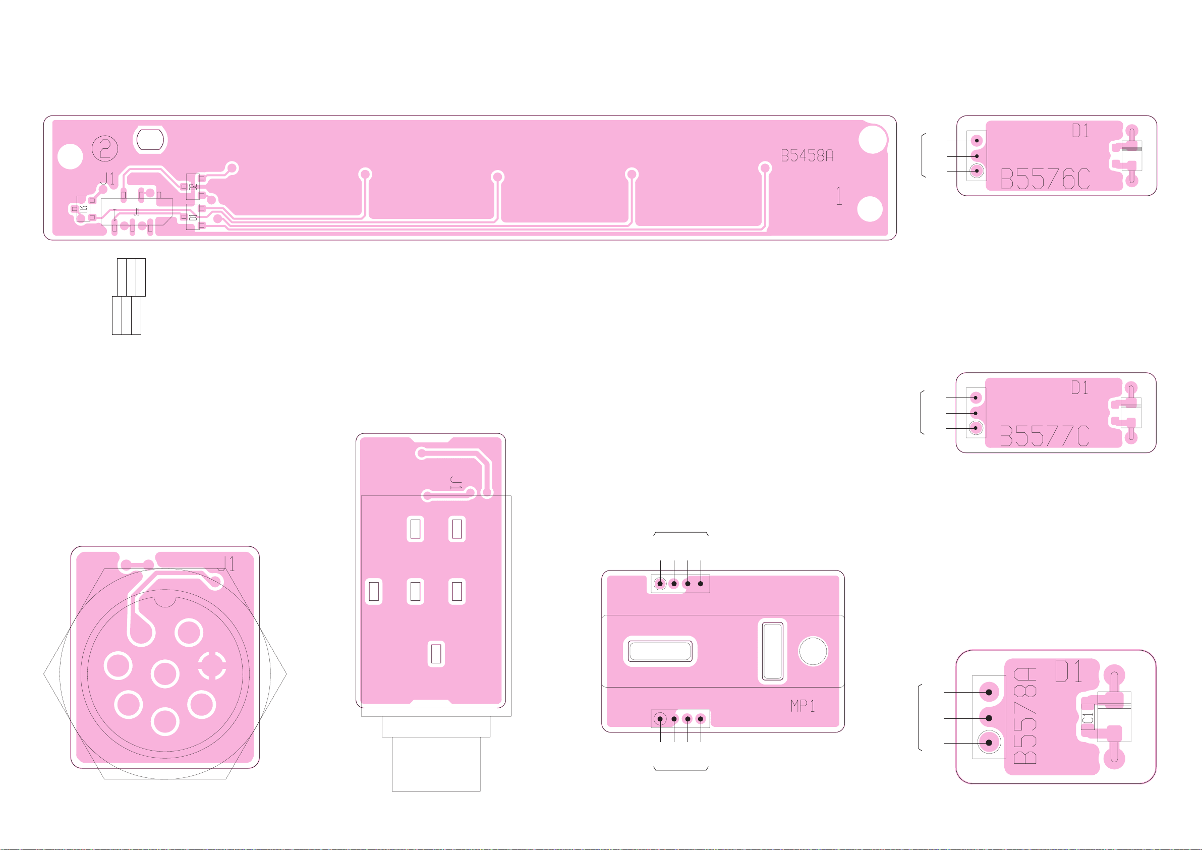
9 - 3
9-4 FUNC BOARD
• TOP VIEW
KST1
KST3
KRT1
KST2
J1
15
26
to DISPLAY unit J3
KRT0
GND
9-8 VARISTOR-A BOARD
• TOP VIEW
V-A2
GND
V-A1
to PA unit J652
9-5 MIC BOARD
• TOP VIEW
9-6 JACK BOARD
• TOP VIEW
9-7 DRV BOARD
• TOP VIEW
DRVO
DRVO
GND
GND
GND
GND
DRVI
DRVI
to PA unit J932
to PA unit J931
9-9 VARISTOR-B BOARD
• TOP VIEW
V-B2
GND
V-B1
to PA unit J653
9-10 VARISTOR-C BOARD
• TOP VIEW
V-C2
GND
V-C1
to PA unit J651
Page 80

9 - 4
• BOTTOM VIEW (VARISTOR-A BOARD)
• BOTTOM VIEW (VARISTOR-B BOARD)
• BOTTOM VIEW (VARISTOR-C BOARD)
• BOTTOM VIEW (FUNC BOARD)
• BOTTOM VIEW (MIC BOARD)
MIC
J2
210
19
to DISPLAY board J6
GND
PTT
MIUD
NC
MICE
AFO
MSQLS
+9V
GND
• BOTTOM VIEW (JACK BOARD)
PHIN
J2
51
62
to DISPLAY
board J5
SSPO
MSPO
GND
PHG
GND
• BOTTOM VIEW (DRV BOARD)
Page 81
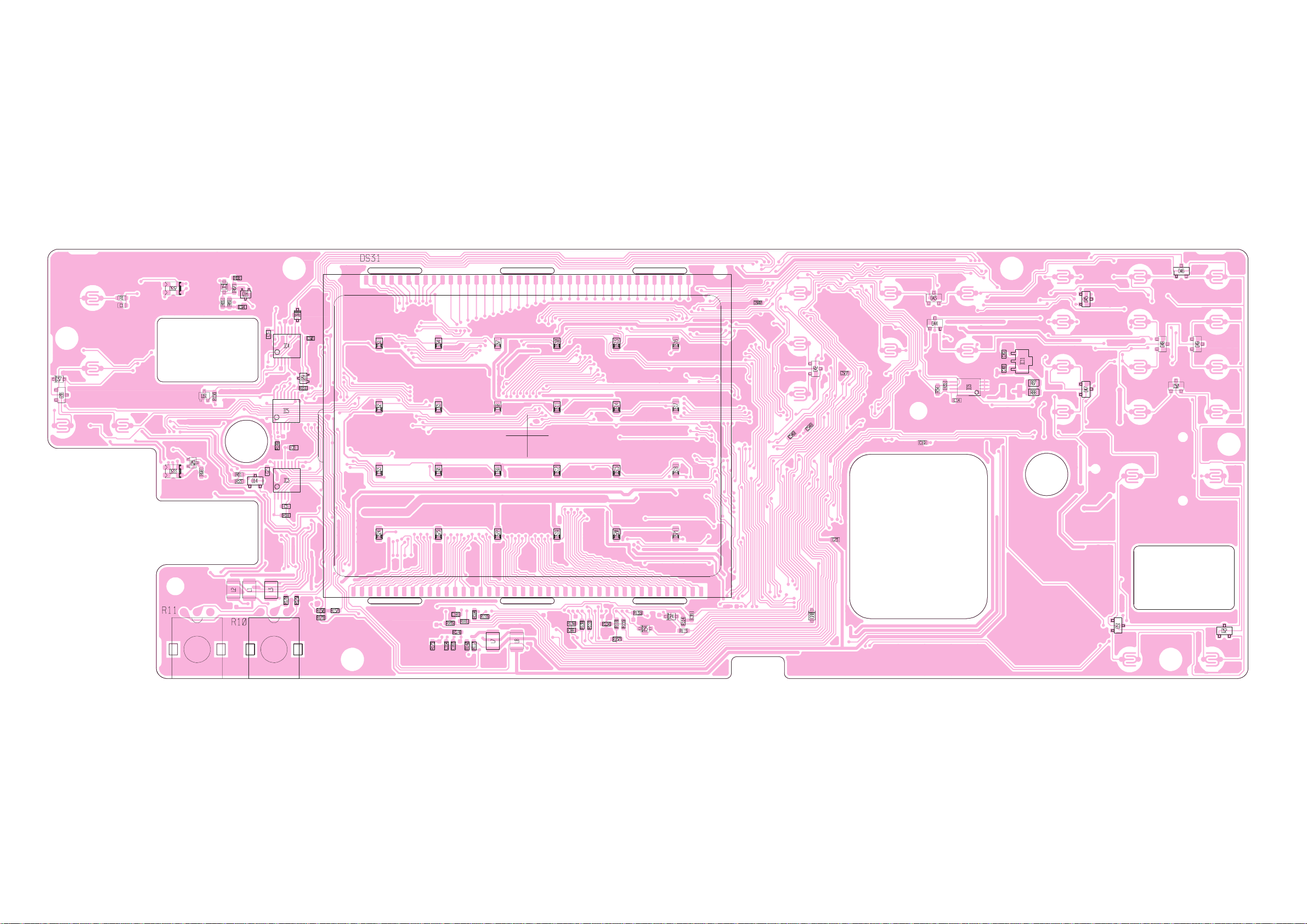
9 - 5
9-11 DISPLAY BOARD
• TOP VIEW
8
5
1
4
18
16 9
18
16 9
18
16 9
Page 82

9 - 6
• BOTTOM VIEW (DISPLAY BOARD)
1
4
5
8
1
548
14
85
1 100
81
80
5150
31
30
1
100
81
80
51
50
31
30
1
8
16
9
GND
1
to MAIN
SENSOR
J4
4
A
B
+5V
MSPO
J14
71
to MAIN unit
J1251, J1201
SSPO
PHG
14V
HV
MIC
MICE
to FAN
GND
J12
31
NC
F ANV
+5V
J2
1
to VR-A board J1
5
MSVR
NC
NC
MAVR
GND
2
6
PHIN
J5
SSPO
MSPO
GND
PHG
GND26
1
to JACK board J2
5
MIC
J6
1
to MIC board J2
9
GND
PTT
MIUD
NC
MICE
210
AFO
MSQLS
+9V
GND
GND
J9
19
to PLL unit J1
1
20 2
PDAT
43DT
14UL
GND
NC
NC
14V
+9V
-
5V
PCK
14DT
PST4
43UL
GND
BFST
14V
NC
NC
GND
INTS
J7
129
TXS
SCON
MDAT
+9V
AVXL
+5V
PCK
OPB1
12PS
12DS
12UL
12ST
12PV
GND
GND
INTM
RXS
MCK
NC
ETON
VOXL
NC
PDAT
FORL
ALCL
43PV
14PV
POWS
TEMP
2
to MAIN unit J1101
30
CIV
J8
129
to MAIN unit J1151
230
DRES
MIUD
ATXS
DOT
KDS
AGRM
NSQM
CTCM
CENS
SQLS
SMLS
MSC
-
5V
GND
GND
CIVE
PTT1
SEND
DASH
SBSY
CENM
SQLM
SMLM
BEEP
AGRS
NSQS
CTCS
OVDV
TONE
KST1
J3
51
to FUNC board J1
26
KST3
KRT1
KST2
KRT0
GND
GNDJ10 6
2
to RIT board J1
5
1
RIVR
NC
NC
SFVR
+5V
+5V
J11
1
5
to VR-B board J1
SSVR
NC
NC 2
6
SAVR
GND
Page 83

9 - 7
9-12 PA UNIT
• TOP VIEW
1
4
8
5
136
4
15
6
1
364
SPE
SP
J50
to MAIN unit J1853
SPE
SP
J51
1
2
2
1
to SP1
DRVI
DRVI
GND
GND
J931
14
to DRV board
GND
GND
DRVO
DRVO
J932
14
to DRV board
V-C1
GND
V-C2
J651
1
V-A2
GND
V-A1
J652
3
to
VARISTOR-A
board
to
VARISTOR-C
board
to
VARISTOR-B
board
V-B1
GND
V-B2
J653
1
313
14V
UTU1
UPRI
VUMS
UATT
POWS
REF
NC2
J39
1
15
2
16
to MAIN unit J1351
14V
5V
UT9V
UR9V
VUT9
FOR
43PV
GND
VUTP
J504
15
1
16
2
to MAIN unit J1301
14PV
VT9V
UR9V
UTU2
VPRI
VTU2
ICH
VTU1
GND
HV
VATT
GND
BAND
ICL
NC1
from PLL unit J251
144M 1Lo
P251
to MAIN unit J651
V SUB
P510
from PLL unit J551
430M 2Lo
P551
from PLL unit J421
430M 1Lo
P421
to MAIN unit J52
U MAIN
P1
to MAIN unit J652
U SUB
P30
to MAIN unit J51
V MAIN
P501
J2
UHF ANT
J1
VHF ANT
W305
VCC
GND
VCC
VCC
GND
GND
to UX-910
P300
F300
EP241
Page 84

9 - 8
• BOTTOM VIEW (PA UNIT)
1
3
4
6
1346
Page 85

9 - 9
9-13 PLL UNIT
• TOP VIEW
R325
1
25
75
4434
1222
18
169
33
23
1
11
51
10076
2650
1
4
8
5
1
25
75
33
23
1
11
22 12
34 44
51
10076
2650
1
4
8
5
14
85
GND
PDAT
43DT
14UL
NC
NC
NC
14V
+9V
-
5V
PCK
14DT
PST4
43UL
NC
BFST
14V
NC
NC
GND
1
2
J601
1
19
2
to DISPLAY board J9
to MAIN unit J501
to MAIN unit J1051
12
J701
to PA unit J503
J1
20
GND
BFOM
BFOS
GND
144M 1Lo
P251
to PA unit J240
430M 1Lo
P421
to PA unit J40
430M 2Lo
P551
from UX-910 J312
30.2
P312
Page 86

9 - 10
• BOTTOM VIEW (PLL UNIT)
R341
MP11
Page 87

9 - 11
9-14 MAIN UNIT
• TOP VIEW
1
18
16 9
1
10
20
18
16 9
11
8
18
169
18
169
169
18
16 9
8
1
18
16 9
8
16
9
1
1
8
16
9
14
85
1
169
18
12
24
13
18
16 9
16 9
1
18
16 9
18
16 9
8
14
85
1
1
8
16
9
7
14
8
8
1
18
16 9
18
16 9
1
12
REMOTE
ACC1DA TA1DA TA2
KEYMAIN SPSUB SP
MICE
MIC
J1201
12
to DISPLAY
board J14
NC
NC
GND
AFS
J1761
41
to UT-106
INTS
TXS
SCON
MDAT
9V
AVXL
5V
PCK
OPB1
12PS
12DS
12UL
12ST
12PV
GND
J1101
29
1
30
2
to DISPLAY
board J7
GND
INTM
RXS
MCK
NC
ETON
VOXL
NC
PDAT
FORL
ALCL
43PV
14PV
POWS
TEMP
GND
14V
NC
DRES
RXS
1FOR
OPB1
PCK
12ST
12DS
GND
GND
J2
2
24
1
25
to UX-910
IFM
NC
14V
GND
TXS
12TP
12PV
-
5V
PDAT
12PS
12UL
GND
IFS
NC1
ICL
BAND
GND
VATT
HV
GND
VTU1
J1301
15 1
16 2
to PA unit J504
ICH
VTU2
VPRI
UTU2
VR9V
VT9V
14PV
VUTP
GND
GND
5V
MDTC
INTM
J1771
19
210
to UT-106
GND
DSPM
MCKC
DPST
DRES
BFOS
GND
J1051
12
to PLL
unit J701
MSPO
SSPO
PHG
14V
HV
J1251
5
1
to DISPLAY
board J14
SPE
SP
J1853
2
1
to PA unit J50
DSOM
GND
GND
DSOS
J1802
1
4
to UT-106
AFM
GND
NC
NC
J1751
1
4
to UT-106
BFOM
GND
J501
12
to PLL unit J601
GND
43PV
FOR
VUT9
UR9V
UT9V
5V
14V
J1351
15 1
16 2
to PA unit J39
NC2
REF
POWS
UATT
VUMS
UPRI
UTU1
14V
SPST
MCKC
SPCE
SPCH
J1801
17
28
to UT-102
MDTC
BUSY
5V
GND
CIV
DRES
MIUD
ATXS
DOT
KDS
AGRM
NSQM
CTCM
CENS
SQLS
SMLS
MSC
-
5V
GND
J1151
30
2
29
1
to DISPLAY
board J8
GND
CIVE
PTT1
SEND
DASH
SBSY
CENM
SOLM
SMLM
BEEP
AGRS
NSQS
CTCS
OVDV
TONE
GND
GND
5V
MDTC
INTS
J1781
210
19
to UT-106
GND
DSPS
MCKC
DPST
DRES
from PA unit J30
USUB
P30
from PA unit J510
VSUB
P510
from PA unit J1
UMAIN
P1
from PA unit J501
VMAIN
P501
MP1
Page 88

9 - 12
• BOTTOM VIEW (MAIN UNIT)
14
85
1
7
1
1
12
814
71
814
7
1
5
10
6
1
5
10
14
8
1
7
7
1
8
814
71
14
6
1
14
85
24
13
7
14
8
14
85
14
8
Page 89

9 - 13
9-15 UX-910 MAIN UNIT
• TOP VIEW
IFM25
J311
to IC-910 MAIN
unit J2
NC
14V
GND
TXS
12TP
12PV
-
5V
PDAT
12PS
12UL
GND
IFS1
GND 24
14V
NC
DRES
RXS
1FOR
OPB1
PCK
12ST
12DS
12REF
GND 2
5
8
4
1
1
8
16
9
1
4
8
5
1
148
1
1
5
10
6
4
8
5
5
4
8
5
1
100
76
26
50
25
7551
1
3
6
4
14
85
4
1
5
5
8
4
1
136
4
8
1
4
8
5
12 ANT
to IC-910 PLL unit J541
SCLK
P312
W31
Chassis J1
to IC-910
PA unit
Page 90

9 - 14
• BOTTOM VIEW (UX-910 MAIN UNIT)
1
4
8
5
Page 91
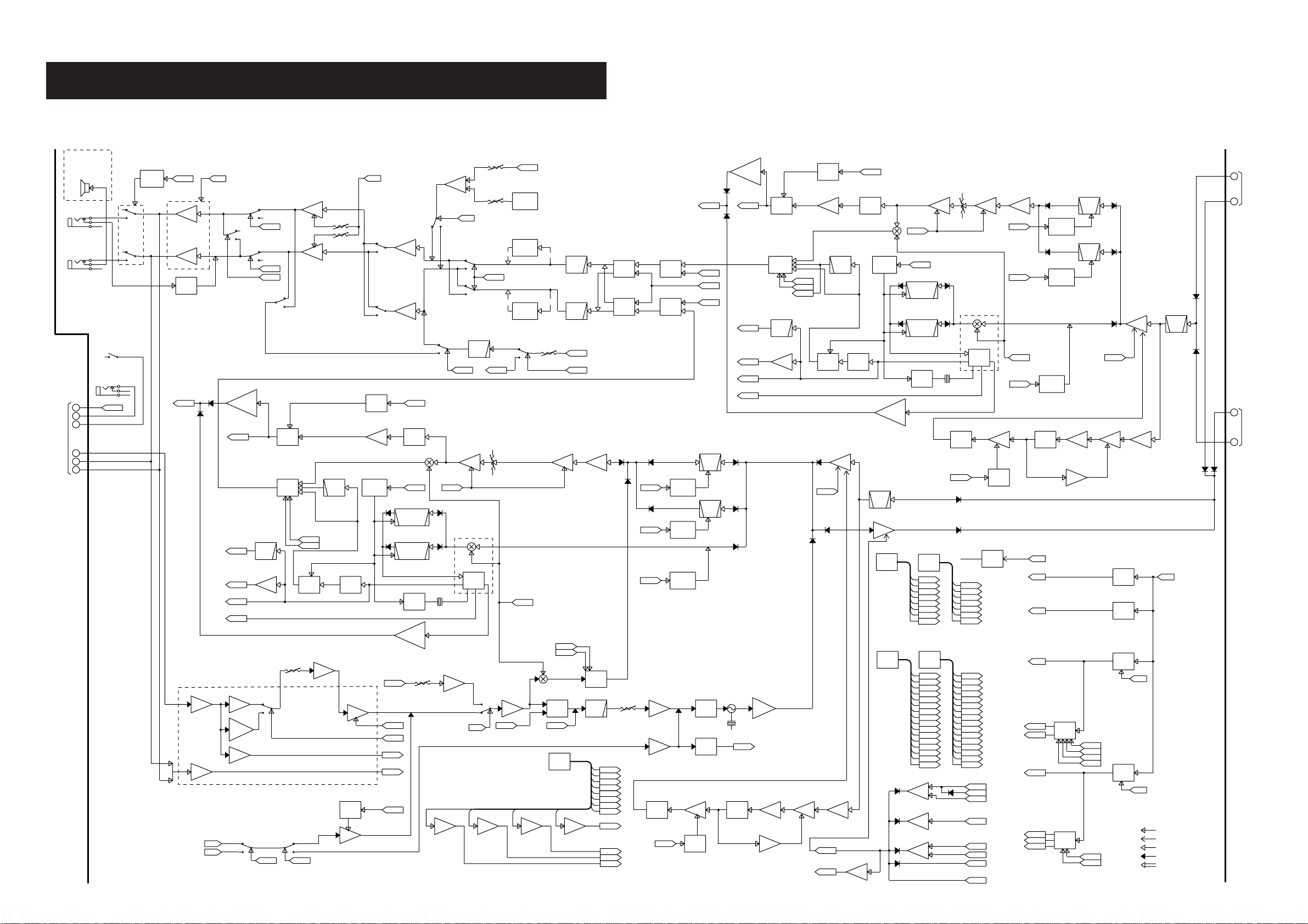
10 - 1
10-1 MAIN UNIT
SECTION 10 BLOCK DIAGRAMS
AF2S
AF1S
AF2M
AF1M
STLS
DSSW
DSPS
DSPM
UNFM
AGFM
AGSM
WNCM
COMS
CWVR
D96S
PIF
PHCO
PCON
MUTS
MUTM
EXTG
UPRI
430S
430M
430M
144M
UT9V
VT9V
VUT9
SW
SEND
REMOTE
COMMON LINE
LINE
RX LINE
TX LINE
DATA BUS LINE
DCON
DIN
MOD
BU4053BCFV
IC1531A
KEY
AVXL
EXTG
D96S
AMP
MICV
COMS
VOXL
VCA
NJM4565M
IC1654B
BU4053BCFV
IC1531C
BU4053BCFV
IC1531B
CTRL
GAIN
M62363FP
IC1803-5
MAIN UNIT
PIF
1750
BUFF
NBSM
TONE
BU4053BCFV
IC1653A
NJM2058M
IC1652C
2SC4116
Q1651
PRE-
NJM4565M
IC1651B
NJM4565M
IC1651A
Q52 2SC4116
Q107 XP4312
2SC4116
Q105
AMP
NB
DET
IF
AMP
AGC
AMP
IF
AMPIFAMP
EMPH
CTRL
NB
OVDV
BU4094BCFV
IC1481
REGIS-
SHIFT
UATT
VATT
ALUD
MICV
UTU2
UTU1
VTU2
VTU1
NJM2058M
NJM2058M
NJM2058M
IC1522B
IC1522C
IC1522A
NJM2058M
IC1522D
AMP AMP AMP AMP
RFGS
RFGM
DRVV
POCV
M62352GP
IC1521
D/A
LPF BUFF
FM
MOD
LIMIT
AMP
AMP
BU4094BCFV
BU4094BCFV
IC1461
IC1451
REGIS-
SHIFT
M62363FP
IC1803-7
NJM4565M
IC1654A
MA2S728
D1652
NJM2058M
IC1807D
1SV217
D253
FMW1
Q253
DTC144EU
Q106
SW
NB
1SS375
D371
XP4601
Q103
2SK882
Q101
LA1150N
IC101
2SK882
Q102
NJM2058M
IC1652A
CR-451
X251
2SC4116
Q254
DET
DEV
T9V
D0ST
SUST
MAST
PAST
SPST
DPST
D1ST
DCON
AGFS
AGSS
WNCS
NBSS
1FTS
1F2S
1F1S
NBSM
1FTM
1F2M
1F1M
RBDS
VPRI
144S
144M
430S
430M
144S
144M
UR9V
VR9V
D807
D805
Q817
Q816
Q804
BU4094BCFV
IC1511
TOR
REGIS-
SHIFT
TOR
BU4094BCFV
IC1491
BU4094BCFV
IC1471
TOR
REGIS-
SHIFT
TOR
Q811
2SA1588
Q812
DTC144EU
Q813
2SA1588
Q814
DTC144EU
Q815
2SA1588
D806
DAP222
SW
Q805
XP4312
Q806
DTC144EU
Q807
2SA1586
Q808
DTC144EU
Q809
XP4312
Q810
2SA1586
TXS
RXS
DA221
1SS355
2SC4116
2SC4116
2SD1801
REG
T9V
1ICL
ICH
ICL
14V
EALC
REG
R9V
Q801
2SD1664
Q831
DTC144EU
D804
DA221
BA09T
IC801
TA7805S
IC803
from UX-910
KDS
R9V
9V
5V
+5
REG
+9
REG
DTC144EUQ21
DTC144EUQ22
1SS355D21
CTRL
FORM
WAVE
1FTM
1F2M
1F1M
BUFF
IF
AMP
IF
AMP
DRIVER
DRIVER
DRIVER
XTAL
BPF
XTAL
BPF
AGCM
XTAL
BPF
IF
AMP
IF
AMP
1SS355
D207
DTC144EU
Q201
1SS355
3SK131
Q1
XP4312
Q153
XP4312
Q152
D201
CTRL
CAR
OPTION
FL-132
KDS
TCWS
WNCMDRIVER
CERAMIC
BPF
CERAMIC
BPF
HPF
BFOM
AF2M
AF1M
AGCM
NJM1496V
IC201
NJM2058M
IC1804C
DEEMPHA
TA31136FN (D)
IC401
CDBM455C24
X401
2SK1829
Q404
CTRL
DET
CFWS455HT
FI311
CFWS455E
FI312
DET
FM
AFRP
AF
AMP
OUTM
NSQM
CENM
CTCM LPF
AMP
NJM2058M
IC1652D
M62363FP
IC1803-6
NJM2058M
IC451C
XP401
Q405
SELECT
AF
2SK1829
Q406
SW
LEVEL
AF
µPC5023-077
IC1701
AMP
AMP
AMP
BUFF
BUFF
LIMIT
AMP
BU4053BCFV
IC1801A
BU4053BCFV
IC1653C
NJM2058M
IC1807C BU4053BCFV
IC452A
IC452B, IC452C
SELECT
AF
SMLM
CWVR
1750
LPF
LPF
LPF
1FTM
ETON
AGCM
NJM2058M
IC1652B
BU4053BCFV
IC1653B
M62363FP
IC1803-8
BU4053BCFV
IC1802A OPTION
BU4053BCFV
IC453A
NJM2058M
IC453B
NJM2058M
Q304 XP4312
Q303 XP4312
Q302 XP4312
CTRL
AGC
NJM2058M
IC1804D
UT-106
2SJ364
Q407
SQL
DSSW
SQLM
D302 MA728
NBSS
AMP
NB
DET
RFGM
AGC
AMP
AGC
DET
TA4101F
IC351
NJM2058M
IC451D
Q301 2SC4116
CTRL
GAIN
RF
1SS375
D303
2SC4116
Q305
XP4312
Q402
3SK131
Q352
3SK131
Q351
RV-110
R360
RX TOTAL GAIN
3SK131
Q51
XP4601
Q703
DTC144EU
Q706
SW
NB
2SC4116
Q350
XP4312
Q151
FL-211
FI51
FL-128
FI151
ALC
ALCL AMP
ALC
AMP
APC
AMP
APC
AMP
NJM2058M
IC1601A
NJM2058M
IC1601D
NJM2058M
IC1601C
NJM2058M
IC1601B
REF
FOR
POCV
1FOR
BFOS
1FTS DRIVER
DRIVER
DRIVER
XTAL
BPF
XTAL
BPF
AGCS
BPF
IF
AMP
XP4312
Q753
3SK131
FL-212
FI651
2SC4116
Q705
1SS375
D701
2SK882
Q701
LA1150N
IC701
IF
AMP
AGC
AMP
IF
AMPIFAMP
2SK882
Q702
2SJ364
Q1002
SQL
SQLS
AF2S
TA31136FN (D)
NJM2085M
IC1804A
2SK1829
Q1001
CFWS455E
FI512
CFWS455HT
FI511
2SK1829
Q952
CDBM455C24
X951
SW
LEVEL
AF
EMPHA
DE-
CTRL
DET
DET
FM
IC951
Q707 XP4312
Q652 2SC4116
CTRL
NB
BU4053BCFV
IC1002A
SELECT
AF
MSC
DSSW
NSQS
OUTS
CENS
CTCS
LPF
AMP
BEEP
BU4053BCFV
IC1801C
NJM2058M
IC1807A
M62363FP
IC1803-3
M62363FP
IC1803-2
OPTION
BU4053BCFV
IC1802C
BU4053BCFV
IC1802B
OPTION
XP4601
Q953
NJM2058M
IC1001C
IC1001A
NJM2058M
IC1001B
NJM2058M
UT-102
UT-106
BU4053BCFV
IC1801B
NJM2058M
IC1807B
PHCO
ATX209
1SS355
D1851
DTC144EU
Q1855
DRIVER
AF
AMP
AF
AMP
AF
AMP
AF
AMP
AF
AMP
ATT
RL1851
MAIN EXT SP
SUB EXT SP
C065K12I0810
SP1
COVER UNIT
LA4445
IC1852
BU4053BCFV
IC1806C
IC1002B IC1002C
SMLS
5V
14V
PCON
MUTM
MUTS
AGCS
AGC
AMP
AGC
DET
METER
AMP
METER
AMP
METER
AMP
METER
AMP
M62363FP
IC1803-4
M62363FP
IC1803-1
BU4053BCFV
IC1806B
BU4053BCFV
IC1806A
M5282FP
IC1809
M5282FP
IC1808
VCA
VCA
BU4053BCFV
NJM2058M
IC1804B
Q905 XP4312
Q904 XP4312
Q903 XP4312
CTRL
AGC
SELECT
AF
AFRP
RFGS
AF1S
HPF DRIVER
WNCS
CERAMIC
BPF
CERAMIC
BPF
AGCS
NJM2058M
IC1001D
XP4312
Q951
D903 MA728
Q902 2SC4116
RF
GAIN
CTRL
2SC4116
Q901
1SS375
D902
TA4101F
IC851
RV-110
R857
3SK131
Q852
3SK131
Q851
1F2S
1F1S
BUFF
IF
AMP
IF
AMP
2SC4116
Q850
XP4312
Q752
XP4312
Q751
OPTION
FL-133
FL-129
FI751
Q651
A
to
FRONT
UNIT
B
C
D
E
F
J
I
H
G
to
PA
UNIT
to
PA
UNIT
Page 92

10 - 2
10-2 PA AND PLL UNITS
B2LO
60.4 MHz
OSC BUFF
AMP
AMP
AMP
2SC4081
2SC4081
Q602
Q541
SC-1287
IC601
2SC5107
Q551
x2
BPF
ATT LPF
DDS
BFOM
to UX-910
30.2 MHz
COMMON LINE
LINE
RX LINE
TX LINE
DATA BUS LINE
43UL
DTC144EU
Q154
DET
UNLOCK
BFOS
ATT
ATT
LPF
LPF
HPF
HPF
from DISPLAY BOARD
BU4094BCF
IC1
DRIVER
RV-148
R570
2SC4081
Q702
2SC4081
Q501
(30.2 MHz)
CR-293
OPTION
CR-452
X512
SC-1287
IC701
2SC5107
Q472
2SC5107
Q471
SC-1246A
IC331
MA357
µPC4570
IC12A
µPB1509GV
IC471
DDS
DDS AMP 1/8 BUFF
B1LO
348.75 MHz
-
408.75 MHz
KICK
KICK
Q161
DTA144EU
Q361
DTA144EU
µPC4570
IC161A
SC-1246A
IC131
2SC5107
Q392
µPC4570
IC12B
MA357
MA357
MA357
D394
D393
D392
D391
2SK1577
Q391
2SC4081
Q271
AMP
BUFF
BUFF
LPF
1/8
µPB1509GV
IC271
2SC5107
Q272
2SC4081
Q261
MA357
MA357
MA357
MA357
D194
D193
D192
DDS
14UL
DET
UNLOCK
DTC114EU
Q153
43LV
9V
1SS355
D381
Q381
RIPPLE
FIL
2SD2345
1SS355
D181
Q181
RIPPLE
FIL
2SD2345
UR9V
XP4312
XP4312
Q282
Q281
2SK508
Q11
PA UNIT
14LV BUFF BUFF
BUFF
BUFF
LOOP
FIL
LOOP
FIL
UTU1
BPF
5V
+5
REG
14V
IC501
FL-130
FI281
2SC3356
Q221
2SC3356
Q220
TA7805F
14V
UTU2
UT9V
UATT
µPC4570
IC161B
D191
2SK1577
Q191
2SC5107
Q192
1SS301
D80
2SC2712
Q261
PLL UNIT
POWS
A1LO
LPF ATT
LPF ATT
DAN202U
D303
DTC114EU
Q300
ALD112
RL300
DRIVERDRIVER
125.15 MHz
-
163.15 MHz
DC INPUT
REF
FOR
UPRE
FGB 4A
F300
HSU88
D181
HSU88
D180
DTC114EU
Q183
DTC114EU
Q703
2SB1132
Q702
PQ20VZ51
IC701
REG
430 MHz
HV
VCC
VCC
ATTBPF
PRE
AMP
VCC
UT9V
VT9V
UT9V
LPF
DRIVER
TX/RX
SW
PWR
AMP
PAHV
ICH
ICL
1SV286
1SV286
1SV286
D262
D261
D260
3SK177
Q260
1SV286
D263
1SV237
D264
SRFJ7044
Q131
2SK2975
Q930
BOARD
DRV
2SK2973
Q121
2SC3102
2SC3102
Q152
Q151
1SS301
D680
CPH3404
Q656
SW
MA4FH224
XB15A407
XB15A407
XB15A407
XB15A407
XP4312
Q180
D265
MA4FH224
D266
D185
D184
D183
D182
DET
IC
Q203 DTC114EU
BAND
B2LO
ATT
BPF
DRIVER
DRIVER
LO
AMP
HPF
B1LO
1SV286
1SV286
D642
D641
BPF
BPF
ATT
FL-131
FI280
XTAL
BPF
XTAL
BPF
µPC2710
IC240
2SC3357
Q200
µPC2710
IC200
LFSC25N 12B 0440B
FI202
LFSC25N 12B 0440B
LFSC25N 12B 0440B
FI201
FI200
Q202 XP4312
CTRL
FILTER
2SK2854
Q101
ATT
LPF
LPF
LPFLPFLPF
ATTLPFATT
LO
AMP
HPF
VUMS
VTU2 VTU1
UR9V
UT9V
LPF
LPF
HPF
BPF
LPF
ATT
ATT
ATT
ATT LPF
ATT
BPF
BPF
LPF
DRIVER
VT9V
DTC144EU
XP4312
Q21
BUFF
DTC144EU
DTC144EU
Q33
Q32
Q30
µPC2709
IC40
HSB88WS
D190
2SC2714
Q3
RF
AMP
2SK302
Q2
2SK302
Q1
VR9V
A1LO
HPF
1SV286
1SV286
DTC144EU
DTC144EU
DTC144EU
Q508
Q506
Q505
DRIVER
µPC2710
IC502
2SK1740
2SK1740
Q512
Q511
1SV286
2SK302
2SK302
D502
Q502
Q501
LPF LPF HPF ATT
ATT
LPF
LO
AMP
D504
D503
VTU1
VTU2VTU1
1SV217
1SV217
1SV217
1SV217
µPC2709
IC501
YGR
AMP
YGR
AMP
YGR
AMP
D512
D511
D510
BPF
PRE
AMP
D513
BPF
3SK177
Q507
VATT
VT9V
ATT
PWR
AMP
TX/RX
SW
DRIVER
DRIVER
VT9V
LPF
SWR
DET
PREAMP
SW
PREAMP
SW
SWR
DET
2SC5125
2SC5125
Q652
Q651
MA29B
D651
MA29B
D650
2SD1585
Q650
CPH3404
Q658
SW
BIAS
LPF
DRIVE
AMP
PRE
DRIVE
RF
AMP
RF
AMP
HPF
HSM88AS
D514
LIMIT
1SV237
D515
2SC2712
Q515
DTC144EU
Q510
XP4312
Q700
1SV265
D710
AE5349
RL700
VPRE
HSU88
D721
HSU88
D720
2SB1132
Q182
144 MHz
CHASSIS
UNIT
PLL DATA
J
I
H
G
to
MAIN
UNIT
to
MAIN
UNIT
Page 93

10 - 3
10-3 FRONT UNIT
S-80942ANMP-DD6
IC7
ALCL
STL
SRL
KEY
FRONT
RMS20-250-201-1R
EP1
XN58X2464
IC6
MAIN SENSOR
KEY MATRIX BUS
FRONT
KEY
FUNC BOARD
SUB
TX/RX
LED
PHIN
SFVR
RIVR
SSVR
SAVR
MSVR
MAVR
PHONE
JACK
VR-A BOARD
VR-B BOARD
RIT BOARD
MAIN
TX/RX
LED
COMMON LINE
LINE
RX LINE
TX LINE
DATA BUS LINE
SHIFT VR
RIT VR
SUB
RF/SQL VR
SUB
AF VR
MAIN
RF/SQL VR
MAIN
AF VR
MTL
MRL
Q20
DTC114TU
Q21
DTC114TU
Q18
DTC114TU
Q19
DTC114TU
IC8
TC7W08F
LED
CTRL
LED
CTRL
EEPROM
DRIVER
DRIVER
DRIVER
MC16C/62FP
IC1
CPU
MIUD
PHIN
FORL
CENS
CENM
VUTP
OVDV
NSQS
NSQM
VOXL
AVXL
43LV
14LV
HV
BU4052BCFV
BU4052BCFV
IC5
IC4
(14.7456MHz)
CR-636
X1
SED1540F
IC2
2SD1664
Q1
SIG OUTSIG IN
A/D LINE
MULTI
MULTI
RESET
14V
FAN2
FAN3
FAN1
H5V
+5
REG
FAN
CTRL
-
5
DC-DC
-
5V
IC11
AN78L05M
IC201
NJM2360M
D202
SB07-03C
TLGE1002
DS1
-
DS24
A0095
DS31
BACK LIGHT
LCD
HV
Q22
DTA144EU
Q23
DTA144EU
Q24
2SB1201
Q25
2SC4116
Q26
DTA144EU
D17
MA8082 M
MF1
SB0812H-ICOM-00
FAN
SFVR
RIVR
POVR
MIVR
SSVR
MSVR
SAVR
MAVR
SMLS
SMLM
BU4052BCFVIC3
SIGNAL BUSSIGNAL BUS
MULTI
FRONT UNIT
CHASSIS UNITDISPLAY BOARD
IC9
TC7W04F
Q12
2SA1586
Q13
2SC4116
D13
1SS355
Q17
2SC4116
D16
1SS355
DATA BUS
PLL
DATA BUS
MAIN
CI-V
I/F
TO MAIN UNIT
SEND
CTRL
SEND
CTRL
MIUD
MIC
JACK
Q16
2SC4116
D15
1SS355
JACK BOARD
MIC BOARD
A
to
MAIN
UNIT
B
C
D
E
F
10-4 UX-910
12AT
CNTY
14V
IC161: BA09T
IC162: TA7805F
REG
+9
REG
+5
+5
+9
R+5
D169: MA2S111
Q172: RN2425
CTRL
R+5
D167: DAN222
Q169: XP4315
CTRL
REG
12S
12M
Q301: XP1113
SW
12M
12S
RXS
IC301: BU4094
12DS
CK
DAT
12PR
12DR
12C2
TC7W74FU
IC610:
IC311: TC7W08F
BUFF
CK
DAT
PCK
PDAT
SCLK
Q601: 2SC4215
30.2 MHz
TC7SU04F
IC601:
IC661:
SC-1246A
DDS
AMP
LPF
AMP
IC701: µPC4570
D711, D712: 1SV214
Q731: 2SC5107
2SC5107
Q761:
TC7S04F
IC762:
IC761: µPB1509GV
Q741:
2SC5107
FILTER
LOOP
2LO
SUB: 232.95 MHz
-
233.05 MHz
MAIN: 233.0 MHz
-
233.15 MHz
15.1 MHz
12M
TXS
Q170: 2SB1132
Q167: DTA144EU
Q165: XP4315
Q168: 2SC2712
D166: 1SS355
Q166: 2SB1133
CTRL
REG
REG
T9V
REG
R9V
1RX9
1TX9
T+5
D168: MA2S111
Q171: RN2425
CTRL
T+5
Q681: 2SC5107
2SC5107
Q551:
Q512: 2SC4116
Q511: 2SK880
IC502: TC7W66PU
Q542: 2SC5193
Q541: 2SC5508
IC501:
TB31242
PLL
ATT
AMP
ATTLPF
AMP
1/8
1/2
BUFF
AMP
FIL
LOOP
IC201:
µPC2709
CK
DAT
Q221:
3SK166
MAIN DAT
10.95 MHz
IFS
FI241
243.95 MHz
(SAW)
IC241:
FI271:
UPC2721
Q282: 2SC2712
12AT
SW
Q271:
LFSN30N18C1280BLFSN30N18C1280B
FI281:
IC181:
2SC5454
µPC2709
1LO: 996-1076.1 MHz
Q281:
NE34018
Q71: 2SD1801
Q72: DTC144EU
Q74: 2SC2712
Q73: 2SC2712
12PR
LPF
LPFAMP
DRIVE
AMP
PRE
DRIVE
APC
AMP
HVR
CTRL
PRE
D503: HSU88
D502: HSU88
1TX9
DET
POWER
Q36: 2SK2354
M57762-02
IC21:
2SK2855
Q38
PA
IC141:
LFSN30N18C1280B
FI1:
µPC8163TB
LFSN30N18C1280B
FI141:
IC131:
WF447B
IC111:
FI101:
243.95 MHz
µPC2709
2SC2712
Q81:
D82: HSB88WS
10.85 MHz
AMP LPF
ATT ATT ATT ATT ATT BPF
YGR
AMP
BPF BPF LPF
ATT
LPF
IF
AMP
IFM
1FOR
ATT
ATT
ATT
LPF
BPF
ATT
BPF
LPF
ATT
HPF
BPF
BPF
BUFF
HPF
LO
AMP
RF
AMP
RF
AMP
LPF
ATT
AMP
IC31: BA4558F
IC2
IC1
COMMON LINE
LINE
RX LINE
TX LINE
DATA BUS LINE
:
µPC1878G
Page 94

11 - 1
SECTION 11 WIRING DIAGRAM
12
J551
J541
30.2
P312
J1
20
19
18
17
16
15
14
13
12
11
10
9
8
7
6
5
4
3
2
1
PLL UNIT
430M 1Lo
W305
2
1
2
1
GND
BFOS
J1051
2
1
P701
2
1
AFS
DSOM
GND
GND
DSOS
GNDNCNC
DRES
INTS
DPST
MDTC
MCK5VDSPS
GND
GND
GND
IFM
GNDNCNC
14V
14V
GND
DRES
TXS
RXS
12TP
1FOR
12PV
OPB1
-
5V
PCK
PDAT
12ST
12PS
12PS
12UL
GND
GND
GND
IFS
J1781
P1761
J2
J1802
P1781
4
432
1
432
1
123456789
10
123456789
101112131415161718192021222324
25
GND
GND
BFOM
BFOS
GND
BFOM
J501
2
1
P601
2
1
J701
2
1
J601
2
1
SPE
J40
J503J240
J251J421
SPE
NC2
1Lo
430M
1Lo
144M
1Lo
430M
1Lo
430M 2Lo
GND
144M
2Lo
430M
SP
GND
43PV
REF
FOR
POWS
VUT9
UATT
UR9V
VUMS
UT9V
UPRI
5V
UTU1
14V
14V
DRVI
DRVI
GND
GND
DRVO
DRVO
GND
GND
NC2
P50
1
2
J50
1
2
GND
43PV
REF
FOR
POWS
VUT9
UATT
UR9V
VUMS
UT9V
UPRI
5V
UTU1
14V
14V
SP
J1853
2
1
87
65
43
21
SPCHGND
NC1
BAND
J39
16
15
14
13
12
11
10
9
8
7
6
5
4
3
2
1
J1351
16
15
14
13
12
11
10
9
8
7
6
5
4
3
2
1
ICH
ICL
VTU2
VPRI
GND
UTU2
VATT
VR9V
HV
VT9V
GND
14PV
VTU1
VUTP
J504
16
15
14
13
12
11
10
9
8
7
6
5
4
3
2
1
J1301
16
15
14
13
12
11
10
9
8
7
6
5
4
3
2
1
V-C2
GND
V-C1
J651
3
2
1
VARISTOR-C
BOARD
V-B2
GND
V-B1
J653
3
2
1
VARISTOR-B
BOARD
V-A2
GND
V-A1
J652
3
2
1
VARISTOR-A
BOARD
NC1
BOARD
DRV
BAND
SP
SPE
ICH
ICL
VTU2
VPRI
GND
UTU2
VATT
VR9V
HV
VT9V
GND
14PV
VTU1
VUTP
PA UNIT
UNIT
COVER
J1
2
1
J51
1
2
SP1
HV
GND
VHF ANT
CHASSIS J1
UHF ANT
CHASSIS J2
GND
VCC
P300
1
2
3
4
5
6
GND
VCC
J932
1
2
3
4
J931
4
3
2
1
USUB
UMAIN
VMAIN
VSUB
USUB
UMAIN
VMAIN
VSUB
P510
J510
J652
J52
J51
J651
J501
J1
J30
P30
P251P421 P551
P1
P501
MCKC
SPCE
SPST
5V
BUSY
MDTC
J1801
87
65
43
21
[DATA1]
J1561
6
5
1
1
3
4
2
6
5
1
3
4
2
[KEY]
J1401
[DATA2]
J1571
[SUB-SP]
J1852
[MAIN-SP]
J1851
J1751
432
1
3
2
1
432
1
P1771
DRES
INTM
DPST
MDTC
MCKC5VDSPM
GND
GND
GND
AFM
GNDNCNC
J1201
2
1
MICE
MIC
J1771
123456789
10
J1251
5
4
3
2
1
HV
14V
PHG
SSPO
MSPO
GND
CIV
CIVE
DRES
PTT1
MIUD
SEND
ATXS
DASH
DOT
SBSY
J1151
30
29
28
27
26
25
24
23
22
21
20
19
18
17
16
15
14
13
12
11
10
9
8
7
6
5
4
3
2
1
SMLM
SMLS
KDS
CENM
AGRM
SQLM
NSQM
CTCM
BEEP
CENS
AGRS
SQLS
NSQS
CTCS
MSC
OVDV
-
5V
TONE
GND
GND
CIV
CIVE
DRES
PTT1
MIUD
SEND
ATXS
DASH
DOT
SBSY
SMLM
SMLS
KDS
CENM
AGRM
SQLM
NSQM
CTCM
BEEP
CENS
AGRS
SQLS
NSQS
CTCS
MSC
OVDV
-
5V
TONE
GND
GND
INTS
INTM
TXS
RXS
SCON
MCK
MDAT
NC
9V
ETON
AVXL
VOXL
5V
NC
PCK
PDAT
OPB1
J1101
30
29
28
27
26
25
24
23
22
21
20
19
18
17
16
15
14
13
12
11
10
9
8
7
6
5
4
3
2
1
1
2
3
4
5
6
7
8
9
10
11
12
13
14
15
16
17
18
19
20
21
22
23
24
25
26
27
28
29
30
1
2
3
4
5
6
7
8
9
10
11
12
13
14
15
16
17
18
19
20
21
22
23
24
25
26
27
28
29
30
FORL
12PS
ALCL
12DS
43PV
12UL
14PV
12ST
POWS
12PV
TEMP
GND
GND
INTS
INTM
TXS
RXS
SCON
MCK
MDAT
NC
+9V
ETON
AVXL
VOXL
+5V
NC
PCK
PDAT
OPB1
FORL
12PS
ALCL
12DS
43PV
12UL
14PV
12ST
POWS
12PV
TEMP
GND
[REMOTE]
J1403
[ACC]
J1581
6
5
1
8
3
4
2
7
6
5
8
3
4
2
7
CIVE
NC
CIV
SQL
13.8V
NC
ALC
SEND
MOD
GND
AF
SQL
DOUT
GND
DIN
PTT
AF
SQL
DOUT
GND
NC
NC
AF
GND
DOT
DASH
GND
INSPM
EXSPM
GND
INSPS
EXSPS
GND
-
5V
NC
+9V
NC
14V
14V
NC
BFST
NC
NC
NC
43UL
14UL
PST4
43DT
14DT
PDAT
PCK
GND
GND
-
5V
NC
+9V
NC
14V
14V
NC
BFST
NC
NC
NC
43UL
14UL
PST4
43DT
14DT
PDAT
PCK
GND
FAN
M
+
-
J14 P1201
7
6
5
4
3
2
1
7
6
5
4
3
2
1
HV
14V
MIC
MICE
MSPO
PHG
SSPO
PHG
PHIN
GND
SSPO
MSPO
GND
MIC
MICE
+9V
MIUD2
GND
AFO
PTT
MSQLS
GND
J6
10
9
8
7
6
5
4
3
2
1
J5
6
5
4
3
2
1
+5V
A
B
J4
4
3
2
1
SENSOR
TO MAIN
GND
PCK
PDAT
J8
+5V
RIVR
SFVR
KRT1
KRT0
KST3
KST2
KST1
J3
6
5
4
3
2
1
J10
6
5
4
3
2
1
+9VP
+14VP
+14VP
14DT
43DT
PST4
14UL
43UL
GND
GND
BFST
NC
NC
NC
NC
-
5V
GND
GND
PCK
PDAT
+9VP
+14VP
+14VP
14DT
43DT
PST4
14UL
43UL
GND
GND
BFST
NC
NC
NC
NC
-
5V
GND
J9
20
19
18
17
16
15
14
13
12
11
10
9
8
7
6
5
4
3
2
1
+5V
+5V
SAVR
SSVR
MAVR
MSVR
J2
6
5
4
3
2
1
J11
6
5
4
3
2
1
GND GND
MAVR
MSVR
+5V
NC
NC
NC
NC
NC
NC
NC
NC
J1
6
5
4
3
2
1
GND GND
SAVR
SSVR
J1
6
5
4
3
2
1
+5V
J1
6
5
4
3
2
1
GND
RIVR
SFVR
+5V
NC
NC
GND
GND
NC
NC
PHIN
GND
SSPO
PHG
MSPO
GND
J2
1
2
3
4
5
6
J1
J2
10
1
2
3
4
5
6
7
8
9
MSQLS
GND
NC NC
+9V
MIUD
PTT
AFO
GND
MICE
MIC
1
2
3
4
5
6
7
8
J1
GND GND
KRT1
KRT0
KST3
KST2
KST1
J1
6
5
4
3
2
1
J12 P1
3
2
1
3
2
1
GND
NC
FANV
GND
NC
FANV
MF1
CHASSIS
J7
(OPTION)
UT-106
(OPTION)
UX-910
MAIN UNIT
(OPTION)
VOICE UNIT
UT-102
(OPTION)
UT-106
DISPLAY BOARD
VR-A BOARD
VR-B BOARD
RIT BOARD
JACK BOARD
MIC BOARD
FUNC
BOARD
Page 95

12 - 1
12-1 FRONT UNIT
SECTION 12 VOLTAGE DIAGRAMS
[POWER]
J14
from MAIN
unit J1251,
J1201
to MAIN
unit J1101
to MAIN
unit J1151
7
6
5
4
3
2
1
HV
14V
MIC
MICE
MSPO
PHG
SSPO
PHG1
HF50ACC322513-B
L3
PHIN
GND
SSPO
MSPO
GND
MIC
MICE
+9V
MIUD2
GND
AFO
PTT
MSQLS
GND
J6
10
9
8
7
6
5
4
3
2
1
0.001
C25
EP4
HF50ACC322513-B
L5
EP1
HF50ACC322513-B
L2
2.2k
R60
100k
R59
MIC
MICE
MSPO
PHG
0.001
C34
0.001
C33
0.001
C32
0.001
C31
0.001
C30
0.001
C29
0.001
C27
EP3
EP2
HF50ACC322513-B
DISPLAY BOARD
L4
DAP202K
D14
47k
R61
MIUD1
MITX
43PV1
14PV1
SEND2
SEND1
AGRS1
AGRM1
POWS1
DASH1
DOT1
ACUD
+9V
PTT
0.1
C94
1k
R66
1SS355
D15
2SC4116
Q16
47k
R69
820
R68
2.2k
R67
STLE
SRLE
MTLE
0.1
C36
1k
R71
1SS355
D16
2SC4116
Q17
820
R73
2.2k
R72
47k
R70
H5V
DTC114TU
Q21
DTC114TU
Q20
DTC114TU
Q19
10
C50
0.1
C49
AN78L05M
IC11
DRES1
MSC1
MDAT1
MCK1
FAN3
STL
SRL
MTL
MRL
FAN2
FAN1
FRST
47k
R185
EP5
10
C47
0.1
C48
120
R88
120
R87
BU4094BCFV
IC10
15
OENA
16
VDD
14
Q5
13
Q6
12
Q7
11
Q8
10
Q'S
9
QS
8
VSS
7
Q4
6
Q3
5
Q2
4
Q1
3
CLK
2
DATA
1
STRB
PCK1
PDAT1
OPB11
12PS1
ALCL1
12DS1
43PV1
12UL1
14PV1
12ST1
POWS1
12PV1
TEMP1
FORL1
220
R167
220
R172
18k
R176
18k
R140
100k
R173
100k
R175
100k
R174
RB706F-40
D31
1SS385
D10
220
R170
220
R166
220
R171
220
R169
220
R168
220
R165
1
R158
220
R156
PCK
PDAT
GND
TEMP
12PV
POWS
12ST
14PV
12UL
43PV
12DS
ALCL
12PS
FORL
OPB1
220
R181
220
R164
220
R163
+5V
VOXL
AVXL
ETON
+9V
MDAT
MCK
SCON
RXS
TXS
INTM
INTS
GND
0.001
C75
J7
30
29
28
27
26
25
24
23
22
21
20
19
18
17
16
15
14
13
12
11
10
9
8
7
6
5
4
3
2
1
HF50ACC322513-B
L8
100k
R112
220
R128
220
R127
INTS1
INTM1
TXS1
220
R151
RXS1
SCON1
MDAT1
MCK1
ETON1
AVXL1
VOXL1
18k
R150
18k
R117
220
R184
0.001
C74
100k
R111
0.47
C57
100k
R19
220
R182
220
R157
220
R154
220
R153
220
R152
220
R110
220
R109
COM1
COM2
COM3
COM4
SG73
HF50ACC322513-B
L7
10k
+9V
5V
5V
R80
1.2k
R83
10k
R81
10k
R82
0.1
C46
DTC114TU
Q18
0.1
C42
0.1
C41
MRLE
MPSB
MPSA
TST0
0.1
C549
0.1
C548
0.1
C547
0.1
C541
0.1
C542
0.1
C538
0.1
C536
PHIN1
RXD
TXD
PTXS
ATXS1
SQLS1
SQLM1
PDAT1
43PV1
PCK1
14PV1
DRES1
PTT11
AGRS1
AGRM1
INTS1
INTM1
POWS1
DASH1
DOT1
CIVE
CIV
SSPO
W2
0.1
C23
2SC4116
Q13
2SA1586
Q12
1SS355
D13
18k
R58
47k
R57
33k
R56
6.8k
R55
47k
R54
TC7W04F
IC9C
3 5
TC7W04F
IC9B
6 2
TC7W04F
IC9A
4
8
1 7
J5
6
5
4
3
2
1
HF50ACC322513-B
L1
0.001
C24
2.2k
R53
1k
R52
100k
R51
+5V
A
B
0.001
C19
220k
R48
100k
R47
220k
R44
100k
R43
J4
4
3
2
1
SENSOR
to MAIN
0.1
C213
0.001
C16
TC7W08F
IC8B
3
4
6
5
TC7W08F
IC8A
8
7
2
1
0.1
C21
100p
C22
100p
C20
12p
C18
12p
C17
X1 : CR-636
1M
R50
100k
R49
1M
R46
100k
R45
(14.7456 MHz)
SEND2
BFST1
KDS1
BEEP1
ETON1
12PV1
MDIB
MDIA
0.1
C527
0.1C37
100k
R42
100k
R40
KST3
KST2
KST1
KST0
KRT7
KRT6
KRT5
KRT4
KRT3
KRT2
KRT1
KRT0
LCD7
LCD6
LCD5
LCD4
LCD3
LCD2
0.1
C39
WR
RD
LCDC
LCDA
SG01
SG02
SG03
SG04
SG05
SG06
SG07
SG08
SG09
SG10
SG11
LCD1
LCD0
2.2M
R78
47k
R79
SG68
SG67
SG66
SG65
SG64
SG63
SG62
SG61
SG60
SG59
SG58
SG57
SG56
SG55
SG54
SG69
SG70
SG71
SG72
SEND1
ATXS1
DASH1
DOT1
SBSY1
KDS1
CENM1
AGRM1
SQLM1
NSQM1
SMLM1
CTCM1
BEEP1
CENS1
AGRS1
SQLS1
NSQS1
SMLS1
CTCS1
MSC1
OVDV1
TONE1
RB706F-40
D34
RB706F-40
D29
RB706F-40
D27
RB706F-40
D28
RB706F-40
D35
0.001
R141
220
R160
1M
R139
220
R136
220
R132
220
R131
1M
C89
330p
C182
C181
C163
C164
C168
330p
330p
330p
330p
0.001
C88
1SS355
D20
GND
TONE
-
5V
OVDV
MSC
CTCS
SMLS
NSQS
SQLS
AGRS
CENS
BEEP
CTCM
SMLM
NSQM
SQLM
AGRM
CENM
KDS
SBSY
DOT
DASH
ATXS
SEND
220
R155
1SS355
D25
220
R124
220
R159
220
R123
220
R138
1k
R125
1
C86
220
R162
220
R161
220
R137
220
R134
220
R133
1k
R130
1k
R129
1k
R126
1SS355
D26
MIUD
PTT1
DRES
CIVE
CIV
GND
J8
30
29
28
27
26
25
24
23
22
21
20
19
18
17
16
15
14
13
12
11
10
9
8
7
6
5
4
3
2
1
CIVE
CIV
DRES1
PTT11
ACUD
220
R113
10k
R118
220
R135
47kR116
47k
R115
47k
R114
1SS355
D24
SG53
SG52
SG51
SG50
SG49
SG48
SG47
SG46
SG45
SG44
SG43
SG12
SG13
SG14
SG15
SG16
SG17
SG18
SG19
SG20
SG21
SG22
SG23
SG24
SG25
SG26
SG27
SG28
SG29
SG30
SG31
SG32
SG33
SG34
SG35
SG36
SG37
SG38
SG39
SG40
SG41
SG42
SEG22
SEG23
SEG24
SEG25
SEG26
SEG27
SEG28
SEG29
SEG30
SEG31
SEG32
SEG33
SEG34
SEG35
SEG36
SEG37
SEG38
SEG39
SEG40
SEG41
SED1540FOA
IC2
81828384858687888990919293949596979899
100
DB2
LCD3
LCD4
LCD5
LCD6
LCD7
LCD2
DB3
DB4
DB5
DB6
DB7
VDD
RESFRV3CSNC
M/SV2V1
COM0
COM1
COM2
COM3
SEG72
80
DB1
79
DB0
78
VSS
77
R/W(WR)
76
E(RD)
75
OSC2
74
OSC1
73
A0
72
SEG0
71
SEG1
70
SEG2
69
SEG3
68
SEG4
67
SEG5
66
SEG6
65
SEG7
64
SEG8
63
SEG9
62
SEG10
61
SEG11
60
SEG12
59
SEG13
58
SEG14
57
SEG15
56
SEG16
55
SEG17
54
SEG18
53
SEG19
52
SEG20
51
SEG21
50494847464544434241403938373635343332
31
30
SEG42
29
SEG43
28
SEG44
27
SEG45
26
SEG46
25
SEG47
24
SEG48
23
SEG49
22
SEG50
21
SEG51
20
SEG52
19
SEG53
18
SEG54
17
SEG55
16
SEG56
15
SEG57
14
SEG58
13
SEG59
12
SEG60
11
SEG61
10
SEG62
9
SEG63
8
SEG64
7
SEG65
6
SEG66
5
SEG67
4
SEG68
3
SEG69
2
SEG70
1
SEG71
43UL1
14UL1
TXS1
TXS1
RXS1
RXS1
12UL1
LCD1
LCD0
WR
RD
LCDA
0.001
C56
0.1
C576
0.1
C577
+9V
1µH
L11
470
C40
M30622MAA-869FP
IC1
80
P10/D8
79
P11/D9
78
P12/D10
77
P13/D11
76
P14/D12
75
P15/D13/INT3
74
P16/D14/INT4
73
P17/D15/INT5
72
P20/A0(/D0/
-
)
71
P21/A1(/D1/D0)
70
P22/A2(/D2/D1)
69
P23/A3(/D3/D2)
68
P24/A4(/D4/D3)
67
P25/A5(/D5/D4)
66
P26/A6(/D6/D5)
65
P27/A7/(/D7/D6)
64
VSS
63
P30/A8(/-/D7)
62
VCC
61
P31/A9
60
P32/A10
59
P33/A11
58
P34/A12
57
P35/A13
56
P36/A14
55
P37/A15
54
P40/A16
53
P41/A17
52
P42/A18
51
P43/A19
31323334353637383940414243444546474849
50
P66/RXD1
P67/TXD1
P65/CLK1
P64/CTS1/RTS1/C
P63/TXD0
P62/RXD0
P61/CLK0
P60/CTS0/RTS0
P57/RDY/CLKOUT
P56/ALE
P55/HOLD
P54/HLDA
P53/BCLK
P52/RD
P51/WRH/BHE
P50/WRL/WR
P47/CS3
P46/CS2
P45/CS1
P44/CS0
29
P71/RXD2/SCL/TA
28
P72/CLK2/TA1/OU
27
P73/CTS2/RTS2/T
26
P74/TA2OUT/W
25
P75/TA2IN/W
24
P76/TA3OUT
23
P77/TA3IN
22
P80/TA4OUT/U
21
P81/TA4IN/U
20
P82/INT0
19
P83/INT1
18
P84/INT2
17
P85/NMI
16
VCC
15
XIN
14
VSS
13
XOUT
12
RESET
11
P86/XCOUT
10
P87/XCIN
9
CNVSS
8
BYTE
7
P90/TB0IN/CLK3
6
P91/TB1IN/SIN3
5
P92/TB2IN/SOUT3
4
P93/DA0/TB3IN
3
P94/DA1/TB4IN
2
P95/ANEX0/CLK4
30
P70/TXD2/SDA/TA
100999897969594939291908988878685848382
81
P97/ADTRG/SIN4
AVCC
VREF
P100/AN0
AVSS
P101/AN1
P102/AN2
P103/AN3
P104/AN4/KL0
P105/AN5/KL1
P106/AN6/KL2
P107/AN7/KL3
P00/D0
P01/D1
P02/D2
P03/D3
P04/D4
P05/D5
P06/D6
P07/D7
1
P96/ANEX1/SOUT4
SBSY1
TONE1
MDAT1
MCK1
CNVS
MITX
DIMV
47k
R180
10k
R35
10k
R34
C5V
+5V
100k
R205
100k
R36
0.1
C14
10k
R38
39k
R37
S-80942ANMP-DD6
IC7
5
CD
4
NC3VSS
2
VDD
1
OUT
0.027
C15
HN58X2464TI
IC6
8
VCC
7
WC
6
SCL
5
SDA
4
VSS
3
A2
2
A1
1
A0
+5V
RIVR
SFVR
KRT1
KRT0
KST3
KST2
KST1
J3
6
5
4
3
2
1
J10
6
5
4
3
2
1
0.001
C13
RESET
OPB11
CTCM1
CTCS1
MP1X
MP1Y
MP2X
MP2Y
MP3X
MP3Y
14DT1
43DT1
12PS1
12DS1
PST41
FRST
12ST1
SCON1
MIVR
POVR
0.1
C600
0.1
C216
EVU-FLAEC2B14
R11
EVU-FLAEC2B14
R10
1k
R179
1k
5V
R178
0.1
C38
0.1
C11
47k
R39
CONTROL]
[MIC GAIN
[PWR CONTROL]
W1
DIMV
12k
R94
470
R95
10
C51
0.001
C52
to PLL
unit J1
GND
PCK
PDAT
+9V
14V
14V
14DT
43DT
PST4R104 220
R103 1k
R102 1k
R41 220
R105 220
R106 220
R107 220
R108 220
14UL
43UL
GND
GND
BFST
-
5V
GND
J9
20
19
18
17
16
15
14
13
12
11
10
9
8
7
6
5
4
3
2
1
GND
MF1
CHASSIS
M
+
-
NC
FANV
HF50ACC322513-B
L6
KRT2
KRT4
KRT6
KRT3
KRT5
KRT7
J12 P1
3
2
1
3
2
1
[M-UP]
[M-DOWN]
[RIT]
[SATELLITE]
[F-INP]
[SWEEP]
2SB1201
Q24
KRT2
MA8068
D17
560
R98
8.2k
R93
39k
R92
DTA144EU
Q23
DTA144EU
Q26
[SCAN]
100
C55
0.001
C54
0.001
C53
2SC4116
Q25
10
R90
DTA144EU
Q22
10k
R91
KRT5
14V
5V
+5V
82
R15
COM4
COM3
COM2
COM1
SEG1
SEG2
SEG3
SEG4
SEG5
SEG6
SEG7
SEG8
SEG9
SEG10
SEG11
SEG12
SEG13
SEG14
SEG15
SEG16
SEG17
SEG18
SEG19
SEG20
SEG21
SEG22
SEG23
SEG24
SEG25
SEG26
SEG27
SEG28
SEG29
SEG30
SEG31
SEG32
SEG33
SEG34
SEG35
COM4
COM3
COM2
COM1
SG01
SG02
SG03
SG04
SG05
SG06
SG07
SG08
SG09
SG10
SG11
SG12
SG13
SG14
SG15
SG16
SG17
SG18
SG19
SG20
SG21
SG22
SG23
SG24
SG25
SG26
SG27
SG28
SG29
SG30
SG31
SG32
SG33
SG34
SG35
COM1
COM2
COM3
COM4
SG36
SG37
SG38
SG39
SG40
SG41
SG42
SG45
SG44
SG43
SG46
SG47
SG48
SG49
SG50
SG51
SG52
SG53
SG54
SG55
SG56
SG57
SG58
SG59
SG60
SG61
SG62
SG63
SG64
SG65
SG66
SG67
SG68
SG69
SG70
SG71
SG72
SG73
COM1
COM2
COM3
COM4
SEG36
SEG37
SEG38
SEG39
SEG40
SEG41
SEG42
SEG43
SEG44
SEG45
SEG46
SEG47
SEG48
SEG49
SEG50
SEG51
SEG52
SEG53
SEG54
SEG55
SEG56
SEG57
SEG58
SEG59
SEG60
SEG61
SEG62
SEG63
SEG64
SEG65
SEG66
SEG67
SEG68
SEG69
SEG70
SEG71
SEG72
SEG73
8180797877767574737271706968676665646362616059585756555453525150494847464544434241
40
123456789101112131415161718192021222324252627282930313233343536373839
2SD1664
Q1
82
R16
27
R14
A0095
DS31
2SC4116
Q11
1k
R13
10R12
43LV1
NSQM1
SMLM1
CENS1
NSQS1
OVDV1
AVXL1
VOXL1
10k
R183
ALCL1
TEMP1
47k
R96
0.1
C4
0.1
C3
BU4052BCFV
IC5
16
VDD
15
X2
14
X1
13
X
12
X0
11
X3
10
A
9
B
8
VSS
7
VEE
6
INH
5
Y1
4
Y3
3
Y
2
Y2
1
Y0
BU4052BCFV
IC4
16
VDD
15
X2
14
X1
13
X
12
X0
11
X3
10
A
9
B
8
VSS
7
VEE
6
INH
5
Y1
4
Y3
3
Y
2
Y2
1
Y0
PHIN1
MIUD1
CENM1
SMLS1
FORL1
MP3Y
MP2Y
MP2X
MP1Y
MP1X
MPSA
MPSB
MP3X
RIVR
MAVR
MSVR
MIVR
SSVR
SFVR
POVR
SAVR
0.001
C6
0.001
C5
0.1
C2
1SS355
D9
BU4052BCFV
IC3
16
VDD
15
X2
14
X1
13
X
12
X0
11
X3
10
A
9
B
8
VSS
7
VEE
6
INH
5
Y1
4
Y3
3
Y
2
Y2
1
Y0
TST0
KRT7
KRT6
KRT5
47k
R9
47k
R8
47k
R7
12KT
43KT
14KT
1k
R186
1k
R187
10k
R189
1k
R188
+5V
+5V
390
R77
SAVR
SSVR
MAVR
MSVR
STLE
SRLE
MTLE
SEC2462C
DS33
470
R76
J2
6
5
4
3
2
1
J11
6
5
4
3
2
1
0.001
C90
0.001
C12
TX/RX LED
SUB
TX/RX LED
390
R75
R74
KRT2
KRT1
KRT0
KST0
MRLE
SEC2462C
DS32
470
1SS355
D37
[VOX]
[COMP]
[TX]
DAP202K
D36
0.001
C1
1k
R1
POWK
MAIN
KRT4
KRT3
KRT2
KRT1
KRT0
KRT2
KRT1
KRT0
1SS355
D3
1SS355
D2
1SS355
D1
47k
R6
47k
R5
47k
R4
47k
R3
47k
R2
VER3
VER2
VER1
[KOR]only
[AUS], [EUR]only
except[USA-1]
except[EUR]
except[USA-1]
except[USA-1]
KRT6
KRT5
KRT4
1SS355
D7
1SS355
D6
1SS355
D5
12KR
43KR
14KR
100
C206
8.2k
R204
10k
R190
4.7k
R17
4.7k
R18
SLF7032T-101MR45-2
L201
0.1
C205
100
C204
0.1
C207
1.5
R202
1.5
R201
NJM2360M
IC201
8
CD
7
SI
6
V+
5
INVIN4GND
3
CT
2
ES
1
CS
100
C212
100
C209
2.7k
12KT
14KT
43KT
R203
0.1
C211
SLF7032T-101MR45-2
L203
SLF7032T-101MR45-2
L202
0.1
C210
150p
C208
SB07-03C
D202
MP801
DS1
DS4
DS7
DS2
DS5
DS8
DS3
DS6
DS9
DS16
DS1
-
DS24
TLGE1002
DS13
DS10
DS17
DS14
DS11
DS18
DS15
DS12
DS21
DS20
DS19
DS24
DS23
DS22
KRT6
KRT7
KST0
KST1
KST2
KST3
[CALL]
[SUB]
[M/S]
KRT5
KRT2
KRT5
KRT6
KRT3KRT4
KRT7
1SS355
D41
DAP202K
D42
DAP202K
D43
DAP202K
D44
DAP202K
D45
DAP202K
D46
[CHECK]
[MW]
[V/M]
[SPLIT]
[SSB]
[TONE]
[FM]
KRT3
KRT6
KRT3
KRT4
KRT7
KRT4
DAP202K
D47
DAP202K
D48
DAP202K
D49
DAP202K
D50
DAP202K
D51
DAP202K
D52
[MPR]
[M->V]
[A/B]
[MPW]
[M-CL]
[A=B]
GND
MAVR
MSVR
[AF VR]
[SQL VR]
VR-A BOARD
VR-B BOARD
RIT BOARD
JACK BOARD
MIC BOARD
FUNC BOARD
RV-314
R1
MAIN
SUB
+5V
J1
6
5
4
3
2
1
GND
SAVR
SSVR
[SQL VR]
[AF VR]
RV-314
R1
J1
6
5
4
3
2
1
+5V
J1
6
5
4
3
2
1
GND
RIVR
SFVR
+5V
NC
RV-316
R1
[SHIFT VR]
[RIT VR]
PHIN
GND
SSPO
PHG
MSPO
GND
J2
1
2
3
4
5
6
0.001
C1
0.001
C3
0.001
C2
100
R2
100
R1
HF50ACC322513-B
L1
J1
J2
10
1
2
3
4
5
6
7
8
9
MSQLS
GND
+9V
MIUD
PTT
AFO
GND
MICE
MIC
1
2
3
4
5
6
7
8
J1
[TS SW]
[AGC SW]
[AFC SW]
[LOCK SW]
DAP202K
D3
DAP202K
D2
GND
GND
KRT1
KRT0
KST3
KST2
KST1
J1
6
5
4
3
2
1
DAP202K
D1
[ATT SW]
[SET SW]
R101
100k
R100
100k
C72
0.001
C73
0.001
C71
0.001
L10
HF50ACC322513-B
BFST1
PCK1
PDAT1
43UL1
14UL1
PST41
43DT1
14DT1
68nsec
4.96
4.96
4.6V
11.5msec
at 88.5Hz
FM,TONE ON,at TX
3.9V
4.76
0
MEASUREMENT CONDITIONS
MAIN:146.0MHz MODE:FM
SUB :440.0MHz MODE:FM
DIGITALMULTIMETER
Unit:Volt
PTT ON :0.19
PTT OFF:0.67
13.57 13.38
PTT ON :0.19
PTT OFF:0.67
TX:4.93
RX:0
TX:0
RX:0.64
5.07
FAN ON:11.62
OFF:13.36
FAN ON:7.37
OFF:0
FAN ON:0.19
OFF:0
7.22
4.33
4.92
4.96
4.33
-
5.01
LOCK :0
UNLOCK:4.15
LOCK :0
UNLOCK:4.11
Page 96

12 - 2
12-2 PLL UNIT
0.68µH
L601
0.47µH
L602
220p
C601
56p
C602
390p
C603
180p
C604
180p
C605
W603
68p
C608
3.3µH
0.68µH
0.47µH
3.3µH
L604
0.01
C609
R613 2k
R614 2k
R615 2k
R616 2k
R617 2k
R618 2k
R619 2k
R620 2k
R609 1k
R608 1k
R607 1k
R606 1k
R605 1k
R604 1k
R603 1k
PCK
PDAT
PRES
BFST
220
R631
220
R630
220
R629
1k
R628
C621 100p
C616 0.01
0.01
C617
0.01
C615
0.01
C614
SC-1287
IC601
43
CON_CLK
42
DATA
41
STRB
40
VSS
39
VDD
38
P2
37
TREE
36
P1
35
UL
34
VSS
2324252627282930313233
22
DA8
21
DA7
20
DA6
19
DA5
18
VSS
17
DA4
16
DA3
15
DA2
14
DA1
13
DA0
12
VSS
44
VDD
1234567891011
VSS
FSK1
FSK0
ETC0
ETC1
VDD
SYS_CLK
NUM0
NUM1
NUM2
VDD
L702L701
220p
C701
56p
C702
180p
C704
390p
C703
180p
C705
W703
68p
C708
L704
0.01
C709
R713 2k
R714 2k
R715 2k
R716 2k
R717 2k
R718 2k
R719 2k
R720 2k
R709 1k
R708 1k
R707 1k
R706 1k
R705 1k
R704 1k
R703 1k
PCK
PDAT
PRES
BFST
220R731
220
R730
220
R729
1k
R728
C721 100p
C716 0.01
270
R725
18
R726
SC-1287
IC701
43
CON_CLK
42
DATA
41
STRB
40
VSS
39
VDD
38
P2
37
TREE
36
P1
35
UL
34
VSS
3332313029282726252423
22
DA8
21
DA7
20
DA6
19
DA5
18
VSS
17
DA4
16
DA3
15
DA2
14
DA1
13
DA0
12
VSS
11109876543
2
44
VDD
1
VSS
FSK1
FSK0
ETC0
ETC1
VDD
SYS_CLK
NUM0
NUM1
NUM2
VDD
0.01
C714
0.01
C715
0.01
C717
BFOS
270
R727
J701
2
1
BFOM
68p
C560
68p
C559
100
R558
100
R556
270
R627
J601
2
1
C720
100p
C710
0.01
1.5k
R551
2SC4081
Q702
47k
R723
0.0047
C713
220
R722
180
R721
2SC5107
Q551
5.6k
R554
270
R625
18
R626
22p
C557
22p
C554
C711
0.01
0.0047
C555
0.001
C553
0.0047
C552
0.001
C551
150
R555
10µH
L700
10
C719
R710 2k
R711 2k
R712 2k
R702 1k
R701 1k
0.1
C718
C620
100p
C610
0.01
2SC4081
Q602
0.0047
C613
220
R622
47k
R623
180
R621
C611
0.01
10µH
L332
330µH
L599
10
C619
R610 2k
R611 2k
R612 2k
R602 1k
R601 1k
0.1
C618
33
R503
33
R502
33
R501
C502
10
C501 0.047
TA7805F
IC501
68p
C308
82p
C306
47p
C304
5V
C335 0.047
R331 1M
C336 0.047
1k
R330
C3210.047
1
C322
10µH
L511
7p
C515
680
R515
0.0047
C514
0.001
C513
CR-452
X512
2 1
3
CR-293
4
NC3GND
2
OUT
1
13.8V
0.0047
C511
100
C512
10
C503
0.047
C504
0.001
C505
0.047
C337
1k
R341
68p
C123
100
C327
0.047
C334
0.047
C312
C310 56p
R325 1k
TCXOOPTION
RV-148
R570
270
R479
1
C472
0.047
C471
10µH
L474
22k
R572
0.0047
C574
2SC4215
Q501
0.1
C575
220
R571
47k
R568
100
R569
470p
C373
2SC5107
Q471
1.8k
R538
270
R478
270
R476
0.0047
C535
C480 0.001
C474
47p
220
R160
680
R541
NTCCM16084BH
R559
LS-536
L552
100
R552
0.001
C483
1k
R483
33k
R482
LS-536
L551
0.001
C558
1p
C556
15k
R553
0.12µH
L553
1.8µH
L541
470
R544
39k
R542
56
R557
120
R548
120
R547
15p
C544
39
R545
0.0047
C543
100
R543
2SC4215
Q541
0.001
C542
J551
2
1
0.001
C545
J541
0.001
C541
430M 2Lo
150
R426
68
R427
68
R425
33nH
L473
2SC5107
Q472
1p
C485
5p
C430
7p
C428
5p
C426
33nH
L424
33nH
L423
22nH
L425
22nH
L422
22nH
L421
2p
C422
7p
C423
7p
C421
2.5nH
L395
10k
R474
10µH
L471
56
R475
TZC03Z060A110
C402
2SK1577-2
Q391
0.001
C488
100
R481
0.001
C484
MA357
D392
MA357
D393
MA357
D391
5nH
L392
0.001
C475
5nH
L393
1µH
L397
0.22µH
L394
0.001
C487
18
R477
5p
C413
2SC5107
Q392
0.001
C482
0.1
C478
0.001
C476
µPB1509GV
IC471
8
VCC2
7
OUT
6
SW2
5
SW14GND
3
IN
2
IN
1
VCC1
0.001
C481
150
R397
330
R392
0.5p
C405
4p
C404
4p
C403
DTA144EU
Q361
1
C377
CP300
100
R367
8.2k
R363
8.2k
R362
C350 0.01
10k
R368
0.001
C375
10k
R369
150
R364
C369 10
1
C368
2.2M
R370
D361 1SS355
D161
1SS355
C370 470p
1k
R332
µPC4570G2
IC12B
7
6
5
+
+
-
-
470p
C374
C394 470p
C393 0.001
C392 0.047
470p
C391
100p
C372
C371 0.001
C342 0.047
C341 0.047
C340 0.047
µPC4570G2
IC12A
8
4
1
2
3
C323 22p
C332
0.047
1k
R326
C345
0.047
0.047
C339
0.047
C333
0.047
C331
SC-1246A
IC331
767778798081828384858687888990919293949596979899100
VSS
VSS
VDD
BUM2I
BUN2I
BUN4I
VDD
BUM2O
BUN2O
BUN4O
VSS
VDD
SYS_CLK
VSS
VSS
STRB
CON2
CON1
CON0
VSS
BUSY
VSS
CONTCLK
DATA
VDD
75
ETCO0
74
ETCO1
73
ETCO2
72
VSS
71
ETCO3
70
ETCO4
69
VSS
68
ETCO5
67
ETCO6
66
ETCO7
65
VSS
64
VDD
63
Q4MA
62
Q16MA
61
VSS
60
FCK
59
RC
58
REF_OSC
57
VDD
56
PDTRI
55
VSS
54
PD0
53
VDD
52
PD1
51
PD2
50494847464544434241403938373635343332313029282726
25
VDD
24
TE3
23
TE2
22
TE1
21
VDD
20
DA11
19
DA10
18
DA9
17
DA8
16
VSS
15
VSS
14
DA7
13
DA6
12
DA5
11
DA4
10
VSS
9
DA3
8
DA2
7
DA1
6
DA0
5
VSS
4
VDD
3
VDD
2
SYSCLKO
1
VSS
C303 10p
C325 12p
C301 10p
R323 2k
R324 2k
R311 1k
L301
18µH
L302
22µH
L303
27µH
0.047
C314
C16 0.1
C15 0.1
R322 2k
R321 2k
R320 2k
R319 2k
R318 2k
R317 2k
R316 2k
R315 2k
R310 1k
R309 1k
R308 1k
R307 1k
R306 1k
R305 1k
R304 1k
R303 1k
R302 1k
CP16
CP15
CP14
CP13
CP12
CP11
C14 0.001
C13 0.001
BFST
GND
GND
-
5V
+9V
14V
14V
PDAT
PCK
PST4
43DT
14DT
43UL
14UL
R19 220
1kR13
1kR14
220R12
220R11
220R10
220R9
220R8
C12 0.001
J1
to DISPLAY
board J9
20
19
18
17
16
15
14
13
12
11
10
9
8
7
6
5
4
3
2
1
39p
C103
56p
C105
R314 2k
R313 2k
R312 2k
R301 1k
CP10
CP9
CP6
CP5
CP4
CP3
CP2
CP1
C122 1
C137 68p
C262
0.0047
43UL
PDAT
PCK
CON0
CON1
CON2
43DT
1M
R131
1M
R127
0.047
IC101
TC7SU04F
2
C121
27p
C110
18p
C124
1k
R125
DTC144TU
Q154
1k
R333
100k
R334
C343 0.047
R340 220
R339 220
R338 1k
R337 1k
R336 1k
R335 220
1k
R130
330
R263
100
R261
R262
47k
2SC4081
Q261
0.047
C344
0.001
C348
LR-270
L331
56p
C109
68p
C107
0.0047
C263
1k
R267
0.0047
C261
5V
2SC4081
Q271
47k
R273
0.001
C376
10
C364
100
R361
150
R365
1µH
L391
0.001
C383
2.2
C362
2.2
C363
1k
R366
0.001
C366
470p
C365
0.001
C273
7p
C277
C274 0.1
180
R268
1SS355
D381
220
R391
470p
C401
0.001
C399
33k
R394
33nH
L399
47nH
L273
22p
C284
C280
33k
R282
0.001
C398
1k
R393
MA357
D394
270
R278
270
R275
18
R277
0.001
C382
220
C381
470
R381
470p
C410
0.001
C407
220
R274
0.001
C408
2SD2345
Q381
0.001
0.001
C278
0.001
C276
C275 0.0047
1k
R276
15
R211
10p
C281
15
R213
68
R212
470
R271
DTA144EU
Q161
10µH
L271
LB-345
L193
0.001
C193
0.001
5V
C279
100
R281
2SC5107
Q272
0.001
C283
µPB1509GV
IC271
8
VCC2
7
OUT
6
SW2
5
SW1
4
GND
3
IN
2
IN
1
VCC1
1
C175
47p
C330
100
C329
10
C347
220
R168
220
R166
0.001
C174
2.2
-
-
C165
2.2
C164
C169 10
1
C166
1k
R132
10k
R164
10k
R165
C171 0.047
C170 0.001
C168 470p
C167 0.001
µPC4570G2
IC161A
8
4
1
2
3
1k
R169
100
R167
0.047
C143
0.047
C142
C141 0.047
2.2M
R170
R162 1
R161 1
R129 100
0.047
C134
0.047
C111
0.047
C138
C136 0.047
150
R126
L103 27µH
C135 0.047
C101 10p
0.047
C131
C139 0.047
C108
4p
2k
R123
C102 10p
100p
C140
C133 0.047
0.047
C132
PRES
CON2
CON1
CON0
PCK
PDAT
PST4
R124 2k
C113 0.047
L102 22µH
L101 18µH
0.001
C9
C3 0.001
C4 0.001
C5 0.001
0.001
C2
C104 22p
12p
C106
R122 2k
R121 2k
R120 2k
R119 2k
R118 2k
R117 2k
R116 2k
R110 1k
R109 1k
R108 1k
R107 1k
R106 1k
R105 1k
R104 1k
0.01
C1
R111 1k
CP8
CP7
BU4094BCF
IC1
8
16
10
QS
9
QS
11
Q8
12
Q7
13
Q6
14
Q5
7
Q4
6
Q3
5
Q2
4
Q1
15
OE
3
CLK
2
D
1
STR
PLL UNIT
14LV
10µH
L1
R115 2k
R114 2k
R113 2k
R112 2k
R103 1k
R102 1k
R101 1k
14UL
100k
R134
DTC144TU
Q153
1k
R133
R140 220
R139 220
R138 1k
R137 1k
R136 1k
R135 220
R272 220
1µH
L131
0.001
C148
10
C147
C146
0.047
0.047
C145
0.047
C144
SC-1246A
IC131
767778798081828384858687888990919293949596979899100
VSS
VSS
VDD
BUM2I
BUN2I
BUN4I
VDD
BUM2O
BUN2O
BUN4O
VSS
VDD
SYS_CLK
VSS
VSS
STRB
CON2
CON1
CON0
VSS
BUSY
VSS
CONTCLK
DATA
VDD
75
ETCO0
74
ETCO1
73
ETCO2
72
VSS
71
ETCO3
70
ETCO4
69
VSS
68
ETCO5
67
ETCO6
66
ETCO7
65
VSS
64
VDD
63
Q4MA
62
Q16MA
61
VSS
60
FCK
59
RC
58
REF_OSC
57
VDD
56
PDTRI
55
VSS
54
PD0
53
VDD
52
PD1
51
PD2
50494847464544434241403938373635343332313029282726
25
VDD
24
TE3
23
TE2
22
TE1
21
VDD
20
DA11
19
DA10
18
DA9
17
DA8
16
VSS
15
VSS
14
DA7
13
DA6
12
DA5
11
DA4
10
VSS
9
DA3
8
DA2
7
DA1
6
DA0
5
VSS
4
VDD
3
VDD
2
SYSCLKO
1
VSS
2SD2345
Q181
10
C181
R181 1k
1SS355
D181
5V
0.001
C161
0.001
C173
C163 10
C162 470p
10k
R171
10k
R172
CP100
0.001
C184
0.01
C153
0.001
C172
µPC4570G2
IC161B
7
+
+
6
5
100
R163
0.22µH
L195
1k
R193
33k
R194
33p
C191
220
R195
0.22µH
L194
10
C182
100µH
L191
0.001
C183
2SC5107
Q192
0.001
C229
MA357
D194
MA357
D193
MA357
D192
MA357
D191
47
R192
2SK1577-2
Q191
0.5p
C194
0.001
C192
1k
R191
0.001
C196
56nH
L214
47nH
L213
33nH
L212
18p
C217
47p
C198
2p
C216
27p
C213
5p
C214
10p
C254
10p
C253
150
R254
39
R253
144M 1Lo
0.001
C251
150
R252
33p
C215
J251
J421
430M 1Lo
14DT
CON2
CON1
CON0
PCK
PDAT
VDD
DIVOUT
VSS
REFIN
PDIN
VSS
OSCO
VSS
VDD
OSCF
VSS
OSCI
VDD
VSS
SYSRESET
VDD
VDD
TEOUTH4
TEOUTH3
TEOUTH2
TEOUTH1
TEOUTH0
VDD
VSS
VSS
VDD
DIVOUT
VSS
REFIN
PDIN
VSS
OSCO
VSS
VDD
OSCF
VSS
OSCI
VDD
VSS
SYSRESET
VDD
VDD
TEOUTH4
TEOUTH3
TEOUTH2
TEOUTH1
TEOUTH0
VDD
VSS
VSS
DA9
VDD
ROMCE
RESET
VSS
VDD
PDM0
PDM1
PDM2QI
DA9
VDD
ROMCE
RESET
VSS
VDD
PDM0
PDM1
PDM2QI
1
43
5
1M
R327
IC301
TC7SU04F
2
1
43
5
P251
to PA
unit J503
P551
to PA
unit J40
P421
to PA
unit J240
from UX-910 J312
to MAIN unit J501
to MAIN unit J1051
MEASUREMENT CONDITIONS
MAIN:146.0MHz MODE:FM
SUB :440.0MHz MODE:FM
DIGITALMULTIMETER
Unit:Volt
LOCK :0
UNLOCK:4.11
LOCK :0
UNLOCK:4.15
13.32
4.79
4.52
4.13
2.95
9.03
-
4.99
8.54
-
4.5
9.01
9.03 8.34
2.13
7.91
4.77
0.66
2.89
3.58
3.17
2.45
0.66
2.86
1.5
4.56
4.73
9.78 4.87
2.0
8.55
4.76
0.63
0.76
4.80
2.63
0.74
6.59
0
2.25
3.01
3.76
4.56
8.24
3.73
4.48
8.15
1.25
1.95
-
4.51
3.89
8.37
9.03
9.04
0.64
4.31
1.93
1.17
Page 97

12 - 3
12-3 PA UNIT (1)
CHASSIS J1
[VHF ANT]
W710
P501
J501
to MAIN
unit J51
from PLL
unit J251
J503
P510
J510
to MAIN
unit J651
R722
1k
D721
HSU88
C731
100p
R715
47k
C715
100p
C734
2p
C730
6p
L721
LA-177
L722
LA-177
L723
LA-176
R721
68
L657
LA-300
C676 10p
R711
56
C671
15p
C672
15p
C673
2p
C674
47p
C678
10p
AE5349
RL700
Q651
2SC5125
C684
68p
R653
10
R652
47
C669
120p
C677
120p
C670
15p
C667
68p
C668
68p
L652
LW-9
L653
LA-263
C659
50p
C658
15p
C657
15p
C665
56p
HV
5V
ICH
ICL
14V
VUMS5
VPA
PA UNIT (2)
PA UNIT (1)
UVBB
VCC
PAHV
VYGR
UTU2
BAND
VFOR
VREF
PRV
VT9V
5VL
UT9L
VPA
PAHV
UT9L
UVBB
VCC
VT9V
C691
0.001
R151
470
R150
EVN-2ACA00B23
Q656
CPH3404
R651
470
C167
0.001
C650
0.001
C651
0.001
Q650
2SD1585K
C693
0.001
C656
22p
R650
EVN-2ACA00B23
Q658
CPH3404
C694
0.001
C692
0.001
D680
1SS301
C690
0.001
C649
0.001
L654
LA-263
C661
56p
L651
EXC-ELDR25C
VARISTOR-C BOARD
C654
0.001
C655
0.001
C653
0.001
C652
0.001
J651
V-C1 V-C2
L658
EXC-ELDR25C
L655
LA-179
L656
LW-33
Q652
2SC5125
C680
0.047
C685
68p
R654
47
R656
33
R6581kR657
1k
D1
MA29B
C1
0.001
VARISTOR-A BOARD
J652
V-A2
V-A1
MA29B
VARISTOR-B BOARD
J653
D1
D1
MA29B
C663
68p
C664
68p
C681
2.2
C687
220p
C688
0.0047
C689
0.1
C679
220p
C701
0.001
R710
56
R713
56
6
5
4 3
2
1
Q700
XP4312
C682
220p
C683
470
C697
0.001
C696
47
C686
470
R716
47k
C716
100p
Q702 2SB1132
C724
1.5p
C722
1.5p
Q703
DTC114EU
R702
68k
C703
0.001
C729
6p
R703
680
C726
3p
C704
0.1
C702
220p
L701
HF50ACC322513-B
C721
15p
C723
33p
C728
10p
C725
18p
C733
0.001
R724
1k
R725
6.8k
D720
HSU88
C732
100p
L720
1812CS.122XKBC
R723
82
VFOR
VPRI
VT9V
VREF
R726
3.3k
C710
0.001
C707
470p
C706
470p
C708
0.001
14PV
PRV
R718
470
12
345
D710
1SV265
R712
100
C711
0.001
C712
0.001
R732
1k
R733
680
R734
8.2k
R731
150k
VIN
1
VC
2
VO
3
VADJ
4
GND
5
IC701
PQ20VZ51
C717
470p
C719
470p
C705
10
C718
470p
L710
1.2µH
1.2µH
R573
820
C648
2.5p
C644
0.5p
C645
0.5p
C646
0.001
C606
0.001
C675
0.001
1 4
6
235
IC501
µPC2709T
R562
820
R531
820
R563
5.6
C641
2.5p
C642
220p
Q653
DTC114EU
Q654
DTC114EU
C517
2.5p
C516
220p
C515
0.3p
C932
0.001
0.001
L502
LS-145
R513
NTCCM16083NH221KC
C512
2p
C513
220p
C514
0.5p
C931
0.001
C503
100p
C504
33p
C506
0.001
Q501
2SK302
R507
100k
R516
47
R503
RV-152
D502
1SV286
W559
R559
47
W557
W558
W520W513
W521
R504
RV-143
C509
22p
L501
LS-164
VYGR
VUMS5
14V
ICL
ICH
5V
HV
VREF
VFOR
UTU2
BAND
PRV
5VL
R501
1k
C501
0.0047
D520
MA77
L503
0.47µH
D501
MA77
BAND
VSUB
V MAIN
VYGR
VT9V
PAHV
VCC
UT9L
UVBB
VPA
C507
0.001
R506
100k
C502
0.0047
C525
15p
C524
15p
R502
560
C520
0.001
C511
0.001
C541
0.001
C572
0.001
C544
0.001
C505
33p
Q502
2SK302
R521
1k
D508 MA77
C594
0.001
C523
0.1
R508
22
C510
22p
C518
560p
R514
120
R509
100k
D503
1SV286
L533
92nH
C522
0.001
C903
470p
C904
470p
R510
100k
C521
0.001
L504
92nH
D504
1SV286
C529
0.001
L507
2.2µH
6
5
4 3
2
1
Q503
XP4312
C905
470p
C906
0.001
C907
0.001
C526
0.01
L506
1µH
D641
1SV286
L641
92nH
R641
100k
C643
0.001
R642
100k
C647
0.001
L642
92nH
C537
0.001
D642
1SV286
R717
470
C713
0.001
L711
D514
HSM88AS
C562
0.001
D515
1SV237
Q510
DTC144EU
C563
0.001
EP564
EP911
R528
100k
R526
68
C559
0.001
R529
100k
C558
0.001
C556
0.001
C561
100p
L561
15nH
L560
92nH
C560
15p
D513
1SV217
R527
27k
R525
27
Q507
3SK177
EP568
C543
0.001
C554
12p
D512
1SV217
R556
1.8k
R524
100k
L515
107nH
C555
0.001
R523
100k
C552
0.75p
C550
15p
D511
1SV217
L514
107nH
C549
0.5p
C547
15p
D510
1SV217
R522
100k
L512
2.2µH
C545
0.001
C609
15p
L516
22nH
L513
92nH
C596
0.001
EP567
EP563EP561
E
P569
E
P
2
V
-B
1
V
-B
2
E
P
2
C614
47p
C917
0.001
C631
100p
EP566
D507
MA77
Q506
DTC144EU
C618
47p
C573
0.001
C616
47p
C571
0.001
C542
0.0047
C570
0.001
R520
1k
C540
0.0047
D509 MA77
Q508
DTC144EU
Q505
DTC144EU
R546
4.7k
C918
0.001
C598
0.001
EP565
EP517
1
2
3
4
5
6
7
8
9
10
11
12
13
14
15
16
J504
C595
0.001
EP562
14V
GND
VT9V
VR9V
VATT
VPRI
VUTP
14PV
HV
VTU2
VTU1
UTU2
GND
VUMS5
to MAIN
unit J1301
BAND
C915 0.001
C913
0.001
C914
0.001
C921
0.001
C916
0.001
C912
0.001
ICH
ICL
NC1
GND
VT9V
VR9V
VATT
VPRI
VUTP
14PV
HV
VTU2
VTU1
UTU2
GND
BAND
ICH
ICL
5VL
5V_L510
5V
C619
47p
L517
2.2µH
C920
0.001
C575
0.001
R615
NTCCM16084LH
C83
47p
C922
0.001
C84
0.001
C198
0.001
C538
0.001
R541
47
C588
0.001
C586
0.0047
L521
LS-228
L631
0.22µH
0.12µH
C632
47p
L632
R631
47
C566
0.001
R543
470
C592
0.001
Q511
2SK1740
C611
15p
C608
5p
C612
5p
C610
12p
L528
0.15µH
L529
68nH
C607
33p
C613
10p
C567
0.001
C568
0.001
C569
0.001
C597
0.001
C565
0.001
C564
0.001
C714
0.001
C940
0.001
R530
470
Q515
2SC2712
R535
47k
R534
1k
D532
1SS355
VTU2
R544
470
C593
0.001
R545
470
C591
0.001
Q512
2SK1740
C590
120p
L522
617PT-1026
C587
0.0047
R540
2.2k
R539
560
C589
0.0047
D517
MA77
D516
MA77
D518
MA77
R547
RV-150
R538
3.3k
R588
1k
R589
47
C584
10p
L520
39nH
L519
39nH
L510
HF50ACC322513-B
L600
39nH
L601
47nH
L581
82nH
L621
47nH
L620
68nH
C582
33p
C581
0.001
C579
0.001
C578
0.001
C621
27p
C620
22p
L518
1µH
14
6
235
IC502
µPC2710
C580
0.001
C585
12p
R537
270
R585
18
R587
680
R586
270
C583
20p
C601
2.5p
C600
3.5p
C604
24p
C603
39p
C602
22p
R616
22k
R617
33k
144M 1Lo
R584
39
R583
150
R536
150
5V_L510
5V_L510
13.80
UHF TX:9.07
other :0
VHF TX:0.677
other :0
VHF TX:0.672
other :0
VHF TX:12.83
other :0
12.56
2.41
13.73
12.56
PREAMP ON,VHF TX:12.47
PREAMP ON,UHF TX:11.81
PREAMP ON,RX :11.81
other :12.47
13.80
VHF RX(VHF ATT ON) :12.55
ATT OFF and except above :0
VHF RX(VHF ATT ON) :1.532
ATT OFF and except above :0
VHF TX:0
other :9.02
VHF TX:0
other :8.64
VHF TX:0.58
other :0
VHF TX:6.70
other :0
VHF TX:0
other :5.75
VHF TX:5.60
other :0
4.84
VHF TX:0
other :5.56
VHF SUB:4.48
other :0
VHF SUB:4.65
other :0
VHF TX:9.1
other :0
0
VHF TX:4.62
other :0
VHF TX:9.13
other :0
13.0
2.75
0
VHF TX:0
other :1.89
VHF TX:0
other :0.902
VHF ATT OFF :0
VHF TX(VHF ATT ON):0.87
other :4.35
VHF RX(VHF ATT ON) :3.64
ATT OFF and except above :0
1.256
VHF TX:1.329
UHF TX:1.379
other :0
VHF TX:0.684
UHF TX:0.729
other :0
VHF TX :5.90
VHF MAIN-RX:4.47
other :0
VHF SUB :5.44
TX(except above):0
RX(except above):0.131
VHF TX:0
VHF RX:5.25
other :0.13
VHF TX:9.01
other :0
MEASUREMENT CONDITIONS
VHF:144MHz,FM
UHF:440MHz,FM
DIGITALMULTIMETER
Unit:Volt
Page 98

12 - 4
12-4 PA UNIT (2)
CHASSIS J2
[UHF ANT]
R185
1k
D181
HSU88
C192
220p
R170
2.2k
C401
220p
L182
1812CS.122XKBC
W180
R184
68
R186
68
R189
10k
C191
10p
L180
LA-69
L181
LA-69
L184
LA-252
D182
XB15A407
D184
XB15A407
D183
XB15A407
D185
XB15A407
C194
0.001
C185
1p
C187
2p
C173
4p
C329
2p
C174
200p
C156
15p
C162
39p
C163
27p
C165
27p
C166
47p
L152
EXC-ELDR25C
R152
33
C176
0.001
Q152
2SC3102
C164
39p
C158
47p
C148
47p
C153
27p
L153
LA-245
R153
100
L133
EXC-ELDR25C
L134
EXC-ELDR25C
C144
0.0047
C146
39p
C145
7p
C91
470
C92
470
C152
0.001
C151
18p
C150
18p
D951
MA4PH224
D952
MA4PH224
D117
MA4PH224
C90
470p
R90
200
C91
0.001
R91
56
C133
0.0047
C135
470p
C134
470
C147
39p
C136
0.001
L131
EXC-ELDR25C
L130
LA-252
C89
470
C90
470
VPA
PA UNIT (2)
D100
MA77
D101
MA77
R100
330
R102
18
R110
56
VYGR
VPA
VYGR
R107
680
C106
0.1
Q101
2SK2854
L103
6.8nH
L118
1812CS.122XKBC
R108
33
C111
0.1
L102
0.33µH
L117
1812CS.122XKBC
C109
0.001
C121
0.001
C108
470p
R111
470
R117
100
R104
68
R103
330
C104
0.1
R105
2.2k
R106
4.7k
C102
0.001
C103
47
R121
56
C129
0.1
C117
0.001
C110
0.1
C379
0.001
R127
10
C123
0.1
C126
470p
Q121
2SK2973
Q930
2SK2975
R124
560
R118
10k
C125
0.1
C127
0.001
C128
0.001
C120
0.001
C124
0.001
R126
470
R123
4.7k
R122
2.2k
L122
HF50ACC322513-B
R130
1.2k
R125
10
L123
0.15µH
C122
10p
C375
5p
DRV BOARD
R131
EVN-2ACA00B23
R134
2.2k
R135
EVN-2ACA00B14
R136
2.2k
C130
0.001
C131
0.001
C99
10p
C97
10p
R133
100
R138
RV-109
C142
47p
C137
0.001
C98 1p
R132
470
1
2
3
4
J931
1
2
3
4
J932
R137
100
C132
15p
L132
LA-549
Q131
SRFJ7044
C197
15p
C139
33p
C140
39p
C143
0.001
C141
39p
6
5
4 3
2
1
Q951
XP4312
C953
0.001
C952
0.001
Q950
DTC114EU
L950
0.25-1.9-13TL
R952
100
D950
MA4PH224
C951
0.001
R950
10k
L951
1812CS.122XKBC
R953
180
C155
15p
C159
27p
C168
47p
C171
47
L151
EXC-ELDR25C
Q151
2SC3102
C161
27p
C160
39p
C178
39p
C157
47p
C149
47p
L154
LA-245
R154
100
C154
20p
L952
1812CS.122XKBC
6
5
4 3
2
1
Q180
XP4312
C181
0.001
C116
5p
C184
3p
L183
1812CS.122XKBC
R188
180
C175
200p
W153
W951
C186
7p
C182
0.001
C172
4p
C169
0.001
C115
3p
Q182
2SB1132
R182
68k
R183
680
C235
0.001
EP154
EP153
C193
0.001
C190
0.001
R190
6.8k
D180
HSU88
Q183
DTC114EU
C402
220p
R187
1k
C188
3p
C189
10p
C350
5p
C183
0.001
EP193
C234
470p
L185
HF50ACC322513-B
EP406
C406
0.001
C202
220p
C201
220p
C236
0.001
C238
220p
R171
5.6k
L186
HF50ACC322513-B
UFOR
UREF
UPRI
43PV
C233
470p
C203
220p
L194
HF50ACC322513-B
C237
220p
EP195
R191
3.3k
C204
220p
C179
0.001
UT9V
ICL
ICH
HV
14V
VCC
PRV
VT9V
VUT9L
W301
W302
W303
P300
R306
1
EP602
EP601
EP181
R303
3.3k
R304
3.3k
C301
0.0047
J603
J602
C312
0.1
C311
0.0047
C310
C306
220p
J601
C411
220p
C413
0.1
C412
0.0047
R300
3.3k
C414
120p
C419
120p
C418
120p
C415
120p
C416
47p
C417
47p
R954
10k
R301
3.3k
C300
0.0047
R951
470
C950
0.001
L306
L305
BL01RN1-A62-001
BL01RN1-A62-001
to
UX-910
R101
330
1
2
W305
C22
22p
R12
5.6
R14
820
R13
820
L5
0.1µH
Q3
2SC2714
C12
12p
R10
220
C13
15p
C26
33p
C24
10p
C151pC161pC17
8p
C18
0.0047
L3
0.22µH
0.22µH
L4
R8
2.2k
R11
2.2k
C8
0.001
C9
0.001
R4
1k
R5
1k
Q1
2SK302
R3
RV-150
R6
100
C10
0.001
C3
100p
C5
33p
L1
LS-164
L2
LS-145
C4
33p
Q2
2SK302
C11
33p
D2
MA77
P1
J1
UMAIN
USUB
L11
0.68µH
L71
0.1µH
L47
0.12µH
D1
MA77
C27
390p
C29
390p
C28
56p
PAHV
UT9L
UVBB
VCC
PAHV
UT9L
UVBB
VCC
PAHV
UT9L
UVBB
VCC
R1
1k
D31
MA77
C6
0.001
C31
0.0047
R30
1k
R40
3.3k
C25
0.001
C67
0.0047
R31
1k
Q30
DTC144EU
Q117
DTC114EU
L41
39nH
L51
HF50ACC32213-B
L40
39nH
C43
7p
C2
0.0047
C52
68p
C59
68p
D41
MA77
D42
MA77
R28
100
L72
0.22µH
D40
MA77
R2
560
W3
W61
W62
W60
W263
W63
C7
0.0047
L6
2.2µH
C71
56p
C72
33p
C73
56p
C74
56p
C75
100p
C76
56p
C14
22p
C19
0.0047
C68
10p
C50
0.001
R9
220
C53
7p
R44
470
1 4
6
235
IC40
µPC2709T
R42
470
R43
10
L45
0.22µH
0.22µH
0.22µH
C44
2p
W5
W232
W7
D190
HSB88WS
C20
0.001
L190
617DB-1010
L191
617DB-1010
C383
39p
C384
5p
C393
10p
C381
39p
C382
12p
L381
0.1µH
C391
10p
C392
10p
L10
0.22µH
C23
33p
L382
0.15µH
L97
15nH
C372
8p
C370
8p
C373
5p
C371 1p
L321
12nH
D201
1SV308
C331
470p
C338
470p
R331
2.2k
C200
0.001
C339 0.001
C333
0.001
R332
2.2k
R201
18
R200
270
R203
270
1 2
34
FI201
LFSC25N
1 2
34
FI200
LFSC25N
W202
R305
0.012
C303
470p
C305
0.0047
470p
C346
0.001
C205
0.001
C206
0.001
L203
82nH
1 4
6
235
IC200
µPC2710
R208
18
D202
1SV308
F302
S-N5054 #01
J600
C199
0.001
R205
18
R204
270
R206
270
C180
0.001
R180
2.2k
C309
470
C304
470
L201
LR-404
F300
FGB 4A
F301
S-N5054 #01
D300
DSA3A1
D301
DSA3A1
D302
DSA3A1
C302
0.001
W300
RL300
ALD112
C308
0.001
C209
0.001
D303
DAN202U
D207
1SV308
C367
470p
C368
470p
R357
2.2k
R358
2.2k
1 2
34
FI202
LFSC25N
R362
2.2k
D212
1SV308
D209
1SV308
C356
0.001
C357
0.001
R363
270
R214
10
R364
18
R365
270
C307
0.001
Q200
2SC3357
D208
1SV308
Q300
DTC114EU
C369
470p
L301
LR-404
D265
MA4PH224
D266
MA4PH224
C210
5p
C314
0.001
POWSL
R27
47
L267
LA-252
C298
0.5p
D227
MA4PH224
C119
5p
C114
5p
C113
30p
L269
22nH
C216
0.001
L205
15nH
C218
0.001
R215
470
C217
0.001
R213
1.8k
C361
470p
C374
0.001
C364
470p
R354
2.2k
R359
270
R360
270
R361
18
C212
0.001
L207
1µ
C215
0.001
C214
470p
C213
0.1
C354
0.001
R211
150
R212
330
R351
2.2k
C351
0.001
W331 W333W332
C248
470p
C249
0.001
R244
5.6
R247
33
L202
1µH
R199
2.2k
C207
0.001
C208
470p
C345
0.001
6
5
4 3
2
1
Q202
XP4312
C343
0.001
R344
100k
R345
1k
C347
47p
1 4
6
235
IC240
µPC2710
C246
0.001
C250
0.001
C256
1.5p
L243
0.22µH
L245
18nH
Q203
DTC114EU
C348
0.001
EP341EP342
C326
0.001
L240
18nH
6
5
43
2
1
Q201
XP4312
D203
1SV308
C332
470p
R338
2.2k
R342
39
R340
150
R341
150
R336
2.2k
D206
1SV308
C335
470p
C341
0.001
C340
0.001
C252
1.5p
L244
18nH
L225
27nH
L241
15nH
L246
10nH
L247
27nH
R333
2.2k
L242
1µH
C576
0.001
EP245
C244
0.001
C325
0.001
C251
0.001
C219
0.001
C239
0.001
C240
0.001
EP201
EP242
W241
W242
D240
MA77
D242
MA77
D241
MA77
C196
0.0047
C320
12p
C323
12p
C324
5p
L195
8.2nH
L196
15nH
C322
10p
C321
15p
R196
1k
R251R249
47680
L192
1µH
C195
0.001
C330
0.001
C394
0.001
L391
22nH
C85
0.001
EP241
C48
0.0047
C49
0.001
R39
1k
R38
680
R37
47
C86
22p
C47
0.0047
C923
0.001
C924
0.001
L46
C54
27p
C46
24p
C51
220p
L44
2.2µH
C37
47p
C42
18p
C293
0.001
C34
47p
C33
0.001
Q33
DTC144EU
C41
7p
C40
18p
L42
C45
24p
C58
220p
C57
220p
C944
0.001
C226
0.001
C318
470p
C939
0.001
R32
4.7k
C35
0.001
C32
0.0047
C943
0.001
EP31
EP330
EP32
EP51
EP56
EP221
EP61
1
2
3
4
5
6
7
8
9
10
11
12
13
14
15
16
J39
1
2
121
2
D32
MA77
C55 220p
C56 220p
C938
0.001
C941
0.001
C946
0.001
D30
MA77
EP50
EP52
EP53
C933 0.001
Q32
DTC144EU
EP54
EP55
14V
to MAIN
unit J1351
14V
5V
UPRI
UT9V
VUMS
UR9V
UATT
VUT9
POWS
43PV
14V
14V
UTU1
FOR
REF
C60
0.0047
C942
0.001
D81
DAN202U
C935
VUMS5
POWSL
5VL
VUT9L
UTUNE1
0.001
C934
0.001
C928
0.001
C927
0.001
C936
0.001
C945
0.001
C937
0.001
ICH
ICL
HV
VUMS5
5V
5VL
GND
ICH
ICL
HV
FOR
VUMS5
5V
NC2
5VL
Q11
2SK508
R63
560
L22
LS-480
L23
LS-477
C39
47p
C36
0.001
6
5
43
2
1
Q282
XP4312
6
5
43
2
1
Q281
XP4312
R64
NTCCM16083NH
6
5
43
2
1
Q21
XP4312
C919
0.001
C38
0.001
R62
10k
C66
0.001
R65
390
C64
56p
R61
RV-143
C280
0.0047
C283
0.0047
R280
1.5k
FI280
FL-131
R281
1.5k
C284
22p
FI281
FL-130
D9
MA77
D10
MA77
R285
47k
C281
8p
L281
LS-539
L280
LS-539
L282
LS-539
L283
LS-539
C282
7p
C220
0.0047
C224
0.001
L221
1µH
R222
560
C225
22p
C227
5p
R223
10
R224
10
R225
1k
R226
330
R227
330
Q220
2SC3356
R240
3.3k
R250
1k
L220
617PT-1026
D221
MA77
D220
MA77
R220
2.2k
R221
100
C223
0.001
L223
0.1 H
L224
27nH
C230
220p
C232
7p
C319
7p
R230
150
C242
22p
C243
3p
C245
12p
C397
4p
C398
5p
C399
5p
R242
820
C260
2p
L222
617DB-1010
L260
C3328A-12NG
C253
0.5p
C254
15p
C328
6p
C327
15p
C241
22p
C263
0.75p
C261
15p
R245
820
R246
180
C274
0.001
R248
180
L261
C3328A-12NG
L262
15nH
R264
18
C264
0.75p
C266
0.75p
C267
1.5p
C268
12p
C265
18p
Q260
3SK177
C255
10p
C257
10p
C258
1.5p
R267
100k
C275
470p
C294
470p
L263
1µH
D264
1SV237
L268
10.5nH
R270
470
C259
10p
C403
0.001
C279
470p
EP290
C297
0.001
C295
0.001
C296 6p
BAND
430M 1LO
J240
Q261
2SC2712
R271
47k
C299
0.001
to MAIN
unit J1853
J1J51
J50
+
SP1
-
C278
470p
C291
0.001
C292
0.001
R268
100k
L264
5nH
D272
1SS355
R273
1k
C404
0.001
C405
0.001
D263
1SV286
R266
27k
C313
0.001
C408
0.001
EP401
R262
100k
C269
0.001
C270
0.001
R263
100k
C276
0.001
R265
47
C272
470p
C271
0.001
C277
470p
D262
1SV286
D261
1SV286
W262
W261
C231
0.001
R260
150
R269
1k
R261
100k
C262
0.001
D260
1SV286
R228
10k
EP220
C407
0.001
C221
0.0047
C222
0.001
C228
5p
Q221
2SC3356
C229
220p
C288
0.0047
R282
1.5k
R283
1.5k
C285
0.0047
C290
0.01
C289
22p
R286
47k
C286
8p
C287
7p
C61
0.0047
C62
0.0047
C929
0.001
C63
0.001
C65
3p
R66
1.8k
D80
DAN202U
C82
0.001
R80
4.7k
R68
100
R284
2.2k
C925
0.001
R67
1.8k
W64
R60
2.2k
D82
DAN202U
C81
47p
C930
0.001
C80
0.001
C87
0.001
C88
0.001
VFOR
VREF
UTU2
BAND
PRV
VT9V
UT9V
UATT
VFOR
VREF
UFOR
UREF
REF
UTU2
BAND
PRV
UTUNE1
VT9V
from PLL
unit J421
to MAIN
unit J52
from PLL
unit J551
430M 2LO
J40
P30
J30
to MAIN
unit J652
UTU2
PA UNIT (1)
5V_L510
C177
5p
13.8
13.8
TX:2.14
RX:0
13.8
TX:2.79
RX:0
MEASUREMENT CONDITIONS
VHF:144MHz,FM
UHF:440MHz,FM
DIGITALMULTIMETER
Unit:Volt
144MHz TX:2.23
other :0
RX :13.57
144M TX:0.3
440M TX:13.57
RX :0
144M TX:9.1
440M TX:0
RX :13.7
144M TX:0.52
440M TX:13.6
RX :0
144M TX:0
440M TX:1.62
RX :0
144M TX:0
440M TX:0.72
RX :0
144M TX:0
440M TX:0.73
440MHz
PRE ON(RX):12.55
PRE ON(TX):0
PRE OFF :0
440MHz
PRE ON :11.8
PRE OFF:12.47
RX :0
144M TX:0
440M TX:7.65
RX :0
144M TX:0
440M TX:0.28
440MHz
ATT ON(RX):0.73
ATT ON(TX):0
ATT OFF :0
440MHz
ATT ON(RX):3.26
ATT ON(TX):0.81
ATT OFF :0
440MHz
ATT ON(RX):2.62
ATT ON(TX):0.1
ATT OFF :0
440MHz
ATT ON(RX):1.47
ATT ON(TX):0.1
ATT OFF :0
RX :8.97
144M TX:8.97
440M TX:0
RX :1.89
144M TX:1.89
440M TX:0
RX :0.79
144M TX:0.79
440M TX:0
RX :0.04
144M TX:0.04
440M TX:0
RX :0.76
144M TX:0.76
440M TX:0
RX :6.05
144M TX:6.05
440M TX:0.1
RX :0
144M TX:0
440M TX:2.33
RX :0
144M TX:0
440M TX:6.49
RX :0
144M TX:0
440M TX:3.1
RX :0
144M TX:0
440M TX:8.8
RX :0
144M TX:0
440M TX:0.47
RX V MAIN:0
RX other:0
144M TX:0
440M TX:6.64
RX :0
144M TX:0
440M TX:5.7
RX :5.6
144M TX:5.6
440M TX:0.11
RX U MAIN:3.76
RX other :0
144M TX :0
440M TX :3.72
0
RX :8.22
144M TX:8.22
440M TX:0.1
RX :8.58
144M TX:8.58
440M TX:0
RX :0
144M TX:0
440M TX:1.05
13.8
12.56
13.7
4.8
RX V MAIN:4.43
RX other :0
144M TX :0
440M TX :5.85
RX U MAIN:5.21
RX other :0.13
144M TX :0.13
440M TX :0.11
RX U SUB:4.62
RX other :0
144M TX :4.62
440M TX :0
RX U SUB:5.4
RX other :0.18
144M TX :5.4
440M TX :0
RX U MAIN:4.43
RX other :4.58
144M TX :4.58
440M TX :0
RX :1.74
144M TX:1.74
440M TX:0
RX :8.8
144M TX:8.8
440M TX:0
4.76
RX U SUB:8.85
RX other :0
144M TX :0
440M TX :0
RX U MAIN:8.85
RX other :0
144M TX :0
440M TX :0
13.8
4.78
RX :0
144M TX:0
440M TX:2.31
RX :0
144M TX:0
440M TX:0.71
RX :0
144M TX:0
440M TX:0.06
RX :0
144M TX:13.15
440M TX:0
RX :13.57
144M TX:12.9
440M TX:13.57
440MHz TX:3.37
other :0
TX:2.41
RX:0
TX:4.83
RX:0
13.0
TX:2.14
RX:0
TX:2.85
RX:0
TX:0.78
RX:0
Page 99

UNIT (1)
MAIN
0.01
C1461
0.01
C1471
0.01
C1481
C1491 0.01
0.1
C1532
0.1
C1531
R1709 10k
C1724 0.1
4.7k
R1708
R1681 100k
C1521 0.01
CTCS
AFS
AFM
CP1404
CP1403
CP1402
CP1401
C1401 0.01
C1402 0.01
MICE
MIC
HV
14V
PHG
SSPO
MSPO
CIVE
CIV
DOT
DASH
h
e
f
h
f
L1585 100µH
OUTS
PTT1
OUTM
AALC
EXTG
D96S
DCON
MSPO
SSPO
BAND
POCV
DOST
UATT
VATT
ALUD
MICV
RFGS
RFGM
UTU1
VTU1
C1551 0.1
C1552 0.1
PHG
MSPO
SSPO
PHCO
ATXS
SEND
RBDS
ALUD
MIUD
AAF2
AAF1
1k
R1865
e
MUTM
MUTS
PCON
d
c
b
1k
R1848
8.2k
R1847
1
C1850
1
C1842
C1827 0.1
3.3k
R1895
0.1
C1825
100
C1881
0.0047
C1865
g
a
SQLM
SQLS
AVXL
VOXL
MICE
MIC
MICV
PIF
1FTM
CWVR
COMS
ETOT
MOD1
D1801 1SS355
R1893 10k
AFRP
ETON
ETOT
c
BEEP
D1ST
b
MOD0
C1706 1
R1735 10k
NJM2058M
IC1652D
14
13
12
+
-
NJM2058M
IC1652C
SIKO
SIVR
0.01
C1676
C1522 0.1
UTU2
VTU2
AF2S
C1804 0.1
d
STLS
SIKO
AAF2
AAF1
150k
R1876
0.01
C1872
SIVR
DSSW
MSC
SSBI
g
10k
R1653
1
C1665
a
SPST
OVDV
TONE
MODI
REF
ICH
ICL
SBSY
DSPS
DSPM
DPST
INTS
INTM
DRES
1FOR
FORL
FOR
POCV
ALC
SCON
SPST
DPST
D1ST
MDAT
AF1S
AF2M
AF1M
MAST
DSPM
DSPS
DSSW
STLS
DCON
AGFS
AGSS
WNCS
1F1S
SUST
1F2S
1FTS
NBSS
TCWM
AGFM
AGSM
WNCM
MAST
1F1M
1F2M
1FTM
NBSM
COMS
CWVR
D96S
PIF
PAST
MUTM
MUTS
PCON
PHCO
DRES
EXTG
UPRI
430S
430M
PAST
144M
144S
VPRI
RBDS
AALC
0.1
C1771
0.1
C1781
0.1
C1808
10k
R1825
10k
R1824
C1871 0.1
C1807 0.1
100
R1835
C1669 1
10
C1671
180k
R1658
0.1
C1654
R1515 12k
R1517 12k
R1518 12k
R1516 12k
R1514 12k
R1513 12k
R1512 12k
QS
QS
Q8
Q7
Q6
Q5
OE
0.01
C1451
NJM2058M
IC1601A
0.1
C1603
100
R1621
ALCL
T9V
100
R1686
5
6
7
PAST
MAST
SUST
DOST
NSQM
CENM
CTCM
OUTM
DSSW
PCK
DRES
KDS
ALC
PDAT
SMLM
1FOR
RXS
R9V
T9V
AGRM
TXS
MAIN - BAND SUB - BAND
AGFM
AGSM
RFGM
1F1M
1F2M
1FTM
WNCM
TCWM
NBSM
OPB1
12PV
12UL
12DS
12PS
12ST
SSBI
MODO
AF2M
AFM
SQLM
AF1M
12TP
AFRP
SQLS
AF2S
AF1S
DSSW
RFGS
OUTS
SMLS
WNCS
1FTS
1F2S
1F1S
NBSS
AGSS
AGFS
AGRS
NSQS
CTCS
R9V
CENS
T9V
UT9V
VT9V
VUT9
UR9V
430S
VR9V
TXS
144S
RXS
430M
144M
AFS
SQLS
AF2S
AF1S
DSSW
RFGS
OUTS
SMLS
WNCS
1FTS
1F2S
1F1S
NBSS
AGSS
AGFS
AGRS
NSQS
CTCS
CENS
R9V
T9V
UT9V
VT9V
VUT9
UR9V
VR9V
RXS
TXS
430S
144S
430M
144M
AFRP
AFS
TXS
RXS
1FOR
AFM
12TP
SQLM
AF2M
AF1M
MODO
SSBI
ALC
KDS
DRES
PDAT
PCK
DSSW
OUTM
CTCM
CENM
NSQM
SMLM
12ST
12PS
12DS
12UL
12PV
OPB1
NBSM
TCWM
WNCM
1FTM
1F2M
1F1M
RFGM
AGSM
AGFM
14V
5V
9V
-
5V
14V
5V
-
5V
9V
IFS
AFIS
AFIM
IFS
AFIM
AFIS
1000
C1870
C1864 0.1
R1869 4.7
R1867 4.7
C1863 0.1
C1862 470
C1861 470
C1555 1
100
C1860
C1859 100
C1858 47
R1866 220
C1856 470
47
C1855
220
R1864
121110
987654321
LA4445
IC1852
NTCCM16084LH
R1862
150k
R1861
820
R1838
R1896 4.7k
R1839 820
1k
R1858
8.2k
R1857
8.2k
R1859
8.2k
R1849
2.7M
R1844
2.7M
R1854
220k
R1846
10
C1852
C1851 0.1
R1855 820k
R1856 220k
C1848 0.1
R1852 22k
C1849 0.0022
R1853 10k
100
R1850
220
C1845
10
C1846
47k
R1851
R1845 820k
C1843 0.1
C1847 1
R1842 22k
C1840 0.1
C1841 0.0022
R1843 10k
10
C1844
10
C1838
220
C1837
100
R1840
47k
R1841
1
C1839
D1802 1SS355
10k
R1894
0.1
C1836
MA728
D1821
MA728
D1822
R1821 47k
R1822 47k
R1823 47k
C1821 220
R1815 1.5k
NJM2058M
IC1652A
2.7k
R1668
2.2
C1662
10
C1663
100
R1688
R1814 1k
10
C1664
100
R1671
1
11
4
2
3
R1818 47k
10
C1823
0.1
C1822
NJM2058M
IC1807B
NJM2058M
IC1807C
5
6
7
10
9
8
10
C1813
4.7k
R1812
820
R1813
820
R1811
3.9k
R1826
10
C1812
4.7k
R1810
C1814 220p
R1807 150k
0.1
C1810
C1809 0.1
C1811 220p
R1809 150k
0.0047
C1874
0.0047
C1873
R1871 100k
100k
R1872
10
C1832
47k
R1875
10
C1833
NJM2058M
IC1807A
11
3
2
1
4
100k
R1874
R1834 100
0.1
C1803
R1803 10k
10k
R1806
82k
R1804
15k
R1816
15k
R1817
82k
R1805
100k
R1808
UT-106
OPTION
UT-106
OPTION
UT-102
0.01
C1802
0.0047
C1801
47k
R1801
CP1803
1k
R1802
CP1808
CP1807
CP1804
CP1802CP1801
MDTC
BUSY
5V
GND
SPST
MCKC
SPCE
SPCH
CP1805
J1801
W1781
J1802
W1771
J1781
P1781
P1771
J1771
J1761
J1751
MAIN (3)MAIN (2)
P1201
J1201
J1251
CP1202 CP1201
CP1252
CP1251 CP1253
CP1254
CP1255
unit J50
from PA
HF50ACC322513-B
L1854
HF50ACC322513-B
L1853
J1853
DTC114EU
Q1855
R1898 220
R1897 220
C1880 0.01
1SS355
D1851
0.01
C1867
ACC
J1581
1
MOD 4
GND 2
AF 5
SEND 3
ALC 8
13.8V 7
SQL 6SQL
14V
SEND
AAF
MOD
CP1584
CP1583
CP1585
CP1582
L1587 100µH
L1583 100µH
L1582 HF50ACC322513-B
L1584 HF50ACC322513-B
L1586 HF50ACC322513-B
L1581 100µH
CP1586
CP1587
CP1588
L1575 100µH
L1572 100µH
L1571 100µH
C1575 0.01
C1584 0.001
C1585 0.001
C1586 0.001
C1583 0.001
C1587 0.001
C1572 47p
C1571 0.01
CP1575
CP1574
CP1576
DOUT
SQL
DIN
DOUT
SQL
PTT
CP1565
CP1563
CP1561
CP1564
CP1566
L1561 100µH
L1562 100µH
L1563 100µH
L1564 100µH
L1565 100µH
C1565 0.01
C1564 0.01
C1563 0.01
C1562 47p
C1561 0.01
R1561 22k
R1571 22k
R1581 22k
DTC144EU
Q1581
2SD1619
Q1582
0.01
C1582
47k
R1582
0.01
C1581
1k
R1583
DTA114EU
Q1584
DTC114EU
Q1583
0.1
C1701
22k
R1705
18k
R1704
47k
R1734
12k
R1707
10k
R1706
1
C1704
NJM4565M
IC1654B
6
5
7
4.7k
R1703
1
C1703
10k
R1702
0.1
C1702
220k
R1701
W1531
10
9
8
C1672 0.1
R1682 100k
R1689 100k
0.1
C1670
10k
R1680
100k
R1685
1SS375
D1701
R1716 220k
0.1
C1708
56
R1715
0.1
C1719
10
C1718
C1709 0.039
R1718 6.8k
C1707 1
R1711 1k
R1714 100k
C1705 0.1R1733 10k
C1723 0.1
R1710 47k
R1712 47k
R1713 220k
22k
R1723
22k
R1720
R1721 100k
R1724 100k
10k
R1722
10k
R1719
0.1
C1711
0.1
C1710
R1725 6.8k
C1712 1
R1717 220k
C1713 100p
R1726 6.8k
C1714 0.1
C1715 470p
R1727 100k
C1717 0.047
R1732 10k
1k
R1730
R1729 220
22
C1720
W1701
1
C1722
4.7k
R1731
R1728 82k
C1716 470p
C1721 2.2
R1526 1k
R1525 1k
R1496 47k
R1495 47k
R1494 47k
R1493 47k
R1491 47k
47k
R1481
Q3
Q4
QS
Q8
OE
Q5
Q6
QS
Q7
Q2
Q1
D
CLK
STRSTR
D
CLK
Q1
Q2
Q7
QS
Q6
Q5
Q3
Q4
QS
OE
Q8Q8
QS
Q7
Q6
Q5
OE
QS
Q4
D
STR
CLK
Q1
Q2
Q3
QS
QS
Q8
Q7
Q6
Q5
OE
Q4
Q3
Q2
Q1
CLK
STR
D
R1468 47k
R1467 47k
R1466 47k
R1465 47k
R1461 47k
R1462 47k
R1463 47k
R1464 47k
12
13
14
8
10
9
100k
R1596
R1595 100k
NJM2058M
IC1522D
NJM2058M
IC1522C
100k
R1598
1k
R1521
R1597 100k
1k
R1523
NJM2058M
IC1522A
NJM2058M
IC1522B
7
5
6
100k
R1594
R1593 100k
1k
R1522
100k
R1592
0.1
C1523
0.01
C1675
1k
R1524
R1591 100k
1
11
3
24
12
13
14
NJM2058M
IC1807D
10k
R1673
220k
R1672
R1674 120k
R1675 100k
C1667 0.1
0.1
C1668
120k
R1676
NJM4565M
IC1654A
MA728
D1652
1M
R1677
4
2
3
8
1
C1666 0.1
R1691 22k
22k
R1690
100k
R1692
0.1
C1674
100k
R1678
R1679 100k
C1828 0.0082
W1832
NJM2058
IC1652B
7
5
6
220p
C1830
47k
R1829
100k
R1830
47k
R1833
47k
R1831
0.056
C1829
1
C1831
W1601
100
R1665
33k
R1666
1
C1660
220
R1667
2SC4116
Q1651
C1657 0.1
1
C1658
R1662 180k
3.3k
R1663
2.2k
R1664
270
R1661
0.1
C1680
0.1
C1656
NJM4565M
IC1651B
6
5
7
R1660 560k
0.001
C1655
0.1
C1652
22k
R1648
R1659 150k
R1649 47kR1647 18k
820k
R1657
150k
R1656
390k
R1650
82k
R1655
82k
R1654
0.0022
C1653
10
C1651
C1659
10
120p
C1678
4
2
38
1
NJM4565M
IC1651A
100
R1651
C1677 1
R1652 1k
RV-150
R1613
47k
R1616
47k
R1615
33k
R1614
33k
R1612
12
13
14
R1611 1M
NJM2058M
IC1601D
470
R1604
10
9
8
NJM2058M
IC1601C
10k
R1609
10k
R1607
100k
R1608
220k
R1606
R1605 1M
470
R1603
DAP222
D1602
DA221
D1608
C1605 470p
R1693 100k
C1631 0.1
R1637
47k
CP1631
8.2M
R1631
R1630 330
1SS355
D1601
MA77
D1609
1SS355
D1603
1k
R1629
150
R1627
1
C1602
11
4
1
3
2
1M
R1624
0.1
C1604
100
R1643
C1601 0.0047
C1511 0.01
R1601 10k
R1625 470k
8.2M
R1618
100
R1602
3.9k
R1620
DAN222
D1301
1SS355
D1610
TC7W32F
IC1101
5
6
7
8
4
3
2
1
ICH
VTU1
14PV
VT9V
HV
VR9V
VATT
UTU2
VPRI
BAND
VTU2
ICL
DASH
SQLM
NSQM
TONE
OVDV
MSC
SMLS
SQLS
AGRS
CENS
BEEP
CTCM
SMLM
AGRM
CENM
SBSY
KDS
DOT
ATXS
SEND
MIUD
DRES
CIVE
CIV
PTT1
PCK
TEMP
12PV
POWS
12ST
14PV
12UL
43PV
12DS
ALCL
12PS
FORL
OPB1
PDAT
VOXL
ETON
MDAT
SCON
INTS
RXS
INTM
TXS
PCK
TEMP
12PV
POWS
12ST
14PV
12UL
43PV
12DS
ALCL
12PS
FORL
OPB1
PDAT
VOXL
ETON
AVXL
MDAT
SCON
TXS
INTM
INTS
RXS
CP1114
CP1124
CP1123
CP1122
CP1121
CP1120
CP1119
CP1102
CP1101
CP1114
CP1115
CP1116
CP1117
CP1165
CP1164
CP1163
CP1162
CP1161
CP1160
CP1159
CP1158
CP1157
CP1156
CP1155
CP1154
CP1153
CP1152
CP1151
CP1177
CP1176
CP1175
CP1174
CP1173
CP1172
CP1171
CP1170
CP1169
CP1168
CP1167
CP1166
CP1165
unit J14
to DISPLAY
DAN222
D1351
CP1351
5V
14V
9V
LW-15
L1851
HF50ACC322513-B
L1852
-
5V
5V
14V
DATA
MCKC
MDTC
MCK
9V
-
5V
CP1125
CP1103
CP1104
CP1105
CP1106
CP1107
CP1108
CP1109
CP1110
CP1111
CP1112
CP1314
CP1313
CP1312
CP1311
CP1310
CP1309
CP1308
CP1307
CP1306
CP1305
CP1304
CP1303
CP1302
CP1364
CP1363
CP1362
CP1361
CP1360
CP1359
CP1358
CP1357
CP1356
CP1355
CP1354
CP1353
ATX-209
RL1851
(REMOTE)
J1403
(KEY)
J1401
(MAIN-SP)
J1851
(SUB-SP)
J1852
-
+
5
4
6
1
3
2
XP4312
Q1571
5
4
6
1
3
2
XP4312
Q1561
7
8
6
5
4
3
2
1
10
9
11
C
14
13
12
15
16
Y0
A
BU4053BCFV
IC1551
Y1
B
Z
Z1
X0
INH
Y
X1
X
Z0
7
8
6
5
4
3
2
1
10
9
11
12
13
14
15
16
Y0
BU4053BCFV
IC1552
Y1
Z1
Z
C
B
A
X0
X1
X
INH
Z0
Y
6
81
4
2
5
3
7
R9V
T9V
AGRM
BU4053BCFV
IC1806
C
B
A
X0
X1
X
Y
INH
Z0
Z
Z1
Y1
Y0
16
15
14
13
12
11
9
10
1
2
3
4
5
6
8
7
VCC
10
1
VCAOUT
92
IN
OUT
GND
6
M5282FP
IC1809
VCC2
7
CTL
IN+
5
4
38
VCAIN
NC
VCC
10
1
VCAOUT
92
IN+
5
4
38
VCAIN
NC
CTL
7
VCC2
M5282FP
IC1808
6
GND
OUT
IN
-
-
+
VIN8
24
1
VOUT8
23
2
11
12
VOUT1
9
10
8
7
6
5
4
3
16
15
17
22
VIN3
VIN7
GND
DI
VOUT7
VOUT3
21
VDAREF
VIN1
18
14
19
M62363FP-650C
IC1803
VIN5
20
VOUT6
VOUT5
VIN4
VOUT4
13
VOUT2
CLK
VIN6
VIN2
RESET
LD
DO
VDD
-
+
BU4053BCFV
IC1801
C
B
A
X0
X1
X
Y
INH
Z0
Z
Z1
Y1
Y0
16
15
14
13
12
11
9
10
1
2
3
4
5
6
8
7
-
+
-
+
BU4053BCFV
IC1802
C
B
A
X0
X1
X
Y
INH
Z0
Z
Z1
Y1
Y0
16
15
14
13
12
11
9
10
1
2
3
4
5
6
8
7
5V
14V14V
5V
+
-
NC
1312
VCC
11 14
AVI
SWC
2
1
4
3
5
6
7
8
9
10
21
22
20
15
SWI
MUTE
VOXO
BU1I
AVO
CMPO
16
BU2O
AMPO
AMP
-
VOXI
BU2I
17
µPC5023-077
IC1701
18
VCAI
SWO
VCAO
BU1O
VCAC
24
CMPI
NC
AMP+
GND
23
19
+
-
9V
-
5V
7
8
6
5
4
3
2
1
10
9
11
12
13
14
15
16
Y0
BU4053BCFV
IC1653
Y1
Z1
Z
Z0
INH
Y
X
X1
X0
A
B
C
+
-
-
+
+
-
+
-
1k
R1636
390
R1639
1SS355
D1605
MA8043
D1606
MA8047
D1607
15k
R1638
NJM2058M
IC1601B
+
-
-
+
820k
R1633
33k
R1645
390k
R1634
+
-
220
R1622
-
+
BU4094BCFV
IC1511
Q4
Q3
Q2
Q1
CLK
STR
D
16
15
14
13
12
11
9
10
1
2
3
4
5
6
8
7
-
5V
9V
14V
5V
7
8
6
5
4
3
2
1
10
9
11
12
13
14
15
16
Y0
BU4053BCFV
IC1531
Y1
Z1
Z
Z0
INH
Y
X
X1
X0
A
B
C
DATA
MCK
9V
-
5V
14V
5V
GND
AO2
VSS
AO3
20
19
1
9V
2
4
3
5
6
7
8
9
10
17
18
16
15
14
13
12
11
AO10
M62352GP
IC1521
VDD
AO9
AO8
AO7
AO6
AO5
AO4
AO11
VCC
AO12
DO
LD
CLK
DI
AO1
+
-
+
-
-
+
+
-
DATA
MCK
9V
-
5V
5V
14V
R1492 47k
BU4094BCFV
IC1491
16
15
14
13
12
11
9
10
1
2
3
4
5
6
8
9V
7
BU4094BCFV
IC1481
16
15
14
13
12
11
9
10
1
2
3
4
5
6
8
7
DATA
MCKC
MDTC
MCK
9V
-
5V
14V
5V
BU4094BCFV
IC1471
16
15
14
13
12
11
9
10
1
2
3
4
5
6
8
7
BU4094BCFV
IC1461
16
15
14
13
12
11
9
10
1
2
3
4
5
6
8
7
BU4094BCFV
IC1451
QS
QS
Q8
Q7
Q6
Q5
OE
Q4
Q3
Q2
Q1
CLK
STR
D
16
9V
15
14
13
12
11
9
10
1
2
3
4
5
6
8
7
IFS
AFIM
AFIS
12TP
TEMP
144M
430S
UTU1
UPRI
UT9V
UR9V
UATT
VUT9
POWS
FOR
REF
43PV
R1786 470
R1785 470
R1784 470
R1783 470
R1782 470
R1781 470
R1776 470
R1775 470
R1774 470
R1773 470
R1772 470
R1771 470
DATA
MCKC
MDTC
MCK
9V
-
5V
DATA2 (RX ONLY)
AF
J1571
5
3
12
4
6
DATA
MCKC
MDTC
MCK
9V
-
5V
5V
14V
1M
R1301
CP1118 CP1301
CP1113 CP1352
0.01
C1101
J1351
J1301
SQLM
DASH
NC1
GND
NC2
14V
14V
UTU1
5V
UPRI
UT9V
VUMS
UR9V
UATT
VUT9
POWS
FOR
REF
43PV
unit J39
from PA
ICH
VUTP
VTU1
14PV
GND
VT9V
HV
VR9V
VATT
UTU2
GND
VPRI
BAND
VTU2
ICL
unit J504
from PA
NSQM
GND
TONE
OVDV
-
5V
-
5V
MSC
CTCS
SMLS
NSQS
SQLS
AGRS
CENS
BEEP
CTCM
SMLM
AGRM
CENM
SBSY
KDS
DOT
ATXS
unit J8
from DISPLAY
SEND
MIUD
DRES
CIVE
GND
CIV
J1151
PTT1
GND
TEMP
12PV
POWS
12ST
14PV
12UL
43PV
12DS
ALCL
12PS
FORL
OPB1
PDAT
PCK
5V
VOXL
AVXL
ETON
9V
MDAT
MCK
SCON
RXS
TXS
INTM
INTS
GND
DATA1 (TX/RX)
unit J7
from DISPLAY
AF
J1561
5
3
12
4
6
J1101
OPTION
4.98
1.436
0.586
8.78
3.22
8.76
8.54
-
4.47
7.13
-
5.0
13.51
5.04
TX:0
RX:4.96
13.42
headphone connected :9.10
headphone not connected:5.77
headphone connected :9.10
headphone not connected:0.131
TX:4.92
RX:0
TX:0.713
RX:0
TX:0
RX:3.47
9.09
4.36
4.28
8.51
4.33
7.91
4.33
7.91
-
4.37
8.52
-
4.38
12-5 MAIN UNIT (1)
12 - 5
Page 100
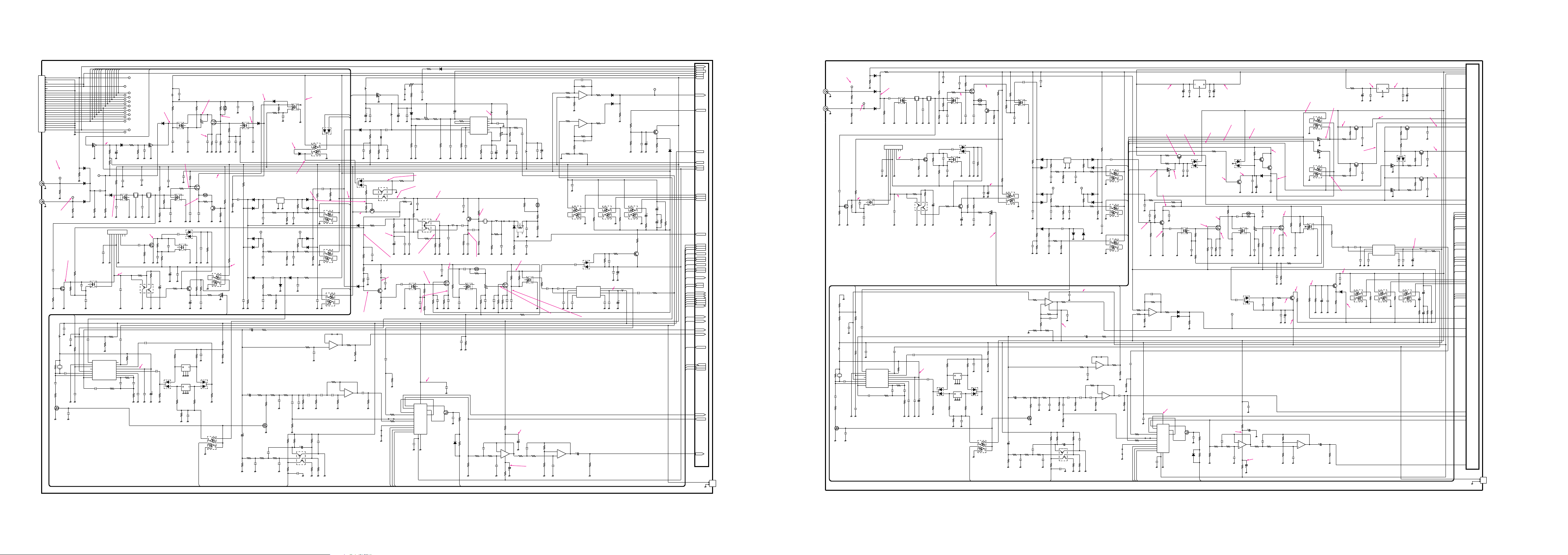
XP4312
Q402
1
2
34
5
6
1
C482
2SK1829
Q406
XP4601
Q405
1
2
3 4
5
6
1
2
3 4
5
6
0.01
C469
C467 10
0.0056
C466
0.1
C465
0.0022
C464
47k
R477
1k
R475
1.8k
R474
22k
R473
22k
R472
22k
R471
47k
R470
47k
R469
W483
0.1
C468
R479 56k
R478 220
180k
R476
-5V
56k
R486
10k
R485
0.1
C474
680p
C480
100k
R498
47k
R499
0.0022
C479
100k
R489
10k
R488
220p
C476
270k
R487
470p
C475
NJM2058M
IC451B
5
6
7
NJM2058M
IC451A
4
11
3
2
1
10
C485
10
C484
100
R497
100
R496
1
C481
22k
R495
AFM
BFOM
BFOM
-
5V
-
5V
AFM
DRES
AFIS
AFIM
PDAT
PCK
from PLL
unit J601
DRES
AFIS
AFIM
PDAT
PCK
J501
2
1
AFSM
AFTM
5V
5V
AFFM
47k
R490
220k
R491
1SS355
D491
0.1
C486
2SJ364
Q407
BU4053BCFV
IC452
78
16
4
Z
15
Y
14
X
9
C
10
B
11
A
6
INH
3
Z1
5
Z0
1
Y1
2
Y0
13
X1
12
X0
0.1
C473
W484
W264
W201
R481 10k
R484 3.3k
220k
R482
470k
R458
0.01
C472
0.22
C483
0.01
C478
10k
R465
22k
R466
NJM2058M
IC451D
12
13
14
47k
R468
3.9k
R467
0.1
C463
0.01
C462
1
C459
C477 0.033
22k
R414
4.7k
R456
10k
R492
22k
R409
4.7k
R464
0.1
C461
0.033
C460
47k
R407
DAN222
D402
DAN222
D401
CFWS455E
FI312
0.1
C413
22k
R405
22k
R408
22k
R406
CFWS455HT
FI311
C410 22
3.3k
R404
100k
R421
150k
R403
390k
R420
0.1
C416
C409 0.1
C408 0.1
C407 220p
220p
C406
0.01
C417
2SK1829
Q404
TA31136FN (D)
IC401
16
MIXIN
15
GND
14
N-REC
13
N-DET
12
RSSI
11
IFOUT
10
QUAD
9
AFOUT8FILIN
7
FILOUT
6
DEC
5
IFIN
4
VCC
3
MIXOUT
2
OSCOUT
1
OSCIN
3.3k
R410
0.01
C414
R401 3.3k
CDBM455C24
X401
330k
R402
0.01
C405
0.22
C403
100p
C402
0.01
C404
0.1
C425
0.01
C110
100µH
L401
0.1
C401
4.7k
R419
100k
R105
22k
R412
22k
R411
0.1
C412
1.5k
R413
0.01
C421
0.1
C411
0.0022
C117
150
R113
4.7
C116
9V
9V
OUTM
BFOM
5V
4.7k
R457
1
C457
DTC144EU
Q106
3.3k
R417
10k
R418
1k
R166
0.01
C159
0.01
C158
4.7k
R164
10k
R463
2.2k
R462
W461
4.7k
R167
0.01
C157
NJM2058M
IC451C
10
9
8
470k
R459
0.22
C458
XP4312
Q153
1
2
34
5
6
4.7k
R163
R355 120
2.2k
R344
470
R353
C354 0.0047
0.01
C355
0.01
C352
47k
R372
9V
RSIM
RSIM
BFOM
5V
RSIM
5V
BFOM
OUTM
CENM
9V
RSIM
AGCM
5V
BFOM
9V
RSIM
AGCM
5V
-
5V
BFOM
AFIS
AFIM
R363 120
C359 0.0047
0.01
5V
5V
9V
C353
C360 0.01
C358 0.01
0.01
C356
R375 100k
15k
R374
R361 47k
R362 470
0.1
C361
0.01
C369
10
C370
0.1
C368
0.1
C367
0.1
C366
12TP
DSSW
12PV
1FOR
CTCM
CENM
NSQM
12ST
12PS
12DS
12UL
OUTM
12TP
DSSW
12PV
1FOR
12ST
12PS
CTCM
CENM
NSQM
12DS
12UL
OUTM
RXS
TXS
SQLM
AF2M
AF1M
OPB1
NBSM
TCWM
WNCM
1FTM
1F2M
1F1M
-
5V
MODO
MODO
RXS
TXS
SQLM
AF2M
AF1M
OPB1
NBSM
TCWM
WNCM
1FTM
1F2M
1F1M
MODO
2SC4116
Q305
0.01
C371
100
R369
1k
R317
120p
C309
0.01
C364
100p
C365
22k
R316
TA4101F
IC351
8
COLECT
7
GND
6
BASE
5
BASE4BASE
3
OSCIN
2
VCC
1
IFOUT
100µH
L355
10
C312
0.1
C311
100p
C310
100k
R315
1SS375
D303
27p
C260
100
R368
100
R364
8.2k
R365
LS-480
L353
LS-476
L354
100
R356
0.01
C357
NTCCM16084BH
NTCCM16084BH
R358
470k
R262
47k
R359
3SK131
Q352
RV-110
R360
0.001
C261
180p
C258
2.2k
R261
22k
R260
27k
R259
1.5k
R257
2.2
C251
100
R341
2.7k
R346
1k
R340
10
R345
0.1
C345
LS-479
L352
2SC4116
Q350
0.0047
C344
0.0047
C342
0.0047
C340
2.7k
R371
0.01
C372
3SK131
Q351
0.01
C254
0.01
C252
100p
C253
3.3k
R256
220
R255
22k
R254
1FTM
1F2M
CP152
820
R161
0.01
C161
6.8k
R168
10p
C160
MA77
D162
MA77
D161
0.01
C156
MA77
D352
XP4312
Q152
1
2
34
5
6
MA77
D158
MA77
D157
R162 100
4.7k
R160
CP151
1.5k
R158
47
R9V9V9V
R114
0.01
C153
MA77
D159
MA77
D156
MA77
D155
UFR9
1k
R165
100
R159
XP4312
Q107
1
2
34
5
6
C119 0.01
C118 10
C121 56p
0.001
C102
XP4601
Q103
123
456
LS-513
L102
47k
R110
2.2k
R109
47k
R108
100
R103
1SS375
D101
C103 0.01
0.015
C113
2SC4116
Q105
2SK882
Q101
R112 1k
R111 5.6k
R104 470k
4.7k
R102
100k
R101
10
C115
C106 470p
120p
C104
C108 56p
0.01
C101
LS-513
L103
LA1150N
IC101
76185432
2SK882
Q102
100
R107
R106 4.7k
2p
C107
UFR9
CP53
CP52
J52
J51
VMAIN
UMAIN
0.01
C51
0.01
C53
CP51
MA77
D54
MA77
D53
MA77
D52
MA77
D51
2.2k
R56
2.2k
R55
2.2k
R54
47k
R53
R52 47k
R51 47k
0.0047
C56
LS-480
L51
LS-480
L52
0.01
C58
0.01
C55
0.01
C52
0.01
C61
FL-211
FI51B
FL-211
FI51A
3SK131
Q51
0.1
C57
C54 4p
R63 120
NTCCM16084LH
R62
470k
R61
R60 22
R59 3.9k
10k
R58
100k
R57
9V
9V
R9V
-
5V
R9V
-
5V
R9V
AGCM
0.01
C60
5.6k
R67
1.5k
R152
0.01
C62
0.01
C151
0.01
C59
MA77
D152
MA77
D151
100
R153
4.7k
R151
MA77
D55
2SC4116
Q52
LS-476
L53
T9V
T9V
2.2k
R68
100
R66
10k
R65
10k
R64
1F1M
4.7k
R169
DAN222
D205
820
R155
MA77
D252
0.01
C162
0.01
C152
FL-128
FI151
43
21
XP4312
Q151
1
2
34
5
6
MA77
D154
MA77
D153
4.7k
R157
100
R156
4.7k
R154
UFR9
-
5V
AGCM
R9V
9V
T9V
470
R251
470
R252
47k
R271
10k
R268
4.7k
R269
47k
R270
C266 0.01
100µ
L251
FMW1
Q253
2
15
4
3
1k
R253
10µH
L253
10µH
L252
R265
LS-256
L255
CR-451
X251
0.047
C262
100p
C259
0.1
C257
330p
C255
4.7k
R267
27k
R266
10k
R264
22k
R258
12µH
L254
D253 1SV217
2SC4116
Q254
RSIM
BFOM
-
5V
9V
AGCM
R9V
0.1
C314
330k
R311
10k
R310
XP4312
Q304
1
2
34
5
6
XP4312
Q303
1
2345
6
XP4601
Q271
2SA1586
Q252
XP4312
Q302
1
2
3
4
5
6
AGRM
AGFM
AGSM
-
5V
AGSM
AGFM
AGRM
R9V
2.2
C308
10
C307
22
C306
R314 680k
R313 4.7k
22k
R312
RFGM
5V
RFGM
ALC
MA728
D302
2SC4116
Q301
0.01
C304
10
C305
470
R309
ALC
MA728
D305
2.7k
R307
330k
R1879
330k
R1887
10k
R1888
470k
R1880
4.7k
R1891
470
R1882
1.2M
R304
0.001
C1876
NJM2058
IC1804C
10
9
8
220k
R1881
4.7k
R308
1
C206
0.01C212
0.1
C218
1k
R215
NJM1496V
IC201
14
V
-
13
NC
12
VO
-
11
NC
10
VC
-
9
NC
8
VC+
7
NC
6
VO+
5
BIAS
4
VS
-
3
VCS
2
VCS
1
VS+
1.5k
R209
22µH
L203
1k
R216
100k
R221
100k
R220
1k
R222
2.7k
R213
330
R208
0.1
C213
10
C214
10
C211
0.1
C210
0.1
C219
0.1
C209
L204 100µH
ALC
8.2k
R218
1.5k
R210
MA77
D202
2.7k
R217
0.0047
C217
1SS355
D201
C203 2.2
C204 0.1
0.01
C216
1k
R206
0.01
C215
1k
R212
1k
R211
15k
R207
15k
R205
470p
C208
470p
C207
0.1
C202
10
C201
22µH
L202
1F2M
1F1M
DAN222
D206
1SS355
D204
XP4312
Q251
1
2
34
5
6
MA77
D203
ALC
33k
R8
C6 0.0047
LS-476
L3
C5 0.01
0.01
C10
0.01
C8
NTCCM16084LH
R5
3SK131
Q1
4.7k
R10
220
R9
R7 3.3k
R6 39
22k
R4
C7 0.22
MA77
D2
RV-148
R3
22k
R22
DTC114EU
Q22
0.01
C2
C22 0.47
47k
R23
1SS355
D21
LS-479
L2
C4 0.01
0.01
C3
100
R2
2.2k
R1
MA77
D1
GND
GND
-
5V
12PS
1FOR
12PV
PCK
PDAT
OPB1
GND
IFS
12ST
12DS
12UL
22k
R24
2.2k
R21
3.3
C21
DTC144EU
Q21
DRES
12TP
IFM
14V
14V
TXS
RXS
from
option
unit
UX-910
from PA
unit J501
from PA
unit J1
GND
GND
J2
25
24
23
22
21
20
19
18
17
16
15
14
13
12
11
10
9
8
7
6
5
4
3
2
1
T9V
14V
IFS
IFM
-
5V
0.01
C1
100µH
L1
TCWM
1k
R203
R219 470
D207 1SS355
0.1
C205
RV-150
R202
DTC144EU
Q201
100µH
L201
KDS
IFS
SSBI
SSBI
9V
14V
T9V
2.2M
R302
MA728
D304
470
R306
C313 0.001
NJM2058
IC1804D
12
13
+
+
-
-
+
-
+
-
+
-
+
-
R305 4.7M
4.7M
R303
KDS
SMLM
IFS
MAIN
UNIT
(1)
9V
9V
9V
14V
T9V
SSBI
KDS
SMLM
IFS
14V
SSBI
T9V
9V
CP853
MAIN
UNIT (2)
KDS
NBSM
NSQM
WNCM
CTCM
DSSW
SQLM
AF1M
AF2M
RSIM
TX:0.077
RX:8.73
TX:0
RX:5.25
TX:0
RX:8.22
1.850
8.22
4.92
4.98
8.48
MESUREMENT CONDITIONS
DIGITAL MULTIMETER
Unit:Volt
-
4.40
7.22
TX:5.17
RX:0
TX:8.41
RX:0
TX:0.262
RX:0
TX:0
RX:0.840
TX:0
RX:7.94
TX:0
RX:0.846
TX:1.936
RX:0
TX:3.40
RX:0
TX:0
RX:7.94
MAIN-FM:8.96
other :0
9.14
TX:0
RX:9.25
RX(MAIN-FM) :9.21
RX(except MAIN-FM):8.44
TX :0
TX(FM):9.06
other :0
TX(FM):6.36
other :0
RX(except MAIN-FM):9.13
other :0
RX(except MAIN-FM):7.95
other :0
RX(except MAIN-FM):7.93
other :0
RX(except MAIN-FM):1.154
other :0
RX(except MAIN-FM):5.31
other :0
RX(except MAIN-FM):4.66
other :0
RX(except MAIN-FM):1.151
other :0
TX(FM):8.98
other :0
TX(FM) :6.55
TX(except FM):0.602
RX :0
TX(FM) :9.20
TX(except FM) :0.545
RX(MAIN-FM) :0.212
RX(except MAIN-FM):0.305
TX:0
RX:9.24
8.98
430MHz MAIN-RX:4.41
430MHz TX :5.83
other :0
144MHz MAIN-RX:4.41
144MHz TX :5.83
other :0
TX(FM):0.297
other :0
TX(FM):0.828
other :0
4.90
RX(except MAIN-FM):1.157
other :0
RX(except MAIN-FM):1.157
other :0
TX(FM):4.82
other :0
TX(FM):4.20
other :0
12-6 MAIN UNIT (2)
0.01
C963
2SK1829
Q952
47k
R958
0.1
C961
XP4312
Q951
1
2
34
5
6
1
C1032
C1020 10
XP4601
Q953
1
2
3 4
5
6
0.01
C1018
1.8k
R1023
0.0056
C1015
0.1
C1014
0.0022
C1013
R1026 47k
1k
R1024
22k
R1022
22k
R1021
22k
R1020
47k
R1019
47k
R1029
AFFS
AFTS
AFSS
W1003
10k
R1030
W1004
3.3k
R1033
0.1
C1019
R1028 56k
R1027 220
R1025 180k
0.1
C1022
47k
R1045
220k
R1049
1SS355
D1041
C1045 0.1
2SJ364
Q1002
470p
C1024
220p
C1025
270k
R1036
56k
R1035
BU4053BCFV
IC1002
7.8
.
16
.
4
Z
15
Y
14
X
9
C
10
B
11
A
6
INH
3
Z1
5
Z0
1
Y1
2
Y0
13
X1
12
X0
0.1
C1023
10k
R1034
-
5V
1
C1030
AFS
AFRP
680p
C1029
47k
R1047
100k
R1046
0.0022
C1028
100k
R1038
10k
R1037
NJM2058M
IC1001B
5
6
7
100
R1043
10
C1017
NJM2058M
IC1001A
4
11
3
2
1
100
R1044
10
C1016
22k
R1048
AFIS
AFIS
AFS
MAIN UNIT (3)
AFRP
AFIM
AFRP
AFIM
J1051
from PLL
unit J701
2
1
0.1
C1036
220k
R1040
10k
R1013
2.2k
R1012
470k
R1039
0.01
C1034
0.01
C1027
0.22
C1033
22k
R1017
47k
R1018
NJM2058M
IC1001D
12
13
14
NJM2058M
IC1001C
10
9
8
3.9k
R1016
470k
R1009
0.1
C1012
0.01
C1011
0.22
C1007
1
C1008
22k
R964
2SK1829
Q1001
4.7k
R1008
10k
R968
4.7k
R1042
C1026 0.033
10k
R1014
R1015 10k
0.1
C1010
C1009 0.033
DAN222
D952
DAN222
D951
0.1
C960
22k
R966
22k
R965
CFWS455E
FI512
22k
R960
22k
R956
22k
R959
22k
R957
1.5k
R955
CFWS455HT
FI511
22
C958
0.1
C959
C957 0.1
C956 0.1
220p
C955
3.3k
R954
150k
R953
3.3k
R961
0.01
C962
TA31136FN (D)
IC951
16
MIXIN
15
GND
14
N-REC
13
N-DET
12
RSSI
11
IFOUT
10
QUAD
9
AFOUT8FILIN
7
FILOUT
6
DEC
5
IFIN
4
VCC
3
MIXOUT
2
OSCOUT
1
OSCIN
CDBM455C24
X951
R951 3.3k
100p
C951
220p
C954
0.01
C953
0.22
C952
330k
R952
0.1
C966
0.01
C950
4.7k
R969
4.7k
R969
390k
R970
100k
R971
0.01
C964
BFOS
0.1
C973
100µH
L951
0.1
C965
0.001
C1879
0.1
C1878
470
R1886
330k
R1883
47k
R1890
330k
R1889
3.3k
R967
NJM2058M
IC1804A
4
11
3
2
1
220k
R1885
R1884 470k
2.2M
R902
1
C1031
1.2M
R927
W1011
4.7k
R1031
4.7M
R904
4.7M
R903
NJM2058M
IC1804B
5
6
7
-
5V
BFOS
SMLS
9V
9V
5V
CP854
MA728
D905
MA728
D904
470
R905
4.7k
R1892
120p
C904
R909 2.7k
10
C907
R910 4.7k
1k
R908
100k
R906
C908 10
0.1
C906
100p
C905
9V
5V
-
5V
BFOS
C909 0.01
470
R911
DSSW
DSSW
NSQS
RFGS
SMLS
NSQS
RFGS
OUTS
C912 2.2
5V
BFOS9V-
5V
-
5V
-
5V
BFOS
R915 4.7k
R916 680k
R914 22k
22
C910
SQLS
AF2S
AF1S
NBSS
CTCS
CENS
WNCS
WNCS
1FTS
1F2S
1F1S
9V
AGCS
AGSS
AGFS
AGRS
SQLS
AF2S
AF1S
CTCS
CENS
NBSS
1FTS
1F2S
1F1S
AGSS
AGFS
AGRS
0.01
C868
10
C911
100
R868
100µH
L854
MA728
D903
2SC4116
Q902
0.01
C866
0.01
C861
0.1
C913
0.1
C865
0.1
C864
0.1
C863
100p
C862
R913 330k
R912 10k
XP4312
Q905
1
2345
6
XP4312
Q904
1
2345
6
XP4312
Q903
1
2345
6
TA4101F
IC851
8
COLECT
7
GND
6
BASE
5
BASE
4
BASE
3
OSCIN
2
VCC
1
IFOUT
10
C867
2SC4116
Q901
0.0047
C871
120
R858
0.01
C859
C870 0.01
0.01
C856
0.01
C857
100k
R874
15k
R873
470
R869
R863 47k
22k
R907
1SS375
D902
R854 120
0.01
C854
470
R852
C853 0.0047
0.01
C851
0.01
C855
47k
R871
AGCS
0.1
-
5V
C1877
0.001
C903
0.01
C762
XP4312
Q753
1
2
34
5
6
4.7k
R769
C763
0.0047
3.3k
R766
1k
R765
4.7k
R767
0.01
C759
0.01
C758
C711 56p
R707 4.7k
2SK882
Q702
0.0015
C716
0.01
C713
100
R708
100k
R706
2p
C710
LS-513
L704
4.7
C719
10
C718
R711
2.2k
47k
R710
XP4601
Q703
123
456
0.0022
C720
150
R715
R714 1k
R713 5.6k
47k
R712
2SC4116
Q705
CP751
1.5k
R763
1.5k
R758
DTC144EU
Q706
47
R716
0.01
C721
10p
C760
0.01
C754
R760 4.7k
MA77
D759
MA77
D756
MA77
D755
1k
R764
100
R759
XP4312
Q707
1
2
3 4
5
6
10
C722
1FTS
1F2S
CP752
C843
0.0047
0.1
C842
4.7k
R841
10
R844
820
R761
MA77
D761
MA77
D762
0.01
C756
XP4312
Q752
1
2
34
5
6
MA77
D758
MA77
D757
R762 100
2.7k
R845
R846 470
100
R843
100
R855
LS-479
L851
2.2k
R842
2SC4116
Q850
0.0047
C841
0.0047
C840
2.7k
R875
3SK131
Q851
0.1
C819
2SC4116
Q817
0.47
C827
RV-110
R857
100
R859
8.2k
R851
LS-476
L853
LS-480
L852
0.01
C872
47k
R862
0.01
C869
NTCCM16084BH
R861
3SK131
Q852
100
R864
DTC144EU
Q814
RXS
TXS
430S
430M
144S
144M
UT9V
T9V
R9V
RXS
TXS
430S
144S
430M
144M
UT9V
R9V
T9V
47k
R821
1k
R820
0.1
C825
UR9V
VR9V
VUT9
VT9V
VR9V
UR9V
VUT9
VT9V
2SA1588
Q813
2SA1588
Q815
47k
R819
1k
R818
0.1
C824
0.1
C823
2SA1588
Q811
1k
R816
DTC144EU
Q812
2SA1586
Q810
2SA1586
Q807
DAP222
D806
47k
R815
47k
R814
1k
R813
47k
R812
1k
R811
0.1
C822
0.1
C821
2SD1801
Q804
DA221
D807
2SC4116
Q816
1k
R824
XP4312
Q809
1
2
34
5
6
DTC144EU
Q808
DTC144EU
Q806
1SS355
D805
10k
R822
R807 10
DA221
D804
2SD1664
Q801
R808 2.2k
0.1
C818
0.1
C817
DTC144EU
Q831
1F1S
430S
144S
144M
430M
RXS
TXS
0.01
C753
820
R755
0.01
C752
XP4312
Q751
1
2
34
5
6
MA77
D754
MA77
D753
4.7k
R757
100
R756
1.5k
R752
0.01
C751
R754
4.7k
MA77
D752
MA77
D751
FL-129
FI751
43
21
100
R753
4.7k
R751
C723
56p
LS-513
L703
2SK882
Q701
120p
C732
R705 470k
100
R704
R703 4.7k
100k
R702
1SS375
D701
C709 470p
0.01
C708
0.001
C706
0.01
C701
LA1150N
IC701
76185432
18k
R655
CP652
9V
CP651
J652
J651
VSUB
USUB
IFS
from PA
unit J510
from PA
unit J30
0.01
C651
MA77
D651
MA77
D653
MA77
D652
2.2k
R654
47k
R653
47k
R652
47k
R651
0.0047
C656
3.3k
R659
LS-480
L651
LS-480
L652
0.01
C658
0.01
C655
0.01
C661
FL-212
FI651B
FL-212
FI651A
3SK131
Q651
0.1C657
5pC654
120
R663
NTCCM16083NH
R662
470k
R661
22
R660
10kR658
100k
R657
AGCS
5.6kR666
0.01
C660
0.01
C659
0.01
C662
2SC4116
Q652
LS-476
L653
100R667
10k
R665
10k
R664
0.1
C802
0.1
C826
470
C801
4.7
C828
10
IFS
14V
14V 9V
9V
C803
BA09T
IC801
XP4312
Q805
1
2
34
5
6
0.1
C813
6.8
R805
10
C814
100
C816
0.1
C815
TA7805S
IC803
IFS
9V
5V
14V
-
5V
IFS
5V
MAIN
UNIT
(1)
-
5V
14V
9V
CENS
NBSS
NSQS
RSIS
WNCS
CTCS
DSSW
SQLS
AF1S
AF2S
144MHz SUB-RX:4.61
other :0
430MHz SUB-RX:4.55
other :0
144MHz SUB-RX:3.85
430MHz SUB-RX:3.78
0.829
6.97
8.16
-
5.00
13.46
8.70
TX:13.3
RX:13.0
TX:5.0
RX:0
TX:0
RX:9.86
5.32
1.161
7.96
-
5.00
-
4.94
7.96
TX:13.30
RX:13.46
TX:9.24
RX:0
TX:10.5
RX:0
TX:0
RX:0.694
2.06
2.57
9.08
4.90
1.927
MESUREMENT CONDITIONS
DIGITALMULTIMETER
Unit:Volt
1.156
1.123
4.69
1.135
TX:0
RX:9.23
430MHz MAIN:4.79
other :0
144MHz SUB:4.92
other :0
144MHz MAIN:4.78
other :0
430MHz TX:0.106
other :9.02
144MHz:9.09
144MHz:0.072
other :0.182
430MHz TX:9.09
430MHz RX:0.068
other :0.118
430MHz TX:9.15
other :0
144MHz TX:9.15
other :0
144MHz TX:0
other :9.05
MAIN- TX:9.11
MAIN-RX:0
9.13
12.41 4.99
430MHz SUB:4.90
other :0
9.15
4.92
4.97
8.46
-
4.38
9.08
SUB NB ON:4.95
8.32
1.824
8.17
12-7 MAIN UNIT (3)
12 - 6
 Loading...