


®
IBM PowerPC® 970MP RISC Microprocessor
Application Note
®
PowerPC
(Includes Differences for 970FX to 970MP)
970MP Differences
Version: 1.0
Preliminary
November 15, 2006

Application Note
(Includes Differences for 970FX to 970MP)
IBM PowerPC® 970MP RISC Microprocessor Preliminary
Copyright and Disclaimer
© Copyright International Business Machines Corporation 2004, 2005, 2006
All Rights Reserved
Printed in the United States of America November 2006
The following are trademarks of International Business Machines Corporation in the United States, or other countries, or
both.
IBM IBM Logo
PowerPC PowerPC Logo
PowerPC 970FX PowerPC Architecture
PowerPC 970MP PowerPC 970
Other company, product and service names may be trademarks or service marks of others.
All information contained in this document is subject to change without notice. The products described in this document
are NOT intended for use in implantation or other life support, space, nuclear, or military applications where malfunction
may result in injury or death to persons. The information contained in this document does not affect or change IBM
product specifications or warranties. Nothing in this document shall operate as an express or implied license or indemnity
under the intellectual property rights of IBM or third parties. All information contained in this document was obtained in
specific environments, and is presented as an illustration. The results obtained in other operating environments may vary.
While the information contained herein is believed to be accurate, such information is advance, and should not be relied
upon for accuracy or completeness, and no representations or warranties of accuracy or completeness are made.
Note: This document contains information on products in the design, sampling and/or initial production phases
of development. This information is subject to change without notice. Verify with your IBM field applications
engineer that you have the latest version of this document before finalizing a design.
THE INFORMATION CONTAINED IN THIS DOCUMENT IS PROVIDED ON AN "AS IS" BASIS. In no event will IBM be
liable for damages arising directly or indirectly from any use of the information contained in this document.
IBM Systems and Technology Group
2070 Route 52, Bldg. 330
Hopewell Junction, NY 12533-6351
The IBM home page can be found at www.ibm.com
The IBM Microelectronics home page
can be found at www-3.ibm.com/chips/
Title_970FX-MP_Differences.fm.1.0
November 15, 2006 -Preliminary
Page 2 of 25
Title_970FX-MP_Differences.fm.1.0
November 15, 2006

Application Note
(Includes Differences for 970FX to 970MP)
Preliminary IBM PowerPC® 970MP RISC Microprocessor
1. Abstract ....................................................................................................................... 9
2. Overview ...................................................................................................................... 9
3. Processor Version Register (PVR) ............................................................................ 9
4. General Parameters .................................................................................................. 10
5. Design Enhancements for PowerPC 970MP .......................................................... 10
5.1 Dual Core Design ............................................................................................................................ 10
5.1.1 1MB L2 Cache per Core ........................................................................................................ 12
5.2 Processor Interconnect Bus ............................................................................................................ 13
5.2.1 SCOM control and status registers ........................................................................................ 13
5.2.2 Test Modes ............................................................................................................................ 13
5.2.2.1 Transmitter Pseudo-Random Data Test (RDT) .............................................................. 13
5.2.2.2 Transmitter Electrical Shorts Test (EST) ........................................................................ 13
5.2.2.3 Receiver Electrical Shorts Test (REST) ......................................................................... 14
5.2.2.4 Receiver Random Data Self Test ................................................................................... 15
5.2.3 Bus Configuration .................................................................................................................. 15
5.3 PowerTuning ................................................................................................................................... 17
5.3.1 Power Modes ......................................................................................................................... 17
5.3.2 Time Base and Decrementer ................................................................................................. 18
2
5.4 I
C Bus Interface ............................................................................................................................. 18
5.4.1 Clock Dithering (New feature for 970FX DD3.0, enhanced in 970MP) ................................. 18
5.4.2 Programmable Delays for Power Saving Mode Transitions .................................................. 19
5.5 Additional Dynamic Power Management ........................................................................................ 19
5.6 More Precise Kelvin Circuitry .......................................................................................................... 19
7. Timings ...................................................................................................................... 20
8. Package ..................................................................................................................... 20
8.1 Design Considerations for a 970MP Thermal Solution ................................................................... 20
8.1.1 Die Size ................................................................................................................................. 20
8.1.2 Capacitor Position ................................................................................................................. 21
8.2 Description of Signal Changes ........................................................................................................ 21
8.3 PowerPC 970MP Microprocessor Package Dimensions ................................................................ 22
Revision Log ................................................................................................................ 25
AppNote_970FX-MP_Differences_TOC.fm.1.0
November 15, 2006
Page 3 of 25

Application Note
(Includes Differences for 970FX to 970MP)
IBM PowerPC® 970MP RISC Microprocessor Preliminary
Page 4 of 25
AppNote_970FX-MP_Differences_TOC.fm.1.0
November 15, 2006

Application Note
(Includes Differences for 970FX to 970MP)
Preliminary IBM PowerPC® 970MP RISC Microprocessor
Figure 5-1. Dual Cores sharing processor interface ................................................................................. 11
Figure 5-2. 970MP Power Modes ............................................................................................................. 17
Figure 8-1. PowerPC 970MP Mechanical Package (Side and Top View) ................................................ 23
Figure 8-2. PowerPC 970MP Bottom Surface of CBGA Package (Bottom View) .................................... 24
AppNote_970FX-MP_Differences_LOF.fm.1.0
November 15, 2006
Page 5 of 25

Application Note
(Includes Differences for 970FX to 970MP)
IBM PowerPC® 970MP RISC Microprocessor Preliminary
Page 6 of 25
AppNote_970FX-MP_Differences_LOF.fm.1.0
November 15, 2006

Application Note
(Includes Differences for 970FX to 970MP)
Preliminary IBM PowerPC® 970MP RISC Microprocessor
Table 3-1. PowerPC 970FX and 970MP Processor Version Registers (PVR) .......................................... 9
Table 4-1. General Parameters of the PowerPC 970FX and 970MP ...................................................... 10
Table 5-1. PowerPC 970MP Programmable Delay Parameters ............................................................. 16
Table 5-2. Power Mode States ................................................................................................................ 18
Table 5-3. PowerPC 970MP Latency of Deep Nap to Run Transition (Full Frequency Cycles) ............. 19
Table 8-1. PowerPC 970FX, and 970MP Die Size and Dimensions ....................................................... 20
Table 8-2. 970FX Pins Duplicated for each 970MP Processing Unit ...................................................... 21
Table 8-3. New 970MP Pins .................................................................................................................... 21
Table 8-4. Deleted 970FX Pins - not found on 970MP ............................................................................ 22
AppNote_970FX-MP_Differences_LOT.fm.1.0
November 15, 2006
Page 7 of 25

Application Note
(Includes Differences for 970FX to 970MP)
IBM PowerPC® 970MP RISC Microprocessor Preliminary
Page 8 of 25
AppNote_970FX-MP_Differences_LOT.fm.1.0
November 15, 2006

Application Note
(Includes Differences for 970FX to 970MP)
Preliminary IBM PowerPC® 970MP RISC Microprocessor
1. Abstract
This preliminary application note describes the differences between the PowerPC® 970FX microprocessor
and PowerPC 970MP microprocessor. The primary objective of the PowerPC 970FX remap to the 970MP is
to achieve a high frequency dual core processor. The design changes include a 1MB L2 cache per core,
support for higher bus speeds, power management improvements, and errata fixes.
2. Overview
The IBM 970MP RISC Microprocessor is a dual-core, 64-bit implementation of the IBM PowerPC® family of
reduced instruction set computer (RISC) microprocessors that are based on the PowerPC Architecture. This
dual microprocessor, also called the 970MP, includes a Vector/SIMD facility in each core which supports
high-bandwidth data processing and compute-intensive operations. The 970MP is designed to support
multiple system organizations, including desktop and low-end server applications, up through 4-way SMP
configurations.
The differences between the PowerPC 970FX and 970MP designs are described in the following sections:
• Process Version Register
• General Parameters
• Design Enhancements
• System Design Information
• Timings
•Package
3. Processor Version Register (PVR)
The PowerPC 970FX and 970MP have the following PVR values for the respective design revision levels.
Table 3-1. PowerPC 970FX and 970MP Processor Version Registers (PVR)
Design Revision Level 970FX PVR 970MP PVR
DD1.0 0x00391100 0x00440100
DD1.1 — 0x00440101
DD2.0 0x003C0200 —
DD2.1 0x003C0201 —
DD3.0 0x003C0300 —
DD3.1 0x003C0301 —
AppNote_970FX-MP_Differences_Body.fm.1.0
November 15, 2006
1. Abstract
Page 9 of 25

Application Note
(Includes Differences for 970FX to 970MP)
IBM PowerPC® 970MP RISC Microprocessor Preliminary
4. General Parameters
Table 4-1 provides a summary of the general parameters for the PowerPC 970FX and 970MP.
Table 4-1. General Parameters of the PowerPC 970FX and 970MP
Item 970FX Description 970MP Description
Die Size 66.2 sq. mm 153.8 sq. mm
Die Dimensions 7.07mm x 9.36mm 13.225 mm x 11.629 mm
Transistor Count 52 million 183 Million
Logic Design Static with some dynamic logic Static with some dynamic logic
Package
576-pin Ceramic ball grid array (CBGA)
25x25mm (1.0mm pitch)
575-pin Ceramic ball grid array (CBGA)
25x25mm (1.0mm pitch)
5. Design Enhancements for PowerPC 970MP
To create a dual core with improved power savings features, there were several enhancements made to the
PowerPC 970MP design.
This section describes the design enhancements to the 970MP.
5.1 Dual Core Design
The 970MP chip consists of two processing units (PUs), each containing an execution core with L1 caches, a
storage subsystem including L2 cache, and pervasive functions. In addition, a small amount of common logic
that is outside either PU is included to interface each PU to the single bus interface.
The two cores function as would two cores on separate chips for the most part. For example, they maintain
memory coherence via the bridge chip, they are able to Doze independently, and they have private access to
most processor resources including the L2. Also, like processors on separate chips, they scale frequency,
using the power tuning facility, together.
Sharing the same chip constrains the behavior of the two cores in several ways. First, the two PUs have
separate voltage planes for power, but the core voltages will always need to be within the delta specified in
the IBM PowerPC 970MP RISC Microprocessor Datasheet when the two processors are running. Also, the
core frequencies will always be the same. This would be true for two separate cores except for the Deep Nap
case, where one of two separate processors could reduce frequency to 1/64, while the other ran at functional
speed. The two 970MP cores must go into and come out of Deep Nap together.
The other difference between having dual cores on a single chip, versus two separate chips, is that they
share a single PI (processor interconnect) interface to the bridge chip. This requires that the interface
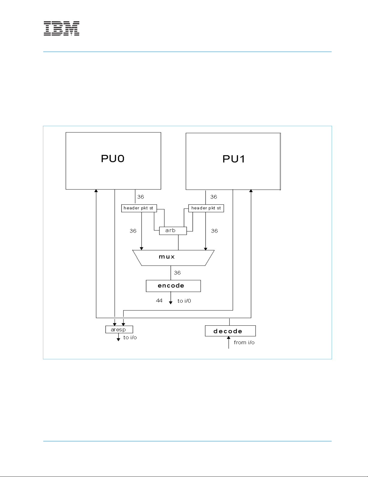
between the BIU and the PI logic be enhanced with buffers and muxes to support the sharing of the PI interface between the two cores. Figure 5-1 on page 11 shows the relationship among the two cores and the
common logic.
For incoming PI data and commands, the output of the PI decoder is passed directly to both processors. For
outgoing PI data and commands, an arbiter and mux are introduced in front of the PI encoder to give one or
the other processor access to the outgoing PI bus at any given time. The arbiter implements a round robin
4. General Parameters
Page 10 of 25
AppNote_970FX-MP_Differences_Body.fm.1.0
November 15, 2006
Application Note
(Includes Differences for 970FX to 970MP)
Preliminary IBM PowerPC® 970MP RISC Microprocessor
scheme, with provisions for adjusting priorities when one core receives repeated serial retries. Logic in the
BIU of each PU is modified to allow the arbiter to hold that PU from sending data to the PI bus when a transaction from the other processor is in progress. The PI bus configuration parameters apply to the single bus,
not to the individual processors, and so this arbiter enforces those parameters, such as the COMPACE
timing, for example. In order to minimize dead time on the bus, header packets for each processor are
queued at the arbiter. Finally, snoop responses from the two processors are combined on chip, and sent as a
single response over the PI bus to the bridge chip, as indicated in the lower left corner of Figure 5-1.
Figure 5-1. Dual Cores sharing processor interface
The additional logic at the PI/BIU interface requires a SNOOPLAT (and SNOOPACC) value that is larger than
for the 970FX, but still within the programmable range. The maximum STATLAT value on 970MP is increased
to 30, and it is expected that the bridge chip will need to similarly be designed for a higher maximum value
than was previously used. Refer to the IBM PowerPC 970MP Design Guidelines for more information.
Intercommunication between the processors on chip occurs in the same way as if they were on separate
chips, via the bridge chip. In particular, on-chip L2 to L2 intervention is not supported.
AppNote_970FX-MP_Differences_Body.fm.1.0
November 15, 2006
5. Design Enhancements for PowerPC 970MP
Page 11 of 25

Application Note
(Includes Differences for 970FX to 970MP)
IBM PowerPC® 970MP RISC Microprocessor Preliminary
5.1.1 1MB L2 Cache per Core
The 970MP L2 cache design doubles the cache array size and capacity from 970FX, with a corresponding
doubling in size of the two copies of the L2 tag arrays. Like the 970FX, it is an 8-way set associative cache of
128 B lines, but now consists of 1024 sets. The latency for L1 misses that hit in the L2 is increased by two
processor cycles in the 970MP, due to the longer path from the core to the larger L2 array. This load-use
penalty for fixed-point unit operands that hit in the 1 MB L2 cache is 14 processor cycles.
5. Design Enhancements for PowerPC 970MP
Page 12 of 25
AppNote_970FX-MP_Differences_Body.fm.1.0
November 15, 2006

Application Note
(Includes Differences for 970FX to 970MP)
Preliminary IBM PowerPC® 970MP RISC Microprocessor
5.2 Processor Interconnect Bus
The 970MP design incorporates an enhanced Processor Interconnect (PI) Interface for its high-speed off-chip
bus. There are a number of changes to the physical interface and support hardware associated with the use
of the enhanced definition from that in the 970FX. These changes include modifications to the driver and
receiver, two new test modes of operation, and additional control and status registers.
5.2.1 SCOM control and status registers
The 970FX contains five 32-bit SCOM registers associated with PI (x’04.6A00’, x’0F.6A01’, x’0F.7A00’,
x’04.6B01’, x’0F.6B00’, and x’0F.7B01’). Three of these are mode registers and two are status registers. See
the IBM PowerPC 970FX RISC Microprocessor User’s Manual for a description of these registers. The
970MP replaces these five SCOM registers with a set of sixteen new SCOM registers (located in the common
domain at address x’08.XXXX’). Eight of these are 16-bit registers for fault isolation and error reporting. One
is a 16-bit command register for specifying a clock delay. Two are 64-bit IAP registers that allow programming
of the IAP pattern. Four are 16-bit mode registers. One is a 16-bit status register. This status register is a
read-only register that can be programmed by bits in a mode register (mode register 2, bit 48:54) to return the
status of different aspects of the PI interface, depending on the mode register values. These registers are
only accessible by the master processing unit. The IBM PowerPC 970MP Microprocessor User’s Manual
describes these registers in detail.
Note in particular the different use of the windage field in the 970MP compared with that in the 970FX. In the
970MP, the windage field is used to add a fixed amount of delay to all bits prior to IAP learning, in order to
avoid an underflow when a guardbanding procedure is performed at the end of the IAP.
5.2.2 Test Modes
Two new test modes are supported for bringup of the PI interface. These are the electrical shorts test (EST)
and the pseudo-random data test (RDT). The following sections describe both the transmitter and receiver
support for these functions.
5.2.2.1 Transmitter Pseudo-Random Data Test (RDT)
One new test feature is the pseudo-random data test mode. This mode uses a built in linear feedback shift
register (LFSR) to create pseudo-random patterns to be transmitted across each enabled channel. The LFSR
register is 12 bits wide and implements the polynomial 1+x
3+x5+x11
, using a seed of all 1 bits. These data
patterns can then be received and compared to expected patterns created in the receiver core. This mode is
described in more detail in the corresponding receiver section. Pseudo-random test mode is enabled by
setting the following combination of I/O SCOM mode register 0 bits: WIAP to ‘1’, RDTMODE to ‘1’ and
ESTMODE to ‘0’. The pseudo-random patterns are created as long as this bit combination is set.
5.2.2.2 Transmitter Electrical Shorts Test (EST)
The second new test feature supports a mode which allows the integrity of the off-chip link to be tested to
verify its electrical integrity - that is, to find opens and shorts between channels. In support of this feature, the
transmitter core can create specific patterns that are then verified in the receiver core. Described below are
the patterns created by the transmitter for this mode. This mode is described in detail in the corresponding
receiver section. In short test mode, the transmitter creates a pattern of 16 consecutive data ‘1’ bits on serial
data channel 0, while all other channels are transmitting ‘0’ bits. After 16 bit times, the next sequential
channel will transmit a data ‘1’ for 16 bit times, while the previously enabled channel and all other channels
AppNote_970FX-MP_Differences_Body.fm.1.0
November 15, 2006
5. Design Enhancements for PowerPC 970MP
Page 13 of 25

Application Note
(Includes Differences for 970FX to 970MP)
IBM PowerPC® 970MP RISC Microprocessor Preliminary
are transmitting ‘0’ bits. This process repeats itself until the 16 consecutive ‘1’ bits have been walked in
sequence across all channels. The electrical shorts test mode is enabled by setting the following I/O SCOM
mode register 0 bits: ESTMODE to ‘1’, WIAP to ‘1’, and RDTMODE to ‘1’. Once enabled the shorts test will
create the sequential patterns across all data channels, and then will stop. However, if any of the values of
the three mode bits that enable this mode are changed, the test will be terminated immediately. Once a test is
complete the SCOM mode bit WIAP must be deasserted and reasserted to start a new test.
The electrical shorts test also has a feature controlled by SCOM mode bit ESTONE. Holding ESTONE at a ‘1’
creates the pattern sequence previously described. Forcing ESTONE to a ‘0’ reverses the values of the
pattern sequence, essentially creating a walking ‘0’ sequence across a field of data 1’s.
5.2.2.3 Receiver Electrical Shorts Test (REST)
The transmitter mode called electrical shorts test, which creates a walking ‘1’ or walking ‘0’ pattern, is
discussed in the transmitter description. For the test to be performed correctly both the transmitter and
receiver within the link must have the same ESTONE value applied. Mismatched ESTONE values results in a
failing test.
The walking pattern appears on the data channels as the walking data value on the channel under test,
surrounded by the opposite data value on all other channels in the data field. The walking data value is held
on a given channel for 16 bit times, after which the data value for that channel is returned to the data value of
the field, and the walking value is applied to the next channel for 16 bit times. The process is continued until
all channels have been tested.
Each channel is independently forced to a ‘1’ while the field is ‘0’. Each time a channel is tested by applying a
data ‘1’ the receiver checks to see that the channel under test, and only the channel under test, observes the
‘1’. If at any time more than one channel is received as a ‘1’, a short between the channel under test and other
channel(s) observing a ‘1’ exists. If any channel under test fails to observe the ‘1’ an error on that channel is
indicated.
The following is the process for performing the shorts test:
• 1. Configure receiver in bypass mode, SCOM mode reg BYPASS=1.
• 2. Force transmitter to send data ‘0’ on all channels if ESTONE=1, or send data ‘1’ on all channels if
ESTONE=0.
• 3. Wait for receiver to be flushing 0’s or 1’s, as appropriate.
• 4. Start receiver SCOM mode reg ESTMODE and RIAP set active.
• 5. Start transmitter SCOM mode reg ESTMODE and WIAP set active.
• 6. Receiver status reports errors if test fails.
Note that the link does not require IAP training before the shorts test is run. However, for the test to be
successful the receiver must be configured in bypass mode which flushes data through the FIFO within the
receiver. This bypass mode is entered by forcing the SCOM mode register BYPASS bit to ‘1’ before the test is
initiated. The receiver initiates the test by observing all received data channels, and samples data on all channels after the leading edge of the first data transition on channel 0 is observed. This creates a sampling
strobe approximately in the center of the 16 bits of data on the channel under test. The checking procedure
within the receiver expects the channel under test to increment from channel 0 through channel 47.
5. Design Enhancements for PowerPC 970MP
Page 14 of 25
AppNote_970FX-MP_Differences_Body.fm.1.0
November 15, 2006

Application Note
(Includes Differences for 970FX to 970MP)
Preliminary IBM PowerPC® 970MP RISC Microprocessor
If the expected results are not observed, an error is flagged in the status register. The DIAG_RDT vector out
of the receiver provides observability of individual channel failures. The status register, bit 1, also indicates
that the shorts test is complete. Completion of the shorts test within a reasonable period of time should be
verified after the test is initiated with SCOM mode reg ESTMODE and WIAP.
5.2.2.4 Receiver Random Data Self Test
Also discussed in the transmitter description is the Pseudo-Random Data Test (RDT). The receiver also has
an LFSR register built into it, that is capable of duplicating the pseudo-random test patterns that were sent
across the link from the transmitter core. Preceding the random pattern across the link is a solid 0 value.
When the random data self test is initiated within the receiver by enabling the SCOM mode reg RDTMODE
and RIAP, the receiver self-test logic monitors the data received, and when a transition from the solid ‘0’ value
to a ‘1’ is observed, the receiver LFSR register begins to generate patterns which are then compared to the
received data. Once initiated, the random data self-test procedure continues until RDTMODE and RIAP are
disabled.
The following is the process for performing a link random data self test:
• 1. Train the receiver.
• 2. Force the transmitter to send data 0’s.
• 3. Wait for the receiver to be flushing 0’s.
• 4. Start receiver SCOM mode reg RDTMODE and RIAP set active.
• 5. Start transmitter SCOM mode reg RDTMODE and WIAP set active (starts the test).
• 6. Receiver status reports errors if the test fails.
If the expected results are not observed on any channel, an error is flagged in the status register. The
DIAG_RDT vector out of the receiver provides observability of any channel which did not contain expected
values for the duration of the test. Unlike the shorts test previously described, the status register will never
indicate completion of the test, as there is no predefined end to the random data sequence.
For status information to remain valid at the termination of a test, the random data self test should be terminated by deasserting RIAP at the receiver prior to deasserting WIAP at the transmitter. However, since there
is no indication that the random data self test ever started within the receiver, WIAP can be deasserted first,
which provokes errors on all receiver channels upon its deassertion. Status and DIAG_RDT should be monitored before deasserting WIAP to verify that there are no failing channels prior to its deassertion.
The LFSR data sent across the link represents data with a rich mix of data transitions that are much more
random than the IAP training pattern, and therefore stress the link alignment beyond the point that it was
stressed during IAP. A link which successfully completes IAP may still suffer from bit errors when random
data is transferred across the link. Random data self test allows the link to be evaluated for proper alignment
before real data is sent across the link.
5.2.3 Bus Configuration
The larger L2 caches, the bus arbiter between the two cores, and the use of the PI receiver design combine
to introduce additional delay in the path between the L2 cache and the bus interface. In particular, the PI
receiver adds one bus beat of delay, and the bus arbiter adds another bus beat of delay on incoming signals.
The bus arbiter adds two bus beats of delay on the outgoing signals. This results in an additional four bus
beats of latency for a snoop response, for example. The programmable delay parameters described in
AppNote_970FX-MP_Differences_Body.fm.1.0
November 15, 2006
5. Design Enhancements for PowerPC 970MP
Page 15 of 25

Application Note
(Includes Differences for 970FX to 970MP)
IBM PowerPC® 970MP RISC Microprocessor Preliminary
Section 11.4 of the 970FX User’s Manual are set to system dependent values during initialization, and must
account for these larger latencies in the 970MP. The range of values that may be specified for each of these
parameters for the 970MP is:
Table 5-1. PowerPC 970MP Programmable Delay Parameters
Parameter Min. Max
COMPACE 2 14
STATLAT 4 30
SNOOPLAT 6 12
SNOOPACC 9 24
In addition, the definitions of STATLAT, SNOOPLAT, and SNOOPACC in 970MP have changed due to additional staging of bus signals internally. Thus, setting a STATLAT value of 24 in the register corresponds to a
delay of 22 bus beats between the last beat of the ADO packet and the first beat of the transfer-handshake
packet. Similarly, a value two larger than the actual bus delay must be programmed into the SNOOPLAT and
SNOOPACC registers on 970MP.
5. Design Enhancements for PowerPC 970MP
Page 16 of 25
AppNote_970FX-MP_Differences_Body.fm.1.0
November 15, 2006

Application Note
(Includes Differences for 970FX to 970MP)
Preliminary IBM PowerPC® 970MP RISC Microprocessor
5.3 PowerTuning
5.3.1 Power Modes
The twelve power states associated with the power tuning engine frequency scaling facility on the 970MP are
indicated by the nodes S1 through S12 in Figure 5-2.
Figure 5-2. 970MP Power Modes
Deep
L1/R1
Doz e
L2/R2
S2
NapRun
S3
Nap
L4
High
Speed
L21/R21
Medium
Speed
Low
Speed
S1
L7/R7
S5
L14/R14
L15/R15
S9
R3 R5
R6
L9/R9
S6 S7
R12R10
R13
L16/R16
S10
R17
R20
S11
R19
S4
L11L8/R8
S8
L18
S12
The state diagram in Figure 5-2 represents two changes for the 970MP design. First, the Deep Nap state can
be reached from the Nap state at any frequency. Second, frequency scaling between full and quarter
frequency can be done directly.
AppNote_970FX-MP_Differences_Body.fm.1.0
November 15, 2006
5. Design Enhancements for PowerPC 970MP
Page 17 of 25

Application Note
(Includes Differences for 970FX to 970MP)
IBM PowerPC® 970MP RISC Microprocessor Preliminary
Table 5-2 describes the twelve power mode states.
Table 5-2. Power Mode States
State Description
S1 Full Run, High Speed
S2 Doze, High Speed
S3 Nap, High Speed
S4 Deep Nap, High
S5 Full Run, Medium Speed
S6 Doze, Medium Speed
S7 Nap, Medium Speed
S8 Deep Nap, Medium
S9 Full Run, Low Speed
S10 Doze, Low Speed
S11 Nap, Low Speed
S12 Deep Nap, Low
5.3.2 Time Base and Decrementer
The time base and decrementer registers will run at a constant frequency, independent of changes to the
processor and bus frequencies. For 970FX, the default operation of these timers is to run at 1/8 the full
processor frequency, even when the processor itself is running at a lower frequency. For 970MP, the default
operation of these timers is to run at 1/16 the full processor frequency, even when the processor itself is
running at a lower frequency. When TBEN is configured to clock these timers (HID0[19] = 1), the timers will
run at the TBEN frequency. In this case, the maximum allowable TBEN frequency is 1/16 the full processor
frequency.
Since the mesh clock frequency can be lowered to 1/64th of the full-speed, the time base/decrementer may
be increased/decreased by more than one at a time. Therefore testing that the decrementer has reached the
value of zero in order to generate an internal interrupt is not sufficient. The logic detects that the counter has
wrapped around. Additionally the time resolution of the counters is limited by the mesh clock frequency.
5.4 I2C Bus Interface
5.4.1 Clock Dithering (New feature for 970FX DD3.0, enhanced in 970MP)
Input current to the processor can change significantly during power tuning frequency transitions. These
current changes must be controlled in order to avoid over and under-voltages that large di/dt might cause due
to inductance in the power distribution network. In DD3.0 of the 970FX, a clock dithering mechanism was
added in the power tuning hardware, to gradually transition between frequencies. The 970MP replaces the
970FX 24-bit dither with a selectable 24- or 48-bit dither pattern.
5. Design Enhancements for PowerPC 970MP
Page 18 of 25
AppNote_970FX-MP_Differences_Body.fm.1.0
November 15, 2006

Application Note
(Includes Differences for 970FX to 970MP)
Preliminary IBM PowerPC® 970MP RISC Microprocessor
The transition from quarter to full frequency is handled in two stages. First, the processor is transitioned from
quarter frequency to half frequency using the quarter to half dither pattern. The processor is paused for 32
cycles at half frequency, and then transitioned to full frequency using the half to full dither pattern. A similar
procedure is used for the full to quarter frequency transition.
5.4.2 Programmable Delays for Power Saving Mode Transitions
The 970MP design introduces a programmable delay when transitioning between power saving modes, to
reduce di/dt in these cases. For example on interrupt, the processor transitions from Deep Nap, through Nap
and Doze, to Run. The latency is a combination of fixed (full frequency) and mesh clock cycles, plus a
programmable delay. The programmable delay, Dp, is controlled by a 6-bit mode ring value. Dp specifies the
number of full frequency cycles of delay from 0 to 63. This delay occurs 6 times during the Deep Nap to Run
transition.
Table 5-3 lists the latency of Deep Nap to Run Transition for the PowerPC 970MP for full, half, and quarter
frequency scaling.
Table 5-3. PowerPC 970MP Latency of Deep Nap to Run Transition (Full Frequency Cycles)
Full Half Quarter
123 + 6*Dp 228 + 6*Dp 438 + 6*Dp
5.5 Additional Dynamic Power Management
To a limited extent the PowerPC 970 design implements dynamic power management (DPM) – the gating of
clocks to idle circuits while in an operational mode. For example, clocks in the pipelined vector processing
units (VPUs) are gated on a stage by stage basis, as instructions flow through the pipeline. The 970FX design
implements additional dynamic power management in the STS, IDU, and RAS units. The 970MP design
implements additional dynamic power management in the ISU, FXU, and FPU units.
Dynamic power management can be disabled as follows. For the VPU, IDU and STS, DPM is disabled by
negating HID0[DPM]. For the ISU, FXU, FPU and pervasive units, DPM is disabled by setting bit 0 in JTAG
register 0x00.0800 to a ‘1’.
5.6 More Precise Kelvin Circuitry
The 970MP implements circuitry that enables more precise Kelvin measurements. This increased precision
allows for better correlation between the Kelvin signals and the actual voltage applied to the transistors.
However, this improved precision in the Kelvin pins also increased their sensitivity. For DD1.0, DD1.01,
DD1.02, the maximum allowable current is 0.9mA. For DD1.1, the maximum allowable current is 2.7mA.
Exceeding these maximum currents may cause permanent damage to the microprocessor. Oscilloscope
probes should provide enough impedance to prevent excess current on these pins. Due to ESD concerns,
this change was reversed back to the 970FX implementation for DD1.03 and DD1.11+. For additional details,
refer to the IBM PowerPC 970MP RISC Microprocessor Datasheet.
AppNote_970FX-MP_Differences_Body.fm.1.0
November 15, 2006
5. Design Enhancements for PowerPC 970MP
Page 19 of 25

Application Note
(Includes Differences for 970FX to 970MP)
IBM PowerPC® 970MP RISC Microprocessor Preliminary
6. System Design Information
The 970MP supports a 24:1 bus ratio for test purposes instead of the 16:1 bus ratio supported in the 970FX.
The BUS_CFG(0:2) pin setting for this 24:1 bus ratio is ‘110’, which is the same setting that was used to
select the 16:1 bus ratio in the 970FX.
Unlike the 970FX, ANALOG_GND is not shorted to GND within the 970MP. Please refer to the IBM PowerPC
970MP RISC Microprocessor Datasheet for the proper filtering recommendation.
7. Timings
Note: Timings are very processor and technology specific. It should not be assumed that timings remain
equivalent between any of the PowerPC microprocessors designs. Timings for each of the IBM PowerPC
microprocessor family of products are located within their specific electrical specification, referred to as the
“Datasheet.” Contact your IBM Sales or technical support group for the PowerPC 970MP RISC Microproces-
sor Datasheet.
8. Package
8.1 Design Considerations for a 970MP Thermal Solution
The 970MP package differs from the 970FX with respect to:
• Die size/dimension
• Position of the capacitors on the die
8.1.1 Die Size
A thermal solution for the 970MP needs to consider the die size (refer to Table 8-1 and Figure 8-1). Due to a
higher power density, heat pipes may be stressed and pushed quite close to their boiling point. If the liquid in
the pipe boils, the cooling system will fail. The PowerPC 970MP is on the cusp of air versus water for a
cooling solution.
Table 8-1. PowerPC 970FX, and 970MP Die Size and Dimensions
970FX 970MP
Die size 66.2 sq mm 153.8 sq mm
Die Dimension 7.07mm x 9.36mm 13.23mm x 11.63mm
7. Timings
Page 20 of 25
AppNote_970FX-MP_Differences_Body.fm.1.0
November 15, 2006

Application Note
(Includes Differences for 970FX to 970MP)
Preliminary IBM PowerPC® 970MP RISC Microprocessor
8.1.2 Capacitor Position
The 970MP capacitors are rotated 90 degrees compared to the 970FX capacitor layout with respect to the
A01 corner. This occurred since the PLL moved 90 degrees with respect to A01 and due to the die size of the
970MP - wider in the x direction than the 970FX because of the additional core. This change will be an important design consideration if the thermal solution is orientation dependant.
8.2 Description of Signal Changes
Most of the pins on the 970MP are the same as those found on the 970FX package, though the pin placement is different. However, there are a number of pins that are duplicated, one per core, several new or modified pins, and a few deletions.
Table 8-2 lists the duplicated 970FX pins, one per core on the PowerPC 970MP. Table 8-3 lists the new
PowerPC 970MP pins. Table 8-4 lists 970FX pins not found on PowerPC 970MP.
Table 8-2. 970FX Pins Duplicated for each 970MP Processing Unit
970FX 970MP Core0 970MP Core1 Function
HRESET_B
SRESET_B
INT_B
QACK_B CP0_QACK_B CP1_QACK_B Quiesce Acknowledge
QREQ_B
DIODE_NEG CP0_DIODE_NEG CP1_DIODE_NEG Thermal Diode Terminal
DIODE_POS CP0_DIODE_POS CP1_DIODE_POS Thermal Diode Terminal
KVPRBVDD CP0_KELV_V0 CP1_KELV_V1 Kelvin Voltage (V
KVPRBGND CP0_KELV_GND0 CP1_KELV_GND1 Kelvin Voltage (GND) Monitor
CP0_HRESET_B CP1_HRESET_B Hard Reset
CP0_SRESET_B CP1_SRESET_B Soft Reset
CP0_INT_B CP1_INT_B External Interrupt
CP0_QREQ_B CP1_QREQ_B Quiesce Request
DD
) Monitor
Table 8-3. New 970MP Pins
970MP New Pin Function
KELV_OVDD
KELV_GND2 Kelvin Voltage (GND) Monitor
MASTERSEL Select PU0 as master, tie to GND.
I2CSEL
CP0_FRED_EN IBM MFG Test Only
CP0_FRED_GND IBM MFG Test Only
CP1_FRED_EN IBM MFG Test Only
CP1_FRED_GND IBM MFG Test Only
AppNote_970FX-MP_Differences_Body.fm.1.0
November 15, 2006
Kelvin Voltage (OVDD) Monitor
Allows external selection of the I2C or JTAG
interface for controlling scan functionality
8. Package
Page 21 of 25

Application Note
(Includes Differences for 970FX to 970MP)
IBM PowerPC® 970MP RISC Microprocessor Preliminary
Table 8-4. Deleted 970FX Pins - not found on 970MP
970FX Pin 970FX Function
PROCID2 Least significant bit in the 3 bit processor ID, automatically set on PowerPC 970MP
THERM_INT_B
TRIGGERIN Initiate trace collection from outside, removed due to lack of use
PSYNC_OUT Used to check phase alignment while debugging, removed due to lack of use
SPARE_GND Unneeded Spare
Dedicated thermal interrupt signal, removed due to lack of use
8.3 PowerPC 970MP Microprocessor Package Dimensions
IBM offers the 970MP in a ceramic ball grid array, CBGA, package which supports 575 balls. The 970MP is
offered in a lead reduced package with SnAgCu (SAC) balls. The following figures contain views of the
970MP package.
Figure 8-1 shows the side and top views of the Pb-reduced package including the height from the top of the
die to the bottom of the solder balls. Figure 8-2 shows a bottom view of the PowerPC 970MP package.
8. Package
Page 22 of 25
AppNote_970FX-MP_Differences_Body.fm.1.0
November 15, 2006

Application Note
(Includes Differences for 970FX to 970MP)
Preliminary IBM PowerPC® 970MP RISC Microprocessor
Figure 8-1. PowerPC 970MP Mechanical Package (Side and Top View)
Side View
Top View
Legend
1
DATUM A is the center plane of feature labeled DATUM A.
2
DATUM B is the center plane of feature labeled DATUM B.
3 Unless otherwise specified part is symmetrical about centerlines defined by DATUMs A and B.
Where not otherwise defined, centerlines indicated are to be interpreted as a datum frame work, established by DATUMS
4
D, A, and B respectively.
This line defines the approximate boundary configuration of encapsulant as dispensed. For underfill requirements see IBM
7
Engineering Specification 71X8781 Module Encapsulation Specification.
The chip’s assembled height (which include silicon thickness and melted C4) for 300mm wafers is: 0.829mm - 0.908mm.
9
The 300mm silicon thickness is 0.785mm +/- 0.020mm.
AppNote_970FX-MP_Differences_Body.fm.1.0
November 15, 2006
8. Package
Page 23 of 25

Application Note
(Includes Differences for 970FX to 970MP)
IBM PowerPC® 970MP RISC Microprocessor Preliminary
Figure 8-2. PowerPC 970MP Bottom Surface of CBGA Package (Bottom View)
Legend
1
DATUM A is the center plane of feature labeled DATUM A.
2
DATUM B is the center plane of feature labeled DATUM B.
3 Unless otherwise specified part is symmetrical about centerlines defined by DATUMs A and B.
Where not otherwise defined, centerlines indicated are to be interpreted as a datum frame work, established by DATUM
4
D, A, and B, respectively.
This line defines the approximate boundary configuration of encapsulant as dispensed. For underfill requirements see IBM
7
Engineering Specification 71X8781 Module Encapsulation Specification.
The chip’s assembled height (which include silicon thickness and melted C4) for 300mm wafers is: 0.829mm - 0.908mm.
9
The 300mm silicon thickness is 0.785mm +/- 0.020mm.
8. Package
Page 24 of 25
AppNote_970FX-MP_Differences_Body.fm.1.0
November 15, 2006

Application Note
(Includes Differences for 970FX to 970MP)
Preliminary IBM PowerPC® 970MP RISC Microprocessor
Revision Log
Revision Modification
November 15, 2006
Version 1.0
Initial preliminary version.
Rev_Log.fm.1.0
November 15, 2006
Revision Log
Page 25 of 25
 Loading...