

Page 1

CPC700
Memory Controller and PCI Bridge
User’s Manual
Version 1.1
Issue Date: 3/22/00
Preliminary
Page 2

International Business Machines Corporation 1999, 2000.
Printed in the United States of America, March 2000. All Rights reserved.
IBM Microelectronics, PowerPC, PowerPC 603e, RISCWatch, and AIX are trademarks of the IBM corpora-
tion. IBM and the IBM logo are registered trademarks of the IBM corporation. Other company names and
product identifiers are trademarks of the respective companies.
This document contains information which is subject to change by IBM without notice. IBM assumes no
responsibility or liability for any use of the information contained herein. Nothing in this document shall
operate as an express or implied license or indemnity under the intellectual property rights of IBM or third
parties. The products described in this document are not intended for use in implantation or other direct
life-support applications where malfunction may result in physical harm or injury to persons. NO WARRANTIES OF ANY KIND, INCLUDING BUT NOT LIMITED TO, THE IMPLIED WARRANTIES OF MERCHANTABILITY OR FITNESS FOR A PARTICULAR PURPOSE, ARE OFFERED IN THIS DOCUMENT.
USA and Canada:
IBM Microelectronics Division
1580 Route 52, Bldg. 504
Hopewell Junction, NY 12533-6531
Tel: (800) PowerPC
Fax: (800) PowerFax
http://www.chips.ibm.com
http://www.ibm.com
ftp://ftp.austin.ibm.com/pub/PPC_support
ii
Page 3

Table of Contents
Table of Contents . . . . . . . . . . . . . . . . . . . . . . . . . . . . . . . . . . . . . . . . . . . . . . . . . . . . iii
Figures . . . . . . . . . . . . . . . . . . . . . . . . . . . . . . . . . . . . . . . . . . . . . . . . . . . . . . . . . . . . . . . . . . . . . xi
Tables . . . . . . . . . . . . . . . . . . . . . . . . . . . . . . . . . . . . . . . . . . . . . . . . . . . . . . . . . . . . . . . . . . . . . xiii
Chapter 1. Introduction . . . . . . . . . . . . . . . . . . . . . . . . . . . . . . . . . . . . . . . . . . . . . . . 1-1
1.1 Overview . . . . . . . . . . . . . . . . . . . . . . . . . . . . . . . . . . . . . . . . . . . . . . . . . . . . . . . . . . . . . . . .1-1
1.2 CPC700 Block Diagram. . . . . . . . . . . . . . . . . . . . . . . . . . . . . . . . . . . . . . . . . . . . . . . . . . . . .1-4
Chapter 2. Signal Descriptions. . . . . . . . . . . . . . . . . . . . . . . . . . . . . . . . . . . . . . . . . 2-1
2.1 Processor Interface Signals. . . . . . . . . . . . . . . . . . . . . . . . . . . . . . . . . . . . . . . . . . . . . . . . . .2-1
2.2 PCI Bus Interface Signals . . . . . . . . . . . . . . . . . . . . . . . . . . . . . . . . . . . . . . . . . . . . . . . . . . .2-3
2.3 Memory Interface Signals . . . . . . . . . . . . . . . . . . . . . . . . . . . . . . . . . . . . . . . . . . . . . . . . . . .2-5
2.4 Internal Peripherals Interface Signal . . . . . . . . . . . . . . . . . . . . . . . . . . . . . . . . . . . . . . . . . . .2-6
2.5 System Interface Signals. . . . . . . . . . . . . . . . . . . . . . . . . . . . . . . . . . . . . . . . . . . . . . . . . . . .2-7
2.6 Test Interface Signals. . . . . . . . . . . . . . . . . . . . . . . . . . . . . . . . . . . . . . . . . . . . . . . . . . . . . . .2-7
Chapter 3. Processor Interface. . . . . . . . . . . . . . . . . . . . . . . . . . . . . . . . . . . . . . . . . 3-1
3.1 Features. . . . . . . . . . . . . . . . . . . . . . . . . . . . . . . . . . . . . . . . . . . . . . . . . . . . . . . . . . . . . . . . .3-1
3.2 Processor Interface Block Diagram . . . . . . . . . . . . . . . . . . . . . . . . . . . . . . . . . . . . . . . . . . . .3-1
3.3 Processor Interface Registers. . . . . . . . . . . . . . . . . . . . . . . . . . . . . . . . . . . . . . . . . . . . . . . .3-2
3.4 Processor Interface to Memory, PCI, and Peripherals. . . . . . . . . . . . . . . . . . . . . . . . . . . . . .3-3
3.5 Supported Processor Transfer Types. . . . . . . . . . . . . . . . . . . . . . . . . . . . . . . . . . . . . . . . . . .3-5
3.6 Processor to Memory . . . . . . . . . . . . . . . . . . . . . . . . . . . . . . . . . . . . . . . . . . . . . . . . . . . . . .3-6
3.6.1 CPC700 Response for Processor to System Memory Accesses. . . . . . . . . . . . . . . .3-7
3.7 Processor to PLB Master (PCI or Internal Peripherals). . . . . . . . . . . . . . . . . . . . . . . . . . . . .3-8
3.7.1 CPC700 Response for Processor to PLB Accesses . . . . . . . . . . . . . . . . . . . . . . . . .3-8
3.8 Processor - Address Only Cycles . . . . . . . . . . . . . . . . . . . . . . . . . . . . . . . . . . . . . . . . . . . .3-10
3.9 Processor Bus Arbiter . . . . . . . . . . . . . . . . . . . . . . . . . . . . . . . . . . . . . . . . . . . . . . . . . . . . .3-11
3.10 Broadcast Snoop Cycles. . . . . . . . . . . . . . . . . . . . . . . . . . . . . . . . . . . . . . . . . . . . . . . . . .3-12
3.11 Byte Swapping. . . . . . . . . . . . . . . . . . . . . . . . . . . . . . . . . . . . . . . . . . . . . . . . . . . . . . . . . .3-13
3.11.1 Processor to PLB (PCI) Byte Swapping. . . . . . . . . . . . . . . . . . . . . . . . . . . . . . . . .3-13
3.11.2 PCI to Memory Byte Swapping . . . . . . . . . . . . . . . . . . . . . . . . . . . . . . . . . . . . . . .3-15
3.11.2.1 Byte Lane Preservation . . . . . . . . . . . . . . . . . . . . . . . . . . . . . . . . . . . . . . .3-15
3.11.2.2 Byte Lane Swapping - Value Preservation . . . . . . . . . . . . . . . . . . . . . . . . .3-15
3.11.2.3 PCI to Memory Byte Swapping Examples . . . . . . . . . . . . . . . . . . . . . . . . .3-16
3.12 PLB Slave Interface to Memory (PCI to Memory) . . . . . . . . . . . . . . . . . . . . . . . . . . . . . . .3-17
3.13 CPC700 Response for PCI to Memory Accesses. . . . . . . . . . . . . . . . . . . . . . . . . . . . . . .3-18
3.14 Processor to DCR/Configuration Space . . . . . . . . . . . . . . . . . . . . . . . . . . . . . . . . . . . . . .3-18
3.15 Error Handling and Reporting . . . . . . . . . . . . . . . . . . . . . . . . . . . . . . . . . . . . . . . . . . . . . .3-20
3.15.1 Processor transfer type errors . . . . . . . . . . . . . . . . . . . . . . . . . . . . . . . . . . . . . . . .3-20
3.15.2 Memory Select Error - Processor Access. . . . . . . . . . . . . . . . . . . . . . . . . . . . . . .3-21
3.15.3 Flash Write Errors . . . . . . . . . . . . . . . . . . . . . . . . . . . . . . . . . . . . . . . . . . . . . . . . .3-21
3.15.4 Address Parity Errors. . . . . . . . . . . . . . . . . . . . . . . . . . . . . . . . . . . . . . . . . . . . . . .3-21
3.15.5 Data Parity Errors. . . . . . . . . . . . . . . . . . . . . . . . . . . . . . . . . . . . . . . . . . . . . . . . . .3-22
3.15.6 PLB Master Error . . . . . . . . . . . . . . . . . . . . . . . . . . . . . . . . . . . . . . . . . . . . . . . . . .3-22
3.15.7 PLB Slave Error (From PCI Master). . . . . . . . . . . . . . . . . . . . . . . . . . . . . . . . . . . .3-22
3.15.7.1 PCI Writes to Local Memory. . . . . . . . . . . . . . . . . . . . . . . . . . . . . . . . . . . .3-23
3.15.7.2 PCI Reads From Local Memory . . . . . . . . . . . . . . . . . . . . . . . . . . . . . . . . .3-23
3.15.8 MCP_REQ ERROR . . . . . . . . . . . . . . . . . . . . . . . . . . . . . . . . . . . . . . . . . . . . . . . .3-23
3.15.9 ECC Errors. . . . . . . . . . . . . . . . . . . . . . . . . . . . . . . . . . . . . . . . . . . . . . . . . . . . . . .3-24
3.16 Processor Interface Register Description . . . . . . . . . . . . . . . . . . . . . . . . . . . . . . . . . . . . .3-24
3.16.1 PRIFOPT1 - Processor Interface Options 1. . . . . . . . . . . . . . . . . . . . . . . . . . . . . .3-25
CPC700 User’s Manual—Preliminary iii
Page 4

Table of Contents
3.16.2 ERRDET1 - Error Detection 1 . . . . . . . . . . . . . . . . . . . . . . . . . . . . . . . . . . . . . . . .3-26
3.16.3 ERREN1 - Error Detection Enable 1 . . . . . . . . . . . . . . . . . . . . . . . . . . . . . . . . . . .3-27
3.16.4 CPUERAD - Processor Error Address. . . . . . . . . . . . . . . . . . . . . . . . . . . . . . . . . .3-28
3.16.5 CPUERAT - Processor Error Attributes . . . . . . . . . . . . . . . . . . . . . . . . . . . . . . . . .3-28
3.16.6 PLBMIFOPT - PLB Master Interface Options . . . . . . . . . . . . . . . . . . . . . . . . . . . .3-29
3.16.7 PLBMTLSA1 - PLB Master Byte Swap Region 1 Starting Address. . . . . . . . . . . .3-30
3.16.8 PLBMTLEA1 - PLB Master Byte Swap Region 1 Ending Address . . . . . . . . . . . .3-30
3.16.9 PLBMTLSA2 - PLB Master Byte Swap Region 2 Starting Address. . . . . . . . . . . .3-31
3.16.10 PLBMTLEA2 - PLB Master Byte Swap Region 2 Ending Address . . . . . . . . . . .3-31
3.16.11 PLBMTLSA3 - PLB Master Byte Swap Region 3 Starting Address. . . . . . . . . . .3-32
3.16.12 PLBMTLEA3 - PLB Master Byte Swap Region 3 Ending Address . . . . . . . . . . .3-32
3.16.13 PLBSNSSA0 - PLB Slave No Snoop Region Start Address . . . . . . . . . . . . . . . .3-33
3.16.14 PLBSNSEA0 - PLB Slave No Snoop Region End Address. . . . . . . . . . . . . . . . .3-33
3.16.15 BESR - Bus Error Syndrome Register. . . . . . . . . . . . . . . . . . . . . . . . . . . . . . . . .3-34
3.16.16 BEAR - Bus Error Address Register . . . . . . . . . . . . . . . . . . . . . . . . . . . . . . . . . .3-35
3.16.17 PLBSWRINT - PLB Slave Write Interrupt. . . . . . . . . . . . . . . . . . . . . . . . . . . . . . .3-35
Chapter 4. Memory Controller . . . . . . . . . . . . . . . . . . . . . . . . . . . . . . . . . . . . . . . . . 4-1
4.1 Features. . . . . . . . . . . . . . . . . . . . . . . . . . . . . . . . . . . . . . . . . . . . . . . . . . . . . . . . . . . . . . . . .4-1
4.2 Memory Controller Block Diagram. . . . . . . . . . . . . . . . . . . . . . . . . . . . . . . . . . . . . . . . . . . . .4-2
4.3 Memory Controller Registers. . . . . . . . . . . . . . . . . . . . . . . . . . . . . . . . . . . . . . . . . . . . . . . . .4-3
4.4 Memory Access Arbiter . . . . . . . . . . . . . . . . . . . . . . . . . . . . . . . . . . . . . . . . . . . . . . . . . . . . .4-4
4.5 SDRAM . . . . . . . . . . . . . . . . . . . . . . . . . . . . . . . . . . . . . . . . . . . . . . . . . . . . . . . . . . . . . . . . .4-4
4.5.1 Initialization Sequence. . . . . . . . . . . . . . . . . . . . . . . . . . . . . . . . . . . . . . . . . . . . . . . .4-5
4.5.2 Page Mode Accesses . . . . . . . . . . . . . . . . . . . . . . . . . . . . . . . . . . . . . . . . . . . . . . . .4-5
4.5.3 Memory Timing Parameter Definitions. . . . . . . . . . . . . . . . . . . . . . . . . . . . . . . . . . . .4-6
4.5.4 SDRAM Configuration Registers . . . . . . . . . . . . . . . . . . . . . . . . . . . . . . . . . . . . . . . .4-8
4.5.5 Physical Address to Memory Mapping. . . . . . . . . . . . . . . . . . . . . . . . . . . . . . . . . . . .4-8
4.5.5.1 32-Bit Memory Mapping . . . . . . . . . . . . . . . . . . . . . . . . . . . . . . . . . . . . . . . . .4-8
4.5.5.2 64-Bit Memory Mapping . . . . . . . . . . . . . . . . . . . . . . . . . . . . . . . . . . . . . . . .4-10
4.5.6 Precharge Command. . . . . . . . . . . . . . . . . . . . . . . . . . . . . . . . . . . . . . . . . . . . . . . .4-12
4.5.7 Refresh. . . . . . . . . . . . . . . . . . . . . . . . . . . . . . . . . . . . . . . . . . . . . . . . . . . . . . . . . . .4-12
4.5.7.1 Self-Refresh operation . . . . . . . . . . . . . . . . . . . . . . . . . . . . . . . . . . . . . . . . .4-13
4.5.8 Mode Register Write Command. . . . . . . . . . . . . . . . . . . . . . . . . . . . . . . . . . . . . . . .4-13
4.5.9 Timing Parameters. . . . . . . . . . . . . . . . . . . . . . . . . . . . . . . . . . . . . . . . . . . . . . . . . .4-14
4.5.9.1 SDRAM Timing Diagrams. . . . . . . . . . . . . . . . . . . . . . . . . . . . . . . . . . . . . . .4-14
4.5.9.2 CPU-to-Memory Timing Diagrams . . . . . . . . . . . . . . . . . . . . . . . . . . . . . . . .4-19
4.5.9.3 PCI-to-Memory Timing Diagrams. . . . . . . . . . . . . . . . . . . . . . . . . . . . . . . . .4-23
4.5.9.4 Miscelaneous Memory Timing Diagrams . . . . . . . . . . . . . . . . . . . . . . . . . . .4-27
4.6 ROM/Peripheral Controller . . . . . . . . . . . . . . . . . . . . . . . . . . . . . . . . . . . . . . . . . . . . . . . . .4-29
4.6.1 Peripheral Bus Behavior. . . . . . . . . . . . . . . . . . . . . . . . . . . . . . . . . . . . . . . . . . . . . .4-29
4.6.2 Reads. . . . . . . . . . . . . . . . . . . . . . . . . . . . . . . . . . . . . . . . . . . . . . . . . . . . . . . . . . . .4-30
4.6.3 Writes. . . . . . . . . . . . . . . . . . . . . . . . . . . . . . . . . . . . . . . . . . . . . . . . . . . . . . . . . . . .4-30
4.6.4 Shared Address/Data/Control . . . . . . . . . . . . . . . . . . . . . . . . . . . . . . . . . . . . . . . . .4-31
4.6.5 Device Attachment. . . . . . . . . . . . . . . . . . . . . . . . . . . . . . . . . . . . . . . . . . . . . . . . . .4-31
4.6.6 ROM / Peripheral Configuration Registers. . . . . . . . . . . . . . . . . . . . . . . . . . . . . . . .4-32
4.6.7 ROM/Peripheral Attachment . . . . . . . . . . . . . . . . . . . . . . . . . . . . . . . . . . . . . . . . . .4-33
4.6.8 ROM Timing Diagrams. . . . . . . . . . . . . . . . . . . . . . . . . . . . . . . . . . . . . . . . . . . . . . .4-34
4.7 ECC. . . . . . . . . . . . . . . . . . . . . . . . . . . . . . . . . . . . . . . . . . . . . . . . . . . . . . . . . . . . . . . . . . .4-38
4.7.1 ECC Registers . . . . . . . . . . . . . . . . . . . . . . . . . . . . . . . . . . . . . . . . . . . . . . . . . . . . .4-39
4.7.2 ECC Erorrs and Interrupts . . . . . . . . . . . . . . . . . . . . . . . . . . . . . . . . . . . . . . . . . . . .4-40
4.7.3 ECC Timing . . . . . . . . . . . . . . . . . . . . . . . . . . . . . . . . . . . . . . . . . . . . . . . . . . . . . . .4-40
4.7.4 Dynamic ECC Testing . . . . . . . . . . . . . . . . . . . . . . . . . . . . . . . . . . . . . . . . . . . . . . .4-41
4.8 Memory Data Flow . . . . . . . . . . . . . . . . . . . . . . . . . . . . . . . . . . . . . . . . . . . . . . . . . . . . . . .4-41
iv Table of Contents
Page 5

Table Of Contents
4.9 Memory Controller Register Description . . . . . . . . . . . . . . . . . . . . . . . . . . . . . . . . . . . . . . .4-43
4.9.1 Global Memory Configuration Registers . . . . . . . . . . . . . . . . . . . . . . . . . . . . . . . . .4-43
4.9.1.1 MCOPT1 - Memory Controller Options 1 . . . . . . . . . . . . . . . . . . . . . . . . . . .4-44
4.9.1.2 MBEN - Memory Bank Enable . . . . . . . . . . . . . . . . . . . . . . . . . . . . . . . . . . .4-45
4.9.1.3 MEMTYPE - Installed Memory Type. . . . . . . . . . . . . . . . . . . . . . . . . . . . . . .4-45
4.9.1.4 MB0SA - Memory Bank 0 Starting Address. . . . . . . . . . . . . . . . . . . . . . . . .4-46
4.9.1.5 MB0EA - Memory Bank 0 Ending Address. . . . . . . . . . . . . . . . . . . . . . . . . .4-47
4.9.1.6 MBxSA - Memory Bank 1-4 Starting Address . . . . . . . . . . . . . . . . . . . . . . .4-47
4.9.1.7 MBxEA - Memory Bank 1-4 Ending Address . . . . . . . . . . . . . . . . . . . . . . . .4-47
4.9.2 SDRAM Specific Configuration Registers . . . . . . . . . . . . . . . . . . . . . . . . . . . . . . . .4-48
4.9.2.1 SDTR1 - SDRAM Timing Register 1. . . . . . . . . . . . . . . . . . . . . . . . . . . . . . .4-48
4.9.2.2 RWD - Bank Active Watchdog Timer . . . . . . . . . . . . . . . . . . . . . . . . . . . . . .4-50
4.9.2.3 RTR - Refresh Timer Register . . . . . . . . . . . . . . . . . . . . . . . . . . . . . . . . . . .4-50
4.9.2.4 DAM - DRAM Addressing Mode. . . . . . . . . . . . . . . . . . . . . . . . . . . . . . . . . .4-51
4.9.3 ROM Specific Configuration Registers. . . . . . . . . . . . . . . . . . . . . . . . . . . . . . . . . . .4-52
4.9.3.1 RPBxP - ROM/Peripheral Bank Parameters. . . . . . . . . . . . . . . . . . . . . . . . .4-52
4.9.3.2 RBW - ROM Bank Width . . . . . . . . . . . . . . . . . . . . . . . . . . . . . . . . . . . . . . .4-54
4.9.3.3 FWEN - Flash Write Enable . . . . . . . . . . . . . . . . . . . . . . . . . . . . . . . . . . . . .4-55
4.9.4 ECC Specific Registers . . . . . . . . . . . . . . . . . . . . . . . . . . . . . . . . . . . . . . . . . . . . . .4-56
4.9.4.1 ECCCF - ECC Configuration Register . . . . . . . . . . . . . . . . . . . . . . . . . . . . .4-56
4.9.4.2 ECCERR - ECC Error Register . . . . . . . . . . . . . . . . . . . . . . . . . . . . . . . . . .4-58
Chapter 5. PCI Interface . . . . . . . . . . . . . . . . . . . . . . . . . . . . . . . . . . . . . . . . . . . . . . 5-1
5.1 Overview . . . . . . . . . . . . . . . . . . . . . . . . . . . . . . . . . . . . . . . . . . . . . . . . . . . . . . . . . . . . . . . .5-1
5.2 Features. . . . . . . . . . . . . . . . . . . . . . . . . . . . . . . . . . . . . . . . . . . . . . . . . . . . . . . . . . . . . . . . .5-1
5.3 PCI Bridge Block Diagram. . . . . . . . . . . . . . . . . . . . . . . . . . . . . . . . . . . . . . . . . . . . . . . . . . .5-2
5.4 PCI Interface Registers . . . . . . . . . . . . . . . . . . . . . . . . . . . . . . . . . . . . . . . . . . . . . . . . . . . . .5-3
5.5 PCI Interface Address Maps . . . . . . . . . . . . . . . . . . . . . . . . . . . . . . . . . . . . . . . . . . . . . . . . .5-4
5.5.1 PLB Address Map . . . . . . . . . . . . . . . . . . . . . . . . . . . . . . . . . . . . . . . . . . . . . . . . . . .5-4
5.5.2 PCI Master Map (PMM) Configuration. . . . . . . . . . . . . . . . . . . . . . . . . . . . . . . . . . . .5-6
5.5.3 PCI Address Map. . . . . . . . . . . . . . . . . . . . . . . . . . . . . . . . . . . . . . . . . . . . . . . . . . . .5-7
5.5.4 PCI Target Map (PTM) Configuration. . . . . . . . . . . . . . . . . . . . . . . . . . . . . . . . . . . . .5-7
5.6 PCI Target Interface (PLB Master). . . . . . . . . . . . . . . . . . . . . . . . . . . . . . . . . . . . . . . . . . . . .5-8
5.6.1 Commands Generated as PLB Master . . . . . . . . . . . . . . . . . . . . . . . . . . . . . . . . . . .5-8
5.6.2 Handling of Reads from PCI Masters. . . . . . . . . . . . . . . . . . . . . . . . . . . . . . . . . . . . .5-9
5.6.2.1 Read Buffer. . . . . . . . . . . . . . . . . . . . . . . . . . . . . . . . . . . . . . . . . . . . . . . . . . .5-9
5.6.2.2 Delayed Reads. . . . . . . . . . . . . . . . . . . . . . . . . . . . . . . . . . . . . . . . . . . . . . . .5-9
5.6.2.3 Read Prefetching . . . . . . . . . . . . . . . . . . . . . . . . . . . . . . . . . . . . . . . . . . . . .5-10
5.6.2.4 Byte Enable Handling. . . . . . . . . . . . . . . . . . . . . . . . . . . . . . . . . . . . . . . . . .5-10
5.6.2.5 Handling of Writes from PCI Masters . . . . . . . . . . . . . . . . . . . . . . . . . . . . . .5-10
5.6.2.6 Byte Enable Handling. . . . . . . . . . . . . . . . . . . . . . . . . . . . . . . . . . . . . . . . . .5-11
5.6.3 PCI Request Responses . . . . . . . . . . . . . . . . . . . . . . . . . . . . . . . . . . . . . . . . . . . . .5-11
5.7 PCI Master Interface (PLB Slave) . . . . . . . . . . . . . . . . . . . . . . . . . . . . . . . . . . . . . . . . . . . .5-13
5.7.1 Commands Generated as a PCI Master . . . . . . . . . . . . . . . . . . . . . . . . . . . . . . . . .5-13
5.7.2 PLB Slave Read Handling . . . . . . . . . . . . . . . . . . . . . . . . . . . . . . . . . . . . . . . . . . . .5-14
5.7.2.1 PLB Reads and Prefetching. . . . . . . . . . . . . . . . . . . . . . . . . . . . . . . . . . . . .5-14
5.7.2.2 PLB Reads to the PCI interface’s Configuration Registers. . . . . . . . . . . . . .5-14
5.7.3 PLB Slave Write Handling (PLB to PCI). . . . . . . . . . . . . . . . . . . . . . . . . . . . . . . . . .5-14
5.7.3.1 PLB Slave Write Post Buffer. . . . . . . . . . . . . . . . . . . . . . . . . . . . . . . . . . . . .5-15
5.7.4 PLB Request Responses (CPU to PCI Transactions) . . . . . . . . . . . . . . . . . . . . . . .5-15
5.7.4.1 Aborted PLB Requests. . . . . . . . . . . . . . . . . . . . . . . . . . . . . . . . . . . . . . . . .5-16
5.8 Other Bridge Functions . . . . . . . . . . . . . . . . . . . . . . . . . . . . . . . . . . . . . . . . . . . . . . . . . . . .5-17
5.8.1 Collision Resolution . . . . . . . . . . . . . . . . . . . . . . . . . . . . . . . . . . . . . . . . . . . . . . . . .5-17
5.8.2 Completion Ordering . . . . . . . . . . . . . . . . . . . . . . . . . . . . . . . . . . . . . . . . . . . . . . . .5-17
CPC700 User’s Manual—Preliminary v
Page 6

Table of Contents
5.8.2.1 PCI Producer-Consumer Model . . . . . . . . . . . . . . . . . . . . . . . . . . . . . . . . . .5-18
5.8.3 PCI Frequency Options . . . . . . . . . . . . . . . . . . . . . . . . . . . . . . . . . . . . . . . . . . . . . .5-18
5.8.3.1 Effects on Performance of the Asynchronous Interface . . . . . . . . . . . . . . . .5-18
5.9 Bridge Configuration . . . . . . . . . . . . . . . . . . . . . . . . . . . . . . . . . . . . . . . . . . . . . . . . . . . . . .5-19
5.9.1 PCI Interface Local Configuration Register Descriptions. . . . . . . . . . . . . . . . . . . . .5-20
5.9.1.1 PMM 0 Local Address . . . . . . . . . . . . . . . . . . . . . . . . . . . . . . . . . . . . . . . . .5-20
5.9.1.2 PMM 0 Mask/Attribute . . . . . . . . . . . . . . . . . . . . . . . . . . . . . . . . . . . . . . . . .5-21
5.9.1.3 PMM 0 PCI Low Address . . . . . . . . . . . . . . . . . . . . . . . . . . . . . . . . . . . . . . .5-21
5.9.1.4 PMM 0 PCI High Address. . . . . . . . . . . . . . . . . . . . . . . . . . . . . . . . . . . . . . .5-21
5.9.1.5 PMM 1 Local Address . . . . . . . . . . . . . . . . . . . . . . . . . . . . . . . . . . . . . . . . .5-22
5.9.1.6 PMM 1 Mask/Attribute . . . . . . . . . . . . . . . . . . . . . . . . . . . . . . . . . . . . . . . . .5-22
5.9.1.7 PMM 1 PCI Low Address . . . . . . . . . . . . . . . . . . . . . . . . . . . . . . . . . . . . . . .5-22
5.9.1.8 PMM 1 PCI High Address. . . . . . . . . . . . . . . . . . . . . . . . . . . . . . . . . . . . . . .5-22
5.9.1.9 PMM 2 Local Address . . . . . . . . . . . . . . . . . . . . . . . . . . . . . . . . . . . . . . . . .5-23
5.9.1.10 PMM 2 Mask/Attribute . . . . . . . . . . . . . . . . . . . . . . . . . . . . . . . . . . . . . . . .5-23
5.9.1.11 PMM 2 PCI Low Address . . . . . . . . . . . . . . . . . . . . . . . . . . . . . . . . . . . . . .5-23
5.9.1.12 PMM 2 PCI High Address. . . . . . . . . . . . . . . . . . . . . . . . . . . . . . . . . . . . . .5-23
5.9.1.13 PTM 1 Memory Size/Attribute. . . . . . . . . . . . . . . . . . . . . . . . . . . . . . . . . . .5-24
5.9.1.14 PTM 1 Local Address . . . . . . . . . . . . . . . . . . . . . . . . . . . . . . . . . . . . . . . . .5-24
5.9.1.15 PTM 2 Memory Size/Attribute. . . . . . . . . . . . . . . . . . . . . . . . . . . . . . . . . . .5-24
5.9.1.16 PTM 2 Local Address . . . . . . . . . . . . . . . . . . . . . . . . . . . . . . . . . . . . . . . . .5-25
5.9.2 PCI Configuration Register and Cycles . . . . . . . . . . . . . . . . . . . . . . . . . . . . . . . . . .5-25
5.9.2.1 Configuration Mechanism. . . . . . . . . . . . . . . . . . . . . . . . . . . . . . . . . . . . . . .5-25
5.9.2.2 PCI Configuration Address Register (PCICFGADR) . . . . . . . . . . . . . . . . . .5-26
5.9.2.3 PCI Configuration Data Register (PCICFGDATA). . . . . . . . . . . . . . . . . . . . .5-26
5.9.3 PCI Interface Configuration Registers . . . . . . . . . . . . . . . . . . . . . . . . . . . . . . . . . . .5-26
5.9.3.1 PCI Vendor ID Register. . . . . . . . . . . . . . . . . . . . . . . . . . . . . . . . . . . . . . . . .5-27
5.9.3.2 PCI Device ID Register. . . . . . . . . . . . . . . . . . . . . . . . . . . . . . . . . . . . . . . . .5-27
5.9.3.3 PCI Command Register . . . . . . . . . . . . . . . . . . . . . . . . . . . . . . . . . . . . . . . .5-27
5.9.3.4 PCI Status Register . . . . . . . . . . . . . . . . . . . . . . . . . . . . . . . . . . . . . . . . . . .5-29
5.9.3.5 PCI Revision ID Register . . . . . . . . . . . . . . . . . . . . . . . . . . . . . . . . . . . . . . .5-30
5.9.3.6 PCI Class Register . . . . . . . . . . . . . . . . . . . . . . . . . . . . . . . . . . . . . . . . . . . .5-30
5.9.3.7 PCI Cache Line Size. . . . . . . . . . . . . . . . . . . . . . . . . . . . . . . . . . . . . . . . . . .5-31
5.9.3.8 PCI Latency Timer . . . . . . . . . . . . . . . . . . . . . . . . . . . . . . . . . . . . . . . . . . . .5-31
5.9.3.9 PCI Header Type . . . . . . . . . . . . . . . . . . . . . . . . . . . . . . . . . . . . . . . . . . . . .5-31
5.9.3.10 PCI Built-in Self Test (BIST) Control. . . . . . . . . . . . . . . . . . . . . . . . . . . . . .5-32
5.9.3.11 PCI Base Address Register 0 (PCIBAR0) . . . . . . . . . . . . . . . . . . . . . . . . .5-32
5.9.3.12 PCI Base Address Register 1 (PCIPTM1BAR) . . . . . . . . . . . . . . . . . . . . .5-32
5.9.3.13 PCI Base Address Register 2 (PCIPTM2BAR) . . . . . . . . . . . . . . . . . . . . .5-33
5.9.3.14 PCI Base Address Registers 3 through 5 (Unused). . . . . . . . . . . . . . . . . .5-33
5.9.3.15 PCI Cardbus CIS Pointer (Unused) . . . . . . . . . . . . . . . . . . . . . . . . . . . . . .5-33
5.9.3.16 PCI Subsystem ID Register . . . . . . . . . . . . . . . . . . . . . . . . . . . . . . . . . . . .5-33
5.9.3.17 PCI Subsystem Vendor ID Register . . . . . . . . . . . . . . . . . . . . . . . . . . . . . .5-34
5.9.3.18 PCI Unused or Reserved . . . . . . . . . . . . . . . . . . . . . . . . . . . . . . . . . . . . . .5-34
5.9.3.19 PCI Interrupt Line . . . . . . . . . . . . . . . . . . . . . . . . . . . . . . . . . . . . . . . . . . . .5-34
5.9.3.20 PCI Interrupt Pin. . . . . . . . . . . . . . . . . . . . . . . . . . . . . . . . . . . . . . . . . . . . .5-34
5.9.3.21 PCI MIN_GNT . . . . . . . . . . . . . . . . . . . . . . . . . . . . . . . . . . . . . . . . . . . . . .5-34
5.9.3.22 PCI MAX_LAT. . . . . . . . . . . . . . . . . . . . . . . . . . . . . . . . . . . . . . . . . . . . . . .5-35
5.9.3.23 PCI Bus Number. . . . . . . . . . . . . . . . . . . . . . . . . . . . . . . . . . . . . . . . . . . . .5-35
5.9.3.24 PCI Subordinate Bus Number . . . . . . . . . . . . . . . . . . . . . . . . . . . . . . . . . .5-35
5.9.3.25 PCI Disconnect Counter. . . . . . . . . . . . . . . . . . . . . . . . . . . . . . . . . . . . . . .5-35
5.9.3.26 PCI Arbiter Control . . . . . . . . . . . . . . . . . . . . . . . . . . . . . . . . . . . . . . . . . . .5-36
5.9.3.27 Error Enable . . . . . . . . . . . . . . . . . . . . . . . . . . . . . . . . . . . . . . . . . . . . . . . .5-37
5.9.3.28 Error Status . . . . . . . . . . . . . . . . . . . . . . . . . . . . . . . . . . . . . . . . . . . . . . . .5-38
vi Table of Contents
Page 7

Table Of Contents
5.9.3.29 Bridge Options 1. . . . . . . . . . . . . . . . . . . . . . . . . . . . . . . . . . . . . . . . . . . . .5-38
5.9.3.30 PLB Slave Error Syndrome Register (SESR). . . . . . . . . . . . . . . . . . . . . . .5-39
5.9.3.31 PLB Slave Error Address Register 0 (SEAR0). . . . . . . . . . . . . . . . . . . . . .5-41
5.9.3.32 PLB Slave Error Address Register 1 (SEAR1). . . . . . . . . . . . . . . . . . . . . .5-41
5.9.3.33 Bridge Options 2. . . . . . . . . . . . . . . . . . . . . . . . . . . . . . . . . . . . . . . . . . . . .5-41
5.9.3.34 PCI Initial Target Latency Timer Duration. . . . . . . . . . . . . . . . . . . . . . . . . .5-42
5.9.3.35 PCI Subsequent Target Latency Timer Duration . . . . . . . . . . . . . . . . . . . .5-43
5.10 Error Handling . . . . . . . . . . . . . . . . . . . . . . . . . . . . . . . . . . . . . . . . . . . . . . . . . . . . . . . . . .5-43
5.10.1 Introduction . . . . . . . . . . . . . . . . . . . . . . . . . . . . . . . . . . . . . . . . . . . . . . . . . . . . . .5-43
5.10.2 Error Types. . . . . . . . . . . . . . . . . . . . . . . . . . . . . . . . . . . . . . . . . . . . . . . . . . . . . . .5-43
5.10.3 Error Descriptions . . . . . . . . . . . . . . . . . . . . . . . . . . . . . . . . . . . . . . . . . . . . . . . . .5-44
5.10.3.1 PLB Unsupported Transfer Type. . . . . . . . . . . . . . . . . . . . . . . . . . . . . . . . .5-44
5.10.3.2 PCI Master Abort . . . . . . . . . . . . . . . . . . . . . . . . . . . . . . . . . . . . . . . . . . . .5-44
5.10.3.3 PCI Target Abort Received While PCI Master . . . . . . . . . . . . . . . . . . . . . .5-45
5.10.3.4 PCI Target Data Bus Parity Error Detection . . . . . . . . . . . . . . . . . . . . . . . .5-45
5.10.3.5 PCI Master Data Bus Parity Error Detection. . . . . . . . . . . . . . . . . . . . . . . .5-46
5.10.3.6 PCI Address Bus Parity Error While PCI Target . . . . . . . . . . . . . . . . . . . . .5-46
5.10.3.7 PLB Master PLB_MErr Detection. . . . . . . . . . . . . . . . . . . . . . . . . . . . . . . .5-47
5.11 Initialization . . . . . . . . . . . . . . . . . . . . . . . . . . . . . . . . . . . . . . . . . . . . . . . . . . . . . . . . . . . .5-47
5.11.1 PCI Register Set Initialization. . . . . . . . . . . . . . . . . . . . . . . . . . . . . . . . . . . . . . . . .5-47
5.11.1.1 Address Map Initialization. . . . . . . . . . . . . . . . . . . . . . . . . . . . . . . . . . . . . .5-47
5.11.1.2 Example Address Map Setup . . . . . . . . . . . . . . . . . . . . . . . . . . . . . . . . . .5-48
5.11.1.3 Other Registers that must be Initialized . . . . . . . . . . . . . . . . . . . . . . . . . . .5-50
5.11.1.4 Target Bridge Initialization. . . . . . . . . . . . . . . . . . . . . . . . . . . . . . . . . . . . . .5-50
Chapter 6. Clock, Power Management, and Reset . . . . . . . . . . . . . . . . . . . . . . . . . 6-1
6.1 CPC700 Clock Control. . . . . . . . . . . . . . . . . . . . . . . . . . . . . . . . . . . . . . . . . . . . . . . . . . . . . .6-1
6.1.1 PLL Tuning . . . . . . . . . . . . . . . . . . . . . . . . . . . . . . . . . . . . . . . . . . . . . . . . . . . . . . . . .6-1
6.1.2 UART Serial Clock . . . . . . . . . . . . . . . . . . . . . . . . . . . . . . . . . . . . . . . . . . . . . . . . . . .6-2
6.2 Internal Peripheral Power Management . . . . . . . . . . . . . . . . . . . . . . . . . . . . . . . . . . . . . . . .6-2
6.3 Reset Control. . . . . . . . . . . . . . . . . . . . . . . . . . . . . . . . . . . . . . . . . . . . . . . . . . . . . . . . . . . . .6-2
6.3.1 Reset Connectivity. . . . . . . . . . . . . . . . . . . . . . . . . . . . . . . . . . . . . . . . . . . . . . . . . . .6-3
6.3.1.1 Changes from Earlier Documentation . . . . . . . . . . . . . . . . . . . . . . . . . . . . . .6-4
6.3.2 Internal Peripheral Reset Control. . . . . . . . . . . . . . . . . . . . . . . . . . . . . . . . . . . . . . . .6-4
6.4 Power on Reset Pin Strapping Options . . . . . . . . . . . . . . . . . . . . . . . . . . . . . . . . . . . . . . . . .6-4
6.5 CPR Registers. . . . . . . . . . . . . . . . . . . . . . . . . . . . . . . . . . . . . . . . . . . . . . . . . . . . . . . . . . . .6-6
6.5.1 Peripheral Power Management Control Register (CPRPMCTRL). . . . . . . . . . . . . . .6-6
6.5.2 Peripheral Reset Control Register (CPRRESET). . . . . . . . . . . . . . . . . . . . . . . . . . . .6-6
6.5.3 GPT Capture Event Generation Register (CPRCAPTEVNT) . . . . . . . . . . . . . . . . . .6-7
6.5.4 PLL Configuration Access Register (CPRPLLACCESS). . . . . . . . . . . . . . . . . . . . . .6-8
6.5.5 PLL Tuning Control Register (CPRPLLTUNE) . . . . . . . . . . . . . . . . . . . . . . . . . . . . . .6-8
6.5.6 Strapping Pin Register (CPRSTRAPREAD) . . . . . . . . . . . . . . . . . . . . . . . . . . . . . . .6-9
Chapter 7. UART. . . . . . . . . . . . . . . . . . . . . . . . . . . . . . . . . . . . . . . . . . . . . . . . . . . . . 7-1
7.1 Functional Description. . . . . . . . . . . . . . . . . . . . . . . . . . . . . . . . . . . . . . . . . . . . . . . . . . . . . .7-2
7.2 UART Register Description . . . . . . . . . . . . . . . . . . . . . . . . . . . . . . . . . . . . . . . . . . . . . . . . . .7-3
7.2.1 UART Register Summary. . . . . . . . . . . . . . . . . . . . . . . . . . . . . . . . . . . . . . . . . . . . . .7-4
7.2.1.1 Line Control Register . . . . . . . . . . . . . . . . . . . . . . . . . . . . . . . . . . . . . . . . . . .7-5
7.2.1.2 Line Status Register . . . . . . . . . . . . . . . . . . . . . . . . . . . . . . . . . . . . . . . . . . . .7-6
7.2.1.3 FIFO Control Register . . . . . . . . . . . . . . . . . . . . . . . . . . . . . . . . . . . . . . . . . .7-7
7.2.1.4 Interrupt Identification Register. . . . . . . . . . . . . . . . . . . . . . . . . . . . . . . . . . . .7-8
7.2.1.5 Interrupt Enable Register . . . . . . . . . . . . . . . . . . . . . . . . . . . . . . . . . . . . . . . .7-9
7.2.1.6 Scratchpad Register. . . . . . . . . . . . . . . . . . . . . . . . . . . . . . . . . . . . . . . . . . .7-10
7.2.1.7 Divisor Latch LSB and MSB Registers. . . . . . . . . . . . . . . . . . . . . . . . . . . . .7-10
CPC700 User’s Manual—Preliminary vii
Page 8

Table of Contents
7.3 FIFO Operation . . . . . . . . . . . . . . . . . . . . . . . . . . . . . . . . . . . . . . . . . . . . . . . . . . . . . . . . . .7-11
7.3.1 Interrupt Mode . . . . . . . . . . . . . . . . . . . . . . . . . . . . . . . . . . . . . . . . . . . . . . . . . . . . .7-11
7.3.1.1 Receiver . . . . . . . . . . . . . . . . . . . . . . . . . . . . . . . . . . . . . . . . . . . . . . . . . . . .7-11
7.3.1.2 Transmitter . . . . . . . . . . . . . . . . . . . . . . . . . . . . . . . . . . . . . . . . . . . . . . . . . .7-11
7.3.2 Polled Mode. . . . . . . . . . . . . . . . . . . . . . . . . . . . . . . . . . . . . . . . . . . . . . . . . . . . . . .7-12
7.4 UART Reset and Sleep Mode . . . . . . . . . . . . . . . . . . . . . . . . . . . . . . . . . . . . . . . . . . . . . . .7-12
Chapter 8. IIC . . . . . . . . . . . . . . . . . . . . . . . . . . . . . . . . . . . . . . . . . . . . . . . . . . . . . . . 8-1
8.1 Functional Description Overview. . . . . . . . . . . . . . . . . . . . . . . . . . . . . . . . . . . . . . . . . . . . . .8-1
8.2 Programming Interface. . . . . . . . . . . . . . . . . . . . . . . . . . . . . . . . . . . . . . . . . . . . . . . . . . . . .8-1
8.3 IIC Register Map . . . . . . . . . . . . . . . . . . . . . . . . . . . . . . . . . . . . . . . . . . . . . . . . . . . . . . . . . .8-2
8.4 IIC Register Definitions . . . . . . . . . . . . . . . . . . . . . . . . . . . . . . . . . . . . . . . . . . . . . . . . . . . . .8-3
8.4.1 Master and Slave Data Buffers . . . . . . . . . . . . . . . . . . . . . . . . . . . . . . . . . . . . . . . . .8-3
8.4.2 Lo Master Address Register. . . . . . . . . . . . . . . . . . . . . . . . . . . . . . . . . . . . . . . . . . . .8-4
8.4.3 Control Register. . . . . . . . . . . . . . . . . . . . . . . . . . . . . . . . . . . . . . . . . . . . . . . . . . . . .8-5
8.4.4 Mode Control Register. . . . . . . . . . . . . . . . . . . . . . . . . . . . . . . . . . . . . . . . . . . . . . . .8-7
8.4.5 Status Register. . . . . . . . . . . . . . . . . . . . . . . . . . . . . . . . . . . . . . . . . . . . . . . . . . . . . .8-8
8.4.6 Extended Status Register Notes . . . . . . . . . . . . . . . . . . . . . . . . . . . . . . . . . . . . . . . .8-9
8.4.7 Lo Slave Address Register. . . . . . . . . . . . . . . . . . . . . . . . . . . . . . . . . . . . . . . . . . . .8-10
8.4.8 Hi Slave Address Register. . . . . . . . . . . . . . . . . . . . . . . . . . . . . . . . . . . . . . . . . . . .8-11
8.4.9 Clock Divide Register. . . . . . . . . . . . . . . . . . . . . . . . . . . . . . . . . . . . . . . . . . . . . . . .8-11
8.4.10 Interrupt Mask Register . . . . . . . . . . . . . . . . . . . . . . . . . . . . . . . . . . . . . . . . . . . . .8-12
8.4.11 Transfer Count Register . . . . . . . . . . . . . . . . . . . . . . . . . . . . . . . . . . . . . . . . . . . . .8-12
8.4.12 Extended Control and Slave Status Register. . . . . . . . . . . . . . . . . . . . . . . . . . . . .8-13
8.4.13 Direct Control Register. . . . . . . . . . . . . . . . . . . . . . . . . . . . . . . . . . . . . . . . . . . . . .8-14
8.5 Interrupts . . . . . . . . . . . . . . . . . . . . . . . . . . . . . . . . . . . . . . . . . . . . . . . . . . . . . . . . . . . . . . .8-15
8.6 General Considerations. . . . . . . . . . . . . . . . . . . . . . . . . . . . . . . . . . . . . . . . . . . . . . . . . . . .8-16
Chapter 9. General Purpose Timers . . . . . . . . . . . . . . . . . . . . . . . . . . . . . . . . . . . . . 9-1
9.1 Introduction . . . . . . . . . . . . . . . . . . . . . . . . . . . . . . . . . . . . . . . . . . . . . . . . . . . . . . . . . . . . . .9-1
9.1.1 GPT Registers . . . . . . . . . . . . . . . . . . . . . . . . . . . . . . . . . . . . . . . . . . . . . . . . . . . . . .9-1
9.1.2 Programmability. . . . . . . . . . . . . . . . . . . . . . . . . . . . . . . . . . . . . . . . . . . . . . . . . . . . .9-2
9.2 Mode of Operation. . . . . . . . . . . . . . . . . . . . . . . . . . . . . . . . . . . . . . . . . . . . . . . . . . . . . . . . .9-2
9.2.1 Time Base Counter . . . . . . . . . . . . . . . . . . . . . . . . . . . . . . . . . . . . . . . . . . . . . . . . . .9-2
9.2.2 Capture Timers. . . . . . . . . . . . . . . . . . . . . . . . . . . . . . . . . . . . . . . . . . . . . . . . . . . . . .9-3
9.2.2.1 Capture Timers Interrupt. . . . . . . . . . . . . . . . . . . . . . . . . . . . . . . . . . . . . . . . .9-3
9.2.3 Compare Timers. . . . . . . . . . . . . . . . . . . . . . . . . . . . . . . . . . . . . . . . . . . . . . . . . . . . .9-4
9.2.3.1 Compare Timers Interrupt. . . . . . . . . . . . . . . . . . . . . . . . . . . . . . . . . . . . . . . .9-4
9.2.4 Interrupt Generation. . . . . . . . . . . . . . . . . . . . . . . . . . . . . . . . . . . . . . . . . . . . . . . . . .9-5
9.2.5 GPT Register Reset Values . . . . . . . . . . . . . . . . . . . . . . . . . . . . . . . . . . . . . . . . . . . .9-5
9.3 GPT Detailed Register Description . . . . . . . . . . . . . . . . . . . . . . . . . . . . . . . . . . . . . . . . . . . .9-6
9.3.1 Time Base Counter (TBC) Register. . . . . . . . . . . . . . . . . . . . . . . . . . . . . . . . . . . . . .9-6
9.3.2 GPT Capture Enable (GPTCE) Register . . . . . . . . . . . . . . . . . . . . . . . . . . . . . . . . . .9-6
9.3.3 GPT Edge-Detection Control (GPTEC) Register. . . . . . . . . . . . . . . . . . . . . . . . . . . .9-7
9.3.4 GPT Synchronization Control (GPTSC) Register . . . . . . . . . . . . . . . . . . . . . . . . . . .9-7
9.3.5 GPT Interrupt Mask (GPTIM) Register. . . . . . . . . . . . . . . . . . . . . . . . . . . . . . . . . . . .9-8
9.3.6 GPT Interrupt Status (GPTIS) Register . . . . . . . . . . . . . . . . . . . . . . . . . . . . . . . . . . .9-8
9.3.7 GPT Interrupt Enable (GPTIE) Register. . . . . . . . . . . . . . . . . . . . . . . . . . . . . . . . . . .9-9
9.3.8 Capture Timer (CAPTx) Registers. . . . . . . . . . . . . . . . . . . . . . . . . . . . . . . . . . . . . . .9-9
9.3.9 Compare Timer (COMPx) Registers . . . . . . . . . . . . . . . . . . . . . . . . . . . . . . . . . . . . .9-9
9.3.10 Compare Mask (MASKx) Registers. . . . . . . . . . . . . . . . . . . . . . . . . . . . . . . . . . . . .9-9
9.3.11 GPT Capture Event Generation Register. . . . . . . . . . . . . . . . . . . . . . . . . . . . . . . .9-10
Chapter 10. Interrupt Controller . . . . . . . . . . . . . . . . . . . . . . . . . . . . . . . . . . . . . . . 10-1
viii Table of Contents
Page 9

Table Of Contents
10.1 Introduction . . . . . . . . . . . . . . . . . . . . . . . . . . . . . . . . . . . . . . . . . . . . . . . . . . . . . . . . . . . .10-1
10.2 Overview . . . . . . . . . . . . . . . . . . . . . . . . . . . . . . . . . . . . . . . . . . . . . . . . . . . . . . . . . . . . . .10-2
10.3 Interrupt Assignments . . . . . . . . . . . . . . . . . . . . . . . . . . . . . . . . . . . . . . . . . . . . . . . . . . . .10-3
10.4 Programmable Configurability. . . . . . . . . . . . . . . . . . . . . . . . . . . . . . . . . . . . . . . . . . . . . .10-3
10.4.1 Interrupt Priority Ordering . . . . . . . . . . . . . . . . . . . . . . . . . . . . . . . . . . . . . . . . . . .10-3
10.4.2 Interrupt Vector Base Address . . . . . . . . . . . . . . . . . . . . . . . . . . . . . . . . . . . . . . . .10-4
10.4.3 Interrupt Enable/Disable. . . . . . . . . . . . . . . . . . . . . . . . . . . . . . . . . . . . . . . . . . . . .10-4
10.4.4 INT/MCP Interrupt . . . . . . . . . . . . . . . . . . . . . . . . . . . . . . . . . . . . . . . . . . . . . . . . .10-4
10.4.5 Polarity. . . . . . . . . . . . . . . . . . . . . . . . . . . . . . . . . . . . . . . . . . . . . . . . . . . . . . . . . .10-4
10.4.6 Edge/Level Sensitivity . . . . . . . . . . . . . . . . . . . . . . . . . . . . . . . . . . . . . . . . . . . . . .10-4
10.5 Universal Interrupt Controller Registers . . . . . . . . . . . . . . . . . . . . . . . . . . . . . . . . . . . . . .10-4
10.5.1 UICSR — UIC Status Register. . . . . . . . . . . . . . . . . . . . . . . . . . . . . . . . . . . . . . . .10-5
10.5.2 UICSRS — UIC Status Register – Set. . . . . . . . . . . . . . . . . . . . . . . . . . . . . . . . . .10-5
10.5.3 UICER — UIC Enable Register . . . . . . . . . . . . . . . . . . . . . . . . . . . . . . . . . . . . . . .10-6
10.5.4 UICCR — UIC Critical Register . . . . . . . . . . . . . . . . . . . . . . . . . . . . . . . . . . . . . . .10-6
10.5.5 UICPR — UIC Polarity Register. . . . . . . . . . . . . . . . . . . . . . . . . . . . . . . . . . . . . . .10-7
10.5.6 UICTR — UIC Trigger Register . . . . . . . . . . . . . . . . . . . . . . . . . . . . . . . . . . . . . . .10-7
10.5.7 UICMSR — UIC Masked Status Register . . . . . . . . . . . . . . . . . . . . . . . . . . . . . . .10-8
10.5.8 UICVCR — UIC Vector Configuration Register . . . . . . . . . . . . . . . . . . . . . . . . . . .10-8
10.5.9 UICVR — UIC Vector Register. . . . . . . . . . . . . . . . . . . . . . . . . . . . . . . . . . . . . . . .10-9
Chapter 11. JTAG . . . . . . . . . . . . . . . . . . . . . . . . . . . . . . . . . . . . . . . . . . . . . . . . . . . 11-1
Chapter 12. Processor Local Bus (PLB) . . . . . . . . . . . . . . . . . . . . . . . . . . . . . . . . 12-1
12.1 PLB Master Priority Assignment . . . . . . . . . . . . . . . . . . . . . . . . . . . . . . . . . . . . . . . . . . . .12-1
12.2 PLB Arbiter Registers . . . . . . . . . . . . . . . . . . . . . . . . . . . . . . . . . . . . . . . . . . . . . . . . . . . .12-2
12.2.1 PLB Arbiter Control Register (PACR). . . . . . . . . . . . . . . . . . . . . . . . . . . . . . . . . . .12-2
12.2.2 PLB Error Address Register (PEAR) . . . . . . . . . . . . . . . . . . . . . . . . . . . . . . . . . . .12-2
12.2.3 PLB Error Status Register (PESR). . . . . . . . . . . . . . . . . . . . . . . . . . . . . . . . . . . . .12-3
Chapter 13. OPB Bridge . . . . . . . . . . . . . . . . . . . . . . . . . . . . . . . . . . . . . . . . . . . . . 13-1
13.1 OPB Bridge Error Address Register (GEAR) . . . . . . . . . . . . . . . . . . . . . . . . . . . . . . . . . .13-1
13.2 OPB Bridge Error Status Register (GESR) . . . . . . . . . . . . . . . . . . . . . . . . . . . . . . . . . . . .13-1
Chapter 14. Register Summary. . . . . . . . . . . . . . . . . . . . . . . . . . . . . . . . . . . . . . . . 14-1
14.1 CPC700 Registers. . . . . . . . . . . . . . . . . . . . . . . . . . . . . . . . . . . . . . . . . . . . . . . . . . . . . . .14-1
14.1.1 Processor Interface Registers . . . . . . . . . . . . . . . . . . . . . . . . . . . . . . . . . . . . . . . .14-1
14.1.2 Memory Controller Registers . . . . . . . . . . . . . . . . . . . . . . . . . . . . . . . . . . . . . . . . .14-2
14.1.3 PCI Interface Registers . . . . . . . . . . . . . . . . . . . . . . . . . . . . . . . . . . . . . . . . . . . . .14-3
14.1.4 CPR Registers . . . . . . . . . . . . . . . . . . . . . . . . . . . . . . . . . . . . . . . . . . . . . . . . . . . .14-5
14.1.5 PLB Macro Registers. . . . . . . . . . . . . . . . . . . . . . . . . . . . . . . . . . . . . . . . . . . . . . .14-5
14.1.6 OPB Bridge Macro Registers. . . . . . . . . . . . . . . . . . . . . . . . . . . . . . . . . . . . . . . . .14-6
14.1.7 Universal Interrupt Controller Registers. . . . . . . . . . . . . . . . . . . . . . . . . . . . . . . . .14-6
14.1.8 IIC0 Registers . . . . . . . . . . . . . . . . . . . . . . . . . . . . . . . . . . . . . . . . . . . . . . . . . . . .14-6
14.1.9 IIC1 Registers . . . . . . . . . . . . . . . . . . . . . . . . . . . . . . . . . . . . . . . . . . . . . . . . . . . .14-7
14.1.10 UART0 Registers . . . . . . . . . . . . . . . . . . . . . . . . . . . . . . . . . . . . . . . . . . . . . . . . .14-8
14.1.11 UART1 Registers . . . . . . . . . . . . . . . . . . . . . . . . . . . . . . . . . . . . . . . . . . . . . . . . .14-8
14.1.12 GPT Registers . . . . . . . . . . . . . . . . . . . . . . . . . . . . . . . . . . . . . . . . . . . . . . . . . . .14-9
Chapter 15. I/O Driver Specifications. . . . . . . . . . . . . . . . . . . . . . . . . . . . . . . . . . . . . 11
Index . . . . . . . . . . . . . . . . . . . . . . . . . . . . . . . . . . . . . . . . . . . . . . . . . . . . . . . . . . .Index-1
CPC700 User’s Manual—Preliminary ix
Page 10

Table of Contents
x Table of Contents
Page 11

Figures
Figure 1. System Block Diagram 1-3
Figure 2. Functional Block Diagram 1-4
Figure 3. Processor Interface Detailed Block Diagram 3-2
Figure 4. Processor to PLB Interface Translation Mechanism 3-13
Figure 5. Processor to PLB Big-Endian to Little-Endian Byte Swapping 3-14
Figure 6. Default Byte Preservation Method 3-15
Figure 7. Alternative Byte Swapping Method 3-16
Figure 8. Memory Controller Block Diagram 4-2
Figure 9. Routing of Memory Access Requests 4-4
Figure 10. Mode Register Write Command 4-14
Figure 11. Read without Auto-Precharge 4-15
Figure 12. Write without Auto-Precharge 4-15
Figure 13. Read with Auto-Precharge 4-16
Figure 14. Write with Auto-Precharge 4-16
Figure 15. Precharge All Command 4-17
Figure 16. CAS-before-RAS Refresh 4-17
Figure 17. Self-Refresh Entry/Exit 4-18
Figure 18. CPU Read - Read 4-19
Figure 19. CPU Read - Write 4-20
Figure 20. CPU Write - Read 4-21
Figure 21. CPU Write - Write 4-22
Figure 22. PCI Continuous Read Burst 4-23
Figure 23. Continuous Write Burst 4-24
Figure 24. PCI Short Burst Read - PCI Short Burst Read 4-25
Figure 25. PCI Short Burst Read - PCI Short Burst Write 4-26
Figure 26. CPU Line Read-PCI Burst Read 4-27
Figure 27. CPU Line Read to PCI Write Burst 4-28
Figure 28. ROM/Peripheral Attachement to Memory Bus 4-33
Figure 29. Single Read/Write (General) 4-34
Figure 30. Burst Mode Read 4-34
Figure 31. Non-Burst Read 4-35
Figure 32. Single Write, Synchronous Ready Enabled 4-35
Figure 33. Single Write, Asynchronous Ready Enabled 4-36
Figure 34. Non-Burst Read, Synchronous Ready Enabled 4-36
Figure 35. Non-Burst Read, Synchronous Ready Enabled 4-37
Figure 36. Burst Mode Read, Asynchronous Ready Enabled 4-37
Figure 37. Burst Mode Read, Asynchronous Ready Enabled 4-38
Figure 38. PCI Interface Macro Block Diagram 5-2
Figure 39. Little-Endian 5-20
Figure 40. Big-Endian 5-20
Figure 41. Format of PCICFGADR Register 5-26
Figure 42. Arbiter Priority Resolution 5-36
Figure 43. Example Address Map 5-49
Figure 44. CPC700 Reset and Strapping Pin Timing 6-3
Figure 45. Typical Reset System 6-3
CPC700 User’s Manual—Preliminary xi
Page 12

Figure 46. 7-Bit Addressing 8-1
Figure 47. 10-Bit Addressing 8-2
Figure 48. Capture Timers Logic/Block Diagram 9-3
Figure 49. Compare Timer Logic/Block Diagram 9-4
Figure 50. Capture Timers Enable Register 9-6
Figure 51. Capture Events Edge Detection Control Register 9-7
Figure 52. Capture Events Synchronization Control Register 9-7
Figure 53. Interrupt Mask Register 9-8
Figure 54. Interrupt Status Register 9-8
Figure 55. Interrupt Enable Register 9-9
Figure 56. UICSR -- UIC Status Register 10-5
Figure 57. UICSRS -- UIC Status Register -- Set 10-5
Figure 58. UICER -- UIC Interrupt Enable Register 10-6
Figure 59. UICCR -- UIC Critical Interrupt Register 10-6
Figure 60. UICPR - UIC Polarity Register 10-7
Figure 61. UICTR -- UIC Trigger Register 10-7
Figure 62. UICMSR -- UIC Masked Status Register 10-8
Figure 63. UICVCR -- IUC Vector Configuration Register 10-8
Figure 64. UICVR -- UIC Vector Register 10-9
Figure 65. PLB Arbiter Control Register (PACR) 12-2
Figure 66. PLB Error Address Register (PEAR) 12-2
Figure 67. PLB Error Status Register (PESR) 12-3
Figure 68. Bridge Error Address Register (GEAR) 13-1
Figure 69. OPB Bridge Error Status Register (GESR) 13-1
Figures
xii List of Figures
Page 13

Tables
Table 1. Address Map 1-6
Table 2. PLL Usage 1-10
Table 3. Processor Interface Register Addressing 3-2
Table 4. Offsets for Processor Interface Registers 3-2
Table 5. CPC700 Address Map - Processor View 3-3
Table 6. CPC700 Address Map - PCI View 3-4
Table 7. Supported Processor Transfer Type Encodings/Response 3-5
Table 8. CPC700 Response for processor to System Memory Transactions 3-7
Table 9. Processor to Memory Cycle Translation 3-7
Table 10. PLB Master Cycles 3-8
Table 11. CPC700 Response to Processor Transactions to the PLB 3-8
Table 12. Processor to PLB Cycle Translation 3-10
Table 13. CPC700 Response to Processor Address Only Cycles 3-11
Table 14. Processor Address Bus Arbitration 3-11
Table 15. Processor Snoop Transfer Types 3-12
Table 16. PLB to Memory Cycle Translation 3-17
Table 17. Processor Interface Response to PLB Transactions 3-18
Table 18. Processor I/F Config Registers Indirect Access Register 3-19
Table 19. CPC700 Response to Processor Interface Configuration Transactions 3-19
Table 20. Valid Address, TBST_N, and TSIZ Combinations 3-20
Table 21. Memory Controller Register Addressing 4-3
Table 22. Offsets for Memory Controller Registers 4-3
Table 23. Determining Maximum Page Size 4-5
Table 24. SDRAM Memory Timing Parameters 4-6
Table 25. SDRAM Configuration Registers 4-8
Table 26. Mode Set Command Vector 4-13
Table 27. ROM Response to Memory Controller Read Cycles 4-30
Table 28. ROM Response to Memory Controller Write Cycles 4-30
Table 29. Processor Address to ROM Address Mapping 4-31
Table 30. Device Attachment to ROM/Peripheral Bus 4-32
Table 31. ROM Configuration Registers 4-32
Table 32. ECC Features 4-38
Table 33. ECC Registers 4-39
Table 34. ECC Enable and Correction Bits 4-40
Table 35. Effect of ECC on Timing 4-40
Table 36. Local Processor to Memory Controller Data Flow 4-41
Table 37. Local processor to PCI Data Flow 4-42
Table 38. PCI to Memory Controller Data Flow 4-42
Table 39. PCI Interface Local Configuration Registers 5-3
Table 40. PCI Interface Configuration Register Offsets 5-3
Table 41. PLB Address Map 5-5
Table 42. PCI Memory Address Map 5-7
Table 43. PCI Interface Responses to PCI Requests 5-11
Table 44. PCI interface Responses to PLB Requests 5-15
Table 45. Collision Resolution 5-17
Table 46. PCI Frequency Modes 5-18
CPC700 User’s Manual—Preliminary xiii
Page 14

Table 47. PMM 0 Mask/Attribute Register Bits 5-21
Table 48. PTM 1 Size/Attribute Register Bits 5-24
Table 49. PTM 2 Size/Attribute Register Bits 5-25
Table 50. PCI Command Register Bits 5-28
Table 51. PCI Status Register Bits 5-29
Table 52. PCI BAR 1 5-32
Table 53. PCI Arbiter Control Register Bits 5-36
Table 54. Error Enable Register Bits 5-37
Table 55. Error Status Resister Bits 5-38
Table 56. Bridge Options Register Bits 5-39
Table 57. Slave Error Syndrome Register Bits 5-40
Table 58. Bridge Options 2 Register Bits 5-42
Table 59. Register Settings 5-43
Table 60. PLB Unsupported Transfer Types 5-44
Table 61. PLL Usage 6-1
Table 62. General Strapping Options 6-4
Table 63. PCI Frequency Modes 6-5
Table 64. Power Management Control Register 6-6
Table 65. Peripheral Reset Control Register 6-7
Table 66. GPT Event Generation Register 6-7
Table 67. PLL Configuration Access Register 6-8
Table 68. PLL Tuning Control Register 6-8
Table 69. Strapping Pin Register 6-9
Table 70. UART Core Configuration Registers 7-3
Table 71. Summary of UART Registers (Big Endian Notation) 7-4
Table 72. Line Control Register Description 7-5
Table 73. Line Status Register Description 7-6
Table 74. FIFO Control Register Description 7-7
Table 75. Interrupt Identification Register Description 7-8
Table 76. Interrupt Enable Register Description 7-9
Table 77. UART Divisor Latch Settings for Certain Baud Rates 7-10
Table 78. IIC Registers 8-2
Table 79. Master Data Buffer 8-4
Table 80. Master Data Buffer 8-4
Table 81. Lo Master Address Register 8-5
Table 82. Hi Master Address Register 8-5
Table 83. Control Register 8-6
Table 84. IIC Response to Control Settings 8-6
Table 85. Mode Control Register 8-7
Table 86. Status Register 8-8
Table 87. Extended Status Register 8-10
Table 88. Lo Slave Address Register 8-10
Table 89. Hi Slave Address Register 8-11
Table 90. Clock Divide Register 8-11
Table 91. IIC Clock Divide Programming 8-12
Table 92. Interrupt Mask Register 8-12
Tables
xiv List of Tables
Page 15

Tables
Table 93. Transfer Count Register 8-13
Table 94. Extended Control and Slave Status Register 8-14
Table 95. Direct Control Register 8-15
Table 96. GPT Registers 9-1
Table 97. GPT Registers Reset Values 9-5
Table 98. Interrupt Assignments 10-3
Table 99. UIC Core Configuration Registers 10-5
Table 100. CPC700 PLB Master Assignments 12-1
Table 101. Registers Controlling PLB Master Priority Assignments 12-1
Table 102. PLB Arbiter Registers 12-2
Table 103. OPB Bridge Registers 13-1
Table 104. Processor Interface Register Addressing 14-1
Table 105. Offsets for Processor Interface Registers 14-1
Table 106. Memory Controller Register Addressing 14-2
Table 107. Offsets for Memory Controller Registers 14-2
Table 108. PCI Interface Registers 14-3
Table 109. PCI Configuration Register Offsets 14-4
Table 110. Clock, Power Management and Reset Control Registers 14-5
Table 111. PLB Macro Configuration Registers 14-5
Table 112. OPB Macro Configuration Registers 14-6
Table 113. UIC Configuration Registers 14-6
Table 114. IIC0 Configuration Registers 14-6
Table 115. IIC1 Configuration Registers 14-7
Table 116. UART0 Configuration Registers 14-8
Table 117. UART1 Configuration Registers 14-8
Table 118. GPT Configuration Registers 14-9
Table 119. I/O Driver Specifications 11
CPC700 User’s Manual—Preliminary xv
Page 16

Tables
xvi List of Tables
Page 17

Chapter 1. Introduction
1.1 Overview
The CPC700 Memory Controller and PCI Bridge (CPC700) contains a bridge from the PowerPC processor
to the PCI bus, as well as a high-speed memory controller, internal peripherals, and control for external
ROM and external peripherals. The CPC700 is meant to be a general purpose solution to the problem of
interfacing a high performance, superscalar, PowerPC 603e, 740, and 750 microprocessors to any PCI
bus. These microprocessors feature multiple, independent execution units and large onboard instruction
and data caches.
The CPC700 adds the following features:
• PowerPC 60x/7xx bus with operation to 66 MHz (CPC700-66) or to 83 MHz (CPC700-83).
• Synchronous DRAM interface operating at the processor bus speed.
- 64-bit interface for non-ECC applications.
- 72-bit interface (64 bits of data plus 8 checkbits) for ECC applications.
- ECC protection applied to address as well as data.
• ROM/SRAM/External Peripheral Controller.
- Flash ROM/Boot ROM interface.
- Direct support for 8-, 16-, 32-, or 64-bit SRAM or external peripherals.
• PCI Revision 2.1 Compliant Interface (32-bit, 25 to 66 MHz).
- PCI Bus Interface may be configured to operate synchronously or asynchronously to the processor
bus (synchronous clock is limited to 33 MHz PCI bus operation).
- Internal PCI Bus Arbiter for up to six external devices at PCI bus speeds up to 33 MHz.
• Interrupt Controller supports interrupts from a variety of sources.
- Internal Peripherals (UARTs, IICs, Timers).
- External Peripherals.
- ECC correctable error.
- PCI writes to PCI Command Register.
- PCI writes to a specific memory address range.
• Programmable Timers.
• Two 2-wire 8-bit Serial Ports (16550 compatible UART).
• Two IIC interfaces.
• Supports JTAG for board level testing.
• Byte swapping supported for bi-endian operation.
With versions that support processor bus speeds up to 66 MHz and 83 MHz, the CPC700 allows the PowerPC to realize its full potential. To complement this operation, the CPC700 memory subsystem keeps up
with the processor by providing an optimized memory controller. The memory architecture focuses on performance, cost, and board space. Support is provided for 16-bit wide SDRAMs, reducing the number of
memory devices that are needed to support the 64-bit PowerPC bus size. The device will support four
banks of SDRAM, with up to 512 Mbytes per bank.
CPC700 User’s Manual—Preliminary 1-1
Page 18

For mission critical, zero down time operations , the CPC700 incorporates Error Correction Code (ECC) circuitry with the ability to correct data errors as well as detect address errors. The device also supports the
processor’s address and data parity scheme. If processor data parity is not required, the unused pins can
be configured to provide PCI arbitration.
A complement of internal peripherals are available, including an interrupt controller, programmable timers,
dual UARTs, and two independent IIC ports. If the design requires additional functionality, an integrated
peripheral bus supports 8-, 16-, 32-, or 64-bit device operations for external peripherals. This bus also supports the Boot ROM. Additional chip selects are provided to eliminate the need for external glue logic. A
total of five chip selects are provided that may be programmed to support ROM banks, SDRAM banks, or
peripherals, providing a very flexible system environment.
Critical to intelligent embedded applications, the PCI interface offers features that allow the CPC700 to
operate in a host role, as an intelligent add-in card, or in stand-alone operating modes. The following diagram shows the CPC700 in a typical system configuration.
1-2 CPC700 User’s Manual—Preliminary
Page 19

PowerPC
60x/7xx
Processor
Interrupts
60x/7xx Bus
CPC700
Timers
2 UARTs
2
C
2 I
ROM/SRAM
External
Peripheral
PCI Devices
PCI arbiter
PCI Bus
SDRAM
Figure 1. System Block Diagram
CPC700 User’s Manual—Preliminary 1-3
Page 20
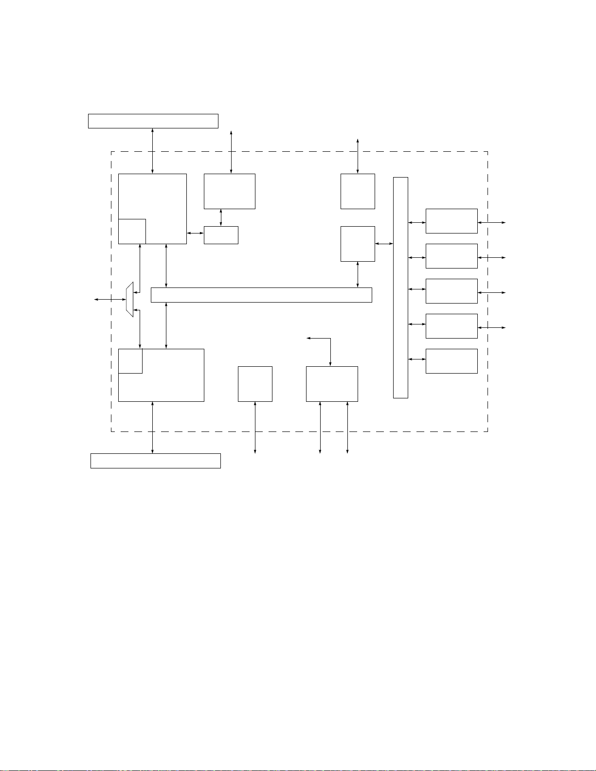
1.2 CPC700 Block Diagram
8
Parity
or
Arbiter
66MHz Processor Bus
119
Processor
Interface
Data
Parity
PCI
Arb
PCI
Interface
104
SDRAM
ROM
Peripherals
ECC
66MHz Processor Local Bus (PLB)
DCR Bus
JTAG
Misc.
(interrupts)
UIC
5
System
&
PLL
1/2X
OPB
Bridge
CPC700 ASIC
UART
UART
2
I
I2C
33MHz On Chip Peripheral Bus (OPB)
GPT
(Timers)
2
2
C
2
2
52
25 to 66MHz PCI Bus
1219
Figure 2. Functional Block Diagram
The block diagram illustrates the internal and external bus frequencies of the CPC700, given a 66MHz processor bus. Each of the blocks in the diagram represents a core from the IBM Blue Logic core library. The
architecture is based on two primary busses, the Processor Local Bus (PLB) and the On Chip Peripheral
Bus (OPB). The PLB operates at the same frequency as the local processor bus. The OPB operates at half
of the frequency of the PLB.
1-4 CPC700 User’s Manual—Preliminary
Page 21

Processor to PLB Interface
The CPC700 provides an interface to attach a 60x or 7xx processor to the internal PLB and to provide the
processor with a low latency access path to local memory. Through this interface, the processor may
access the PCI bus, local memory, external peripherals, and internal peripherals (UARTs, I2Cs, Timers,
and interrupt controller).
Processor interface features:
• Supports PowerPC 603e, 740, and 750 families.
• One level processor address pipelining.
• Support for processor “no-DR
• Processor bus arbiter arbitrates between local processor and internal snoop engine.
• L1 cache coherency support during PCI access to local memory.
• 32-byte write buffer to memory.
• 32-byte write buffer to PLB.
• lwarx/stwx. support (reservation cancelling snoops).
• Address only cycle support.
• External MCP_REQ input may be programmed to drive MCP to processor.
• Error tracking/status for processor transactions.
• Provides low latency access path to local memory.
Address Map Support
The CPC700 incorporates a simple fixed processor address map that serves the PowerPC family of processors. The address map has provisions for ROM, RAM, and I/O. Mapping does not require flexibility
because the CPC700 has the ability to map primary and secondary resources independently. This mapping can be performed solely from the processor side or from a combination of the processor and the PCI
side. This mechanism lets the same fixed secondary resources become flexible to the primary side, while
providing local processor operating space stability.
TRY” mode.
Through the use of “Mapping Port Windows,” either the PowerPC or PCI can gain access to the other
side’s resources. There are three local windows available to the PowerPC to access PCI memory. These
windows can be programmed to powers of 2 boundaries, are variable in size, and may be used to access
any location in a 64-bit PCI address space yet are invisible to the PCI bus.
PCI to local processor memory access “Port Windows” are handled in the PCI standard method, through
the programming of the Base Address Registers (BARs) in PCI configuration space. These registers are
defined to allow the PowerPC processor to request allocation of resources on the PCI side. There are
some fundamental differences though, that differentiate the CPC700 from other embedded solutions. The
first of these differences is that the PowerPC can program the size of the allocation as well as the type: I/O
or Memory. The second difference is that the actual location allocated by the host is translated to the PowerPC space via secondary registers allowing the PowerPC to maintain its local allocation independent of
PCI mappings.
There are two BARs available in the CPC700 for this function.
CPC700 User’s Manual—Preliminary 1-5
Page 22
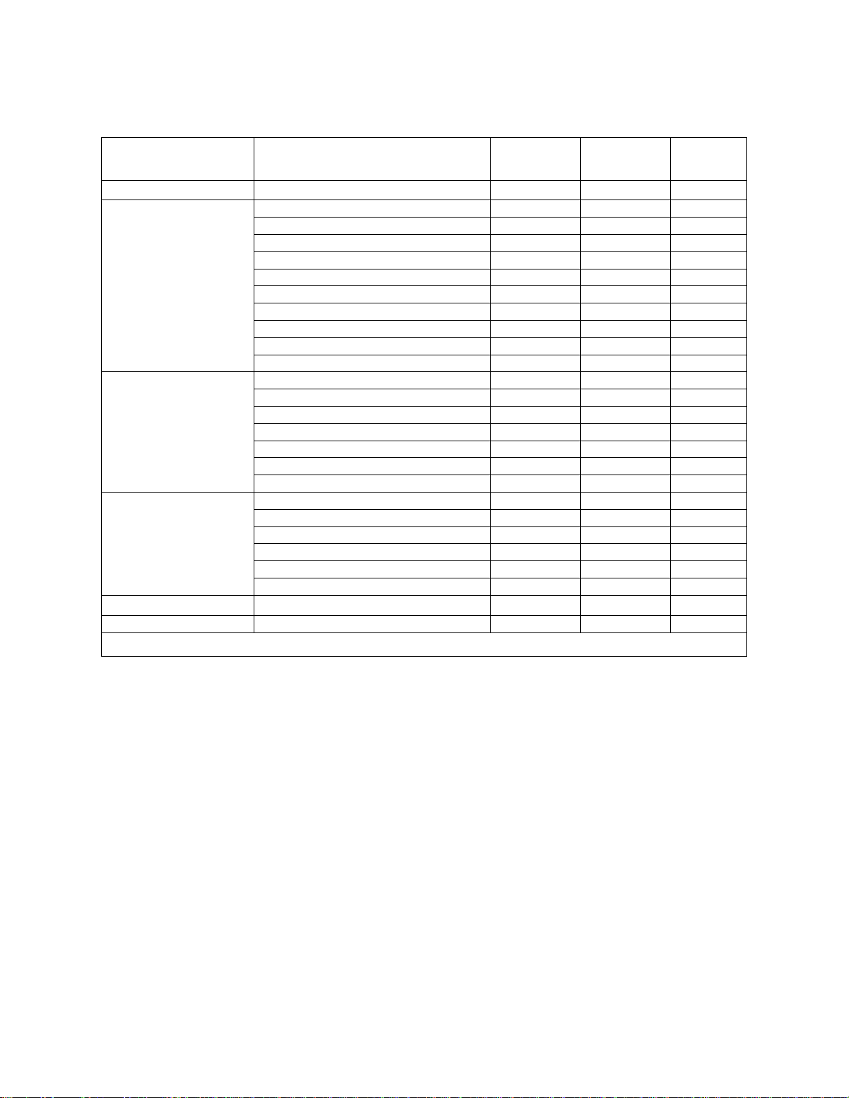
Table 1. Address Map
Start
Function Sub Function
Local Memory/Peripherals
PCI Core Space
Device Configuration
Register (DCR) Space
Internal Peripherals
Local Memory/Peripherals
Boot ROM FFE0 0000 FFFF FFFF 2MB
1. The Local Memory/Peripheral areas of the memory map may be configured for SDRAM, ROM, or Peripherals.
1
PCI Memory 8000 0000 F7FF FFFF
PCI I/O F800 0000 F800 FFFF
Reserved F801 0000 F87F FFFF
PCI I/O F880 0000 FBFF FFFF
Reserved FC00 0000 FEBF FFFF
PCI Configuration Registers FEC0 0000 FEC0 0004
PCI Interrupt Acknowledge FED0 0000 FEDF FFFF
Reserved FEE0 0000 FF3F FFFF
PCI local Configuration Registers FF40 0000 FF40 003C
Processor Interface Registers FF50 0000 FF50 0004
Memory Controller Registers FF50 0008 FF50 000C
OPB Macro Registers FF50 0810 FF50 0818
PLB Macro Registers FF50 0850 FF50 085C
Interrupt Controller FF50 0880 FF50 08A0
Clock and Power Management FF50 0900 FF50 0914
UART0 FF60 0300 FF60 0307
UART1 FF60 0400 FF60 0407
IIC0 FF62 0000 FF62 0010
IIC1 FF63 0000 FS63 0010
Timers FF65 0000 FF65 00FC
1
Address
0000 0000 7FFF FFFF 2GB
8000 0000 FF4F FFFF 2GB - 11MB
FF50 0000 FF5F FFFF 1MB
FF60 0000 FF7F FFFF 2MB
FF80 0000 FFDF FFFF 6MB
End
Address Size
PLB to PCI Interface
The PLB to PCI interface core provides a mechanism for connecting PCI devices to the local PowerPC
processor and local memory. This interface is compliant with version 2.1 of the PCI Specification. Features
of this core include:
• 32-bit PCI address bus
• PCI bus clock frequency from 25 to 66MHz
• Supports processor access to all PCI address spaces:
- Single-beat PCI I/O reads and writes
- PCI memory single-beat and prefetch-burst reads and single-beat writes.
- Single-beat PCI configuration reads and writes (type 0 and type 1)
- PCI interrupt acknowledge
- PCI special cycle
• Buffering between PLB and PCI:
- PCI target 32-byte write post buffer
- PCI target 32-byte read prefetch buffer
- PCI master 32-byte write post buffer
1-6 CPC700 User’s Manual—Preliminary
Page 23

- PCI master 64 byte read prefetch buffer
• Error tracking/status
• Internal PCI bus arbiter for up to six external devices at PCI bus speeds up to 33MHz. Internal arbiter
use is optional and may be disabled for systems which employ an external arbiter.
• Support for synchronous and asynchronous clocking between Processor and PCI busses. Support for
synchronous clocking is limited to a 33MHz PCI bus operation.
Memory Controller
The CPC700 Memory Controller provides the local PowerPC processor with a low latency access path to
local memory and external peripherals. In addition, it supports hardware coherent accesses to the processor’s local memory from the PCI bus. Coherency is maintained on PCI accesses to local memory by
snooping the processor’s L1 cache and posted write buffers before allowing the PCI interface to complete
the requested access.
Industry standard 72-pin and 168-pin modules are supported, allowing for a variety of system memory configurations. The memory controller supports up to five banks (five Chip Select outputs). Bank 0 is dedicated to Boot ROM, while banks 1-4 may be programmed to support either SDRAM, ROM, SRAM, or
external peripherals. Up to 512 MBytes per bank, are supported up to a maximum of 2 GBytes. Memory
timings, starting and ending address ranges, and memory addressing modes are programmable. During
reset, Bank 0 defaults to ROM and is enabled while all other banks are disabled.
Synchronous DRAM:
• Up to 4 banks (Bank 0 defaults to ROM).
• 11x9 to 13x11 addressing for SDRAM (2 and 4 bank internal SDRAM chip architecture supported).
• 8 MByte to 512 MByte per bank.
• Programmable timings and address mapping.
• CAS before RAS refresh w/programmable refresh timer.
• Supports hardware coherency.
• Page mode accesses.
• Sync DRAM configuration via mode set command.
• Memory bus operates at same frequency as processor bus.
• 64-bit and 32-bit memory interface options (72-bit or 40-bit if implementing ECC).
• Support for auto-precharge.
• Support for SRAM self-refresh mode (bank 4 only).
ROM/Peripheral:
• ROM, EPROM, SRAM, and Peripherals supported.
• Burst and Non-Burst devices.
• 1-5 banks (shared with SDRAM).
• 8-, 16-, 32-, and 64-bit data bus widths supported.
CPC700 User’s Manual—Preliminary 1-7
Page 24

• Programmable timing per bank.
• Shared address/data/control with SDRAM interface.
• External latch control for shared address bus support.
• Programmable address mapping.
• Peripheral Device pacing with external “Ready”.
ECC
The CPC700 generates, checks, and corrects ECC bits on their way to and from the memory controller.
Write cycles to memory that are less than a word in width require the ECC controller to generate a read
cycle to fetch the appropriate word, modify that word, generate the ECC bits, and write the word back out
to memory.
The ECC controller implements a 64-bit, single-error-correct, double-error-detect, over data and address.
ECC data is 8 bits wide.
• Corrects single-bit data errors.
• Detects double-bit data errors.
• Detects single-bit address errors.
• Detects concurrent single-bit address and single-bit data errors.
• Detects any errors within an aligned nibble.
• Eight check bits support 32- or 64-bit data bus widths.
• Support for mixing ECC and non-ECC DIMMs in the same system.
• ECC checking may be disabled.
UART
The CPC700 contains two UARTs that provide two wire, full duplex serial interfaces to support communications with serial peripheral devices. Each UART is compatible with the NS 16550 and includes a 16-byte
send and a 16-byte receive FIFO. Features of the UART include:
• Compatible with the NS 16550.
• 16-byte send FIFO, 16-byte receive FIFO.
• Full duplex operation.
• Programmable baud rate generator.
• Supports 5- to 8-bit word size, 1/2 stop bits, even/odd/no parity.
• Two wire transmit/receive external interface.
The UARTs perform serial-to-parallel conversion on data characters received from a peripheral device and
parallel-to-serial conversion on data characters received from the processor. The processor can read the
complete status of the UARTs at any time during the functional operation. Status information reported
includes the type and condition of the transfer operations being performed by the UARTs, as well as any
error conditions, such as parity, overrun, framing and break interrupt.
1-8 CPC700 User’s Manual—Preliminary
Page 25

The CPC700 UARTs are functionally identical to NS16450 in character mode (on power up they will be in
this mode). The UARTs can be put into FIFO mode to relieve the processor of excessive software overhead. Here internal FIFOs are activated, allowing 16 bytes (plus three bits per byte of error data in the
RCVR FIFO) to be stored in both receive and transmit modes. The timing reference clock is the CPC700
SYS_CLOCK input divided by 4. This will generally be 8.333MHz in a typical application (PowerPC local
processor operating with a 66MHz bus frequency).
The UARTs include a programmable baud rate generator capable of dividing the timing reference clock by
a divisor of 1 to (2
16
-1), and they produce a 16x clock for driving the internal transmitter logic. This 16x
clock can also be used to drive the receiver logic.
The UARTs have a processor interrupt system. Interrupts can be programmed to the user’s requirements,
minimizing the computing required to handle the communications link.
IIC Bus Interface
The CPC700 provides two fully independent IIC bus interfaces. The IIC bus is a two wire, bidirectional,
open-drain, low speed serial interface. Both the serial clock (SCL) and the serial data (SDA) lines are bidirectional to support multiple bus masters and to mix “fast“ and “slow” devices on the same bus. The
CPC700 IIC interfaces support the following standard and/or enhanced features of the Philips
ductors I
2
C Specification , dated 1995:
• 100 or 400 kHz operation.
• 8-bit data.
• 10- or 7-bit address.
• Slave transmitter and receiver.
• Master transmitter and receiver.
• Multiple bus masters.
®
Semicon-
• Two independent 4x1 byte data buffers.
• 12 memory mapped and fully programmable configuration registers.
• One programmable interrupt request signal.
• Provides full management of all IIC bus protocol
.
General Purpose Timers (GPT)
The General Purpose Timer (GPT) provides a separate time base counter and system timers for the
CPC700. Five capture timers and five compare timers are implemented in the GPT macro. Features of the
GPT core include:
• 32-bit time base.
- Updated once every CPC700 SYS_CLOCK.
• Five capture event timers.
• Five compare timers.
• 10 interrupt outputs, one for each capture and compare timer.
CPC700 User’s Manual—Preliminary 1-9
Page 26

Universal Interrupt Controller (UIC)
The Universal Interrupt Controller (UIC) provides the control, status, and communications necessary
between the various sources of interrupts and the local PowerPC processor. Features of the UIC include
the following:
• 29 interrupt sources.
- 12 external interrupts.
- 10 timer interrupts - five compare and five event capture.
- Two UART interrupts.
- Two IIC interrupts.
- PCI access to config register interrupt.
- PCI access to local memory interrupt.
- ECC correctable error interrupt.
• Interrupts are individually maskable.
• Interrupts can be individually programmed to generate a Machine Check Exception (MCP) or an External Interrupt (INT) to the processor.
• Interrupt types supported.
- Synchronous level sensitive.
- Synchronous edge-capture.
- Asynchronous- Choice of edge or level sensitive triggering is programmable.
• Polarity is programmable for all types.
• Prioritized interrupt handler vector generation.
• Status registers provide both of the following for interrupts.
- Current state of interrupts.
- Current state of all enabled interrupts (masked with Enable register).
Phase Locked Loop (PLL)
Table 2. PLL Usage
PLL Input Frequency Output Frequency Usage
PLL 0 33MHz
PLL 1 25MHz to 66MHz Same as input Async PCI Interface
The CPC700 clocking is controlled by two PLLs that minimize clock skew between the internal latches of
the CPC700 and the external devices in the system. PLL1 is only used when the PCI interface is used in
asynchronous mode. When in synchronous mode, PLL1 is placed in bypass mode via pin strappings, and
the PCI clock input pin must be pulled to ground.
33MHz UART, IIC, and Timers
66MHz All Other Cores
1-10 CPC700 User’s Manual—Preliminary
Page 27

JTAG
The IEEE 11.49.1 (JTAG) Boundary scan is included to facilitate tester requirements as well as for the
support of board level testing and debug.
The following JTAG commands are supported by the CPC700 JTAG TAP controller:
1. EXTEST
2. SAMPLE/PRELOAD
3. BYPASS
4. CLAMP
5. IDCODE
6. USERCODE
The CPC700 IDCODE value is 14940049. The CPC700 USERCODE value is 0.
Refer to IEEE 1149.1 specification for details on JTAG operation.
CPC700 User’s Manual—Preliminary 1-11
Page 28

1-12 CPC700 User’s Manual—Preliminary
Page 29

Chapter 2. Signal Descriptions
2.1 Processor Interface Signals
Active
Signal Name
Level I / O Description
DH[0:31] High I/O
DL[0:31] High I/O
DP[0:3] /
REQ[2:5]_N
DP[4:7] /
GNT[2:5]_N
- / Low I/O
- / Low I/O
Data Bus High: Processor Data bus - High 32 bits. The correspondence
of the processor data paths to byte lanes is as follows:
[DH0 - DH7] - Byte Lane 0
[DH8 - DH15] - Byte Lane 1
[DH16 - DH23] - Byte Lane 2
[DH24 - DH31] - Byte Lane 3
Data Bus Low: Processor Data bus - Low 32 bits. The correspondence
of the processor data paths to byte lanes is as follows:
[DL0 - DL7] - Byte Lane 4
[DL8 - DL15] - Byte Lane 5
[DL16 - DL23] - Byte Lane 6
[DL24 - DL31] - Byte Lane 7
Data Parity[0-3] / Request[2-5]: When the internal PCI arbiter is
disabled these signals carry the Processor Data Parity bits [0-3]. Odd
Parity is driven / received on the processor bus. The correspondence of
the Data parity pin to processor data paths is as follows:
DP0 - [DH0 - DH7]
DP2 - [DH8 - DH15]
DP3 - [DH16 - DH23]
DP4 - [DH24 - DH31]
If the internal PCI arbiter is enabled these signals carry the PCI Request
inputs [2-5] providing for a total of 6 PCI Request inputs.
Data Parity[4-7] / Grant[2-5]: When the internal PCI arbiter is disabled
these signals carry the Processor Data Parity bits [4-7]. The
correspondence of the Data parity pin to processor data paths is as
follows:
DP4 - [DL0 - DL7]
DP5 - [DL8 - DL15]
DP6 - [DL16 - DL23]
DP7 - [DL24 - DL31]
If the internal PCI arbiter is enabled these signals carry the PCI Grant
outputs [2-5] providing for a total of 6 PCI Grant outputs.
AP[0:3] - I/O
A[0:31] High I/O
Address Parity: Odd parity for each of the four bytes of the address
bus. The correspondence of the Address parity pins to processor
address bytes is as follows:
AP0 - [A0 - A7]
AP1 - [A8 - A15]
AP2 - [A16 - A23]
AP3 - [A24 - A31]
Address Bus:
Input: Represents the physical address of the data to be transferred.
Output: Represents the physical address of a snoop operation.
CPC700 User’s Manual—Preliminary 2-1
Page 30

Signal Name
Active
Level I / O Description
TT[0:4] High I/O
TSIZ[0:2] High I/O
ARTRY_N Low I/O
TBST_N Low I/O
GBL_N Low I/O
TS_N Low I/O
BR_N Low I
BG_N Low O
TA_N Low O
AACK_N Low O
T ransfer Type: Indicates the type of the transfer currently in progress.
Transfer Size: Indicates the data transfer size for the current operation.
Address Retry: This signal is asserted by either the processor or the
CPC700 to indicate that the current address tenure needs to be rerun at
a later time.
T ransfer Bur st: Indicates a burst transfer of f our 64-bit double-words on
the processor bus.
Global: This signal is asserted during snoop operations to indicate to
the processor that it must snoop the transaction.
Transfer Start: Asserted low for one clock cycle to signal a valid
address on the A[0:31] lines. This signal is an input when the local
processor initiates a cycle on the bus and acts as an output when the
CPC700 initiates a snoop cycle on behalf of a PCI master access to
local memory.
Bus Request: Processor bus request from the local processor.
Bus Grant: Grant output indicating that the local processor may assume
mastership of the processor bus.
Transfer Acknowledge: Indicates that a single-beat data transfer has
completed or that a data beat in a burst transfer completed successfully.
Address Acknowledge: Indicates that the address phase of a
transaction has completed.
DBG_N Low O Data Bus Grant: Indicates that the local processor may assume
mastership of the processor data bus.
MCP_N Low O Machine Check Pin: Indicates that an error condition has occurred and
that a machine check exception should be taken.
MCP_REQ High I Machine Check Interrupt Request: Input which may be used by an
external device to signal a machine check to the processor through the
MCP_N signal.
2-2 Signal Descriptions
Page 31

2.2 PCI Bus Interface Signals
Active
Signal Name
AD[31:0] High I/O Address/Data Bus: Address and data are multiplexed onto the same
C/BE_N[3:0] Low I/O Bus command and Byte Enables: Command and Byte Enables are
PAR High I/O Parity: Even parity across AD[0:31] and C/BE_N[0:3]. Parity is stable
FRAME_N Low I/O Frame: Driven by the current master to identify the beginning and
IRDY_N Low I/O Initiator Ready: Indicates the initiating agent’s ability to complete the
TRDY_N Low I/O Target Ready: Indicates the Target agent’s ability to complete the
STOP_N Low I/O STOP: Indicates the current target is requesting the master to stop the
Level I / O Description
PCI pins. A bus transaction consists of an address phase followed by
one or more data phases.
multiplexed on the same pins. During the address phase of a
transaction, C/BE[0:3] define the bus command and during the data
phase they carry the bus byte enables.
and valid one clock after the address phase.
duration of an access.
current data phase of the transaction.
current data phase of the transaction.
current transaction.
DEVSEL_N Low I/O Device Select: When actively driven, indicates the driving device has
decoded its address as the target of the current access.
IDSEL High I Initialization Device Select: Used as a chip select during configuration
read and write transactions
SERR_N Low I/O System Error: May be used for reporting address parity errors, data
parity errors on special cycle commands, or other error where the result
will be catastrophic.
PERR_N Low I/O Parity Error: Data parity error.
PCI_CLK -- I Asynchronous PCI Clock: Clock input required for use when the PCI
bus is run asynchronously from the processor bus. When operating in
synchronous mode, this pin is not used and should be tied low.
RST_N Low O PCI RESET: This output ma y be used as the reset to PCI b us slots when
the CPC700 is used as the primary host bridge. This signal will be
asserted during three scenarios:
1. Power on Reset: Following the deasertion of SYS_RESET_N,
RST_N will remain active for a period of 500us while the internal
PLLs lock after which, this signal will be deaserted.
2. Software Control: Setting PCI Bridge Options 2 register bit 12 high
will cause RST_N to assert. Resetting bit 12 to zero will deassert
RST_N.
3. PLL Tuning Bits Change: If the PLL tuning bits are changed under
software control, the CPC700 will enter the reset state similar to a
power on reset sequence. RST_N will remain asserted for 500us.
CPC700 User’s Manual—Preliminary 2-3
Page 32

Signal Name
Active
Level I / O Description
REQ0_N/
GNT_N
REQ1_N Low I Request[1]: When the internal PCI arbiter is enabled, this signal
GNT0_N/
REQ_N
Low I Request[0] / Grant: When the internal PCI arbiter is enabled, this signal
functions as the Request[0] input from another PCI master device.
When the internal PCI arbiter is disabled and an external arbiter is
employed, this signal is the Grant input f or the CPC700 from the e xternal
arbiter.
functions as the Request[1] input from another PCI master device. If the
PCI internal arbiter is not used, this signal is not used and should be
pulled high.
The internal PCI arbiter provides arbitration for 6 PCI master devices.
Request inputs [2-5] are multiplexed with the processor Data Parity
signals. If processor data parity is enabled, the internal PCI arbiter will
be disabled.
Low O Grant[0] / Request: When the internal PCI arbiter is enabled, this signal
functions as the Grant[0] output to another PCI master device.
When the internal PCI arbiter is disabled and an external arbiter is
employed, this signal is the Request output for the CPC700 to request
the use of the PCI bus.
The internal PCI arbiter provides arbitration for 6 PCI master devices.
Grant outputs [2-5] are multiplexed with the processor Data Parity
signals. If processor data parity is enabled then the internal PCI arbiter
will be disabled.
GNT1_N Low O Grant[1]: When the internal PCI arbiter is enabled, this signal functions
as the Grant[1] output from the CPC700 to another PCI master device. If
the PCI internal arbiter is not used, this signal is not used.
PCI_66_STRAP High I 66MHz Operation Strap: This signal is used to indicate to the CPC700
that the PCI bus is operating at higher than 33MHz.
2-4 Signal Descriptions
Page 33

2.3 Memory Interface Signals
Active
Signal Name
M_DATA[0:63] High I/OMemory Data: 64-bit memory data bus. If configured for a 32-bit memory
ECC[0] High I/OError Correction Code Data[0]: Bit [0] of the 8-bit Error correction code
DQM[0] High O SDRAM Data Mask[0]: Data byte mask bus bit 0. This bit is connected to all
ECC/DQM[1:7] High I/OECC[1:7] / DQM[1:7]: Multiplexed ECC and DQM bit [1:7]. The use of either
MA[12:0] High O Memory Address[12:0]: Memory address bus. Memory address bit 10 also
Level I/O Description
interface, M_DATA[0:31] are used.
data bus. Bits [1:7] are multiplexed with the DQM bus bits [1:7]. If ECC is
enabled a single DQM (bit 0) is connected to all DQM inputs on all DIMMs.
DQM inputs of all DIMMs if ECC is used in the system. If ECC is not used,
then ECC/DQM[1:7] lines make up the remainder of the 8-bit DQM bus.
DQM[0] corresponds to Memory Data Lane 0. During reads, the CPC700
asserts DQM high to cause the SDRAM to tristate the SDRAM output. If
DQM is low, the SDRAM drives the data onto the output.
During writes, DQM high commands the SDRAM to mask the data. The input
data is ignored and the previous contents of the SDRAM are retained. When
DQM is low during a write, the SDRAM data is updated as usual.
ECC or the additional DQM lines are governed by a pin strapping option.
DQM7 corresponds to Memory Data Lane 7
functions as the auto-precharge bit. Signal range is in little endian notation.
BANK_SEL_N
[0:4]
WE_N Low O Write Enable: SDRAM Write Enable.
CKE High O Clock Enable: SDRAM Clock Enable.
RAS_N Low O Row Address Strobe: SDRAM Row Address Strobe.
CAS_N Low O Column Address Strobe: SDRAM Column Address Strobe.
BA[1:0] High O Bank Address[1:0]: SDRAM Bank Address. The Bank Address accesses
ROM_OE_N Low O ROM Output Enable: Output enable for ROM / Peripheral devices.
ROM_WE_N Low O ROM Write Enable: Write enable for ROM / Peripheral devices.
ROM_RD_N Low O ROM Read: Read signal for ROM / Peripheral devices.
ROM_WR_N Low O ROM Write: Write signal for ROM / Peripheral devices.
ROM_RNW High O ROM Read-Not-Write: The ROM_RNW signal may be used as a direction
Low O Memory Bank Select[0:4]: Five Banks are supported with bank 0 required
to contain the boot ROM device. The remaining 4 banks ma y be programmed
for SDRAM, ROM/Flash, SRAM, or peripheral devices.
one of up to 4 internal banks within an SDRAM chip. Signal range is in little
endian notation.
indicator for external data bus transceivers in the event that the system
designer chooses to isolate the ROM / Peripheral bus from the SDRAM data
bus.
CPC700 User’s Manual—Preliminary 2-5
Page 34

ROM_ALE High O ROM Address Latch Enable: When accessing a bank which is programmed
for ROM, SRAM, or peripheral devices, the 24-bit memory address bus is
provided in two cycles. The 12-bit address on pins MA[12,11,9:0] bus must
be latched on the first cycle in order capture and hold the higher order
address bits of the ROM / peripheral address. The ROM_ALE signal may be
used as a latch enable for an external address bus latch to capture those
signals.
ROM_READY High I ROM Ready: External ready indicator from a device paced peripheral.
2.4 Internal Peripherals Interface Signal
Active
Signal Name
UART0_TX High O UART0 Transmit
UART1_RX High I UART1 Receive
UART0_TX High O UART0 Transmit
UART1_RX High I UART1 Receive
IIC0_SCL High I/O IIC0 Clock
IIC0_SDA High I/O IIC0 Data
Level I / O Description
IIC1_SCL High I/O IIC1 Clock
IIC1_SDA High I/O IIC1 Data
2-6 Signal Descriptions
Page 35

2.5 System Interface Signals
Active
Signal Name
SYS_CLOCK — I System Clock Input: The system clock input must be one half the
SYS_RESET_N Low I System Reset Input: Resets the CPC700 to its initial default state. The
RESET_OUT_N Low O Reset Output: RESET_OUT_N follows the internal reset and will be
IRQ[0:11] High I Interrupt Input [0:11]: Twelve external interrupts may be attached and
IRQ_OUT_N Low O Interrupt Output: Interrupt output to the local processor.
Level I / O Description
frequency and in phase with the local processor and SDRAM clocks.
internal reset will remain active for 500us after the SYS_RESET_N
signal is deasserted.
driven for 500us after the SYS_RESET_N signal is deasserted.
RESET_OUT_N will also be driven in the event that the PLL tuning bit
register is written so that the internal PLLs may re-lock with the new
configuration. After RESET_OUT_N is deasserted, the CPC700 will be
in its initial default state. The RESET_OUT_N signal should drive into
the processor’s hard reset logic.
allowed to interrupt the processor. These interrupt inputs are
asynchronous and may be programmed to cause an interrupt on either
the rising or falling edge.
SYSPLL_VDDA High I System Clock PLL Analog Voltage Pin: The analog voltage pin for the
System PLL must be connected to a quiet voltage. Typically this voltage
should be isolated from the system digital voltage plane.
PCIPLL_VDDA High I Async PCI Clock PLL Analog Voltage Pin: The analog voltage pin for
the asynchronous PCI PLL must be connected to a quiet voltage.
Typically this voltage should be isolated from the system digital voltage
plane.
2.6 Test Interface Signals
Active
Signal Name
TDI High I JTAG Test Data Input
TMS High I JTAG Test Mode Select
TDO High O JTAG Test Data Output
TCK High I JTAG Test Clock
TRST_N Low I JTAG Test Reset: Reset for JTAG controller. Must be activated during
Level I / O Description
system reset or tied low during operation.
1
1
1
2
TEST_ENABLE High I LSSD Test Mode Enable: The test enable pin is only used during
manufacturing test and must be low during operation. There is an
internal 13K Ω pull-down on this signal. Either leave this pin floating, or
connect it to a 10K Ω pull-down.
3
CPC700 User’s Manual—Preliminary 2-7
Page 36

RI_N Low I Receiver Inhibit: The receiver inhibit pin is only used during
manufacturing test. This signal has no internal pull-up. Pull up this signal
to 3.3V with a 10K Ω resistor.
3
DI1_N Low I Driver Inhibit 1: The driver inhibit 1 pin is only used during manuf acturing
test and must be high during functional operation. There is an internal
20K Ω pull-up to 3.3V on this signal. Either leave this pin floating, or pull
it up to 3.3V with a 22K Ω resistor.
3
DI2_N Low I Driver Inhibit 2:The driver inhibit 2 pin is only used during manufacturing
test and must be high during functional operation. There is an internal
20K Ω pull-up to 3.3V on this signal. Either leave this pin floating, or pull
it up to 3.3V with a 22K Ω resistor.
3
Notes:
1. We recomment attaching a 10K Ω pullup to 3.3V to this signal.
2. One way to assert TRST_N whenever RESET_N is active, is to set TRST_N=RESET_N And TRST (from
JTAG probe).
3. Because the boundary scan function of the JTAG port does not work in dd 1.1 of the CPC700, we strongly
recommend that this signal be brought out from the solder ball to at least a via, so that a board tester can
drive the signal.
2-8 Signal Descriptions
Page 37

Chapter 3. Processor Interface
The processor interface is the portion of the CPC700 that attaches a PowerPC 60x or 7xx processor to the
internal PLB and the local memory controller. Through this interface, the processor may access the PCI
bus, local memory, and the CPC700’s internal peripherals (UARTs, I2C ports, timers, and interrupt controller).
3.1 Features
Processor:
• PowerPC 603, 740, and 750 families
• 1 level processor address pipelining
• Support for processor “no-DRTRY” mode
• Processor Bus Arbiter (for Processor Interface core & snooping) w/ processor parking
• L1 cache coherency support
• 32 Byte Write Buffer to memory
• 32 Byte Write Buffer to PLB
• lwarx/stwcx. support (reservation cancelling snoops)
• Address Only cycle support
• Machine Check Interrupt request input (MCP_REQ) for processor error reporting
• Error tracking/status for processor transactions
PLB Interface
• PLB Master interface provides access to the PCI bus from the processor
• PLB Master interface provides access to internal peripherals from the processor
• PLB Slave interface provides access to the system memory from the PCI bus
Memory Interface
• Low latency access path to local memory
• Maintains coherency with the processor’s L1 cache during PCI accesses to local memory.
3.2 Processor Interface Block Diagram
A detailed view of the function contained within the processor to PLB interface is shown in the block diagram in Figure 3.
CPC700 User’s Manual—Preliminary 3-1
Page 38

NOTE: W.B.=Write Buffer; R.B.=Read Buffer
Processor Bus
Processor Interface
DCR Bus
DCR
Master
DCR Slave
CONFIG Regs
PLB
W.B.
PLB Master
Interface
PLB Master
Bus
R.B.
Mem
W.B.
Central
Arbiter/
Snooper
R.B.W.B.
PLB Slave
Interface
PLB Slave
Bus
MC
I/F
To
Memory Controller
Figure 3. Processor Interface Detailed Block Diagram
3.3 Processor Interface Registers
Processor interface registers are accessed through an indirect method employing a configuration address
register, PIFCFGADR, and a configuration data register, PIFCFGDATA. To access one of the processor
interface registers, write the appropriate index to register PIFCFGADR, then read the data from or write the
data to register PIFCFGDATA. All configuration accesses from the processor must be 4 Byte aligned, otherwise an error will be generated and the cycle not performed.
Table 3. Processor Interface Register Addressing
Register Address R/W Description
PIFCFGADR FF50_0000 R/W Processor Interface Configuration Address Register
PIFCFGDATA FF50_0004 R/W Processor Interface Configuration Data Register
Table 4 lists the offsets for the various configuration registers located within the processor interface.
Table 4. Offsets for Processor Interface Registers
Register Offset R/W Description
PRIFOPT1 00 R/W Processor Interface Options 1
ERRDET1 04 R/W Error Detection 1
ERREN1 08 R/W Error Detection Enable 1
CPUERAD 0C R Processor Error Address
CPUERAT 10 R Processor Error Attributes
Reserved 14
PLBMIFOPT 18 R/W Processor-PLB Master Interface Options
PLBMTLSA1 20 R/W Processor-PLB Master Byte Swap Region 1 Starting Address
3-2 Processor Interface
Page 39

Table 4. Offsets for Processor Interface Registers (Continued)
Register Offset R/W Description
PLBMTLEA1 24 R/W Processor-PLB Master Byte Swap Region 1 Ending Address
PLBMTLSA2 28 R/W Processor-PLB Master Byte Swap Region 2 Starting Address
PLBMTLEA2 2C R/W Processor-PLB Master Byte Swap Region 2 Ending Address
PLBMTLSA3 30 R/W Processor-PLB Master Byte Swap Region 3 Starting Address
PLBMTLEA3 34 R/W Processor-PLB Master Byte Swap Region 3 Ending Address
PLBSNSSA0 38 R/W PLB Slave No Snoop Region Starting Address
PLBSNSEA0 3C R/W PLB Slave No Snoop Region Ending Address
BESR 40 R/W PLB Bus Error Syndrome Register
BESRSET 44 W PLB Bus Error Syndrome Register Set (for test/verification
use)
Reserved 48
BEAR 4C R/W PLB Bus Master Error Address Register
Reserved 50
Reserved 54
PLBSWRINT 80 R/W Write Interrupt Region Base Address
Detailed information regarding the processor interface registers can be found in Section 3.16, “Processor
Interface Register Description”.
3.4 Processor Interface to Memory, PCI, and Peripherals
The CPC700 supports 1 full level of addressing pipelining on the processor bus and decodes the target of
processor accesses based on the address range of the transfer. All of the processor accesses are decoded
as one of the following:
• System memory read (SDRAM/ROM)
• System memory write (SDRAM/ROM)
• DCR configuration read
• DCR configuration write
• PLB read (PCI or internal peripherals)
• PLB write (PCI or internal peripherals)
The range of addresses that define the above accesses are defined by the address map detailed in the following tables.
Table 5. CPC700 Address Map - Processor View
PLB
Processor Address Range Description
0 to
2G-1
h00000000
h7FFFFFFF
System Memory
Typically reserved for local memory
Address
2G to
4G-11M-1
CPC700 User’s Manual—Preliminary 3-3
h80000000
hFF4FFFFF
PCI Interface* h80000000
hFF4FFFFF
Page 40

Table 5. CPC700 Address Map - Processor View (Continued)
Processor Address Range Description
PLB
Address
4G-11M to
4G-10M-1
4G-10M to
4G-8M-1
4G-8M to
4G-2M-1
4G-2M to
4G-1
* Accesses to this region are affected by the following configuration registers:
• PLBMIFOPT
• PLBMTLSA1
• PLBMTLEA1
• PLBMTLSA2
• PLBMTLEA2
• PLBMTLSA3
• PLBMTLEA3
hFF500000
hFF5FFFFF
hFF600000
hFF7FFFFF
hFF800000
hFFDFFFFF
hFFE00000
hFFFFFFFF
DCR - Configuration Address/Data
Internal Peripherals hFF600000
System Memory
Typically reserved for ROM/External Peripherals
System Boot ROM
hFF7FFFFF
Table 6. CPC700 Address Map - PCI View
PLB Address Range Description
0 to
2G-1
2G to
4G-2M-1
4G-2M to
4G-1
h00000000
h7FFFFFFF
h80000000
hFFDFFFFF
hFFE00000
hFFFFFFFF
System Memory
PCI accesses to this range will target system
memory and be snooped. Snooping can be disabled for a particular region using the PRIFOPT1,
PLBSNSSA0, PLBSNSEA0 registers.
Reserved
The processor interface does not respond to accesses in this range.
System Memory (Boot ROM)
PCI accesses to this range will target system
memory and be snooped. Snooping can be disabled for a particular region using the PRIFOPT1,
PLBSNSSA0, PLBSNSEA0 registers.
Processor
Address
h00000000
h7FFFFFFF
hFFE00000
hFFFFFFFF
3-4 Processor Interface
Page 41

3.5 Supported Processor Transfer Types
Based on signals TT[0:3] (see Table 7), the CPC700 responds to processor initiated transfers by generating a read transaction, a write transaction, or an address-only response. The CPC700 ignores TT[4] when
evaluating processor initiated transfers.
The CPC700 supports all processor to memory/PLB bursts and all single-beat transfer sizes and alignments
that do not cross a 4-byte boundary. The following table lists all supported processor transfer types and the
corresponding response from the CPC700.
NOTE: In Table 7, SBR is single-beat read and SBW is single-beat write.
Table 7. Supported Processor Transfer Type Encodings/Response
Processor
TT[0:3]
0000 Clean block or lwarx Address only Assert AACK_N, No other response, No PLB
0001 Write with flush SBW or burst Memory write PLB write
0010 Flush block or stwcx Address only Assert AACK_N, No other response, No PLB
0011 Write with kill SBW or burst Memory write PLB write
0100 sync or tlbsync Address only Assert AACK_N, No other response
0101 Read or read with no
0110 Kill block or icbi Address only Assert AACK_N, No other response, No PLB
0111 Read with intent to
1000 eieio Address only Assert AACK_N, No other response
Operation
intent to cache
modify
Proc Bus
Transaction
SBR or burst Memory read PLB read
Burst Memory read PLB read
CPC700 Response for
Proc to Memory
transaction
transaction
transaction
CPC700 Response for
Proc to PLB
1001 Write with flush
atomic, stwcx
1010 ecowx SBW Reserved
1011 Reserved Reserved
CPC700 User’s Manual—Preliminary 3-5
SBW Memory write PLB write
Assert AACK_N and TA_N. MCP_N asserted if
MCP_N assertion is enabled.
Assert AACK_N and TA_N. MCP_N asserted if
MCP_N assertion is enabled.
Page 42

Table 7. Supported Processor Transfer Type Encodings/Response (Continued)
Processor
TT[0:3]
1100 TLB invalidate Address only Assert AACK_N, No other response, No PLB
1101 Read atomic, lwarx SBR or burst Memory read PLB read
1110 External control in,
1111 Read with intent to
Please refer to the processor’s user’s manual for additional information on transfer type encodings.
Operation
eciwx
modify atomic, stwcx
Proc Bus
Transaction
SBR Reserved
Burst Memory read PLB read
CPC700 Response for
Proc to Memory
transaction
Assert AACK_N and TA_N. All 1’s returned on
60x Data Bus. MCP_N asserted if MCP_N assertion is enabled.
CPC700 Response for
Proc to PLB
3.6 Processor to Memory
The processor interface contains a single 32 byte write buffer and a single 8 byte read buffer for processor
accesses to system memory. Once the processor has gained access to memory for a given transfer, the
memory is unavailable for PCI to memory transfers or subsequent processor to memory transfers until the
address tenure of the current access completes.
Reads: Processor to memory read (single beat and burst) data is buffered in the 8 byte read buffer which
captures the data directly from the memory bus and drives the data onto the processor bus in the next
clock cycle. All processor to memory read cycles execute as connected data tenures between the processor bus and the memory bus.
Writes: All processor write (burst or single beat) cycles are posted. All processor memory read cycles (single beat and burst) which hit in the posted write buffer, flush the write buffer contents to memory. All single
beat write cycles flush the posted write buffer (if allocated) before completing. Prior to allowing a PCI
access to system memory, the 32 byte posted write buffer is snooped in addition to the processor’s L1
cache.
Write Buffer: Once data is posted in the processor to memory write buffer it is flushed to memory at the
earliest available opportunity. In general, the posted write buffer has the lowest priority for access to system memory; however, the low priority write buffer flush may transition to a high priority write buffer flush
under the following circumstances:
1. Processor to memory read hit in write buffer
2. Any processor to memory write
3. PCI to memory read hit/write hit in write buffer or processor L1
4. Processor read/write to PLB or DCR configuration space
5. If no memory controller requests from the processor and PCI, and memory controller interface is
idle.
6. Snoop push detected.
Note: The processor to memory write buffer is not flushed to system memory until a high priority write
buffer flush request is generated.
3-6 Processor Interface
Page 43

3.6.1 CPC700 Response for Processor to System Memory Accesses
The following table corresponds to the state of the processor address bus for a given cycle (which may or
may not be pipelined) and the corresponding response from CPC700. NOTE: For any of the transactions
listed, the internal memory controller interface may be idle or busy (servicing a processor to memory write
buffer flush or finishing the data tenure of a previous PCI or processor access to system memory). If the
internal memory controller interface (MCIF) is busy, the address for the processor to memory access is
placed on the MCIF as soon as possible. The data tenure for the requested access will execute on the
MCIF following the completion of the in progress data tenure.
Once the processor request is accepted, as indicated by the assertion of AACK_N to the processor, data
will be transferred at the earliest available opportunity.
Note: In Table 8., the state of the processor to PLB write buffer is a “don’t care.”
Table 8. CPC700 Response for processor to System Memory Transactions
Proc-Mem
Proc
Mem Rd Deallocated AACK_N CPU and return data from system memory
W.B. Response
Mem Rd Allocated,
Miss
Mem Rd Allocated,
Hit
Mem Wr Deallocated
Mem Wr Allocated,
Miss
Mem Wr Allocated,
Hit
Bypass processor-Mem W.B., AACK_N CPU and return data from system memory
ARTRY_N CPU, High Priority write for processor-Mem W.B. flush
Post write in
ARTRY_N CPU, High Priority write for processor-Mem W.B. flush
ARTRY_N CPU, High Priority write for processor-Mem W.B. flush
processor-Mem W.B.
Table 9. lists the corresponding memory controller interface requests generated in response to processor
requests to/from system memory.
Table 9. Processor to Memory Cycle Translation
Processor to MEM Transfer (Rd or Wr) Memory Controller I/F Request
Single Beat Doubleword with byte enables
Burst(32 byte) Quad Doubleword (wrap within cache line)
CPC700 User’s Manual—Preliminary 3-7
Page 44

3.7 Processor to PLB Master (PCI or Internal Peripherals)
The CPC700 supports single beat (8 bytes or less) and burst (32 byte cache line) read and write accesses
to the PLB. Processor requests that target PLB space are forwarded to the PLB Master interface which initiates a request on the PLB bus for the associated cycle. The PLB master interface contains a single 32
byte write buffer, a single 8 byte write interface buffer, and a single 32 byte read buffer for processor
accesses to the PLB.
Reads:
Processor to PLB read (single beat and burst) data is buffered in a 32 byte read buffer which captures the
data directly from the PLB bus. All processor to PLB read cycles execute as connected data tenures
between the processor bus and the PLB bus. The processor address tenure remains open until the targeted PLB Slave commits to returning the requested data via the assertion of PLB_AddrAck.
Writes:
All processor to PLB write (burst and single beat) cycles are posted and executed on the PLB at the earli-
est available opportunity. The CPC700’s processor interface contains an 8 byte write interface buffer to
expedite de-allocation of the primary 32 byte write buffer which allows the processor to post a maximum of
two single beat write cycles for transfer to the PLB . All processor to PLB read cycles (single beat and burst)
and write cycles flush the primary 32 byte write buffer and 8 byte write interface buffer (if allocated) contents to the PLB before completing. For more information, see Table 10.
Table 10. PLB Master Cycles
64-Bit Processor Interface PCI Interface
Single Beat (1-4 Bytes) 1 (Single Beat)
5-8 Bytes 2 Single Beats
32 Byte 1 Eight Word Line
3.7.1 CPC700 Response for Processor to PLB Accesses
The following table corresponds to the state of the processor address bus for a given cycle (which may or
may not be pipelined) and the corresponding response from CPC700.
Once the processor request is accepted, as indicated by the assertion of AACK_N to the processor, data
will be transferred at the earliest available opportunity.
Note: In Table 11., the status of the processor to memory write buffer is a “don’t care.”
.
Table 11. CPC700 Response to Processor Transactions to the PLB
Proc
I/F
Proc-PLB
Read
Buffer
Proc-PLB
Write
Buffer
PLB
Slave
(Snoop) Response
PLB Rd Deallocated Deallocated Idle Request PLB for read, AACK_N CPU when PLB AdrACK_
3-8 Processor Interface
and transfer data, or ARTRY_N CPU if PLB Rearbitrate
Page 45

Table 11. CPC700 Response to Processor Transactions to the PLB (Continued)
Proc-PLB
Proc
I/F
PLB Rd Deallocated Deallocated Snoop
PLB Rd Deallocated Allocated Idle Continue to attempt write on PLB, Hold 60x read and ini-
PLB Rd Deallocated Allocated Snoop
PLB Rd Allocated Deallocated Idle Request PLB for read, AACK_N CPU when PLB AdrACK_
PLB Rd Allocated Deallocated Snoop
PLB Rd Allocated Allocated Idle Continue to attempt write on PLB, initiate read on PLB
PLB Rd Allocated Allocated Snoop
PLB Wr D.C. Deallocated D.C. AACK_N CPU, post write data in 60x-PLB W.B., initiate
PLB Wr D.C. Allocated Idle Continue to attempt posted write on PLB, hold pending
Read
Buffer
Proc-PLB
Write
Buffer
PLB
Slave
(Snoop) Response
Pending
Pending
Pending
Pending
ABORT PLB read cycle, ARTRY_N CPU, grant to snooper
tiate on PLB once PLB write completes.
ARTRY_N CPU, grant to snooper, continue to attempt
write on PLB
and transfer data, or ARTRY_N CPU if PLB Rearbitrate
ABORT_ PLB read cycle, ARTRY_N CPU, grant to snoop-
er
when write completes
ARTRY_N CPU, grant to snooper, continue to attempt
write on PLB
write on PLB at earliest available opportunity.
60x-PLB write address tenure open until write buffer deallocates (post pending write data) or snoop pending
(ARTRY_N pending cpu write)
PLB Wr D.C. Allocated Snoop
Pending
D.C. - Don’t Care
ARTRY_N CPU, grant to snooper, continue to attempt
posted write on PLB
CPC700 User’s Manual—Preliminary 3-9
Page 46

Table 12. lists the corresponding PLB Master interface requests generated in response to processor requests which target the PLB.
Table 12. Processor to PLB Cycle Translation
Processor to PLB Transfer PLB Transfer
32-bit Slave Responds
Read 1-4 Bytes
Word Address 0
CPU_A(29:31)=000
Read 1-4 Bytes
Word Address 1
CPU_A(29:31)=100
Read 2-8 Bytes
Crossing Word Boundary
Read 32 Bytes
(8 Word Line)
Write 1-4 Bytes
Word Address 0
Write 1-4 Bytes
Word Address 1
Write 2-8 Bytes
Crossing Word Boundary
1-4 byte read w/byte enables,
Read data transferred to CPU_DATA[0:31]
1-4 byte read w/byte enables,
Read data transferred to CPU_DATA[32:63]
2-8 byte read w/byte enables,
Request W0 Read data, transfer to CPU_DATA[0:31]
Request W1 Read data, transfer to CPU_DATA[32:63]
8 word line read consisting of 8 PLB data phases,
Read data transferred to CPU_DATA[0:63]; indicate word being transferred. Only 1 word transferred per PLB data phase
Not applicable to PCI
1-4 byte write w/byte enables,
Write data transferred from CPU_DATA[0:31]
1-4 byte write w/byte enables and data replicated on Word Lane 0,
Write data transferred from CPU_DATA[32:63]
2-8 byte write w/byte enables,
Request W0 Write, transfer data from CPU_DATA[0:31]; queue PLB
write for W1; request PLB; request W1 Write, transfer data from
CPU_DATA[32:63]
Write 32 Bytes
(8 Word Line)
8 word line write consisting of 8 PLB data phases,
Write data transferred from CPU_DATA[0:31] for Word 0 and from
CPU_DATA[32:63] for Word 1.Only 1 word transferred per PLB data
phase
Not applicable to PCI
3.8 Processor - Address Only Cycles
The CPC700 supports all processor generated Address Only cycles. In response to a processor Address
Only cycle, CPC700 acknowledges the cycle and takes no other action. As a result, CPC700 does not propagate any Address Only cycles beyond the processor bus interface.
3-10 Processor Interface
Page 47

.
Table 13. CPC700 Response to Processor Address Only Cycles
Proc
Cycle
Addr Only D.C. D.C. D.C. AACK_N CPU immediately, no other ac-
D.C. - Don’t Care
Proc-Mem
WriteBuffer
Proc-PLB
WriteBuffer
PLB Slave
(Snoop) Response
tion
3.9 Processor Bus Arbiter
The CPC700’s processor interface logic contains the processor bus arbiter which controls access to the
local processor bus. It arbitrates between processor requests and the internal snoop engine (PCI to memory) requests.
Arbitration for the bus for processor requests or the internal snoop engine is based on a rotating priority
scheme to ensure fairness and guarantee that each requesting device is given an equal opportunity to
access the bus in the event of simultaneous requests from multiple devices as viewed by the arbiter. The
bus arbiter implements bus parking for the processor in that it continuously asserts bus grant to the processor during the periods when there are no requests from either the PCI or processor bus. In this case the
arbitration fav ors the processor in that it ma y begin a bus tr ansaction without e xplicitly requesting access to
the bus. The bus arbiter recognizes the instances when the processor initiates a bus transaction while
parked as an implicit bus request which was granted and maintains the rotating priority accordingly.
In general the priority is controlled by a rotating token which tracks the least recently granted device. Following Power-on Reset, the token defaults to the processor and attempts to park the processor address
bus. If the PCI/Snooper requests access to system memory, the arbiter removes the CPU bus grant, waits
to see if the processor begins an access and simultaneously rearbitrates to grant the bus to the PCI/
Snooper. The following table details the arbiter response for the request/grant scenarios.
Table 14. Processor Address Bus Arbitration
Least Recently
Request
CPU Only D.C. CPU May be parked.
PCI/Snooper
Only
CPU and PCI/
Snooper
CPU and PCI/
Snooper
None D.C. CPU Bus Parked on CPU
D.C. - Don’t Care
CPC700 User’s Manual—Preliminary 3-11
Granted Granted Comment
D.C. PCI/Snooper If processor bus parked, remove CPU grant,
grant to PCI/Snooper
PCI/Snooper PCI/Snooper
CPU CPU
Page 48

Requests from the processor are treated as implied requests for access to system memory. As such, arbitration of processor and PCI requests indicates that the associated device receiving the grant is guaranteed
the next access to system memory once any in-progress access completes. For PCI accesses to system
memory, the PCI/Snooper, once granted the processor address bus, retains ownership of the address bus
for the duration of the PCI to memory transfer. Specifically, this applies to PCI Burst accesses, during which
the processor address bus ownership is required to allow snooping of burst accesses which attempt to cross
a cache line boundary.
3.10 Broadcast Snoop Cycles
The CPC700 supports PCI accesses to system memory via the PLB Slave interface. Memory coherency is
maintained by the internal snoop engine. PCI requests which address system memory are accepted and
snooped in the processor's L1 cache before allowing the access. Snoop cycles to the processor are generated on behalf of the PCI interface by the internal snooper. The following table lists the corresponding snoop
transfer type for PCI accesses to system memory.
Table 15. Processor Snoop Transfer Types
PLB Bus Cycle Processor Bus Snoop Cycle Processor Snoop TType[0:4]
Memory Read Single-Beat Read 01010
Memory Write Single-Beat Write
with Flush
To perform a snoop cycle to the processor, the snoop engine must arbitrate for the processor bus. Once
access has been granted and the address bus is available, the snoop engine will proceed with the snoop
cycle. If a processor access to system memory is in progress, the transfer is allowed to complete. If a processor access to the PLB is in progress and a PLB Slave device has not acknowledged the start of the PLB
cycle, the PLB Master interface of the processor interface will abort the PLB cycle and the processor interface will ARTRY_N the processor to gain control of the processor address bus to perform the pending snoop
cycle.
00010
3-12 Processor Interface
Page 49

3.11 Byte Swapping
CPC700 includes support which is designed to ease the use of a Big Endian processor operating in a
Little-Endian system. This support includes the ability to swap bytes during read and write accesses to the
internal PLB bus from the processor. This mechanism can be used when accessing the PCI bus from the
processor. In addition CPC700 provides byte lane swapping from the PCI to/from memory in a fashion that
makes the otherwise Big-Endian memory look like Little-Endian memory from the PCI. Both of these
translations are disabled by default and may be enabled by programming the appropriate register bits.
Note: All accesses from the processor to system memory are handled as Big-Endian. No swapping mechanism is available for this data path.
3.11.1 Processor to PLB (PCI) Byte Swapping
Byte swapping can occur on the processor to PLB data path for both read and write cycles initiated by the
processor. With appropriate software/firmware support, and when enabled, this process allows the use of
a PowerPC processor in Big-Endian mode in a Little-Endian system. Up to three regions may be configured
to perform byte swapping by setting up the appropriate processor interface configuration registers (see Section 3.16, “Processor Interface Register Description”):
• Starting Address(SA) per region (PLBMTLSAx registers)
• Ending Address (EA) per region (PLBMTLEAx registers)
• Enable bit per region (PLBMIFOPT register)
Byte swapping is performed between internal buffers in the processor interface as shown in Figure 4.
Processor
64
•
32B
Byte
Swapper
8B
32
PLB
8B
Byte
Swapper
32B
32
Figure 4. Processor to PLB Interface Translation Mechanism
CPC700 User’s Manual—Preliminary 3-13
Page 50

1-, 2-, 4-, 8-, and 32-byte aligned 64-bit transfers are available as shown in Figure 5.
1 Byte Aligned (Default-No Swap)
Processor
PLB Byte
0 1 2 3 4 5 6 7
0 1 2 3 4 5 6 7
Lanes
PLB
0 1 2 3
4, 8, or 32 Byte Aligned
Processor
PLB Byte
0 1 2 3 4 5 6 7
0 1 2 3 4 5 6 7
Lanes
2 Byte Aligned
Processor
PLB Byte
Lanes
PLB
0 1 2 3 4 5 6 7
0 1 2 3 4 5 6 7
0 1 2 3
PLB
0 1 2 3
Figure 5. Processor to PLB Big-Endian to Little-Endian Byte Swapping
3-14 Processor Interface
Page 51

3.11.2 PCI to Memory Byte Swapping
Two modes are available for transfers from the PCI bus to local memory. The default method preserves
byte lanes and the alternate method swaps byte lanes. A bit in the PLBMIFOPT register controls which
mode is in effect for all PCI to memory transf ers . See Section 3.16.6, “PLBMIFOPT - PLB Master Interf ace
Options” for information.
3.11.2.1 Byte Lane Preservation
Preserving byte lanes is the default method for handling memory access from the PCI bus. In this method
PCI_BYTE0 corresponds to CPU/MEM_BYTE0 and is true for all PCI to local memory transfers regardless
of the number of bytes transferred. No address manipulation occurs, so addresses correspond directly to
PCI addresses. Bit ordering within bytes is preserved such that:
PCI_BYTE0[7:0] corresponds to CPU/MEM_BYTE0[0:7].
For example, if PCI_BYTE0[7:0] = 22 then CPU/MEM_BYTE0[0:7] = 22.
The following figure illustrates the byte preservation method of PCI to local memory accesses.
[32:39] [40:47] [48:55] [56:63]
Processor
(Big-Endian;
msb is bit 0)
PLB Byte Lanes
PCI
(Little-Endian;
msb is bit 31)
[0:7] [8:15] [16:23] [24:31]
123 45670
0123 45 76
0123
[7:0] [15:8] [23:16] [31:24]
Figure 6. Default Byte Preservation Method
3.11.2.2 Byte Lane Swapping - Value Preservation
In the alternative method of memory access from PCI, the byte lanes are swapped such that PCI_BYTE0
corresponds to CPU/MEM_BYTE3, PCI_BYTE1 corresponds to CPU/MEM_BYTE2, etc. Byte lane swapping is intended to preserve the value of 32-bit data as seen from both the P owerPC processor and the PCI
bus.
As in the default method, bit ordering within bytes is preserved:
PCI_BYTE3[31:24] corresponds to CPU/MEM_BYTE0[0:7] and PCI[31:0] = CPU/MEM[0:31]
CPC700 User’s Manual—Preliminary 3-15
Page 52

No address manipulation occurs. As an example, a byte access to memory shared between the local processor and the PCI at MEM_BYTE0 must be accessed as Byte 0 by the processor and as Byte 3 by the
PCI device.
When enabled, this swapping will occur on all accesses from the PCI to local memory, independent of the
size of the transfer (1, 2, 3, or 4 bytes).
[0:7] [8:15] [16:23] [24:31]
Processor
(Big-Endian;
msb is bit 0)
PLB Byte Lanes
PCI
(Little-Endian;
msb is bit 31)
Note: As indicated, this s wapping occurs only on PCI to local memory accesses. Even if this byte s wapping
mechanism is enabled, PCI accesses to CPC700 internal PCI configuration registers are not affected.
0123 45 76
3210
123 45670
[7:0][15:8][23:16][31:24]
Figure 7. Alternative Byte Swapping Method
[32:39] [40:47] [48:55] [56:63]
3.11.2.3 PCI to Memory Byte Swapping Examples
To illustrate the two methods of byte s wapping which ma y be used f or local memory accesses from the PCI
bus, assume the local processor has written a 32-bit value of x’12345678’ to local memory. Byte ‘12’ is the
MSB and ‘78’ is the LSB as seen from the local processor.
Using the default “b yte lane preservation” method, when the PCI accesses the same memory location, the
value will appear on the PCI bus as x’78563412’, where byte ‘78’ is on the PCI bus MSB and ‘12’ is on the
LSB.
Using the alternative “byte lane s wapping” method the value on the PCI bus will be x’12345678’ where byte
‘12’ is on the PCI MSB and ‘78’ on the LSB. Since the value is the same as seen from both the local processor and the PCI bus, this method can be thought of as a “value preservation” method of byte swapping.
Note: The v alue preservation only preserves v alues of 32-bit data quantities. This method of b yte s wapping
should not be used for data quantities less than 32-bits. The default byte lane preservation method should
be used for transfer sizes other than 32-bit.
3-16 Processor Interface
Page 53

3.12 PLB Slave Interface to Memory (PCI to Memory)
The processor interface’s PLB Slave interface allows the PCI bus to access system memory. The PLB Slave
interface contains a single 32 byte write buffer for PCI to memory write cycles and a single 32 byte read
buffer for PCI to memory read cycles. Once the PCI has gained access to memory (via the internal memory
controller interface) for a given transfer, the memory is unavailable for subsequent PCI to memory transfers
or processor to memory transfers until the address tenure of the current access completes. In particular, a
PCI to memory burst transfer will not be interrupted for the sole purpose of servicing a pending processor
to memory read request.
Reads:
PCI to memory reads generate various sizes/types of doubleword requests to the memory controller. As a
result, the memory controller always returns a minimum of a full doubleword to the PLB Slave interface
which stores the data in the 32 byte read buffer for transfer onto the PLB bus. The PLB Slave interface performs the necessary unpacking of data for byte, halfword, and word burst PLB transfers thus increasing the
available memory bandwidth for pending processor accesses.
Writes:
Write data from the PCI to memory is buffered in a 32 byte write buffer and, when possible, packed into 8
byte, doubleword aligned, transfers before being written to memory. PCI to memory write cycles are buffered, not posted, thus eliminating the need to snoop the PCI to memory write buffer prior to processor accesses to system memory.
The 32 byte processor to memory posted write buffer is snooped, in addition to the processor's L1 cache,
prior to allowing the PCI bus to access system memory. PCI to memory burst transfers which cross a processor cache line boundary will be delayed until the snoop response is known for the cache line being accessed. If the access hits in the L1 cache or the 60x to memory write buffer, the burst cycle will be terminated
and the processor/write buffer will be granted the bus to allow for the cast out. For register information, see
Sections 3.16.13, 3.16.14, and 3.16.17 in Section 3.16, ”Processor Interface Register Description”.
The following table lists the corresponding memory controller interface requests generated in response to
PCI requests (Read or Write) with the indicated size.
Table 16. PLB to Memory Cycle Translation
PCI Interface Cycle Memory Controller I/F Request Snoop
1 - 8 Bytes DW w/byte enables 1 prior to MC request
4W Line 1 x 2 Beat DW (wrap) 1 prior to MC request
8W Line 1 x Quad DW (wrap) 1 prior to MC request
W Burst DW(s) and/or Quad DW(s) 1 per 32 byte boundary crossed
W - Word, DW - Double Word
CPC700 User’s Manual—Preliminary 3-17
Page 54

3.13 CPC700 Response for PCI to Memory Accesses
The following table corresponds to the state of the PLB Address bus as it relates to the associated snoop
cycle on the processor address bus for a given cycle (which may or may not be pipelined) and the corresponding processor interface response. NOTE: for any of the transactions listed, the internal memory controller interface may be idle or busy (servicing a processor-Mem write buffer flush or finishing the data
tenure of a PCI or processor to memory access). If the internal memory controller interface(MCIF) is busy,
the address for the PCI to memory access is placed on the MCIF as soon as possible. The data tenure for
the requested access will execute on the MCIF following the completion of the in progress data tenure.
Once the PCI request is accepted by the processor interface, data will be transferred at the earliest available opportunity within the guidelines of the PLB specification. For burst cycles crossing a cache line
boundary, it is necessary to snoop early enough to perform burst terminate on PLB should it be necessary.
Table 17. Processor Interface Response to PLB Transactions
PLB
(Snooper)
Mem R/W Miss, Empty Clean AdrAck PLB when memory controller acknowledges, buffer
Mem R/W Miss, Allocated Clean AdrAck PLB when memory controller acknowledges, buffer
Mem R/W Hit D.C. Rearbitrate PLB, High Priority write for processor-Mem W.B.
Mem R/W Miss, Empty Artry_ Rearbitrate PLB, grant to processor if requesting.
Mem R/W Miss, Allocated Artry_ Rearbitrate PLB, High Priority write for processor-Mem W.B.
Mem R/W
Burst - Crossing cache line
Mem R/W
Burst - Crossing cache line
Mem R/W
Burst - Crossing cache line
Proc-Mem
Write Buffer
Hit D.C. Burst Terminate PLB, High Priority write for processor-Mem
Miss, Empty Artry_ Burst Terminate PLB, grant to processor if requesting.
Miss, Allocated Artry_ Burst Terminate PLB, High Priority write for 60x-Mem W.B.
Processor
L1 Response
data to/from Memory for transfer to/from PLB.
data to/from Memory for transfer to/from PLB.
flush.
flush, grant to processor if requesting.
W.B. flush.
Snoop processor L1 in advance to ensure PLB burst terminated at end of cache line.
flush, grant to processor if requesting.
Snoop processor L1 in advance to ensure PLB burst terminated at end of cache line.
3.14 Processor to DCR/Configuration Space
Access to the CPC700 processor interface and the memory controller is through a dedicated on chip bus
called the Device Configuration Register Bus (DCR Bus). DCR access uses an indirect addressing method
whereby a configuration address register and a configuration data register are used to address all of the
configuration registers in the processor interface and the memory controller. Addresses used for access to
these registers are listed in Table 18.
3-18 Processor Interface
Page 55

Table 18. Processor I/F Config Registers Indirect Access Register
Indirect Access Register Address
Processor Interface Config address register xFF50_0000
Processor Interface Config data register xFF50_0004
Memory Controller Config address register xFF50_0008
Memory Controller Config data register xFF50_000C
DCR configuration bus cycles unpipeline the processor bus interface and trigger the flushing of all CPC700
processor interface write buffers (Processor-PLB and Processor-Memory) before completing. Furthermore,
DCR configuration cycles are required to be 4 byte, aligned accesses.
.
Table 19. CPC700 Response to Processor Interface Configuration Transactions
Proc-Mem
Write
Proc
Conf Rd Deallocated Deallocated D.C. Read configuration register
Conf Rd Deallocated Allocated D.C. ARTRY_N CPU, Flush ALL allocated Write buffers
Conf Rd Allocated Deallocated D.C. ARTRY_N CPU, Flush ALL allocated Write buffers
Conf Rd Allocated Allocated D.C. ARTRY_N CPU, Flush ALL allocated Write buffers
Conf Wr Deallocated Deallocated D.C. Write configuration register#
Conf Wr Deallocated Allocated D.C. ARTRY_N CPU, Flush ALL allocated Write Buffers
Conf Wr Allocated Deallocated D.C. ARTRY_N CPU, Flush ALL allocated Write Buffers
Conf Wr Allocated Allocated D.C. ARTRY_N CPU, Flush ALL allocated Write Buffers
Buffer
Proc-PLB
Write
Buffer
PLB
SLV
(Snoop) Response
D.C. - Don’t Care
CPC700 User’s Manual—Preliminary 3-19
Page 56

3.15 Error Handling and Reporting
3.15.1 Processor transfer type errors
The processor interface may be enabled to detect and report processor transfer attribute errors.
On a processor read, if a transfer attribute error is detected, the processor interface will complete the
access and return all 1’s (that is, each bit in the processor data bus will be set to 1) with the transfer
acknowledge assertion.
On a processor write, if a transfer attribute error is detected, the processor interface will complete the
access and discard the write data.
On a processor Address Only cycle, the transfer siz e and transfer burst signals are ignored for error detection.
If detection is enabled via ERREN1[0], the error will be logged by setting ERRDET1[0], the associated processor address will be logged in CPUERAD[0:31], the associated processor transfer attributes will be
logged in CPUERAT[0:7], and if enabled via PRIFOPT1[1], the machine check output (MCP_N) will be
asserted for a minimum of two clock cycles.
All subsequent error logging is disabled until the current error condition is cleared. Errors can be cleared by
writing a 1 to ERRDET1[0].
The following constitute processor transfer attribute errors:
• Any processor read or write with TT[0:3] 1010 or 1110. This includes ecowx, eciwx, and reserved
transfer type encodings TT[0:4] = 10101, 11101, 1011x
• Any processor read or write with an invalid address and transfer size alignment. All valid combina-
tions of processor address (A[29:31]), transfer size (TSIZ), and transfer bursts (TBST_N) are
listed below. Any processor accesses aligned to any other boundaries will be detected as an error.
Table 20. Valid Address, TBST_N, and TSIZ Combinations
A[29:31] TBST_N TSIZ[0:2] A[29:31] TBST_N TSIZ[0:2]
000 1 010 //burst 010 0 010 //2 byte a2
000 0 001 //1 byte a0 100 0 010 //2 byte a4
001 0 001 //1 byte a1 101 0 010 //2 byte a5
010 0 001 //1 byte a2 110 0 010 //2 byte a6
011 0 001 //1 byte a3 000 0 011 //3 byte a0
100 0 001 //1 byte a4 001 0 011 //3 byte a1
101 0 001 //1 byte a5 100 0 011 //3 byte a4
110 0 001 //1 byte a6 101 0 011 //3 byte a5
111 0 001 //1 byte a7 000 0 100 //4 byte a0
000 0 010 //2 byte a0 100 0 100 //4 byte a4
001 0 010 //2 byte a1 000 0 000 //8 byte a0
• Any processor read or write to DCR address space which is not 4 bytes and aligned to a 4 byte boundary.
• Any processor read or write to DCR address space for which no DCR slav e responds . This is basically
a configuration read or write which times out on the internal DCR bus. DCR time-out occurs when no
DCR slave responds within 16 clocks from the time the DCR access was initiated on the internal DCR
bus.
3-20 Processor Interface
Page 57

3.15.2 Memory Select Error - Processor Access
The processor interface may be enabled to detect and report memory select errors for processor to memory read and write transfers. A memory select error will be generated for any access which attempts to
address memory which is not valid. This includes addresses out of range, and writes to ROM/Peripheral
space when configured as read only.
On a processor read, if a memory select error is detected, the processor interface will complete the access
and return all 1’s (that is each bit the processor data bus will be set to 1) with the TA_N assertion.
On a processor write, if a memory select error is detected, the processor interface will complete the access
and discard the write data.
If detection is enabled via ERREN1[1], the error will be logged by setting ERRDET1[1], the associated processor address will be logged in CPUERAD[0:31], the associated processor transfer attributes will be
logged in CPUERAT[0:7], and if enabled via PRIFOPT1[1], MCP_N will be asserted for a minimum of two
clock cycles.
All subsequent error logging is disabled until the current error condition is cleared. Errors can be cleared by
writing a 1 to ERRDET1[1].
NOTE: ERREN1[1] only enables the detection of memory select errors for processor to memory accesses.
3.15.3 Flash Write Errors
The processor interface may be enabled to detect and report flash write errors for processor to memory
write transfers which target the ROM/Peripheral controller as well as banks for which flash writes are not
enabled. This event will also trigger a memory select error if ERREN1[1] is set.
On a processor write, if a flash write error is detected, the processor interface will complete the access and
discard the write data.
If detection is enabled via ERREN1[5], the error will be logged by setting ERRDET1[4], the associated processor address will be logged in CPUERAD[0:31], the associated processor transfer attributes will be
logged in CPUERAT[0:7], and if enabled via PRIFOPT1[1], MCP_N will be asserted for a minimum of two
clock cycles.
All subsequent error logging is disabled until the current error condition is cleared. Errors can be cleared by
writing a 1 to ERRDET1[4].
NOTE: ERREN1[4] only enables the detection of flash write errors for processor to memory accesses.
3.15.4 Address Parity Errors
The processor interface may be enab led to detect and report processor address parity errors. Address parity checking is based on odd parity. Odd parity means that an odd number of bits, including the parity bit,
are driven high.
For processor read, write, and address only cycles, the requested transfer will proceed normally with the
error condition being detected and logged if enabled.
If detection is enabled via ERREN1[6], the error will be logged by setting ERRDET1[5], the associated processor address and transfer attributes will not be logged, and if enab led via PRIFOPT1[1], MCP_N will be
asserted for a minimum of two clock cycles.
CPC700 User’s Manual—Preliminary 3-21
Page 58

All subsequent error logging is disabled until the current error condition is cleared. Errors can be cleared by
writing a 1 to ERRDET1[5].
3.15.5 Data Parity Errors
The processor interface may be enabled to detect and report processor data parity errors for processor
write cycle only. Data parity checking is based on odd parity. Odd parity means that an odd number of bits,
including the parity bit, are driven high.
For processor write cycles, the requested transfer will proceed normally with the error condition being
detected and logged if enabled.
If detection is enabled via ERREN1[7], the error will be logged by setting ERRDET1[6], the associated processor address and transfer attributes will not be logged, and if enab led via PRIFOPT1[1], MCP_N will be
asserted for a minimum of two clock cycles.
All subsequent error logging is disabled until the current error condition is cleared. Errors can be cleared by
writing a 1 to ERRDET1[6].
3.15.6 PLB Master Error
This section concerns response of CPU interface to a CPU-to-PCI transaction with a target alert.
The processor interface may be enab led to detect and report the assertion of PLB_MErr into the processor
interface’s PLB master. In this document, the processor interface’s PLB master is also referred to as the
60x-PLB master.
PLB_MErr will be asserted into the 60x-PLB master (by the targeted PLB slave) on any 60x-PLB transfer
for which the responding PLB slave encounters an error. In the CPC700, the only PLB slave targets that
could assert PLB_MErr into the 60x-PLB master are the PCI interface and the OPB.
If detection is enabled via ERREN1[2], the error will be logged by setting ERRDET1[2], the associated processor address and transfer attributes will not be logged, and if enab led via PRIFOPT1[1], MCP_N will be
asserted for a minimum of two clock cycles.
All subsequent error logging is disabled until the current error condition is cleared. Errors can be cleared by
writing a 1 to ERRDET1[2].
Error address and attributes will be captured in the PLB slave’s error registers (SEAR0 and SESR for the
PCI interface; GESR and GEAR0 f or the OPB). If the trapped error status is to be held by the PLB sla v e f or
software observation, ERREN1[3] should be set (once) prior to initiating any processor to PLB accesses.
This bit enables the assertion of the 60x-PLB master’s lockErr output which signals the PLB slave to trap
and hold the error status information in the event an error is encountered.
3.15.7 PLB Slave Error (From PCI Master)
The processor interface detects memory select errors on a write to memory through the PLB slave interface (writes from the PCI bus) and logs the error status and address information in the BESR and BEAR
registers. Memory select errors are not detected on memory reads from the PCI.
3-22 Processor Interface
Page 59

3.15.7.1 PCI Writes to Local Memory
An error associated with the PCI interface will be logged into the processor interface’s BESR and BEAR
registers. The information associated with the error will be held and locked if the requesting PCI interf ace’s
lockErr signal is asserted with the request. If the error status is locked, subsequent errors detected by the
60x-PLB slave will not update BESR and BEAR as long as the BESR and BEAR lock bits are set. Software
may clear these bits to enable subsequent error status logging. If the error status is not locked, subsequent
errors detected by the 60x-PLB slave will update (and overwrite) BESR and BEAR.
Memory select error on writes will set M1ET to b’101’ (non-configured bank error), M1RWS to 0, M1FL and
M1AL will be set to 1 (all in the BESR register) if the PCI interface’s lockErr signal is asserted with the
request.
3.15.7.2 PCI Reads From Local Memory
The processor interface does not respond on the PLB for read accesses that target it’s global decode of
<2Gig and result in a memory select error. Specifically, the 60x-PLB slave interface will decode the access
to be below 2Gig, assert PLB_Wait, and forward the request to the memory controller. If the memory controller responds with a memory select error (indicating that physical memory does not exist at the
requested address), the 60x-PLB slave interf ace will deassert PLB_Wait, allowing the requested transf er to
time-out on the PLB. In this case the PLB arbiter will complete the necessary handshaking to the PCI Interface and assert MErr to it. The PCI interface may respond to this error condition in v arious wa ys depending
on how it is programmed. See Section 5.10.3.7, “PLB Master PLB_MErr Detection” for details.
If ECC is enabled and an uncorrectable error is encountered for a PCI read from memory, PLB_MErr will
be asserted for the associated transfer. BESR and BEAR will not be updated. ECC error status will be
updated in the ECC error register.
To enable the processor interface’s PLB slave interface to assert PLB_MErr in response to the above,
ERREN1[4] must be set to 1. Error logging occurs only if ERREN1[4] is set to 1. Default value for
ERREN1[4] is 1 (PLB_MErr assertion enabled).
3.15.8 MCP_REQ ERROR
The MCP_REQ (Machine Check Interrupt) input to the CPC700, when asserted, triggers the assertion of
MCP_N (if MCP_N assertion is enabled via PRIFOPT1[1]) to the local processor. Following are some characteristics of this input:
The MCP_REQ input is double-latched in the processor interface and may be asserted asynchronously.
• There are no internal registers associated with MCP_REQ. The external logic that asserts MCP_REQ
to CPC700 must provide mask and status information.
• The MCP_REQ input contains no edge detection logic. The CPC700 has no memory of any previous
state of MCP_REQ.
• In general, the assertion of MCP_REQ has no effect on any other processes in the CPC700.
MCP_N is generally asserted continuously while MCP_REQ is sampled valid; however, If an error was
detected before the MCP_REQ was detected, then the error handling logic will not sample the MCP_REQ
input (and thus not detect it) until the previous error is cleared using the appropriate register.
• If MCP_REQ is deasserted before the previous error is cleared, the MCP_REQ will be lost.
• if MCP_REQ is still asserted when the previous error is cleared, then MCP_REQ will be sampled
asserted and MCP_N will begin to be asserted.
CPC700 User’s Manual—Preliminary 3-23
Page 60

• CPC700 will not assert MCP_N while MCP_REQ is active unless MCP_N assertion is enabled. If
MCP_REQ is active when MCP_N assertion is enabled, then MCP_N will be asserted.
• Unlike other processor bus related error sources, when CPC700 samples MCP_REQ asserted, it does
NOT disable further error detection.
3.15.9 ECC Errors
When an uncorrectable ECC error occurs, MCP_ N will be asserted for a minimum of two clock cycles if bit
1 (MCP enable bit) of the PRIFOPT1 register is set.
Correctable ECC errors will be reported to the CPC700’s interrupt controller via IRQ 0. System software
may separately program the interrupt controller to generate an interrupt to the processor based on this
condition or not. See Section Chapter 10., “Interrupt Controller” for more information
3.16 Processor Interface Register Description
Processor interface registers are accessed through the PIFCFGADR and PIFCFGDATA registers. To
access one of the processor interface configuration registers, write the appropriate index to register
PIFCFGADR, then read the data from or write the data to register PIFCFGDATA. All configuration
accesses from the processor must be 4 Byte aligned, otherwise an error will be generated and the cycle
not performed.
Register Address R/W Description
PIFCFGADR FF50_0000 R/W Processor Interface Configuration Address Register
PIFCFGDATA FF50_0004 R/W Processor Interface Configuration Data Register
Note: In the tables of register field descriptions throughout this specification, some bits are shown shaded.
Those bits are reserved in the CPC700. Reading of reserved bits will produce unpredictable values. Software must use appropriate masks to extract the desired bits. Writes must preserve the values of reserved
bit positions by first reading the register, merging the new values, and writing the result back.
3-24 Processor Interface
Page 61

3.16.1 PRIFOPT1 - Processor Interface Options 1
Address Offset: x00
Width: 32
Reset Value: x0C00_0000
Access: Read/Write
Bit Name Reset
Value
0 603_MODE 0 Enable support for 603 in 1:1 or 3:2 mode.
1 MCP_EN 0 MCP_ enable:
2 SNP60x_DIS 0 Disable snoop cycles on processor bus.
Description
0 - Disable
1 - Enable
When in 1:1 or 3:2 mode, the 603 processor ARTRY response
window is 1 cycle later than when the 603 is not in either of these
modes. This bit must be set if the 603 processor is placed in 1:1
or 3:2 mode so that ARTRY may be sampled at the correct time
when snooping the processor.
0 - Disable
1 - Enable
0 - All PLB accesses to system memory are snooped
1 - All PLB accesses to system memory are snooped except
those that fall within the range defined by PLBSNSSA0 and
PLBSNSSE0
If set to 0, PLB accesses to system memory generate a snoop
cycle on the processor bus for the corresponding address.
If set to 1, PLB accesses to the system memory range defined
by PLBSNSSA0 and PLBSNSSE0 do not generate a snoop cycle on the processor bus for the corresponding address.
3 0 Reserved
4:5 PLBM_PRI 11 Processor Interface - PLB Master Request Priority
This field indicates the PLB request priority associated with 60x
to PLB transfers.
This field is currently hardcoded to b’11’ indicating the highest
priority and is read only.
CPC700 User’s Manual—Preliminary 3-25
Page 62

6 WR_INT_EN 0 PLB Slave write region interrupt enable.
0 - Disable
1 - Enable
Enables use of PLBSWRINT region. When the PLB address
falls within the 16KB region as programmed into the PLBSWRINT register, an interrupt will be generated to the CPC700
interrupt controller. System software may separately program
the interrupt controller to generate an interrupt to the processor
based on this condition or not.
See Section 3.16.17, “PLBSWRINT - PLB Slave Write Interrupt”
for information programming the PLB Slave Write Interrupt region.
7:31 0s Reserved
3.16.2 ERRDET1 - Error Detection 1
Address Offset: x04
Width: 32
Reset Value: x0000_0000
Access: Read/Write
Note: Individual bits may be cleared by writing a "1" to the corresponding bit position.
Bit Name Reset
Value
0 CPU_TT_ER 0 CPU Transfer Type/Size Error
1 MEM_SEL_ER 0 Memory Select Error
2 PLB_MSTR_ER 0 PLB Master Error
3 PLB_SLV_ER 0 PLB Slave Error
4 FL_WR_ER 0 Flash Write Error
5 CPU_APE_ER 0 60x Address Parity Error
Description
0 - No Error Detected
1 - Error Detected
(Error indicating access to non-existent memory)
0 - No Error Detected
1 - Error Detected
0 - No Error Detected
1 - Error Detected
0 - No Error Detected
1 - Error Detected
0 - No Error Detected
1 - Error Detected
0 - No Error Detected
1 - Error Detected
3-26 Processor Interface
Page 63

6 CPU_DPE_ER 0 60x Data Parity Error
0 - No Error Detected
1 - Error Detected
7:31 0s Reserved
3.16.3 ERREN1 - Error Detection Enable 1
Address Offset: x08
Width: 32
Reset Value: x0800_0000
Access: Read/Write
The following register is used to enable the detection and corresponding reporting mechanism for the associated error.
Bit Name Reset
Value
0 C_TT_ER_EN 0 CPU Transfer Type Error Enable
1 M_SEL_ER_EN 0 Memory Select Error Enable
2 PLB_M_ER_EN 0 PLB Master Error Detection Enable
3 PLBM_LEN 0 PLB Master Lock Error Enable
Description
0 - Detection Disabled
1 - Detection Enabled
0 - Detection Disabled
1 - Detection Enabled
0 - Detection Disabled
1 - Detection Enabled
This bit enables the detection of PLB Slave errors associated
with transfers initiated by the 60x PLB Master.
Errors are asserted by a slave via the Merr signal.
0 - Disable PLB Master LockErr Signal Assertion
1 - Enable PLB Master LockErr Signal Assertion
This bit enables the assertion of the 60x PLB master’s
M_lockErr signal, telling the slave to trap and hold error status
information when an error occurs. The M_lockErr signal remains asserted as long as this bit is enabled.
4 PLB_S_ER_EN 1 PLB Slave Error Generation Enable
0 - Detection Disabled
1 - Detection Enabled
This bit enables the detection of memory select errors associated with a PLB Master access to system memory.
It enables the assertion of Merr by a PLB slave, and the trapping of address information in the BESR and BEAR registers.
CPC700 User’s Manual—Preliminary 3-27
Page 64

5 F_WR_ER_EN 0 Flash Write Error Enable
0 - Detection Disabled
1 - Detection Enabled
6 CPU_APE_EN 0 60x Address Parity Error Enable
0 - Detection Disabled
1 - Detection Enabled
7 CPU_DPE_EN 0 60x Data Parity Error Enable
0 - Detection Disabled
1 - Detection Enabled
8:31 0s Reserved
3.16.4 CPUERAD - Processor Error Address
Address Offset: x0C
Width: 32
Reset Value: x0000_0000
Access: Read
This register contains the processor address of any errors associated with processor to memory transfer or
processor transfers that generate an unsupported transfer type error.
Bit Name Reset
Value
0:31 CPUERAD 0s Processor Error Address
Description
3.16.5 CPUERAT - Processor Error Attributes
Address Offset: x10
Width: 32
Reset Value: x0000_0000
Access: Read
This register contains the processor transfer attributes for any errors associated with processor to memory
transfers or processor transfers that generate an unsupported transfer type error.
Bit Name Reset
Value
0:4 CPUERTT 0s Processor Error Transfer Type[0:4]
5:7 CPUERTS 0s Processor Error Transfer Size[0:2]
Description
8:31 0s Reserved
3-28 Processor Interface
Page 65

3.16.6 PLBMIFOPT - PLB Master Interface Options
This register is used to enable or disable any of the three endian conversion byte swapping translation
regions in the processor interface. Refer to Section 3.11, “Byte Swapping” for a description of endian conversion.
Programming Note: In order to enable byte swapping the following steps must be taken:
1. Write to Byte Swapping Region Starting Address register
2. Write to Byte Swapping Region Ending Address register
3. Enable swapping region by writing to the PLB Master Interface Options register.
Note that the addressing granularity is 16K bytes and the starting and ending addresses must lie on 16KB
boundaries. The ending addresses are inclusive of the entire 16KB region programmed into the ending
address register.
Example: To program the internal PCI registers using a byte swapping region from xFEC0_0000 through
FF40_3FFF, program the following registers:
1. offset x20 (PLBMTLSA1) = FEC0_0000 (region starting address)
2. offset x24 (PLBMTLEA1) = FF40_0000 (region ending address)
3. offset x18 (PLBMIFOPT) = 8000_0000 (enable swapping region 1)
Note that offset x24 was programmed with the value FF40_0000. This indicates the starting address of a
16KB region which ends at address FF40_3FFF.
Address Offset: x18
Width: 32
Reset Value: x0000_0000
Access: Read/Write
Bit Name Reset
Value
0 XLR_1_EN 0 Processor-PLB Byte Swap Region 1
1 XLR_2_EN 0 Processor-PLB Byte Swap Region 2
2 XLR_3_EN 0 Processor-PLB Byte Swap Region 3
3 PLBS_XL_EN0 PCI to Memory Byte Swapping
Description
0 - Disabled
1 - Enabled
0 - Disabled
1 - Enabled
0 - Disabled
1 - Enabled
0 - Disable - Preserve Byte Lanes
1 - Enable - Swap Byte Lanes
4:31 0s Reserved
CPC700 User’s Manual—Preliminary 3-29
Page 66

3.16.7 PLBMTLSA1 - PLB Master Byte Swap Region 1 Starting Address
PLBMTLSA1 contains the starting address of byte swapping region 1. This starting address identifies the
beginning of a region with a 16KB granularity.
Address Offset: x20
Width: 32
Reset Value: x0000_0000
Access: Read/Write
Bit Name Reset
Value
0:17 XLR_1_SA 0s Processor-PLB Byte Swap Region 1 Starting Address
18:31 0s Reserved
Description
3.16.8 PLBMTLEA1 - PLB Master Byte Swap Region 1 Ending Address
PLBMTLEA1 contains the ending address of byte swapping region 1. This ending address identifies the
ending of a byte swapping translation region with a 16KB granularity.
Address Offset: x24
Width: 32
Reset Value: x0000_0000
Access: Read/Write
Bit Name Reset
Value
0:17 XLR_1_EA 0s Processor-PLB Byte Swap Region 1 Ending Address
Description
18:31 0s Reserved
3-30 Processor Interface
Page 67

3.16.9 PLBMTLSA2 - PLB Master Byte Swap Region 2 Starting Address
PLBMTLSA2 contains the starting address of byte swapping region 2. This starting address identifies the
beginning of a region with a 16KB granularity.
Address Offset: x28
Width: 32
Reset Value: x0000_0000
Access: Read/Write
Bit Name Reset
Value
0:17 XLR_2_SA 0s Processor-PLB Byte Swap Region 2 Starting Address
18:31 0s Reserved
Description
3.16.10 PLBMTLEA2 - PLB Master Byte Swap Region 2 Ending Address
PLBMTLEA2 contains the ending address of byte swapping region 2. This ending address identifies the
ending of a byte swapping translation region with a 16KB granularity.
Address Offset: x2C
Width: 32
Reset Value: x0000_0000
Access: Read/Write
Bit Name Reset
Value
0:17 XLR_2_EA 0s Processor-PLB Byte Swap Region 2 Ending Address
Description
18:31 0s Reserved
CPC700 User’s Manual—Preliminary 3-31
Page 68

3.16.11 PLBMTLSA3 - PLB Master Byte Swap Region 3 Starting Address
PLBMTLSA3 contains the starting address of byte swapping region 3. This starting address identifies the
beginning of a region with a 16KB granularity.
Address Offset: x30
Width: 32
Reset Value: x0000_0000
Access: Read/Write
Bit Name Reset
Value
0:17 XLR_3_SA 0s Processor-PLB Byte Swap Region 3 Starting Address
18:31 0s Reserved
Description
3.16.12 PLBMTLEA3 - PLB Master Byte Swap Region 3 Ending Address
PLBMTLEA3 contains the ending address of byte swapping region 3. This ending address identifies the
ending of a byte swapping translation region with a 16KB granularity.
Address Offset: x34
Width: 32
Reset Value: x0000_0000
Access: Read/Write
Bit Name Reset
Value
0:17 XLR_3_EA 0s Processor-PLB Byte Swap Region 3 Ending Address
Description
18:31 0s Reserved
3-32 Processor Interface
Page 69

3.16.13 PLBSNSSA0 - PLB Slave No Snoop Region Start Address
PLB master accesses to the system memory range defined by PLBSNSSA0 and PLBSNSEA0 do not generate a snoop cycle on the processor bus when the SNP60x_DIS bit in PRIFOPT1 register is set.
PLBSNSSA0 identifies the starting address of the no-snooping region with a 16KB granularity.
Address Offset: x38
Width: 32
Reset Value: x0000_0000
Access: Read/Write
Bit Name Reset
Value
0:17 NSSA0 0s Snoop Disable Starting Address
18:31 0s Reserved
Description
3.16.14 PLBSNSEA0 - PLB Slave No Snoop Region End Address
PLBSNSEA0 identifies the ending address of the no-snooping region with a 16KB granularity. Reserved
bits are "don’t cares" for address decoding purposes.
Address Offset: x3C
Width: 32
Reset Value: x7FFF_C000
Access: Read/Write
Bit Name Reset
Value
0:17 NSEA0 7FFFC Snoop Disable Ending Address
Description
18:31 0s Reserved
CPC700 User’s Manual—Preliminary 3-33
Page 70

3.16.15 BESR - Bus Error Syndrome Register
Address Offset: x40, 44
Width: 32
Reset Value: x0000_0000
Access: Read/Write
Write x40: Clear
Read x40: Read
Write x44: Sets bits based on mask that is written.
(This feature is typically only used for system verification)
This register is logically part of the PLB Slave interface within the processor interface and tracks errors encountered during PCI accesses to system memory. Only Master 1 which corresponds to the PCI interface
is used in the CPC700. Master 0 corresponds to the processor interface o itself which will never access its
own slave port through the PLB.
This register can be accessed at offset x40 for the purpose of reading or clearing error status bits. Offset
x44 is available for test purposes only and allows error bits to be set. A write access to x40 should provide
a 32-bit mask where each 1 in the mask will clear the corresponding bit in the BESR. A write access to x44
should provide a 32-bit mask where each 1 in the mask will set the corresponding bit in the BESR.
Bit Name Reset
Value
0:5 0s Reserved
6:8 M1ET 0s Master 1 (PCI Interface) Error Type
9 M1RWS 0 Master 1 (PCI Interface) Read/Write Status
10 M1FL 0 Master 1 (PCI Interface) BESR Field Lock
11 M1AL 0 Master 1 (PCI Interface) BEAR Address Lock
Description
000 - No Error
001 - Parity Error
01x - Reserved
100 - Protection Error
101 - Non-configured Bank Error
11x - Reserved
Note: Errors are not logged during read accesses. This bit will
remain at the default zero indefinitely. It can only be set to a one
by an access to offset x44, which is available only for test purposes
0 - BESR Unlocked
1 - BESR Locked
0 - BEAR1 Unlocked
1 - BEAR1 Locked
12:31 0s Reserved
3-34 Processor Interface
Page 71

3.16.16 BEAR - Bus Error Address Register
Address Offsets: x4C - (PCI Interface)
Width: 32
Reset Value: x0000_0000
Access: Read/Write
This register is logically part of the PLB Slave interface within the processor interface and contains the address associated with any errors encountered during PLB Master accesses to system memory. In the
CPC700 the only PLB Master which accesses the system memory via the PLB is the PCI interface.
Bit Name Reset
Value
0:31 BEAR 0s Error Address register for PLB Master (PCI Interface) related er-
Description
rors.
3.16.17 PLBSWRINT - PLB Slave Write Interrupt
This register defines a 16KB region of system memory. When the WR_INT_EN bit of the PRIFOPT1 register is set, a PCI to memory access hit in this 16KB region will generate an interrupt pulse (one cycle in
duration) to the CPC700 interrupt controller. This interrupt is assigned IRQ 1 within the interrupt controller .
System software may separately program the interrupt controller to generate an interrupt to the processor
based on this condition or not. See Section Chapter 10., “Interrupt Controller” for more information.
Address Offset: x80
Width: 32
Reset Value: x0000_0000
Access: Read/Write
Bit Name Reset
Value
Description
0:17 WR_INT_B 0s Write Interrupt Base Address
18:31 0s Reserved
CPC700 User’s Manual—Preliminary 3-35
Page 72

3-36 Processor Interface
Page 73

Chapter 4. Memory Controller
The CPC700 Memory Controller provides the local PowerPC processor with a low latency access path to
local memory and external peripherals. In addition it supports hardware coherent accesses to the processor’s local memory from the PCI bus. Coherency is maintained on PCI accesses to local memory by
snooping the processor’s L1 cache before allowing the PCI interface to complete the requested access.
Industry standard 72-pin and 168-pin modules are supported allowing for a variety of system memory configurations. The memory controller supports up to 5 banks (5 Chip Select outputs). Bank 0 is dedicated to
Boot ROM while banks 1-4 may be programmed to support either SDRAM, ROM, SRAM, or external
peripherals. A maximum of 512MBytes per bank is supported with an overall maximum of 2GB for all
banks combined. Memory timings, bank starting and ending addresses, and memory addressing mode are
all programmable. During reset, Bank 0 defaults to ROM and is enabled while all other banks are disab led.
Bank 0 is typically used for the boot ROM.
4.1 Features
Synchronous DRAM:
• Memory bus operates at the same frequency as the processor bus (up to 66 MHz with CPC700-66 or
up to 83 MHz with CPC700-83)
• Up to 4 banks (Bank 0 defaults to ROM)
• 11x9 to 13x11 addressing for SDRAM (2 or 4 internal banks)
• 8 MByte to 512 MByte per bank
• Programmable timings and address mapping
• CAS before RAS refresh w/programmable refresh timer
• Supports hardware coherency
• Page Mode Accesses
• Sync DRAM configuration via mode set command
• 64-bit and 32-bit memory interface options (72-bit or 40-bit if implementing ECC)
• SDRAM Self-Refresh mode support (bank 4 only)
ROM/Peripheral:
• ROM, EPROM, SRAM, and Peripherals supported
• Burst and Non-Burst devices
• 1-5 banks (shared with SDRAM)
• 8, 16, 32, and 64-bit data bus widths supported
• Programmable timing per bank
• Shared address/data/control with DRAM interface
• External latch control for shared address bus support
CPC700 User’s Manual—Preliminary 4-1
Page 74

• Programmable address mapping
• Peripheral Device pacing with external “Ready”
ECC:
• Single-bit error correct and double-bit error detect on memory reads
• Aligned nibble error detect
• Single bit address error detect
• 8 check bits support 32 or 64-bit data bus widths
• Support for mixing ECC and Non-ECC DIMMs in the same system
• ECC checking may be disabled
4.2 Memory Controller Block Diagram
A block diagram of the CPC700 memory controller is shown in Figure 8.
DCR Bus
Control
Address
Control
Read
data path
ECC
Write
Memory Controller Interface
data path
Configuration Registers
ROM
SRAM
Peripherals
Read Data Path
Write Data Path
SDRAM
data-path
control signals
register
outputs
RAS/CAS,
OE/WE/ALE,
bank enables,
etc.
MEM read
data path
MEM write
data path
External Memory/Peripheral Interface
Figure 8. Memory Controller Block Diagram
4-2 Memory Controller
Page 75

4.3 Memory Controller Registers
The memory controller registers are accessed through an indirect method employing a configuration
address register, MEMCFGADR, and a configuration data register, MEMCFGDATA. To access one of the
memory controller registers, write the appropriate index to register MEMCFGADR, then read the data from
or write the data to register MEMCFGDATA. All configuration accesses from the processor must be 4 Byte
aligned, otherwise an error will be generated and the cycle not performed.
Table 21. Memory Controller Register Addressing
Register Address R/W Description
MEMCFGADR FF50_0008 R/W Memory Controller Configuration Address Register
MEMCFGDATA FF50_000C R/W Memory Controller Configuration Data Register
Table 22 lists the offsets for the various configuration registers located within the memory controller.
Table 22. Offsets for Memory Controller Registers
Register Offset R/W Description
MCOPT1 20 R/W Memory Controller Options 1
MBEN 24 R/W Memory Bank Enable
MEMTYPE 28 R/W Installed Memory Type
RWD 2C R/W Bank Active Watchdog Timer
RTR 30 R/W Refresh Timer Register
DAM 34 R/W DRAM Addressing Mode
MB0SA 38 R/W Memory Bank 0 Starting Address
MB1SA 3C R/W Memory Bank 1 Starting Address
MB2SA 40 R/W Memory Bank 2 Starting Address
MB3SA 44 R/W Memory Bank 3 Starting Address
MB4SA 48 R/W Memory Bank 4 Starting Address
MB0EA 58 R/W Memory Bank 0 Ending Address
MB1EA 5C R/W Memory Bank 1 Ending Address
MB2EA 60 R/W Memory Bank 2 Ending Address
MB3EA 64 R/W Memory Bank 3 Ending Address
MB4EA 68 R/W Memory Bank 4 Ending Address
SDTR1 80 R/W SDRAM Timing register 1
RBW 88 R/W ROM Bank Width
FWEN 90 R/W Flash Write Enable
ECCCF 94 R/W ECC Configuration
CPC700 User’s Manual—Preliminary 4-3
Page 76

Table 22. Offsets for Memory Controller Registers (Continued)
Register Offset R/W Description
ECCERR 98 R/W ECC Error
RPB0P E0 R/W ROM / Peripheral Bank 0 Parameters
RPB1P E4 R/W ROM / Peripheral Bank 1 Parameters
RPB2P E8 R/W ROM / Peripheral Bank 2 Parameters
RPB3P EC R/W ROM / Peripheral Bank 3 Parameters
RPB4P F0 R/W ROM / Peripheral Bank 4 Parameters
Detailed information regarding the memory controller registers can be found in Section 4.9, “Memory Controller Register Description”.
4.4 Memory Access Arbiter
All accesses to main memory from the processor interface or the PCI interface are dispatched to the
SDRAM/ROM controller via the internal memory controller interface. The memory controller interface supports 1 full level of address pipelining for accesses to system memory which originate from single or multiple sources. The possible sources for memory access requests which are broadcast onto the memory
controller interface are processor to memory, PCI to memory, and processor to memory write buffer. The
priority of the access request is determined by the processor interface bus arbiter and high priority write
buffer (W.B.) flush mechanism and is in descending order of priority: High Priority W.B. Flush, processor,
and PCI. The specific priority associated with processor and PCI requests is governed by a rotating token
associated with processor and PCI accesses. It is this priority that determines which transaction will be
broadcast onto the memory controller interface following the completion of the current access (if any is in
progress). A simple conceptual view of the priority associated with the routing of requests to the memory
controller interface is shown in Figure 9.
Arbiter
High Priority
W.B. Flush
Processor - Mem
PCI - Mem
Processor - Mem W.B.
Figure 9. Routing of Memory Access Requests
All access requests are initiated to the memory controller as single doubleword, or double/quad doubleword (wrap address increment). For quad doubleword wrap address increment accesses, the doubleword
aligned address is incremented linearly to the end of the 32 byte aligned address boundary and wraps to
the beginning of the 32 byte aligned address transferring a four doubleword line.
Memory
Controller
Interface
4.5 SDRAM
The CPC700 memory controller supports both dual and quad internal bank SDRAMs in 32-bit and 64-bit
configurations (40-bit and 72-bit if using ECC) with fully programmable timing parameters. Both standard
and pipelined architecture SDRAMs are supported and the memory controller provides a mechanism to
enable/disable read and write with auto-precharge.
4-4 Memory Controller
Page 77

4.5.1 Initialization Sequence
The SDRAM must be initialized prior to being accessed. This is accomplished through a combination of
System and SDRAM Controller actions as follows:
System:
1. After Reset is deactivated, pause the amount of time indicated in the SDRAM specification.
- Example: IBM 16MB SDRAM requires 100us pause and 64MB SDRAM requires 200us.
2. Configure SDRAM related configuration registers (may occur during pause period).
3. Set DC_EN = 1 in the MCOPT1 register to enable the SDRAM controller
Step 3 automatically causes the SDRAM Controller to:
1. Issue Precharge command to all banks.
2. Wait minimum defined by SD_PTA bits in the SDTR1 register.
3. Perform eight CBR refresh cycles (each separated by SD_RFTA clock cycles).
4. Issue Mode Register Write Command.
5. Perform eight CBR refresh cycles (each separated by SD_RFTA clock cycles).
6. Wait SD_RFTA clock cycles.
7. Be available for access.
4.5.2 Page Mode Accesses
The SDRAM page size for all supported addressing modes is 2K for 32-bit (40-bit ECC) memories (1K for
mode-4), and 4K for 64-bit (72-bit ECC) memories (2K for mode-4). Pipelined accesses to system memory
from the local processor or PCI which address the same page within a given memory bank are treated as
page hits provided that the addressed bank is active when the pipelined access request is f orwarded to the
SDRAM controller.
Accesses which Page Miss/Bank Miss take advantage of the precharge state of the newly selected bank
by driving the ROW address and activating the new bank. The previously accessed bank is precharged.
SDRAM memory subsystem implementations contain banks and sub-banks. A bank corresponds to a
SDRAM chip select while the sub-banks correspond to SDRAM bank addresses. Within the context of the
above discussion, Bank Miss may be either a bank or sub-bank miss.
Note: Page size is independent of the actual vendor SDRAM column address geometry. This can be seen
by examining the Memory Mapping tables in the f ollowing sections . Notice that there are only 9 contiguous
column address bits for modes 1-3, and 8 for mode 4. Table 23. summarizes the factors that control the
actual page size:
Table 23. Determining Maximum Page Size
mode 1-3 mode 4
32-bit
(40-bit ECC)
contiguous column address bits = 9
29=512 unique column addresses
data width 32-bit = 4 byte
page size = 512 x 4byte = 2KByte
contiguous column address bits = 8
28=256 unique column addresses
data width 32-bit = 4 byte
page size = 256 x 4byte = 1KByte
CPC700 User’s Manual—Preliminary 4-5
Page 78

Table 23. Determining Maximum Page Size (Continued)
mode 1-3 mode 4
64-bit
(72-bit ECC)
contiguous column address bits = 9
29=512 unique column addresses
data width 64-bit = 8 byte
page size = 512 x 8byte = 4KByte
contiguous column address bits = 8
28=256 unique column addresses
data width 64-bit = 8 byte
page size = 256 x 8byte = 2KByte
4.5.3 Memory Timing Parameter Definitions
Programmable memory timing support is provided to allow for greater flexibility at the system level. As a
result, memory timing parameters may be adjusted to support faster SDRAM technologies as they become
available as well as to maximize the performance of the SDRAM memory subsystem. The timing parameters listed in Table 24. are set via the SDTR1 register. See Section 4.9.2.1, “SDTR1 - SDRAM Timing Register 1” for more information.
Table 24. SDRAM Memory Timing Parameters
Name Function Description
SD_RCD Activate to
Read/Write
Command
SD_RFTA Refresh to Acti-
vate
Minimum number of clock cycles from an Activate Command to a
Read or Write Command. Corresponds to DRAM RAS_ to CAS_
assertion delay.
Minimum number of clock cycles from a CBR Refresh Command
to the next Activate Command.
SD_RTP Read to Pre-
charge
SD_WTP Write to Pre-
charge
SD_PTA Precharge to
Active
SD_SREX Self-Refresh
Exit delay
SD_RRD Bank A Acti-
vate to Bank B
Activate
Non Auto-Precharge Mode.
The value programmed in this field should be determined empirically based upon the expected pattern of memory acceses. If
consecutive accesses typically are within the same page, a larger
value will provide improved memory subsystem performance. If
consecutive accesses are typically to different pages, a smaller
value is recommended. The programmed value sets the number
of clock cycles from a Read Command to the SDRAM Controller
issuing a Precharge Command.
Auto Precharge Mode.
Page Hits are not possible if the SDRAM uses Auto Precharge
mode. When using this mode, this register location should be programmed with the number of clock cycles from a Read with AutoPrecharge Command to the beginning of Auto-Precharge.
Same description as SD_RTP field
Minimum number of clock cycles required to wait following a Precharge Command to issuing the next Activate Command.
Number of clock cycles until first access allowed following self-refresh exit.
Module Bank-to-Bank Activate Delay.
Hardcoded to 2 clock cycles. Pertains to sub-banks only.
4-6 Memory Controller
Page 79

Table 24. SDRAM Memory Timing Parameters
SD_APGE Auto-Pre-
charge Enable
SD_CASL CAS_ Latency Programmable access latency.
Auto-Precharge enable. When enabled, all SDRAM Read/Write
accesses will be performed as Read w/Auto-Precharge or Write
w/Auto-Precharge.
CPC700 User’s Manual—Preliminary 4-7
Page 80

4.5.4 SDRAM Configuration Registers
The SDRAM configuration registers are listed in Table 25.
Table 25. SDRAM Configuration Registers
Register
Symbol Register Name
MCOPT1 Memory Controller Options 1
MEMTYPE Memory T ype
MBEN Memory Bank Enable
MBSA0 -
MBSA4
MBEA0 -
MBEA4
SDTR1 SDRAM Memory Timing Register 1
DAM DRAM Addressing Mode
RWD Bank Active Watchdog Timer
RTR Refresh Timer Register
ECCCF ECC Configuration Register (bit 4, SD_WDTH, sets SDRAM bus width to 32 or
Detailed descriptions of these registers can be found in Section 4.9, “Memory Controller Register Description”.
Memory Bank Starting Addresses
Memory Bank Ending Addresses
64-bit)
4.5.5 Physical Address to Memory Mapping
The tables below show the mapping of the processor’s physical address to the memory address for all local
processor and PCI to memory accesses when using SDRAM. This mapping of the processor’s physical address to the CPC700’s Bank Address (BA[1:0]) and Memory Address (MA[12:0]) pins is done by the
CPC700 on a per bank basis based on the mode settings in the DRAM Addressing Mode (DAM) registers.
4.5.5.1 32-Bit Memory Mapping
The following tables specify the organization of the SDRAM as follows: ROW x COLUMN (INTERNAL
BANKS).
AP = 1 if Auto-Precharge is enabled, AP = 0 if Auto-Precharge is disabled. This bit field corresponds
directly to SD_APGE from the SDTR1 configuration register.
All shaded entries are "don’t care" for the particular addressing mode, but will be driven with the value indicated to minimize internal muxing of individual address bits for the addressing modes supported.
SDRAM address pins names (BA[1:0] and MA[12:0]) are shown using little endian nomenclature.
4-8 Memory Controller
Page 81

Mode 1
11 x 9 (2)
BA1BA0MA12MA
11
MA
10/APMA9MA8MA7MA6MA5MA4MA3MA2MA1MA
0
Row
Column
Mode 1
A7 A9 A7 A9 A10 A11 A12 A13 A14 A15 A16 A17 A18 A19 A20
A7 A9 A7 A4 AP A8 A21 A22 A23 A24 A25 A26 A27 A28 %
BA1BA0MA12MA
11 x 10 (2)
Row
Column
Note:
A7 A9 A7 A9 A10 A11 A12 A13 A14 A15 A16 A17 A18 A19 A20
A7 A9 A7 A4 AP A8 A21 A22 A23 A24 A25 A26 A27 A28 %
Mode 2
12 x 9 (4)
BA1BA0MA12MA
13 x 9 (2)
Row
Column
A7 A8 A7* A9 A10 A11 A12 A13 A14 A15 A16 A17 A18 A19 A20
A7 A8 A7* A4 AP A6 A21 A22 A23 A24 A25 A26 A27 A28 %
*Enables support of 13 x 9 (2).
MA
10/APMA9MA8MA7MA6MA5MA4MA3MA2MA1MA
11
MA
10/APMA9MA8MA7MA6MA5MA4MA3MA2MA1MA
11
0
0
Mode 2
12 x 10 (4)
BA1BA0MA12MA
13 x 10 (2)
Row
Column
A7 A8 A7** A9 A10 A11 A12 A13 A14 A15 A16 A17 A18 A19 A20
A7 A8 A7** A4 AP A6 A21 A22 A23 A24 A25 A26 A27 A28 %
**Enables support of 13 x 10 (2)
Mode 3
13 x 9 (4)
Row
Column
BA1BA0MA12MA
A6 A7 A8 A9 A10 A11 A12 A13 A14 A15 A16 A17 A18 A19 A20
A6 A7 A7 A4 AP A5 A21 A22 A23 A24 A25 A26 A27 A28 %
MA
10/APMA9MA8MA7MA6MA5MA4MA3MA2MA1MA
11
MA
10/APMA9MA8MA7MA6MA5MA4MA3MA2MA1MA
11
0
0
CPC700 User’s Manual—Preliminary 4-9
Page 82

Mode 3
13 x 10 (4)
BA1BA0MA12MA
11
MA
10/APMA9MA8MA7MA6MA5MA4MA3MA2MA1MA
0
Row
Column
Mode 3
13 x 11 (4)
Row
Column
A6 A7 A8 A9 A10 A11 A12 A13 A14 A15 A16 A17 A18 A19 A20
A6 A7 A7 A4 AP A5 A21 A22 A23 A24 A25 A26 A27 A28 %
MA
BA1BA0MA12MA
A6 A7 A8 A9 A10 A11 A12 A13 A14 A15 A16 A17 A18 A19 A20
A6 A7 A7 A4# AP A5 A21 A22 A23 A24 A25 A26 A27 A28 %
10/APMA9MA8MA7MA6MA5MA4MA3MA2MA1MA
11
# Column address bit 10 sent out on M11 for 13 x 11 (4) parts.
%
This bit is driven by the SDRAM controller.
Mode 4
12 x 8 (2)
13 x 8 (2)
12 x 8 (2)
Row
BA1BA0MA12MA
A8 A21 A8 A9 A10 A11 A12 A13 A14 A15 A16 A17 A18 A19 A20
MA
10/APMA9MA8MA7MA6MA5MA4MA3MA2MA1MA
11
0
0
Column
A8 A21 A8 A4 AP A6 A21 A22 A23 A24 A25 A26 A27 A28 %
4.5.5.2 64-Bit Memory Mapping
The following tables specify the organization of the SDRAM as follows: ROW x COLUMN (INTERNAL
BANKS).
AP = 1 if Auto-Precharge is enabled, AP = 0 if Auto-Precharge is disabled. This bit field corresponds
directly to SD_APGE from the SDTR1 configuration register.
All shaded entries are "don’t care" for the particular addressing mode, but will be driven with the value indicated to minimize internal muxing of individual address bits for the addressing modes supported.
MA
Mode 1
11 x 9 (2)
Row
Column
BA1BA0MA12MA
A6 A8 A6 A8 A9 A10 A11 A12 A13 A14 A15 A16 A17 A18 A19
A6 A8 A6 A3 AP A7 A20 A21 A22 A23 A24 A25 A26 A27 A28
10/APMA9MA8MA7MA6MA5MA4MA3MA2MA1MA
11
0
4-10 Memory Controller
Page 83

Mode 1
11 x 10 (2)
BA1BA0MA12MA
11
MA
10/APMA9MA8MA7MA6MA5MA4MA3MA2MA1MA
0
Row
Column
A6 A8 A6 A8 A9 A10 A11 A12 A13 A14 A15 A16 A17 A18 A19
A6 A8 A6 A3 AP A7 A20 A21 A22 A23 A24 A25 A26 A27 A28
Mode 2
12 x 9 (4)
BA1BA0MA12MA
13 x 9 (2)
Row
Column
A6 A7 A6* A8 A9 A10 A11 A12 A13 A14 A15 A16 A17 A18 A19
A6 A7 A6* A3 AP A5 A20 A21 A22 A23 A24 A25 A26 A27 A28
*Enables support of 13 x 9 (2).
Mode 2
12 x 10 (4)
13 x 10 (2)
Row
Column
BA1BA0MA12MA
A6 A7 A6** A8 A9 A10 A11 A12 A13 A14 A15 A16 A17 A18 A19
A6 A7 A6** A3 AP A5 A20 A21 A22 A23 A24 A25 A26 A27 A28
MA
10/APMA9MA8MA7MA6MA5MA4MA3MA2MA1MA
11
MA
10/APMA9MA8MA7MA6MA5MA4MA3MA2MA1MA
11
0
0
**Enables support of 13 x 10 (2)
MA
Mode 3
13 x 9 (4)
Row
Column
BA1BA0MA12MA
A5 A6 A7 A8 A9 A10 A11 A12 A13 A14 A15 A16 A17 A18 A19
A5 A6 A6 A3 AP A4 A20 A21 A22 A23 A24 A25 A26 A27 A28
10/APMA9MA8MA7MA6MA5MA4MA3MA2MA1MA
11
0
MA
Mode 3
13 x 10 (4)
Row
Column
BA1BA0MA12MA
A5 A6 A7 A8 A9 A10 A11 A12 A13 A14 A15 A16 A17 A18 A19
A5 A6 A6 A3 AP A4 A20 A21 A22 A23 A24 A25 A26 A27 A28
10/APMA9MA8MA7MA6MA5MA4MA3MA2MA1MA
11
0
CPC700 User’s Manual—Preliminary 4-11
Page 84

Mode 3
13 x 11 (4)
BA1BA0MA12MA
11
MA
10/APMA9MA8MA7MA6MA5MA4MA3MA2MA1MA
0
Row
Column
A5 A6 A7 A8 A9 A10 A11 A12 A13 A14 A15 A16 A17 A18 A19
A5 A6 A6 A3# AP A4 A20 A21 A22 A23 A24 A25 A26 A27 A28
# Column address bit 10 sent out on M11 for 13 x 11 (4) parts.
Mode 4
12 x 8 (4)
13 x 8 (2)
12 x 8 (4)
Row
Column
BA1BA0MA12MA
A7 A20 A7 A8 A9 A10 A11 A12 A13 A14 A15 A16 A17 A18 A19
A7 A20 A7 A3 AP A5 A20 A21 A22 A23 A24 A25 A26 A27 A28
MA
10/APMA9MA8MA7MA6MA5MA4MA3MA2MA1MA
11
0
4.5.6 Precharge Command
Issuing the Precharge Command instructs the SDRAM to precharge all banks and is generated by the
SDRAM controller as needed when Auto-Precharge is disabled as configured by register bit SD_APGE.
The memory address bus contains the command associated with the precharge cycle and is formatted as
follows:
Addressing
Mode
Mode 1,2,3
(ALL)
Precharge b’1’
BA1BA0MA12MA
MA
10/APMA9MA8MA7MA6MA5MA4MA3MA2MA1MA
11
0
Note: Shaded entries are “don’t care” and will be driven with a stable value for every clock cycle.
4.5.7 Refresh
Refresh of odd memory banks is staggered from the refresh of even memory banks. Only banks enabled in
the Memory Bank Enable register will be initialized following reset and refreshed during normal operation.
Refresh requests are generated internally when the refresh timer expires. The Refresh interval is programmable via the RTR register in the Global Memory Timing Registers. During refresh, all SDRAM and ROM
accesses are delayed until the current or pending refresh cycle completes.
Note: During refresh, MA(12:0) are not required and will contain the last address driven to memory.
4-12 Memory Controller
Page 85

4.5.7.1 Self-Refresh operation
The SDRAM Controller supports self-refresh operation for applications desiring lower power . Note that only
the SDRAM memory is affected by self-refresh operation, the SDRAM controller itself does not enter any
specific power saving mode. Self-refresh operation is only available on bank 4.
In order for the SDRAM controller to place the SDRAM in self-refresh mode, the SDRAM controller must
first be enabled (DC_EN set to 1 in the MCOPT1 register), with the appropriate bank’s MEMTYP set to
b’10’ (SDRAM).
Once enabled, the SDRAM controller may be placed in self-refresh mode anytime following the memory
initialization sequence. To guarantee that the initialization sequence has completed, a minimum wait of 400
processor bus clock cycles following the setting of the DC_EN bit must be observed before enabling selfrefresh. After initialization has completed, self-refresh can be enabled by setting the PM_EN and
SLFREFEN bits to 1 in the MCOPT1 register.
Upon entering self-refresh the SDRAM controller will clear the SLFREFEN bit. The SDRAM controller will
maintain the SDRAM in self-refresh (CKE low) until an access (read/write) to the SDRAM is requested by
the system. Resetting the PM_EN bit or SLFREFEN bit will not cause the SDRAM controller to exit selfrefresh. Upon receiving the request, the SDRAM controller will exit self-refresh and wait a minimum of 12
clock cycles (SD_SREX field of SDTR1 register) before performing the access.
Once the SDRAM controller has exited self-refresh mode, it will not re-enter self-refresh until SLFREFEN
is set again.
As indicated above, it is not necessary to clear the SLFREFEN as the SDRAM controller will clear this bit
upon entering self-refresh.
4.5.8 Mode Register Write Command
The Mode Register Write command is issued during the Initialization Sequence to configure the SDRAM
operating mode. Once the SDRAM operating mode has been configured, normal memory accesses are allowed to proceed.
The Mode Set command vector is placed on the external memory address bus during the Mode Register
Write Command window. The Mode Set command vector consists of four fields: Options - MA(11:7), CAS_
Latency - MA(6:4), Wrap Type - MA(3), and Burst Length - MA(2:0). For the SDRAM controller, the Options
field is hardcoded to b’00000’ to enable the Mode Register Set Command, the CAS_ Latency field is configurable via the SD_CASL bits in the SDTR1 register allowing for a CAS_ latency of 2 or 3 to be selected,
the Wrap Type field is hardcoded to a b’0’ to select sequential wrap addressing, and the Burst Length field
is generated based on whether the memory is configured for 32 or 64-bit width (as set via the SD_WDTH
bit in the ECCCF register) and configures the SDRAM for burst of 8 or burst of 4 respectively.
Table 26. Mode Set Command Vector
MA11MA10MA9MA8MA7MA6MA5MA
4
64-bit bus 0 0 0 0 0 0 1 SD_CASL 0 0 1 0
32-bit bus 0000001SD_CASL 0011
MA3MA2MA1MA
0
CPC700 User’s Manual—Preliminary 4-13
Page 86

4.5.9 Timing Parameters
4.5.9.1 SDRAM Timing Diagrams
The following timing diagrams are included to illustrate the SDRAM programmable timing parameters only.
CLOCK
CKE
BA(1:0)
MA(12)
MA(11:7)
MA(6:5)
MA(4)
MA(3)
MA(2:0)
RAS_/SD_CS_
SD_RAS_
SD_CAS_
WE_
CAS_/SD_DQM
00000
01
SD_CASL
0
010
Min. of 4 CLKs SD_PTA min. satisfied
Figure 10. Mode Register Write Command
4-14 Memory Controller
Page 87

CLOCK
CKE
BA(1:0)
MA(12:11)
MA(10)/AP
MA(9:0)
RAS_/SD_CS_
SD_RAS_
SD_CAS_
WE_
SD_RCD SD_RTP
SD_PTA
CAS_/SD_DQM
DATA
CLOCK
CKE
BA(1:0)
MA(12:11)
MA(10)/AP
MA(9:0)
RAS_/SD_CS_
SD_RAS_
SD_CAS_
WE_
SD_CASL
Figure 11. Read without Auto-Precharge
SD_RCD
SD_WTP
SD_PTA
CAS_/SD_DQM
DATA
Figure 12. Write without Auto-Precharge
CPC700 User’s Manual—Preliminary 4-15
Page 88

CLOCK
CKE
BA(1:0)
MA(12:11)
MA(10)/AP
MA(9:0)
RAS_/SD_CS_
SD_RAS_
SD_CAS_
WE_
CAS_/SD_DQM
DATA
CLOCK
CKE
BA(1:0)
MA(12:11)
MA(10)/AP
MA(9:0)
SD_RCD SD_RTP
SD_CASL
* Auto-Precharge Begins
Figure 13. Read with Auto-Precharge
SD_PTA
RAS_/SD_CS_
SD_RAS_
SD_RCD
SD_WTP SD_PTA
SD_CAS_
WE_
CAS_/SD_DQM
DATA
* Auto-Precharge Begins
Figure 14. Write with Auto-Precharge
4-16 Memory Controller
Page 89

CLOCK
CKE
BA(1:0)
MA(12:11)
MA(10)/AP
MA(9:0)
RAS_/SD_CS_
SD_RAS_
SD_CAS_
WE_
CAS_/SD_DQM
CLOCK
SD_PTA
Figure 15. Precharge All Command
CKE
BA(1:0)
MA(12:0)
RAS_/SD_CS_(0,4)
RAS_/SD_CS_(1,5)
RAS_/SD_CS_(2,6)
RAS_/SD_CS_(3,7)
SD_RAS_
SD_CAS_
WE_
CAS_/SD_DQM
SD_RFTA
Figure 16. CAS-before-RAS Refresh
CPC700 User’s Manual—Preliminary 4-17
Page 90

CLOCK
CKE
BA(1:0)
MA(12:11)
MA(10)/AP
MA(9:0)
RAS_/SD_CS_
SD_RAS_
SD_CAS_
WE_
CAS_/SD_DQM
Precharge all
(if necessary)
Figure 17. Self-Refresh Entry/Exit
SD_PTA
SD_PTA
Self Refresh Exit
4-18 Memory Controller
Page 91

4.5.9.2 CPU-to-Memory Timing Diagrams
7
56
23 4
7
56
TS_
U CLK
AACK_
TA_
RTRY_
1
0
CS_
DATA_
MA_
RAS_
CAS_
Figure 18. CPU Read - Read
WE_
DQM
23 4
1
0
DATA
CPC700 User’s Manual—Preliminary 4-19
Page 92

7
56
4
3
2
TS_
CPU CLK
AACK_
1
0
TA_
ARTRY_
DATA_
MA_
Figure 19. CPU Read - Write
CS_
RAS_
CAS_
WE_
23
1
0
DQM
DATA
4-20 Memory Controller
Page 93

7
6
5
34
2
7
6
5
4
1
0
TS_
AACK_
TA_
ARTRY_
DATA_
MA_
CS_
RAS_
CAS_
WE_
DQM
DATA
CPU CLOCK
Figure 20. CPU Write - Read
CPC700 User’s Manual—Preliminary 4-21
Page 94

67
5
4
23
1
0
TS_
AACK_
CPU CLOCK
TA_
ARTRY_
3
2
1
0
CS_
DATA_
MA_
RAS_
Figure 21. CPU Write - Write
CAS_
WE_
DQM
DATA
4-22 Memory Controller
Page 95

4.5.9.3 PCI-to-Memory Timing Diagrams
16
Snoop
Snoop
PCI read prefetch buffer full
16
15
14
13
12
10 11
9
7 8
5 6
Memory latency = 16 (page miss)
4
3
2
1
1615 14 13 12 11 10 987654321
15
14
13
12
10 11
9
8
6 7
5
4
3
2
1
1110987654321
Snoop
Snoop
Delayed
read
Read
PCI_CLK
PLB_CLK
CPU
BG#
TS#
TA#
AACK#
PLB
req
addrAck
rd/wr Burst
rd/wr DAck
PCI
rd/wr DBus
mult.
IRDY#
FRAME#
STOP#
TRDY#
AD
Sync: Read latency = 11, 33 MHz clocks (page miss)
Async: Read latency = 26, 66 MHz clocks (page miss)
Figure 22. PCI Continuous Read Burst
CPC700 User’s Manual—Preliminary 4-23
Page 96

20
19
18
17
16
21 22
Pre-snoop
Snoop
Pre-snoop
Pre-snoop Pre-snoop
15
14
13
12
11
10
9
8
7
5 6
4
3
2
1
20
19
18
17
16
15
14
13
12
10 11
9
8
Write post buffer full
Snoop
6 7
5
4
3
2
1
Write
PCI_CLK
PLB_CLK
CPU
BG#
TS#
TA#
AACK#
PLB
req
addrAck
rd/wr Burst
rd/wr DAck
rd/wr DBus
PCI
IRDY#
FRAME#
TRDY#
AD
STOP#
Figure 23. Continuous Write Burst
4-24 Memory Controller
Page 97

Snoop
16
15
14
13
12
10 11
9
1615 14 13 12 11 10 987654321
Read line
Delayed
read
12
10 11
9
1110987654321
PCI_CLK
PLB_CLK
7 8
5 6
4
3
2
1615 14 13 12 11 10 987654321
1
Memory latency = 16 (page miss)
Snoop
Read line
CPU
BG#
TS#
TA#
AACK#
PLB
req
addrAck
rd/wr Burst
rd/wr DAck
PCI
rd/wr DBus
FRAME#
Figure 24. PCI Short Burst Read - PCI Short Burst Read
IRDY#
TRDY#
Delayed
read
STOP#
4
3
2
1
AD
1110987654321
async: PCI read latency = 26, 66 MHz clocks (page miss)
sync: PCI read latency = 11, 33 MHz clocks (page miss)
CPC700 User’s Manual—Preliminary 4-25
Page 98

Snoop
12
10 11
9
12
10 11
9
Write
4
PCI_CLK
PLB_CLK
7 8
5 6
4
3
2
1615 14 13 12 11 10 987654321
1
Snoop
Read line
CPU
BG#
TS#
TA#
AACK#
PLB
req
addrAck
rd/wr Burst
rd/wr DAck
rd/wr DBus
PCI
FRAME#
Figure 25. PCI Short Burst Read - PCI Short Burst Write
IRDY#
TRDY#
Delayed
read
STOP#
3
2
1
AD
1110987654321
async: PCI read latency = 26, 66 MHz clocks (page miss)
sync: PCI read latency = 11, 33 MHz clocks (page miss)
4-26 Memory Controller
Page 99

4.5.9.4 Miscelaneous Memory Timing Diagrams
8
67
5
4
PCI_CLK
PLB_CLK
Snoop
CPU line read
TS#
BG#
CPU
TA#
AACK#
Delayed
read
3
2
10987654321
1
7 8
5 6
Page hit
4
3
2
14 13 12 11 10 987654321
1
7654321
Line Read
PLB
req
addrAck
rd/wr Burst
rd/wr DAck
rd/wr DBus
PCI
IRDY#
FRAME#
TRDY#
AD
STOP#
Figure 26. CPU Line Read-PCI Burst Read
CPC700 User’s Manual—Preliminary 4-27
Page 100

7 8
5 6
4
3
2
1
8
PCI_CLK
PLB_CLK
Snoop
CPU line read
BG#
CPU
Write
PLB
req
addrAck
rd/wr Burst
rd/wr DAck
rd/wr DBus
PCI
FRAME#
TS#
TA#
AACK#
Figure 27. CPU Line Read to PCI Write Burst
IRDY#
TRDY#
67
5
4
3
2
1
AD
STOP#
4-28 Memory Controller
 Loading...