

Page 1

OEM FUNCTIONAL SPECIFICATION
ULTRASTAR XP (DFHC) S S A MODELS
1.12/2.25 GB - 1.0" HIGH
4.51 GB - 1.6" HIGH
3. 5 FORM FACTOR DISK DRIVE
VERSION 5.0
August 15, 1995
Publication number 3304
IBM Corporation
Source filename=STSSHEXT IBM Corporation Page 1 of 87
Page 2

USERRESPONSIBLEFORVERIFYINGVERSIONANDCOMPLETENESS
OEMFUNCTIONALSPECIFICATIONULTRASTARXP(DFHC)SSAMODELS1.12/2.25GB-1.0"HIGH
Thisdocumentispreliminaryandthecontentsaresubjecttochangewithoutnotice.Equiries,suggestions,
andrequestsforadditionalcopiesmaybedirectedto:
OEMEngineering
IBMCorporation
5600CottleRoad
SanJose,CA95193(USA)
IBMmayuseanyinformationthatyousupplywithoutincurringanyobligation.
IBMmayhavepatentsorpendingpatentapplicationscoveringsubjectmatterinthisdocument.Thefurnishingofthisdocumentdoesnotgiveyouanylicensetothesepatents.Youcansendlicenseinquiries,in
writing,to:
DirectorofCommercialRelations
IBMCorporation
ArmonkNY10577USA
CopyrightInternationalBusinessMachinesCorporation1994.Allrightsreserved.
NotetoU.S.GovernmentUsers—Documentationrelatedtorestrictedrights—Use,duplicationordisclosureossubjecttorestrictionssetforthinGSAADPScheduleContractwithIBMCorp.
Sourcefilename=PREFACEIBMCorporationPage2of87
Page 3

USER RESPONSIBLE FOR VERIFYING VERSION A ND COMPLETENESS
OEM FUNCTIONAL SPECIFICATION ULTRASTAR XP (DFHC) SSA MODELS 1.12/2.25 GB - 1.0" HIGH
Preface
This document details the product hardware specification for the Ultrastar XP SSA family of Direct Access
Storage Devices. The capacity model offerings are 1.12, 2.25, and 4.51 GBytes (see 2.1.1, “Capacity
Equations” o n page 13 for exact capacities based on model and block size). The form factor offerings ar e
'Brick On Sled' carrier a n d 3.5-inch small form factor (refer to 4.1.1, “Weight and Dimensions” on page 51
for exact dimensions).
This document, in conjunction with the Ultrastar XP (DFHC) SS A Models Interface Specification, make
up the Functional Specification for t h e Ultrastar X P SSA (DFHC) product.
The product description a nd other data found in this document represent IBM's design objectives an d is
provided for information and comparative purposes. Actual results may vary based on a variety of factors
and the information herein is subject to change. T H IS PRODUCT DATA DOES NO T CONSTITUTE A
WARRANTY, EXPRESS O R IMPLIED. Questions regarding IBM's warranty terms or the methodology
used t o derive the data should be referred to your IB M customer representative.
Note: Not all mod els described in this document are in plan. Contact your IB M customer representative
for actual product plans.
Source filename=PREFACE IBM Corporation Page 3 of 87
Page 4

USER RESPONSIBLE FOR VERIFYING VERSION AND COMPLETENESS
OEM FUNCTIONAL SPECIFICATION ULTRASTAR XP (DFHC) SSA MODELS 1.12/2.25 GB - 1.0" HIGH
Source filename=STSSHEXTIBM CorporationPage 4 of 87
Page 5

USER RESPONSIBLE FOR VERIFYING VERSION AND COMPLETENESS
OEM FUNCTIONAL SPECIFICATION ULTRASTAR XP (DFHC) SSA MODELS 1.12/2.25 GB - 1.0" HIGH
Contents
1.0 Description .................................................... 9
1.1 Features ...................................................... 9
1.1.1 General Features .............................................. 9
1.1.2 Performance Summary .......................................... 9
1.1.3 Interface Controller Features ....................................... 9
1.1.4 Reliability Fea tu r es ...........................................
1.2 Models
..................................................... 10
2.0 Specifications .................................................. 11
2.1 General ..................................................... 11
2.1.1 Capacity Equations ........................................... 13
2.2 Power Requirements by Model ....................................... 15
2.2.1 C1x Models ................................................ 15
2.2.2 C2x Models ................................................ 21
2.2.3 C4x Models ................................................ 27
2.2.4 CxB Models ............................................... 33
2.2.5 Power Supply Ripple .......................................... 34
2.2.6 Grounding Requirements of the Disk Enclosure ........................... 34
2.2.7 Hot plug/unplug support ........................................ 34
2.2.8 Bring-up Sequence (and Stop) Times ................................. 36
10
3.0 Performance .................................................. 39
3.1 Environment Definition ........................................... 39
3.2 Workload Definition ............................................. 39
3.2.1 Sequential ................................................. 40
3.2.2 Random .................................................. 40
3.3 Command Execution Time ......................................... 40
3.3.1 Basic Component Descriptions ..................................... 40
3.3.2 Comments ................................................ 42
3.4 Approximating Performance for Different Environments ......................... 43
3.4.1 For Different Transfer Sizes ....................................... 44
3.4.2 When Read Caching is Enabled .................................... 44
3.4.3 When Write Caching is Enabled .................................... 44
3.4.4 When Adaptive Caching is Enabled .................................. 44
3.4.5 When Read-ahead is Enabled ...................................... 44
3.4.6 When N o Seek is Required ....................................... 45
3.4.7 For Queued Com mands ......................................... 45
3.4.8 Out of Order Transfers ......................................... 45
3.5 Skew ...................................................... 46
3.5.1 Cylinder to Cylinder Skew ....................................... 46
3.5.2 Track to Track Skew .......................................... 46
3.6 Idle Time Functions ............................................. 47
3.6.1 Servo R un Out Measurements ..................................... 48
3.6.2 Servo Bias Measurements ........................................ 48
3.6.3 Predictive Failure Analysis ....................................... 48
3.6.4 Channel Calibration ........................................... 48
3.6.5 Save Logs and Pointers ......................................... 49
3.6.6 Disk Sweep ................................................ 49
3.6.7 Summary ................................................. 49
3.7 Command Timeout Limits .......................................... 49
Source filename=STSSHEXT IBM Corporation Page 5 of 87
Page 6

USER RESPONSIBLE FOR VERIFYING VERSION AND COMPLETENESS
OEM FUNCTIONAL SPECIFICATION ULTRASTAR XP (DFHC) SSA MODELS 1.12/2.25 GB - 1.0" HIGH
4.0 Mechanical ................................................... 51
4.1 Small Form Factor Models (CxC) ..................................... 51
4.1.1 Weight and Dimensions ......................................... 51
4.1.2 Clearances ................................................. 51
4.1.3 Mounting ................................................. 51
4.1.4 Unitized Connector Locations ..................................... 55
4.2 Carrier Models (CxB) ............................................. 57
4.2.1 Weight and Dimensions ......................................... 57
4.2.2 Clearances ................................................. 57
4.2.3 Mounting ................................................. 57
4.2.4 Auto-docking Assembly Side Rails .................................. 60
4.2.5 Electrical Connector and Indicator Locations ............................ 62
5.0 Electrical Interface .............................................. 63
5.1 SSA Unitized Connector ........................................... 63
5.2 Carrier Connector ............................................... 64
5.3 SSA Link Cable ................................................ 66
5.4 SSA Link Electrical Characteristics ..................................... 66
5.5 Option Pins and Indicators .......................................... 66
5.5.1 - Manufacturing Test Mode (Option Port Pin 1) .......................... 66
5.5.2 - Auto Start P i n (Option Port Pin 2) ................................. 66
5.5.3 - Sync Pi n (Option Port Pin 3) ..................................... 66
5.5.4 - Write Protect (Option Port Pin 4) .................................. 67
5.5.5 - Ground long (Option Port Pin 5) .................................. 67
5.5.6 - Device Activity Pin/Indicator (Option Port Pin 6) ......................... 67
5.5.7 + 5V (Option Port Pin 7) ....................................... 67
5.5.8 - Device Fault Pin/Indicator (Option Port Pin 8) .......................... 67
5.5.9 Programmable pin 1 (Option Port Pin 9) ............................... 68
5.5.10 Programmable pin 2 (Option Port Pin 10) ............................. 68
5.5.11 - Early Power Off Warning or Power Fail (Power Port Pin 11) ................. 68
5.5.12 12V Charge and 5V Charge (Power Port pin 1 and 2) ....................... 68
5.6 Front Jumper Connector ........................................... 68
5.7 Spindle Synchronization ........................................... 69
5.7.1 Synchronization overview ........................................ 69
5.7.2 Synchronization Mode ......................................... 69
5.7.3 Synchronization time .......................................... 69
5.7.4 Synchronization with Offset ...................................... 69
5.7.5 Synchronization Route ......................................... 69
6.0 Reliability .................................................... 73
6.1 Error Detection ................................................ 73
6.2 Data Reliability ................................................ 73
6.3 Seek Error Rate ................................................ 73
6.4 Power On Hours Examples: ........................................ 73
6.5 Power on/off cycles .............................................. 74
6.6 Useful Life ................................................... 74
6.7 *Mean Time Between Failure (*MTBF) .................................. 75
6.7.1 Sample Failure Rate Projections .................................... 75
6.8 SPQL (Shipped product quality level) ................................... 75
6.9 Install Defect Free ............................................... 75
6.10 Periodic Maintenance ............................................ 76
6.11 ES D Protection ............................................... 76
6.12 Connector Insertion Cycles ......................................... 76
7.0 Operating Limits ............................................... 77
Source filename=STSSHEXTIBM CorporationPage 6 of 87
Page 7

USER RESPONSIBLE FOR VERIFYING VERSION AND COMPLETENESS
OEM FUNCTIONAL SPECIFICATION ULTRASTAR XP (DFHC) SSA MODELS 1.12/2.25 GB - 1.0" HIGH
7.1 Environmental ................................................. 77
7.1.1 Temperature Measurement Points ................................... 77
7.2 Vibration and Shock ............................................. 79
7.2.1 Drive Mounting Guidelines ....................................... 80
7.2.2 Output Vibration Limits ........................................ 80
7.2.3 Operating Vibration ........................................... 80
7.2.4 Operating Shock ............................................. 82
7.2.5 Nonoperating Shock ........................................... 82
7.3 Contaminants ................................................. 82
7.4 Acoustic Levels ................................................ 83
8.0 Standards .................................................... 85
8.1 Safety ...................................................... 85
8.2 Electromagnetic Compatibility (EMC) ................................... 85
Bibliography ..................................................... 87
Source filename=STSSHEXT IBM Corporation Page 7 of 87
Page 8

USER RESPONSIBLE FOR VERIFYING VERSION AND COMPLETENESS
OEM FUNCTIONAL SPECIFICATION ULTRASTAR XP (DFHC) SSA MODELS 1.12/2.25 GB - 1.0" HIGH
Source filename=STSSHEXTIBM CorporationPage 8 of 87
Page 9

USER RESPONSIBLE FOR VERIFYING VERSION AND COMPLETENESS
OEM FUNCTIONAL SPECIFICATION ULTRASTAR XP (DFHC) SSA MODELS 1.12/2.25 GB - 1.0" HIGH
1.0 Description
1.1 Features
1.1.1 General Features
1.12/2.25/4.51 gigabytes formatted capacity (512 bytes/sector)
Serial Storage Architecture (SSA) attachment (dual port)
Brick On Sled carrier and 3.5" small form factor mod els
Rotary voice coil motor actuator
Closed-loop digital actuator servo (embedded sector servo)
Magnetoresistive (MR) heads
(0,8,6,infinity) 8/ 9 rate encoding
Partial Response Maximum Likelihood (PRML) data channel with digital filter
All mounting orientations supported
Jumperable au to spindle motor start
Jumperable write protection
Spindle synchronization
Two LED drivers
Bezel (optional)
1.1.2 Performance Summary
Average read seek time (1.12 GB): 6.9 milliseconds
Average read seek time (2.25 GB): 7.5 milliseconds
Average read seek time (4.51GB): 8.0 milliseconds
Average Latency: 4.17 milliseconds
Split read/write control
Media data transfer rate: 9.59 to 12.58 MegaBytes/second (10 bands)
SSA data transfer rate: 20 Megabytes/second
1.1.3 Interface Controller Features
Multiple initiator support
Supports blocksizes from 256 to 5952 bytes
512K byte, multi-segmented, dual port data buffer
Read-ahead caching
Adaptive caching algorithms
Write Cache supported (write back & write thru)
Tagged command queuing
Command reordering
Back-to-back writes (merged writes)
Split reads and writes
Nearly co ntig uou s read/write
Link error recovery procedure exit
Disable registration
Duplicate tags
Two byt e ULP message codes
SCSI response
Move data transfer messages
Multiple ULP's
Automatic retry and d at a correction on read errors
Source filename=DESCRIP IBM Corporation Page 9 of 87
Page 10
USER RESPONSIBLE FOR VERIFYING VERSION AND COMPLETENESS
OEM FUNCTIONAL SPECIFICATION ULTRASTAR XP (DFHC) SSA MODELS 1.12/2.25 GB - 1.0" HIGH
Automatic sector reallocation
In-line alternate sector assignment for high-performance
Improved technique for down-loadable SSA firmware
1.1.4 Reliability Features
Self-diagnostics on power up
Dedicated head landing zone
Automatic actuator latch
Embedded Sector Servo for improving on-track positioning capability
Buffer memory parity
Longitudinal Redundancy Check (LRC) on Customer Data
ECC on the fly
Error logging and analysis
Data Recovery Procedures (DRP)
Predictive Failure Analysis (PFA &tm)
No preventative maintenance required
Tw o Field Replaceable Units (FRU's): Electronics Card and Head Disk Assembly (HDA)
Probability of n ot recovering data: 10 in 1015bits read
1.2 Models
The Ultrastar XP SSA disk drive is available in various models as shown below.
The Ultrastar XP SSA d at a storage capacities vary as a function of model and user block size. The
emerging industry trend is capacity poi nt s in multiples of 1.08GB (i.e. 1.08/2.16/4.32) at a block size of 512
bytes. Future IB M products will plan to provide capacities that are consistent with this trend. Users that
choose t o make full use of the Ultrastar XP SSA drive capacity above the standard capacity points may n ot
find equivalent capacity breakpoints in future products.
Model # Capacity GB (@512 Byte) Form Factor Connector Type
C1B 1.12 Brick O n Sled Carrier 128-pin HPC
C1C 1.12 3.5-inch Small FF 38-pin Unitized
C2B 2.25 Brick O n Sled carrier 128-pin HPC
C2C 2.25 3.5-inch Small FF 38-pin Unitized
C4B 4.51 Brick O n Sled carrier 128-pin HPC
C4C 4.51 3.5-inch Small FF 38-pin Unitized
Note: CxB models (C1B, C2B, and C4B) include a DC/DC converter, activity a nd check indicators.
Note: Please refer to section 2.1.1, “Capacity Equations” on page 13 fo r exact capacities based on user block size.
Source filename=DESCRIPIBM CorporationPage 10 of 87
Page 11
USER RESPONSIBLE FOR VERIFYING VERSION AND COMPLETENESS
OEM FUNCTIONAL SPECIFICATION ULTRASTAR XP (DFHC) SSA MODELS 1.12/2.25 GB - 1.0" HIGH
2.0 Specifications
All specifications are nominal values unless otherwise noted.
The Ultrastar XP SSA data storage capacities vary as a function of model and user block size. The
emerging Industry trend is capacity points in 1.08GB (i.e. 1.08/2.16/4.32) at a block size of 512 bytes. This
and future products will always p l a n to provide capacities that are consistent with this trend. Users that
choose t o make full use of the Ultrastar XP SSA drive capacity above the standard capacity poi n ts m a y n o t
find equivalent capacity breakpoints in future products.
2.1 General
Note: Th e recording band located nearest t he disk outer diameter (OD ) is referred to as 'Notch #1'. While
the recording band located nearest the inner diameter (ID) is called 'Notch #10'. 'Average' values are
weighted with respect to th e number of LBAs per notch when the drive is formatted with 512 byte blocks.
Data transfer rates
Notch #1 Notch #10 Average
Buffer to/from media 12.58 9.59 12.07 MB/s (instantaneous)
Host to/from buffer up to 20.0 MB/s (synchronous) (sustained)
Data Buffer Size (bytes) 512 K (See 3.0, “Performance” on page 39 for user data capacity.)
Rotational speed (RPM) 7202.7
Average latency (milliseconds) 4.17
Track Density (TPI) 4352
Minimum Maximum
Recording density (BPI) 96,567 124,970
Areal density (Megabits/square inch) 420.3 543.9
(model numbers - > ) C4x C2x C1x
Disks 842
User Data Heads (trk/cyl) 16 8 4
Seek times (in milliseconds)
Single cylinder (Read) 0.5 0.5 0.5
(Write) 2.0 2.0 2.0
Average (weighted) (Read) 8.0 7.5 6.9
(Write) 9.5 9.0 8.5
Full stroke (Read) 16.5 15.0 14.0
(Write) 18.0 16.5 15.5
Note: Times are typical for a drive population under nominal voltages
and casting temperature of 25˚C. Weighted seeks a r e seeks to the cylinders of random logical block addresses (LBAs).
Source filename=SPECS IBM Corporation Page 11 of 87
Page 12
USER RESPONSIBLE FOR VERIFYING VERSION AND COMPLETENESS
OEM FUNCTIONAL SPECIFICATION ULTRASTAR XP (DFHC) SSA MODELS 1.12/2.25 GB - 1.0" HIGH
Total Cylinders (tcyl) All models C4x Models C2x Models C1x Models
& User Cylinders (ucyl) tcyl ucyl ucyl ucyl
Notch # 1 1893 1879 1877 1872
Notch # 2 956 955 955 955
Notch # 3 49 48 48 48
Notch # 4 310 309 309 309
Notch # 5 349 348 348 348
Notch # 6 116 115 115 115
Notch # 7 214 213 213 213
Notch # 8 190 189 189 189
Notch # 9 131 130 130 130
Notch #10 208 206 206 206
Sum of all Notches 4416 4392 4390 4385
Spares Sectors/cylinder (spr/cyl) C4x Models C2x Models C1x Models
Notch # 1 40 20 10
Notch # 2 40 20 10
Notch # 3 38 19 10
Notch # 4 37 19 9
Notch # 5 36 18 9
Notch # 6 34 17 9
Notch # 7 33 17 8
Notch # 8 32 16 8
Notch # 9 31 16 8
Notch #10 30 15 7
Last cylinder extra spares (lcspr) 60 30 14
User bytes/sector (ub/sct) 256 - 744 (even number of bytes only)
Sectors/logical block (sct/lba) 1-8
The lowest sct/lba that satisfies the following rules is used...
1. Block Length is evenly divisible by a number 2-8.
2. Quotient of previous equation is evenly divisible by 2.
3. Quotient must be ≥ 256 a nd ≤ 744.
User bytes/logical block (ub/lba) 256 - 5952 (See rules for determining sct/lba above for determining sup-
ported ub/lba values.)
Sectors/track (sct/trk) (See Table 1 o n page 13 o r contact an IB M Customer Representative
for other block lengths.)
Source filename=SPECSIBM CorporationPage 12 of 87
Page 13

USER RESPONSIBLE FOR VERIFYING VERSION AND COMPLETENESS
OEM FUNCTIONAL SPECIFICATION ULTRASTAR XP (DFHC) SSA MODELS 1.12/2.25 GB - 1.0" HIGH
Notch #
User bytes /
logical block
256 216 216 216 202 195 180 180 180 180 162
512 135 135 130 126 120 115 112 108 105 100
520 128 128 128 123 115 112 108 105 102 99
522 128 128 128 122 115 112 108 105 102 90
524 128 128 128 120 115 112 108 105 102 90
528 128 128 126 120 112 112 108 105 101 90
600 115 115 115 110 102 101 97 90 90 90
688 102 102 102 98 90 90 90 90 81 78
744 96 96 96 90 90 90 81 78 77 73
1 2 3 4 5 6 7 8 9 10
Table 1. Gross sectors per track for several block lengths
C4x Models C2x Models C1x Models
User bytes /
logical block
formatted
capacity
(bytes)
logical
blocks /
drive
formatted
capacity
(bytes)
logical
blocks /
drive
formatted
capacity
(bytes)
logical
blocks /
drive
256 3,654,540,800 14,275,550 1,826,312,448 7,134,033 912,135,680 3,563,030
512 4,512,701,440 8,813,870 2,255,098,368 4,404,489 1,126,337,536 2,199,878
520 4,375,536,880 8,414,494 2,186,554,760 4,204,913 1,092,119,600 2,100,230
522 4,374,300,492 8,379,886 2,185,931,898 4,187,609 1,091,803,716 2,091,578
524 4,385,878,952 8,369,998 2,191,716,460 4,182,665 1,094,691,544 2,089,106
528 4,408,629,984 8,349,678 2,203,082,640 4,172,505 1,100,365,728 2,084,026
600 4,512,402,000 7,520,670 2,254,925,400 3,758,209 1,126,282,800 1,877,138
688 4,604,578,976 6,692,702 2,300,969,904 3,344,433 1,149,310,880 1,670,510
744 4,675,830,192 6,284,718 2,336,559,528 3,140,537 1,167,099,408 1,568,682
Table 2. User capacity for several block lengths
2.1.1 Capacity Equations
2.1.1.1 For Each Notch
The next group of equations must be calculated separately for each notch.
user bytes/sector (ub/sct) =
user sectors/cyl (us/cyl) = (sct/trk)(trk/cyl) - spr/cyl
spares/notch (spr/nch) = (spr/cyl)(ucyl)
Note: Add lcspr t o the equation above for the notch closest t o the inner diameter (#10).
user sectors/notch (us/nch) = (us/cyl)(ucyl)
Note: Subtract lcspr from the equation above for the notch closest to the inner diameter (#10).
Source filename=SPECS IBM Corporation Page 13 of 87
ub/lba
sct/l b a
Page 14

USER RESPONSIBLE FOR VERIFYING VERSION AND COMPLETENESS
OEM FUNCTIONAL SPECIFICATION ULTRASTAR XP (DFHC) SSA MODELS 1.12/2.25 GB - 1.0" HIGH
2.1.1.2 For Entire Drive
10
spares/drive (spr/drv) =
notch = 1
user sectors/drive (us/drv) =
∑
notch = 1
spr/nch
10
∑
us/nch
logical blocks/ drive (lba/drv) = I NT
user capacity (fcap) = (lba/drv)(ub/lba)
[
us/ drv
sct/l b a
]
Source filename=SPECSIBM CorporationPage 14 of 87
Page 15
USER RESPONSIBLE FOR VERIFYING VERSION AND COMPLETENESS
OEM FUNCTIONAL SPECIFICATION ULTRASTAR XP (DFHC) SSA MODELS 1.12/2.25 GB - 1.0" HIGH
2. 2 Power Requirements by Model
2.2.1 C1x Models
The following voltage specifications apply at the drive power connector. There is no special power on/off
sequencing required. Th e extra power needed for Brick O n Sled mod els a nd t h e +38V power option are
described in 2.2.4, “CxB Models” on page 33.
Input Voltage
+ 5 Volts Supply 5V (± 5% during r un a n d spin-up)
+1 2 Volts Supply 12V (± 5% during ru n) ( +5 % / -7% during spin-up)
The following current values are the combination measured values of SCSI models an d SSA Cx4 model. T he
differences between SCSI and SSA is +5 V currents. Because of different interface electronics a n d speed, SSA
electronics card requires more +5 V current than SCSI. Read/Write Base Line is 290 m a higher. Idle
Average is 500 ma higher. (290ma an d 500ma differences were found by measuring SSA Cx4 model). SSA
+5V current numbers are derived from SCSI +5 V current numbers by adding 290ma a n d 500ma accordingly.
Population Population
Power Supply Current Notes Mean Stand. Dev.
+5VDC (power-up) Minimum voltage slew rate = 4.5 V/sec
+5VDC (idle avg) 1.23 Amps 0.02 Amps
+5VDC (R/W baseline) 1.25 Amps
1
0.05 Amps
+5VDC (R/W pulse) Base-to-peak .36 Amps 0.06 Amps
+12VDC (power-up) Minimum voltage slew rate = 7.4 V/sec
+12VDC (idle avg) 0.28 Amps 0.02 Amps
+12VDC (seek avg) 1 op/sec 0.0027 Amps 0.002 Amps
+12VDC (seek peak) 1.20 Amps
+12VDC (spin-up) 3.0 sec max 1.5 Amps
2
0.02 Amps
3
0.1 Amps
Drive power
Avg idle power 9.51 Watts .35 Watts
Avg R/W power 30 ops/sec 10.58 Watts .35 Watts
1
See Figure 1 on page 18 for a plot of ho w the read/write baseline a n d read/write pulse s um together.
2
Th e idle average an d seek peek should be added together to determine the total 12 volt peak current. See Figure 2
on page 19 for a typical buildup of these currents. Refer to examples on the following page to see how to combine
these values.
Source filename=POWER IBM Corporation Page 15 of 87
Page 16

USER RESPONSIBLE FOR VERIFYING VERSION AND COMPLETENESS
OEM FUNCTIONAL SPECIFICATION ULTRASTAR XP (DFHC) SSA MODELS 1.12/2.25 GB - 1.0" HIGH
2.2.1.1 Power Calculation Examples
Note: The following formulas assume all system ops as a 1 block read or write transfer from a random
cylinder while at nominal voltage condition.
Example 1. Calculate the mean 12 volt average current.
If we assume a case of 30 operations/second then to compute the sum of the 12 volt mean currents th e
following is done.
mean
+12VDC (idle average) 0.28 amps
+12VDC (seek average) 0.027 * 30 = 0.081 amps
TOTAL 0.361 amps
Example 2. Calculate the mean plus 3 sigma 12 volt average current.
To compute the sum of the 12 volt mean current's 1 sigma value assume all the distributions are normal.
Therefore the square root of the sum of the squares calculation applies. Assume a case of 30
operations/second.
sigma
+12VDC (idle average) 0.02 amps
+12VDC (seek average) sqrt(30*((0.0002)**2))= 0.001 amps
TOTAL sqrt((0.02)**2+(.001)**2))=0.02 amps
So the mean plus 3 sigma mean current is 0.361 + 3*0.02 = 0.42 amps
Example 3. Power Calculation.
Nominal idle drive power = (1.23 Amps * 5 Volts) + (0.28 Amps * 12 Volts) = 9.51 Watts
Nominal R/ W drive power at 30 ops/sec = (1.25 Amps * 5 Volts) + (0.361 Amps * 12 Volts) = 10.58
Watts
Mean plus 3 sigma drive power for 30 random R/W operations/second. Assume that the 5 volt a nd 12 volt
distributions are independent therefore the square root of the sum of the squares applies.
+5VDC (1 sigma power) 0.05 * 5 = 0.25 watts
+12VDC (1 sigma power) 0.02 * 12 = 0.24 watts
Total (1 sigma power) sqrt((0.25)**2+(0.24)**2) = 0.347 watts
Total power 9.13 + 3 * 0.347 = 10.2 watts
3
The current at start is the total 12 volt current required (ie. th e motor start current, module current a n d voice coil
retract current). See Figure 3 o n page 20 for typical 12 volt current during spindle motor start.
Source filename=POWERIBM CorporationPage 16 of 87
Page 17

USER RESPONSIBLE FOR VERIFYING VERSION AND COMPLETENESS
OEM FUNCTIONAL SPECIFICATION ULTRASTAR XP (DFHC) SSA MODELS 1.12/2.25 GB - 1.0" HIGH
Example 4. Calculate the 12 volt peak current.
To compute the sum of the 12 volt peak currents the following is done.
mean
+12VDC (idle avg) 0.28 amps
+12VDC (seek peak) 1.2 amps
TOTAL 1.48 amps
Example 5. Calculate the mean plus 3 sigma 12 volt peak current.
To compute the sum of the 12 volt peak current's 1 sigma value assume all distributions are normal. Therefore the square root of the sum of the squares calculation applies.
sigma
+12VDC (idle avg) 0.02 amps
+12VDC (seek peak) 0.02 amps
TOTAL sqrt((0.02)**2+(0.02)**2)=0.028 amps
So the mean plus 3 sigma peak current is 1.48 + 3*0.028 = 1.56 amps
Things to check when measuring 12 V supply current:
Null the current probe frequently. Be sure to let it warm up.
Adjust the power supply t o 12.00 V at the drive terminals.
Use a proper window width, covering an integral number of spindle revolutions.
Measure values at 25 degree C casting temperature.
Get a reliable trigger for Seek Peak readings.
Source filename=POWER IBM Corporation Page 17 of 87
Page 18

USER RESPONSIBLE FOR VERIFYING VERSION AND COMPLETENESS
OEM FUNCTIONAL SPECIFICATION ULTRASTAR XP (DFHC) SSA MODELS 1.12/2.25 GB - 1.0" HIGH
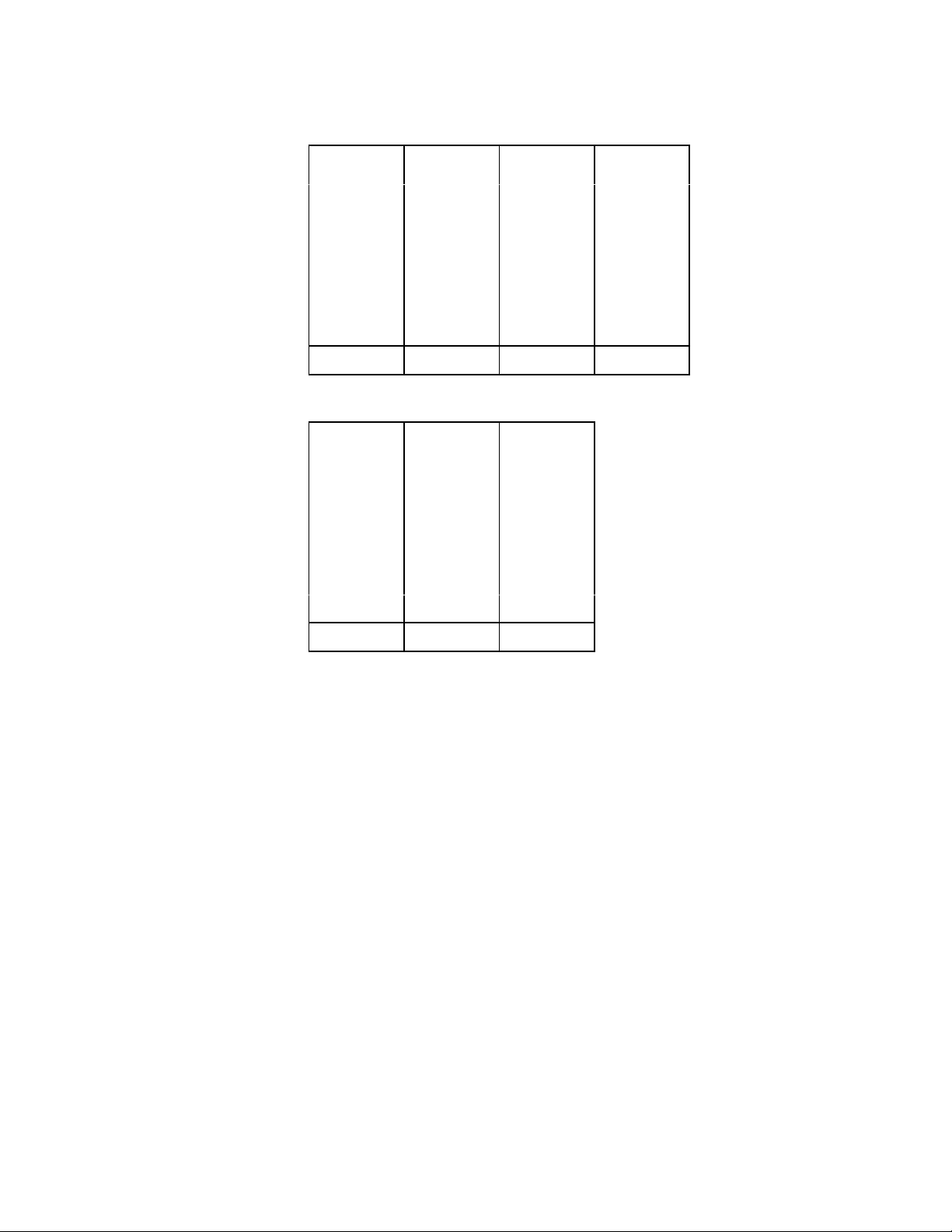
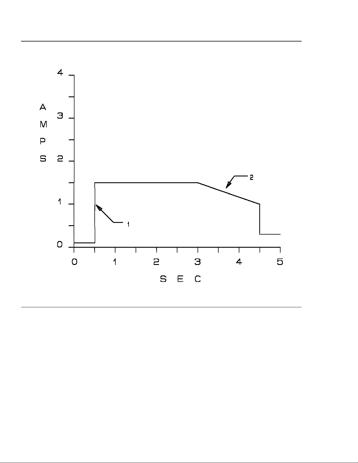
Figure 1. 5 volt current during read/write operations — C1x Models
1. Read/write baseline voltage.
2. Read/write pulse. T he width of the pulse is proportional to the number of consecutive blocks read or
written. The 5 volt supply must be able to provide the required current during this event.
Source filename=POWERIBM CorporationPage 18 of 87
Page 19
USER RESPONSIBLE FOR VERIFYING VERSION AND COMPLETENESS
OEM FUNCTIONAL SPECIFICATION ULTRASTAR XP (DFHC) SSA MODELS 1.12/2.25 GB - 1.0" HIGH
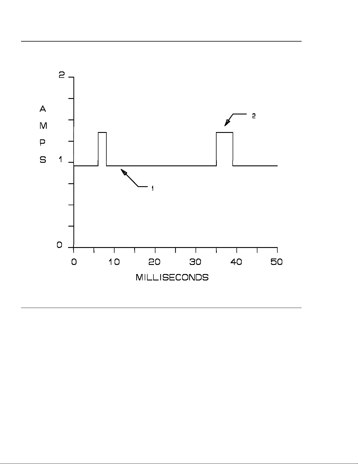
Figure 2. Typical 12 volt current —C1x Models
1. Maximum slew rate is 7 amps/millisecond.
2. Maximum slew rate is 100 amps/millisecond.
3. Maximum slew rate is 7 amps/millisecond.
4. Maximum slew rate is 3 amps/millisecond.
Source filename=POWER IBM Corporation Page 19 of 87
Page 20
USER RESPONSIBLE FOR VERIFYING VERSION AND COMPLETENESS
OEM FUNCTIONAL SPECIFICATION ULTRASTAR XP (DFHC) SSA MODELS 1.12/2.25 GB - 1.0" HIGH
Figure 3. Typical 12 volt spin-up current — C1x Models
1. Maximum slew rate is 20 amps/millisecond.
2. Current drops off as motor comes up t o speed.
Source filename=POWERIBM CorporationPage 20 of 87
Page 21

USER RESPONSIBLE FOR VERIFYING VERSION AND COMPLETENESS
OEM FUNCTIONAL SPECIFICATION ULTRASTAR XP (DFHC) SSA MODELS 1.12/2.25 GB - 1.0" HIGH
2.2.2 C2x Models
The following voltage specifications apply at the drive power connector. There is no special power on/off
sequencing required. T h e extra power needed for Brick O n Sled models an d t he +38V power option are
described in 2.2.4, “CxB Models” on page 33.
Input Voltage
+ 5 Volts Supply 5V (± 5% during r un a n d spin-up)
+1 2 Volts Supply 12V (± 5% during ru n) ( +5 % / -7% during spin-up)
The following current values are the combination measured values of SCSI models an d SSA Cx4 model. T he
differences between SCSI and SSA is + 5V currents. Because of different interface electronics and speed, SSA
electronics card requires more +5 V current than SCSI. Read/Write Base Line is 290 m a higher. Idle
Average is 500 m a higher. (290ma and 500ma differences were found by measuring SSA Cx4 model). SSA
+5V current numbers are derived from SCSI + 5V current numbers by adding 290ma and 500ma accordingly.
Population Population
Power Supply Current Notes Mean Stand. Dev.
+5VDC (power-up) Minimum voltage slew rate = 4.5 V/sec
+5VDC (idle avg) 1.23 Amps 0.02 Amps
+5VDC (R/W baseline) 1.25 Amps
4
0.05 Amps
+5VDC (R/W pulse) Base-to-peak .36 Amps 0.06 Amps
+12VDC (power-up) Minimum voltage slew rate = 7.4 V/sec
+12VDC (idle avg) 0.41 Amps 0.02 Amps
+12VDC (seek avg) 1 op/sec 0.0031 Amps 0.0002 Amps
+12VDC (seek peak) 1.20 Amps
+12VDC (spin-up) 4.2 sec max 1.5 Amps
5
0.02 Amps
6
0.1 Amps
Drive power
Avg idle power 11.07 Watts .35 Watts
Avg R/W power 30 ops/sec 12.25 Watts .35 Watts
4
See Figure 4 on page 24 for a plot of ho w the read/write baseline a n d read/write pulse s um together.
5
Th e idle average a n d seek peek should be added together to determine the total 12 volt peak current. See Figure 5
on page 25 for a typical buildup of these currents. Refer to examples on the following page to see how to combine
these values.
6
The current at start is the total 12 volt current required (ie. the motor start current, module current a nd voice coil
retract current). See Figure 6 o n page 26 for typical 12 volt current during spindle motor start.
Source filename=POWER IBM Corporation Page 21 of 87
Page 22

USER RESPONSIBLE FOR VERIFYING VERSION AND COMPLETENESS
OEM FUNCTIONAL SPECIFICATION ULTRASTAR XP (DFHC) SSA MODELS 1.12/2.25 GB - 1.0" HIGH
2.2.2.1 Power Calculation Examples
Note: The following formulas assume all system ops as a 1 block read or write transfer from a random
cylinder while at nominal voltage condition.
Example 1. Calculate the mean 12 volt average current.
If we assume a case of 30 operations/second then to compute the sum of the 12 volt mean currents the
following is done.
mean
+12VDC (idle average) 0.41 amps
+12VDC (seek average) 0.0031 * 30 = 0.09 amps
TOTAL 0.50 amps
Example 2. Calculate the mean plus 3 sigma 12 volt average current.
To compute the sum of the 12 volt mean current's 1 sigma value assume all the distributions are normal.
Therefore the square root of the sum of the squares calculation applies. Assume a case of 30
operations/second.
sigma
+12VDC (idle average) 0.02 amps
+12VDC (seek average) sqrt(30*((0.0002)**2))= 0.001 amps
TOTAL sqrt((0.02)**2+(.001)**2))=0.02 amps
So the mean plus 3 sigma mean current is 0.50 + 3*0.02 = 0.56 amps
Example 3. Power Calculation.
Nominal idle drive power = (1.23 Amps * 5 Volts) + (0.41 Amps * 12 Volts) = 11.07 Watts
Nominal R /W drive power at 30 ops/sec = (1.25 Amps * 5 Volts) + (0.50 Amps * 12 Volts) = 12.25
Watts
Mean plus 3 sigma drive power for 30 random R/W operations/second. Assume that the 5 volt a nd 12 volt
distributions are independent therefore the square root of the sum of the squares applies.
+5VDC (1 sigma power) 0.05 * 5 = 0.25 watts
+12VDC (1 sigma power) 0.02 * 12 = 0.24 watts
Total (1 sigma power) sqrt((0.25)**2+(0.24)**2) = 0.35 watts
Total power 10.8 + 3 * 0.35 = 11.9 watts
Source filename=POWERIBM CorporationPage 22 of 87
Page 23

USER RESPONSIBLE FOR VERIFYING VERSION AND COMPLETENESS
OEM FUNCTIONAL SPECIFICATION ULTRASTAR XP (DFHC) SSA MODELS 1.12/2.25 GB - 1.0" HIGH
Example 4. Calculate the 12 volt peak current.
To compute the sum of the 12 volt peak currents the following is done.
mean
+12VDC (idle avg) 0.41 amps
+12VDC (seek peak) 1.20 amps
TOTAL 1.61 amps
Example 5. Calculate the mean plus 3 sigma 12 volt peak current.
To compute the sum of the 12 volt peak current's 1 sigma value assume all distributions are normal. Therefore the square root of the sum of the squares calculation applies.
sigma
+12VDC (idle avg) 0.03 amps
+12VDC (seek peak) 0.02 amps
TOTAL sqrt((0.03)**2+(0.02)**2)=0.036 amps
So the mean plus 3 sigma peak current is 1.61 + 3*0.036= 1.72 amps
Things to check when measuring 12 V supply current:
Null the current probe frequently. Be sure to let it warm up.
Adjust the power supply t o 12.00 V at the drive terminals.
Use a proper window width, covering an integral number of spindle revolutions.
Measure values at 25 degree C casting temperature.
Get a reliable trigger for Seek Peak readings.
Source filename=POWER IBM Corporation Page 23 of 87
Page 24
USER RESPONSIBLE FOR VERIFYING VERSION AND COMPLETENESS
OEM FUNCTIONAL SPECIFICATION ULTRASTAR XP (DFHC) SSA MODELS 1.12/2.25 GB - 1.0" HIGH
Figure 4. 5 volt current during read/write operations — C2x Models
1. Read/write baseline voltage.
2. Read/write pulse. T he width of the pulse is proportional to the number of consecutive blocks read or
written. The 5 volt supply must be able to provide the required current during this event.
Source filename=POWERIBM CorporationPage 24 of 87
Page 25
USER RESPONSIBLE FOR VERIFYING VERSION AND COMPLETENESS
OEM FUNCTIONAL SPECIFICATION ULTRASTAR XP (DFHC) SSA MODELS 1.12/2.25 GB - 1.0" HIGH
Figure 5. Typical 12 volt current —C2x Models
1. Maximum slew rate is 7 amps/millisecond.
2. Maximum slew rate is 100 amps/millisecond.
3. Maximum slew rate is 7 amps/millisecond.
4. Maximum slew rate is 3 amps/millisecond.
Source filename=POWER IBM Corporation Page 25 of 87
Page 26
USER RESPONSIBLE FOR VERIFYING VERSION AND COMPLETENESS
OEM FUNCTIONAL SPECIFICATION ULTRASTAR XP (DFHC) SSA MODELS 1.12/2.25 GB - 1.0" HIGH
Figure 6. Typical 12 volt spin-up current — C2x Models
1. Maximum slew rate is 20 amps/millisecond.
2. Current drops off as motor comes up t o speed.
Source filename=POWERIBM CorporationPage 26 of 87
Page 27
USER RESPONSIBLE FOR VERIFYING VERSION AND COMPLETENESS
OEM FUNCTIONAL SPECIFICATION ULTRASTAR XP (DFHC) SSA MODELS 1.12/2.25 GB - 1.0" HIGH
2.2.3 C4x Models
The following voltage specifications apply at the drive power connector. There is no special power on/off
sequencing required. T h e extra power needed for Brick O n Sled models an d t he +38V power option are
described in 2.2.4, “CxB Models” on page 33.
Input Voltage
+ 5 Volts Supply 5V (± 5% during r un a n d spin-up)
+1 2 Volts Supply 12V (± 5% during ru n) ( +5 % / -7% during spin-up)
The following current values are the combination measured values of SCSI models an d SSA Cx4 model. T he
differences between SCSI and SSA is + 5V currents. Because of different interface electronics and speed, SSA
electronics card requires more +5 V current than SCSI. Read/Write Base Line is 290 m a higher. Idle
Average is 500 m a higher. (290ma and 500ma differences were found by measuring SSA Cx4 model). SSA
+5V current numbers are derived from SCSI + 5V current numbers by adding 290ma and 500ma accordingly.
Population Population
Power Supply Current Notes Mean Stand. Dev.
+5VDC (power-up) Minimum voltage slew rate = 4.5 V/sec
+5VDC (idle avg) 1.26 Amps 0.02 Amps
+5VDC (R/W baseline) 1.27 Amps
7
0.05 Amps
+5VDC (R/W pulse) Base-to-peak .36 Amps 0.06 Amps
+12VDC (power-up) Minimum voltage slew rate = 7.4 V/sec
+12VDC (idle avg) 0.77 Amps 0.03 Amps
+12VDC (seek avg) 1 op/sec 0.0036 Amps 0.0002 Amps
+12VDC (seek peak) 1.3 Amps
+12VDC (spin-up) 8.5 sec max 2.2 Amps
8
9
0.02 Amps
0.1 Amps
Drive power
Avg idle power 15.54 Watts .44 Watts
Avg R/W power 30 ops/sec 16.91 Watts .44 Watts
7
See Figure 7 on page 30 for a plot of ho w the read/write baseline a n d read/write pulse s um together.
8
Th e idle average a n d seek peek should be added together to determine the total 12 volt peak current. See Figure 8
on page 31 for a typical buildup of these currents. Refer to examples on the following page to see how to combine
these values.
9
The current at start is the total 12 volt current required (ie. the motor start current, module current a nd voice coil
retract current). See Figure 9 o n page 32 for typical 12 volt current during spindle motor start.
Source filename=POWER IBM Corporation Page 27 of 87
Page 28

USER RESPONSIBLE FOR VERIFYING VERSION AND COMPLETENESS
OEM FUNCTIONAL SPECIFICATION ULTRASTAR XP (DFHC) SSA MODELS 1.12/2.25 GB - 1.0" HIGH
2.2.3.1 Power Calculation Examples
Note: The following formulas assume all system ops as a 1 block read or write transfer from a random
cylinder while at nominal voltage condition.
Example 1. Calculate the mean 12 volt average current.
If we assume a case of 30 operations/second then to compute the sum of the 12 volt mean currents the
following is done.
mean
+12VDC (idle average) 0.77 amps
+12VDC (seek average) 0.0036 * 30 = 0.11 amps
TOTAL 0.88 amps
Example 2. Calculate the mean plus 3 sigma 12 volt average current.
To compute the sum of the 12 volt mean current's 1 sigma value assume all the distributions are normal.
Therefore the square root of the sum of the squares calculation applies. Assume a case of 30
operations/second.
sigma
+12VDC (idle average) 0.02 amps
+12VDC (seek average) sqrt(30*((0.0002)**2))= 0.001 amps
TOTAL sqrt((0.02)**2+(.001)**2))=0.02 amps
So the mean plus 3 sigma mean current is 0.88 + 3*0.02 = 0.94 amps
Example 3. Power Calculation.
Nominal idle drive power = (1.26 Amps * 5 Volts) + (0.77 Amps * 12 Volts) = 15.54 Watts
Nominal R /W drive power at 30 ops/sec = (1.27 Amps * 5 Volts) + (0.88 Amps * 12 Volts) = 16.91
Watts
Mean plus 3 sigma drive power for 30 random R/W operations/second. Assume that the 5 volt a nd 12 volt
distributions are independent therefore the square root of the sum of the squares applies.
+5VDC (1 sigma power) 0.05 * 5 = 0.25 watts
+12VDC (1 sigma power) 0.03 * 12 = 0.36 watts
Total (1 sigma power) sqrt((0.25)**2+(0.36)**2) = 0.44 watts
Total power 15.46 + 3 * 0.44 = 16.8 watts
Source filename=POWERIBM CorporationPage 28 of 87
Page 29

USER RESPONSIBLE FOR VERIFYING VERSION AND COMPLETENESS
OEM FUNCTIONAL SPECIFICATION ULTRASTAR XP (DFHC) SSA MODELS 1.12/2.25 GB - 1.0" HIGH
Example 4. Calculate the 12 volt peak current.
To compute the sum of the 12 volt peak currents the following is done.
mean
+12VDC (idle avg) 0.77 amps
+12VDC (seek peak) 1.3 amps
TOTAL 2.07 amps
Example 5. Calculate the mean plus 3 sigma 12 volt peak current.
To compute the sum of the 12 volt peak current's 1 sigma value assume all distributions are normal. Therefore the square root of the sum of the squares calculation applies.
sigma
+12VDC (idle avg) 0.02 amps
+12VDC (seek peak) 0.02 amps
TOTAL sqrt((0.02)**2+(0.02)**2)=0.028 amps
So the mean plus 3 sigma peak current is 2.07 + 3*0.028= 2.1 amps
Things to check when measuring 12 V supply current:
Null the current probe frequently. Be sure to let it warm up.
Adjust the power supply t o 12.00 V at the drive terminals.
Use a proper window width, covering an integral number of spindle revolutions.
Measure values at 25 degree C casting temperature.
Get a reliable trigger for Seek Peak readings.
Source filename=POWER IBM Corporation Page 29 of 87
Page 30

USER RESPONSIBLE FOR VERIFYING VERSION AND COMPLETENESS
OEM FUNCTIONAL SPECIFICATION ULTRASTAR XP (DFHC) SSA MODELS 1.12/2.25 GB - 1.0" HIGH
Figure 7. 5 volt current during read/write operations — C4x Models
1. Read/write baseline voltage.
2. Read/write pulse. T he width of the pulse is proportional to the number of consecutive blocks read or
written. The 5 volt supply must be able to provide the required current during this event.
Source filename=POWERIBM CorporationPage 30 of 87
Page 31

USER RESPONSIBLE FOR VERIFYING VERSION AND COMPLETENESS
OEM FUNCTIONAL SPECIFICATION ULTRASTAR XP (DFHC) SSA MODELS 1.12/2.25 GB - 1.0" HIGH
Figure 8. Typical 12 volt current —C4x Models
1. Maximum slew rate is 7 amps/millisecond.
2. Maximum slew rate is 100 amps/millisecond.
3. Maximum slew rate is 7 amps/millisecond.
4. Maximum slew rate is 3 amps/millisecond.
Source filename=POWER IBM Corporation Page 31 of 87
Page 32

USER RESPONSIBLE FOR VERIFYING VERSION AND COMPLETENESS
OEM FUNCTIONAL SPECIFICATION ULTRASTAR XP (DFHC) SSA MODELS 1.12/2.25 GB - 1.0" HIGH
Figure 9. Typical 12 volt spin-up current — C4x Models
1. Maximum slew rate is 20 amps/millisecond.
2. Current drops off as motor comes up t o speed.
Source filename=POWERIBM CorporationPage 32 of 87
Page 33

USER RESPONSIBLE FOR VERIFYING VERSION AND COMPLETENESS
OEM FUNCTIONAL SPECIFICATION ULTRASTAR XP (DFHC) SSA MODELS 1.12/2.25 GB - 1.0" HIGH
2.2.4 CxB Models
Th e carrier m od el s include a DC/DC power converter, device activity and fault/service indicators. There is
no additional current required for +5 V or +12V.
2.2.4.1 Power supply methods
When +38V is applied to the interface connector pins +38V Source A, +38V Source B, and Ground, the
+ 38V supply is input to a DC/DC converter that provides +12V and + 5V t o t he drive electronics.
2.2.4.2 DC/DC Converter
Typical efficiency of this converter is 8 0% at maximum output load with input voltage at 38V.
There are tw o independent +38V power supply inputs o n the interface connector which supply two independent inputs to the DC/DC converter, +38V Source A and +38V Source B (refer to Table 12 on
page 65). The DC/DC converter will operate while one input voltage is i n th e range of +3 4V t o + 40V a n d
the other input voltage is in the range of 0 to +40 volts. Input voltage ripple must be less than 1.0 volts
peak-to-peak at the fundamental frequency of 420 H z maximum, less than 500mv at the frequency from
421hz to 1 kh z , less than 100mv at the frequency greater than 1 khz. The converter output is + 5 volts a t
0.3 amps to 2.6 amps and + 12 volts at 0.3 amps to 1.4 amps continuous current. Th e +12v output can
handle a surge current of 2.2 amps in 9 seconds.
The total input current to the converter is 1.6A amps when the highest input voltage on the power supply
input pins is +3 4 volts and t he converter outputs are operating at full load. Th e input current ripple, due to
converter switching is no more than 100 milliamps peak-to-peak at 1 M H z Maximum inrush current is
limited to 3 amps during turn on except for a maximum period of 2 microseconds (during h o t plugging)
where the current can exceed 3 amps bu t is less than 8 amps.
A DC/DC converter output enable is provided on the interface connector. This signal, +DC/DC Enable,is
pulled up within the converter. T o enable the DC outputs, this line must be at or above 2.4 volts. T o
disable t h e DC outputs, the signal must be at or below 1.4 volts.
The DC/DC converter has over-current, over-voltage, an d over-temperature detection. A ny of these conditions will latch off the converter. Th e latch is reset by insuring that both input voltages fall below + 5 volts
for a period greater than o r equal t o 10 milliseconds.
Refer to 5.5, “Option Pins and Indicators” on page 66 for descriptions of the Early Power Off Warning and
Loss of Redundancy fault signals associated wi th th e +3 8V supply inputs.
Source filename=POWER IBM Corporation Page 33 of 87
Page 34

USER RESPONSIBLE FOR VERIFYING VERSION AND COMPLETENESS
OEM FUNCTIONAL SPECIFICATION ULTRASTAR XP (DFHC) SSA MODELS 1.12/2.25 GB - 1.0" HIGH
2.2.5 Power Supply Ripple
Externally Generated Ripple
as seen at drive power connector Maximum Notes
+5VDC 150 mV 0-20 MHz
+12VDC 150 mV 0-20 MHz
During drive start u p a nd seeking, 12 volt ripple is generated by the drive (referred to as dynamic loading). If
several drives have their power daisy chained together then the power supply ripple plus other drive's
dynamic loading must remain within the regulation tolerance window of + /- 5%. A common supply with
separate power leads to each drive is a more desirable method of power distribution.
10
peak-to-peak
peak-to-peak
2.2.6 Grounding Requirements of the Disk Enclosure
Th e disk enclosure is at Power Supply ground potential. I t is allowable for the user mounting scheme to
common the Disk Enclosure to Frame Ground potential or t o leave it isolated from Frame Ground.
From a Electro-Magnetic Compatibility (EMC) standpoint it will, in most cases be preferable to common
the Disk Enclosure to the system's mounting frame. With this in mind, it is important that the Disk Enclosure not become an excessive return current path from the system frame t o power supply. Th e drive's
mounting frame must be within ± 150 millivolts of the drive's power supply ground. At no time should
more than 35 milliamps of current (0 t o 100Mhz) be injected into the disk enclosure.
Please contact your IB M Customer Representative if you have questions o n ho w to integrate this drive in
your system.
2.2.7 Hot plug/unplug support
Power supply and SSA link h ot plug and un-plug is allowed for all SSA models.
For Form Factor models, there is n o special sequence required for connecting 5 volt, 12 volt, or ground.
During a ho t plug-in event the drive being plugged will draw a large amount of current at the instant of
plug-in. This current spike is du e to charging the bypass capacitors o n th e drive. This current pulse may
cause t h e power supply to go out of regulation. If this supply is shared by other drives then a low voltage
power on reset ma y be initiated o n those drives. Therefore the recommendation for ho t plugging is to have
one supply for each drive. Never daisy chain the power leads if hot plugging is planned. H o t plugging
should be minimized to prevent wear o n the power connector.
The carrier models may be hot plugged ONLY IF the ground pins (longer pin) make contact first (before
other pins which are shorter). Vice versa, the carrier m ay be h ot unplugged ONLY IF the ground pins
(longer pins) are the last to remove (after other pins which are shorter). DAMAGE TO THE FILE ELEC-
TRONICS AND THE ADAPTER ELECTRONICS COULD RESULT IF THE ABOVE C OND IT ION S
ARE NO T MET. The mating HP C connector MUST HAVE PROGRAMMABLE PIN LENGTH. GN D
PINS MUST BE LONGER THAN SIGNAL AN D POWER PINS. THE GUIDE PIN S MUST BE TIED
TO THE DOKING ASSEMBLY FRAME GN D
10
This ripple must not cause the power supply to the drive to go outside of the ± 5% regulation tolerance.
Source filename=POWERIBM CorporationPage 34 of 87
Page 35

USER RESPONSIBLE FOR VERIFYING VERSION AND COMPLETENESS
OEM FUNCTIONAL SPECIFICATION ULTRASTAR XP (DFHC) SSA MODELS 1.12/2.25 GB - 1.0" HIGH
Hot plugging t h e SSA link will be recognized by the n e x t node which will cause a configuration process to
be started by the Initiators.
During hot plugging, th e supplies must not go over the upper voltage limit. Th i s means that proper ESD
protection must be used during the plugging event.
During ho t un-plugging if the operating shock limit specification c a n be exceeded then the drive should be
issued a Start/Stop Unit command (spin down) that is allowed t o complete before un-plugging.
Source filename=POWER IBM Corporation Page 35 of 87
Page 36

USER RESPONSIBLE FOR VERIFYING VERSION AND COMPLETENESS
OEM FUNCTIONAL SPECIFICATION ULTRASTAR XP (DFHC) SSA MODELS 1.12/2.25 GB - 1.0" HIGH
2.2.8 Bring-up Sequence (and Stop) Times
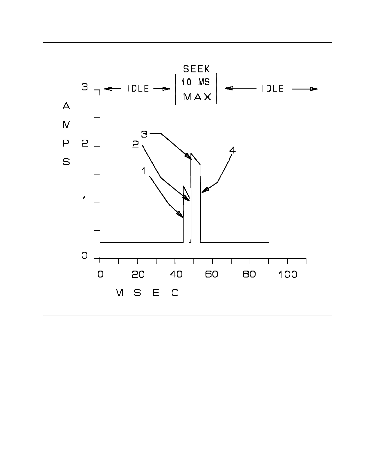
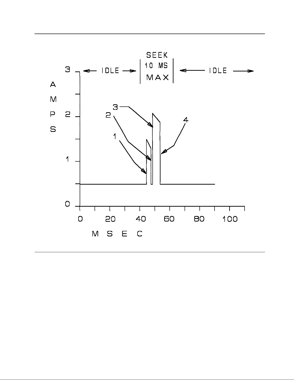
Figure 10. Start Time Diagram
Note: BATS is the abbreviation for Basic Assurance Tests. Start-up sequence spins u p the spindle motor,
initializes the servo subsystem, up-loads code, performs BATS2 (verifies read/write hardware), resumes
"Reassign in Progress" operations, and more. Fo r more information on the start-up sequence, refer to the
Ultrastar XP (DFHC) SS A Models Interface Specification.
Note: If a RESET is issued before th e drive comes ready, the power on sequence will start again. In all
other cases when a RESET is issued the present state of the motor is not altered.
Note: Reference “Start/Stop Unit Time” o n page 49 for additional details.
Note: See 5.7, “Spindle Synchronization” on page 69 for details about Start-up time increases when the
device is requested via Mode Parameters to synchronize the spindle motor to another device.
Event Nominal Maximum Notes
Power-up 1.5 sec 2.0 sec *see Figure 10
Start-up 12.4 sec 45 sec. *see Figure 10
Spin-up 8.2 sec 29.2 sec *see Figure 10
Spindle St o p 6.0 sec 12.0 sec
Table 3. Bring-up Sequence Times a nd Stop Time for C1x Models
Source filename=BRINGUPIBM CorporationPage 36 of 87
Page 37

USER RESPONSIBLE FOR VERIFYING VERSION AND COMPLETENESS
OEM FUNCTIONAL SPECIFICATION ULTRASTAR XP (DFHC) SSA MODELS 1.12/2.25 GB - 1.0" HIGH
Event Nominal Maximum Notes
Power-up 1.5 sec 2.0 sec *see Figure 10
Start-up 17.6 sec 45 sec. *see Figure 10
Spin-up 13.2 sec 29.2 sec *see Figure 10
Spindle St o p 9.0 sec 12.0 sec
Table 4. Bring-up Sequence Times a nd Stop Time for C2x Models
Event Nominal Maximum Notes
Power-up 1.5 sec 2.0 sec *see Figure 10 o n page 36
Start-up 16.5 sec 45 sec. *see Figure 10 on page 36
Spin-up 11.17 sec 30.9 sec *see Figure 10 o n page 36
Spindle St o p 8.0 sec 12.0 sec
Table 5. Bring-up Sequence Times a nd Stop Time for C4x Models
Source filename=BRINGUP IB M Corporation Page 37 of 87
Page 38

USER RESPONSIBLE FOR VERIFYING VERSION AND COMPLETENESS
OEM FUNCTIONAL SPECIFICATION ULTRASTAR XP (DFHC) SSA MODELS 1.12/2.25 GB - 1.0" HIGH
Source filename=PERFORMIBM CorporationPage 38 of 87
Page 39

USER RESPONSIBLE FOR VERIFYING VERSION AND COMPLETENESS
OEM FUNCTIONAL SPECIFICATION ULTRASTAR XP (DFHC) SSA MODELS 1.12/2.25 GB - 1.0" HIGH
3.0 Performance
Drive performance characteristics are dependent upon the workloads ru n and the environments in which
they are run.
All times listed in this chapter are typical values provided for information only, so that the performance for
environments and workloads other than those shown as examples can be approximated. Actual minimum
and maximum values will vary depending upon factors such as workload, logical and physical operating environments.
3.1 Environment Definition
Drive performance criteria is based on the following operating environment. Deviations from this environment may cause deviations from values listed in this specification.
Block lengths are formatted at 512 bytes per block.
The number of data buffer cache segments is 8. The total data buffer length is 512k bytes. Each
segment is of equal length. Therefore, each cache segment is 64k bytes.
The number of blocks of customer data that can fit into one segment is reduced because 2 bytes of L RC
information is also stored in th e segment for each block of customer data stored in the segment. Therefore, use t he following equation to determine how many blocks c an fit into one segment.
512KB
(
# of segments
ub/lba +2
Ten byte Read and Write commands are used.
SSA environment consists of a single initiator and single target with no SSA link contention.
The Initiator delay in responding t o messages from the Target is assumed to be zero.
All performance enhancing functions are disabled, except where noted. More specifically,
− Comman ds are no t queued
− Caching is disabled (RCD=1, WCE=0)
− Out of order transfers are not allowed (OOTM=0, OOTI=0)
The media is formatted with th e skew definition that optimizes the disk d a ta transfer rate for unsynchronized spindle operation.
All Current Mode Parameters are set to their Default values except where noted.
Averages are based on a sample size of 10,000 operations.
)
3.2 Workload Definition
Th e drive's performance criteria is based on the following command workloads. Deviations from these
workloads m ay cause deviations from this specification.
Operations are either all Reads or all Writes. The specifications for Command Execution Time with
Read Ahead describe exceptions to this restriction. F or that scenario all commands are preceded by a
Read command, except for sequential write commands.
The Data Transfer size is set to 64 Blocks.
Source filename=PERFORM IBM Corporation Page 39 of 87
Page 40

USER RESPONSIBLE FOR VERIFYING VERSION AND COMPLETENESS
OEM FUNCTIONAL SPECIFICATION ULTRASTAR XP (DFHC) SSA MODELS 1.12/2.25 GB - 1.0" HIGH
The time between the end of a n operation, and when the next operation is issued is 50 msec, +/ - a
random value of 0 to 50 msec, unless otherwise noted.
3.2.1 Sequential
N o Seeks. The target LBA for all operations is the previous L B A + 64.
3.2.2 Random
All operations are to random LBAs. The average seek is an average weighted seek.
3.3 Command Execution Time
Command execution, or service, times are th e su m of several Basic Components:
1. Seek
2. Latency
3. Command Execution Overhead
4. Data Transfer to/from Disk
5. Data Transfer to/from SSA Link
The impact or contribution of those Basic Components to Command Execution Time is a function of the
workload being sent to the drive a nd the environment in which the drive is being operated.
3.3.1 Basic Component Descriptions
Seek
The average time from the initiation of the seek, to the acknowledgement that the R/ W head is
on the track that contains the first requested L B A . Values are population averages, a nd vary as
a function of operating conditions. T h e values used t o determine Command Execution Times
for sequential commands is 0 milliseconds and th e values for random commands are shown in
section 2.0, “Specifications” on page 11.
Latency
The average time required from the activation of the read/write hardware until the target sector
has rotated to the head and the read/write begins. This time is 1/2 of a revolution of the disk, or
4.17 milliseconds.
Command Execution Overhead
The average time added to the Command Execution Time due to the processing of t he
command. It includes all ti m e the drive spends not doing a disk operation or SSA link data
transfer.
The following values are used whe n calculating the Command Execution Times.
Workload Command Execution
Sequential Read .65 ms
Sequential Write 1.00 ms
Random Read .25 ms
Random Write .30 ms
Table 6. Overhead Values
A number of Initiator controlled factors affect Command Execution Overhead. These are examined separately in 3.4, “Approximating Performance for Different Environments” on page 43.
Source filename=PERFORMIBM CorporationPage 40 of 87
Page 41

USER RESPONSIBLE FOR VERIFYING VERSION AND COMPLETENESS
OEM FUNCTIONAL SPECIFICATION ULTRASTAR XP (DFHC) SSA MODELS 1.12/2.25 GB - 1.0" HIGH
The Post Command Processing time of .26 ms is defined as the average time required for process
cleanup after the command has completed. If a re-instruct period faster tha n this time is used, the
difference is added t o th e Command Execution Overhead of the next operation.
Data Transfer to/from Disk
The average time used t o transfer th e data between th e media and t he drive's internal data buffer.
This is calculated from:
(Data Transferred)/(Media Transfer Rate).
There are four interpretations of Media Transfer Rate. H ow it is to be used helps decide which
interpretation is appropriate t o use.
1. Instantaneous Data Transfer Rate
The same for a given notch formatted at any of the supported logical block lengths. I t varies
by notch only and does no t include any overhead.
2. Track Data Sector Transfer Rate
Varies depending upon the formatted logical block length and varies from notch t o notch. It
includes t h e overhead associated with each individual sector. This is calculated from:
(user bytes/sector)/(individual sector time)
(Contact an IBM Customer Representative for individual sector times of the various for-
matted block lengths.)
3. Theoretical Data Sector Transfer Rate
Also includes t im e required for track and cylinder skew and overhead associated with each
track. (See 3.3.2.1, “Theoretical Data Sector Transfer Rate” on page 43 for a description on
how to calculate it.)
4. Typical Data Sector Transfer Rates
Also includes th e effects of defective sectors and skipped revolutions due to error recovery.
See Appendix B of the Ultrastar XP (DFHC) SSA Models Interface Specification for a
description of error recovery procedures.
Rates for drives formatted at 512 bytes/block are located in Table 7 on page 42.
Source filename=PERFORM IBM Corporation Page 41 of 87
Page 42

USER RESPONSIBLE FOR VERIFYING VERSION AND COMPLETENESS
OEM FUNCTIONAL SPECIFICATION ULTRASTAR XP (DFHC) SSA MODELS 1.12/2.25 GB - 1.0" HIGH
Model Type All C4x C2x C1x
Notch # Instant. Track Theoretical Typical Theoretical Typical Theoretical Typical
Average 12.07 7.91 7.17 7.13 7.13 7.10 7.06 7.03
1 12.58 8.30 7.52 7.48 7.48 7.44 7.40 7.37
2 12.58 8.30 7.52 7.48 7.48 7.44 7.40 7.37
3 12.51 7.99 7.22 7.18 7.18 7.15 7.11 7.08
4 11.96 7.74 7.02 6.99 6.99 6.95 6.92 6.89
5 11.26 7.38 6.66 6.63 6.63 6.60 6.57 6.54
6 11.05 7.07 6.41 6.38 6.38 6.35 6.31 6.28
7 10.64 6.88 6.23 6.20 6.19 6.16 6.13 6.10
8 10.29 6.64 6.03 6.00 6.00 5.97 5.94 5.91
9 10.01 6.45 5.85 5.83 5.83 5.80 5.77 5.74
10 9.59 6.15 5.55 5.53 5.53 5.50 5.48 5.45
Note: The values for Typical Data Sector Transfer Rates assume a typically worst case value of 3.16 errors in 109bits read at
nominal conditions for soft error rate.
Note: Contact an IBM Customer Representative for values when formatted at other block lengths.
Note: "Average" values a re sums of the individual notch values weighted by the number of LBAs in the associated notches.
Table 7. Data Sector Transfer Rates. (All rates are in MB/sec)
Data Transfer to/from SSA Link
The time required to transfer data between the SSA link an d the drive's internal dat a buffer, that
is n o t overlapped with t he time for the Seek, Latency or Data Transfer to/from Disk.
When the drive is reading, data is transferred from the medium to its data buffer an d from the
buffer across the SSA link simultaneously. However, data transfer t o the link from the data
buffer buffer lags transfer from the medium t o the buffer b y one block. At the e nd of the transfer
from the medium, one block still has to be transferred across the link.
For a write operation, the data is normally transferred t o the d at a buffer during the seek and
latency time. In the rare case that these are both zero, the write cannot begin until one sector is
transferred, a n d th e ti me t o do this becomes part of the overhead.
Each block of data is transferred as one or more frames on the SSA Link. Each frame requires
10 bytes of overhead and may contain up t o 128 bytes of data. The time to transfer one block
depends on the number of frames required. For example, a 744 byte block needs 6 frames (5 x
128 byte, 1 x 10⁴). T his adds 60 bytes of overhead making 804 bytes total. At an instantaneous
transfer rate of 20MB/s, that is 40 microseconds per block (17.7MB/s sustained).
3.3.2 Comments
Overlap has been removed from the Command Execution Time calculations. The components of the
Command Execution Times are truly additive times to the entire operation. Fo r example,
The Post Command Processing times are n o t components of the Command Execution time therefore
they are not included in the calculation of environments where the re-instruct period exceeds the Post
Command Processing time.
The effects of idle time functions are not included in the above examples. The 3.2.1, “Sequential” o n
page 40 and 3.2.2, “Random” on page 40 bot h define environments where the effects due to increased
command overhead of Idle Time Functions upon Command Execution time are less than 0.15%.
Source filename=PERFORMIBM CorporationPage 42 of 87
Page 43

USER RESPONSIBLE FOR VERIFYING VERSION AND COMPLETENESS
OEM FUNCTIONAL SPECIFICATION ULTRASTAR XP (DFHC) SSA MODELS 1.12/2.25 GB - 1.0" HIGH
3.3.2.1 Theoretical Data Sector Transfer Rate
This Rate does no t account for time required for error recovery or defective sectors (the Typical Data Sector
Transfer Rate described in 3.3.1, “Basic Component Descriptions” on page 40 does include those effects).
Each group of cylinders with a different number of gross sectors per track is called a notch. Th e following
shows values for notch #1 of C4x models. Th e "Average" values used in this specification are sums of the
individual notch values weighted b y the number of LBAs in the associated notches. Fo r the other notches
and block lengths use values that correspond to those notches and block lengths.
Data Sector Transfer Rate =
Bytes/cylinder
time for 1 cyl+ track skews + 1 cyl skew
Bytes/cylinder = {(tracks/cyl)(gross sectors/track) - spares/cyl}(user bytes/sector)
= {(16)(135) - 40}(512)
= 1,085,440 Bytes/cyl
time for 1 cyl of data = {(tracks/cyl)(gross sectors/track) - spares/cyl}(avg. sector time)
= {(16)(135) - 40}(.061705)
= 130.815 msec/cyl
time for track skews = (tracks/cyl - 1)(track skew)(avg. sector time)
= (16-1)(13)(.061700)
= 12.032 msec/cyl
time for 1 cyl skew = (cylinder skew)(avg. sector time)
= (25)(.061705)
= 1.543 msec/cyl
Data Sector Transfer Rate =
1,085,440 Bytes
130.815 msec + 12.032 msec + 1.543 msec
= 7.517 MB/sec (Notch #1)
Note: See 2.0, “Specifications” on page 11 for the descriptions of
tracks/cyl (trk/cyl)
gross sectors/track (gs/trk)
spares/cyl (b1spr/cyl an d b2spr/cyl)
user bytes/sector (ub/sct)
gross bytes/sector (gb/sct)
See 3.5, “Skew” o n page 46 for the descriptions of
track skew (tss)
cylinder skew (css)
Average sector times per notch can be calculated as follows:
average sector time (ast) =
1 sec
120.045 × gs/trk
3.4 Approximating Performance for Different Environments
Source filename=PERFORM IBM Corporation Page 43 of 87
Page 44

USER RESPONSIBLE FOR VERIFYING VERSION AND COMPLETENESS
OEM FUNCTIONAL SPECIFICATION ULTRASTAR XP (DFHC) SSA MODELS 1.12/2.25 GB - 1.0" HIGH
3.4.1 For Different Transfer Sizes
The primary performance change due to a change of transfer size is the Data Transfer to/from Disk parameter. See 3.3.1, “Basic Component Descriptions” on page 40 for an explanation of the calculation of this
parameter.
The Command Execution Overhead m ay also change if the transfer size is reduced to the point where certain
internal control functions can n o longer be overlapped with either t he SSA Link or Disk data transfer.
For example, a short read may incur u p t o .65ms extra overhead if t he Data Ready/Reply exchange does not
overlap th e disk transfer.
3.4.2 When Read Caching i s Enabled
For read commands with Read Caching Enabled Command Execution time can be approximated by
deleting Seek, Latency, and Data Transfer to/from Disk components if all of the requested data is available
in a cache segment (cache hit). Command Execution Overhead increases by approximately .1ms in this case
as there is n o overlap with seek/latency.
When some, bu t n o t all, of the requested data is available in a cache segment (partial cache hit) Data
Transfer to/from Disk will be reduced b u t n ot eliminated. Seek and Latency may or may n o t be reduced
depending upon the location of requested data not in the cache and location of the read/write heads at the
time the command was received.
The contribution of the Data Transfer to/from SSA link to the Command Execution time may increase since
a larger, or entire, portion of the transfer may no longer be overlapped with the components that were
reduced.
3.4.3 When Write Caching i s Enabled
For write commands with th e Write Caching Enabled (WCE) Mode parameter bit set, Command Execution
time can be approximated by deleting Seek, Latency, and Data Transfer to/from Disk components. The
contribution of the Data Transfer to/from SSA link to th e Command Execution time may increase since a
larger, or entire, portion of the transfer may no longer be overlapped with the components that were
reduced. T h e reduced times effectively are added to the Post Command Processing Time.
Command completion status is returned when data is completely stored in the buffer. T he time to transfer
this group of data to the disk will be added to the performance of any next command that was in the queue.
3.4.4 When Adaptive Caching is Enabled
The Adaptive Caching feature attempts to increase Read Cache hit ratios by monitoring workload and
adjusting cache control parameters, normally determined by the using system via th e Mode Parameters, with
algorithms using the collected workload information.
3.4.5 When Read-ahead is Enabled
If read-ahead is active, th e service tim e is affected i n several ways:
If the data requested by a read command is all in the data buffer already, t h e command can be serviced
very quickly.
If th e beginning of the requested dat a is in t he buffer, an d the read-ahead is still in progress, data transfer
Source filename=PERFORMIBM CorporationPage 44 of 87
Page 45

USER RESPONSIBLE FOR VERIFYING VERSION AND COMPLETENESS
OEM FUNCTIONAL SPECIFICATION ULTRASTAR XP (DFHC) SSA MODELS 1.12/2.25 GB - 1.0" HIGH
for the command can start immediately. This effectively avoids latency tim e for read operations sequential on a previous read.
If the data requested by a read operation is not in the read-ahead buffers, there is an increase in t h e
command overhead time due to the time spent searching t h e buffers. This time depends o n the number
of buffer segments selected by the Mode Select command.
If read-ahead is still in progress whe n the next command is received and th e data requested is not
sequential, the drive aborts read-ahead and starts the command. T he time t o perform this abort
increases t he Command Execution Overhead by .23ms.
3.4.6 When No Seek is Required
For a Read command, the additional Command Execution Overhead when no seek is required is approximately .50ms. For a Write, it is approximately .70ms.
3.4.7 For Queued Commands
If commands are sent t o the drive wh en it is busy performing a previous command, they can be queued. I n
this case, some of the command processing is performed during the previous command and the overhead for
the queued command is reduced by approximately .20 milliseconds.
3.4.7.1 Reordered Commands
If the Queue Algorithm Modifier Mode Parameter field is set to allow it, commands in the device command
queue may be executed in a different order than they were received. Commands are reordered so that the
seek portion of Command Execution time is minimized. The amount of reduction is a function of the
location of the 1st requested block per command and the rate at which t he commands are sent to th e drive.
A Queue Algorithm Modifier Mode Parameter value of 9 enables an algorithm that gives the using system
the ability t o place ne w commands into the drive command queue execution order relative to t h e outstanding commands in the queue. For example, if a request is sent to the drive that the using system prioritizes such that it's completion time is more important than one or more of the outstanding commands, the
using system can increase the likelihood that command is executed before those others by using a tag value
greater than those outstanding commands.
3.4.7.2 Back-To-Back Commands
If consecutive read/write commands access contiguous data, they can be serviced without incurring disk
latency between commands.
Note: There is a minimum transfer length for a given environment where continuous access to t he disk can
not be maintained without missing a motor revolution. For Write commands with Write Caching enabled
the likelihood is increased that shorter transfers c a n fulfill the requirements needed to maintain continuous
writing to the disk.
Back-to-back Read is only enabled if Read-ahead is disabled.
3.4.8 Out of Order Transfers
Tw o bits in th e SCSI Command message control out of order transfers. OOTM applies to transfers to/from
the media a nd OOTI applies to transfers to/from the interface (SSA Link).
Th e benefit from setting OOTM increases as t h e transfer length approaches o ne disk revolution. This affects
both reads an d writes and is du e to the reduction in latency.
Source filename=PERFORM IBM Corporation Page 45 of 87
Page 46

USER RESPONSIBLE FOR VERIFYING VERSION AND COMPLETENESS
OEM FUNCTIONAL SPECIFICATION ULTRASTAR XP (DFHC) SSA MODELS 1.12/2.25 GB - 1.0" HIGH
The full benefit of o ut of order transfers in only achieved if OOTI is also set. Read data is transferred on the
interface in t h e same order as it was read from the media.
3.5 Skew
3.5.1 Cylinder to Cylinder Skew
Cylinder skew is the s um of the sectors required for physically moving the heads (csms), which is a function
of the formatted block length and recording density (notch #), and reassign allowance sectors (ras = 3) used
to maintain optimum performance over t he normal life of the drive.
Note: The values in t h e Mode Page 3 'Cylinder Skew Factor' are notch specific non-synchronized spindle
mode values. The value for notch 1 is returned when the Active Notch is set to 0.
Notch #
User bytes / logical
block
256 42 42 42 40 38 36 36 36 36 32
512 28 28 27 26 25 24 24 23 22 21
520 26 26 26 26 24 24 23 22 22 21
522 26 26 26 25 24 24 23 22 22 20
524 26 26 26 25 24 24 23 22 22 20
528 26 26 26 25 24 24 23 22 22 20
600 24 24 24 23 22 22 21 20 20 20
688 22 22 22 21 20 20 20 20 18 18
744 21 21 21 20 20 20 18 18 17 17
Note: Contact an IBM Customer Representative for values at other formatted block lengths.
Table 8. Optimal Cylinder Skew for several block lengths
1 2 3 4 5 6 7 8 9 10
In order to increase th e likelihood that equivalent LBA's on two or more devices are located at the same
relative physical position when the devices ar e used in a synchronized spindle mode, cylinder skew is calculated differently. The cylinder skew calculations d o n o t take into account known defective sites. To prohibit
revolutions from being missed on cylinder crossings by drives formatted while i n a synchronized spindle
mode, an extra allowance for 6 defects is added that is not added when optimally formatted in a nonsynchronized mode.
3.5.2 Track t o Track Skew
Note: The values in t h e SCSI Mode Page 3 'Track Skew Factor' are notch specific values. The value for
notch 1 is returned when the Active Notch is set to 0.
Source filename=PERFORMIBM CorporationPage 46 of 87
Page 47

USER RESPONSIBLE FOR VERIFYING VERSION AND COMPLETENESS
OEM FUNCTIONAL SPECIFICATION ULTRASTAR XP (DFHC) SSA MODELS 1.12/2.25 GB - 1.0" HIGH
Notch #
User bytes / logical
block
256 20 20 20 19 19 17 17 17 17 15
512 13 13 13 12 12 11 11 10 10 10
520 12 12 12 12 11 11 10 10 10 10
522 12 12 12 12 11 11 10 10 10 9
524 12 12 12 12 11 11 10 10 10 9
528 12 12 12 12 11 11 10 10 10 9
600 11 11 11 11 10 10 10 9 9 9
688 10 10 10 10 9 9 9 9 8 8
744 9 9 9 9 9 9 8 8 8 7
Note: Contact an IBM Customer Representative for values at other formatted block lengths.
Table 9. Track (or Head) Skew f or several block lengths
1 2 3 4 5 6 7 8 9 10
3.6 Idle Time Functions
The execution of various functions by the drive during idle times may result in delays of commands
requested by initiators. ‘Idle time’ is defined as time spent by the drive n ot executing a command requested
by a initiator. Th e functions performed during idle time are:
1. Servo R un Out Measurements
2. Servo Bias Measurements
3. Predictive Failure Analysis (PFA)
4. Channel Calibration
5. Save Logs a nd Pointers
6. Disk Sweep
The command execution time for commands received while performing idle time activities may be increased
by the amount of time it takes t o complete the idle time activity. The messages and d a t a exchanged across
the SSA link are no t affected by idle time activities.
Note: Command Timeout Limits do no t change d ue to idle time functions.
All Idle Time Functions have mechanisms to lessen performance impacts for critical response time periods of
operation. And in some cases virtually eliminate those impacts from an Initiator's point of view. All Idle
Time Functions will only be started if the drive has not received a SCSI command for at least 5 seconds (40
seconds for Sweep). This means that multiple SCSI commands are accepted and executed without delay if
the commands are received b y the drive within 5 seconds after the completion of a previous SCSI command.
This mechanism has the benefit of n ot requiring special system software (such as issuing SCSI Rezero U nit
commands at known & fixed time intervals) in order to control if and when this function executes.
Note: Applications which can only accommodate Idle Time Function delays at certain times, bu t can no t
guarantee a 5 second re-instruction period, may consider synchronizing idle activities to the system needs
through use of the LITF bit in Mode Select Page 0, a n d the Rezero Unit command. Refer to the Ultrastar
XP (DFHC) S SA Models Interface Specification for more details
Following are descriptions of th e various types of idle functions, ho w often they execute a n d their duration.
Duration is defined to be t he maximum amount of time the activity c a n add to a command when n o errors
occur. No more than one idle function will be interleaved with each command.
Following th e descriptions is a summary of the possible impacts to performance.
Source filename=PERFORM IBM Corporation Page 47 of 87
Page 48

USER RESPONSIBLE FOR VERIFYING VERSION AND COMPLETENESS
OEM FUNCTIONAL SPECIFICATION ULTRASTAR XP (DFHC) SSA MODELS 1.12/2.25 GB - 1.0" HIGH
3.6.1 Servo Run Out Measurements
The drive periodically measures servo run out, the amount of wobble o n each disk, t o track follow more
precisely.
Servo run out for all heads is measured every 60 minutes, therefore th e frequency of r u n out measurements is
dependent on the number of heads a particular model has. Th e drive attempts to spread t he measurements
evenly in time and each measurement takes 100 milliseconds. For example, a model C4x with 8 heads performs o ne r u n o u t measurement every 7 1/2 minutes (60 / 8).
3.6.2 Servo Bias Measurements
The drive periodically measures servo bias, the amount of resistance to head movement as a function of disk
radius. It also helps prevent disk lubrication migration by moving t he heads over th e entire disk surface.
Servo bias is measured every 12 minutes during the first hour after a power cycle, and every 60 minutes after
that. The measurement takes 200 milliseconds.
3.6.3 Predictive Failure Analysis
Predictive Failure Analysis measures drive parameters an d can predict if a drive failure is imminent.
Eight different PFA measurements are taken for each head. All measurements for all heads are taken over a
period of 4 hours, therefore the frequency of PF A is dependent on the number of heads a particular model
has. The drive attempts to spread the measurements evenly in ti m e an d each measurement takes about 80
milliseconds. For example, a C4x model with 8 heads will perform on e P F A measurement every 3.7
minutes (240 / 8 × 8). Fo r the last head tested for a particular measurement type (once every 1/ 2 hour), the
data is analyzed and stored. The extra execution time for those occurrences is approximately 40 milliseconds.
This measurement/analysis feature can be disabled for critical response time periods of operation by setting
the Page 0h Mode Parameter LITF = 1. The using system also ha s the option of forcing execution at
known times by issuing the Rezero Uni t command if the Page 0h Mode Parameter TCC = 1. All tests for
all heads occur at those times.
Note: Refer t o the Ultrastar X P (DFHC) SS A Models Interface Specification for more details about PFA,
LITF, and TCC.
3.6.4 Channel Calibration
The drive periodically calibrates the channel to insure that the read a nd write circuits function optimally,
thus reducing the likelihood of soft errors.
Channel calibration is done once every 4 hours and typically completes in 20 milliseconds, but may take up
to 64 milliseconds p er measurement.
The measurement will only be started if the drive has not received a command for at least 5 seconds. Th i s
means that multiple commands are accepted a n d executed without delay if th e commands are received by the
drive within 5 seconds after the completion of a previous command. This function also makes use of the
mechanism t o alter t h e idle detection period to limit execution for critical response time periods of operation,
if needed.
Source filename=PERFORMIBM CorporationPage 48 of 87
Page 49

USER RESPONSIBLE FOR VERIFYING VERSION AND COMPLETENESS
OEM FUNCTIONAL SPECIFICATION ULTRASTAR XP (DFHC) SSA MODELS 1.12/2.25 GB - 1.0" HIGH
3.6.5 Save Logs and Pointers
The drive periodically saves data in logs in the reserved area of the disks. Th e information is used by the
drive to support various commands and for the purpose of failure analysis.
Logs are saved every 35 minutes. The amount of time it takes to update the logs varies depending o n th e
number of errors since the last update. In most cases, updating those logs and th e pointers to those logs will
occur in less than 30 milliseconds.
3.6.6 Disk Sweep
The heads are moved to another area of the disk if the drive has not received a command for at least 40
seconds. After flying in the same spot for 9 minutes, the heads are moved t o another position. Execution
time is less than 1 full stroke seek.
3.6.7 Summary
Idle Time Function Type Max. Frequency of Occurrence
(minutes)
Servo Run Out 60/(trk/cyl) 100 Re-instruction Period
Servo Bias ( < 1st hour) 12 200 Re-instruction Period
Servo Bias ( > 1st hour) 60 200 Re-instruction Period
PFA 30/(trk/cyl) 80 Re-instruction Period / LITF
Channel Calibration 240 64 Re-instruction Period
Save Logs & Pointers 35 30 Re-instruction Period
Note: "Re-instruction Period" is the time between consecutive SCSI command requests.
Table 10. Summary of Idle Time Function Performance Impacts
Duration (ms) Mechanism to Delay/Disable
3.7 Command Timeout Limits
The 'Command Timeout Limit' is defined as th e time period from w hen the SCSI_command message is
received b y the drive until the corresponding SCSI_status message is transmitted by the drive.
Th e following times are for environments where Automatic Reallocation is disabled and there are n o queued
commands.
Reassignment Time:
Blocks" command.
The drive sh ould be allowed a minimum of 45 seconds to complete a "Reassign
Format Time:
The time to complete a "Format Unit" command (with Immed bit = 0) varies by model:
C4x 45 minutes
C2x 25 minutes
C1x 15 minutes
Initiators should also use this time to allow format sequences initiated by "Format Unit" commands (with
Immed bit = 1) to compete and place the drive in a "ready for use" state.
Start/Stop Unit Time:
The drive sho u l d b e allowed a minimum of 30 seconds t o complete a "Start/Stop
Unit" command (with Immed bit = 0).
Initiators should also use this ti me t o allow start-up sequences initiated by au t o start u ps a n d "Start/Stop
Unit" commands (with Immed bit = 1) to complete and place th e drive in a "ready for use" state.
Source filename=PERFORM IBM Corporation Page 49 of 87
Page 50

USER RESPONSIBLE FOR VERIFYING VERSION AND COMPLETENESS
OEM FUNCTIONAL SPECIFICATION ULTRASTAR XP (DFHC) SSA MODELS 1.12/2.25 GB - 1.0" HIGH
Note: A timeout of one minute or more is recommended but N O T required. T h e larger system timeout
limit allows the system to tak e advantage of the extensive ERP/DRP that the drive may attempt in order to
successfully complete the start-up sequence.
Note: A 60 second minimum is required if electronics card replacement is required as a service practice.
Please contact an IB M Customer Representative for more details if required.
Medium Access Command Time:
The timeout limit for medium access commands that transfer user data
and/or non-user data should be a minimum of 30 seconds. These commands are:
Log Select
Log Sense
Mode Select
Mode Sense
Pre-Fetch
Read
Read Capacity
Read Defect Data
Read Long
Receive Diagnostic Results
Release
Reserve
Rezero Un it
Seek
Send Diagnostic
Verify
Write
Write a nd Verify
Write Buffer
Write Long
Write Sam e
Note: The 30 sec limit assumes the absence of SSA link contention and user data transfers of 64 blocks or
less. This time sho uld be adjusted for anticipated SSA link contention and if longer user d at a transfers are
requested.
Timeout limits for other commands:
The drive s h o u l d be allowed a minimum of 5 seconds to complete
these commands:
Format Unit (with Immed bit = 1)
Inquiry
Read Buffer
Read Memory
Request Sense
Start/Stop Un it (with Immed bit = 1)
Synchronize Cache
Test Uni t Ready
When Automatic Reallocation is enabled add 45 seconds t o the timeout of the following commands: Read
(6), Read (10), Write (6), Write (10), Write an d Verify, and Write Same.
The command timeout for a command that is not located at th e head of the command queue should be
increased b y the sum of command timeouts for all of the commands that are performed before it is.
Source filename=PERFORMIBM CorporationPage 50 of 87
Page 51

USER RESPONSIBLE FOR VERIFYING VERSION AND COMPLETENESS
OEM FUNCTIONAL SPECIFICATION ULTRASTAR XP (DFHC) SSA MODELS 1.12/2.25 GB - 1.0" HIGH
4.0 Mechanical
4.1 Small Form Factor Models (CxC)
4.1.1 Weight and Dimensions
C1C & C2C Models C4C Models
U.S. S.I. Metric U.S. S.I. Metric
Weight 1.00 pounds 0.46 kilograms 1.80 pounds 0.82 kilograms
Height 1.00 inches 25.4 millimeters 1.63 inches 41.3 millimeters
Width 4.00 inches 101.6 millimeters 4.00 inches 101.6 millimeters
Depth 5.75 inches 146.0 millimeters 5.75 inches 146.0 millimeters
4.1.2 Clearances
A minimum of 2 mm clearance sh o u l d be given to the bottom surface except for a 10 mm maximum diameter area around the bottom mounting holes. Figure 11 and Figure 12 show the clearance requirements
(Note 1). Fo r proper cooling it is suggested that a clearance of 6 mm be provided under the drive a nd on
top of the drive.
There should be 7 m m of clearance between drive's that are mounted with their t o p sides (see Figure 22 o n
page 78 for top view of drive) facing each other.
4.1.3 Mounting
The drive can b e mounted with any surface facing down.
The drive is available with both side and bottom mounting holes. Refer t o Figure 11 t o Figure 13 for the
location of these mounting holes for each configuration.
The maximum allowable penetration of the mounting screws is 3.8 m m.
The torque applied t o t he mounting screws must be 0.8 Newton-meters ± 0.1 Newton-meters.
The recommended torque t o be applied t o t he mounting screw is 0.8 Newton-meter ± 0.4 Newton-meter.
IBM will provide technical support to users that wish t o investigate higher mounting torques in their application.
WARNING: The drive may be sensitive to user mounting implementation due to frame distortion effects.
IBM will provide technical support to assist users to overcome mounting sensitivity.
Source filename=MECHANIC IBM Corporation Page 51 of 87
Page 52

USER RESPONSIBLE FOR VERIFYING VERSION AND COMPLETENESS
OEM FUNCTIONAL SPECIFICATION ULTRASTAR XP (DFHC) SSA MODELS 1.12/2.25 GB - 1.0" HIGH
notes: 1) Bottom clearance required by 4.1.2, “Clearances.”
2) Dimensions are in millimeters.
Figure 11. Location of Side Mounting Holes of C1C & C2C Models
Source filename=MECHANICIBM CorporationPage 52 of 87
Page 53

USER RESPONSIBLE FOR VERIFYING VERSION AND COMPLETENESS
OEM FUNCTIONAL SPECIFICATION ULTRASTAR XP (DFHC) SSA MODELS 1.12/2.25 GB - 1.0" HIGH
notes: 1) Bottom clearance required by 4.1.2, “Clearances” on page 51.
2) Dimensions are in millimeters.
Figure 12. Location of Side Mounting Holes of C4C Models
Source filename=MECHANIC IBM Corporation Page 53 of 87
Page 54

USER RESPONSIBLE FOR VERIFYING VERSION AND COMPLETENESS
OEM FUNCTIONAL SPECIFICATION ULTRASTAR XP (DFHC) SSA MODELS 1.12/2.25 GB - 1.0" HIGH
notes:
1) T he purpose of this drawing is to show the bottom hole pattern.
2) Dimensions are in millimeters.
Figure 13. Location of Bottom Mounting Holes of CxC Models
Source filename=MECHANICIBM CorporationPage 54 of 87
Page 55

USER RESPONSIBLE FOR VERIFYING VERSION AND COMPLETENESS
OEM FUNCTIONAL SPECIFICATION ULTRASTAR XP (DFHC) SSA MODELS 1.12/2.25 GB - 1.0" HIGH
4.1.4 Unitized Connector Locations
The Unitized connector is located on t he left side of the top view (bottom drawing) as shown in Figure 14
on page 56. T he jumper connector is located o n the right side of th e to p view (bottom drawing) as shown
in Figure 14 on page 56. This jumper connector is referred to as Front Jumper because of its front
location. I t is reserved for I BM Engineering used only.
Source filename=MECHANIC IBM Corporation Page 55 of 87
Page 56

USER RESPONSIBLE FOR VERIFYING VERSION AND COMPLETENESS
OEM FUNCTIONAL SPECIFICATION ULTRASTAR XP (DFHC) SSA MODELS 1.12/2.25 GB - 1.0" HIGH
Figure 14. Electrical connectors (rear an d top view) -- CxC Models.
Source filename=MECHANICIBM CorporationPage 56 of 87
Page 57

USER RESPONSIBLE FOR VERIFYING VERSION AND COMPLETENESS
OEM FUNCTIONAL SPECIFICATION ULTRASTAR XP (DFHC) SSA MODELS 1.12/2.25 GB - 1.0" HIGH
4.2 Carrier Models (CxB)
The carrier model assemblies include the disk drive, drawer mounting hardware (rails, latching mechanism,
and connector), a nd DC/DC power converter.
4.2.1 Weight and Dimensions
C1B & C2B Models C4B Models
U.S. S.I. Metric U.S. S.I. Metric
Weight 2.00 pounds 0.92 kilograms 2.80 pounds 1.288 kilograms
Height 1.75 inches 44.5 millimeters 1.75 inches 44.5 millimeters
Width 4.26 inches 108.3 millimeters 4.26 inches 108.3 millimeters
Depth 10.72 inches 272.3 millimeters 10.72 inches 272.3 millimeters
Refer t o Figure 15 o n page 58 for detailed dimensions.
4.2.2 Clearances
For proper cooling, a clearance of 6 millimeters s ho u ld b e provided above and below the carrier surfaces.
Adequate airflow is needed in order t o meet the operating specifications. Maximum temperatures are specified for critical drive components in Table 15 on page 78.
4.2.3 Mounting
The drive can b e mounted with any surface facing down.
The carrier is designed to be plugged into a n auto-docking assembly. The auto-docking assembly contains
an electrical receptacle that provides connections for DC power, SSA interface signals, an d fault sensing and
reporting signals (see 5.2, “Carrier Connector” on page 64). The carrier design allows for positive retention
of t h e carrier in all axes whe n plugged into the auto-docking assembly. I n addition, the carrier retention
provides a force to bottom out the carrier auto-docking connector into the auto-docking assembly an d maintain a force of 5 pounds minimum, 40 pounds maximum.
The mating connector should contain two guide pins to align the carrier receptacle during seating. These
guide pins are BERG part number 77693-014 (IBM part number 72G0343) or AM P equivalent part number
1-532808-1 (IBM part number 19G6789). Th e guide pi n length shoul d be 26.04 millimeters while th e t h r e a d
depth depends upon the thickness of t he circuit board the connector is mounted to. The guide pins sh ould
be tied t o the docking assembly frame ground.
Note: The connector pins must be lubricated t o insure seating of the carrier into the auto-docking assembly.
The type of lubricant recommended is Stauffer CL-920 or equivalent.
WARNING: The drive may be sensitive to user mounting implementation due to frame distortion effects.
IBM will provide technical support to assist users to overcome mounting sensitivity.
Source filename=MECHANIC IBM Corporation Page 57 of 87
Page 58

USER RESPONSIBLE FOR VERIFYING VERSION AND COMPLETENESS
OEM FUNCTIONAL SPECIFICATION ULTRASTAR XP (DFHC) SSA MODELS 1.12/2.25 GB - 1.0" HIGH
Note: Dimensions are in millimeters.
Figure 15. Dimensions —CxB Models
Source filename=MECHANICIBM CorporationPage 58 of 87
Page 59

USER RESPONSIBLE FOR VERIFYING VERSION AND COMPLETENESS
OEM FUNCTIONAL SPECIFICATION ULTRASTAR XP (DFHC) SSA MODELS 1.12/2.25 GB - 1.0" HIGH
Figure 16. Handle Docking and Ejection System
The handle on the carrier is used for insertion into and extraction from the drawer. It also provides enough
force to ensure seating of the carrier electrical receptacle with the mating connector. Referring to Figure 16,
with the handle in the STOP or open position, a carrier inserted into the auto-docking assembly will have
the connector guide pins inserted into the carrier receptacle but th e connector pins will not be making
contact with the carrier receptacle. Moving the carrier handle to the C A M IN position and eventually to the
LOCKED position sets the auto-docking connector with the carrier receptacle and holds the carrier i n all the
mounting positions listed above. Moving the handle from the LOCKED position to the EJECT position
provides leverage via the c am surface on t he handle acting against th e side rails to separate the connector
pins from the receptacle.
Source filename=MECHANIC IBM Corporation Page 59 of 87
Page 60

USER RESPONSIBLE FOR VERIFYING VERSION AND COMPLETENESS
OEM FUNCTIONAL SPECIFICATION ULTRASTAR XP (DFHC) SSA MODELS 1.12/2.25 GB - 1.0" HIGH
4.2.4 Auto-docking Assembly Side Rails
IBM supplied side rails that can be used for the auto-docking assembly are shown in Figure 17 on page 61
along with mounting location information. Refer to the figure for the following notes:
Note 1: With the side rails mounted within the given tolerances, there will be a nominal 1.5 millimeter
interference between the handle and side rail to provide positive retention of the carrier an d the
handle.
Note 2: Th e IB M part number of the auto-docking side rails is 36G6422.
Source filename=MECHANICIBM CorporationPage 60 of 87
Page 61

USER RESPONSIBLE FOR VERIFYING VERSION AND COMPLETENESS
OEM FUNCTIONAL SPECIFICATION ULTRASTAR XP (DFHC) SSA MODELS 1.12/2.25 GB - 1.0" HIGH
Figure 17. Side Rail Positioning
Source filename=MECHANIC IBM Corporation Page 61 of 87
Page 62

USER RESPONSIBLE FOR VERIFYING VERSION AND COMPLETENESS
OEM FUNCTIONAL SPECIFICATION ULTRASTAR XP (DFHC) SSA MODELS 1.12/2.25 GB - 1.0" HIGH
4.2.5 Electrical Connector and Indicator Locations
The HPC electrical connectors are located as shown in Figure 15 o n page 58. The indicators (LEDs) are
located as shown in Figure 18 o n page 62.
Figure 18. LE D Locations (front view) —CxB Models.
Source filename=MECHANICIBM CorporationPage 62 of 87
Page 63

USER RESPONSIBLE FOR VERIFYING VERSION AND COMPLETENESS
OEM FUNCTIONAL SPECIFICATION ULTRASTAR XP (DFHC) SSA MODELS 1.12/2.25 GB - 1.0" HIGH
5.0 Electrical Interface
5.1 SS A Unitized Connector
Electrical connections for Cx C models are provided by a single connector mounted o n the rear of the drive
(see Figure 14 o n page 56). Connections are provided for tw o SSA ports, fault sensors and indicators,
option customization, and power. Refer t o Figure 19 an d Table 11 o n page 64 for contact assignments.
Figure 19. Unitized Connector (looking in the file at the connector end)
Source filename=ELECTRIC IBM Corporation Page 63 of 87
Page 64

USER RESPONSIBLE FOR VERIFYING VERSION AND COMPLETENESS
OEM FUNCTIONAL SPECIFICATION ULTRASTAR XP (DFHC) SSA MODELS 1.12/2.25 GB - 1.0" HIGH
Pin SSA PORT SSA PORT OPTION PORT POWER PORT
1 + Line O ut + Line Out - MTM + 12V Charge
(long)
2 - Line O u t - Line Ou t - Auto Start + 5V Charge (long)
3 Gnd (long) Gn d (long) - Sync Gn d (long)
4 Gn d (long) Gnd (long) - Write Protect + 12V
5 - Line I n - Line In Gn d (long) + 12V
6 + Line I n + Line In - Device Activity + 12V
7 N/A N/A +5V Gnd (long)
8 N/A N/A - Device Fault Gnd (long)
9 N/A N/A Programmable 1 +5V
10 N/A N/A Programmable 2 +5V
11 N/A N/A N/A - Power Fail
12 N/A N/A N/A G ND (long)
13 N/A N/A N/A + 3.3V
14 N/A N/A N/A + 3.3V
15 N/A N/A N/A Gn d (long)
16 N/A N/A N/A Gn d (long)
Table 11. Electrical Connector Contact Assignments — C x C Models
5.2 Carrier Connector
Electrical connections for Cx B models are provided by a single 128 pin connector mounted o n the rear of
the drive (see Figure 15 o n page 58 for lo ca t io n) . Connections are provided for t wo SSA ports, fault
sensors a nd indicators, an d power. Th e receptacle used is a 4×32, female contact, BERG HPC connector,
IBM part number 99F9429. Refer t o Figure 20 an d Table 12 o n page 65 for contact assignments.
Figure 20. Carrier Interface Receptacle
Source filename=ELECTRICIBM CorporationPage 64 of 87
Page 65

USER RESPONSIBLE FOR VERIFYING VERSION AND COMPLETENESS
OEM FUNCTIONAL SPECIFICATION ULTRASTAR XP (DFHC) SSA MODELS 1.12/2.25 GB - 1.0" HIGH
Row A B C D
1 n/c n/c n/c n/c
2 n/c n/c n/c n/c
3 n/c n/c n/c n/c
4 n/c n/c n/c n/c
5 n/c n/c n/c n/c
6 n/c n/c n/c n/c
7 n/c n/c n/c Device Fault (*)
8 +38V Source A +38V Source A +38V Source A + 38V Source A
9 +38V Source A +38V Source A +38V Source A + 38V Source A
10 Ground Ground Ground Ground
11 Ground Ground Ground Ground
12 +38V Source B +38V Source B +38V Source B +38V Source B
13 +38V Source B +38V Source B +38V Source B +38V Source B
14 n/c n/c n/c n/c
15 n/c n/c n/c n/c
16 n/c n/c n/c n/c
17 Shield Shield Shield Shield
18 + Out 1 + Out 1 +In2 +In2
19 − Out 1 − Out 1 − In 2 − In 2
20 Shield Shield Shield Shield
21 +In1 +In1 + Out 2 + Out 2
22 − In 1 − In 1 − Out 2 − Out 2
23 Shield Shield Shield Shield
24 n/c n/c n/c n/c
25 n/c n/c n/c n/c
26 n/c n/c n/c n/c
27 n/c n/c n/c n/c
28 n/c n/c n/c n/c
29 n/c n/c n/c n/c
30 n/c n/c n/c n/c
31 n/c n/c n/c n/c
32 n/c n/c n/c n/c
Note:
"n/c" means "no connection" (not used).
(*) means pin is reserved for this function bu t model CxB does no t provide connection t o support it.
Table 12. Electrical Connector Contact Assignments — C xB Models
Source filename=ELECTRIC IBM Corporation Page 65 of 87
Page 66

USER RESPONSIBLE FOR VERIFYING VERSION AND COMPLETENESS
OEM FUNCTIONAL SPECIFICATION ULTRASTAR XP (DFHC) SSA MODELS 1.12/2.25 GB - 1.0" HIGH
5.3 SSA Link Cable
Th e SSA link cable must meet the specifications described in t h e Electrical Specifications section of Serial
Storage Architecture SSA-PH (Transport Layer), X3T10.1/94-015 rev 01.
5.4 SSA Link Electrical Characteristics
The drive S S A link line driver, line receiver, and line receiver termination are fully compliant with the specifications described in the Electrical Specifications section of Serial Storage Architecture SSA-PH (Transport
Layer), X3T10.1/94-015 rev 01.
5.5 Option Pins and Indicators
Ultrastar XP SSA drives contain option pins and/or indicators used to sense and report fault conditions, and
to enable certain features of the drive. The electrical characteristics and requirements of these pins are fully
compliant with the specifications described in the Electrical Specification section of Serial Storage Architec-
ture SSA-PH (Transport Layer), X3T10.1/989D rev 01. The existence a n d definition of these pins are model
dependent. Refer to Figure 14 on page 56 an d Figure 18 o n page 62 for locations of pins a n d LEDs on
the front of the drive. Refer to Table 11 o n page 64 and Table 12 on page 65 for locations of pins o n t he
rear of t he drive.
5.5.1 - Manufacturing Test Mode (Option Port Pin 1)
A low active input pin, that when active (pulled below .8V) makes pins 2, 3, 4, 6, 8 ,9 and 10 available t o
be redefined. Pins 5 a nd 7 must remain Ground and +5V respectively. On e possible purpose for this p in is
to allow a manufacturing tester t o redefine th e option pins to whatever functions it desires, while allowing
the shipped product to return to the standard definitions in the customers environment. All models (CxC
and CxB) reserve this pin b u t it is n o t connected t o any internal logic.
5.5.2 - Auto Start Pin (Option Port Pin 2)
A low active input pin, that when active (pulled below 0.8 V) o n C x C model causes the drive motor to spin
up and become ready for media access operations after power is applied without the need to receive a
Start/Stop Unit command. When inactive (pulled above 2.0 V), the drive motor shall not spin up until after
the receipt of a Start/Stop Unit command. The signal is to be sampled by the device at power on, or hard
reset o r soft reset conditions. Refer to the "Option Pins" section of the Ultrastar XP (DFHC) SS A Models
Interface Specification for a detailed functional description of operations associated with this pin.
This pin is not accessible on CxB models.
5.5.3 - Sync Pin (Option Port Pin 3)
The Sync input/output pin on CxC model can be used for synchronizing among devices. The synchronization is achieved by having on e device use s this pin as output to transmit o ne sync character once per its
spindle revolution. Th e other node may use this pi n as a n input and synchronize their spindle revolution
position t o match the Sync signal. The SSA network provide Sync character over SSA link, b u t this option
pin allows synchronization across multiple SSA networks, or allow tighter latency of th e Sync pulse. Refer t o
Figure 21 o n page 70 for examples of Synchronization connection.
Source filename=ELECTRICIBM CorporationPage 66 of 87
Page 67

USER RESPONSIBLE FOR VERIFYING VERSION AND COMPLETENESS
OEM FUNCTIONAL SPECIFICATION ULTRASTAR XP (DFHC) SSA MODELS 1.12/2.25 GB - 1.0" HIGH
The width, period, a nd tolerance of t he negative active Sync pulse is manufacturer dependent, and thus synchronization across different manufacturers or even different product lines of the same manufacturer is n ot
guaranteed. T h e Sync pi n usage is con t rolled by mod e pages within the mode select command.
This pin is not accessible on CxB model.
5.5.4 - Write Protect (Option Port Pin 4)
a low active input pin, that when active (pulled below 0.8 V), the drive will prohibit commands that alter t h e
customer data area portion of the the media from being performed. T h e state of this pin is monitored on a
per command basis. Refer to "Option pins" section of the Ultrastar X P (DFHC) S SA Models Interface
Specification for a detailed functional description of this pin.
This pin is not accessible on CxB models.
5.5.5 - Ground long (Option Port Pin 5)
The Ground long output pin o n CxC and CxB models shall be capable of syncing 1.0 Amp of current. This
pin is longer than any others in the option block t o allow for t h e ground to mate first or last in a hot-plug or
hot-unplug situation.
5.5.6 - Device Activity Pin/Indicator (Option Port Pin 6)
A low active LE D output pin on CxC models can be used to drive an external Light Emitting Diode. CxB
models have a n integrated Green LED . Refer to the "Option Pins" section of the Ultrastar X P (DFHC)
S SA Models Interface Specification for a detailed func tion al description of this pin/LED.
CxC models provide up to 24 mA of TT L level LED sink current capability. Current limiting for t he LED
is provided on the electronics card. The anode may be tied to the +5 V power source (provided on the th e
unitized connector). Th e LED Cathode is then connected t o the Device Activity pin t o complete the circuit.
5.5.7 + 5V (Option Port Pin 7)
The +5Voutput pin on CxC and CxB models shall supply up to 1.0 A m p of current limited + 5 V (+/-
10%), as long as power is supplied to the device.
5.5.8 - Device Fault Pin/Indicator (Option Port Pin 8)
The Device Fault pin on CxC models can be used t o drive a n external Light Emitting Diode. CxB models
have a n integrated Amber LED . Refer to t he "Option Pins" section of the Ultrastar X P (DFHC) SS A
Models Interface Specification for a detailed functional description of this pin/LED.
CxC models provide up to 24 mA of TT L level LED sink current capability. Current limiting for t he LED
is provided on the electronics card. The anode may be tied to the +5 V power source (provided on the th e
unitized connector). Th e LED Cathode is then connected t o the Device Fault pin t o complete the circuit.
Source filename=ELECTRIC IBM Corporation Page 67 of 87
Page 68

USER RESPONSIBLE FOR VERIFYING VERSION AND COMPLETENESS
OEM FUNCTIONAL SPECIFICATION ULTRASTAR XP (DFHC) SSA MODELS 1.12/2.25 GB - 1.0" HIGH
5.5.9 Programmable pin 1 (Option Port Pin 9)
This pin can be used by a manufacturer for what ever purposes it desires within th e specified definition,
electrical characteristic and th e availability of microcode. This pin is completely controlled by microcode.
Refer t o the "Option Pins" section of the Ultrastar XP (DFHC) S SA Models Interface Specification for a
detailed functional description of this pin.
This pins is no t accessible externally on CxB models.
5.5.10 Programmable pin 2 (Option Port Pin 10)
Thi s pin is reserved and i t is not connected to any internal logic.
This pins is no t accessible externally on CxB models.
5.5.11 - Early Power Off Warning or Power Fail (Power Port Pin 11)
The Early Power Off Warning input pin on CxC models can be used t o indicate to th e drive that a power
loss will occur by pulling this signal to ground. T he input must provide a minimum of 6 milliseconds
warning before power falls below operating specifications in order for the drive to stop its activities and
handle the fault. Refer t o t he "Option Pins" section of the Ultrastar XP (DFHC) SSA Models Interface
Specification for a detailed functional description of t he fault handling associated w ith this pin..
This pin is not accessible on CxB models.
5.5.12 12V Charge and 5V Charge (Power Port pin 1 and 2)
These pins are longer th a n the others. They help t o reduce current spikes during h ot plug. Each pin require a
resistor (not in the drive) in series between the power source a nd t he drive connector. This allows for more
controlled current draw as prior to other voltage pins. I t is up to the subsystem to determine the proper
resistance t o add to these pins to meet the + /- 1 0 % voltage drop limitations an d the current draw limitation
of the connector.
These pins are no t accessible on C xB mod els
5.6 Front Jumper Connector
All models contain a jumper block (refer to Figure 14 o n page 56) that is reserved for I BM Engineering use
only.
Source filename=ELECTRICIBM CorporationPage 68 of 87
Page 69

USER RESPONSIBLE FOR VERIFYING VERSION AND COMPLETENESS
OEM FUNCTIONAL SPECIFICATION ULTRASTAR XP (DFHC) SSA MODELS 1.12/2.25 GB - 1.0" HIGH
5.7 Spindle Synchronization
5.7.1 Synchronization overview
Spindle synchronization of drives is achieved b y one node transmitting a special Sync character or a Sync
pulse once per every revolution of its drive. The transmitting is done either o n SSA Link (sending Sync
character) o r o n a hard-wire (Sending Sync pulse) that connects all th e drives via t he S S A Option Port
'Sync' pin. The synchronization mo de is controlled by the RP L field of the Mode Select Page 04h parameter
(see Ultrastar XP (DFHC) SSA Models Interface Specification for more details). The drive can operate in
one of three modes:
5.7.2 Synchronization Mode
Mode Operation
No Sync Spindle synchronization is disabled.
Slave Sync Spindle synchronization is attempted by synchronizing the spindle motor to the Sync
special character o n SSA link (or th e Sync pulse on Sync hard-wire) that is driven by
another node.
Master Sync Spindle synchronization is no t attempted by this device. It generates a Sync special
character via SSA link (or a Sync pulse via a hard-wire) once per its spindle revolution.
Master Sync Control Master Sync Control is not supported.
5.7.3 Synchronization time
It will take 6 seconds t o synchronize the Slave drive to the Master drive. While the Slave drive is synchronizing t o these characters, it is n ot able to read or write data. Once synchronized the drive will maintain ±
20 microseconds synchronization tolerance.
When operating in Slave Sync mode, the drive must receive the Spindle Sync special characters a t a period of
8.333 milliseconds with a tolerance of ± .025% (2.08 microseconds).
5.7.4 Synchronization with Offset
The Rotational Offset value is th e amount of rotational skew that the Target uses when synchronized. The
rotational skew is applied in t he retarded direction (lagging the synchronized spindle master control). Th e
value in th e field is the numerator of a fractional multiplier that has 256 as its denominator (e.g., a value of
128 indicates a one-half revolution skew). A value of 00h indicates that rotational offset is no t used. Th e
rotational offset is only used when the Drive is running in the Slave Sync R PL mode.
5.7.5 Synchronization Route
5.7.5.1 Over SSA Link
Spindle Sync special characters are forwarded from one SSA link t o the other with a delay of 350
nanoseconds with a tolerance of ± 50 nanoseconds. This delay ca n b e increased by 50 nanoseconds when
the drive is sending the second of a double character sequence (R R or ACK) and by 50 nanoseconds when
sending a S AT or SAT' character.
Source filename=SYNC IBM Corporation Page 69 of 87
Page 70

USER RESPONSIBLE FOR VERIFYING VERSION AND COMPLETENESS
OEM FUNCTIONAL SPECIFICATION ULTRASTAR XP (DFHC) SSA MODELS 1.12/2.25 GB - 1.0" HIGH
Th e spindle synchronization timing requirements are met in a string composed of Ultrastar XP SSA drives
when there are n o more tha n seventeen drives between the o ne operating in Master Sync mo d e a n d t he
furthest drive operating in Slave Sync mode.
5.7.5.2 Over Sync Hard-wire
There will be a single wire that connects all t he drives together throught the SSA Option Port pin 3 (- Sync
pin). O n e of these drives will be a Master drive. Two potential configurations of this hard-wire connection
are shown in the following figures:
Figure 21. Two examples of Daisy-Chain Connection of Synchronization .
Source filename=SYNCIBM CorporationPage 70 of 87
Page 71

USER RESPONSIBLE FOR VERIFYING VERSION AND COMPLETENESS
OEM FUNCTIONAL SPECIFICATION ULTRASTAR XP (DFHC) SSA MODELS 1.12/2.25 GB - 1.0" HIGH
Termination
Bus termination of the - SYNC signals is internal to the drive. This signal has a 5.1K o h m pulled-up to
the + 5 volt supply. A maximum of 30 drives can have their - SYNC line daisy chained together. Violating this could damage the Master drive line driver o n the - SYNC line
It is the using system's responsibility t o provide the cable to connect the - SYNC line where needed, of
the synchronized drives.
Bus Characteristics
− maximum Bus length = 6 meters
− 2 micro-second negative active pulse (when sourced by drive)
− minimum of 1 micro-second negative active pulse w h e n externally sourced
− 0.8 volts = valid lo w input
− 2.2 volts = valid hig h input
− 0.4 volts = low output
− Vcc volts = High output
− 30 milli-amps = maximum output low level sink current
The driver used for these t w o signal lines is a Open Drain buffer.
Source filename=SYNC IBM Corporation Page 71 of 87
Page 72

USER RESPONSIBLE FOR VERIFYING VERSION AND COMPLETENESS
OEM FUNCTIONAL SPECIFICATION ULTRASTAR XP (DFHC) SSA MODELS 1.12/2.25 GB - 1.0" HIGH
Source filename=RELIABLEIBM CorporationPage 72 of 87
Page 73

USER RESPONSIBLE FOR VERIFYING VERSION AND COMPLETENESS
OEM FUNCTIONAL SPECIFICATION ULTRASTAR XP (DFHC) SSA MODELS 1.12/2.25 GB - 1.0" HIGH
6.0 Reliability
Note: The reliability projections are based o n t he conditions stated below. All of the SSA models will meet
the projections as long as reliability operating conditions are no t exceeded.
6.1 Error Detection
Error reporting ≥ 99% All detected errors excluding interface a n d BATs #1 (Basic Assur-
ance Test) errors
Error detection ≥ 99%
FRU isolation = 100% To the device when the "Recommended Initiator Error Recovery
Procedures" in the Ultrastar XP (DFHC) SSA Models Interface
Specification are followed.
No isolation t o sub-assemblies within the device are specified.
6.2 Data Reliability
Probability of not recovering data 10 i n 1015bits read
Recoverable read errors 10 in 1013bits read (measured at nominal DC conditions and room
environment with default error recovery —QPE**)
Probability of miscorrecting unrecoverable data
Note: Eighteen bytes of ECC and two bytes of LR C are provided for each d ata block.
6.3 Seek Error Rate
The drives ar e designed t o have less than 10 errors in 10,000,000 seeks. In th e field, a seek error rate of 40 in
100, 000 seeks will trip P FA (Predictive Failure Analysis) error.
The drives are designed t o achieve Soft Seek Error rate of 1 error in 100,000,000 seeks.
6.4 Power On Hours Examples:
Maximum power on hours (with minimum power on/off cycles)
43,800 hours for life based on:
- 5 Power on/off cycles per month
- 730 power on hours per month
Nominal power on hours (with nominal power on/off cycles)
30,000 hours for life based on:
**
Refer to Ultrastar XP (DFHC) SSA Models Interface Specification for t he definition of QP E (Qualify Post Error).
Source filename=RELIABLE IB M Corporation Page 73 of 87
Page 74

USER RESPONSIBLE FOR VERIFYING VERSION AND COMPLETENESS
OEM FUNCTIONAL SPECIFICATION ULTRASTAR XP (DFHC) SSA MODELS 1.12/2.25 GB - 1.0" HIGH
- 25 Power on/off cycles per month
- 500 power on hours per month
6.5 Power on/off cycles
Maximum on/off cycles 1080/ year
6.6 Useful Life
Product Life 5 Years
Useful life is the length of time prior to the point at which product degradation begins to occur. The specification for the useful life calculation is the same as that for the *MTBF specification.
Source filename=POHIBM CorporationPage 74 of 87
Page 75

USER RESPONSIBLE FOR VERIFYING VERSION AND COMPLETENESS
OEM FUNCTIONAL SPECIFICATION ULTRASTAR XP (DFHC) SSA MODELS 1.12/2.25 GB - 1.0" HIGH
6.7 *Mean Time Between Failure (*MTBF)
The mean time t o failure targe t is 1,000,000 device hours per fail (3.0% CDF) based o n the following
assumptions:
6000 power on hours per year (500 power on hours per month times 12 months)
300 average on/off cycles per year (25 power cycles per month times 12 months)
Seeking/Reading/Writing is assumed to be 20% of power on hours (Approximately 10 read/write operations per second)
Operating at or below the Reliability temperature specifications (See Table 15 on page 78) an d nominal
voltages (See 2.2, “Power Requirements by Model” on page 15)
Note: *MTBF - is a measure of the failure characteristics over total product life. *MTBF includes normal
integration induced, installation, early life (latent), and intrinsic failures. *MTBF is predicated on supplier
qualification, product design verification test, a n d field performance data.
6.7.1 Sample Failure Rate Projections
Th e following tables are for reference only. Th e tables contain failure rate projections for a given set of user
conditions. Similar projections will be provided, upon request, for each user specific power o n hour and
power cycles per month condition. Contact your I B M customer representative for a customized projection.
Application Electronics only - (RA/MM)
1st 30
days
500POH/MM 0.00120 0.0010 0.00096 0.00036 2.1%
730POH/MM 0.00160 0.00140 0.00125 0.00047 2.8%
Table 13. Projected failure rates for the electronics only.
Application Electronics and HDA - (RA/MM)
1st 30
days
500POH/MM 0.00150 0.00130 0.00120 0.00050 3.0%
730POH/MM 0.00200 0.00170 0.00160 0.00070 4.1%
Table 14. Projected failure rates for the entire drive. (Electronics and HDA).
1st 60
1st 60
days
days
1st 90
1st 90
days
days
30 day
average
30 day
average
over
over
life
life
CDF
CDF
6.8 SPQL (Shipped product quality level)
LA vintage Ultimate (13th month)
Targets .25% .10%
6.9 Install Defect Free
Source filename=POH IBM Corporation Page 75 of 87
Page 76

USER RESPONSIBLE FOR VERIFYING VERSION AND COMPLETENESS
OEM FUNCTIONAL SPECIFICATION ULTRASTAR XP (DFHC) SSA MODELS 1.12/2.25 GB - 1.0" HIGH
Install Defect Free percentage 99.99 percent
6.10 Periodic Maintenance
No n e required
6.11 ESD Protection
The Ultrastar XP SSA disk drives contain electrical components sensitive to damage due t o electrostatic
discharge ( ESD) . Proper E SD procedures must be followed during handling, installation, a nd removal. This
includes t h e use of ESD wrist straps a nd ESD protective shipping containers.
6.12 Connector Insertion Cycles
Live insertion and removal of th e electrical connector causes pitting o n the connector terminals. Because of
this th e number of live insertion and removal cycles must be limited.
Maximum Insertion/Removal Cycles (for hot and normal insertion) 25
Source filename=POHIBM CorporationPage 76 of 87
Page 77

USER RESPONSIBLE FOR VERIFYING VERSION AND COMPLETENESS
OEM FUNCTIONAL SPECIFICATION ULTRASTAR XP (DFHC) SSA MODELS 1.12/2.25 GB - 1.0" HIGH
7.0 Operating Limits
The IB M Corporate specifications a n d bulletins, such as C-S 1-9700-000 in the contaminants section, that
are referenced in this document are available for review. (Please contact your IB M Customer)
7.1 Environmental
Temperature
Operating Ambient 41 to 131˚F (5 t o 55˚C)
Operating Casting Temperature 41 to 158˚F (5 to 70˚C)
Storage 34 to 149˚F (1 to 65˚C) See Note
Shipping - 4 0 to 149˚F (-40 to 65˚C)
Temperature Gradient
Operating 36˚F (20˚C) per hour
Shipping and storage below condensation
Humidity
Operating 5 % to 9 0 % noncondensing
Storage 5% to 9 5 % noncondensing
Shipping 5 % to 100% (Applies at th e packaged level)
Wet Bulb Temperature
Operating 80˚F (26.7˚C) maximum
Shipping and Storage 85˚F (29.4˚C) maximum
Elevation
Operating and Storage -1000 to 10,000 feet (-304.8 to 3048 meters)
Shipping -1000 to 40,000 feet (-304.8 to 12,192 meters)
Note: Guidelines for storage below 1˚ C are given i n IBM Technical Report T R 07.2112.
7.1.1 Temperature Measurement Points
The following is a list of measurement points an d their temperatures (maximum and reliability). Maximum
temperatures must not be exceeded at t he worst case drive and system operating conditions with the drive
randomly seeking, reading an d writing. Reliability temperatures must not be exceeded at t he nominal drive
and system operating conditions with the drive randomly seeking, reading, and writing.
There must be significant air flow through the drive s o that the casting an d module temperature limits define
in Table 15 are no t exceeded. Figure 22 o n page 78 defines where measurements should be made to determine the to p casting temperature during drive operation. Figure 23 on page 79 identify the module
locations o n t he bottom side of the card and t h e measurement location o n the bottom of the casting.
Source filename=OPLIMITS IBM Corporation Page 77 of 87
Page 78

USER RESPONSIBLE FOR VERIFYING VERSION AND COMPLETENESS
OEM FUNCTIONAL SPECIFICATION ULTRASTAR XP (DFHC) SSA MODELS 1.12/2.25 GB - 1.0" HIGH
Table 15. Maximum and Reliability Operating Temperature Limits
Maximum Reliability
Disk Enclosure Top 158˚F (70˚C) 131˚ F (55˚C)
Disk Enclosure Bottom 158˚F (70˚ C) 131˚F (55˚ C)
PRDF Prime Module 203˚F (95˚C) 176˚ F (80˚C)
W D 61C40 Modul e 185˚F (85˚C) 167˚ F (75˚c)
SIC Module 203˚F (95˚ C) 176˚F (80˚ C)
Microprocessor Mo dul e 194˚F (90˚C) 167˚F (75˚C)
VCM FE T 194˚F (90˚ C) 167˚F (75˚ C)
DC/DC Converter (CxB only) 185˚F (85˚C) 167˚F (75˚C)
SMP F ET 194˚F (90˚C) 167˚F (75˚C)
Note 1: Modu le temperature measurements should be taken from the to p surface of the module.
Note 2: If copper tape is used t o attach temperature sensors, it sh ou l d be n o larger than 6 square milli-
meters.
notes: 1) dimensions are in millimeters.
Figure 22. Temperature Measurement Points for All Models (top view of DE)
Source filename=OPLIMITSIBM CorporationPage 78 of 87
Page 79

USER RESPONSIBLE FOR VERIFYING VERSION AND COMPLETENESS
OEM FUNCTIONAL SPECIFICATION ULTRASTAR XP (DFHC) SSA MODELS 1.12/2.25 GB - 1.0" HIGH
Notes: 1) Center thermocouple on the top surface of th e module.
2) If copper tape is used t o attach temperature sensors, it s hould be no
larger tha n 6 mm square.
3) Dimensions are in millimeters.
4) The connector (on the left edge) does n o t represent SSA connector.
Figure 23. Temperature Measurement Points for all Models (bottom view)
7.2 Vibration and Shock
The operating vibration and shock limits in this specification are verified in two mount configurations for
CxC models:
1. By mounting with the 6-32 bottom holes with t he drive o n 2 m m clearance as required by 4.1.2,
“Clearances” o n page 51
2. By mounting o n any two opposing pairs of t he 6-32 side mount holes.
CxB models are mounted rigidly to the test fixture using the carrier guides, connector, and latch mechanism.
Th e test fixture is then mounted to the vibration table (the test fixture must not have any resonance within
the frequencies tested).
Other mount configurations may result in different operating vibration a nd shock performance.
Source filename=OPLIMITS IBM Corporation Page 79 of 87
Page 80

USER RESPONSIBLE FOR VERIFYING VERSION AND COMPLETENESS
OEM FUNCTIONAL SPECIFICATION ULTRASTAR XP (DFHC) SSA MODELS 1.12/2.25 GB - 1.0" HIGH
7.2.1 Drive Mounting Guidelines
The following guidelines may be helpful as drive mounting systems are being designed.
1. Mount the drive t o its carrier/rack using the fo ur extreme side holes t o ensure that the drive's center of
gravity is as close as possible t o t he center of stiffness of the mounting.
2. Do not permit any metal-to-metal impacts or chattering between the carrier/rack a nd t he drive or
between th e carrier/rack and anything else. Metal-to-metal impacts create complex shock waveforms
with short periods; such waveforms can excite high frequency modes of the components inside the drive.
3. The carrier/rack sh o ul d n ot allow t h e drive t o rota te i n t he plane of th e disk a n d t he carrier/rack itself
should be mounted so that it does not rotate in the plane of the disk when the drive is running. Even
though the drive uses a balanced rotatory actuator, its position can still be influenced by rotational acceleration.
4. Keep the rigid body resonances of the drive away from harmonics of the spindle speed. Consider no t
only the drive as mounted o n its carrier but also wh e n the drive is mounted to a carrier and then the
carrier is mounted in a rack, the resonances of th e drive in the entire system must be considered.
7200 RPM Harmonics: 120 hz, 240 hz, 360 hz, 480 hz, .....
5. When the entire system/rack is vibration tested, th e vibration amplitude of the drive as measured in all
axis should decrease significantly for frequencies above 300 hz.
6. Consider the use of plastics or rubber in the rack/carrier design. Unlike metal, these materials can
dampen vibration energy from other drives o r fans located elsewhere in the rack.
7. Rather that creating a weak carrier/rack that flexes to fit the drive/carrier, h o l d t h e mounting gap to
tighter tolerances. A flexible carrier/rack m a y contain resonances that cause operational vibration and/or
shock problems.
7.2.2 Output Vibration Limits
spindle imbalance 1.0 gram-millimeters maximum for C1x, C2x models
1.5 gram-millimeters maximum for C4x model
7.2.3 Operating Vibration
The vibration is applied in each of the three mutual ly perpendicular axis, on e axis at a time. Referring to
Figure 24 o n page 81, the x-axis is defined as a line normal to the front/rear faces, th e y-axis is defined as a
line normal to the left side/right side faces, a nd the z-axis is normal to the x-y plane.
WARNING: The Ultrastar XP SSA drives are sensitive t o rotary vibration. Mounting within using
systems sh ou ld minimize the rotational input to the drive mounting points due to external vibration.
IBM will provide technical support to assist users to overcome problems due to vibration.
Random Vibration
For excitation in t he x-direction an d th e y-direction, the drive meets the required throughput specifications
when subjected to vibration levels not exceeding th e V4 vibration level defined below.
For excitation in t he z-direction, the drive meets the required throughput specifications when subjected t o
vibration levels not exceeding the V4S vibration level defined below.
Note: The RM S value in the table below is obtained by taking the square root of the area defined by th e
g²/h z spectrum from 5 to 500 hz.
Source filename=OPLIMITSIBM CorporationPage 80 of 87
Page 81

USER RESPONSIBLE FOR VERIFYING VERSION AND COMPLETENESS
OEM FUNCTIONAL SPECIFICATION ULTRASTAR XP (DFHC) SSA MODELS 1.12/2.25 GB - 1.0" HIGH
Table 16. Random Vibration Levels
Class 5hz 17 hz 45 hz 48 hz 62 hz 65 hz 150 hz 200 hz 500 hz RMS
V4 2.0E-5 1.1E-3 1.1E-3 8.0E-3 8.0E-3 1.0E-3 1.0E-3 8.0E-5 8.0E-5 0.56
V4S 2.0E-5 1.1E-3 1.1E-3 8.0E-3 8.0E-3 1.0E-3 1.0E-3 4.0E-5 4.0E-5 0.55
units g2/hz g
Swept Sine Vibration
The drive will operate without hard errors when subjected to the swept sine vibration of 1.0 G peak from 5
to 300 hz in the x- a n d y direction. For input in the z-direction, an input of 1.0 G peak amplitude can be
applied from 5 hz to 250 hz, the amplitude at 300 hz is 0.5 G peak. Linear interpolation is used to determine the acceleration levels between 250 hz and 300 hz.
Th e test will consist of a sweep from 5 to 300 hz a nd back to 5 hz. The sweep rate will be one hz per
second.
Note: 1.0 G acceleration at 5 h z requires 0.78 inch double amplitude displacement.
(The connector on the right edge does n o t represent SSA connector)
Figure 24. Ultrastar XP SSA Drive Small Form Factor Assembly — C x C Models
7.2.3.1 Nonoperating Vibration
No damage will occur as long as vibration at the un-packaged drive in all three directions defined above does
not exceed t he levels defined in t h e table below. Th e test will consist of a sweep from 5 hz to 200 hz and
back t o 5 hz at a sweep rate of eight decades per hour.
Source filename=OPLIMITS IBM Corporation Page 81 of 87
Page 82

USER RESPONSIBLE FOR VERIFYING VERSION AND COMPLETENESS
OEM FUNCTIONAL SPECIFICATION ULTRASTAR XP (DFHC) SSA MODELS 1.12/2.25 GB - 1.0" HIGH
Table 17. Non-operating Vibration Levels
Frequency 5hzto7hz 7 hz to 200 hz
Amplitude 0.8 inch D A 2.0 G peak
7.2.4 Operating Shock
No permanent damage will occur to the drive when subjected to a 10 G half sine wave shock pulse of
11 milliseconds duration.
No permanent damage will occur to the drive when subjected to a 10 G half sine wave shock pulse of
2 millisecond duration.
The shock pulses are applied in either direction in each of three mu tua ll y perpendicular axis, one axis at a
time.
7.2.5 Nonoperating Shock
Translational Shock
No damage will occur if t he un-packaged drive is not subjected to a square wave shock greater than a
"faired" value of 35 G s applied t o all three axis for a period of 20 milliseconds, one direction at a time.
No damage will occur if t he un-packaged drive is not subjected to an 11 millisecond half sine wave shock
greater than 70 Gs applied to all three axis, one direction at a time.
No damage will occur if t he un-packaged drive is not subjected to a 2 millisecond half sine wave shock
greater than 125 Gs applied to all three axis, one direction at a time.
Rotational Shock
No damage will occur if t he un-packaged drive is not subjected to an 11 millisecond half sine wave shock
greater than 7,000 radians per second squared applied t o all three axis, one direction at a time.
No damage will occur if t he unpackaged drive is not subjected to a 2 millisecond half sine wave shock
greater than 15,000 radians per second squared applied t o all three axis, one direction at a time.
7.3 Contaminants
Th e corrosive gas concentration expected t o b e typically encountered is Subclass G1; the particulate environment is expected to be P1 of C-S 1-9700-000 (1/89).
Source filename=OPLIMITSIBM CorporationPage 82 of 87
Page 83

USER RESPONSIBLE FOR VERIFYING VERSION AND COMPLETENESS
OEM FUNCTIONAL SPECIFICATION ULTRASTAR XP (DFHC) SSA MODELS 1.12/2.25 GB - 1.0" HIGH
7.4 Acoustic Levels
Upper Limit Sound Power Requirements (Bels) for C1x & C2x Models
Octave Band Center Frequency (Hz) A-weighted (see notes)
125 250 500 1K 2K 4K 8K Maximum Mean
Idle 4.5 3.5 3.3 3.5 4.5 4.5 4.5 5.00 4.7
Operating 4.5 4.0 3.6 4.1 4.8 4.8 4.5 5.25 5.0
Additionally, th e population average of t he sound pressure measured o n e meter above the center of th e drive
in idle mode will no t exceed 36 dB.
Upper Limit Sound Power Requirements (Bels) for C4x Models
Octave Band Center Frequency (Hz) A-weighted (see notes)
125 250 500 1K 2K 4K 8K Maximum Mean
Idle 4.6 3.5 3.3 3.5 4.5 4.8 4.8 5.0 4.7
Operating 4.6 4.0 3.6 4.1 5.1 4.8 4.8 5.3 5.0
Additionally, th e population average of t he sound pressure measured o n e meter above the center of th e drive
in idle mode will no t exceed 41 dBA.
Notes:
1. Th e above octave band and maximum sound power levels are statistical upper limits of the sound
power levels. See C-B 1-1710-027 an d C-S 1-1710-006 for further explanation.
2. T he drive's are tested after a minimum of 20 minutes warm-up in idle mode.
3. Th e operating mod e is simulated by seeking at a rate between 28 and 32 seeks per second.
4. The mean of a sample size of 10 or greater will be less than or equal t o th e stated mean with
95% confidence.
Source filename=OPLIMITS IBM Corporation Page 83 of 87
Page 84

USER RESPONSIBLE FOR VERIFYING VERSION AND COMPLETENESS
OEM FUNCTIONAL SPECIFICATION ULTRASTAR XP (DFHC) SSA MODELS 1.12/2.25 GB - 1.0" HIGH
Source filename=STANDARDIBM CorporationPage 84 of 87
Page 85

USER RESPONSIBLE FOR VERIFYING VERSION AND COMPLETENESS
OEM FUNCTIONAL SPECIFICATION ULTRASTAR XP (DFHC) SSA MODELS 1.12/2.25 GB - 1.0" HIGH
8.0 Standards
8.1 Safety
UNDERWRITERS LABORATORY (UL) APPROVAL:
The product is approved as a Recognized Component for use in Information Technology Equipment
according t o UL 1950 (without any Code 3 deviations). The UL Recognized Component marking is
located o n the product.
CANADIAN STANDARDS ASSOCIATION (CSA) APPROVAL:
The product is certified to CAN/CSA-C22.2 No. 950-M89 (without any D3 deviations). The CSA
certification mark is located on the product.
INTERNATIONAL ELECTROTECHNICAL COMMISSION (IEC) STANDARDS
The product is certified to comply to EN60950 (IEC 950 with Eu r op e an additions) by TUV Rheinland.
The T UV Rheinland Bauart mark is located o n the product.
SAFE HANDLING:
The product is conditioned for safe handling in regards to sharp edges and corners.
ENVIRONMENT:
IBM will not knowingly o r intentionally ship a ny units which during normal intended use or foreseeable
misuse, would expose the user to toxic, carcinogenic, or otherwise hazardous substances at levels above
the limitations identified in t he current publications of the organizations listed below.
International Agency for Research o n Cancer (IARC)
National Toxicology Program (NTP)
Occupational Safety and Health Administration (OSHA)
American Conference of Governmental Industrial Hygienists (ACGIH)
California Governor's List of Chemical Restricted under California Safe Drinking Water and Toxic
Enforcement Act 1986 (also known as California Proposition 65)
SECONDARY CIRCUIT PROTECTION REQUIRED IN USING SYSTEMS
IBM has exercised care not to use a ny unprotected components or constructions that are particularly
likely to cause fire. However, adequate secondary overcurrent protection is the responsibility of the user
of the product. Additional protection against the possibility of sustained combustion due to circuit or
component failure may need to be implemented by the user with circuitry external t o the product. Overcurrent limit t o the drive of 10 Amps or less should provide sufficient protection.
8.2 Electromagnetic Compatibility (EMC)
FC C Requirements
Pertaining t o the disk drive, IBM will provide technical support to assist users i n complying with t he
United States Federal Communications Commission (FCC) Rules and Regulations, Part 15, Subpart J
Computing Devices “Class A and B Limits”. Tests for conformance t o this requirement are performed
with the disk drive mounted in the using system.
VDE Requirements
Source filename=STANDARD IB M Corporation Page 85 of 87
Page 86

USER RESPONSIBLE FOR VERIFYING VERSION AND COMPLETENESS
OEM FUNCTIONAL SPECIFICATION ULTRASTAR XP (DFHC) SSA MODELS 1.12/2.25 GB - 1.0" HIGH
Pertaining t o the disk drive, IBM will provide technical support to assist users i n complying with t he
requirements of t he German Vereingung Deutcher Elektriker (VDE) 0871/6.78, both the Individual
Operation Permit (IOP) and the General Operation Permit (GOP) Limits.
CS P R Requirements
Pertaining t o the disk drive, IBM will provide technical support to assist users i n complying with t he
Comite International Special des Perturbations Radio Electriques (International Special Committee on
Radio Interference) CISPR 22 “Class A and B Limits”.
European Declaration of Conformity
Pertaining t o the disk drive, IBM will provide technical support to assist users i n complying with t he
European Council Directive 89/336/ECC so t he final product can thereby bear the “CE” Mark of Conformity.
Source filename=STANDARDIBM CorporationPage 86 of 87
Page 87

USER RESPONSIBLE FOR VERIFYING VERSION AND COMPLETENESS
OEM FUNCTIONAL SPECIFICATION ULTRASTAR XP (DFHC) SSA MODELS 1.12/2.25 GB - 1.0" HIGH
Bibliography
1. Serial Storage Architecture SSA-PH (Transport
Layer), X3T10.1/989-D_rev_01, January 19th,
1994, Editor: John Scheible.
2. Serial Storage Architecture SSA-SCSI (SCSI-2
Mapping), SSA-UIG/93-036_rev_01, January 20th,
1994, Editor: John Scheible.
3. Serial Storage Architecture SSA-PH (Transport
Layer), UIG95PH-9509_Revision_1, June 19th,
1995, Editor: Adge Hawes.
4. Serial Storage Architecture SSA-SCSI-2 Protocol,
UIG/95SP-9508_Revision_1, Ma y 25th, 1995,
Editor: No r man Apperley.
5. Ultrastar X P (DFHC) SS A Models Interface Spec-
ification, AZ09-0100-04E, February 20th, 1995.
6. Ultrastar X P (DFHC) SS A Models Produc Hard-
ware Specification, RZ09-0104-04E, J an 1 st 1994.
Source filename=BIBLIOG IB M Corporation Page 87 of 87
Page 88

DSMBEG323I STARTING PASS 2 O F 2.
DSMAFP709E PAGE SEGMENT CADC3 EXCEEDS RIGHT PAGE BOUNDARY ON PA
GE 58.
DSMAFP709E PAGE SEGMENT CADC2 EXCEEDS RIGHT PAGE BOUNDARY ON PA
GE 61.
 Loading...