

Page 1

IBM PowerPC 750GX and 750GL RISC Microprocessor
User’s Manual
Version 1.2
Title Page
March 27, 2006
Page 2

®
Copyright and Disclaimer
© Copyright International Business Machines Corporation 2004, 2006
All Rights Reserved
Printed in the United States of America March 2006.
The following are trademarks of International Business Machines Corporation in the United States, or other countries, or
both:
IBM POWER PowerPC 750
IBM Logo PowerPC PowerPC Architecture
PowerPC Logo
IEEE is a registered trademark in the United States, owned by the Institute of Electrical and Electronics Engineers.
Other company, product, and service names may be trademarks or service marks of others.
All information contained in this document is subject to change without notice. The products described in this document
are NOT intended for use in applications such as implantation, life support, or other hazardous uses where malfunction
could result in deat h, bodil y injury, o r cata stroph ic prop erty dam age. Th e inform ation c ontain ed in thi s docu ment do es not
affect or change IBM pro duct specifi cations or warranties . Nothing in this do cument s hall opera te as an ex press or imp lied
license or indemnity under the intellectual property rights of IBM or third parties. All information contained in this document was obtained in specific environments, and is presented as an illustration. The results obtained in other operating
environm ents may vary.
THE INFORMATION CONTAINED IN THIS DOCUMENT IS PROVIDED ON AN “AS IS” BASIS. In no event will IBM be
liable for damages arising directly or indirectly from any use of the information contained in this document.
IBM Microelectronics Division
2070 Route 52, Bldg. 330
Hopewell Junction, NY 12533-6351
The IBM home page can be found at ibm.com
The IBM Microelectronics Division home page can be found at ibm.com/chips
gx_title.fm.(1.2)
March 27, 2006
Page 3

User’s Manual
IBM PowerPC 750GX and 750GL RISC Microproces sor
List of Figures .............................................................................................................. 13
List of Tables ................................................................................................................ 15
About This Manual ........................................................................................................ 19
Who Should Read This Manual ............................................................................................................ 19
Related Publications ............................................................................................................................. 19
Conventions Used in This Manual ........................................................................................................ 20
Using This Manual with the Programming Environments Manual ......................................................... 22
1. PowerPC 750GX Overview ....................................................................................... 23
1.1 750GX Microprocessor Overview ................................................................................................... 23
1.2 750GX Microprocessor Features .................................................................................................... 25
1.2.1 Instruction Flow ..................................................................................................................... 29
1.2.1.1 Instruction Queue and Dispatch Unit .............................................................................. 29
1.2.1.2 Branch Processing Unit (BPU) ....................................................................................... 29
1.2.1.3 Completion Unit .............................................................................................................. 30
1.2.2 Independent Execution Units ................................................................................................. 31
1.2.2.1 Integer Units (IUs) .......................................................................................................... 31
1.2.2.2 Floating-Point Unit (FPU) ............................................................................................... 31
1.2.2.3 Load/Store Unit (LSU) .................................................................................................... 32
1.2.2.4 System Register Unit (SRU) ........................................................................................... 32
1.2.3 Memory Management Units (MMUs) ..................................................................................... 32
1.2.4 On-Chip Level 1 Instruction and Data Caches ...................................................................... 33
1.2.5 On-Chip Level 2 Cache Implementation ................................................................................ 35
1.2.6 System Interface/Bus Interface Unit (BIU) ............................................................................. 35
1.2.7 Signals ................................................................................................................................... 37
1.2.8 Signal Configuration .............................................................................................................. 38
1.2.9 Clocking ................................................................................................................................. 40
1.3 750GX Microprocessor Implementation .......................................................................................... 40
1.4 PowerPC Registers and Programming Mod el ................................... ............................................. 42
1.5 Instruction Set ................................................................................................................................. 45
1.5.1 PowerPC Instruction Set ....................................................................................................... 45
1.5.2 750GX Microprocessor Instruction Set .................................................................................. 47
1.6 On-Chip Cache Implementation ...................................................................................................... 47
1.6.1 PowerPC Cache Model ......................................................................................................... 47
1.6.2 750GX Microprocessor Cache Implementation .................................................................... 47
1.7 Exception Model ................. ...... ....... ...... ....... ...... ....... ...... ...... ....................................... ................... 48
1.7.1 PowerPC Exception Model .................................................................................................... 48
1.7.2 750GX Microprocessor Exception Implementation ............................................................... 49
1.8 Memory Management ..................................................................................................................... 51
1.8.1 PowerPC Memory-Management Model ................................................................................ 51
1.8.2 750GX Microprocessor Memory-Management Implementation ........................................... 52
1.9 Instruction Timing ............................................................................................................................ 52
1.10 Power Management ...................................................................................................................... 54
1.11 Thermal Management ................................................................................................................... 55
1.12 Performance Monitor ..................................................................................................................... 56
750gx_umTOC.fm.(1.2)
March 27, 2006
Page 3 of 377
Page 4

User’s Manual
IBM PowerPC 750GX and 750GL RISC Microprocessor
2. Programming Model .................................................................................................. 57
2.1 PowerPC 750GX Processor Register Set ....................................................................................... 57
2.1.1 Register Set ........................................................................................................................... 57
2.1.2 PowerPC 750GX-Specific Registers ...................................................................................... 64
2.1.2.1 Instruction Address Breakpoint Register (IABR) ............................................................ 64
2.1.2.2 Hardware-Implementation-Dependent Register 0 (HID0) .............................................. 65
2.1.2.3 Hardware-Implementation-Dependent Register 1 (HID1) .............................................. 70
2.1.2.4 Hardware-Implementation-Dependent Register 2 (HID2) .............................................. 71
2.1.2.5 Performance-Monitor Registers ...................................................................................... 72
2.1.3 Instruction Cache Throttling Control Register (ICTC) ............................................................ 77
2.1.4 Thermal-Management Registers (THRMn) ............................................................................ 78
2.1.4.1 Thermal-Management Registers 1–2 (THRM1–THRM2) ............................................... 78
2.1.4.2 Thermal-Management Register 3 (THRM3) ................................................................... 79
2.1.4.3 Thermal-Management Register 4 (THRM4) ................................................................... 80
2.1.5 L2 Cache Control Register (L2CR) ........................................................................................ 81
2.2 Operand Conventions ..................................................................................................................... 82
2.2.1 Data Organization in Memory and Data Transfer s .............................. ...... ....... ...... ....... ........ 82
2.2.2 Alignment and Misaligned Accesses ..................................................................................... 82
2.2.3 Floating-Point Operand and Execution Models—UISA ......................................................... 83
2.2.3.1 Denormalized Number Support ...................................................................................... 83
2.2.3.2 Non-IEEE Mode (Nondenormalized Mode) .................................................................... 83
2.2.3.3 Time-Critical Floating-Point Operation ........................................................................... 84
2.2.3.4 Floating-Point Storage Access Alignment ...................................................................... 84
2.2.3.5 Optional Floating-Point Graphics Instructions ................................................................ 84
2.3 Instruction Set Summary ................................................................................................................. 86
2.3.1 Classes of Instructions ........................................................................................................... 87
2.3.1.1 Definition of Boundedly Undefined ................................................................................. 87
2.3.1.2 Defined Instruction Class ................................................................................................ 87
2.3.1.3 Illegal Instruction Class ................................................................................................... 88
2.3.1.4 Reserved Instruction Class ............................................................................................. 89
2.3.2 Addressing Modes ................................................................................................................. 89
2.3.2.1 Memory Addressing ........................................................................................................ 89
2.3.2.2 Memory Operands .......................................................................................................... 89
2.3.2.3 Effective Address Calculation ......................................................................................... 90
2.3.2.4 Synchronization .............................................................................................................. 90
2.3.3 Instruction Set Overview ........................................................................................................ 91
2.3.4 PowerPC UISA Instructions ................................................................................................... 92
2.3.4.1 Integer Instructions ......................................................................................................... 92
2.3.4.2 Floating-Point Instructions .............................................................................................. 95
2.3.4.3 Load-and-Store Instructions ........................................................................................... 98
2.3.4.4 Branch and Flow-Control Instructions .......................................................................... 106
2.3.4.5 System Linkage Instruction—UISA .............................................................................. 108
2.3.4.6 Processor Control Instructions—UISA ......................................................................... 108
2.3.4.7 Memory Synchronization Instructions—UISA ............................................................... 113
2.3.5 PowerPC VEA Instructions .................................................................................................. 113
2.3.5.1 Processor Control Instructions—VEA ........................................................................... 113
2.3.5.2 Memory Synchronization Instructions—VEA ................................................................ 114
2.3.5.3 Memory Control Instructions—VEA .............................................................................. 115
2.3.5.4 Optional External Control Instructions .......................................................................... 117
2.3.6 PowerPC OEA Instructions .................................................................................................. 118
Page 4 of 377
750gx_umTOC.fm.(1.2)
March 27, 2006
Page 5

User’s Manual
IBM PowerPC 750GX and 750GL RISC Microproces sor
2.3.6.1 System Linkage Instructions—OEA ............................................................................. 118
2.3.6.2 Processor Control Instructions—OEA .......................................................................... 118
2.3.6.3 Memory Control Instructions—OEA ............................................................................. 119
2.3.7 Recommended Simplified Mnemonics ................................................................................ 120
3. Instruction-Cache and Data-Cache Operation .................................................... 121
3.1 Data-Cache Organization .............................................................................................................. 123
3.2 Instruction-Cache Organizat ion ....... ...... ....... ...... ....... ...... ...... ....... ...... ........................................... 124
3.3 Memory and Cache Coherency .................................................................................................... 125
3.3.1 Memory/Cache Access Attributes (WIMG Bits) ................................................................... 125
3.3.2 MEI Protocol ........................................................................................................................ 126
3.3.2.1 MEI Hardware Considerations ..................................................................................... 128
3.3.3 Coherency Precautions in Single-Processor Systems ........................................................ 129
3.3.4 Coherency Precautions in Multiprocessor Systems ............................................................ 129
3.3.5 PowerPC 750GX-Initiated Load/Store Operations .............................................................. 130
3.3.5.1 Performed Loads and Stores ....................................................................................... 130
3.3.5.2 Sequential Consistency of Memory Accesses ............................................................. 130
3.3.5.3 Atomic Memory References ......................................................................................... 130
3.4 Cache Control ............................................................................................................................... 131
3.4.1 Cache-Control Parameters in HID0 ..................................................................................... 131
3.4.1.1 Data-Cache Flash Invalidation ..................................................................................... 132
3.4.1.2 Enabling and Disabling the Data Cache ....................................................................... 132
3.4.1.3 Locking the Data Cache ............................................................................................... 132
3.4.1.4 Instruction-Cache Flash Invalidation ............................................................................ 133
3.4.1.5 Enabling and Disabling the Instruction Cache .............................................................. 133
3.4.1.6 Locking the Instruction Cache ...................................................................................... 133
3.4.2 Cache-Control Instructions .................................................................................................. 133
3.4.2.1 Data Cache Block Touch (dcbt) and Data Cache Block Touch for Store (dcbtst) ...... 134
3.4.2.2 Data Cache Block Zero (dcbz) ..................................................................................... 134
3.4.2.3 Data Cache Block Store (dcbst) .............. .................................................................... 135
3.4.2.4 Data Cache Block Flush (dcbf) ................ ................................ ................................ .... 135
3.4.2.5 Data Cache Block Invalidate (dcbi) ............................................................................. 135
3.4.2.6 Instruction Cache Block Invalidate (icbi) ...................................................................... 136
3.5 Cache Operations ......................................................................................................................... 136
3.5.1 Cache-Block-Replacement/Castout Operations .................................................................. 136
3.5.2 Cache Flush Operations ...................................................................................................... 138
3.5.3 Data-Cache Block-Fill Operations ....................................................................................... 139
3.5.4 Instruction-Cache Block-Fill Operations .............................................................................. 139
3.5.5 Data-Cache Block-Push Operations .................................................................................... 139
3.6 L1 Caches and 60x Bus Transactions .......................................................................................... 139
3.6.1 Read Operations and the MEI Protocol ............................................................................... 140
3.6.2 Bus Operations Caused by Cache-Control Instructions ...................................................... 141
3.6.3 Snooping ............................................................................................................................. 142
3.6.4 Snoop Response to 60x Bus Transactions ......................................................................... 143
3.6.5 Transfer Attributes ............................................................................................................... 145
3.7 MEI State Transactions ................................................................................................................. 147
4. Exceptions ............................................................................................................... 151
4.1 PowerPC 750GX Microprocessor Exceptions ............................................................................... 152
750gx_umTOC.fm.(1.2)
March 27, 2006
Page 5 of 377
Page 6

User’s Manual
IBM PowerPC 750GX and 750GL RISC Microprocessor
4.2 Exception Recognition and Priori ties ............................. ...... ...... ....... ...... ....... ...... ....... ................... 153
4.3 Exception Processing .................................................................................................................... 156
4.3.1 Machine Status Save/Restore Register 0 (SRR0) ............................................................... 156
4.3.2 Machine Status Save/Restore Register 1 (SRR1) ............................................................... 157
4.3.3 Machine State Register (MSR) ............................................................................................ 158
4.3.4 Enabling and Disabling Exceptions ...................................................................................... 160
4.3.5 Steps for Exception Processing ........................................................................................... 160
4.3.6 Setting MSR[RI] ................................................................................................................... 161
4.3.7 Returning from an Exception Handler .................................................................................. 161
4.4 Process Switching ......................................................................................................................... 162
4.5 Exception Definitions ..................................................................................................................... 162
4.5.1 System Reset Exception (0x00100) ..................................................................................... 163
4.5.1.1 Soft Reset ..................................................................................................................... 164
4.5.1.2 Hard Reset ................................................................................................................... 164
4.5.2 Machine-Check Exception (0x00200) .................................................................................. 167
4.5.2.1 Machine-Check Exception Enabled (MSR[ME] = 1) ..................................................... 168
4.5.2.2 Checkstop State (MSR[ME] = 0) .................................................................................. 169
4.5.3 DSI Exception (0x00300) ..................................................................................................... 169
4.5.4 ISI Exception (0x00400) ....................................................................................................... 169
4.5.5 External Interrupt Exception (0x00500) ............................................................................... 169
4.5.6 Alignment Exception (0x0 0600 ) ................................. ...... .............................................. ...... 170
4.5.7 Program Exception (0x00700) ............................................................................................. 170
4.5.8 Floating-Point Unavailable Exception (0x00800) ................................................................. 171
4.5.9 Decrementer Exception (0x00900) ...................................................................................... 171
4.5.10 System Call Exception (0x00C00) ..................................................................................... 171
4.5.11 Trace Exception (0x00D00) ........... ....... ...... ....... ...... ...... ....... ............................................. 171
4.5.12 Floating-Point Assist Exception (0x00E00) ........................................................................ 171
4.5.13 Performance-Monitor Interrupt (0x00F00) ......................................................................... 172
4.5.14 Instruction Address Breakpoint Exception (0x01300) ........................................................ 173
4.5.15 System Management Interrupt (0x01400) ......................................................................... 173
4.5.16 Thermal-Management Interrupt Exception (0x01700) ....................................................... 174
4.5.17 Data Address Breakpoint Excepti on ..... ...... ....... ...... ...... ....... ...... ....... ...... ....... ...... ............. 175
4.5.17.1 Data Address Breakpoint Register (DABR) ................................................................ 175
4.5.18 Soft Stops ................................................... ....... ...... ...... ....... ...... ....................................... 175
4.5.19 Exception Latencies ................. ...... ....... ...... ....... ...... ...... ............................................. ....... 176
4.5.20 Summary of Front-End Exception Handling ....................................................................... 176
4.5.21 Timer Facilities ......................... ...... ....... ...... ....... ...... ...... ....... ...... ....................................... 177
4.5.22 External Access Instructions .............................................................................................. 177
5. Memory Management .............................................................................................. 179
5.1 MMU Overview .............................................................................................................................. 179
5.1.1 Memory Addressing ............................................................................................................. 181
5.1.2 MMU Organization ............................................................................................................... 181
5.1.3 Address-Translation Mechanisms ........................................................................................ 186
5.1.4 Memory-Protection Facilities ................................................................................................ 187
5.1.5 Page History Information ..................................................................................................... 188
5.1.6 General Flow of MMU Address Translation ......................................................................... 189
5.1.6.1 Real-Addressing Mode and Block-Address-Translation Selection ............................... 189
5.1.6.2 Page-Address-Translation Selection ............................................................................ 190
5.1.7 MMU Exceptions Summary ................................................................................................. 192
750gx_umTOC.fm.(1.2)
Page 6 of 377
March 27, 2006
Page 7

User’s Manual
IBM PowerPC 750GX and 750GL RISC Microproces sor
5.1.8 MMU Instructions and Register Summary ........................................................................... 194
5.2 Real-Addressing Mode .................................................................................................................. 195
5.3 Block-Address Translation ............................................................................................................ 196
5.4 Memory Segment Model ............................................................................................................... 196
5.4.1 Page History Recording ....................................................................................................... 196
5.4.1.1 Referenced Bit .............................................................................................................. 197
5.4.1.2 Changed Bit .................................................................................................................. 198
5.4.1.3 Scenarios for Referenced and Changed Bit Recording ............................................... 198
5.4.2 Page Memory Protection ..................................................................................................... 199
5.4.3 TLB Description ................................................................................................................... 199
5.4.3.1 TLB Organization ......................................................................................................... 199
5.4.3.2 TLB Invalidation ............................................................................................................ 201
5.4.4 Page-Address-Translation Summary .................................................................................. 202
5.4.5 Page Table-Search Operation ............................................................................................. 204
5.4.6 Page Table Updates ............................................................................................................ 207
5.4.7 Segment Register Updates ................................................................................................. 207
6. Instruction Timing ................................................................................................... 209
6.1 Terminology and Conventions ...................................................................................................... 209
6.2 Instruction Timing Overview .......................................................................................................... 211
6.3 Timing Considerations .................................................................................................................. 215
6.3.1 General Instruction Flow ...................................................................................................... 215
6.3.2 Instruction Fetch Timing ...................................................................................................... 216
6.3.2.1 Cache Arbitration .......................................................................................................... 217
6.3.2.2 Cache Hit ...................................................................................................................... 217
6.3.2.3 Cache Miss ................................................................................................................... 222
6.3.2.4 L2 Cache Access Timing Considerations ..................................................................... 224
6.3.2.5 Instruction Dispatch and Completion Considerations ................................................... 224
6.3.2.6 Rename Register Operation ......................................................................................... 224
6.3.2.7 Instruction Serialization ................................................................................................ 225
6.4 Execution-Unit Timings ................................................................................................................. 225
6.4.1 Branch Processing Unit Execution Timing .......................................................................... 225
6.4.1.1 Branch Folding ............................................................................................................. 226
6.4.1.2 Branch Instructions and Completion ............................................................................ 227
6.4.1.3 Branch Prediction and Resolution ................................................................................ 228
6.4.2 Integer Unit Execution Timing ............................................................................................. 232
6.4.3 Floating-Point Unit Execution Timing .................................................................................. 232
6.4.4 Effect of Floating-Point Exceptions on Performance ........................................................... 232
6.4.5 Load/Store Unit Execution Timing ....................................................................................... 233
6.4.6 Effect of Operand Placement on Performance .................................................................... 233
6.4.7 Integer Store Gathering ....................................................................................................... 234
6.4.8 System Register Unit Execution Timing .............................................................................. 234
6.5 Memory Performance Considerati ons ... ....... ...... ....... ...... ...... ....... ...... ....... ...... .............................. 235
6.5.1 Caching and Memory Coherency ........................................................................................ 235
6.5.2 Effect of TLB Miss ............................................................................................................... 236
6.6 Instruction Scheduling Guidelines ................................................................................................. 236
6.6.1 Branch, Dispatch, and Completion-Unit Resource Requirements ....................................... 237
6.6.1.1 Branch-Resolution Resource Requirements ................................................................ 237
6.6.1.2 Dispatch-Unit Resource Requirements ........................................................................ 237
750gx_umTOC.fm.(1.2)
March 27, 2006
Page 7 of 377
Page 8

User’s Manual
IBM PowerPC 750GX and 750GL RISC Microprocessor
6.6.1.3 Completion-Unit Resource Requirements .................................................................... 237
6.7 Instruction Latency Summary ........................................................................................................ 238
7. Signal Descriptions ................................................................................................. 249
7.1 Signal Configuration ...................................................................................................................... 250
7.2 Signal Descriptions ........................................................................................................................ 251
7.2.1 Address-Bus Arbitration Signals .......................................................................................... 251
7.2.1.1 Bus Request (BR
7.2.1.2 Bus Grant (BG
7.2.1.3 Address Bus Busy (ABB
7.2.2 Address Transfer Start Signals ............................................................................................ 253
7.2.2.1 Transfer Start (TS
7.2.3 Address Transfer Signals ..................................................................................................... 254
7.2.3.1 Address Bus (A[0–31]) ................................................................................................. 254
7.2.3.2 Address-Bus Parity (AP[0–3]) ....................................................................................... 255
7.2.4 Address Transfer Attribute Signals ...................................................................................... 255
7.2.4.1 Transfer Type (TT[0–4]) ............................................................................................... 256
7.2.4.2 Transfer Size (TSIZ[0–2])—Output ............................................................................... 258
7.2.4.3 Transfer Burst (TBST
7.2.4.4 Cache Inhibit (CI
7.2.4.5 Write-Through (WT
7.2.4.6 Global (GBL
7.2.5 Address Transfer Termination Signals ................................................................................. 262
7.2.5.1 Address Acknowledge (AACK
7.2.5.2 Address Retry (ART RY
7.2.6 Data-Bus Arbitration Signals ................................................................................................ 264
7.2.6.1 Data-Bus Grant (DBG
7.2.6.2 Data-Bus Write-Only (DBWO
7.2.6.3 Data Bus Busy (DBB
7.2.7 Data-Transfer Signals .......................................................................................................... 266
7.2.7.1 Data Bus (DH[0–31], DL[0–31]) .................................................................................... 266
7.2.7.2 Data-Bus Parity (DP[0–7]) ............................................................................................ 267
7.2.7.3 Data Bus Disable (DBDIS
7.2.8 Data-Transfer Termination Signals ...................................................................................... 268
7.2.8.1 Transfer Acknowledge (TA
7.2.8.2 Data Retry (DRTRY
7.2.8.3 Transfer Error Acknowledge (TEA
7.2.9 System Status Signals ......................................................................................................... 270
7.2.9.1 Interrupt (INT
7.2.9.2 System Management Interrupt (SMI
7.2.9.3 Machine-Check Interrupt (MCP
7.2.9.4 Checkstop Input (CKSTP_IN
7.2.9.5 Checkstop Output (CKSTP_OUT
7.2.10 Reset Signals .................... ....... ...... ....... ...... ....... ...... ...... ....... ...... ....................................... 272
7.2.10.1 Hard Reset (HRESET
7.2.10.2 Soft Reset (SRESE
7.2.11 Processor Status Signa ls ............... ....... ...... ....... ...... ...... .............................................. .. .... 273
7.2.11.1 Quiescent Request (QREQ
7.2.11.2 Quiescent Acknowledge (QACK
7.2.11.3 Reservation (RSRV)—Output ..................................................................................... 273
)—Output .......................................................................................... 251
)—Input ................................................................................................. 252
) .................................... ................... ............. .................... ...... 252
) ................................. .......................... ................... .......................... 253
) .................................................................................................. 259
)—Output ........................................................................................... 260
)—Output ....................................................................................... 260
) .................................... ................... ............. ................... .................... ...... 261
)—Input ......................................................................... 262
) ............................................................................................... 263
)—Input ............................ .................................................... ...... 26 4
) .................................. .................................................... 265
) ................................... ................................................................ 265
)—Input ............................ .............................................. ...... 268
)—Input .............................................................................. 268
)—Input ......................................................................................... 269
)—Input ............................ ....................................... 269
)— Input .................................................................................................. 270
)—Input ................................ ................................ 270
)—Input ....................................................................... 271
)—Input ........................................................................... 271
)—Output ................................................................. 271
)—Input ................................ .................................................... 272
T)—Input ..................................................................................... 272
)—Output ..................... .................... ................... ............. 273
)—Input ............................. ....................................... 273
Page 8 of 377
750gx_umTOC.fm.(1.2)
March 27, 2006
Page 9

User’s Manual
IBM PowerPC 750GX and 750GL RISC Microproces sor
7.2.11.4 Time Base Enable (TBEN)—Input ............................................................................. 274
7.2.11.5 TLB Invalidate Synchronize (TLBISYNC
)—Input ................................ ....................... 274
7.2.12 Processor Mode Selection Signals .................................................................................... 274
7.2.13 I/O Voltage Select Signals ................................................................................................. 275
7.2.14 Test Interface Signals .......... ...... ....... ...... ....... ............................................. ...... ....... .......... 275
7.2.14.1 IEEE 1149.1a-1993 Interface Description .................................................................. 275
7.2.14.2 L
SSD_MODE ............................................................................................................. 275
7.2.14.3 L1_TSTCLK ................................................................................................................ 276
7.2.14.4 L2_TSTCLK ................................................................................................................ 276
7.2.14.5 BVSEL ........................................................................................................................ 276
7.2.15 Clock Signals .......... ...... ....... ...... ....... ...... ............................................. ....... ...... ...... ........... 276
7.2.15.1 System Clock (SYSCLK)—Input ................................................................................ 277
7.2.15.2 Clock Out (CLK_OUT)—Output ................................................................................. 277
7.2.15.3 PLL Configuration (PLL_CFG[0:4])—Input ................................................................. 277
7.2.15.4 PLL Range (PLL_RNG[0:1])—Input ........................................................................... 278
7.2.16 Power and Ground Signals ................................................................................................ 278
8. Bus Interface Operation ......................................................................................... 279
8.1 Bus Interface Overview ................................................................................................................. 280
8.1.1 Operation of the Instruction and Data L1 Caches ............................................................... 281
8.1.2 Operation of the Bus Interface ............................................................................................. 282
8.1.3 Bus Signal Clocking ............................................................................................................. 282
8.1.4 Optional 32-Bit Data Bus Mode ........................................................................................... 282
8.1.5 Direct-Store Accesses ......................................................................................................... 283
8.2 Memory-Access Protocol .............................................................................................................. 284
8.2.1 Arbitration Signals ............................................................................................................... 285
8.2.2 Miss-under-Miss .................................................................................................................. 286
8.2.2.1 Miss-under-Miss and System Performance ................................................................. 287
8.2.2.2 Speculative Loads and Conditional Branches .............................................................. 290
8.3 Address-Bus Tenure ..................................................................................................................... 290
8.3.1 Address-Bus Arbitration ....................................................................................................... 290
8.3.2 Address Transfer ................................................................................................................. 292
8.3.2.1 Address-Bus Parity ....................................................................................................... 294
8.3.2.2 Address Transfer Attribute Signals ............................................................................... 294
8.3.2.3 Burst Ordering During Data Transfers .......................................................................... 295
8.3.2.4 Effect of Alignment in Data Transfers ........................................................................... 296
8.3.2.5 Alignment of External Control Instructions ................................................................... 300
8.3.3 Address Transfer Termination ............................................................................................. 300
8.4 Data-Bus Tenure ........................................................................................................................... 301
8.4.1 Data-Bus Arbitration ............................................................................................................ 301
8.4.1.1 U sing the DBB
8.4.2 Data-Bus Write-Only ............................................................................................................ 303
8.4.3 Data Transfer ....................................................................................................................... 303
8.4.4 Data-Transfer Termination .................................................................................................. 303
8.4.4.1 Normal Single-Beat Termination .................................................................................. 304
8.4.4.2 Data-Transfer Termination Due to a Bus Error ............................................................ 307
8.4.5 Memory Coherency—MEI Protocol ..................................................................................... 308
8.5 Timing Examples ........................................................................................................................... 309
8.6 Optional Bus Configuration ........................................................................................................... 316
8.6.1 32-Bit Data Bus Mode ......................................................................................................... 316
Signal ................................................................................................... 302
750gx_umTOC.fm.(1.2)
March 27, 2006
Page 9 of 377
Page 10

User’s Manual
IBM PowerPC 750GX and 750GL RISC Microprocessor
8.6.2 No-DRTRY Mode ................................................................................................................. 318
8.7 Processor State Signals ................................................................................................................ 319
8.7.1 Support for the lwarx and stwcx. Instruction Pair ............................................................... 319
8.7.2 TLBISYNC
Input ........... ...... ....... ...... ....... ...... ....... ...... ...... ....... ...... ....................................... 319
8.8 IEEE 1149.1a-1993 Compliant Interface ....................................................................................... 319
8.8.1 JTAG/COP Interface ............................................................................................................ 319
8.9 Using Data-Bus Write-Only ........................................................................................................... 320
9. L2 Cache ................................................................................................................... 323
9.1 L2 Cache Overview ....................................................................................................................... 323
9.2 L2 Cache Operation ...................................................................................................................... 323
9.3 L2 Cache Control Register (L2CR) ............................................................................................... 329
9.4 L2 Cache Initialization ................................................................................................................... 329
9.5 L2 Cache Global Invalidation ........................................................................................................ 329
9.6 L2 Cache Used as On-Chip Memory ............................................................................................ 330
9.6.1 Locking the L2 Cache .......................................................................................................... 330
9.6.1.1 Loading the Locked L2 Cache ...................................................................................... 331
9.6.1.2 Locked Cache Operation .............................................................................................. 331
9.7 Data-Only and Instruction-Only Modes ......................................................................................... 332
9.8 L2 Cache Test Features and Methods .......................................................................................... 332
9.8.1 L2CR Support for L2 Cache Testing .................................................................................... 332
9.8.2 L2 Cache Testing ................................................................................................................. 333
9.9 L2 Cache Timing ........................................................................................................................... 333
10. Power and Thermal Management ........................................................................ 335
10.1 Dynamic Power Management ..................................................................................................... 335
10.2 Programmable Power Modes ...................................................................................................... 335
10.2.1 Power Management Modes ............................................................................................... 337
10.2.1.1 Full On Mode .............................................................................................................. 337
10.2.1.2 Doze Mode ................................................................................................................. 337
10.2.1.3 Nap Mode ................................................................................................................... 337
10.2.1.4 Sleep Mode ................................................................................................................ 339
10.2.1.5 Dynamic Power Reduction ......................................................................................... 339
10.2.2 Power Management Software Considerations ................................................................... 340
10.3 750GX Dual PLL Feature ............................................................................................................ 340
10.3.1 Overview ........................................ ....... ...... ....... ............................................. ................... 340
10.3.2 Configuration Restriction on Frequency Transitions .......................................................... 341
10.3.3 Dual PLL Implementation ................................................................................................... 342
10.4 Thermal Assist Unit ..................................................................................................................... 343
10.4.1 Thermal Assist Unit Overview ............................................................................................ 343
10.4.2 Thermal Assist Unit Operation ........................................................................................... 344
10.4.2.1 TAU Single-Threshold Mode ...................................................................................... 345
10.4.2.2 TAU Dual-Threshold Mode ......................................................................................... 346
10.4.2.3 750GX Junction Temperature Determination ............................................................. 346
10.4.2.4 Power Saving Modes and TAU Operation .................................................................. 347
10.5 Instruction-Cache Throttling ........................................................................................................ 347
11. Performance Monitor and System Related Features ......................................... 349
750gx_umTOC.fm.(1.2)
Page 10 of 377
March 27, 2006
Page 11

User’s Manual
IBM PowerPC 750GX and 750GL RISC Microproces sor
11.1 Performance-Monitor Interrupt .................................................................................................... 349
11.2 Special-Purpose Registers Used by Performance Monitor ......................................................... 350
11.2.1 Performance-Monitor Registers ........ ...... ....... ...... ...... ....... ...... ........................................... 351
11.2.1.1 Monitor Mode Control Register 0 (MMCR0) ............................................................... 351
11.2.1.2 User Monitor Mode Control Register 0 (UMMCR0) .................................................... 351
11.2.1.3 Monitor Mode Control Register 1 (MMCR1) ............................................................... 351
11.2.1.4 User Monitor Mode Control Register 1 (UMMCR1) .................................................... 351
11.2.1.5 Performance-Monitor Counter Registers (PMCn) ...................................................... 351
11.2.1.6 User Performance-Monitor Counter Registers (UPMC1–UPMC4) ............................ 354
11.2.1.7 Sampled Instruction Address Register (SIA) .............................................................. 355
11.2.1.8 User Sampled Instruction Address Register (USIA) ................................................... 355
11.3 Event Counting ............................................................................................................................ 355
11.4 Event Selection ........................................................................................................................... 356
11.5 Notes ........................................................................................................................................... 356
11.6 Debug Support ............................................................................................................................ 357
11.6.1 Overview .... ...... ....... ...... ....... ...... ....... ............................................. ...... ....... ...... .... ............. 357
11.6.2 Data-Address Breakpoin t ....................... ....... ...... ............................................. ....... ...... .... 357
11.7 JTAG/COP Functions .................................................................................................................. 357
11.7.1 Introduction ............. ............................................. ...... ....... ...... ........................................... 357
11.7.2 Processor Resources Available through JTAG/COP Serial Interface ............................... 357
11.8 Resets ......................................................................................................................................... 359
11.8.1 Hard Reset ............................................. ....... ...... ...... ....... ................................................. 359
11.8.2 Soft Reset ..................... ....... ...... ....... ...... ....... ...... ...... ....... ...... ....... .................................... 359
11.8.3 Reset Sequence ..................................... ....... ...... ...... ....... ...... ....... ...... ....... ...... ................. 360
11.9 Checkstops ................................................................................................................................. 361
11.9.1 Checkstop Sources ................................ ............................................. ....... ...... ....... ..... ..... 361
11.9.2 Checkstop Control Bits ...................................................................................................... 361
11.9.3 Open-Collector-Driver States during Checkstop ............................................................... 362
11.9.4 Vacancy Slot Application ................................................................................................... 362
11.10 750GX Parity ............................................................................................................................. 363
11.10.1 Parity Control and Status ................................................................................................. 364
11.10.2 Enabling Parity Error Detection ....................................................................................... 364
11.10.3 Parity Errors ..................................................................................................................... 364
Acronyms and Abbreviations ................................................................................... 365
Index ............................................................................................................................ 369
Revision Log .............................................................................................................. 377
750gx_umTOC.fm.(1.2)
March 27, 2006
Page 11 of 377
Page 12

User’s Manual
IBM PowerPC 750GX and 750GL RISC Microprocessor
Page 12 of 377
750gx_umTOC.fm.(1.2)
March 27, 2006
Page 13

User’s Manual
IBM PowerPC 750GX and 750GL RISC Microproces sor
List of Figures
Figure 1-1. 750GX Microprocessor Block Diagram .................................................................................. 25
Figure 1-2. L1 Cache Organization ......................................... ...... ....... ...... ....... ....................................... 34
Figure 1-3. System Interface ................... ...... ....... ...... ....... ...... ...... ....... ...... .............................................. 37
Figure 1-4. 750GX Microprocessor Signal Groups ...................................................................................39
Figure 1-5. Pipeline Diagram ....................................................................................................................53
Figure 2-1. PowerPC 750GX Microprocessor Programming Model—Registers ...................................... 58
Figure 3-1. Cache Integration .................................................................................................................122
Figure 3-2. Data-Cache Organization ..................................................................................................... 123
Figure 3-3. Instruction-Cache Organi za tion ... ....... ...... ....... ...... ...... ....... ...... ............................................ 125
Figure 3-4. MEI Cache-Coherency Protocol—State Diagram (WIM = 001) ...........................................128
Figure 3-5. PLRU Replacement Algorithm .............................................................................................137
Figure 3-6. 750GX Cache Addresses ..................................................................................................... 140
Figure 4-1. SRESET Asserted During HRESET .................................................................................... 164
Figure 5-1. MMU Conceptual Block Diagram .........................................................................................183
Figure 5-2. PowerPC 750GX Microprocessor IMMU Block Diagram .....................................................184
Figure 5-3. 750GX Microprocessor DMMU Block Diagram ....................................................................185
Figure 5-4. Address-Translation Types .................................................................................................. 187
Figure 5-5. General Flow of Address Translation (Real-Addressing Mode and Block) ..........................189
Figure 5-6. General Flow of Page and Direct-Store Interface Address Translation ...............................191
Figure 5-7. Segment Register and DTLB Organizatio n ..... ...... ...... ....... ...... ....... ...... ...............................200
Figure 5-8. Page-Address-Translation Flow—TLB Hit ...........................................................................203
Figure 5-9. Primary Page Table Search .................................................................................................205
Figure 5-10. Secondary Page-Table-Search Flow ...................................................................................206
Figure 6-1. Pipelined Execution Unit ....... ...... ....... ............................................. ..................................... 212
Figure 6-2. Superscalar/Pipeline Diagram ..............................................................................................212
Figure 6-3. PowerPC 750GX Microprocessor Pipeline Stages ..............................................................214
Figure 6-4. Instruction Flow Diagram ..................................................................................................... 218
Figure 6-5. Instruction Timing—Cache Hit .............................................................................................220
Figure 6-6. Instruction Timing—Cache Miss ..........................................................................................223
Figure 6-7. Branch Taken .......................................................................................................................227
Figure 6-8. Removal of Fall-Through Branch Instruction ........................................................................ 227
Figure 6-9. Branch Completion ............................................................................................................... 228
Figure 6-10. Branch Instruction Timing ....................................................................................................231
Figure 7-1. 750GX Signal Groups ..........................................................................................................250
Figure 8-1. Bus Interface Address Buffers .............................................................................................280
Figure 8-2. Timing Diagram Legend .......................................................................................................283
Figure 8-3. Overlapping Tenures on the 750GX Bus for a Single-Beat Transfer ................................... 284
Figure 8-4. Cache Diagram for Miss-under-Miss Feature ......................................................................286
750gx_umLOF.fm.(1.2)
March 27, 2006
List of Figures
Page 13 of 377
Page 14

User’s Manual
IBM PowerPC 750GX and 750GL RISC Microprocessor
Figure 8-5. First Level Address Pipelining ..............................................................................................287
Figure 8-6. Address-Bus Arbitration ........................................................................................................290
Figure 8-7. Address-Bus Arbitration Showing Bus Parking ....................................................................291
Figure 8-8. Address-Bus Transfer ...........................................................................................................293
Figure 8-9. Snooped Address Cycle with ARTRY
..................................................................................301
Figure 8-10. Data-Bus Arbitration .............................................................................................................302
Figure 8-11. Normal Single-Beat Read Termination .................................................................................304
Figure 8-12. Normal Single-Beat Write Termination .................................................................................305
Figure 8-13. Normal Burst Transaction .....................................................................................................305
Figure 8-14. Termination with DRTRY
Figure 8-15. Read Burst with TA
......................................................................................................306
Wait States and DRTRY .......................................................................307
Figure 8-16. MEI Cache-Coherency Protocol—State Diagram (WIM = 001) ...........................................309
Figure 8-17. Fastest Single-Beat Reads ...................................................................................................310
Figure 8-18. Fastest Single-Beat Writes ...................................................................................................311
Figure 8-19. Single-Beat Reads Showing Data-Delay Controls ...............................................................312
Figure 8-20. Single-Beat Writes Showing Data-Delay Controls ................................................................313
Figure 8-21. Burst Transfers with Data-Delay Controls ............................................................................314
Figure 8-22. Use of Transfer Error Acknowledge (TEA
) ................................... ........................................ 315
Figure 8-23. 32-Bit Data-Bus Transfer (8-Beat Burst) ..............................................................................317
Figure 8-24. 32-Bit Data-Bus Transfer (2-Beat Burst with DRTRY
) ...................................... ....................317
Figure 8-25. IEEE 1149.1a-1993 Compliant Boundary-Scan Interface ....................................................320
Figure 8-26. Data-Bus Write-Only Transaction .........................................................................................320
Figure 9-1. L2 Cache ................................................ ...... ............................................. ....... .. ..................327
Figure 10-1. 750GX Power States ............................................................................................................336
Figure 10-2. Dual PLL Block Diagram ......................................................................................................342
Figure 10-3. Dual PLL Switching Example, 3X to 4X ................................................................................343
Figure 10-4. Thermal Assist Unit Block Diagram ......................................................................................344
Figure 10-5. Instruction Cache Throttling Control SPR Diagram ..............................................................347
Figure 11-1. 750GX IEEE 1149.1a-1993/COP Organization ....................................................................358
Figure 11-2. Reset Sequence .... ....... ...... ....... ...... ....... ...... ....... ...... ...... .....................................................360
List of Figures
Page 14 of 377
750gx_umLOF.fm.(1.2)
March 27, 2006
Page 15

User’s Manual
IBM PowerPC 750GX and 750GL RISC Microproces sor
List of Tables
Table 1-1. Architecture-Defined Registers (Excluding SPRs) ................................................................. 42
Table 1-2. Architecture-Defined SPRs Implemented .............................................................................. 43
Table 1-3. Implementation-Specific Registers ......................................................................................... 44
Table 1-4. 750GX Microprocessor Exception Classifications .................................................................. 49
Table 1-5. Exceptions and Conditions ..................................................................................................... 50
Table 2-1. Additional MSR Bits ...............................................................................................................60
Table 2-2. Additional SRR1 Bits ..............................................................................................................62
Table 2-3. Valid THRM1/THRM2 Bit Settings ......................................................................................... 79
Table 2-4. Memory Operands ................................................................................................................. 82
Table 2-5. Floating-Point Operand Data-Type Behavior .........................................................................84
Table 2-6. Floating-Point Result Data-Type Behavior ............................................................................. 85
Table 2-7. Integer Arithmetic Instructions ................................................................................................ 92
Table 2-8. Integer Compare Instructions .................................................................................................93
Table 2-9. Integer Logical Instructions ....................................................................................................94
Table 2-10. Integer Rotate Instructions .....................................................................................................95
Table 2-11. Integer Shift Instructions ........................................................................................................95
Table 2-12. Floating-Point Arithmetic Instructions .....................................................................................96
Table 2-13. Floating-Point Multiply/Add Instructions .................................................................................96
Table 2-14. Floating-Point Rounding and Conversion Instructions ........................................................... 97
Table 2-15. Floating-Point Compare Instructions ......................................................................................97
Table 2-16. Floating-Point Status and Control Register Instructions ........................................................ 97
Table 2-17. Floating-Point Move Instructions ............................................................................................98
Table 2-18. Integer Load Instructions ........................................................................................................ 99
Table 2-19. Integer Store Instructions .....................................................................................................101
Table 2-20. Integer Load-and-Store with Byte-Reverse Instructions ......................................................102
Table 2-21. Integer Load-and-Store Multiple Instructions ....................................................................... 102
Table 2-22. Integer Load-and-Store String Instructions .......................................................................... 103
Table 2-23. Floating-Point Load Instructions ........................................................................................... 104
Table 2-24. Floating-Point Store Instructions ..........................................................................................105
Table 2-25. Store Floating-Point Single Behavior ...................................................................................105
Table 2-26. Store Floating-Point Double Behavior ..................................................................................105
Table 2-27. Branch Instructions ..............................................................................................................107
Table 2-28. Condition Register Logical Instructions ................................................................................107
Table 2-29. Trap Instructions .................................................................................................................. 108
Table 2-30. System Linkage Instruction—UIS A ............................. ....... ...... ....... ...... ....... ...... ....... ...... .....108
Table 2-31. Move-to/Move-from Condition Register Instructions ............................................................ 108
Table 2-32. Move-to/Move-from Special-Purpose Register Instructions (UISA) .....................................109
Table 2-33. PowerPC Encodings ............................................................................................................109
750gx_umLOT.fm.(1.2)
March 27, 2006
List of Tables
Page 15 of 377
Page 16

User’s Manual
IBM PowerPC 750GX and 750GL RISC Microprocessor
Table 2-34. SPR Encodings for 750GX-Defined Registers (mfspr) ........................................................112
Table 2-35. Memory Synchronization Instructions—UISA .......................................................................113
Table 2-36. Move-from Time Base Instruction .........................................................................................114
Table 2-37. Memory Synchronization Instructions—VEA ........................................................................115
Table 2-38. User-Level Cache Instructions ........................................ ....... ...... ....... ...... ....... ...... ..............116
Table 2-39. External Control Instructions ................................................................................................117
Table 2-40. System Linkage Instructions— OEA ............................................. ........................................118
Table 2-41. Move-to/Move-from Machine State Register Instructions .....................................................118
Table 2-42. Move-to/Move-from Special-Purpose Register Instructions (OEA) ......................................118
Table 2-43. Supervisor-Level Cache-Management Instruction ...............................................................119
Table 2-44. Segment Register Manipulation Instructions ........................................................................119
Table 2-45. Translation Lookaside Buffer Management Instruction ........................................................120
Table 3-1. MEI State Definitions ............................................................................................................127
Table 3-2. PLRU Bit Update Rules ........................................................................................................138
Table 3-3. PLRU Replacement Block Selection ....................................................................................138
Table 3-4. Bus Operations Caused by Cache-Control Instructions (WIM = 001) ..................................141
Table 3-5. Response to Snooped Bus Transactions .............................................................................143
Table 3-6. Address/Transfer Attribute Summary ...................................................................................146
Table 3-7. MEI State Transitions ...........................................................................................................147
Table 4-1. PowerPC 750GX Microprocessor Exception Classifications ................................................152
Table 4-2. Exceptions and Conditions ...................................................................................................152
Table 4-3. Exception Priorities ...............................................................................................................155
Table 4-4. IEEE Floating-Point Exception Mode Bits ............................................................................160
Table 4-5. MSR Setting Due to Exception .............................................................................................162
Table 4-6. System Reset Exception–Registe r Settin gs ........................................ ...... ....... ...... ....... .......16 3
Table 4-7. Settings Caused by Hard Reset ...........................................................................................166
Table 4-8. HID0 Machine-Check Enable Bits ........................................................................................167
Table 4-9. Machine-Check Exception—Register Settings .....................................................................168
Table 4-10. Performance-Monitor Interrupt Exception—Register Settings ..............................................172
Table 4-11. Instruction Address Breakpoint Exception—Register Settings .............................................173
Table 4-12. System Management Interrupt Exception—Register Settings .............................................174
Table 4-13. Thermal-Management Interrupt Exception—Register Settings ............................................174
Table 4-14. Front-End Exception Handling Summary .............................................................................176
Table 5-1. MMU Feature Summary .......................................................................................................180
Table 5-2. Access Protection Options for Pages ...................................................................................188
Table 5-3. Translation Exception Conditions .........................................................................................192
Table 5-4. Other MMU Exception Conditions for the 750GX Processor ................................................193
Table 5-5. 750GX Microprocessor Instruction Summary—Control MMUs ............................................194
Table 5-6. 750GX Microprocessor MMU Registers ....................................... ....... ...... ....... ...... ....... ...... .195
List of Tables
Page 16 of 377
750gx_umLOT.fm.(1.2)
March 27, 2006
Page 17

User’s Manual
IBM PowerPC 750GX and 750GL RISC Microproces sor
Table 5-7. Table-Search Operations to Update History Bits—TLB Hit Case ........................................197
Table 5-8. Model for Guaranteed R and C Bit Settings .........................................................................198
Table 6-1. Notation Conventions for Instruction Timing ........................................................................214
Table 6-2. Performance Effects of Memory Operand Placement .......................................................... 233
Table 6-3. TLB Miss Latencies .............................................................................................................. 236
Table 6-4. Branch Instructions ..............................................................................................................238
Table 6-5. System-Register Instructions ............................................................................................... 238
Table 6-6. Condition Register Logical Instructions ................................................................................240
Table 6-7. Integer Instructions ............................................................................................................... 240
Table 6-8. Floating-Point Instructions ....................................................................................................242
Table 6-9. Load-and-Store Instructions .................................................................................................244
Table 7-1. Transfer Type Encodings for PowerPC 750GX Bus Master ................................................256
Table 7-2. PowerPC 750GX Snoop Hit Response ................................................................................257
Table 7-3. Data-Transfer Size ............................................................................................................... 259
Table 7-4. Data-Bus Lane Assignments ................................................................................................ 266
Table 7-5. DP[0–7] Signal Assignments ................................................................................................267
Table 7-6. Summary of Mode Select Signals ........................................................................................274
Table 7-7. Bus Voltage Selection Settings ............................................................................................275
Table 7-8. IEEE Interface Pin Descriptions ...........................................................................................275
Table 8-1. Transfer Size Signal Encodings ........................................................................................... 294
Table 8-2. Burst Ordering—64-Bit Bus .................................................................................................. 295
Table 8-3. Burst Ordering—32-Bit Bus .................................................................................................. 296
Table 8-4. Aligned Data Transfers ........................................................................................................296
Table 8-5. Misaligned Data Transfers (4-Byte Examples) .....................................................................298
Table 8-6. Aligned Data Transfers (32-Bit Bus Mode) .......................................................................... 298
Table 8-7. Misaligned 32-Bit Data-Bus Transfer (4-Byte Examples) ..................................................... 299
Table 9-1. Interpretation of LRU Bits .....................................................................................................324
Table 9-2. Modification of LRU Bits ....................................................................................................... 325
Table 9-3. Effect of Locked Ways on LRU Interpretation ...................................................................... 325
Table 10-1. 750GX Microprocessor Programmable Power Modes .........................................................336
Table 10-2. HID0 Power Saving Mode Bit Settings ................................................................................. 337
Table 10-3. Valid THRM1 and THRM2 Bit Settings ................................................................................345
Table 10-4. ICTC Bit Field Settings .........................................................................................................348
Table 11-1. Performance Monitor SPRs .................................................................................................350
Table 11-2. PMC1 Events—MMCR0[19:25] Select Encodings ...............................................................352
Table 11-3. PMC2 Events—MMCR0[26:31] Select Encodings ...............................................................352
Table 11-4. PMC3 Events—MMCR1[0:4] Select Encodings ................................................................... 353
Table 11-5. PMC4 Events—MMCR1[5:9] Select Encodings ................................................................... 354
Table 11-6. HID0 Checkstop Control Bits ...............................................................................................361
750gx_umLOT.fm.(1.2)
March 27, 2006
List of Tables
Page 17 of 377
Page 18

User’s Manual
IBM PowerPC 750GX and 750GL RISC Microprocessor
Table 11-7. HID2 Checkstop Control Bits ................................................................................................362
Table 11-8. L2CR Checkstop Control Bits ...............................................................................................362
List of Tables
Page 18 of 377
750gx_umLOT.fm.(1.2)
March 27, 2006
Page 19

User’s Manual
IBM PowerPC 750GX and 750GL RISC Microproces sor
About This Manual
This user’s manual defines the functionality of the PowerPC® 750GX and 750GL RISC microprocessors. It
describes features of the 750GX and 750GL that are not defined by the architecture. This book is intended as
a companion to the PowerPC Microprocessor Family: The Programming Environments (referred to as The
Programming Environments Manual).
Note: Soft copies of the latest version of this manual and documents referred to in this manual that are produced by IBM can be accessed on the world wide web as follows: http://www-3.ibm.com/chips/techlib.
Note: All information contained in this document referring to the PowerPC 750GX RISC Microprocessor also
pertains to the IBM PowerPC 750GL RISC Microprocessor.
Who Should Read This Manual
This manual is intended for system software developers, hardware developers, and applications programmers designing products for the 750GX. Readers should understand operating systems, microprocessor
system design, basic principles of RISC processing, and details of the PowerPC Architecture™.
Related Publications
PowerPC Architecture
• May, Cathy, et. al., eds. The PowerPC Architecture: A Specification for a New Family of RISC Processors, Second Edition. San Francisco, CA: Morgan-Kaufmann, 1994.
• McClanahan, Kip. PowerPC Programming for Intel Programmers. Foster City, CA: Hungry Minds, 1995.
• Shanley, Tom. PowerPC System Architecture, Second Edition. Richardson, TX: Addison-Wesley, 1995.
PowerPC Microprocessor Documen tat ion
The latest version of this manual, errata, and other IBM documents referred to in this manual can be found at:
http://www.ibm.com/chips/techlib
• PowerPC 750GX RISC Microprocessor Datasheet. Provides data about bus timing, signal behavior, electrical and thermal characteristics, and other design considerations for each PowerPC implementation.
• PowerPC Microprocessor Family: The Programming Environments Manual (G522-029 0-01). Prov id es
information about resources defined by the PowerPC Architecture that are common to PowerPC processors.
• Implementation Variances Relative to Rev. 1 of The Programming Environments Manual.
• PowerPC Microprocessor Family: The Programmer’s Pocket Reference Guide (SA14-2093-00). This
foldout card provides an overview of the PowerPC registers, instructions, and exceptions for 32-bit implementations.
.
• PowerPC Microprocessor Family: The Programmer’s Reference Guide (MPRPPCPRG-01). Includes the
register summary, memory control model, exception vectors, and the PowerPC instruction set.
• Application notes. These short documents contain information about specific design issues useful to programmers and engineers working with PowerPC processors.
gx_preface.fm.(1.2)
March 27, 2006
Page 19 of 377
Page 20

0 0 0 0
User’s Manual
IBM PowerPC 750GX and 750GL RISC Microprocessor
Conventions Used in This Manual
Notational Conventions
mnemonics Instruction mnemonics are shown in lowercase bold.
italics Italics in dicate va riable co mmand para meters. F or exam ple: bcctrx. Book titles in text are
set in italics.
0x0 Prefix to denote a hexadecimal number.
0b0 Prefix to denote a binary number.
crfD Instruction syntax used to identify a destination Condition Register (CR) field.
rA, rB Instruction syntax used to identify a source General Purpose Register (GPR).
rD Instruction syntax used to identify a destination GPR.
frA, frB, frC Instruction syntax used to identify a source Floating Point Register (FPR).
frD Instruction syntax used to identify a destination FPR.
REG[FIELD] Abbreviations or acronyms for registers are shown in uppercase text. Specific bits, fields,
or ranges appear in brackets. For example, MSR[LE] refers to the little-endian mode
enable bit in the Machine State Register.
x In certain contexts, such as a signal encoding, this indicates a don’t care.
n Used to express an undefined numerical value.
¬
NOT logical operator.
& AND logical operator.
| OR logical operator.
Indicates reserved bits or bit fields in a register. Although these bits can be written to as
either ones or zeros, they are always read as zeros.
Page 20 of 377
gx_preface.fm.(1.2)
March 27, 2006
Page 21

User’s Manual
IBM PowerPC 750GX and 750GL RISC Microproces sor
Terminology Conventions
The following table describes terminology conventions used in this manual and the equivalent terminology
used in the PowerPC Architecture specification.
PowerPC Architecture Specification 750GX User’s Manual
Data-storage interrupt (DSI) DSI exception
Extended mnemonics Simplified mnemonics
Fixed-point unit (FXU) Integer unit (IU)
Instruction storage interrupt (ISI) ISI exception
Interrupt Exception
Privileged mode (or privileged state) Supervisor-level privilege
Problem mode (or problem state) User-level privilege
Real address Physical address
Relocation Translation
Storage (locations) Memory
Storage (the act of) Access
Store in Write back
Store through Write through
Instruction Field Conventions
The following table describes instruction field conventions used in this manual and the equivalent conventions
from the PowerPC Architecture specification.
PowerPC Architecture Specification 750GX User’s Manual
BA, BB, BT crbA, crbB, crbD (respectively)
BF, BFA crfD, crfS (respectively)
D d
DS ds
FLM FM
FRA, FRB, FRC, FRT, FRS frA, frB, frC, frD, frS (respectively)
FXM CRM
RA, RB, RT, RS rA, rB, rD, rS (respectively)
SI SIMM
U IMM
UI UIMM
/, //, /// 0...0 (shaded)
gx_preface.fm.(1.2)
March 27, 2006
Page 21 of 377
Page 22

User’s Manual
IBM PowerPC 750GX and 750GL RISC Microprocessor
Using This Manual with the Programming Environments Manual
Because the PowerPC Architecture is designed to be flexible to support a broad range of processors, the
PowerPC Microprocessor Family: The Programming Environments Manual provides a general description of
features that are common to PowerPC processors and indicates those features that are optional or that might
be implemented differently in the design of each processor.
This document and The Programming Environments Manual describe three levels, or programming environments, of the PowerPC Architecture:
• PowerPC user instruction set architecture (UISA)—The UISA defines the level of the architecture to
which user-level software should conform. The UISA defines the base user-level instruction set, userlevel registers, data types, memory conventions, and the memory and programming models seen by
application programmers.
• PowerPC virtual environment architecture (VEA)—The VEA, which is the smallest component of the
PowerPC Architecture, defines additional user-level functionality that falls outside typical user-level software requirements. The VEA describes the memory model for an environment in which multiple processors or other devices can access external memory and defines aspects of the cache model and cachecontrol instructions from a user-level perspective. The resources defined by the VEA are particularly useful for opti mizi ng m emo ry ac cess es and f or ma nag ing reso urce s in an en vir onm ent i n wh ich other pr oces sors and other devices can access external memory.
Implementations that conform to the PowerPC VEA also conform to the PowerPC UISA, but might not
necessarily adhere to the OEA.
• PowerPC operating environment architecture (OEA)—The OEA defines supervisor-level resources typically required by an operating system. The OEA defines the PowerPC memory-management model,
supervisor-level registers, and the exception model.
Implementations that conform to the PowerPC OEA also conform to the PowerPC UISA and VEA.
Some resources are defined more generally at one level in the architecture and more specifically at another.
For example, conditions that cause a floating-point exception are defined by the UISA, while the exception
mechanism itself is defined by the OEA.
Because it is important to distinguish between the levels of the architecture in order to ensure compatibility
across multiple platforms, those distinctions are shown clearly throughout this book.
For ease in reference, the arrangement of topics in this book follows that of The Programming Environments
Manual. Topics build upon one another, beginning with a description and complete summary of 750GXspecific registers and instructions and progressing to more specialized topics such as 750GX-specific details
regarding the cache, exception, and memory-management models. Therefore, chapters can include information from multiple levels of the architecture. (For example, the discussion of the cache model uses information
from both the VEA and the OEA.)
The PowerPC Architecture: A Specification for a New Family of RISC Processors defines the architecture
from the perspective of the three programming environments and remains the defining document for the
PowerPC Architecture. For information about PowerPC documentation, see Related Publications on
page 19.
Page 22 of 377
gx_preface.fm.(1.2)
March 27, 2006
Page 23

User’s Manual
IBM PowerPC 750GX and 750GL RISC Microproces sor
1. PowerPC 750GX Overview
The IBM PowerPC 750GX reduced instruction set computer (RISC) Microprocessor is an implementation of
the PowerPC Architecture™ with enhancements based on the IBM PowerPC 750™, 750CXe, and 750FX
RISC microprocessor designs. This chapter provides an overview of the PowerPC 750GX microprocessor
features, including a block diagram that shows the major functional components. It also describes how the
750GX implementation complies with the PowerPC Architecture definition.
Note: In this document, the IBM PowerPC 750GX RISC Microprocessor is abbreviated as 750GX or 750GX
RISC Microprocessor.
1.1 750GX Microprocessor Overview
The 750GX is a 32-bit implementation of the PowerPC Architecture in a 0.13 micron CMOS technology with
six levels of copper interconnect. The 750GX is designed for high performance and low power consumption.
It provides a superset of functionality to the PowerPC 750 processor, including a complete 60x bus interface,
and enhancements such as an integrated 1-MB L2 cache.
750GX implements the 32-bit portion of the PowerPC Architecture, which provides 32-bit effective addresses,
integer data types of 8, 16, and 32 bits, and floating-point data types of single and double-precision. 750GX is
a superscalar processor that can complete two instructions simultaneously.
It incorporates the following six execution units:
• Floating-point unit (FPU)
• Branch processing unit (BPU)
• System register unit (SRU)
• Load/store unit (LSU)
• Two integer units (IUs): IU1 executes all integer instructions. IU2 executes all integer instructions except
multiply and divide instructions.
The ability to execute several instructions in parallel and the use of simple instructions with rapid execution
times yield high efficiency and throughput for 750GX-based systems. Most integer instructions execute in one
clock cycle. The FPU is pipelined; it breaks the tasks it performs into subtasks, and then executes in three
successive stages. Typically, a floating-point instruction can occupy only one of the three stages at a time,
freeing the previous stage to work on the next floating-point instruction. Thus, three single-precision floatingpoint instructions can be in the FPU execute stage at a time. Double-precision add instructions have a 3-cycle
latency; double-precision multiply and multiply/add instructions have a 4-cycle latency.
Figure 1-1, 750GX Microprocessor Block Diagram, on page 25 shows the parallel organization of the execution units (shaded in the diagram). The instruction unit fetches, dispatches, and predicts branch instructions.
Note that this is a conceptual model that shows basic features rather than attempting to show how features
are implemented physically.
750GX has independent on-chip, 32-KB, 8-way set-associative, physically addressed caches for instructions
and data, and independent instruction and data memory management units (MMUs). Each memory management unit has a 128-entry, 2-way set-associative translation lookaside buffer (DTLB and ITLB) that saves
recently used page-address translations. Block-address translation is done through the 8-entry instruction
gx_01.fm.(1.2)
March 27,2006
PowerPC 750GX Overview
Page 23 of 377
Page 24

User’s Manual
IBM PowerPC 750GX and 750GL RISC Microprocessor
and data block-address-translation (IBAT and DBAT) arrays, defined by the PowerPC Architecture. During
block translation, effective addresses are compared simultaneously with all eight block-address-translation
(BAT) entries.
For information about the L1 cache, see Chapter 3, Instruction-Cache and Data-Cache Operation, on
page 121. The L2 cache is implemented with an on-chip, 4-way set-associative tag memory, and an on-chip
1-MB SRAM with error correction code (ECC) protection for data storage. For more information on the L2
Cache, see Chapter 9 on page 323.
The 750GX has a 32-bit address bus and a 64-bit data bus. Multiple devices compete for system resources
through a central external arbiter. The 750GX’s 3-state cache-coherency protocol (MEI) supports the modified, exclusive, and invalid states, a compatible subset of the MESI (modified/exclusive/shared/invalid)
4-state protocol, and it operates coherently in systems with 4-state caches. The 750GX supports single-beat
and burst data transfers for external memory accesses and memory-mapped I/O operations. The system
interface is described in Chapter 7, Signal Descriptions, on page 249 and Chapter 8, Bus Interface Opera-
tion, on page 279.
The 750GX has four software-controllable power-saving modes. The three static modes; doze, nap, and
sleep; progressively reduce power dissipation. When functional units are idle, a dynamic power management
mode causes those units to enter a low-power mode automatically without affecting operational performance,
software execution, or external hardware. The 750GX also provides a thermal assist unit (TAU) and a way to
reduce the instruction fetch rate to limit power dissipation. Power management is described in Chapter 10,
Power and Thermal Management, on page 335.
PowerPC 750GX Overview
Page 24 of 377
gx_01.fm.(1.2)
March 27,2006
Page 25
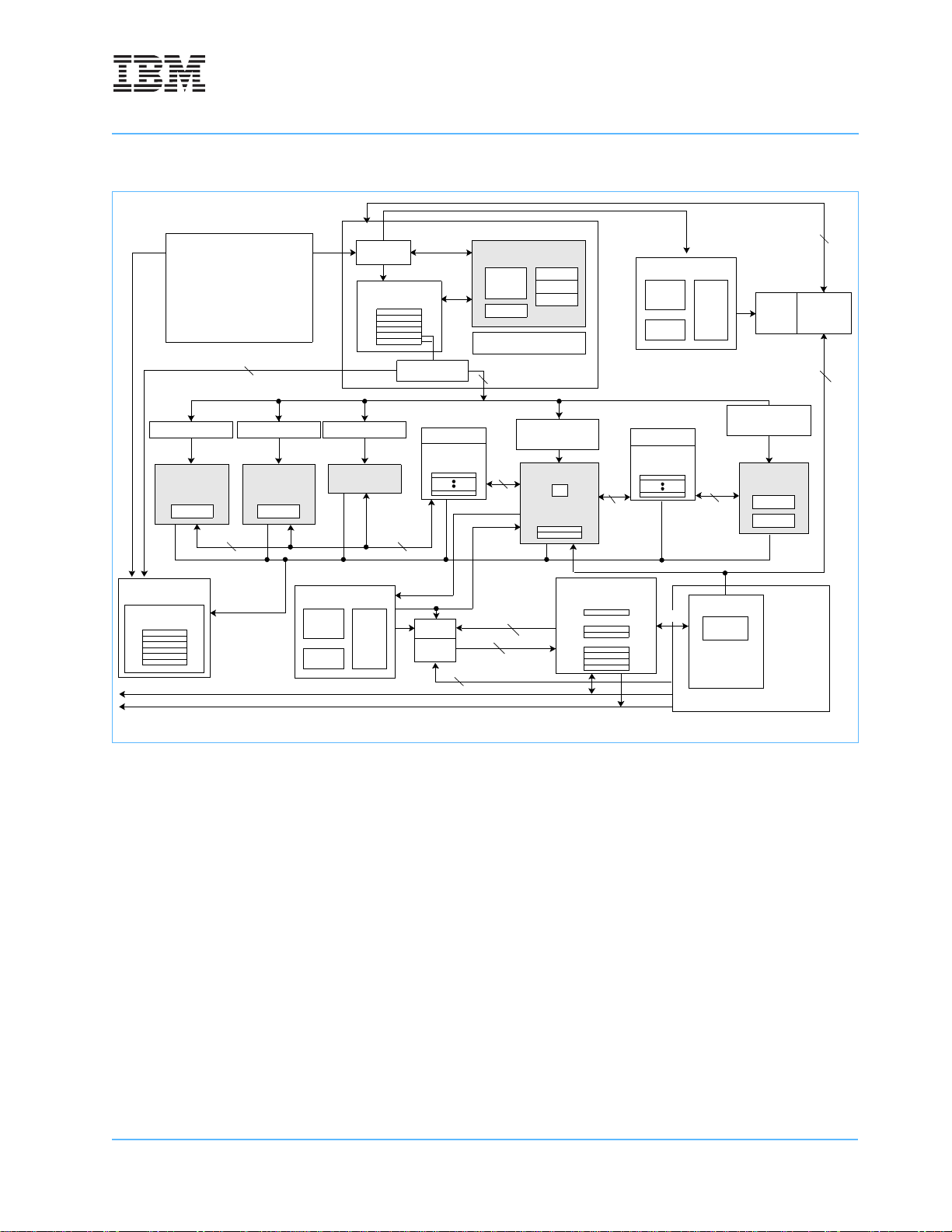
Figure 1-1. 750GX Microprocessor Block Diagram
User’s Manual
IBM PowerPC 750GX and 750GL RISC Microproces sor
Additional Features:
Reservation Stat io n
Integer Unit 1
+ x ÷
Completion Unit
Reorder Buffer
(6 Entry)
• Time Base Cntr/
Decrementer
• Clock Multiplier
• JTAG/COP Interface
• Thermal/Power
Management
• Performance Monitor
2 Instructions
Reservation Station Reservation Station
Integer Unit 2
+
32-Bit
60x Bus
System Reg ister
Data MMU
SRs
(Original)
DTLB
Ifetch
Instruction Queue
(6 Words)
Unit
32-Bit
DBAT
Array
Instruction Control Unit
Dispatch Unit
GPR File
Rename Buffers
(6)
PA
EA
Tags
32-KB
D Cache
256-Bit
Branch Processing
Unit
BTIC
64 Entries
BHT
Interrupt Logic
64-Bit
(2 Instructions)
Reservation Station
Load/Store Unit
32-Bit
(EA Calculation)
Store Queue
64-Bit
256-Bit
32-Bit Address Bus
64-Bit Data Bus
CTR
LR
CR
(2 Entry)
64-Bit
+
60x Bus Interface Unit
Instruction Fetch Queue
L1 Castout Queue
Data Load Queue
Instruction MMU
SRs
(Shadow)
ITLB
FPR File
Rename Buffers
(6)
64-Bit
IBAT
Array
Reservation Station
64-Bit
L2 Cache
L2CR
L2 Tag
1 MB
SRAM
(4 Instructions)
Tags
(2 Entry)
Floating-Point
Unit
+ x ÷
FPSCR
FPSCR
128-Bit
64-Bit
32-KB
I Cache
1.2 750GX Microprocessor Features
This section lists features of the 750GX. The interrelationship of these features is shown in Figure 1-1 on
page 25.
Major features of 750GX are:
• High-performance, su pers cal ar mic rop roc es sor.
– As many as four instructions can be fetched from the instruction cache per clock cycle.
– As many as two instructions can be dispatched and completed per clock.
– As many as six instructions can execute per clock (including two integer instructions).
– Single-clock-cycle executi on for most instructions.
• Six independent execution units and two register files.
– BPU featuring both static and dynamic branch prediction.
• 64-entry (16-set, 4-way set-associative) branch target instruction cache (BTIC), a cache of
branch instructions that have been encountered in branch/loop code sequences. If a target
instruction is in the BTIC, it is fetched into the instruction queue a cycle sooner than it can be
gx_01.fm.(1.2)
March 27,2006
PowerPC 750GX Overview
Page 25 of 377
Page 26

User’s Manual
IBM PowerPC 750GX and 750GL RISC Microprocessor
made available from the instruction cache. Typically, if a fetch access hits the BTIC, it provides
the first two instructions in the target stream effectively yielding a zero-cycle branch.
• 512-entry branch history table (BHT) with two bits per entry for four levels of prediction—nottaken, strongly not-taken, taken, strongly taken.
• Removal of Branch instructions that do not update the Count Register (CTR) or Link Register
(LR) from the instruction stream.
– Two integer units (IUs) that share 32 general purpose registers (GPRs) for integer operands.
• IU1 can execute any integer instruction.
• IU2 can execute all integer instructions except multiply and divide instructions (multiply, divide,
shift, rotate, arithmetic, and logical instructions). Most instructions that execute in the IU2 take
one cycle to execute. The IU2 has a single-entry reservation station.
– 3-stage floating-point unit (FPU).
• FPU fully compliant with IEEE
®
754-1985 for both single-precision and double-precision opera-
tions.
• Support for non-IEEE mode for time-critical operations.
• Hardware support for denormalized numbers.
• Hardware support for divide.
• 2-entry reservation station.
• Thirty-two 64-bit Floating Point Registers (FPRs) for single and double-precision operations.
– 2-stage load/store unit (LSU).
• 2-entry reservation station.
• 4-entry load queue.
• Single-cycle, pipelined cache access.
• Dedicated adder performs effective address (EA) calculations.
• Performs alignment and precision conversion for floating-point data.
• Performs alignment and sign extension for integer data.
• 3-entry store queue.
• Supports both big-endian and little-endian modes.
– System register unit (SRU) handles miscellaneous instructions.
• Executes Condition Register (CR) logical and Move-to/Move-from SPR instructions (mtspr and
mfspr).
• Single-entry reservation station.
• Rename buffers.
– Six GPR rename buffers.
– Six FPR rename buffers.
– Condition Register buffering supports two CR writes per clock.
• Completion unit.
– The completion unit retires an instruction from the 6-entry reorder buffer (completion queue) when all
instructions ahead of it have been completed, the instruction has finished execution, and no excep-
tions are pending.
– Guarantees a sequential programming model and a precise-exception model.
– Monitors all dispatched instructions and retires them in order.
– Tracks unresolved branches and flushes instructions from the mispredicted branch path.
PowerPC 750GX Overview
Page 26 of 377
gx_01.fm.(1.2)
March 27,2006
Page 27

User’s Manual
IBM PowerPC 750GX and 750GL RISC Microproces sor
– Retires as many as two instructions per clock.
• Separate on-chip L1 instruction and data caches (Harvard architecture).
– 32-KB, 8-way set-associative instruction and data caches.
– Pseudo least-recently-used (PLRU) replacement algorithm.
– 32-byte (8-word) cache block.
– Physically indexed/physical tags.
Note: The PowerPC Architecture refers to physical address space as real address space.
– Cache write-back or write-through operation programmable on a virtual-page or BAT-block basis.
– Instruction cache can provide four instructions per clock; data cache can provide two words per clock
– Caches can be disabled in software.
– Caches can be locked in software.
– Data-cache coherency (MEI) maintained in hardware.
– The critical double word is made available to the requesting unit when it is read into the line-fill buffer.
The cache is nonblocking, so it can be accessed during block reload.
– Nonblocking instruction cache (one outstanding miss).
– Nonblocking data cache (four outstanding misses).
– No snooping of instruction cache.
– Parity for L1 tags and cach es.
• Integrated L2 cache.
– 1-MB on-chip ECC SRAMs.
– On-chip 4-way set-associative tag memory.
– ECC error correction for most single-bit errors; detection of remaining single-bit errors and all double-
bit errors.
– Copy-back or write-through data cache on a page basis, or for entire L2.
– 64-byte line size, two sectors per line.
– L2 frequency at core speed.
– On-board ECC; parity for L2 tags.
– Supports up to four outstanding misses (three data and one instruction or four data).
– Cache locking by way.
• Separate memory management units (MMUs) for instructions and data.
– 52-bit virtual address; 32-b it phy si cal address.
– Address translation for virtual pages or variable-sized BAT blocks.
– Memory programmable as write-back or write-through, cacheable or noncacheable, and coherency
enforced or coherency not enforced on a virtual-page or BAT block basis.
– Separate IBAT and DBAT arrays (eight each) for instructions and data, respectively.
– Separate virtual instruction and data translation lookaside buffers (TLBs).
• Both TLBs are 128-entry, 2-way set associative, and use an LRU replacement algorithm.
gx_01.fm.(1.2)
March 27,2006
PowerPC 750GX Overview
Page 27 of 377
Page 28

User’s Manual
IBM PowerPC 750GX and 750GL RISC Microprocessor
• TLBs are hardware-reloadable (the page table search is performed by hardware).
• Bus interface features:
– Enhanced 60x bus that pipelines back-to-back reads to a depth of four. A dedicated snoop queue that
allows snoop copybacks to also pipeline with up to the four maximum reads. Enveloped write transactions supported with the asserti on of DBWO
.
– Selectable bus-to-core clock frequency ratios of 2x, 2.5x, 3x, 3.5x, 4x, 4.5x, 5x, 5.5x, 6x, 6.5x, 7x,
7.5x, 8x, 8.5x, 9x, 9.5x, 10x, 11x, 12x, 13x, 14x, 15x, 16x, 17x, 18x, 19x, and 20x supported (2x, 2.5x,
3x, and 3.5x not supported with bus pipelining enabled).
– A 64-bit, split-transaction external data bus with burst transfers.
– Support for address pipelining and limited out-of-order bus transactions.
– 8-word reload buffer for the L1 data cache.
– Single-entry instruction fetch queue.
– 2-entry L2 cache castout queue.
–No-DRTRY
mode eliminates the DRTRY signal from the qualified bus grant. This allows the forwarding of data during load operations to the internal core one bus cycle sooner than if the use of DRTRY
is enabled.
– Selectable I/O interface voltages of 1.8 V, 2.5 V, or 3.3 V
• Multiprocessing support features:
– Hardware-enforced, 3-state cache-coherency protocol (MEI) for data cache.
– Load/store with reservation instruction pair for atomic memory references, semaphores, and other
multiprocessor operations.
• Power and thermal management:
– Three static modes, doze, nap, and sleep, progressively reduce power dissipation:
• Doze—All the functional units are disabled except for the Time Base/Decrementer Registers and
the bus snooping logic.
• Nap—The nap mode further reduces power consumption by disabling bus snooping, leaving only
the Time Base Register and the PLL in a powered state.
• Sleep—All internal functional units are disabled, after which external system logic can disable the
PLL and SYSCLK.
– Software-controllable thermal management. Thermal management is performed through the use of
three supervisor-level registers and a 750GX-specific thermal-management exception.
– Software-controlled frequency switching (dual PLL mode) to allow toggling between minimum and
maximum frequencies to manage power consumption based on computational load.
– Instruction-cache throttling provides control to slow instruction fetching to limit power consumption.
• Hardware-assist features for fault-tolerant systems including L2 ECC correction, parity checking on internal arrays, and dual-processor lockstep operation.
• Performance monitor can be used to help debug system designs and improve software efficiency.
• In-system testability and debugging features through Joint Test Action Group (JTAG) boundary-scan
capability.
PowerPC 750GX Overview
Page 28 of 377
gx_01.fm.(1.2)
March 27,2006
Page 29

User’s Manual
IBM PowerPC 750GX and 750GL RISC Microproces sor
1.2.1 Instruction Flow
As shown in Figure 1-1, 750GX Microprocessor Block Diagram, on page 25, the 750GX instruction control
unit provides centralized control of instruction flow to the execution units. The instruction unit contains a
sequential instruction fetch (Ifetch), 6-entry instruction queue (IQ), dispatch unit, and BPU. It determines the
address of the next instruction to be fetched based on information from the sequential instruction fetcher and
from the BPU. See Chapt er 6, I nst ru cti on Timing, on page 209 for more information.
The sequential instruction fetcher loads instructions from the instruction cache into the instruction queue. The
BPU extracts branch instructions from the sequential instruction fetcher. Branch instructions that cannot be
resolved immediately are predicted using either 750GX-specific dynamic branch prediction or the architecture-defined static branch prediction.
Branch instructions that do not update the LR or CTR are removed from (folded out of) the instruction stream.
Instruction fetching continues along the predicted path of the branch instruction.
Instructions issued to execution units beyond a predicted branch can be executed but are not retired until the
branch is resolved. If branch prediction is incorrect, the completion unit flushes all instructions fetched on the
predicted path, and instruction fetching resumes along the correct path.
1.2.1.1 Instruction Queue and Dispatch Unit
The instruction queue (IQ), shown in Figure 1-1 on page 25, holds as many as six instructions and loads up to
four instructions from the instruction cache during a single-processor clock cycle. The instruction fetcher
continuously attempts to load as many instructions as there were vacancies created in the IQ in the previous
clock cycle. All instructions except branches are dispatched to their respective execution units from the
bottom two positions in the instruction queue (IQ0 and IQ1) at a maximum rate of two instructions per cycle.
Reservation stations are provided for the IU1, IU2, FPU, LSU, and SRU for dispatched instructions. The
dispatch unit checks for source and destination register dependencies, allocates rename buffers, determines
whether a position is available in the completion queue, and inhibits subsequent instruction dispatching if
these resources are not available.
Branch instructions can be detected, decoded, and predicted from anywhere in the instruction queue. For a
more detailed discussion of instruction dispatch, see Section 6.6.1, Branch, Dispatch, and Completion-Unit
Resource Requirements, on page 237.
1.2.1.2 Branch Processing Unit (BPU)
The BPU receives branch instructions from the sequential instruction fetcher and performs CR lookahead
operations on conditional branches to resolve them early, achieving the effect of a zero-cycle branch in many
cases.
Unconditional branch instructions and conditional branch instructions in which the condition is known can be
resolved immediately. For unresolved conditional branch instructions, the branch path is predicted using
either the architecture-defined static branch prediction or 750GX-specific dynamic branch prediction.
Dynamic branch prediction is enabled if the BHT bit in Hardware-Implementation-Dependent Register 0 is set
(HID0[BHT] = 1).
When a prediction is made, instruction fetching, dispatching, and execution continue along the predicted
path, but instructions cannot be retired and write results back to architected registers until the prediction is
determined to be correct (resolved). When a prediction is incorrect, the instructions from the incorrect path
gx_01.fm.(1.2)
March 27,2006
PowerPC 750GX Overview
Page 29 of 377
Page 30

User’s Manual
IBM PowerPC 750GX and 750GL RISC Microprocessor
are flushed from the processor, and instruction fetching resumes along the correct path. The 750GX allows a
second branch instruction to be predicted; instructions from the second predicted branch instruction stream
can be fetched but cannot be dispatched. These instructions are held in the instruction queue.
Dynamic prediction is implemented using a 512-entry BHT. The BHT is a cache that provides two bits per
entry that together indicate four levels of prediction for a branch instruction—not-taken, strongly not-taken,
taken, strongly taken. When dynamic branch prediction is disabled, the BPU uses a bit in the instruction
encoding to predict the direction of the conditional branch. Therefore, when an unresolved conditional branch
instruction is encountered, the 750GX executes instructions from the predicted path although the results are
not committed to architected registers until the conditional branch is resolved. This execution can continue
until a second unresolved branch instruction is encountered.
When a branch is taken (or predicted as taken), the instructions from the untaken path must be flushed, and
the target instruction stream must be fetched into the IQ. The BTIC is a 64-entry cache that contains the most
recently used branch target instructions, typically in pairs. When an instruction fetch hits in the BTIC, the
instructions arrive in the instruction queue in the next clock cycle, a clock cycle sooner than they would arrive
from the instruction cache. Additional instructions arrive from the instruction cache in the next clock cycle.
The BTIC reduces the number of missed opportunities to dispatch instructions and gives the processor a
1-cycle head start on processing the target stream. With the use of the BTIC, the 750GX achieves a zerocycle delay for branches taken. Coherency of the BTIC table is maintained by table reset on an instructioncache flash invalidate, Instruction Cache Block Invalidate (icbi) or Return from Interrupt (rfi) instruction
execution, or when an exception is taken.
The BPU contains an adder to compute branch target addresses and three user-control registers—the Link
Register (LR), the Count Register (CTR), and the CR. The BPU calculates the return pointer for subroutine
calls and saves it into the LR for certain types of branch instructions. The LR also contains the branch target
address for the Branch Conditional to Link Register (bclrx) instruction. The CTR contains the branch target
address for the Branch Conditional to Count Register (bcctrx) instruction. Because the LR and CTR are
special purpose registers (SPRs), their contents can be copied to or from any GPR. Since the BPU uses dedicated registers rather than GPRs or FPRs, execution of branch instructions is largely independent from
execution of fixed-point and floating-point instructions.
1.2.1.3 Completion Unit
The completion unit operates closely with the dispatch unit. Instructions are fetched and dispatched in
program order. At the point of dispatch, the program order is maintained by assigning each dispatched
instruction a successive entry in the 6-entry completion queue. The completion unit tracks instructions from
dispatch through execution and retires them in program order from the two bottom entries in the completion
queue (CQ0 and CQ1).
Instructions cannot be dispatched to an execution unit unless there is a vacancy in the completion queue and
rename buffers are available. Branch instructions that do not update the CTR or LR are removed from the
instruction stream and do not occupy a space in the completion queue. Instructions that update the CTR and
LR follow the same dispatch and completion procedures as nonbranch instructions, except that they are not
issued to an execution unit.
An instruction is retired when it is removed from the completion queue and its results are written to architected registers (GPRs, FPRs, LR, and CTR) from the rename buffers. In-order completion ensures program
integrity and the correct architectural state when the 750GX must recover from a mispredicted branch or any
exception. Also, the rename buffers assigned to it by the dispatch unit are returned to the available rename
buffer pool. These rename buffers are reused by the dispatch unit as subsequent instructions are dispatched.
PowerPC 750GX Overview
Page 30 of 377
gx_01.fm.(1.2)
March 27,2006
Page 31

User’s Manual
IBM PowerPC 750GX and 750GL RISC Microproces sor
For a more detailed discussion of instruction completion, see Section 6.6.1, Branch, Dispatch, and Completion-Unit Resource Requirements, on page 237.
1.2.2 Independent Execution Units
In addition to the BPU, the 750GX has the following five execution units:
• Two integer units (IUs)
• Floating-point unit (FPU)
• Load/store unit (LSU)
• System register unit (SRU)
1.2.2.1 Integer Units (IUs)
The integer units, IU1 and IU2, are shown in Figure 1-1 on page 25. IU1 can execute any integer instruction;
IU2 can execute any integer instruction except multiplication and division instructions. Each IU has a singleentry reservation station that can receive instructions from the dispatch unit and operands from the GPRs or
the rename buffers. The output of the IU is latched in the rename buffer assigned to the instruction by the
dispatch unit.
Each IU consists of three single-cycle subunits—a fast adder/comparator, a subunit for logical operations,
and a subunit for performing rotates, shifts, and count-leading-zero operations. These subunits handle all
1-cycle arithmetic and logica l integer instructions; only one subunit can execute an instruction at a time.
The IU1 has a 32-bit integer multiplier/divider, as well as the adder, shift, and logical units of the IU2. The
multiplier supports early exit for operations that do not require full 32 × 32-bit multiplication. Multiply and
divide instructions spend several cycles in the execution stage before the results are written to the output
rename buffer.
1.2.2.2 Floating-Point Unit (FPU)
The FPU, shown in Figure 1-1 on page 25, is designed as a 3-stage pipelined processing unit, where the first
stage is for multiply, the second stage is for add, and the third stage is for normalize. A single-precision
multiply/add operation is processed with 1-cycle throughput and 3-cycle latency. (A single-precision instruction spends one cycle in each stage of the FPU). A double-precision multiply requires two cycles in the
multiply stage and one cycle in each additional stage. A double-precision multiply/add has a 2-cycle
throughput and a 4-cycle latency. As instructions are dispatched to the FPU reservation station, source
operand data can be accessed from the FPRs or from the FPR rename buffers. Results, in turn, are written to
the rename buffers and are made available to subsequent instructions. Instructions pass through the reservation station and the pipeline stages in program order. Stalls due to contention for FPRs are minimized by
automatic allocation of the six floating-point rename buffers. The completion unit writes the contents of the
rename buffer to the appropriate FPR when floating-point instructions are retired.
The 750GX supports all IEEE 754-1985 floating-point data types (normalized, denormalized, not a number
(NaN), zero, and infinity) in hardware, eliminating the latency incurred by software exception routines. (Note
that “exception” is also referred to as “interrupt” in the architecture specification.)
gx_01.fm.(1.2)
March 27,2006
PowerPC 750GX Overview
Page 31 of 377
Page 32

User’s Manual
IBM PowerPC 750GX and 750GL RISC Microprocessor
1.2.2.3 Load/Store Unit (LSU)
The LSU executes all load-and-store instructions and provides the data-transfer interface between the GPRs,
FPRs, and the data-cache/memory subsystem. The LSU functions as a 2-stage pipelined unit, which calculates effective addresses in the first stage. In the second stage, the address is translated, the cache is
accessed, and the data is aligned if necessary. Unless extensive data alignment is required (for example, to
cross a double-word boundary), the instructions complete in two cycles with a 1-cycle throughput. The LSU
also provides sequencing for load/store string and multiple register transfer instructions.
Load-and-store instructions are translated and issued in program order. However, some memory accesses
can occur out of order. Synchronizing instructions can be used to enforce strict ordering if necessary. When
there are no data dependencies and the guard bit for the page or block is cleared, a maximum of one out-oforder cacheable load operation can execute per cycle, with a 2-cycle total latency on a cache hit. Data
returned from the cache is held in a rename buffer until the completion logic commits the value to a GPR or
FPR. Stores cannot be executed out of order and are held in the store queue until the completion logic
signals that the store operation is to be completed to memory. The 750GX executes store instructions with a
maximum throughput of one per cycle and a 3-cycle latency to the data cache. The time required to perform
the actual load or store operation depends on the processor/bus clock ratio and whether the operation
involves the L1 cache, the L2 cache, system memory, or an I/O device.
The L/S unit has two reservation stations, Eib0 and Eib1. For loads, there is also a hold queue and a miss
queue. A load that misses in the dcache advances from Eib0 to the miss queue, where only necessary state
for instruction completion like the instruction ID and register rename ID are stored. If another load misses
under an outstanding miss, then it is held in the hold queue and Eib0 is free. Two more load instructions may
now be dispatched to Eib0 and Eib1. The Miss-under-Miss feature allows the hold, Eib0, and Eib1 load
requests to proceed out to the bus, even though there is an outstanding miss that would normally stall the
pending loads.
1.2.2.4 System Register Unit (SRU)
The SRU executes various system-level instructions, as well as Condition Register logical operations and
Move-to/Move-from Special-Purpose Register instructions. To maintain system state, most instructions
executed by the SRU are execution-serialized with other instructions; that is, the instruction is held for execution in the SRU until all previously issued instructions have been retired. Results from execution-serialized
instructions executed by the SRU are not available or forwarded for subsequent instructions until the instruction completes.
1.2.3 Memory Management Units (MMUs)
The 750GX’s MMUs support up to 4 petabytes (252) of virtual memory and 4 gigabytes (232) of physical
memory for instructions and data. The MMUs also control access privileges for these spaces on block and
page granularities. Referenced and changed status is maintained by the processor for each page to support
demand-paged virtual memory systems.
The LSU, with the aid of the MMU, translates effective addresses for data loads and stores. The effective
address is calculated on the first cycle, and the MMU translates it to a physical address at the same time it is
accessing the L1 cache on the second cycle. The MMU also provides the necessary control and protection
information to complete the access. By the end of the second cycle, the data and control information is available if no miss conditions for translate and cache access were encountered. This yields a 1-cycle throughput
and a 2-cycle latency.
PowerPC 750GX Overview
Page 32 of 377
gx_01.fm.(1.2)
March 27,2006
Page 33

User’s Manual
IBM PowerPC 750GX and 750GL RISC Microproces sor
The 750GX supports the following types of memory translation:
Real-addressing mode In this mode, translation is disabled (control bit MSR(IR) = 0 for instructions and
control bit MSR(DR) = 0 for data). The effective address is used as the physical
address to access memory.
Virtual-page-address
translation
Translates from an effective address to a physical address by using the Segment
Registers and the TLB and access data from a 4-KB virtual page. This page is
either in physical memory or on disk. If the latter, a page-fault exception occurs.
Block-address
translation
Translates the effective address into a physical address by using the BAT Registers and accesses a block (128 KB to 256 MB) in memory.
If translation is enabled, the appropriate MMU translates the higher-order bits of the effective address into
physical address bits by using either BATs or the page translation method. The lower-order address bits,
which are untranslated and therefore, considered both logical and physical, are directed to the L1 caches
where they form the index into the 8-way set-associative tag and data arrays. After translating the address,
the MMU passes the higher-order physical address bits to the cache, and the cache lookup completes. For
caching-inhibited accesses or accesses that miss in the cache, the untranslated lower-order address bits are
concatenated with the translated higher-order address bits. The resulting 32-bit physical address is used and
accesses the L2 cache or system memory via the 60x bus.
If the BAT Registers are enabled and the address translates via this method, the page translation is canceled
and the high-order physical address bits from the BAT Register are forward to the cache/memory access
system. There are eight 8-byte BAT Registers, which function like an associative memory. These registers
provide cache-control and protection information as well as address translation. Only one of the eight BAT
entries should translate a given effective address.
If address relocation is enabled and the effective address does not translate via the BAT method, the virtualpage method is used. The four high-order bits of the effective address are used to access the 16-entry
Segment Register array. From this array, a 24-bit Segment Register is accessed and used to form the highorder bits of a 52-bit virtual address. The low-order 28 bits of the effective address are used to form the loworder bits of the virtual address. This 52-bit virtual address is translated into a physical address by doing a
lookup in the TLB. If the lookup is successful, a physical address is formed by using 16 low-order bits from the
virtual address and 16 high-order bits from the TLB. The TLB also provides cache-control and protection
information to be used by the cache/memory system.
TLBs are 128-entry, 2-way, set-associative caches that contain information about recently translated virtual
addresses. When an address translation is not in a TLB, the 750GX automatically generates a page table
search in memory to update the TLB. This search could find the desired entry in the L1 or L2 cache or in the
page table in memory. The time to reload a TLB entry depends on where it is found; it could be completed in
just a few cycles. If memory is searched, a maximum of 16 bus cycles would be needed before a page-fault
exception is signaled.
1.2.4 On-Chip Level 1 Instruction and Data Caches
The 750GX implements separate instruction and data caches. Each cache is 32-KB and 8-way set-associative. The caches are physically indexed. Each cache block contains eight contiguous words from memory that
are loaded from an 8-word boundary (bits EA[27–31] are zeros); thus, a cache block never crosses a page
boundary. A miss in the L1 cache causes a block reload from either the L2 cache, if the block is in the L2
cache, or from main memory. The critical double word is accessed first, forwarded to the load/store unit, and
gx_01.fm.(1.2)
March 27,2006
PowerPC 750GX Overview
Page 33 of 377
Page 34

User’s Manual
IBM PowerPC 750GX and 750GL RISC Microprocessor
written into an 8-word buffer. Subsequent double words are fetched from either the L2 cache or the system
memory and written into the buffer. Once the total block is in the buffer, the line is written into the L1 cache in
a single cycle. This minimizes write cycles into the L1 cache, leaving more read/write cycles available to the
LSU. The L1 is nonblocking and supports hits under misses during this block reload sequence. Misaligned
accesses across a block or page boundary can incur a performance penalty. The 750GX L1 data cache
supports miss-under-miss access, meaning that with one miss outstanding, the cache can continue to be
accessed for up to three more misses. The 750GX L1 data cache also allows the additional misses to initiate
a transaction in the bus interface unit, while the first miss is pending.
The 750GX L1 cache organization is shown in Figure 1-2, L1 Cache Organization.
Figure 1-2. L1 Cache Organiz ati on
128 Sets
Way 0
Way 1
Way 2
Way 3
Way 4
Way 5
Way 6
Way 7
Address Tag 0
Address Tag 1
Address Tag 2
Address Tag 3
Address Tag 4
Address Tag 5
Address Tag 6
Address Tag 7
State
State
State
State
State
State
State
State
Words [0–7]
Words [0–7]
Words [0–7]
Words [0–7]
Words [0–7]
Words [0–7]
Words [0–7]
Words [0–7]
8 Words/Way
The data cache provides double-word accesses to the LSU each cycle. Like the instruction cache, the data
cache can be invalidated all at once or on a per-cache-block basis. The data cache can be disabled and
invalidated by clearing the data-cache enable bit (HID0[DCE]) and setting the data-cache flash invalidate bit
(HID0[DCFI]). The data cache can be locked by setting HID0[DLOCK]. To ensure cache coherency, the data
cache supports the 3-state MEI protocol. The data-cache tags are single-ported, so a simultaneous load or
store and a snoop access represent a resource collision, and an LSU access is delayed for one cycle. If a
snoop hit occurs and a castout is required, the LSU is blocked internally for one cycle to allow the 8-word
block of data to be copied to the write-back buffer.
The instruction cache provides up to four instructions to the instruction queue in a single cycle. Like the data
cache, the instruction cache can be invalidated all at once or on a cache-block basis. The instruction cache
can be disabled and invalidated by clearing the instruction-cache enable bit (HID0[ICE]) and setting the
PowerPC 750GX Overview
Page 34 of 377
gx_01.fm.(1.2)
March 27,2006
Page 35

User’s Manual
IBM PowerPC 750GX and 750GL RISC Microproces sor
instruction-cache flash invalidate bit (HID0[ICFI]). The instruction cache can be locked by setting
HID0[ILOCK]. The instruction cache supports only the valid and invalid states, and requires software to maintain coherency if the underlying program changes.
The 750GX also implements a 64-entry (16-set, 4-way set-associative) branch target instruction cache
(BTIC). The BTIC is a cache of branch instructions that have been encountered in branch/loop code
sequences. If the target instruction is in the BTIC, it is fetched into the instruction queue a cycle sooner than it
can be made available from the instruction cache. Typically, the BTIC contains the first two instructions in the
target stream. The BTIC can be disabled and invalidated through software.
Coherency of the BTIC is transparent to the running software and is coupled with various functions in the
750GX processor. When the BTIC is enabled and loaded with instruction pairs to support zero-cycle delay on
branches taken, the table must be invalidated if the underlying program changes. (This is also true for the
instruction cache.) The BTIC is invalidated on an instruction-cache flash invalidate, an icbi or rfi instruction,
and any exception.
For more information and timing examples showing cache hit and cache miss latencies, see Section 6.3.2,
Instruction Fetch Timing, on page 216.
1.2.5 On-Chip Level 2 Cache Implementation
The L2 cache is a unified cache that receives memory requests from both the L1 instruction and data caches
independently. The L2 cache is implemented with an L2 Cache Control Register (L2CR), an on-chip, 4-way,
set-associative tag array, and with a 1-MB, integrated SRAM for data storage. The L2 cache normally operates in write-back mode and supports cache coherency through snooping. The access interface to the L2 is
64 bits for writes and requires four cycles to write a single cache block. The access interface to the L2 is 256
bits for reads and requires one cycle to read a single cache block. The L2 uses ECC on a double word,
corrects most single-bit errors, and detects the remaining single-bit errors and all double-bit errors. See
Figure 9-1, L2 Cache, on page 327.
The L2 cache is organized with 64-byte lines, which in turn are subdivided into 32-byte blocks, the unit at
which cache coherency is maintained. This reduces the size of the tag array, and one tag supports two cache
blocks. Each 32-byte cache block has its own valid and modified status bits. When a cache line is removed,
the contents of both blocks and the tag are removed from the L2 cache. The cache block is only written to
system memory if the modified bit is set.
Requests from the L1 cache generally result from instruction misses, data load or store misses, write-through
operations, or cache-management instructions. Misses from the L1 cache are looked up in the L2 tags and
serviced by the L2 cache if they hit; they are forwarded to the 60x bus interface if they miss.
The L2 cache can accept multiple, simultaneous accesses. However, they are serialized and processed one
per cycle. The L1 instruction cache can request an instruction at the same time that the L1 data cache
requests one load and two store operations. The L2 cache also services snoop requests from the bus. If there
are multiple pending requests to the L2 cache, snoop requests have highest priority. Load-and-store requests
from the L1 data cache have the next highest priority. The last priority consists of instruction fetch requests
from the L1 instruction cache.
1.2.6 System Interface/Bus Interface Unit (BIU)
The PowerPC 750GX uses a reduced system signal set, which eliminates some optional 60x bus protocol
pins. The system designer needs to make note of these differences.
gx_01.fm.(1.2)
March 27,2006
PowerPC 750GX Overview
Page 35 of 377
Page 36

User’s Manual
IBM PowerPC 750GX and 750GL RISC Microprocessor
The address and data buses operate independently. Address and data tenures of a memory access are
decoupled to provide more flexible control of bus traffic. The primary activity of the system interface is transferring data and instructions between the processor and system memory. There are two types of memory
accesses:
Single-beat transfers Allow transfer sizes of 8, 16, 24, 32, or 64 bits in one bus clock cycle. Single-beat
transactions are caused by uncacheable read and write operations that access
memory directly when caches are disabled, for cache-inhibited accesses, and for
stores in write-through mode. The two latter accesses are defined by control bits
provided by the MMU during address translation.
4-beat burst (32-byte)
data transfers
Burst transactions, which always transfer an entire cache block (32 bytes), are initiated when an entire cache block is transferred. If the caches on the 750GX are
enabled and using write-back mode, burst-read operations are the most common
memory accesses, followed by burst-write memory operations.
The 750GX also supports address-only operations, which are variants of the burst and single-beat operations
(for example, atomic memory operations and global memory operations that are snooped), and address retry
activity (for example, when a snooped read access hits a modified block in the cache). The broadcast of
some address-only operations is controlled through the address broadcast enable bit (HID0[ABE]). I/O
accesses use the same protocol as memory accesses.
Access to the system interface is granted through an external arbitration mechanism that allows devices to
compete for bus mastership. This arbitration mechanism is flexible, allowing the 750GX to be integrated into
systems that implement various fairness and bus-parking procedures to avoid arbitration overhead.
Typically, memory accesses are weakly ordered—sequences of operations, including load/store string and
multiple instructions, do not necessarily complete in the order they begin. This maximizes the efficiency of the
bus without sacrificing data coherency. The 750GX allows read operations to go ahead of store operations
except when a dependency exists, or when a noncacheable access is performed. It also allows a write operation to go ahead of a previously queued read data tenure (for example, letting a snoop push be enveloped
between address and data tenures of a read operation). Because the 750GX can dynamically optimize runtime ordering of load/store traffic, overall performance is improved.
The system interface is specific for each PowerPC microprocessor implementation.
The 750GX signals are grouped as shown in Figure 1-3, System Interface. Test and control signals provide
diagnostics for selected internal circuits.
PowerPC 750GX Overview
Page 36 of 377
gx_01.fm.(1.2)
March 27,2006
Page 37

Figure 1-3. System Interface
User’s Manual
IBM PowerPC 750GX and 750GL RISC Microproces sor
Address Arbitration
Address Start
Address Transfer
750GX
Transfer Attribute
Address Termination
Interrupt
VDD VDD (I/O)
Data Arbitration
Data Transfer
Data Termination
Test and Control
Clocks
Processor Status/Control
The system interface supports address pipelining, which allows the address tenure of one transaction to
overlap the data tenure of another. The 750GX can support up to five outstanding transactions on the bus,
including up to one snoop copyback, up to four loads, and up to four stores. The extent of the pipelining
depends on external arbitration and control circuitry. Similarly, the 750GX supports split-bus transactions for
systems with multiple potential bus masters—one device can be master of the address bus while another is
master of the data bus. Allowing multiple bus transactions to occur simultaneously increases the available
bus bandwidth for other activity.
The 750GX’s clocking structure supports a wide range of processor-to-bus clock ratios.
1.2.7 Signals
The 750GX’s signals are grouped as follows:
Address arbitration The 750GX uses these signals to arbitrate for address-bus mastership.
Address start This signal indicates that a bus master has begun a transaction on the address
bus.
Address transfer These signals include the address bus and are used to transfer the address.
Transfer attribute These signals provide information about the type of transfer, such as the transfer
size and whether the transaction is burst, write-through, or caching-inhibited.
Address termination These signals are used to acknowledge the end of the address phase of the trans-
action. They also indicate whether a condition exists that requires the address
phase to be repeated.
Data arbitration The 750GX uses these signals to arbitrate for data-bus mastership.
Data transfer These signals include the data bus and are used to transfer the data.
Data termination These signals are required after each data beat in a data transfer. In a single-beat
transaction, a data termination signal also indicates the end of the tenure. In burst
accesses, data termination signals apply to individual beats and indicate the end of
the tenure only after the final data beat.
gx_01.fm.(1.2)
March 27,2006
PowerPC 750GX Overview
Page 37 of 377
Page 38

User’s Manual
IBM PowerPC 750GX and 750GL RISC Microprocessor
Interrupt These signals include the interrupt signal, checkstop signals, and both soft reset
and hard reset signals. These signals are used to generate interrupt exceptions
and, under various conditions, to reset the processor.
Processor status/control These signals are used to indicate miscellaneous bus functions.
Clocks These signals determine the system clock frequency. These signals can also be
used to sync hronize multiprocessor systems.
Test and control The common on-chip processor (COP) unit provides a serial interface to the
system for performing board-level boundary scan interconnect tests.
Note: A bar over a signal name indicates that the signal is active low—for example, ARTRY (address retry)
and TS
(transfer start). Active-low signals are referred to as asserted (active) when they are low and as
negated when they are high. Signals that are not active low, such as A[0–31] (address-bus signals) and
TT[0–4] (transfer type signals) are referred to as asserted when they are high and as negated when they are
low.
1.2.8 Signal Configuration
Figure 1-4 shows the 750GX’s logical pin configuration. The signals are grouped by function.
PowerPC 750GX Overview
Page 38 of 377
gx_01.fm.(1.2)
March 27,2006
Page 39

Figure 1-4. 750GX Microprocessor Signal Groups
User’s Manual
IBM PowerPC 750GX and 750GL RISC Microproces sor
ADDRESS
ARBITRATION
ADDRESS START/
ADDRESS TRANSFER/
TRANSFER ATTRIBUTE
ADDRESS
TERMINATION
DATA
ARBITRATION
DATA
TRANSFER
DATA
TERMINATION
BR
BG
ABB
TS
A[0:31]
AP[0:3]
TT[0:4]
TBST
TSIZ[0:2]
GBL
WT
CI
AACK
ARTY
DBG
DBWO
DBB
D[0:63]
DP[0:7]
DBDIS
TA
DRTRY
TEA
1
1
1
1
32
4
5
1
3
1
1
1
750GX
1
1
1
1
1
64
8
1
1
1
1
1
1
1
1
1
1
1
1
1
1
1
1
1
5
1
2
INT
SMI
MCP
SRESET
HRESET
RSRVR
TBEN
TLBI SYNC
QREQ
QACK
CKSTP_IN
CKSTP_OUT
SYSCLK
PLL_CFG[0:4]
CLK_OUT
PLL_RNG[0:1]
INTERRUPTS/
RESETS
PROCESSOR
STATUS/
CONTROL
CLOCK
CONTROL
JTAG / COP
5
3
FACTORY TEST
TEST
INTERFACE
Signal functionality is described in detail in Chapter 7, Signal Descriptions, on page 249 and Chapter 8, Bus
Interface Operation, on page 279.
Note: See the PowerPC 750GX Datasheet for a complete list of signal pins.
gx_01.fm.(1.2)
March 27,2006
PowerPC 750GX Overview
Page 39 of 377
Page 40

User’s Manual
IBM PowerPC 750GX and 750GL RISC Microprocessor
1.2.9 Clocking
The 750GX requires a single system clock input, SYSCLK, that represents the bus interface frequency. Internally, the processor uses a phase-locked loop (PLL) circuit to generate a master core clock that is frequencymultiplied and phase-locked to the SYSCLK input. This core frequency is used to operate the internal
circuitry.
The PLL is configured by the PLL_CFG[0:4] signals, which select the multiplier that the PLL uses to multiply
the SYSCLK frequency up to the internal core frequency. In addition, the 750GX has two PLL_RNG bits that
set the proper operation frequency range. The feedback in the PLL guarantees that the processor clock is
phase locked to the bus clock, regardless of process variations, temperature changes, or parasitic capacitances.
The PLL also ensures a 50% duty cycle for the processor clock.
The 750GX supports various processor-to-bus clock frequency ratios, although not all ratios are available for
all frequencies. Configuration of the processor/bus clock ratios is displayed through a 750GX-specific
register, HID1. For information about supported clock frequencies, see the PowerPC 750GX Datasheet.
1.3 750GX Microprocessor Implementation
The PowerPC Architecture is derived from the Performance Optimized with Enhanced RISC (POWER™)
architecture. The PowerPC Architecture shares the benefits of the POWER architecture optimized for singlechip implementations. The PowerPC Architecture design facilitates parallel instruction execution, and is scalable to take advantage of future technological gains.
The remainder of this chapter describes the PowerPC Architecture in general, and specific details about the
implementation of 750GX as a low-power, 32-bit member of the PowerPC processor family. The structure of
the remainder of this chapter reflects the organization of the user’s manual; each section provides an overview of the corresponding chapter. The following sections summarize the features of the 750GX, distinguishing those that are defined by the architecture from those that are unique to the 750GX implementation.
Registers and
programming model
Section 1.4, PowerPC Registers and Programming Model, on page 42 describes
the registers for the operating environment architecture common among PowerPC
processors and describes the programming model. It also describes the registers
that are unique to the 750GX. The information in this section is described more fully
in Chapter 2, Programming Model, on page 57.
Instruction set and
addressing modes
Section 1.5, Instruction Set, on page 45 describes the PowerPC instruction set and
addressing modes for the PowerPC operating environment architecture, defines
the PowerPC instructions implemented in the 750GX, and describes new instruction set extensions to improve the performance of single-precision floating-point
operations and the capability of data transfer. The information in this section is
described more fully in Section 2.3, Instruction Set Summary, on page 86.
Cache implementation Section 1.6, On-Chip Cache Implementation, on page 47 describes the cache
model that is defined generally for PowerPC processors by the virtual environment
architecture. It also provides specific details about the 750GX L2 cache implementation. The information in this section is described more fully in Chapter 3, Instruc-
tion-Cache and Data-Cache Operation, on page 121.
PowerPC 750GX Overview
Page 40 of 377
gx_01.fm.(1.2)
March 27,2006
Page 41

User’s Manual
IBM PowerPC 750GX and 750GL RISC Microproces sor
Exception mode Section 1.7, Exception Model, on page 48 describes the exception model of the
PowerPC operating environment architecture and the differences in the 750GX
exception model. The information in this section is described more fully in
Chapter 4, Exceptions, on page 151.
Memory management Section 1.8, Memory Management, on page 51 describes in general terms the
conventions for memory management among the PowerPC processors. This
section also describes the 750GX’s implementation of the 32-bit PowerPC
memory-management specification. The information in this section is described
more fully in Chapter 5, Memory Management, on page 179.
Instruction timing Section 1.9, Instruction Timing, on page 52 provides a general description of the
instruction timing provided by the superscalar, parallel execution supported by the
PowerPC Architecture and the 750GX. The information in this section is described
in more detail in Chapter 6, Instruction Timing, on page 209.
Power management Section 1.10, Power Management, on page 54 describes how power management
can be used to reduce power consumption when the processor, or portions of it,
are idle. The information in this section is described more fully in Chapter 10,
Power and Thermal Management, on page 335.
Thermal management Section 1.11, Thermal Management, on page 55 desc rib es how the thermal-
management unit and its associated registers (THRM1–THRM4) and exception
processing can be used to manage system activity in a way that prevents
exceeding system and junction temperature thresholds. This is particularly useful in
high-performance portable systems, which cannot use the same cooling mechanisms (such as fans) that control overheating in desktop systems. The information
in this section is described more fu lly in Chapter 10, Power and Thermal Manage-
ment, on page 335.
Performance monitor Section 1.12, Performance Monitor, on page 56 describes the performance-
monitor facility, which system designers can use to help bring up, debug, and optimize software performance. The information in this section is described more fully
in Chapter 11, Performance Monitor and System Related Features, on page 349.
The PowerPC Architecture consists of the following layers, and adherence to the PowerPC Architecture can
be described in terms of which of the following levels of the architecture is implemented.
PowerPC user instruction
set architecture (UISA)
Defines the base user-level instruction set, user-level r egisters, data types,
floating-point exception model, memory models for a uniprocessor environment,
and programming model for a uniprocessor environment.
PowerPC virtual environment architecture (VEA)
Describes the memory model for a multiprocessor environment, defines cachecontrol instructions, and describes other aspects of virtual environments. Implementations that conform to the VEA also adhere to the UISA, but might not necessarily adhere to the OEA.
PowerPC operating
environment architecture
(OEA)
gx_01.fm.(1.2)
March 27,2006
Defines the memory-management model, supervisor-level registers, synchronization requirements, and the excep tio n m ode l. Impl eme ntat ion s that co nfor m to the
OEA also adhere to the UISA and the VEA.
PowerPC 750GX Overview
Page 41 of 377
Page 42

User’s Manual
IBM PowerPC 750GX and 750GL RISC Microprocessor
1.4 PowerPC Registers and Programming Model
The PowerPC Architecture defines register-to-register operations for most computational instructions. Source
operands for these instructions are accessed from the registers or are provided as immediate values
embedded in the instruction itself. The 3-register instruction format allows specification of a target register
distinct from the two source operands. Only load-and-store instructions transfer data between registers and
memory.
PowerPC processors have two levels of privilege: supervisor mode and user mode.The supervisor mode of
operation is typically used by the operating system. The user mode of operation, also called the problem
state, is typically used by the application software. The programming models incorporate 32 GPRs, 32 FPRs,
Special-Purpose Regis ters (SP Rs) , and se ve ra l misce ll ane ous regist er s. Ea ch PowerPC microprocessor
also has its own unique set of Hardware-Implementation-Dependent (HID) Registers.
While running in supervisor mode, the operating system is able to execute all instructions and access all
registers defined in the PowerPC Architecture. In this mode, the operating system establishes all address
translations and protection mechanisms, loads all Processor State Registers, and sets up all other control
mechanisms defined in the PowerPC 750GX processor. While running in user mode (problem state), many of
these registers and facilities are not accessible, and any attempt to read or write these register results in a
program exception.
Figure 2-1, PowerPC 750GX Microprocessor Programming Model—Registers, on page 58 shows all the
750GX registers available at the user and supervisor levels. The numbers to the right of the SPRs indicate
the number that is used in the syntax of the instruction operands to access the register. For more information,
see Chapter 2, Programming Model, on page 57.
The following tables summarize the PowerPC registers implemented in 750GX, and describe registers
(excluding SPRs) defined by the architecture.
Table 1-1. Archi tecture- Defin ed Register s (Exc ludin g SPRs )
Register Level Function
CR User
FPRs User
FPSCR User
GPRs User
MSR Supervisor
SR0–SR15 Supervisor
The Condition Register (CR) consists of eight 4-bit fields that reflect the results of certain operations, such as move, integer and floating-point compare, arithmetic, and logical instructions. The
register provides a mechanism for testing and branching.
The 32 Floating Point Registers (FPRs) serve as the data source or destination for floating-point
instructions. These 64-bit registers can hold single-precision or double-precision floating-point values.
The Floating-Point Status and Control Register (FPSCR) contains the floating-point exception signal bits, exception summary bits, exception enable bits, and rounding control bits needed for compliance with the IEEE 754-1985 standard.
The 32 GPRs contain the address and data arguments addressed from source or destination fields
in integer instructions. Also, floating-point load-and-store instructions use GPRs to address memory.
The Machine State Register (MSR) defines the processor state. Its contents are saved when an
exception is taken and restored when exception handling completes. The 750GX implements
MSR[POW], defined by the architecture as optional, which is used to enable the power management feature. The 750GX-specific MSR[PM] bit is used to mark a process for the performance
monitor.
The sixteen 32-bit Segment Registers (SRs) define the 4-GB space as sixteen 256-MB segments.The 750GX implements Segment Registers as two arrays—a main array for data accesses
and a shadow array for instruction accesses (see Figure 1 -1 on page 25). Loading a segment entry
with the Move-to Segment Register (mtsr) instruction loads both arrays. The mfsr instruction
reads the master register, shown as part of the data MMU in Figure 1-1 on page 25.
PowerPC 750GX Overview
Page 42 of 377
gx_01.fm.(1.2)
March 27,2006
Page 43

User’s Manual
IBM PowerPC 750GX and 750GL RISC Microproces sor
The OEA defines numerous Special-Purpose Registers that serve a variety of functions, such as providing
controls, indicating status, configuring the processor, and performing special operations. During normal
execution, a program can access the registers shown in Figure 2-1 on page 58, depending on the program’s
access privilege (supervisor or user, determined by the privilege-level (PR) bit in the MSR). GPRs and FPRs
are accessed through operands that are defined in the instructions. Access to registers can be explicit (that
is, through the use of specific instructions for that purpose such as Move-to Special-Purpose Register
(mtspr) and Move-from Special-Purpose Register (mfspr) instructions) or implicit, as the part of the execution of an instruction. Some registers can be accessed both explicitly and implicitly.
In the 750GX, all SPRs are 32 bits wide. Table 1-2 describes the architecture-defined SPRs implemented by
the 750GX. In the PowerPC Microprocessor Family: The Programming Environments Manual, these registers
are described in detail, including bit descriptions. Section 2.1.1, Register Set, on page 57 describes how
these registers are implemented in the 750GX. In particular, that section describes those features defined as
optional in the PowerPC Architecture that are implemented on the 750GX.
Table 1-2. Architecture-De fin ed SPRs Impl em ente d
Register Level Function
LR User
BATs Supervisor
CTR User
DABR Supervisor
DAR User
DEC Supervisor
DSISR User
EAR Supervisor
PVR Supervisor
SDR1 Supervisor
SRR0 Supervisor
SRR1 Supervisor
The Link Register (LR) can be used to provide the branch target address and to hold
the return address after branch and link instructions.
The architecture defines eight Block Address Translation Registers (BATs), each implemented as a pair of 32-bit SPRs. In the 750GX, the BAT facility has been extended to
include 16 BATs (32 total SPRs), eight for instruction translation and eight for data
translation. BATs are used to define and configure blocks of memory.
The Count Register (CTR) is decremented and tested by branch-and-count instructions.
The optional
breakpoint facility.
The Data Address Register (DAR) holds the address of an access after an alignment or
data-storage interrupt (DSI) exception.
The Decrementer Register (DEC) is a 32-bit decrementing counter that provides a way
to schedule time-delayed exceptions.
The Data Storage Interrupt Status Register (DSISR) defines the cause of data access
and alignment exceptions.
The External Access Register (EAR) controls access to the external access facility
through the External Control In Word Indexed (eciwx) and External Control Out Word
Indexed (ecowx) instructions.
The Processor Version Register (PVR) is a read-only register that identifies the processor version and revision level.
Storage Description Register 1 (SDR1) specifies the page table address and size used
in virtual-to-physical page-address translation.
The Machine Status Save/Restore Register 0 (SRR0) saves the address used for
restarting an interrupted program when an rfi instruction executes (also known as
exceptions).
The Machine Status Save/Restore Register 1 (SRR1) is used to save machine status
on exceptions and to restore machine status when an rfi instruction is executed.
Data Address Breakpoint Register (DABR) supports the data address
(Page 1 of 2)
gx_01.fm.(1.2)
March 27,2006
PowerPC 750GX Overview
Page 43 of 377
Page 44

User’s Manual
IBM PowerPC 750GX and 750GL RISC Microprocessor
Table 1-2. Architecture-De fin ed SPRs Impl em ente d (Page 2 of 2)
Register Level Function
SPRG0–SPRG3 Supervisor The general-purpose SPRs (SPRG0–SPRG3) are provided for operating system use.
TB
XER User
User: read
Supervisor:
read/write
The Time Base Register (TB) is a 64-bit register that maintains the time and date variable. The TB consists of two 32-bit fields—time-base upper (TBU) and time-base lower
(TBL).
The Integer Exception Register (XER) contains the summary overflow bit, integer carry
bit, overflow bit, and a field specifying the number of bytes to be transferred by a Load
String Word Indexed (lswx) or Store String Word Indexed (stswx) instruction.
Table 1-3 describes the SPRs in 750GX that are not defined by the PowerPC Architecture. Section 2.1.2,
PowerPC 750GX-Specific Registers, on page 64 gives detailed descriptions of these registers, including bit
descriptions.
.
Table 1-3. Implementation-Specific Registers
Register Level Function
HID0 Supervisor
HID1 Supervisor The Hardware-Implementation-Dependent Register 1 (HID1) controls the dual PLLs.
HID2 Supervisor
IABR Supervisor
ICTC Supervisor
L2CR Supervisor The L2 Cache Control Register (L2CR) is used to configure and operate the L2 cache.
MMCR0–MMCR1 Supervisor
PMC1–PMC4 Supervisor
SIA Supervisor
THRM1, THRM2 Supervisor
THRM3 Supervisor THRM3 is used to enable the TAU and to control the output sample time.
THRM4 Supervisor
UMMCR0–UMMCR1 User
UPMC1–UPMC4 User
USIA User
The Hardware-Implementation-Dependent Register 0 (HID0) provides checkstop
enables and other functions.
The Hardware-Implementation-Dependent Register 2 (HID2) provides control and status of special cache-related parity functions.
The Instruction Address Breakpoint Register (IABR) supports instruction address
breakpoint exceptions. It can hold an address to compare with instruction addresses in
the IQ. An address match causes an instruction address breakpoint exception.
The Instruction Cache-Throttling Control Register (ICTC) has bits for controlling the
interval at which instructions are fetched into the instruction buffer in the instruction
unit. This helps control the 750GX’s overall junction temperature.
The Monitor Mode Control Registers (MMCR0–MMCR1) are used to enable various
performance monitoring interrupt functions. UMMCR0–UMMCR1 provide user-level
read access to MMCR0–MMCR1.
The Performance-Monitor Counter Registers (PMC1–PMC4) are used to count specified events. UPMC1–UPMC4 provide user-level read access to these registers.
The Sampled Instruction Address Register (SIA) holds the EA of an instruction executing at or around the time the processor signals the performance-monitor interrupt condition. The USIA register provides user-level read access to the SIA.
THRM1 and THRM2 provide a way to compare the junction temperature against two
user-provided thresholds. The thermal assist unit (TAU) can be operated so that the
thermal sensor output is compared to only one threshold, selected in THRM1 or
THRM2.
THRM4 provides the temperature offset to junction temperature for accurate operation
of the thermal assist unit.
The User Monitor Mode Control Registers (UMMCR0–UMMCR1) provide user-level
read access to MMCR0–MMCR1.
The User Performance-Monitor Counter Registers (UPMC1–UPMC4) provide userlevel read access to PMC1–PMC4.
The User Sampled Instruction Address Register (USIA) provides user-level read
access to the SIA register.
PowerPC 750GX Overview
Page 44 of 377
gx_01.fm.(1.2)
March 27,2006
Page 45

User’s Manual
IBM PowerPC 750GX and 750GL RISC Microproces sor
1.5 Instruction Set
All PowerPC instructions are encoded as single-word (32-bit) instructions. Instruction formats are consistent
among all instruction types (the primary operation code is always 6 bits, register operands are always specified in the same bit fields in the instruction), permitting efficient decoding to occur in parallel with operand
accesses. This fixed instruction length and consistent format greatly simplify instruction pipelining.
For more information, see Chapter 2, Programming Model, on page 57.
1.5.1 PowerPC Instruction Set
The PowerPC instructions are divided into the following categories.
• Integer instructions—These include computational and logical instructions.
– Integer arithmetic instructions
– Integer compare instructions
– Integer logical instructions
– Integer rotate and shift instructions
• Floating-point instruc tio ns —T he se inc lude flo a ting- po int co mpu tational ins tructions, as well as instruc-
tions that affect the FPSCR.
– Floating-point arith meti c instr uct ions
– Floating-point mul tip ly /ad d instructions
– Floating-point rounding and conversion instructions
– Floating-point compare ins tr uct io ns
– Floating-point status and control instructions
• Load/store instructions —Thes e inc l ude int ege r and floatin g- poi nt l oa d-and -s tore instruc ti ons.
– Integer load-and-store instructions
– Integer load-and-store multiple instructions
– Floating-point load and store
– Primitives used to construct atomic memory operations (Load Word and Reserve Indexed [lwarx]
and Store Word Conditional Indexed [stwcx.] instructions)
• Flow-control instructions—These include branching instructions, Condition Register logical instructions,
trap instructions, and other instructions that affect the instruction flow.
– Branch and trap instructions
– Condition Register logical instructions (sets conditions for branches)
– System call
• Processor control instructions—These instructions are used to synchronize memory accesses and to
manage caches, TLBs, and the Segment Registers.
– Move-to/Move-from SPR instructions
– Move-to/Move-from MSR
– Synchronize (processor and memory system)
– Instruction synchronize
– Order loads and stores
• Memory control instructions—To provide control of caches, TLBs, and SRs.
– Supervisor-level cache-management instructions
– User-level c ache instructions
– Segment Register manipulation instructions
gx_01.fm.(1.2)
March 27,2006
PowerPC 750GX Overview
Page 45 of 377
Page 46

User’s Manual
IBM PowerPC 750GX and 750GL RISC Microprocessor
– Translation-lookaside-buffer manage men t instr uc ti ons
These categories do not indicate the execution unit that executes a particular instruction or group of instructions.
Integer instructions operate on byte, half-word, and word operands. Floating-point instructions operate on
single-precision (one word) and double-precision (two words) floating-point operands. The PowerPC Architecture uses instructions that are four bytes long and word-aligned. It provides for integer byte, half-word, and
word operand loads and stores between memory and a set of 32 GPRs. It also provides for single and
double-precision loads and stores between memory and a set of 32 Floating Point Registers (FPRs).
Computational instructions do not access memory. To use a memory operand in a computation and then
modify the same or another memory location, the memory contents must be loaded into a register, modified,
and then written back to the target location using three or more instructions.
PowerPC processors follow the program flow when they are in the normal execution state; however, the flow
of instructions can be interrupted directly by the execution of an instruction or by an asynchronous event.
Either type of exception will cause the associated exception handler to be invoked.
Effective address computations for both data and instruction accesses use 32-bit signed two’s complement
binary arithmetic. A carry from bit 0 and overflow are ignored.
PowerPC 750GX Overview
Page 46 of 377
gx_01.fm.(1.2)
March 27,2006
Page 47

User’s Manual
IBM PowerPC 750GX and 750GL RISC Microproces sor
1.5.2 750GX Microproce ssor In stru ctio n Set
750GX instruction set is defined as follows.
• 750GX provides hardware support for all PowerPC instructions.
• 750GX implements the following instructions, which are optional in the PowerPC Architecture.
– External Control In Word Indexed (eciwx).
– External Control Out Word Indexed (ecowx).
– Floating Select (fsel).
– Floating Reciprocal Estimate Single-Precision (fres).
– Floating Reciprocal Square Root Estimate (frsqrte).
– Store Floating-Point as Integer Word (stfiw).
Note: The fres and frsqrte instructions are implemented in the 750GX with 12-bit precision (better than one
part in 4000), which significantly exceeds the minimum precision required by the architecture.
1.6 On-Chip Cache Implementation
The following subsections describe the PowerPC Architecture’s treatment of cache in general, and the
750GX-specific implementation. A detailed description of the 750GX L1 cache implementation is provided in
Chapter 3, Instruction-Cache and Data-Cache Operation, on page 121. A detailed description of the L2 cache
is provided in Chap ter 9, L2 Cache, on page 323.
1.6.1 PowerPC Cache Model
The PowerPC Architecture does not define hardware aspects of cache implementations. For example,
PowerPC processors can have unified caches, separate instruction and data caches (Harvard architecture),
or no cache at all. PowerPC microprocessors control the following memory-access modes on a virtual-page
or block (BAT) basis
• Write-back/write-through mod e
• Caching-inhibited mode
• Memory coherency
The caches are physically addressed, and the data cache can operate in either write-back or write-through
mode, as specified by the PowerPC Architect ure.
The PowerPC Architecture defines the term ‘cache block’ as the cacheable unit. The VEA and OEA define
cache-management instructions that a programmer can use to affect cache contents.
1.6.2 750GX Microprocessor Cache Implementation
750GX cache implementation is described in Section 1.2.4, On-Chip Level 1 Instruction and Data Caches, on
page 33 and Section 1.2.5, On-Chip Level 2 Cache Implementation, on page 35.
The BPU also contains a cache, the 64-entry BTIC, that provides immediate access to an instruction pair for
taken branches. For more informati on, see Section 1.2.1.2, Branch Processing Unit (BPU), on page 29.
gx_01.fm.(1.2)
March 27,2006
PowerPC 750GX Overview
Page 47 of 377
Page 48

User’s Manual
IBM PowerPC 750GX and 750GL RISC Microprocessor
1.7 Exception Model
The following sections describe the PowerPC exception model and the 750GX implementation. A detailed
description of the 750GX exception model is provided in Chapter 4, Exceptions, on page 151 in this manual.
1.7.1 PowerPC Exception Model
The PowerPC exception model allows the processor to interrupt the instruction flow to handle certain situations caused by external signals, errors, or unusual conditions arising from the instruction execution. When
exceptions occur, information about the state of the processor is saved to certain registers, and the processor
begins execution at an address (exception vector) predetermined for each exception. System software must
complete the saving of the processor state prior to servicing the exception. Exception processing proceeds in
supervisor mode.
Although multiple exception conditions can map to a single exception vector, a more specific condition can be
determined by examining a register associated with the exception. For example, the MSR, DSISR, and
FPSCR contain status bits that further identify the exception condition. Additionally, some exception conditions can be explicitly enabled or disabled by software.
The PowerPC Architecture requires that exceptions be handled in specific priority and program order. Therefore, although a particular implementation might recognize exception conditions out of order, they are
handled in program order. When an instruction-caused exception is recognized, any unexecuted instructions
that appear earlier in the instruction stream, including any that are not dispatched, must complete before the
exception is taken. Any exceptions those instructions cause must also be handled first. Likewise, asynchronous, precise exceptions are recognized when they occur. However, they are not handled until the instructions currently in the completion queue successfully retire or generate an exception, and the completion
queue is emptied.
Unless a catastrophic condition causes a system reset or machine-check exception, only one exception is
handled at a time. For example, if one instruction encounters multiple exception conditions, those conditions
are handled sequentially in priority order. After the exception handler completes, the instruction processing
continues until the next exception condition is encountered. Recognizing and handling exception conditions
sequentially guarantees system integrity.
When an exception is taken, information about the processor state before the exception was taken is saved in
SRR0 and SRR1. Exception handlers must save the information stored in SRR0 and SRR1 early to prevent
the program state from being lost due to a system reset and machine-check exception or due to an instruction-caused exception in the exception handler, and before re-enabling external interrupts. The exception
handler must also save and restore any GPR registers used by the handler.
PowerPC 750GX Overview
Page 48 of 377
gx_01.fm.(1.2)
March 27,2006
Page 49

IBM PowerPC 750GX and 750GL RISC Microproces sor
The PowerPC Architecture supports four types of exceptions:
User’s Manual
Synchronous,
precise
Synchronous,
imprecise
Asynchronous,
maskable
These are caused by instructions. All instruction-caused exceptions are handled
precisely. That is, the machine state at the time the exception occurs is known and
can be completely restored. This means that (excluding the trap and system call
exceptions) the address of the faulting instruction is provided to the exception
handler and that neither the faulting instruction nor subsequent instructions in the
code stream will complete execution before the exception is taken. Once the
exception is processed, execution resumes at the address of the faulting instruction (or at an alternate address provided by the exception handler). When an
exception is taken due to a trap or system call instruction, execution resumes at an
address provided by the handler.
The PowerPC Architecture defines two imprecise floating-point exception modes,
recoverable and nonrecoverable. Even though the 750GX provides a means to
enable the imprecise modes, it implements these modes identically to the precise
mode (that is, enabled floating-point exceptions are always precise).
The PowerPC Architecture defines external and decrementer interrupts as
maskable, asynchronous exceptions. When these exceptions occur, their handling
is postponed until the next instruction, and any exceptions associated with that
instruction completes execution. If no instructions are in the execution units, the
exception is taken immediately upon determination of the correct restart address
(for loading SRR0). As shown in the Table 1-4, 750GX Microprocessor Exception
Classifications, the 750GX implements additional asynchronous, maskable exceptions.
Asynchronous,
nonmaskable
There are two nonmaskable asynchronous exceptions: system reset and the
machine-check exception. These exceptions might not be recoverable, or might
provide a limited degree of recoverability. Exceptions report recoverability through
the MSR[RI] bit.
1.7.2 750GX Microprocessor Exception Implementation
The 750GX exception classes described above are shown in the Table 1-4. Although exceptions have other
characteristics, such as priority and recoverability, Table 1-4 describes the precise or imprecise characteristics of exceptions the 750GX uniquely handles. Table 1-4 includes no synchronous imprecise exceptions;
although the PowerPC Architecture supports imprecise handling of floating-point exceptions, the 750GX
implements these exception modes precisely.
Table 1-4. 750GX Microprocessor Exception Classifications
Synchronous/Asynchronous Precise/Imprecise Exception Type
Asynchronous, nonmaskable Imprecise Machine check, system reset
Asynchronous, maskable Precise
Synchronous Precise Instruction-caused exceptions
External, decrementer, system-management, performance-monitor,
and thermal-management interrupts
Table 1-5 on page 50 lists the 750GX exceptions and conditions that cause them. Exceptions specific to the
750GX are indicated.
gx_01.fm.(1.2)
March 27,2006
PowerPC 750GX Overview
Page 49 of 377
Page 50

User’s Manual
IBM PowerPC 750GX and 750GL RISC Microprocessor
Table 1-5. Exceptions and Conditions
Exception Type
Reserved 00000 —
System reset 00100 Assertion of either HRESET
Machine check 00200
Data storage interrupt 00300 As defined in the PowerPC Architecture (for example, a page fault occurs).
Instruction storage inter-
rupt (ISI)
External interrupt 00500 MSR[EE] = 1 and interrupt (INT
Alignment 00600
Program 00700 As defined by the PowerPC Architecture.
Floating-point unavailable 00800 As defined by the PowerPC Architecture.
Decrementer 00900
Reserved 00A00–00BFF —
System call 00C00 Execution of the System Call (sc) instruction.
Trace 00D00
Reserved 00E00
Reserved 00E10–00EFF —
Performance monitor
Instruction address
breakpoint
System management
exception
Reserved 01500–016FF —
Thermal-management
interrupt
Reserved 01800–02FFF —
1. 750GX-specific
1
1
1
Vector Offset
(hex)
Assertion of the transfer error acknowledge (T
tion of a machine-check interrupt (MCP
MSR[ME] must be set.
00400 As defined by the PowerPC Architecture (for example, a page fault occurs).
• A floating-point load/store, Store Multiple Word (stmw), Store Word Conditional
Indexed (stwcx.), Load Multiple Word (lmw), Load Word and Reserved Indexed
(lwarx), eciwx, or ecowx instruction operand is not word-aligned.
• A multiple/string load/store operation is attempted in little-endian mode.
• The operand of Data Cache Block Zero (dcbz) is in memory that is write-throughrequired or caching-inhibited, or the cache is disabled.
As defined by the PowerPC Architecture, when the most significant bit of the DEC register changes from 0 to 1 and MSR[EE] = 1.
MSR[SE] = 1 or a branch instruction completes and MSR[BE] = 1. Unlike the architecture definition, Instruction Synchronization (isync) does not cause a trace exception
The 750GX does not generate an exception to this vector. Other PowerPC processors
might use this vector for floating-point assist exceptions.
00F00
01300
01400
01700
The limit specified in a Performance-Monitor Control (PMC) register is reached and
MMCR0[ENINT] = 1.
IABR[0–29] matches EA[0–29] of the next instruction to complete,
IABR[TE] matches MSR[IR], and
IABR[BE] = 1.
A system management exception is enabled if MSR[EE] = 1 and is signaled to the
750GX by the assertion of an input signal pin (SMI
Thermal management is enabled, the junction temperature exceeds the threshold
specified in THRM1 or THRM2, and MSR[EE] = 1.
Causing Conditions
or SRESET or a power-on reset.
EA) during a data-bus transaction, asser-
), an address, data or L2 double-bit error.
) is asserted.
).
PowerPC 750GX Overview
Page 50 of 377
gx_01.fm.(1.2)
March 27,2006
Page 51

User’s Manual
IBM PowerPC 750GX and 750GL RISC Microproces sor
1.8 Memory Management
The following subsections describe the memory-management features of the PowerPC Architecture, and the
750GX implementation. A detailed description of the 750GX MMU implementation is provided in Chapter 5,
Memory Management, on page 179.
1.8.1 PowerPC Memory-Management Model
The primary functions of the MMU are to translate logical (effective) addresses to physical addresses for
memory accesses and to provide access protection on blocks and pages of memory. There are two types of
accesses generated by the 750GX that require address translation—instruction fetches, and data accesses
to memory generated by load, store, and cache-control instructions.
The PowerPC Architecture defines different resources for 32-bit and 64-bit processors. The 750GX implements the 32-bit memory-management model. The memory management unit provides two types of memoryaccess models: block-address translate (BAT) model and a virtual address model. The BAT block sizes
range from 128 KB to 256 MB, are selectable from high-order effective address bits, and have priority over
the virtual model. The virtual model employs a 52-bit virtual address space made up of a 24-bit segment
address space and a 28-bit effective address space. The virtual model uses a demand paging method with a
4-KB page size. In both models, address translation is done completely by hardware, in parallel with cache
accesses, with no additional cycles incurred.
The 750GX MMU provides independent 8-entry BAT arrays for instructions and data that maintain address
translations for blocks of memory. These entries define blocks that can vary from 128 KB to 256 MB. The
BAT arrays are maintained by system software. Instructions and data share the same virtual address model,
but could operate in separate segment spaces.
The PowerPC 750GX MMU and exception model support demand-paged virtual memory. Virtual memory
management permits execution of programs larger than the size of physical memory. Demand-paged implies
that individual pages for data and instructions are loaded into physical memory from the system disk only
when they are required by an executing program. Infrequently used pages in memory are returned to disk or
discarded if they have not been modified.
1
The hashed page table is a fixed-sized data structure
that contains 8-byte page table entries (PTEs), which
define the mapping between virtual pages and physical pages. The page table size is a power of two and is
boundary aligned in memory based on the size of the table. The page table contains a number of page-tableentry groups (PTEGs). Since a PTEG contains eight PTEs of eight bytes each, each PTEG is 64 bytes long.
PTEG addresses are entry points for table-search operations. A given page translation can be found in one of
two possible PTEGs. The size and location in memory of the page table is defined in the SDR1 register.
Setting MSR[IR] enables instruction address translations and setting MSR[DR] enables data address translations. If the bit is cleared, the respective effective address is used as the physical address.
1. Size should be determined by the amount of physical memory available to the system.
gx_01.fm.(1.2)
March 27,2006
PowerPC 750GX Overview
Page 51 of 377
Page 52

User’s Manual
IBM PowerPC 750GX and 750GL RISC Microprocessor
1.8.2 750GX Microprocessor Memory-Management Implementation
The 750GX implements separate MMUs for instructions and data. It implements a copy of the Segment
Registers in the instruction MMU. However, read and write accesses (Move-from Segment Register [mfsr]
and Move-to Segment Register [mtsr]) are handled through the Segment Registers implemented as part of
the data MMU. The 750GX MMU is described in Section 1.2.3, Memory Management Units (MMUs), on
page 32.
The R (referenced) bit is set in the PTE in memory during a page table search due to a TLB miss. Updates to
the changed (C) bit are treated like TLB misses. The page table is searched again to find the correct PTE to
update when the C bit changes from 0 to 1.
1.9 Instruction Timing
The 750GX is a pipelined, superscalar processor. A pipelined processor is one in which instruction
processing is divided into discrete stages, allowing work to be done on multiple instructions in each stage. For
example, after an instruction completes one stage, it can pass on to the next stage leaving the previous stage
available to a subsequent instruction. This improves overall instruction throughput.
A superscalar processor is one that issues multiple independent instructions to separate execution units in a
single cycle, allowing multiple instructions to execute in parallel. The 750GX has six independent execution
units, two for integer instructions, and one each for floating-point instructions, branch instructions, load-andstore instructions, and system-register instructions. Having separate GPRs and FPRs allows integer, floatingpoint calculations, and load-and-store operations to occur simultaneously without interference. Additionally,
rename buffers are provided to allow operations to post completed results for use by subsequent instructions
without committing them to the architected FPR and GPR register files.
As shown in Figure 1-5 on page 53, the common pipeline of the 750GX has four stages through which all
instructions must pass—fetch, decode/dispatch, execute, and complete/write back. Instructions flow sequentially through each stage. However, at dispatch, a position is made available in the completion queue at the
same time it enters the execution stage. This simplifies the completion operation when instructions are retired
in program order. Both the load/store and floating-point units have multiple stages to execute their instructions. An instruction occupies only one stage at a time in all execution units. At each stage, an instruction
might proceed without delay or might stall. Stalls are caused by the requirement for additional processing or
other events. For example, divide instructions require multiple cycles to complete the operation; load-andstore instructions might stall waiting for address translation (during TLB reload or page fault, for example).
PowerPC 750GX Overview
Page 52 of 377
gx_01.fm.(1.2)
March 27,2006
Page 53

Figure 1-5. Pipeline Diagram
Maximum 4-instruction fetch per
User’s Manual
IBM PowerPC 750GX and 750GL RISC Microproces sor
BPU
SRU
FPU1
FPU2
FPU3
Fetch
Dispatch
IU2IU1
Complete (Write-Back)
clock cycle
Maximum 3-instruction dispatch per
clock cycle (includes one branch instruction)
Execute Stage
LSU1
LSU2
Maximum 2- instru ction completion
per clock cycle
Note: Figure 1-5 does not show features such as reservation stations and rename buffers that reduce stalls
and improve instruction throughput.
The instruction pipeline in the 750GX has four major pipeline stages. They are fetch, dispatch, execute, and
complete:
• The fetch pipeline stage primarily involves fetching instructions from the memory system and keeping the
instruction queue full. The BPU decodes branches after they are fetched and removes (folds out) those
that do not update the CTR or LR from the instruction stream. If the branch is taken or predicted as taken,
the fetch unit is informed of the new address and fetching resumes along the taken path. For branches
not taken or predicted as not taken, sequential fetching continues.
• The dispatch unit is responsible for taking instructions from the bottom two locations of the instruction
queue and delivering them to an execution unit for further processing. Dispatch is responsible for decoding the instructions and determining which instructions can be dispatched. To qualify for dispatch, a reservation station, a rename buffer, and a position in the completion queue all must be available. A branch
instruction could be processed by the BPU on the same clock cycle for a maximum of three instructions
dispatched per cycle.
The dispatch stage accesses operands, assigns a rename buffer for operands that update architected
registers, which include the GPRs, FPRs, and CR, and delivers the instruction to the reservation registers
of the respective execution units. If a source operand is not available because a previous instruction is
updating the item in a rename buffer, dispatch provides a tag that indicates which rename buffer will supply the operand when it becomes available. At the end of the dispatch stage, the instructions are removed
from the instruction queue, latched into reservation stations at the appropriate execution unit, and
assigned positions in the completion buffers in sequential program order.
gx_01.fm.(1.2)
March 27,2006
PowerPC 750GX Overview
Page 53 of 377
Page 54

User’s Manual
IBM PowerPC 750GX and 750GL RISC Microprocessor
• The execution units process instructions from their reservation stations using the operands provided from
dispatch, and notifies the completion stage when the instruction has finished execution. With the exception of multiply and divide, integer instructions complete execution in a single cycle.
The FPU has three stages (multiply, add, and normalize) for processing floating-point arithmetic. All single-precision arithmetic (add, subtract, multiply, and multiply/add) instructions are processed without
stalls at each stage. They have a 1-cycle throughput and a 3-cycle latency. Three different arithmetic
instructions can be in the execution unit at one time, with one instruction completing execution each
cycle. Double-precision arithmetic multiply requires two cycles in the multiply stage, one cycle in the add
stage, and one cycle in the normalize stage, which yields a 2-cycle throughput and a 4-cycle latency. All
divide instructions require multiple cycles in the first stage for processing.
The load/store unit has two reservation registers and two pipeline stages. The first stage is for effective
address calculation and the second stage is for MMU translation and accessing the L1 data cache. Load
instructions have a 1-cycle throughput and a 2-cycle latency.
In the case of an internal exception, the execution unit reports the exception to the completion pipeline
stage and (except for the FPU) discontinues instruction execution until the exception is handled. The
exception is not signaled until it is determined that all previous instructions have completed to a point
where they will not signal an exception.
• The completion unit retires instructions from the bottom two positions of the completion queue in program
order. This maintains the correct architectural machine state and transfers execution results from the
rename buffers to the GPRs and FPRs (and CTR and LR, for some instructions) as instructions are
retired. If the completion logic detects an instruction causing an exception, all subsequent instructions are
cancelled, their execution results in rename buffers are discarded, and instructions are fetched from the
appropriate exception vector.
Because the PowerPC Architecture can be applied to such a wide variety of implementations, instruction
timing varies among PowerPC processors. For a detailed discussion of instruction timing with examples and
a table of latencies for each execution unit, see Chapter 6, Instruction Timing, on page 209.
1.10 Power Management
The 750GX provides the following four power modes, selectable by setting the appropriate control bits in the
MSR and HID0 registers:
Full-power This is the default power state of the 750GX. The 750GX is fully powered, and the
internal functional units are operating at the full processor clock speed. If the
dynamic power management mode is enabled, functional units that are idle will
automatically enter a low-power state without affecting performance, software
execution, or external hardware.
Doze All the functional units of the 750GX are disabled except for the Time Base/Decre-
menter Registers and the bus snooping logic. When the processor is in doze mode,
an external asynchronous interrupt, a system management interrupt, a decrementer exception, a hard or soft reset, or a machine check brings the 750GX into
the full-power state. The 750GX in doze mode maintains the PLL in a fully powered
state and locked to the system external clock input (SYSCLK) so a transition to the
full-power state takes only a few processor clock cycles.
PowerPC 750GX Overview
Page 54 of 377
gx_01.fm.(1.2)
March 27,2006
Page 55

User’s Manual
IBM PowerPC 750GX and 750GL RISC Microproces sor
Nap The nap mode further reduces power consumption by disabling bus snooping,
leaving only the Time Base Register and the PLL in a powered state. The 750GX
returns to the full-power state upon receipt of an external asynchronous interrupt, a
system management interrupt, a decrementer exception, a hard or soft reset, or a
machine-check interrupt (MCP
only a few processor clock cycles. When the processor is in nap mode, if QACK
). A return to full-power state from nap state takes
is
negated, the processor is put in doze mode to support snooping.
Sleep Sleep mode minimizes power consumption by disabling all internal functional units,
after which external system logic can disable the PLL and SYSCLK. Returning the
750GX to the full-power state requires enabling the PLL and SYSCLK, followed by
the assertion of an external asynchronous interrupt, a system management interrupt, a hard or soft reset, or a machine-check interrupt (MCP
) signal after the time
required to relock the PLL.
In addition, the 750GX allows software-controlled toggling between two operating frequencies. During periods
of processor inactivity or for applications requiring reduced computing performance, the processor may be
toggled to a lower frequency to conserve power.
Chapter 10, Power and Thermal Management, on page 335 provides information about power-saving and
thermal-management modes for the 750GX.
1.11 Thermal Management
The 750GX’s thermal assist unit (TAU) provides a way to control heat dissipation. This ability is particularly
useful in portable computers, which, due to power consumption and size limitations, cannot use desktop
cooling solutions such as fans. Therefore, better heat sink designs coupled with intelligent thermal management is of critical importance for high-performance portable systems.
Primarily, the thermal-management system monitors and regulates the system’s operating temperature. For
example, if the temperature is about to exceed a set limit, the system can be made to slow down or even
suspend operations temporarily in order to lower the temperature.
The thermal-management facility also ensures that the processor’s junction temperature does not exceed the
operating specification. To avoid the inaccuracies that arise from measuring junction temperature with an
external thermal sensor, the 750GX’s on-chip thermal sensor and logic tightly couple the thermal-management implementation.
The TAU consists of a thermal sensor, digital-to-analog convertor, comparator, control logic, and the dedicated SPRs described in Section 1.4, PowerPC Registers and Programming Model, on page 42. The TAU
does the following.
• Compares the junction temperature against user-programmable thresholds.
• Generates a thermal-management interrupt if the temperature crosses the threshold.
• Enables the user to estimate the junction temperature by using a software successive approximation routine.
gx_01.fm.(1.2)
March 27,2006
PowerPC 750GX Overview
Page 55 of 377
Page 56

User’s Manual
IBM PowerPC 750GX and 750GL RISC Microprocessor
The TAU is controlled through the privileged mtspr and mfspr instructions to the four SPRs provided for
configuring and controlling the sensor control logic. The SPRs function as follows.
• THRM1 and THRM2 provide the ability to compare the junction temperature against two user-provided
thresholds. Having dual thresholds gives the thermal-management software finer control of the junction
temperature. In single-threshold mode, the thermal sensor output is compared to only one threshold in
either THRM1 or THRM2.
• THRM3 is used to enable the TAU and to control the comparator output sample time. The thermal-management logic manages the thermal-management interrupt generation and time multiplexed comparisons
in the dual-threshold mode, as well as other control functions.
• THRM4 is used to improve accuracy in determining the actual junction temperature.
Instruction-cache throttling provides control of the 750GX’s overall junction temperature by determining the
interval at which instructions are fetched. This feature is accessed through the ICTC register. Chapter 10,
Power and Thermal Management, on page 335 provides information about power-saving and thermalmanagement modes for the 750GX.
1.12 Performance Monitor
The 750GX incorporates a performance-monitor facility that system designers can use to help bring up,
debug, and optimize software performance. The performance monitor counts events during execution of
code, which relate to dispatch, execution, completion, and memory accesses.
The performance monitor incorporates several registers that can be read and written to by supervisor-level
software. User-level versions of these registers provide read-only access for user-level applications. These
registers are described in Section 1.4, PowerPC Registers and Programming Model, on page 42. Performance-Monitor Control Registers, MMCR0 or MMCR1, can be used to specify which events are to be
counted and the conditions for which a performance-monitoring interrupt is taken. Additionally, the Sampled
Instruction Address Register, SIA (USIA), holds the address of the first instruction to complete after the
counter overflowed.
Attempting to write to a user-read-only Performance-Monitor Register causes a program exception, regardless of the MSR[PR] setting. When a performance-monitoring interrupt occurs, program execution continues
from vector offset 0x00F00.
Chapter 11, Performance Monitor and System Related Features, on page 349 describes the operation of the
performance-monitor diagnostic tool incorporated in the 750GX.
PowerPC 750GX Overview
Page 56 of 377
gx_01.fm.(1.2)
March 27,2006
Page 57

User’s Manual
IBM PowerPC 750GX and 750GL RISC Microproces sor
2. Programming Model
This chapter describes the 750GX programming model, emphasizing those features specific to the 750GX
processor and summarizing those that are common to PowerPC processors. It consists of three major
sections, which describe the foll owi ng topi cs.
• Registers implemen ted in the 750GX
• Operand conventions
• 750GX instruction set
For detailed information about architecture-defined features, see the PowerPC Microprocessor Family: The
Programming Environments Manual.
2.1 PowerPC 750GX Processor Register Set
This section describes the registers implemented in the 750GX. It includes an overview of registers defined
by the PowerPC Architecture, highlighting differences in how these registers are implemented in the 750GX,
and a detailed description of 750GX-specific registers. Full descriptions of the architecture-defined register
set are provided in Chapter 2, “PowerPC Register Set” in the PowerPC Microproce ssor Fami ly: The Pro gram-
ming Environments Manual.
Registers are defined at all three levels of the PowerPC Architecture—user instruction set architecture
(UISA), virtual environment architecture (VEA), and operating environment architecture (OEA). The PowerPC
Architecture defines register-to-register operations for all computational instructions. Source data for these
instructions are accessed from the on-chip registers or are provided as immediate values embedded in the
opcode. The 3-register instruction format allows specification of a target register distinct from the two source
registers, thus preserving the original data for use by other instructions and reducing the number of instructions required for certain operations. Data is transferred between memory and registers with explicit load-andstore instructions only.
2.1.1 Register Set
The registers implemented on the 750GX are shown in Figure 2-1 on page 58. The number to the right of the
special-purpose registers (SPRs) indicates the number that is used in the syntax of the instruction operands
to access the register (for example, the number used to access the Integer Exception Register (XER) is
SPR 1). These registers can be accessed using the Move-to Special Purpose Register (mtspr) and Movefrom Special Purpose Register (mfspr) instructions.
gx_02.fm.(1.2)
March 27, 2006
Programming Model
Page 57 of 377
Page 58

1. These are processor-specific registers. They might not be supported by other PowerPC processors.
User’s Manual
IBM PowerPC 750GX and 750GL RISC Microprocessor
Figure 2-1. PowerPC 750GX Microprocessor Programming Model—Registers
SUPERVISOR MODEL—OEA
Configuration Registers
USER MODEL—VEA
Time Base Facility (For Reading)
TBR 268
TBL
USER MODEL UISA
Count Register
Link Register
SPR 8
LR
Condition Register
CR
Performance Monitor Registers
Performance Counters
UPMC1
UPMC2
UPMC3
UPMC4
SPR 937
SPR 938
SPR 941
SPR 942
Monitor Control
UMMCR0
UMMCR1
SPR 936
SPR 940
Sampled Instruction
XER
(For Reading)
1
Address
CTR
XER
1
TBR 269
TBU
SPR 9
SPR 1
General Purpose
Registers
GPR0
GPR1
GPR31
Floating Point
Registers
FPR0
FPR1
FPR31
Floating-Point Status
and Control Register
FPSCR
1
SPR 939USIA
Hardware
Implementation
Registers
HID0
HID1
HID2
Instruction BAT
Registers
IBAT0U
IBAT0L
IBAT1U
IBAT1L
IBAT2U
IBAT2L
IBAT3U
IBAT3L
IBAT4U
IBAT4L
IBAT5U
IBAT5L
IBAT6U
IBAT6L
IBAT7U
IBAT7L
1
SPR 1008
SPR 1009
SPR 1016
1
SPR 528
SPR 529
SPR 530
SPR 531
SPR 532
SPR 533
SPR 534
SPR 535
SPR 560
SPR 561
SPR 562
SPR 563
SPR 564
SPR 565
SPR 566
SPR 567
SPRGs
SPRG0
SPR 272
SPRG1
SPR 273
SPRG2
SPR 274
SPRG3
SPR 275
Register
EAR
SPR 282
Data Address
Breakpoint Register
DABR
SPR 1013
Processor
Version
Register
SPR 287PVR
Memory-Management Registers
Data BAT
Registers
DBAT0U
DBAT0L
DBAT1U
DBAT1L
DBAT2U
DBAT2L
DBAT3U
DBAT3L
DBAT4U
DBAT4L
DBAT5U
DBAT5L
DBAT6U
DBAT6L
DBAT7U
DBAT7L
Exception Handling Regi ster s
1
SPR 536
SPR 537
SPR 538
SPR 539
SPR 540
SPR 541
SPR 542
SPR 543
SPR 568
SPR 569
SPR 570
SPR 571
SPR 572
SPR 573
SPR 574
SPR 575
Register
DAR
SPR 19
Miscellaneous Registers
Time Base
(For Writing)
SPR 284
TBL
TBU
SPR 285
L2 Control
1
Register
SPR 1017
L2CR
Machine
State
Register
MSR
Segment
Registers
SR0
SR1
SR15
SDR1
SDR1
SPR 25
Save and Restore
Registers
SRR0 SPR 26
SRR1 SPR 27
DSISRData Address
SPR 18
DSISR
DecrementerExternal Access
DEC
Instruction Address
Breakpoint Regist er
IABR SPR 1010
SPR 22
1
Power/Thermal Management Registers
1
SPR 1020
SPR 1021
SPR 1022
SPR 920
Performance
Counters
SPR 953
PMC1
SPR 954
PMC2
SPR 957
PMC3
SPR 958
PMC4
Performance Monitor Registers
1
Sampled Instruction
Address
SIA
Monitor Control
MMCR0
MMCR1
1
SPR 955
SPR 952
SPR 956
Thermal Assist Unit Registers
THRM1
1
THRM2
THRM3
THRM4
Programming Model
Page 58 of 377
Instruction-Cach e Th ro tt lin g
Control Register
ICTC SPR 1019
1
gx_02.fm.(1.2)
March 27, 2006
Page 59

User’s Manual
IBM PowerPC 750GX and 750GL RISC Microproces sor
The PowerPC UISA registers are user-level. General Purpose Registers (GPRs) and Floating Point Registers
(FPRs) are accessed through instruction operands. Access to registers can be explicit (by using instructions
for that purpose such as mtspr and mfspr instructions) or implicit as part of the execution of an instruction.
Some registers are accessed both explicitly and implicitly.
Implementation Note: The 750GX fully decodes the SPR field of the instruction. If the SPR specified is
undefined, an illegal instruction program exception occurs.
Descriptions of the PowerPC user-level registers follow:
• User-level registers (UISA)—The user-level registers can be accessed by all software with either user
or supervisor privileges. They include the following registers:
– General Purpose Registers (GPRs). The 32 GPRs (GPR0–GPR31) serve as data source or destina-
tion registers for integer instructions and provide data for generating addresses. See “General Purpose Registers (GPRs)” in Chapter 2, “PowerPC Register Set” of the PowerPC Microprocessor
Family: The Programming Environments Manual for more information.
– Floating Point Registers (FPRs). The 32 FPRs (FPR0–FPR31) serve as the data source or destina-
tion for all floating-point instructions. See “Floating Point Registers (FPRs)” in Chapter 2, “PowerPC
Register Set” of the PowerPC Microprocessor Family: The Programming Environments Manual.
– Condition Register (CR). The 32-bit CR consists of eight 4-bit fields, CR0–CR7, that reflect results of
certain arithmetic operations and provide a mechanism for testing and branching. See “Condition
Register (CR)” in Chapter 2, “PowerPC Register Set” of the PowerPC Microprocessor Family: The
Programming Environments Manual.
– Floating-Point Status and Control Register (FPSCR). The FPSCR contains all floating-point excep-
tion signal bits, exception summary bits, exception enable bits, and rounding control bits needed for
compliance with the IEEE 754-1985 standard. See “Floating-Point Status and Control Register
(FPSCR)” in Chapter 2, “PowerPC Register Set” of the Pow er PC Mi croprocessor Famil y: Th e Pro -
gramming Environments Manual.
The remaining user-level registers are SPRs. Note that the PowerPC Architecture provides a separate
mechanism fo r accessing SPRs (the mtspr and mfspr instructions). These instructions are commonly
used to explicitly access certain registers, while other SPRs are more typically accessed as the side
effect of executing other instructions.
– Integer Exception Register (XER). The XER indicates overflow and carries for integer operations.
See “XER Register (XER)” in Chapter 2, “PowerPC Register Set” of the PowerPC Microprocessor
Family: The Programming Environments Manual for more information.
Implementation Note: To allow emulation of the Load String and Compare Byte Indexed (lscbx)
instruction defined by the POWER architecture, XER[16–23] is implemented so that it can be read
with mfspr and written with Move-to Fixed-Point Exception Register (mtxer) instructions.
– Link Register (LR). The LR provides the branch target address for the Branch Conditional to Link
Register (bclrx) instruction, and can be used to hold the logical address of the instruction that follows
a branch and link instruction, typically used for linking to subroutines. See “Link Register (LR)” in
Chapter 2, “PowerPC Register Set” of the PowerPC Microprocessor Family: The Programming Envi-
ronments Manual.
– Count Register (CTR). The CTR holds a loop count that can be decremented during execution of
appropriately coded branch instructions. The CTR can also provide the branch target address for the
Branch Conditional to Count Register (bcctrx) instruction. See “Count Register (CTR)” in Chapter 2,
gx_02.fm.(1.2)
March 27, 2006
Programming Model
Page 59 of 377
Page 60

User’s Manual
IBM PowerPC 750GX and 750GL RISC Microprocessor
“PowerPC Register Set” of the PowerPC Microprocessor Family: The Programming Environments
Manual.
• User-level registers (VEA)—The PowerPC VEA defines the time-base facility (TB), which consists of
two 32-bit registers—Time Base Upper (TBU) and Time Base Lower (TBL). The Time Base Registers can
be written to only by supervisor-level instructions, but can be read by both user-level and supervisor-level
software. For more information, see “PowerPC VEA Register Set—Time Base” in Chapter 2, “PowerPC
Register Set” of the PowerPC Microprocessor Family: The Programming Environments Manual.
• Supervisor-level registers (OEA)—The OEA defines the registers an operating system uses for mem-
ory management, configuration, exception handling, and other operating system functions. The OEA
defines the following supervisor-level registers for 32-bit implementations:
– Configuration registers
• Machine State Register (MSR). The MSR defines the state of the processor. The MSR can be
modified by the Move-to Machine State Register (mtmsr), System Call (sc), and Return from
Exception (rfi) instructions. It can be read by the Move-from Machine State Register (mfmsr)
instruction. When an exception is taken, the contents of the MSR are saved to the Machine Status Save/Restore Register 1 (SRR1), which is described below. See “Machine State Register
(MSR)” in Chapter 2, “PowerPC Register Set” of the PowerPC Microprocessor Family: The Pro-
gramming Environments Manual for more information.
Implementation Note: Table 2-1 describes MSR bits the 750GX implements that are not
required by the PowerPC Archite cture .
Table 2-1. Additional MSR Bits
Bit Name Description
Power management enable. Optional in the PowerPC Architecture.
0 Power management is disabled.
1 Power management is enabled.
13 POW
29 PM
The processor can enter a power-saving mode when additional conditions are present. The mode
chosen is determined by the DOZE, NAP, and SLEEP bits in the Hardware-ImplementationDependent Register 0 (HID0), described in Section 2.1.2.2 on page 65.
To set the POW bit, see Table 10-2, HID0 Power Saving Mode Bit Settings, on page 33 7. The
750GX will clear the POW bit when it leaves a power saving mode.
Performance-monitor marked mode. This bit is specific to the 750GX, and is defined as reserved by
the PowerPC Architecture. See Chapter 10, Power and Thermal Management, on page 335.
0 Process is not a marked process.
1 Process is a marked process.
The MSR[PM]
events. For a description of the Performance-Monitor, see Chapter 11, Performance Monitor and
System Related Features, on page 349.
bit is used by the Performance-Monitor to help determine when it should count
Note: Setting MSR[EE] masks not only the architecture-defined external interrupt and decrementer exceptions, but also the 750GX-specific system management, performance-monitor, and
thermal-management exceptions.
• Processor Version Register (PVR). This register is a read-only register that identifies the version
(model) and revision level of the PowerPC processor. For more information, see “Processor Version Register (PVR)” in Chapter 2, “PowerPC Register Set” of the PowerPC Microprocessor
Family: The Programming Environments Manual.
Note: The Processor Version Number is x’7002’ for the 750GX. The processor revision level will
start at x’0100’ and will be incremented for each revision of the chip.
Programming Model
Page 60 of 377
gx_02.fm.(1.2)
March 27, 2006
Page 61

IBM PowerPC 750GX and 750GL RISC Microproces sor
– Memory-management regis ter s
• Block-Address Translation (BAT) Registers. The PowerPC OEA includes an array of Block
Address Translation Registers that can be used to specify eight blocks of instruction space and
eight blocks of data space. The BAT registers are implemented in pairs—eight pairs of instruction
BATs (IBAT0U–IBAT7U and IBAT0L–IBAT7L) and eight pairs of data BATs (DBAT0U–DBAT7U
and DBAT0L–DBAT7L). Figure 2-1, PowerPC 750GX Microprocessor Programming Model—
Registers lists the SPR numbers for the BAT registers. For more information, see “BAT Registers” in Chapter 2, “PowerPC Register Set” of the PowerPC Microprocessor Family: The Pro-
gramming Environments Manual. Because BAT upper and lower words are loaded separately,
software must ensure that BAT translations are correct during the time that both BAT entries are
being loaded.
The 750GX implements the G bit in the IBAT registers. However, attempting to execute code
from an IBAT area with G = 1 causes an instruction storage interrupt (ISI) exception. This complies with the revision of the architecture described in the PowerPC Microprocessor Family: The
Programming Environments Manual.
• SDR1. The SDR1 register specifies the page table base address used in virtual-to-physical
address translation. See “SDR1” in Chapter 2, “PowerPC Register Set” of the PowerPC Micro-
processor Family: The Programming Environments Manual.”
User’s Manual
• Segment Registers (SR). The PowerPC OEA defines sixteen 32-bit Segment Registers (SR0–
SR15). Note that the SRs are implemented on 32-bit implementations only. The fields in the Segment Register are interpreted differently depending on the value of bit 0. See “Segment Registers” in Chapter 2, “PowerPC Register Set” of the PowerPC Microprocessor Family: The
Programming Environments Manual for more information.
Note: The 750GX implements separate memory management units (MMUs) for instruction and
data. It associates the architecture-defined SRs with the data MMU (DMMU). It reflects the values of the SRs in separate, so-called ‘shadow’ Segment Registers in the instruction MMU
(IMMU).
– Exception-handling registers
• Data Address Register (DAR). After a data-storage interrupt (DSI) exception or an alignment
exception, DAR is set to the effective address (EA) generated by the instruction at fault. See
“Data Address Register (DAR)” in Chapter 2, “PowerPC Register Set” of the PowerPC Micropro-
cessor Family: The Programming Environments Manual for more information.
• SPRG0–SPRG3. The SPRG0–SPRG3 registers are provided for operating system use. See
“SPRG0–SPRG3” in Chapter 2, “PowerPC Register Set” of the PowerPC Microprocesso r Fami ly:
The Programming Environments Manual for more information.
• DSISR. The Data Storage Interrupt Status Register (DSISR) defines the cause of DSI and alignment exceptions. See “DSISR” in Chapter 2, “PowerPC Register Set” of the PowerPC Micropro-
cessor Family: The Programming Environments Manual for more information.
• Machine Status Save/Restore Register 0 (SRR0). The SRR0 register is used to save the address
of the instruction at which execution continues when an rfi executes at the end of an exception
handler routine. See “Machine Status Save/Restore Register 0 (SRR0)” in Chapter 2, “PowerPC
Register Set” of the PowerPC Microprocessor Family: The Programming Environments Manual
for more information.
• Machine Status Save/Restore Register 1 (SRR1). The SRR1 is used to save machine status on
gx_02.fm.(1.2)
March 27, 2006
exceptions and to restore machine status when rfi executes. See “Machine Status Save/Restore
Programming Model
Page 61 of 377
Page 62

User’s Manual
IBM PowerPC 750GX and 750GL RISC Microprocessor
Register 1 (SRR1)” in Chapter 2, “PowerPC Register Set” of the PowerPC Microprocessor Family: The Programming Environments Manual for more information.
Note: When a machine-check exception occurs, the 750GX sets one or more error bits in SRR1.
Table 2-2 describes SRR1 bits 750GX implements that are not required by the PowerPC Architecture.
Table 2-2. Additional SRR1 Bits
Bit Name Description
4 CP Internal cache parity error.
11 L2DBERR Set by a double-bit error checking and correction (ECC) error in the L2.
12 MCpin Set by the assertion of the machine-check interrupt (M
13 TEA Set by a transfer error acknowledge (TEA
14 DP Set by a data-parity error on the 60x bus.
15 AP Set by an address-parity error on the 60x bus.
– Miscellaneous regis ters
• Time Base (TB). The TB is a 64-bit structure provided for maintaining the time of day and operating interval timers. The TB consists of two 32-bit registers—Time Base Upper (TBU) and Time
Base Lower (TBL). The Time Base Registers can be written to only by supervisor-level software,
but can be read by both user- and supervisor-level software. See “Time Base Facility (TB)—
OEA” in Chapter 2, “PowerPC Register Set” of the PowerPC Microprocessor Family: The Pro-
gramming Environments Manual for more information.
CP).
) assertion on the 60x bus.
• Decrementer Register (DEC). This register is a 32-bit decrementing counter that provides a
mechanism for causing a decrementer exception after a programmable delay; the frequency is a
subdivision of the processor clock. See “Decrementer Register (DEC)” in Chapter 2, “PowerPC
Register Set” of the PowerPC Microprocessor Family: The Programming Environments Manual
for more information.
Note: In the 750GX, the Decrementer Register is decremented and the time base is incremented at a speed that is one-fourth the speed of the bus clock.
• Data Address Breakpoint Register (DABR)—This optional register is used to cause a breakpoint
exception if a specified data address is encountered. See “Data Address Breakpoint Register
(DABR)” in Chapter 2, “PowerPC Register Set” of the PowerPC Microprocessor Family: The Pro-
gramming Environments Manual.
• External Access Register (EAR). This optional register is used in conjunction with the External
Control In Word Indexed (eciwx) and External Control Out Word Indexed (ecowx) instructions.
Note that the EAR and the eciwx and ecowx instructions are optional in the PowerPC Architec-
ture and might not be supported in all PowerPC processors that implement the OEA. See “External Access Register (EAR)” in Chapter 2, “PowerPC Register Set” of the PowerPC
Microprocessor Family: The Programming Environments Manual for more information.
• 750GX-specific registers—The PowerPC Architecture allows implementation-specific SPRs. Those
described below are incorporated in the 750GX. Note that, in the 750GX, these registers are all supervisor-level registers.
– Instruction Address Breakpoint Register (IABR)—This register can be used to cause a breakpoint
exception if a specified instruction address is encountered.
Programming Model
Page 62 of 377
gx_02.fm.(1.2)
March 27, 2006
Page 63

User’s Manual
IBM PowerPC 750GX and 750GL RISC Microproces sor
– Hardware-Implementation-Dependent Register 0 (HID0)—This register controls various functions,
such as enabling checkstop conditions, and locking, enabling, and invalidating the instruction and
data caches, power modes, miss-under-miss, and others.
– Hardware-Implementation-Dependent Register 1 (HID1)—This register reflects the state of
PLL_CFG[0:4] clock signals, and phase-locked loop (PLL) selection and range bits.
– Hardware-Implementation-Dependent Register 2 (HID2)—This register controls parity enablement.
– L2 Cache Control Register (L2CR)—This register is used to configure and operate the L2 cache.
– Performance-monitor registers. The following registers are used to define and count events for use
by the performance monitor:
• The Performance-Monitor Counter Registers (PMC1–PMC4) are used to record the number of
times a certain event has occurred. UPMC1–UPMC4 provide user-level read access to these
registers.
• The Monitor Mode Control Registers (MMCR0–MMCR1) are used to enable various performance-monitor interrupt functions. UMMCR0–UMMCR1 provide user-level read access to these
registers.
• The Sampled Instruction Address Register (SIA) contains the effective address of an instruction
executing at or around the time that the processor signals the performance-monitor interrupt condition. USIA provides user-level read access to the SIA.
• The 750GX does not implement the Sampled Data Address Register (SDA) or the user-level,
read-only USDA registers. However, for compatibility with processors that do, those registers can
be written to by boot code without causing an exception. SDA is SPR 959; USDA is SPR 943.
– Instruction Cache Throttling Control Register (ICTC)—This register has bits for enabling the instruc-
tion-cache throttling feature and for controlling the interval at which instructions are forwarded to the
instruction buffer in the fetch unit. This provides control over the processor’s overall junction temperature.
– Thermal-Management Registers (THRM1, THRM2, THRM3, and THRM4)—Used to enable and set
thresholds for the thermal-management facility.
• THRM1 and THRM2 provide the ability to compare the junction temperature against two userprovided thresholds. The dual thresholds allow the thermal-management software differing
degrees of action in lowering the junction temperature. The TAU can be also operated in a singlethreshold mode in which the thermal sensor output is compared to only one threshold in either
THRM1 or THRM2.
• THRM3 is used to enable the thermal-management assist unit (TAU) and to control the comparator output sample time.
• THRM4 is a read-only register containing a temperature offset (determined at the factory) applied
to junction temperature measurements for improved accuracy.
Note: While it is not guaranteed that the implementation of 750GX-specific registers is consistent among
PowerPC processors, other processors may implement similar or identical registers.
gx_02.fm.(1.2)
March 27, 2006
Programming Model
Page 63 of 377
Page 64

User’s Manual
IBM PowerPC 750GX and 750GL RISC Microprocessor
2.1.2 PowerPC 750GX-Specific Registers
This section describes registers that are defined for the 750GX but are not included in the PowerPC Architecture.
2.1.2.1 Instruction Address Breakpoint Register (IABR)
The Instruction Address Breakpoint Register (IABR) supports the instruction address breakpoint exception.
When this exception is enabled, instruction fetch addresses are compared with an effective address stored in
the IABR. If the word specified in the IABR is fetched, the instruction breakpoint handler is invoked. The
instruction that triggers the breakpoint does not execute before the handler is invoked. For more information,
see Section 4.5.14, Instruction Address Breakpoint Exception (0x01300), on page 173. The IABR can be
accessed with mtspr and mfspr using the SPR 1010.
Address BE TE
012345678910111213141516171819202122232425262728293031
Bits Field Name Description
0:29 Address Word address to be compared.
30 BE Breakpoint enabled. Setting this bit indicates that breakpoint checking is to be done.
31 TE Translation enabled. An IABR match is signaled if this bit matches MSR[IR].
Programming Model
Page 64 of 377
gx_02.fm.(1.2)
March 27, 2006
Page 65

User’s Manual
IBM PowerPC 750GX and 750GL RISC Microproces sor
2.1.2.2 Hardware-Implementation-Dependent Register 0 (HID0)
The Hardware-Implementation-Dependent Register 0 (HID0) controls the state of several functions within
750GX. HID0 can be accessed with mtspr and mfspr using SPR 1008.
EMCP
DBP
012345678910111213141516171819202122232425262728293031
Bits Field Name Description
0EMCP
1DBP
2EBA
3 EBD
4 — Reserved. Must set to 0.
5 — Not used. Defined as EICE on some earlier processors.
6 — Reserved. Must set to 0.
7PAR
8DOZE
EBA
Reserved
EBD
PAR
DOZE
NAP
SLEEP
DPM
RISEG
Reserved
MUM
NHR
ICE
DCE
ILOCK
DLOCK
ICFI
DCFI
SPD
IFEM
SGE
DCFA
BTIC
Reserved
ABE
BHT
Reserved
NOOPTI
Enable MCP
tions caused by assertion of MCP
0Masks MCP
1 Asserting MCP
Disable 60x bus address-parity and data-parity generation.
0 Parity generation is enabled.
1 Disable parity generation. If the system does not use address or data parity and
Enable/disable 60x bus address-parity checking
0 Prevents address-parity checking.
1
1
2
1 Allows an address-parity error to cause a checkstop if MSR[ME] = 0 or a
EBA and EBD allow the processor to operate with memory subsystems that do not generate parity.
Enable 60x bus data-parity checking
0 Parity checking is disabled.
1 Allows a data-parity error to cause a checkstop if MSR[ME] = 0 or a machine-
EBA and EBD allow the processor to operate with memory subsystems that do not generate parity.
Disable precharge of ARTRY
0 Precharge of ARTRY
1 Alters bus protocol slightly by preventing the processor from driving ARTRY
Doze mode enable. Operates in conjunction with MSR[POW].
0 Doze mode disabled.
1 Doze mode enabled. Doze mode is invoked by setting MSR[POW] while this bit
. The primary purpose of this bit is to mask out further machine-check excep-
, similar to how MSR[EE] can mask external interrupts.
. Asserting MCP does not generate a machine-check exception or a
checkstop.
causes a checkstop if MSR[ME] = 0 or a machine-check excep-
tion if ME = 1.
the respective parity checking is disabled (HID0[EBA] or HID0[EBD] = 0), input
receivers for those signals are disabled, require no pull-up resistors, and thus
should be left unconnected. If all parity generation is disabled, all parity checking
should also be disabled and parity signals need not be connected.
machine-check exception if MSR[ME] = 1.
check exception if MSR[ME] = 1.
.
enabled.
to
high (negated) state. If this is done, the system must restore the signals to the
high state.
is set. In doze mode, the phase-locked loop (PLL), time base, and snooping
remain active.
1. For additional information, see Section 11.9, Checkstops, on page 361.
2. For additional information about power-saving modes, see Table 10-2, HID0 Power Saving Mode Bit Settings, on page 337.
gx_02.fm.(1.2)
March 27, 2006
Programming Model
Page 65 of 377
Page 66

User’s Manual
IBM PowerPC 750GX and 750GL RISC Microprocessor
Bits Field Name Description
Nap mode enable. Operates in conjunction with MSR[POW].
9NAP
10 SLEEP
11 DPM
12 RISEG Read Instruction Segment Register (for test only).
13 — Reserved.
14 MUM
15 NHR
16 ICE
17 DCE
2
2
0 Nap mode disabled.
1 Nap mode enabled. Doze mode is invoked by setting MSR[POW] while this bit is
Sleep mode enable. Operates in conjunction with MSR[POW].
0 Sleep mode disabled.
1 Sleep mode enabled. Sleep mode is invoked by setting MSR[POW] while this bit
Dynamic power management enable.
0 Dynamic power management is disabled.
1 Functional units enter a low-power mode automatically if the unit is idle. This
Miss-under-Miss enable.
0 Function disabled.
1 Function enabled.
Not a hard reset (software-use only). Helps software distinguish a hard reset from a soft
reset.
0 A hard reset has occurred if software previously set this bit.
1 A hard reset has not occurred. If software sets this bit after a hard reset, when a
Instruction-cache enable
0 The instruction cache is neither accessed nor updated. All pages are accessed
1 The instruction cache is enabled
Data-cache enable
0 The data cache is neither accessed nor updated. All pages are accessed as if
1 The data cache is enabled.
set. In nap mode, the PLL and the time base remain active.
is set. QREQ
mode. If the system logic determines that the processor can enter sleep mode,
the quiesce acknowledge signal, QACK
QACK
cessor clocks. At this point, the system logic can turn off the PLL by first configuring PLL_CFG[0:4] to PLL bypass mode, then disabling SYSCLK.
does not affect operational performance and is transparent to software or any
external hardware.
reset occurs and this bit remains set, software can tell it was a soft reset.
as if they were marked cache-inhibited (WIM = X1X). Potential cache accesses
from the bus (snoop and cache operations) are ignored. In the disabled state for
the L1 caches, the cache tag state bits are ignored and all accesses are propagated to the L2 cache or bus as single-beat transactions. For those transactions,
however, Cache Inhibit
translation regardless of cache disabled status. ICE is zero at power-up.
they were marked cache-inhibited (WIM = X1X). Potential cache accesses from
the bus (snoop and cache operations) are ignored. In the disabled state for the
L1 caches, the cache tag state bits are ignored and all accesses are propagated
to the L2 cache or bus as single-beat transactions. For those transactions, however, CI
of cache disabled status. DCE is zero at power-up.
is asserted to indicate that the processor is ready to enter sleep
assertion is detected, the processor enters sleep mode after several pro-
(CI) reflects the original state determined by address
reflects the original state determined by address translation regardless
, is asserted back to the processor. Once
1. For additional information, see Section 11.9, Checkstops, on page 361.
2. For additional information about power-saving modes, see Table 10-2, HID0 Power Saving Mode Bit Settings, on page 337.
Programming Model
Page 66 of 377
gx_02.fm.(1.2)
March 27, 2006
Page 67

IBM PowerPC 750GX and 750GL RISC Microproces sor
Bits Field Name Description
Instruction-cache lock
0 Normal operation.
1 Instruction cache is locked. A locked cache supplies data normally on a hit, but is
18 ILOCK
To prevent locking during a cache access, an Instruction Synchronization (isync) instruction must precede the setting of ILOCK.
Data-cache lock.
0 Normal operation.
1 Data cache is locked. A locked cache supplies data normally on a hit, but is
19 DLOCK
To prevent locking during a cache access, a sync instruction must precede the setting of
DLOCK.
Instruction-cache flash invalidate
0 The instruction cache is not invalidated. The bit is cleared when the invalidation
1 An invalidate operation is issued that marks the state of each instruction-cache
20 ICFI
Note: In the PowerPC 603 and PowerPC 603e processors, the proper use of the ICFI
and DCFI bits was to set them and clear them in two consecutive mtspr operations. Software that already has this sequence of operations does not need to be changed to run on
the 750GX.
Data-cache flash invalidate
0 The data cache is not invalidated. The bit is cleared when the invalidation opera-
1 An invalidate operation is issued that marks the state of each data-cache block
21 DCFI
Setting this bit clears all the valid bits of the blocks and the PLRU bits to point to way L0 of
each set.
Note: In the PowerPC 603 and PowerPC 603e processors, the proper use of the ICFI
and DCFI bits was to set them and clear them in two consecutive mtspr operations. Software that already has this sequence of operations does not need to be changed to run on
the 750GX.
treated as a cache-inhibited transaction on a miss. On a miss, the transaction to
the bus or the L2 cache is single-beat. However, CI
as determined by address translation independent of cache locked or disabled
status.
treated as a cache-inhibited transaction on a miss. On a miss, the transaction to
the bus or the L2 cache is single-beat. However, CI
as determined by address translation independent of cache locked or disabled
status. A snoop hit to a locked L1 data cache performs as if the cache were not
locked. A cache block invalidated by a snoop remains invalid until the cache is
unlocked.
operation begins (usually the next cycle after the write operation to the register).
The instruction cache must be enabled for the invalidation to occur.
block as invalid without writing back modified cache blocks to memory. Cache
access is blocked during this time. Bus accesses to the cache are signaled as
misses during invalidate-all operations. Setting ICFI clears all the valid bits of the
blocks and the pseudo least-recently used (PLRU) bits to point to way L0 of each
set. Once the L1 flash invalidate bits are set through an mtspr operation, hardware automatically resets these bits in the next cycle (provided the corresponding cache enable bits are set in HID0).
tion begins (usually the next cycle after the write operation to the register). The
data cache must be enabled for the invalidation to occur.
as invalid without writing back modified cache blocks to memory. Cache access
is blocked during this time. Bus accesses to the cache are signaled as a miss
during invalidate-all operations. Setting DCFI clears all the valid bits of the blocks
and the PLRU bits to point to way L0 of each set. Once the L1 flash invalidate
bits are set through an mtspr operation, hardware automatically resets these bits
in the next cycle (provided that the corresponding cache enable bits are set in
HID0).
User’s Manual
still reflects the original state
still reflects the original state
1. For additional information, see Section 11.9, Checkstops, on page 361.
2. For additional information about power-saving modes, see Table 10-2, HID0 Power Saving Mode Bit Settings, on page 337.
gx_02.fm.(1.2)
March 27, 2006
Programming Model
Page 67 of 377
Page 68

User’s Manual
IBM PowerPC 750GX and 750GL RISC Microprocessor
Bits Field Name Description
Speculative cache access disable
22 S PD
23 IFEM
24 SGE
25 DCFA
26 BTIC
27 — Not used. Defined as FBIOB on earlier 603-type processors.
28 ABE
0 Speculative bus accesses to nonguarded space (G = 0) from both the instruction
and data caches are enabled.
1 Speculative bus accesses to nonguarded space in both caches are disabled.
Enable M bit on bus for instruction fetches.
0 M bit disabled. Instruction fetches are treated as nonglobal on the bus.
1 Instruction fetches reflect the M bit from the WIM settings.
Store gathering enable
0 Store gathering is disabled.
1 Integer store gathering is performed for write-through to nonguarded space or for
cache-inhibited stores to nonguarded space for 4-byte, word-aligned stores. The
load store unit (LSU) combines stores to form a double word that is sent out on
the 60x bus as a single-beat operation. Stores are gathered only if successive,
eligible stores are queued and pending. Store gathering is performed regardless
of address order or endian mode. The store-gathering feature is enabled by setting the HID 0 [SGE] bit (bit 24 ).
Data-cache flush assist. (Force data cache to ignore invalid sets on miss replacement
selection.)
0 The data-cache flush assist facility is disabled.
1 The miss replacement algorithm ignores invalid entries and follows the replace-
ment sequence defined by the PLRU bits. This reduces the series of uniquely
addressed load or Data Cache Block Zero (dcbz) instructions to eight per set.
The bit should be set just before beginning a cache flush routine, and should be
cleared when the series of instructions completes.
Branch target instruction-cache enable—used to enable use of the 64-entry branch
instruction cache.
0 The BTIC is disabled, the contents are invalidated, and the BTIC behaves as if it
were empty. New entries cannot be added until the BTIC is enabled.
1 The BTIC is enabled, and new entries can be added.
Address broadcast enable—controls whether certain address-only operat ions (such as
cache operations, Enforce In-Order Execution of I/O [eieio], and Synchronization [sync])
are broadcast on the 60x bus.
0 Address-only operations affect only local L1 and L2 caches and are not broad-
cast.
1 Address-only operations are broadcast on the 60x bus. Affected instructions are
eieio, sync, Data Cache Block Invalidate (dcbi), Data Cache Block Flush (dcbf),
and Data Cache Block Store (dcbst). A sync instruction completes only after a
successful broadcast. Execution of eieio causes a broadcast that can be used to
prevent any external devices, such as a bus bridge chip, from store gathering.
Note: A Data Cache Block Set to Zero (dcbz) instruction (with M = 1, coherency
required) always broadcasts on the 60x bus regardless of the setting of this bit. An
Instruction Cache Block Invalidate (icbi) is never broadcast. No cache operations, except
dcbz, are snooped by the 750GX regardless of whether the ABE is set. Bus activity
caused by these instructions results directly from performing the operation on the 750GX
cache.
1. For additional information, see Section 11.9, Checkstops, on page 361.
2. For additional information about power-saving modes, see
Programming Model
Table 10-2, HID0 Power Saving Mode Bit Settings, on page 337.
Page 68 of 377
gx_02.fm.(1.2)
March 27, 2006
Page 69

User’s Manual
IBM PowerPC 750GX and 750GL RISC Microproces sor
Bits Field Name Description
Branch history table enable
0 BHT disabled. The 750GX uses static branch prediction as defined by the
29 BHT
1 Allows the use of the 512-entry branch history table (BHT).
The BHT is disabled at power-on reset. All entries are set to weakly, not-taken.
30 Reserved Reserved.
No-op the data-cache touch instructions.
31 NOOPTI
1. For additional information, see Section 11.9, Checkstops, on page 361.
2. For additional information about power-saving modes, see Table 10-2, HID0 Power Saving Mode Bit Settings, on page 337.
0 The Data Cache Block Touch (dcbt) and Data Cache Block Touch for Store
1 The dcbt and dcbtst instructions are no-oped globally.
PowerPC User Instruction Set Architecture (UISA) for those branch instructions
the BHT would have otherwise used to predict (that is, those that use the CR as
the only mechanism to determine direction). For more information on static
branch prediction, see “Conditional Branch Control,” in Chapter 4 of the Pow-
erPC Microprocessor Family: The Programming Environments Manual.
(dcbtst) instructions are enabled.
gx_02.fm.(1.2)
March 27, 2006
Programming Model
Page 69 of 377
Page 70

User’s Manual
IBM PowerPC 750GX and 750GL RISC Microprocessor
2.1.2.3 Hardware-Implementation-Dependent Register 1 (HID1)
The Hardware-Implementation-Dependent Register 1 (HID1) reflects the state of the PLL_CFG[0:4] signals.
HID1 can be accessed with mtspr and mfspr using SPR 1009.
PCE PRE
012345678910111213141516171819202122232425262728293031
Bits Field Name Description
0:4 PCE PLL external configuration bits (read-only).
5:6 PRE PLL external range bits (read-only).
7PSTAT1
8 ECLK Set to 1 to enable the CLKOUT pin.
9:11 Reserved
12:13 Reserved Reserved.
14 PI0
15 PS
16:20 PC0 PLL 0 configuration bits.
21:22 PR0 PLL 0 range select bits.
23 Reserved Reserved.
24:28 PC1 PLL 1 configuration bits.
29:30 PR1 PLL 1 range bits.
31 Reserved Reserved.
PSTAT1
Reserved
ECLK
PS PC0 PR0
Reserved
PI0
PLL status. Specifies the PLL clocking the processor:
0 PLL0 is the processor clock source
1 PLL1 is the processor clock source.
Select the internal clock to be output on the CLKOUT pin with the following decode:
000 Factory use only
001 PLL0 core clock (freq/2)
010 Factory use only
011 PLL1 core clock (freq/2)
100 Factory use only
101 Core clock (freq/2)
Other Reserved
Note: These clock configuration bits reflect the state of the PLL_CFG[0:4] pins. Clock
options should only be used for design debug and characterization.
PLL 0 internal configuration select.
0 Select external configuration and range bits to control PLL 0.
1 Select internal fields in HID1 to control PLL0.
PLL select.
0 Select PLL 0 as the source for the processor clock.
1 Select PLL 1 as the source for the processor clock.
Reserved
PC1 PR1
Reserved
Programming Model
Page 70 of 377
gx_02.fm.(1.2)
March 27, 2006
Page 71

User’s Manual
IBM PowerPC 750GX and 750GL RISC Microproces sor
2.1.2.4 Hardware-Implementation-Dependent Register 2 (HID2)
The Hardware-Implementation-Dependent Register 2 (HID2) enables parity. The status bits (25:27) are set
when a parity error is detected and cleared by writing '0' to each bit. See the IBM PowerPC 750GX RISC
Microprocessor Datasheet for details.
HID2 can be accessed with mtspr and mfspr using SPR 1016.
Reserved
012345678910111213141516171819202122232425262728293031
Bits Field Name Description Notes
0:2 Reserved Reserved 1
3STMUMD
4:19 Reserved Reserved 1
20 FICBP Force instruction-cache bad parity.
21 FITBP Force instruction-tag bad parity.
22 FDCBP Force data-cache bad parity.
23 FDTBP Force data-tag bad parity.
24 FL2TBP Force L2-tag bad parity.
25 ICPS L1 instruction-cache/instruction-tag parity error status/mask.
26 DCPS L1 data-cache/data-tag parity error status/mask.
27 L2PS L2 tag parity error status/mask.
28 Reserved Reserved. 1
29 ICPE Enable L1 instruction-cache/instruction-tag parity checking.
30 DCPE Enable L1 data-cache/data-tag parity checking.
31 L2PE Enable L2 tag parity checking.
STMUMD
Disable store miss-under-miss processing (changes the allowed outstanding store
misses from two to one.
Reserved
FICBP
FITBP
FDCBP
FDTBP
FL2TBP
ICPS
DCPS
L2PS
Reserved
ICPE
DCPE
L2PE
1. Reserved. Used as factory test bits. Do not change from their power-up state unless indicated to do so.
gx_02.fm.(1.2)
March 27, 2006
Programming Model
Page 71 of 377
Page 72

User’s Manual
IBM PowerPC 750GX and 750GL RISC Microprocessor
2.1.2.5 Performance-Monitor Registers
This section describes the registers used by the performance m onitor, which is described in Chapter 11,
Performance Monitor and Syst em R ela ted Features, on page 349.
Monitor Mode Control Register 0 (MMCR0)
The Monitor Mode Control Register 0 (MMCR0) is a 32-bit SPR provided to specify events to be counted and
recorded. The MMCR0 can be accessed only in supervisor mode. User-level software can read the contents
of MMCR0 by issuing an mfspr instruction to UMMCR0, described in the following section.
This register must be cleared at power up. Reading this register does not change its contents. MMCR0 can
be accessed with mtspr and mfspr using SPR 952.
DP DU
DIS
012345678910111213141516171819202122232425262728293031
Bits Field Name Description
0 DIS
1 DP
2 DU
3DMS
4DMR
5 ENINT
DMS
DMR
ENINT
DISCOUNT
RTCSELECT
THRESHOLD
INTONBITTRANS
Disables counting unconditionally.
0 The values of the PMCn counters can be changed by hardware.
1 The values of the PMCn counters cannot be changed by hardware.
Disables counting while in supervisor mode.
0 The PMCn counters can be changed by hardware.
1 If the processor is in supervisor mode (MSR[PR] is cleared), the counters are not
changed by hardware.
Disables counting while in user mode.
0 The PMCn counters can be changed by hardware.
1 If the processor is in user mode (MSR[PR] is set), the PMCn counters are not
changed by hardware.
Disables counting while MSR[PM] is set.
0 The PMCn counters can be changed by hardware.
1 If MSR[PM] is set, the PMCn counters are not changed by hardware.
Disables counting while MSR[PM] is zero.
0 The PMCn counters can be changed by hardware.
1 If MSR[PM] is cleared, the PMCn counters are not changed by hardware.
Enables performance-monitor interrupt signaling.
0 Interrupt signaling is disabled.
1 Interrupt signaling is enabled.
Cleared by hardware when a performance-monitor interrupt is signaled. To re-enable
these interrupt signals, software must set this bit after handling the performance-monitor
interrupt.
PMC1INTCONTROL
PMC2INTCONTROL
PMCTRIGGER
PMC1SELECT PMC2SELECT
Programming Model
Page 72 of 377
gx_02.fm.(1.2)
March 27, 2006
Page 73

IBM PowerPC 750GX and 750GL RISC Microproces sor
Bits Field Name Description
Disables counting of PMCn when a performance-monitor interrupt is signaled (that is,
((PMCnINTCONTROL = '1') & (PMCn[0] = '1') & (ENINT = '1')) or when an enabled timebase transition occurs with ((INTONBITTRANS = '1') & (ENINT = '1')).
0 Signaling a performance-monitor interrupt does not affect the counting status of
6 DISCOUNT
7:8 RTCSELECT
9 INTONBITTRANS
10:15 THRESHOLD
16 PMC1INTCONTROL
17 PMCINTCONTROL
18 PMCTRIGGER
19:25 PMC1SELECT PMC1 input selector; 128 events selectable.
26:31 PMC2SELECT PMC2 input selector; 64 events selectable.
1 Signaling a performance-monitor interrupt prevents changing of the PMC1
Because a time-base signal could have occurred along with an enabled counter overflow
condition, software should always reset INTONBITTRANS to zero, if the value in INTONBITTRANS was a one.
64-bit time base, bit selection enable.
00 Pick bit 63 to count.
01 Pick bit 55 to count.
10 Pick bit 51 to count.
11 Pick bit 47 to count.
Cause interrupt signaling when the bit identified in RTCSELECT transitions from off to on.
0 Do not allow interrupt signal if chosen bit transitions.
1 Signal interrupt if chosen bit transitions.
Software is responsible for setting and clearing INTONBITTRANS.
Threshold value. The 750GX supports all six bits, allowing threshold values from 0–63.
The intent of the THRESHOLD support is to characterize L1 data-cache misses.
Enables interrupt signaling due to PMC1 counter overflow.
0 Disable PMC1 interrupt signaling due to PMC1 counter overflow.
1 Enable PMC1 interrupt signaling due to PMC1 counter overflow.
Enable interrupt signaling due to any PMC2–PMC4 counter overflow. Overrides the setting of DISCOUNT.
0 Disable PMC2–PMC4 interrupt signaling due to PMC2–PMC4 counter overflow.
1 Enable PMC2–PMC4 interrupt signaling due to PMC2–PMC4 counter overflow.
Can be used to trigger counting of PMC2–PMC4 after PMC1 has overflowed or after a
performance-monitor interrupt is signaled.
0 Enable PMC2–PMC4 counting.
1 Disable PMC2–PMC4 counting until either PMC1[0] = 1 or a performance-moni-
PMCn.
counter. The PMCn counter does not change if PMC2COUNTCTL = '0'.
tor interrupt is signaled.
User’s Manual
User Monitor Mode Control Register 0 (UMMCR0)
The contents of MMCR0 are reflected to UMMCR0, which can be read by user-level software. MMCR0 can
be accessed with mfspr using SPR 936.
gx_02.fm.(1.2)
March 27, 2006
Programming Model
Page 73 of 377
Page 74

User’s Manual
IBM PowerPC 750GX and 750GL RISC Microprocessor
Monitor Mode Control Register 1 (MMCR1)
The Monitor Mode Control Register 1 (MMCR1) functions as an event selector for Performance-Monitor
Counter Registers 3 and 4 (PMC3 and PMC4). Corresponding events to the MMCR1 bits are described in
Performance-Monitor Counter Registers (PMCn).
MMCR1 can be accessed with mtspr and mfspr using SPR 956. User-level software can read the contents
of MMCR1 by issuing an mfspr instruction to UMMCR1, described in the following section.
PMC3SELECT PMC4SELE CT Reserved
012345678910111213141516171819202122232425262728293031
Bits Field Name Description
0:4 PMC3SELECT
5:9 PMC4SELECT
10:31 Reserved Reserved.
PMC3 input selector. Thirty-two events selectable. See Perf ormanc e-Monitor Counter
Registers (PMCn) on page 74 for defined selections.
PMC4 input selector. Thirty-two events selectable. See Perf ormanc e-Monitor Counter
Registers (PMCn) on page 74 for defined selections.
User Monitor Mode Control Register 1 (UMMCR1)
The contents of MMCR1 are reflected to UMMCR1, which can be read by user-level software. MMCR1 can
be accessed with mfspr using SPR 940.
Performance-Monitor Counter Registers (PMCn)
PMC1–PMC4 are 32-bit counters that can be programmed to generate interrupt signals when they overflow.
Counters a re cons ider ed to o verflo w when the hi gh-or der bi t (the sign bi t) beco mes se t; th at is, they re ach th e
value 2147483648 (0x8000_0000). However, an interrupt is not signaled unless both PMCn[INTCONTROL]
and MMCR0[ENINT] are also set.
Note: The interrupts can be masked by clearing MSR[EE]; the interrupt signal condition can occur with
MSR[EE] cleared, but the exception is not taken until EE is set. Setting MMCR0[DISCOUNT] forces counters
to stop counting when a counter interrupt occurs.
Software is expected to use mtspr to set PMC explicitly to nonoverflow values. If software sets an overflow
value, an erroneous exception might occur. For example, if both PMCn[INTCONTROL] and MMCR0[ENINT]
are set and mtspr loads an overflow value, an interrupt signal will be generated without any event counting
having taken place.
The event to be monitored by PMC1 can be chosen by setting MMCR0[19:25]. The event to be monitored by
PMC2 can be chosen by setting MMCR0[26:31]. The event to be monitored by PMC3 can be chosen by
setting MMCR1[0:4]. The event to be monitored by PMC4 can be chosen by setting MMCR1[5:9]. The
selected events are counted beginning when MMCR0 is set until either MMCR0 is reset or a performancemonitor interrupt is generated.
Programming Model
Page 74 of 377
gx_02.fm.(1.2)
March 27, 2006
Page 75

User’s Manual
IBM PowerPC 750GX and 750GL RISC Microproces sor
The following tables list the selectable events and their encodings:
• Table 11-2, PMC1 Events—MMCR0[19:25] Select Encodings , on page 352.
• Table 11-3, PMC2 Events—MMCR0[26:31] Select Encodings , on page 352.
• Table 11-4, PMC3 Events—MMCR1[0:4] Select Encodings, on page 353.
• Table 11-5, PMC4 Events—MMCR1[5:9] Select Encodings, on page 354.
The PMC registers can be accessed with mtspr and mfspr using following SPR numbers:
• PMC1 is SPR 953
• PMC2 is SPR 954
• PMC3 is SPR 957
• PMC4 is SPR 958
OV Counter Value
012345678910111213141516171819202122232425262728293031
Bits Field Name Description
0OV
1:31 Counter Value Indicates the number of occurrences of the specified event.
Overflow. When this bit is set it indicates that this counter has reached its maximum
value.
User Performance-Monitor Counter Registers (UPMCn)
The contents of the PMC1–PMC4 are reflected to UPMC1–UPMC4, which can be read by user-level software. The UPMC registers can be read with mfspr using the following SPR numbers:
• UPMC1 is SPR 937
• UPMC2 is SPR 938
• UPMC3 is SPR 941
• UPMC4 is SPR 942
Sampled Instruction Addres s Regi s ter (SIA )
The Sampled Instruction Address Register (SIA) is a supervisor-level register that contains the effective
address of an instruction executing at or around the time that the processor signals the performance-monitor
interrupt condition.
If the performance-monitor interrupt is triggered by a threshold event, the SIA contains the exact instruction
(called the sampled instruction) that caused the counter to overflow.
If the performance-monitor interrupt was caused by something besides a threshold event, the SIA contains
the address of the last instruction completed during that cycle. SIA can be accessed with the mtspr and
mfspr instructions using SPR 955.
Instruction Address
012345678910111213141516171819202122232425262728293031
gx_02.fm.(1.2)
March 27, 2006
Programming Model
Page 75 of 377
Page 76

User’s Manual
IBM PowerPC 750GX and 750GL RISC Microprocessor
User Sampled Instruction Address Register (USIA)
The contents of SIA are reflected to USIA, which can be read by user-level software. USIA can be accessed
with the mfspr instructions using SPR 939.
Sampled Data Address Register (SDA) and User Sampled Data Address Register (USDA)
The 750GX does not implement the Sampled Data Address Register (SDA) or the user-lev el , read-o nly
USDA registers. However, for compatibility with processors that do, those registers can be written to by boot
code without causing an exception. SDA is SPR 959; USDA is SPR 943.
Programming Model
Page 76 of 377
gx_02.fm.(1.2)
March 27, 2006
Page 77

User’s Manual
IBM PowerPC 750GX and 750GL RISC Microproces sor
2.1.3 Instruction Cache Throttling Control Register (ICTC)
Reducing the rate of instruction fetching can control junction temperature without the complexity and overhead of dynamic clock control. System software can control instruction forwarding by writing a nonzero value
to the supervisor-level ICTC register. The overall junction temperature reduction comes from the dynamic
power management of each functional unit when the 750GX is idle in between instruction fetches. PLL
(phase-locked loop) and DLL (delay-locked loop) configurations are unchanged.
Instruction-cache throttling is enabled by setting ICTC[E] and writing the instruction forwarding interval into
ICTC[FI]. Enabling, disabling, and changing the instruction forwarding interval immediately affect instruction
forwarding.
The ICTC register can be accessed with the mtspr and mfspr instruc tions using SPR 1019.
Reserved FI E
012345678910111213141516171819202122232425262728293031
Bits Field Name Description
0:22 Reserved
23:30 FI
31 E
Reserved for future use. The system software should always write zeros to these bits
when writing to the THRM SPRs.
Instruction forwarding interval expressed in processor clocks.
0x00 0 clock cycles
0x01 1 clock cycle
.
.
0xFF 255 clock cycles
Cache throttling enable
0 Disable instruction-cache throttling.
1 Enable instruction-cache throttling.
gx_02.fm.(1.2)
March 27, 2006
Programming Model
Page 77 of 377
Page 78

User’s Manual
IBM PowerPC 750GX and 750GL RISC Microprocessor
2.1.4 Thermal-Management Registers (THRMn)
The on-chip thermal-management assist unit provides the following functions:
• Compares the junction temperature against user programmed thresholds
• Generates a thermal-management interrupt if the temperature crosses the threshold
• Provides a way for a successive approximation routine to estimate junction temperature
Control and access to the thermal-management assist unit is through the privileged mtspr and mfspr instructions to the four THRM registers.
2.1.4.1 Thermal-Management Registers 1–2 (THRM1–THRM2)
THRM1 and THRM2 provide the ability to compare the junction temperature against two user-provided
thresholds. Having dual thresholds allows thermal-management software differing degrees of action in
reducing junction temperature. Thermal management can use a single-threshold mode in which the thermal
sensor output is compared to only one threshold in either THRM1 or THRM2.
If an mtspr affects a THRM register that contains operating parameters for an ongoing comparison during
operation of the thermal assist unit, the respective TIV bits are cleared and the comparison is restarted.
Changing THRM3 forces the TIV bits of both THRM1 and THRM2 to 0, and restarts the comparison if
THRM3[E] is set (see Section 2.1.4.2 on page 79).
Examples of valid THRM1/THRM2 bit settings are shown in Table 2-3 on page 79.
TIN
TIV
012345678910111213141516171819202122232425262728293031
Bits Field Name Description
0TIN
1TIV
2:8 THRESHOLD
9:28 Reserved Reserved. System software should clear these bits when writing to the THRMn SPRs.
29 TID
30 TIE
31 V
THRESHOLD Reserved
Thermal-management interrupt bit. Read only. This bit is set if the thermal sensor output
crosses the threshold specified in the SPR. The state of this bit is valid only if TIV is set.
The interpretation of the TIN bit is controlled by the TID bit. See Table 2-3.
Thermal-management interrupt valid. Read only. This bit is set by the thermal assist logic
to indicate that the thermal-management interrupt (TIN) state is valid. See Table 2-3.
Threshold that the thermal sensor output is compared to. The range is 0°–127°C in increments of 1°C. Note that this is not the resolution of the thermal sensor.
Thermal-management interrupt direction bit. Selects the result of the temperature comparison to set TIN and to assert a thermal-management interrupt if TIE is set. If TID is
cleared, TIN is set and an interrupt occurs if the junction temperature exceeds the threshold. If TID is set, TIN is set and an interrupt is indicated if the junction temperature is
below the threshold. See Table 2-3.
Thermal-management interrupt enable. Enables assertion of the thermal-management
interrupt signal. The thermal-management interrupt is maskable by the MSR[EE] bit. If
TIE is cleared and THRMn is valid, the TIN bit records the status of the junction temperature versus threshold comparison without causing an exception. This feature allows system software to make a successive approximation to estimate the junction temperature.
See Table 2-3 on page 79.
SPR valid bit. Setting this bit indicates that the SPR contains a valid threshold, TID, and
TIE control bit. Setting THRM1/2[V] and THRM3[E] to 1 enables operation of the thermal
sensor. See Table 2-3 on page 79.
TID
TIE
V
Programming Model
Page 78 of 377
gx_02.fm.(1.2)
March 27, 2006
Page 79

IBM PowerPC 750GX and 750GL RISC Microproces sor
Table 2-3. Valid THRM1/THRM2 Bit Settings
1
TIN
xxxx0Invalid entry. The threshold in the SPR is not used for comparison.
x x x 0 1 Disable thermal-management interrupt assertion.
xx0x1
xx1x1
x 0 x x 1 The state of the TIN bit is not valid.
010x1
110x1
011x1
111x1
TIV
1
TID TIE V Description
Set TIN and assert thermal-management interrupt if TIE = 1 and the junction temperature exceeds the threshold. If TIE = 0, then no interrupt will be taken when the
threshold is achieved.
Set TIN and assert thermal-management interrupt if TIE = 1 and the junction temperature is less than the threshold.
The junction temperature is less than the threshold and as a result the thermal-management interrupt is not generated for TIE = 1.
The junction temperature is greater than the threshold and as a result the thermalmanagement interrupt is generated if TIE = 1.
The junction temperature is greater than the threshold and as a result the thermalmanagement interrupt is not generated for TIE = 1.
The junction temperature is less than the threshold and as a result the thermal-management interrupt is generated if TIE = 1
User’s Manual
1. TIN and TIV are read-only status bits.
2.1.4.2 Thermal-Management Register 3 (THRM3)
The THRM3 register is used to enable the thermal assist unit and to control the timing of the output sample
comparison. The thermal assist logic manages the thermal-management interrupt generation and time-multiplexed comparisons in dual-threshold mode, as well as other control functions.
The THRM registers can be accessed with the mtspr and mfspr instructions using the following SPR
numbers:
• THRM1 is SPR 1020
• THRM2 is SPR 1021
• THRM3 is SPR 1022
Reserved SITV E
012345678910111213141516171819202122232425262728293031
Bits Field Name Description
0:14 Reserved Reserved for future use. System software should clear these bits when writing to THRM3.
Sample interval timer value. Number of elapsed processor clock cycles before a junction
temperature versus threshold comparison result is sampled to set the TIN bit and gener-
15:30 SITV
31 E Enables the thermal sensor compare operation if either THRM1[V] or THRM2[V] is set.
ate an interrupt. This is necessary due to the thermal sensor, the digital-to-analog converter (DAC), and because the analog comparator settling time is greater than the
processor cycle time. The value should be configured to allow a sampling interval of 20
microseconds.
gx_02.fm.(1.2)
March 27, 2006
Programming Model
Page 79 of 377
Page 80

User’s Manual
IBM PowerPC 750GX and 750GL RISC Microprocessor
2.1.4.3 Thermal-Management Register 4 (THRM4)
Due to process and thermal sensor variations, a temperature offset is provided that can be read via an mfspr
instruction to THRM4. The TOFFSET field is an 8-bit signed integer that represents the temperature offset
measured; it is burned into the THRM4 Register at the factory to allow for enhanced accuracy. When in TAU
single-threshold or dual-threshold mode, TOFFSET should be subtracted from the desired temperature
before setting the THRMn(THRESHOLD) field. In junction-temperature-determination mode, TOFFSET must
be added to the final threshold number to determine the temperature. The temperature, in °C, equals:
THRMn[THRESHOLD] + sign-extended [TOFFSET]
The THRM4 register can be accessed with the mfspr instruction using SPR 920.
Reserved TOFFSET
012345678910111213141516171819202122232425262728293031
Bits Field Name Description
0:23 Reserved Reserved for future use. Always read as zeros.
24:31 TOFFSET
Thermal calibration offset field set during factory test.
The °C offset value is in an 8-bit, signed, two’s complement format.
Programming Model
Page 80 of 377
gx_02.fm.(1.2)
March 27, 2006
Page 81

User’s Manual
IBM PowerPC 750GX and 750GL RISC Microproces sor
2.1.5 L2 Cache Control Register (L2CR)
The L2 Cache Control Register is a supervisor-level, implementation-specific SPR used to configure and
operate the L2 cache. It is cleared by a hard reset or power-on reset.
The L2 cache interface is described in Chapter 9, L2 Cache, on page 323. The L2CR register can be
accessed with the mtspr and mfspr instructions using SPR 1017.
L2E
CE
012345678910111213141516171819202122232425262728293031
Bits Field Name Description
0 L2E
1CE
2:8 Reserved Reserved.
9DO
10 GI
11 Reserved Reserved.
12 W T
13 TS
14:19 Reserved Reserved.
20 LOCKLO
21 LOCKHI
22 SHEE
23 S H ERR
24:27 LOCK
28 IO
29:30 Reserved Reserved.
31 IP
Reserved
DOGIReserved
WT
TS
L2 enable. Enables and disables the operation of the L2 cache, starting with the next
transaction.
L2 double-bit error checkstop enable. L2 cache double-bit errors can result in a checkstop
condition.
L2 data-only. Setting this bit inhibits the caching of instructions in the L2 cache. All
accesses from the L1 instruction cache are treated as cache-inhibited by the L2 cache
(bypass L2 cache, no L2 tag look-up performed).
L2 global invalidate. Setting GI invalidates the L2 cache globally by clearing the L2 status
bits.
L2 write-through. Setting WT selects write-through mode (rather than the default copyback mode) so all writes to the L2 cache also write through to the 60x bus.
L2 test support. Setting TS causes cache-block pushes from the L1 data cache that result
from dcbf and dcbst instructions to be written only into the L2 cache and marked valid,
rather than being written only to the 60x bus and marked invalid in the L2 cache in case of
a hit. If TS is set, it causes single-beat store operations that miss in the L2 cache to be
discarded.
Lock lower half of the L2 cache (ways 0 and 1). This provides a form of backward compatibility for L2 locking. New applications should use bits 24:25.
Lock upper half of the L2 cache (ways 2 and 3). This provides a form of backward compatibility for L2 locking. New applications should use bits 26:27.
Snoop hit in locked line error enable. Enables a snoop hit in a locked line to raise a
machine check.
Snoop hit in locked line error. Set by a snoop hit to a locked line. Once set, this sticky bit
remains set until cleared by a mtspr to the L2CR.
Cache lock control. Setting one or more of bits 24, 25, 26, and 27 locks ways 0, 1, 2, and
3 respectively
L2 instruction-only. Setting this bit inhibits the caching of data in the L2 cache. All
accesses from the L1 data cache are treated as cache-inhibited by the L2 cache (bypass
L2 cache, no L2 tag look-up performed).
L2 global invalidate in progress (read only). This read-only bit indicates whether an L2
global invalidate is occurring.
Reserved
LOCKLO
LOCKHI
SHEE
LOCK
SHERR
IO
Reserved
IP
gx_02.fm.(1.2)
March 27, 2006
Programming Model
Page 81 of 377
Page 82

User’s Manual
IBM PowerPC 750GX and 750GL RISC Microprocessor
2.2 Operand Conventions
This section describes the operand conventions as they are represented in two levels of the PowerPC Architecture—UISA and VEA. Detailed descriptions of conventions used for storing values in registers and
memory, accessing PowerPC registers, and representing data in these registers can be found in Chapter 3,
“Operand Conventions” in the PowerPC Microprocessor Family: The Programming Environments Manual.
2.2.1 Data Organization in Memory and Data Transfers
Bytes in memory are numbered consecutively starting with 0. Each number is the address of the corresponding byte.
Memory operands can be bytes, half words, words, or double words, or, for the load/store multiple and
load/store string instructions, a sequence of bytes or words. The address of a memory operand is the address
of its first byte (the lowest-numbered byte). Operand length is implicit for each instruction.
2.2.2 Alignment and Misaligned Accesses
The operand of a single-register memory-access instruction has an alignment boundary equal to its length.
An operand’s address is misaligned if it is not a multiple of its width. Operands for single-register memoryaccess instructions have the characteristics shown in Table 2-4. Although not permitted as memory operands, quadwords are shown because quadword alignment is desirable for certain memory operands.
Table 2-4. Memory Operands
Operand Length Addr[28-31] If Aligned
Byte 8 bits xxxx
Half word 2 bytes xxx0
Word 4 bytes xx00
Double word 8 bytes x000
Quadword 16 bytes 0000
Note: An “x” in an address bit position indicates that the bit can be 0 or 1 independent of the state of other bits in the address.
The concept of alignment is also applied more generally to data in memory. For example, a 12-byte data item
is said to be word-aligned if its address is a multiple of four.
Some instructions require their memory operands to have a certain alignment. In addition, alignment can
affect performance. For single-register memory-access instructions, the best performance is obtained when
memory operands are aligned. Instructions are 32 bits (one word) long and must be word-aligned.
The 750GX does not provide hardware support for floating-point memory that is not word-aligned. If a
floating-point operand is not aligned, the 750GX invokes an alignment exception, and it is left up to software
to break up the offending storage access operation appropriately. In addition, some non-double-word–aligned
memory accesses suffer performance degradation as compared to an aligned access of the same type.
In general, floating-point word accesses should always be word-aligned, and floating-point double-word
accesses should always be double-word–aligned. Frequent use of misaligned accesses is discouraged since
they can degrade overall performance.
Programming Model
Page 82 of 377
gx_02.fm.(1.2)
March 27, 2006
Page 83

User’s Manual
IBM PowerPC 750GX and 750GL RISC Microproces sor
2.2.3 Floating-Point Operand and Execution Models—UISA
The IEEE 754-1985 standard defines conventions for 64-bit and 32-bit arithmetic. The standard requires that
single-precision arithmetic be provided for single-precision operands. The standard permits double-precision
arithmetic instructions to have either (or both) single-precision or double-precision operands, but states that
single-precision arithmetic instructions should not accept double-precision operands.
The PowerPC UISA follows these guidelines:
• Double-precision arithmetic instructions can have single-precision operands but always produce doubleprecision results.
• Single-precision arithmetic instructions require all operands to be single-precision and always produce
single-precision results.
For arithmetic instructions, conversion from double to single-precision must be done explicitly by software,
while conversion from single to double-precision is done implicitly by the processor. For the 750GX, singleprecision multiply type instructions usually operate faster than their double-precision equivalents. For details
on instruction timings, see Chapter 6, Instruction Timing, on page 209.
All PowerPC implementations provide the equivalent of the execution models described in Chapter 3.3 of the
PowerPC Microprocessor Family: The Programming Environments Manual to ensure that identical results are
obtained. The definition of the arithmetic instructions for infinities, denormalized numbers, and not a numbers
(NaNs) follow the conventions described in that section.
Although the double-precision format specifies an 11-bit exponent, exponent arithmetic uses two additional
bit positions to avoid potential transient overflow conditions. An extra bit is required when denormalized
double-precision numbers are prenormalized. A second bit is required to permit computation of the adjusted
exponent value in the following examples when the corresponding exception enable bit is one:
• Underflow during multiplication using a denormalized operand
• Overflow during division using a denormalized divisor
The 750GX provides hardware support for all single and double-precision floating-point operations for most
value representations and all rounding modes. This architecture provides for hardware to implement a
floating-point system as defined in ANSI/IEEE standard 754-1985, IEEE Standard for Binary Floating Point
Arithmetic. Detailed information about the floating-point execution model can be found in Chapter 3,
“Operand Conventions” in the PowerPC Microprocessor Family: The Programming Environments Manual.
2.2.3.1 Denormalized Number Support
The 750GX supports denormalized numbers in hardware. When loading or storing a single-precision denormalized number, the load/store unit converts between the internal double-precision format and the external
single-precision format.
2.2.3.2 Non-IEEE Mode (Nondenormalized Mode)
The 750GX supports a nondenormalized mode of operation. In this mode, when a denormalized result is
produced, a default result of zero is generated. The generated zero will have the same sign as the denormalized number. This mode is not strictly IEEE compliant. The 750GX is in this mode when the Floating-Point
non-IEEE Enable (NI) bit of the Floating-Point Status and Control Register (FPSCR) is set.
gx_02.fm.(1.2)
March 27, 2006
Programming Model
Page 83 of 377
Page 84

User’s Manual
IBM PowerPC 750GX and 750GL RISC Microprocessor
2.2.3.3 Time-Critical Floating-Point Operation
For time-critical applications where deterministic floating-point performance is required, the FPSCR bits must
be set with: the non-IEEE mode enabled, the floating-point exception masked, and all sticky bits set to one.
With these settings, the 750GX will not cause exceptions nor generate denormalized numbers, either of
which slows performance.
2.2.3.4 Floating-Point Storage Access Alignment
The 750GX does not provide hardware support for floating-point storage that is not word aligned. In these
cases, the 750GX invokes an alignment exception, and it is left up to software to break up the offending
storage access operation appropriately. In addition, some non-double-word-aligned storage accesses will
suffer a performance degradation as compared to an aligned access of the same type.
In general, floating-point single-word accesses should always be word aligned and floating-point double-word
accesses should always be double-word aligned. The frequent use of misaligned accesses is discouraged
since they can compromise the overall performance of the processor.
2.2.3.5 Optional Floating-Point Graphics Instructions
The 750GX implements the graphics instructions Store Floating-Point as Integer Word Indexed (stfiwx),
Floating Select fsel(.), fres(.), and frsqrte(.). For Floating Reciprocal Estimate Single A-Form (fres), the estimate is 12 bits of precision. For Floating Reciprocal Square-root Estimate A-Form (frsqrte), the estimate is
12 bits of precision with the remaining bits zero.
.
Table 2-5. Floating-Point Operand Data-Type Behavior (Page 1 of 2)
Operand A
Data Type
Single denormalized
Double denormalized
Single denormalized
Double denormalized
Normalized or zero
Single denormalized
Double denormalized
Single denormalized
Double denormalized
Normalized or zero
Normalized or zero Normalized or zero
Single quiet not-a-number
(QNaN)
Single signaling not-a-
number (SNaN)
Double QNaN
Double SNaN
Operand B
Data Type
Single denormalized
Double denormalized
Single denormalized
Double denormalized
Single denormalized
Double denormalized
Normalized or zero
Normalized or zero Normalized or zero Normalize A Zero A
Single denormalized
Double denormalized
Don’t care Don’t care QNaN
Operand C
Data Type
Single denormalized
Double denormalized
Normalized or zero Normalize A and B Zero A and B
Single denormalized
Double denormalized
Single denormalized
Double denormalized
Normalized or zero Normalize B Zero B
Single denormalized
Double denormalized
IEEE Mode
(NI = 0)
Normalize all three Zero all three
Normalize B and C Zero B and C
Normalize A and C Zero A and C
Normalize C Zero C
1
Non-IEEE Mode
(NI = 1)
QNaN
1
1. Prioritize according to Chapter 3, “Operand Conventions,” in the PowerPC Microprocessor Family: The Programming Environ-
ments Manual.
Programming Model
Page 84 of 377
gx_02.fm.(1.2)
March 27, 2006
Page 85

IBM PowerPC 750GX and 750GL RISC Microproces sor
Table 2-5. Floating-Point Operand Data-Type Behavior (Page 2 of 2)
User’s Manual
Operand A
Data Type
Don’t care
Don’t care Don’t care
Single normalized
Single infinity
Single zero
Double normalized
Double infinity
Double zero
1. Prioritize according to Chapter 3, “Operand Conventions,” in the PowerPC Microprocessor Family: The Programming Environ-
ments Manual.
Operand B
Data Type
Single QNaN
Single SNaN
Double QNaN
Double SNaN
Single normalized
Single infinity
Single zero
Double normalized
Double infinity
Double zero
Operand C
Data Type
Don’t care QNaN
Single QNaN
Single SNaN
Double QNaN
Double SNaN
Single normalized
Single infinity
Single zero
Double normalized
Double infinity
Double zero
IEEE Mode
(NI = 0)
1
1
QNaN
Do the operation Do the operation
Non-IEEE Mode
(NI = 1)
QNaN
QNaN
Table 2-6 summarizes the mode behavior for results.
Table 2-6. Floating-Point Result Data-Type Behavior
Precision Data Type IEEE Mode (NI = 0) Non-IEEE Mode (NI = 1)
Single Denormalized
Single
Single Q NaN, SNaN Return QNaN. Return QNaN.
Single Integer Place integer into low word of FPR.
Double Denormalized Return double-precision denormalized number. Ret urn zero.
Double
Double QNaN, SNaN Return QNaN. Return QNaN.
Double INT Not supported by the 750GX Not supported by the 750GX
Normalized, infinity,
zero
Normalized, infinity,
zero
Return single-precision denormalized number with trailing zeros.
Return the result. Return the result.
Return the result. Return the result.
Return zero.
If (Invalid Operation)
then
Place (0x8000) into FPR[32–63]
else
Place integer into FPR[32–63].
1
1
gx_02.fm.(1.2)
March 27, 2006
Programming Model
Page 85 of 377
Page 86

User’s Manual
IBM PowerPC 750GX and 750GL RISC Microprocessor
2.3 Instruction Set Summary
This section describes instructions and addressing modes defined for the 750GX. These instructions are
divided into the following functional categories:
Integer These include arithmetic and logical instructions. For more information, see
Section 2.3.4.1 on page 92.
Floating-point These include floating-point arithmetic instructions (single-precision and double-
precision), as well as instructions that affect the Floating-Point Status and Control
Register (FPSCR). For more information, see Section 2.3.4.2 on page 95.
Load and store These include integer and floating-point (including quantized) load-and-store
instructions. For more information, see Section 2.3.4.3 on page 98.
Flow control These include branching instructions, Condition Register logical instructions, trap
instructions, and other instructions that affect the instruction flow. For more information, see Section 2.3.4.4 on page 106.
Processor control These instructions are used for synchronizing memory accesses and managing
caches, translation lookaside buffers (TLBs), and Segment Registers. For more
information, see Section 2.3.4.6 on page 108, Section 2.3.5.1 on page 113, and
Section 2.3.6.2 on page 118.
Memory synchronization These instructions are used for memory synchronizing. For more information, see
Section 2.3.4.7 on page 113 and Section 2.3.5.2 on page 114.
Memory control These instructions provide control of caches, TLBs, and Segment Registers. For
more information, see Section 2.3.5.3 on page 115 and Section 2.3.6.3 on
page 119.
External control These include instructions for use with special input/output devices. For more infor-
mation, see Section 2.3.5.4 on page 117.
Note: This grouping of instructions does not necessarily indicate the execution unit that processes a particular instruction or group of instructions. That information, which is useful for scheduling instructions most effectively, is provided in Chapter 6, Instruction Timing, on page 209.
Integer instructions operate on word operands. Floating-point instructions operate on single-precision and
double-precision floating-point operands. The PowerPC Architecture uses instructions that are 4 bytes long
and word-aligned. It provides for byte, half-word, and word operand loads and stores between memory and a
set of 32 General Purpose Registers (GPRs). It provides for word and double-word operand loads and stores
between memory and a set of 32 Floating Point Registers (FPRs).
Arithmetic and logical instructions do not read or modify memory. To use the contents of a memory location in
a computation and then modify the same or another memory location, the memory contents must be loaded
into a register, modified, and then written to the target location using load-and-store instructions.
The description of each instruction beginning on page 92 includes the mnemonic and a formatted list of operands. To simplify assembly language programming, a set of simplified mnemonics and symbols is provided
for some of the frequently-used instructions; see Appendix F, “Simplified Mnemonics,” in the PowerPC Micro-
processor Family: The Programming Environments Manual for a complete list of simplified mnemonics. Note
Programming Model
Page 86 of 377
gx_02.fm.(1.2)
March 27, 2006
Page 87

User’s Manual
IBM PowerPC 750GX and 750GL RISC Microproces sor
that the architecture specification refers to simplified mnemonics as extended mnemonics. Programs written
to be portable across the various assemblers for the PowerPC Architecture should not assume the existence
of mnemonics not described in that document.
2.3.1 Classes of Instructions
The 750GX instructions belong to one of the following three classes.
• Defined
• Illegal
• Reserved
Note that while the definitions of these terms are consistent among the PowerPC processors, the assignment
of these classifications is not. For example, PowerPC instructions defined for 64-bit implementations are
treated as illegal by 32-bit implementations such as the 750GX.
The class is determined by examining the primary opcode and the extended opcode, if any. If the opcode, or
combination of opcode and extended opcode, is not that of a defined instruction or of a reserved instruction,
the instruction is illegal.
Instruction encodings that are now illegal might be assigned to instructions in the architecture or might be
reserved by being assigned to processor-specific instructions.
2.3.1.1 Definition of Boundedly Undefined
If instructions are encoded with incorrectly set bits in reserved fields, the results on execution can be said to
be boundedly undefined. If a user-level program executes the incorrectly coded instruction, the resulting
undefined results are bounded in that a spurious change from user to supervisor state is not allowed, and the
level of privilege exercised by the program in relation to memory access and other system resources cannot
be exceeded. Boundedly-undefined results for a given instruction might vary between implementations, and
between execution attempts in the same implementation.
2.3.1.2 Defined Instruction Class
Defined instructions are guaranteed to be supported in all PowerPC implementations, except as stated in the
instruction descriptions in Chapter 8, “Instruction Set,” of the the PowerPC Microprocessor Family: The
Programming Environments Manual. The 750GX provides hardware support for all instructions defined for
32-bit implementations.
It does not support the optional Floating Square Root (Double-Precision) (fsqrt), Floating Square Root
(Single-Precision) (fsqrts), and Translation Lookaside Buffer Invalidate All (tlbia) instructions.
A PowerPC processor invokes the illegal instruction error handler (part of the program exception) when the
unimplemented PowerPC instructions are encountered so they can be emulated in software, as required.
Note that the architecture specification refers to exceptions as interrupts.
A defined instruction can have invalid forms. The 750GX provides limited support for instructions represented
in an invalid form.
gx_02.fm.(1.2)
March 27, 2006
Programming Model
Page 87 of 377
Page 88

User’s Manual
IBM PowerPC 750GX and 750GL RISC Microprocessor
2.3.1.3 Illegal Instruction Class
Illegal instructions can be grouped into the following categories:
• Instructions not defined in the PowerPC Architecture.The following primary opcodes are defined as illegal, but might be defined to perform new functions in future extensions to the architecture:
1, 4, 5, 6, 9, 22, 56, 60, 61
• Instructions defined in the PowerPC Architecture but not implemented in a specific PowerPC implementation. For example, instructions that can be executed on 64-bit PowerPC processors are considered illegal by 32-bit processors such as the 750GX.
The following primary opcodes are defined for 64-bit implementations only and are illegal on the 750GX:
2, 30, 58, 62
• All unused extended opcodes are illegal. The unused extended opcodes can be determined from information in Section 2.3.1.4. Notice that extended opcodes for instructions defined only for 64-bit implementations are illegal in 32-bit implementations, and vice versa.
The following primary opcodes have unused extended opcodes: 17, 19, 31, 59, 63 (primary opcodes 30
and 62 are illegal for all 32-bit implementations, but as 64-bit opcodes they have some unused extended
opcodes.)
• An instruction consisting of only zeros is guaranteed to be an illegal instruction. This increases the probability that an attempt to execute data or uninitialized memory invokes the system illegal instruction error
handler (a program exception). Note that if only the primary opcode consists of all zeros, the instruction is
considered a reserved instruction, as described in Section 2.3.1.4.
The 750GX invokes the system illegal instruction error handler (a program exception) when it detects any
instruction from this class or any instructions defined only for 64-bit implementations.
See Section 4.5.7 on page 170 for additional information about illegal and invalid instruction exceptions.
Except for an instruction consisting of binary zeros, illegal instructions are available for additions to the
PowerPC Architecture.
Programming Model
Page 88 of 377
gx_02.fm.(1.2)
March 27, 2006
Page 89

User’s Manual
IBM PowerPC 750GX and 750GL RISC Microproces sor
2.3.1.4 Reserved Instruction Class
Reserved instructions are allocated to specific implementation-dependent purposes not defined by the
PowerPC Architecture. Attempting to execute an unimplemented reserved instruction invokes the illegal
instruction error handler (a program exception). See Section 4.5.7 on page 170 for information about illegal
and invalid instruction exceptions.
The PowerPC Architecture defines four types of reserved instructions:
• Instructions in the POWER architecture not part of the PowerPC UISA. For details on POWER architecture incompatibilities and how they are handled by PowerPC processors, see Appendix B, “POWER
Architecture Cross Reference” in the PowerPC Microprocessor Family: The Programming Environments
Manual.
• Implementation-specific instructions required for the processor to conform to the PowerPC Architecture
(none of these are implemented in the 750GX)
• All other implementation-specific instructions
• Architecturally-allowed extended opcodes
2.3.2 Addressing Modes
This section provides an overview of conventions for addressing memory and for calculating effective
addresses as defined by the PowerPC Architecture for 32-bit implementations. For more detailed information,
see “Conventions” in Chapter 4, “Addressing Modes and Instruction Set Summary” of the PowerPC Micropro-
cessor Family: The Programming Environments Manual.
2.3.2.1 Memory Addressing
A program references memory using the effective (logical) address computed by the processor when it
executes a memory-access or branch instruction or when it fetches the next sequential instruction. Bytes in
memory are numbered consecutively starting with zero. Each number is the address of the corresponding
byte.
2.3.2.2 Memory Operands
Memory operands can be bytes, half words, words, or double words, or, for the load/store multiple and
load/store string instructions, a sequence of bytes or words. The address of a memory operand is the address
of its first byte (that is, of its lowest-numbered byte). Operand length is implicit for each instruction. The
PowerPC Architecture supports both big-endian and little-endian byte ordering. The default byte and bit
ordering is big-endian. See “Byte Ordering” in Chapter 3, “Operand Conventions” of the PowerPC Micropro-
cessor Family: The Programming Environments Manual for more information about big and little-endian byte
ordering.
The operand of a single-register memory-access instruction has a natural alignment boundary equal to the
operand length. In other words, the “natural” address of an operand is an integral multiple of the operand
length. A memory operand is said to be aligned if it is aligned at its natural boundary; otherwise, it is
misaligned.
For a detailed discussion about memory operands, see Chapter 3, “Operand Conventions” of the PowerPC
Microprocessor Family: The Programming Environments Manual.
gx_02.fm.(1.2)
March 27, 2006
Programming Model
Page 89 of 377
Page 90

User’s Manual
IBM PowerPC 750GX and 750GL RISC Microprocessor
2.3.2.3 Effective Address Calculation
An effective address is the 32-bit sum computed by the processor when executing a memory-access or
branch instruction or when fetching the next sequential instruction. For a memory-access instruction, if the
sum of the effective address and the operand length exceeds the maximum effective address, the memory
operand is considered to wrap around from the maximum effective address through effective address 0, as
described in the following paragraphs.
Effective address computations for both data and instruction accesses use 32-bit signed two’s complement
binary arithmetic. A carry from bit 0 and overflow are ignored.
Load-and-store operations have the following modes of effective address generation:
•EA = (rA|0) + offset (including offset = 0) (register indirect with immediate index)
•EA = (rA|0) + rB (register indirect with index)
See Integer Load-and-Store Address Generation on page 99 for a detailed description of effective address
generation for load-and-store operations.
Branch instructions have three categories of effective address generation:
• Immediate
• Link register indirect
• Count register indirect
2.3.2.4 Synchronization
The synchronization described in this section refers to the state of the processor that is performing the
synchronization.
Context Synchronization
The System Call (sc) and Return from Interrupt (rfi) instructions perform context synchronization by allowing
previously issued instructions to complete before performing a change in context. Execution of one of these
instructions ensures the following:
• No higher-priori ty exce ptio n exi sts (sc).
• All previous instructions have completed to a point where they can no longer cause an exception. If a
prior memory-access instruction causes direct-store error exceptions, the results are guaranteed to be
determined before this instructi on is exec uted .
• Previous instructions complete execution in the context (privilege, protection, and address translation)
under whic h they were issued.
• The instructions following the sc or rfi instruction execute in the context established by these instructions.
Execution Synchronizati on
An instruction is execution synchronizing if all previously initiated instructions appear to have completed
before the instruction is initiated, or in the case of sync and isync, before the instruction completes. For
example, the Move-to Machine State Register (mtmsr) instruction is execution synchronizing. It ensures that
all preceding instructions have completed execution and cannot cause an exception before the instruction
executes, but does not ensure that subsequent instructions execute in the newly established environment.
Programming Model
Page 90 of 377
gx_02.fm.(1.2)
March 27, 2006
Page 91

User’s Manual
IBM PowerPC 750GX and 750GL RISC Microproces sor
For example, if the mtmsr sets the MSR[PR] bit, unless an isync immediately follows the mtmsr instruction,
a privileged instruction could be executed or privileged access could be performed without causing an exception even though the MSR[PR] bit indicates user mode.
Instruction-Related Exceptions
There are two kinds of exceptions in the 750GX—those caused directly by the execution of an instruction and
those caused by an asynchronous event (or interrupts). Either can cause components of the system software
to be invoked.
Exceptions can be caused directly by the execution of an instruction as follows:
• An attempt to execute an illegal instruction causes the illegal instruction (program exception) handler to
be invoked. An attempt by a user-level program to execute the supervisor-level instructions listed below
causes the privileged instruction (program exception) handler to be invoked:
– Data Cache Block Invalidate (dcbi)
– Move-from Machine St ate Register (mfmsr)
– Move-from Special Purpose Register (mfspr)
– Move-from Segment Register (mfsr)
– Move-from Segment Register Indirect (mfsrin)
– Move-to Machine State Register (mtmsr)
– Move-to Special Purpose Register (mtspr)
– Move-to Segment Register (mtsr)
– Move-to Segment Register Indirect (mtsrin)
– Return from Exception (rfi)
– TLB Invalidate Entry (tlbie)
– TLB Synchronize (tlbsync)
Note that the privilege level of the mfspr and mtspr instructions depends on the SPR encoding.
•Any mtspr, mfspr, or Move-from Time Base (mftb) instruction with an invalid SPR (or Time Base Regis-
ter [TBR]) field causes an illegal type program exception. Likewise, a program exception is taken if userlevel software tries to access a supervisor-level SPR. An mtspr instruction executing in supervisor mode
(MSR[PR] = 0) with the SPR field specifying HID1 or PVR (read-only registers) executes as a no-op.
• An attempt to access memory that is not available (page fault) causes the ISI or DSI exception handler to
be invoked.
• The execution of an sc instruction invokes the system-call exception handler that permits a program to
request the system to perform a service.
• The execution of a trap instruction invokes the program exception trap handler.
• The execution of an instruction that causes a floating-point exception while exceptions are enabled in the
MSR invokes the program exception handler.
A detailed description of exception conditions is provided in Chapter 4, Exceptions, on page 151.
2.3.3 Instruction Set Overview
This section provides a brief overview of the PowerPC instructions implemented in the 750GX and highlights
any special information about how the 750GX implements a particular instruction. Note that the categories
used in this section correspond to those used in Chapter 4, “Addressing Modes and Instruction Set
gx_02.fm.(1.2)
March 27, 2006
Programming Model
Page 91 of 377
Page 92

User’s Manual
IBM PowerPC 750GX and 750GL RISC Microprocessor
Summary” in the PowerPC Microprocessor Family: The Programming Environments Manual. These categorizations are somewhat arbitrary and are provided for the convenience of the programmer and do not necessarily reflect the PowerPC Architecture specification.
Note that some instructions have the following optional features:
• CR Update—The dot (.) suffix on the mnemonic enables the update of the CR.
• Overflow option—The o suffix indicates that the overflow bit in the XER is enabled.
2.3.4 PowerPC UISA Instructions
The PowerPC UISA includes the base user-level instruction set (excluding a few user-level cache-control,
synchronization, and time-base instructions), user-level registers, programming model, data types, and
addressing modes. This section discusses the instructions defined in the UISA.
2.3.4.1 Integer Instructions
This section describes the integer instructions, which consist of:
• Integer arithmetic instructions
• Integer compare instructions
• Integer logical instructions
• Integer rotate and shift instructions
Integer instructions use the content of the GPRs as source operands and place results into GPRs, into the
Integer Exception Register (XER), and into Condition Register (CR) fields.
Integer Arithmetic Instructions
Table 2-7 lists the integer arithmetic instructions for PowerPC processors.
Table 2-7. Integer Arithmetic Instructions
Name Mnemonic Syntax
Add Immediate addi rD,rA,SIMM
Add Immediate Shifted addis rD,rA,SIMM
Add add (add. addo addo.) rD,rA,rB
Subtract From subf (subf. subfo subfo.) rD,rA,rB
Add Immediate Carrying addic rD,rA,SIMM
Add Immediate Carrying and Record addic. rD,rA,SIMM
Subtract from Immediate Carrying subfic rD,rA,SIMM
Add Carrying addc (addc. addco addco.) rD,rA,rB
Subtract from Carrying subfc (subfc. subfco subfco.) rD,rA,rB
Add Extended adde (adde. addeo addeo.) rD,rA,rB
Subtract from Extended subfe (subfe. subfeo subfeo.) rD,rA,rB
Add to Minus One Extended addme (addme. addmeo addmeo.) rD,rA
Subtract from Minus One Extended subfme (subfme. subfmeo subfmeo.) rD,rA
(Page 1 of 2)
Programming Model
Page 92 of 377
gx_02.fm.(1.2)
March 27, 2006
Page 93

User’s Manual
IBM PowerPC 750GX and 750GL RISC Microproces sor
Table 2-7. Integer Arithmetic Instructions (Page 2 of 2)
Name Mnemonic Syntax
Add to Zero Extended addze (addze. addzeo addzeo.) rD,rA
Subtract from Zero Extended subfze (subfze. subfzeo subfzeo.) rD,rA
Negate neg (neg. nego nego.) rD,rA
Multiply Low Immediate mulli rD,rA,SIMM
Multiply Low mullw (mullw. mullwo mullwo.) rD,rA,rB
Multiply High Word mulhw (mulhw.) rD,rA,rB
Multiply High Word Unsigned mulhwu (mulhwu.) rD,rA,rB
Divide Word divw (divw. divwo divwo.) rD,rA,rB
Divide Word Unsigned divwu divwu. divwuo divwuo. rD,rA,rB
Although there is no Subtract Immediate instruction, its effect can be achieved by using an addi instruction
with the immediate operand negated. Simplified mnemonics are provided that include this negation. The subf
instructions subtract the second operand (rA) from the third operand (rB). Simplified mnemonics are provided
in which the third operand is subtracted from the second operand. See Appendix F, “Simplified Mnemonics,”
in the PowerPC Microprocessor Family: The Programming Environments Manual for examples.
The UISA states that an implementation that executes instructions that set the overflow enable bit (OE) or the
carry bit (CA) can either execute these instructions slowly or prevent execution of the subsequent instruction
until the operation completes. Chapter 6, Instruction Timing, on page 209 describes how the 750GX handles
CR dependencies. The summary overflow bit (SO) and overflow bit (OV) in the Integer Exception Register
are set to reflect an overflow condition of a 32-bit result. This can happen only when OE = 1.
Integer Compare Instructions
The integer compare instructions algebraically or logically compare the contents of register rA with either the
zero-extended value of the unsigned immediate value (UIMM) operand, the sign-extended value of the
signed immediate value (SIMM) operand, or the contents of register rB. The comparison is signed for the
cmpi and cmp instructions, and unsigned for the cmpli and cmpl instructions. Table 2-8 summarizes the
integer compare instructions. For more information, see the PowerPC Microprocessor Family: The Program-
ming Environments Manual.
Table 2-8. Integer Compare Instructions
Name Mnemonic S yntax
Compare Immediate cmpi crfD,L,rA,SIMM
Compare cmp crfD,L,rA,rB
Compare Logical Immediate cmpli crfD,L,rA,UIMM
Compare Logical cmpl crfD,L,rA,rB
1. See Conventions Used in This Manual on page 20.
1
The crfD operand can be omitted if the result of the comparison is to be placed in CR0. Otherwise, the target
CR field must be specified in crfD, using an explicit field number.
For information on simplified mnemonics for the integer compare instructions see Appendix F, “Simplified
Mnemonics,” in the PowerPC Microprocessor Family: The Programming Environments Manual.
gx_02.fm.(1.2)
March 27, 2006
Programming Model
Page 93 of 377
Page 94

User’s Manual
IBM PowerPC 750GX and 750GL RISC Microprocessor
Integer Logical Instructions
The logical instructions shown in Table 2-9 on page 94 perform bit-parallel operations on the specified oper-
ands. Logical instructions with CR updating enabled (uses dot suffix) and the AND Immediate (andi.) and
AND Immediate Shifted (andis.) instructions set the CR[CR0] field to characterize the result of the logical
operation. Logical instructions do not affect XER[SO], XER[OV], or XER[CA].
See Appendix F, “Simplified Mnemonics,” in the PowerPC Microprocessor Family: The Programming Envi-
ronments Manual for simplified mnemonic examples for integer logical operations.
Table 2-9. Integer Logical Instructions
Name Mnemonic Syntax Implementation Notes
AND Immediate andi. rA,rS,UIMM —
AND Immediate Shifted andis. rA,rS,UIMM —
The PowerPC Architecture defines ori r0,r0,0 as the pre-
OR Immediate ori rA,rS,UIMM
OR Immediate Shifted oris rA,rS,UIMM —
XOR Immediate xori rA,rS,UIMM —
XOR Immediate Shifted xoris rA,rS,UIMM —
AND and (and.) rA,rS,rB—
OR or (or.) rA,rS,rB—
XOR xor (xor.) rA,rS,rB—
NAND nand (nand.) rA,rS,rB—
NOR nor (nor.) rA,rS,rB—
Equivalent
AND with Complement andc (andc.) rA,rS,rB—
OR with Complement orc (orc.) rA,rS,rB—
Extend Sign Byte extsb (extsb.) rA,rS—
Extend Sign Half Word extsh (extsh.) rA,rS—
Count Leading Zeros Word cntlzw (cntlzw.) rA,rS—
eqv (eqv.) rA,rS,rB—
ferred form for the no-op instruction. The dispatcher discards this instruction (except for pending trace or
breakpoint exceptions).
Integer Rotate Instructions
Rotation operations are performed on data from a GPR, and the result, or a portion of the result, is returned to
a GPR. See Appendix F, “Simplified Mnemonics,” in the PowerPC Microprocessor Family: The Programming
Environments Manual for a complete list of simplified mnemonics that allows simpler coding of often-used
functions such as clearing the leftmost or rightmost bits of a register, left justifying or right justifying an arbitrary field, and simple rotates and shifts .
Integer rotate instructions rotate the contents of a register. The result of the rotation is either inserted into the
target register under control of a mask (if a mask bit is 1, the associated bit of the rotated data is placed into
the target register, and if the mask bit is 0, the associated bit in the target register is unchanged), or ANDed
with a mask before being placed into the target register.
Programming Model
Page 94 of 377
gx_02.fm.(1.2)
March 27, 2006
Page 95

User’s Manual
IBM PowerPC 750GX and 750GL RISC Microproces sor
The integer rotate instructions are summarized in Table 2-10. For more information, see the PowerPC Micro-
processor Family: The Programming Environments Manual.
Table 2-10. Integer Rotate Instructions
Name Mnemonic Syntax
Rotate Left Word Immediate then AND with Mask rlwinm (rlwinm.) rA,rS,SH,MB,ME
Rotate Left Word then AND with Mask rlwnm (rlwnm.) rA,rS,rB,MB,ME
Rotate Left Word Immediate then Mask Insert rlwimi (rlwimi.) rA,rS,SH,MB,ME
Integer Shift Instructions
The integer shift instructions perform left and right shifts. Immediate-form logical (unsigned) shift operations
are obtained by specifying masks and shift values for certain rotate instructions. Simplified mnemonics
(shown in Appendix F, “Simplified Mnemonics,” in the PowerPC Microprocessor Family: The Programming
Environments Manual) are provided to make coding of such shifts simpler and easier to understand.
Multiple-precision shifts can be programmed as shown in Appendix C, “Multiple-Precision Shifts,” in the
PowerPC Microprocessor Family: The Programming Environments Manual. The integer shift instructions are
summarized in Ta ble 2-11.
Table 2-11. Integer Shift Instructions
Name Mnemonic Syntax
Shift Left Word slw (slw.) rA,rS,rB
Shift Right Word srw (srw.) rA,rS,rB
Shift Right Algebraic Word Immediate srawi (srawi.) rA,rS,SH
Shift Right Algebraic Word sraw (sraw.) rA,rS,rB
2.3.4.2 Floating-Point Instructions
This section describes the floating-point instructions, which include the following:
• Floating-point arith meti c instr uc ti ons
• Floating-point mul tip ly /ad d instructions
• Floating-point rounding and conversion instructions
• Floating-point compare ins tr uc tio ns
• Floating-point status and control register instructions
• Floating-point move ins truc tio ns
See Section 2.3.4.3 on page 98 for information about floating-point loads and stores.
The PowerPC Architecture supports a floating-point system as defined in the IEEE 754-1985 standard, but
requires software support to conform with that standard. All floating-point operations conform to the IEEE
754-1985 standard, except if software sets FPSCR[NI] to the non-IEEE mode.
Floating-Point Arithmetic Instructions
The floating-point arithmetic instructions are summarized in Table 2-12.
gx_02.fm.(1.2)
March 27, 2006
Programming Model
Page 95 of 377
Page 96

User’s Manual
IBM PowerPC 750GX and 750GL RISC Microprocessor
Table 2-12. Floating-Poi nt Ar ith met ic Instruc ti ons
Name Mnemonic Syntax
Floating Add (Double-Precision) fadd (fadd.) frD,frA,frB
Floating Add Single fadds (fadds.) frD,frA,frB
Floating Subtract (Double-Precision) fsub (fsub.) frD,frA,frB
Floating Subtract Single fsubs (fsubs.) frD,frA,frB
Floating Multiply (Double-Precision) fmul (fmul.) frD,frA,frC
Floating Multiply Single fmuls (fmuls.) frD,frA,frC
Floating Divide (Double-Precision) fdiv (fdiv.) frD,frA,frB
Floating Divide Single fdivs (fdivs.) frD,frA,frB
Floating Reciprocal Estimate Single
Floating Reciprocal Square Root Estimate
Floating Select
1.
The fres, frsqrte, and fsel instructions are optional in the PowerPC Architecture.
1
1
1
fres (fres.) frD,frB
frsqrte (frsqrte.) frD,frB
fsel (fsel.) frD,frA,frC,frB
Double-precision arithmetic instructions, except those involving multiplication (fmul, fmadd, fmsub, fnmadd,
fnmsub) execute with the same latency as their single-precision equivalents. For additional details on
floating-point performance, see Chapter 6, Instruction Timing, on page 209.
Floating-Point Multiply/Add Instructions
These instructions combine multiply and add operations without an intermediate rounding operation. The
floating-point multiply/add instructions are summarized in Table 2-13.
Table 2-13. Floating- Point Mul tiply/Add Instructions
Name Mnemonic Syntax
Floating Multiply/Add (Double-Precision) fmadd (fmadd.) frD,frA,frC,frB
Floating Multiply/Add Single fmadds (fmadds.) frD,frA,frC,frB
Floating Multiply/Subtract (Double-Precision) fmsub (fmsub.) frD,frA,frC,frB
Floating Multiply/Subtract Single fmsubs (fmsubs.) frD,frA,frC,frB
Floating Negative Multiply/Add (Double-Precision) fnmad d (fnmadd.) frD,frA,frC,frB
Floating Negative Multiply/Add Single fnmadds (fnmadds.) frD,frA,frC,frB
Floating Negative Multiply/Subtract (Double-Preci-
sion)
Floating Negative Multiply/Subtract Single fnmsu bs (fnmsubs.) frD,frA,frC,frB
fnmsub (fnmsub.) frD,frA,frC,frB
Floating-Point Rounding and Conversion Instructions
The Floating Round to Single-Precision (frsp) instruction is used to truncate a 64-bit double-precision number
to a 32-bit single-precision floating-point number. The floating-point convert instructions convert a 64-bit
double-precision floating-point number to a 32-bit signed integer number.
Programming Model
Page 96 of 377
gx_02.fm.(1.2)
March 27, 2006
Page 97

User’s Manual
IBM PowerPC 750GX and 750GL RISC Microproces sor
Examples of uses of these instructions to perform various conversions can be found in Appendix D, “FloatingPoint Models,” in the PowerPC Microprocessor Family: The Programming Environments Manual.
Table 2-14. Floating-Point Rounding and Conversion Instructions
Name Mnemonic Syntax
Floating Round to Single frsp (frsp.) frD,frB
Floating Convert to Integer Word fctiw (fctiw.) frD,frB
Floating Convert to Integer Word with Round
toward Zero
fctiwz (fctiwz.) frD,frB
Floating-Point Compare Instructions
Floating-point compare instructions compare the contents of two Floating Point Registers. The comparison
ignores the sign of zero (that is, +0 = –0).
The floating-point compare instructions are summarized in Table 2-15.
.
Table 2-15. Floating-Point Compar e Instruc tions
Name Mnemonic Syntax
Floating Compare Unordered fcmpu crfD,frA,frB
Floating Compare Ordered fcmpo crfD,frA,frB
The PowerPC Architecture allows an fcmpu or fcmpo instruction with the record bit (Rc) set to produce a
boundedly-undefined result, which might include an illegal instruction program exception. In the 750GX, crfD
should be treated as undefined
Floating-Point Status and Control Register Instructions
Every FPSCR instruction appears to synchronize the effects of all floating-point instructions executed by a
given processor. Executing an FPSCR instruction ensures that all floating-point instructions previously initiated by the given processor appear to have completed before the FPSCR instruction is initiated and that no
subsequent floating-point instructions appear to be initiated by the given processor until the FPSCR instruction has completed.
The FPSCR instructions are summarized in Table 2-16. For more information, see the PowerPC Micropro-
cessor Family: The Programming Environments Manual.
Table 2-16. Floating-Point Status and Control Register Instructions
Name Mnemonic Syntax
Move-from FPSCR mffs (mffs.) frD
Move-to Condition Register from FPSCR mcrfs crfD,crfS
Move-to FPSCR Field Immediate mtfsfi (mtfsfi.) crfD,IMM
Move-to FPSCR Fields mtfsf (mtfsf.) FM,frB
Move-to FPSCR Bit 0 mtfsb0 (mtfsb0.) crbD
Move-to FPSCR Bit 1 mtfsb1 (mtfsb1.) crbD
gx_02.fm.(1.2)
March 27, 2006
Programming Model
Page 97 of 377
Page 98

User’s Manual
IBM PowerPC 750GX and 750GL RISC Microprocessor
Note: The PowerPC Architecture states that, in some implementations, the move-to FPSCR fields (mtfsf)
instruction might perform more slowly when only some of the fields are updated as opposed to all of the
fields. In the 750GX, there is no degradation of performance.
Floating-Point Move Instructions
Floating-point move instructions copy data from one FPR to another. The floating-point move instructions do
not modify the FPSCR. The CR update option in these instructions controls the placing of result status into
CR1. Table 2-17 summarizes the floating-point move instructions.
Table 2-17. Floating-Poi nt Mov e Inst ru cti on s
Name Mnemonic Syntax
Floating Move Register fmr (fmr.) frD,frB
Floating Negate fneg (fneg.) frD,frB
Floating Absolute Value fabs (fabs.) frD,frB
Floating Negative Absolute Value fnabs (fnabs.) frD,frB
2.3.4.3 Load-and-Store Instructions
Load-and-store instructions are issued and translated in program order; however, the accesses can occur out
of order. Synchronizing instructions are provided to enforce strict ordering. This section describes the loadand-store instructions, which consist of the following:
• Integer load instructions
• Integer store instructions
• Integer load-and-store with byte-reverse instructions
• Integer load-and-store multiple instructions
• Floating-point load instructions, including quantized loads
• Floating-point store instructions, including quantized stores
• Memory synchronization instructions
The 750GX provides hardware support for misaligned memory accesses. It performs those accesses within a
single cycle if the operand lies within a double-word boundary. Misaligned memory accesses that cross a
double-word boundary degrade performance.
For string operations, the hardware makes no attempt to combine register values to reduce the number of
discrete accesses. Combining stores enhances performance if store gathering is enabled and the accesses
meet the criteria described in Section 6.4.7, Integer Store Gathering, on page 234. Note that the PowerPC
Architecture requires load/store multiple instruction accesses to be aligned. At a minimum, additional cache
access cycles are required.
Although many unaligned memory accesses are supported in hardware, the frequent use of them is discouraged since they can compromise the overall performance of the processor.
Accesses that cross a translation boundary might be restarted. That is, a misaligned access that crosses a
page boundary is completely restarted if the second portion of the access causes a page fault. This might
cause the first access to be repeated. On some processors, such as the PowerPC 603, a TLB reload would
cause an instruction restart. On the 750GX, TLB reloads are done transparently, and only a page fault causes
a restart.
Programming Model
Page 98 of 377
gx_02.fm.(1.2)
March 27, 2006
Page 99

User’s Manual
IBM PowerPC 750GX and 750GL RISC Microproces sor
Little Endian Misaligned Accesses
The 750GX supports misaligned single register load-and-store accesses in little-endian mode without causing
an alignment exception. However, execution of a load/store multiple or string instruction causes an alignment
exception.
Self-Modifying Code
When a processor modifies a memory location that might be contained in the instruction cache, software
must ensure that memory updates are visible to the instruction-fetching mechanism. This can be achieved by
the following instruction sequence:
dcbst # update memory
sync # wait for update
icbi # remov e (inva li date ) co py in inst ruc ti on cac he
isync # remove copy in own instruction buffer
These operations are required because the data cache is a write-back cache. Since instruction fetching
bypasses the data cache, changes to items in the data cache cannot be reflected in memory until the fetch
operations complete.
Special care must be taken to avoid coherency paradoxes in systems that implement unified secondary
caches, and designers should carefully follow the guidelines for maintaining cache coherency that are
provided in the VEA, and discussed in Chapter 5, “Cache Model and Memory Coherency,” in the PowerPC
Microprocessor Family: The Programming Environments Manual. Because the 750GX does not broadcast
the M bit for instruction fetches, external caches are subject to coherency paradoxes.
Integer Load-and-Store Address Generation
Integer load-and-store operations generate effective addresses using register indirect with immediate index
mode, register indirect with index mode, or register indirect mode. See Section 2.3.2.3 on page 90 for information about calculating effective addresses. Note that in some implementations, operations that are not
naturally aligned might suffer performance degradation. See Section 4.5.6 on page 170 for additional information about load-and-store address alignment exceptions.
Integer Load Instructions
For integer load instructions, the byte, half word, or word addressed by the EA is loaded into rD. Many integer
load instructions have an update form, in which rA is updated with the generated effective address. For these
forms, if rA ≠ 0 and rA ≠ rD (otherwise invalid), the EA is placed into rA and the memory element (byte, half
word, or word) addressed by the EA is loaded into rD. Note that the PowerPC Architecture defines load with
update instructions with operand rA = 0 or rA=rD as invalid forms.
Table 2-18 summarizes the integer load instructions.
Table 2-18. Integer Load Instructions
Name Mnemonic Syntax
Load Byte and Zero lbz rD,d(rA)
Load Byte and Zero Indexed lbzx rD,rA,rB
Load Byte and Zero with Update lbzu rD,d(rA)
gx_02.fm.(1.2)
March 27, 2006
(Page 1 of 2)
Programming Model
Page 99 of 377
Page 100

User’s Manual
IBM PowerPC 750GX and 750GL RISC Microprocessor
Table 2-18. Integer Load Instructions (Page 2 of 2)
Name Mnemonic Syntax
Load Byte and Zero with Update Indexed lbzux rD,rA,rB
Load Half Word and Zero lhz rD,d(rA)
Load Half Word and Zero Indexed lhzx rD,rA,rB
Load Half Word and Zero with Update lhzu rD,d(rA)
Load Half Word and Zero with Update Indexed lhzux rD,rA,rB
Load Half Word Algebraic lha rD,d(rA)
Load Half Word Algebraic Indexed lhax rD,rA,rB
Load Half Word Algebraic with Update lhau rD,d(rA)
Load Half Word Algebraic with Update Indexed lhaux rD,rA,rB
Load Word and Zero lwz rD,d(rA)
Load Word and Zero Indexed lwzx rD,rA,rB
Load Word and Zero with Update lwzu rD,d(rA)
Load Word and Zero with Update Indexed lwzux rD,rA,rB
Implementation Notes—The following notes describe the 750GX implementation of integer load instructions:
• The PowerPC Architecture cautions programmers that some implementations of the architecture might
execute the load half algebraic (lha, lhax) instructions and the load word with update (lbzu, lbzux, lhzu,
lhzux, lhau, lhaux, lwu, lwux) instructions with greater latency than other types of load instructions. This
is not the case for the 750GX. These instructions operate with the same latency as other load instructions.
• The PowerPC Architecture cautions programmers that some implementations of the architecture might
run the load/store byte-reverse (lhbrx, lbrx, sthbrx, stwbrx) instructions with greater latency than other
types of load/store instructions. This is not the case for the 750GX. These instructions operate with the
same latency as the other load/stor e instr uc tio ns .
• The PowerPC Architecture describes some preferred instruction forms for load-and-store multiple instructions and integer move assist instructions that might perform better than other forms in some implementations. None of these preferred forms affect instruction performance on the 750GX.
• The PowerPC Architecture defines the load word and reserve indexed (lwarx) and the store word conditional indexed (stwcx.) instructions as a way to update memory atomically. In the 750GX, reservations
are made on behalf of aligned 32-byte sections of the memory address space. Executing lwarx and
stwcx. to a page marked write-through does not cause a DSI exception if the write-through (W) bit is set.
However, as with other memory accesses, DSI exceptions can result for other reasons such as protection
violations or page faults.
• In general, because stwcx. always causes an external bus transaction, it has slightly worse performance
characteristics than normal store operations.
Programming Model
Page 100 of 377
gx_02.fm.(1.2)
March 27, 2006
 Loading...