

Page 1

Technical Information Manual
PC 365 (Type 6589)
S84H-0334-01
BM
I
Page 2

Page 3

IBM
Technical Information Manual
PC 365 (Type 6589)
S84H-0334-01
Page 4

Note
Before using this information and the product it supports, be sure to read the general information under
Appendix E, “Notices and Trademarks” on page 51.
Second Edition (March 1997)
The following paragraph does not apply to the United Kingdom or any country where such provisions are inconsistent with
local law: INTERNATIONAL BUSINESS MACHINES CORPORATION PROVIDES THIS PUBLICATION “AS IS” WITHOUT
WARRANTY OF ANY KIND, EITHER EXPRESS OR IMPLIED, INCLUDING, BUT NOT LIMITED TO, THE IMPLIED WARRANTIES
OF MERCHANTABILITY OR FITNESS FOR A PARTICULAR PURPOSE. Some states do not allow disclaimer of express or implied
warranties in certain transactions, therefore, this statement may not apply to you.
This publication could include technical inaccuracies or typographical errors. Changes are periodically made to the information
herein; these changes will be incorporated in new editions of the publication. IBM may make improvements and/or changes in the
product(s) and/or the program(s) described in this publication at any time.
This publication was developed for products and services offered in the United States of America. IBM may not offer the products,
services, or features discussed in this document in other countries, and the information is subject to change without notice. Consult
your local IBM representative for information on the products, services, and features available in your area.
Requests for technical information about IBM products should be made to your IBM reseller or IBM marketing representative.
Copyright International Business Machines Corporation 1996, 1997. All rights reserved.
Note to U.S. Government Users — Documentation related to restricted rights — Use, duplication or disclosure is subject to
restrictions set forth in GSA ADP Schedule Contract with IBM Corp.
Page 5

Contents
Preface . . . . . . . . . . . . . . . . . . . . . . . . . . . . . . . . . . . . . . . . . . . . . . . . . . . . . . . vii
Manual Style . . . . . . . . . . . . . . . . . . . . . . . . . . . . . . . . . . . . . . . . . . . . . . . . . . . . vii
Related Publications . . . . . . . . . . . . . . . . . . . . . . . . . . . . . . . . . . . . . . . . . . . . . . . . viii
Chapter 1. System Overview . . . . . . . . . . . . . . . . . . . . . . . . . . . . . . . . . . . . . . . . . . 1
Hardware Features . . . . . . . . . . . . . . . . . . . . . . . . . . . . . . . . . . . . . . . . . . . . . . . . . 1
System Software Features ............................................ 2
Chapter 2. System Board Features ...................................... 4
Microprocessor . . . . . . . . . . . . . . . . . . . . . . . . . . . . . . . . . . . . . . . . . . . . . . . . . . . 4
Dual Processing Support ............................................. 4
Chip Set Control .................................................. 5
Input/Output Controller . . . . . . . . . . . . . . . . . . . . . . . . . . . . . . . . . . . . . . . . . . . . . . . 9
Riser Card . . . . . . . . . . . . . . . . . . . . . . . . . . . . . . . . . . . . . . . . . . . . . . . . . . . . . . 13
Physical Layout . . . . . . . . . . . . . . . . . . . . . . . . . . . . . . . . . . . . . . . . . . . . . . . . . . . 14
Chapter 3. Adapters and Internal Drives .................................. 17
Graphics Adapters . . . . . . . . . . . . . . . . . . . . . . . . . . . . . . . . . . . . . . . . . . . . . . . . . 17
SCSI Adapter . . . . . . . . . . . . . . . . . . . . . . . . . . . . . . . . . . . . . . . . . . . . . . . . . . . . 18
Internal Drives . . . . . . . . . . . . . . . . . . . . . . . . . . . . . . . . . . . . . . . . . . . . . . . . . . . 19
Chapter 4. Power Supply . . . . . . . . . . . . . . . . . . . . . . . . . . . . . . . . . . . . . . . . . . . . 20
Power Input . . . . . . . . . . . . . . . . . . . . . . . . . . . . . . . . . . . . . . . . . . . . . . . . . . . . . 20
Power Output . . . . . . . . . . . . . . . . . . . . . . . . . . . . . . . . . . . . . . . . . . . . . . . . . . . . 20
Component Outputs . . . . . . . . . . . . . . . . . . . . . . . . . . . . . . . . . . . . . . . . . . . . . . . . 21
Output Protection . . . . . . . . . . . . . . . . . . . . . . . . . . . . . . . . . . . . . . . . . . . . . . . . . . 22
Power Connectors . . . . . . . . . . . . . . . . . . . . . . . . . . . . . . . . . . . . . . . . . . . . . . . . . 23
Chapter 5. Physical Specifications . . . . . . . . . . . . . . . . . . . . . . . . . . . . . . . . . . . . . . 24
Chapter 6. System Compatibility . . . . . . . . . . . . . . . . . . . . . . . . . . . . . . . . . . . . . . . 26
Hardware Compatibility . . . . . . . . . . . . . . . . . . . . . . . . . . . . . . . . . . . . . . . . . . . . . . 26
Software Compatibility . . . . . . . . . . . . . . . . . . . . . . . . . . . . . . . . . . . . . . . . . . . . . . . 29
Appendix A. Connector Pin Assignments .................................. 30
System Memory Connectors ........................................... 30
EIDE Connectors . . . . . . . . . . . . . . . . . . . . . . . . . . . . . . . . . . . . . . . . . . . . . . . . . . 33
Diskette Drive Connector ............................................. 34
Serial Port Connector ............................................... 35
Parallel Port Connector .............................................. 35
Keyboard and Mouse Port Connectors ..................................... 36
USB Connector . . . . . . . . . . . . . . . . . . . . . . . . . . . . . . . . . . . . . . . . . . . . . . . . . . . 37
Infrared Port Connector .............................................. 37
ISA Connectors . . . . . . . . . . . . . . . . . . . . . . . . . . . . . . . . . . . . . . . . . . . . . . . . . . . 38
PCI Connector . . . . . . . . . . . . . . . . . . . . . . . . . . . . . . . . . . . . . . . . . . . . . . . . . . . 40
Appendix B. System Address Maps ..................................... 42
System Memory Map ............................................... 42
Input/Output Address Map ............................................ 43
DMA I/O Address Map ............................................... 44
Copyright IBM Corp. 1996, 1997 iii
Page 6

Appendix C. IRQ and DMA Channel Assignments ............................ 46
Appendix D. Error Codes . . . . . . . . . . . . . . . . . . . . . . . . . . . . . . . . . . . . . . . . . . . . 48
POST Error Codes ................................................. 48
Beep Codes . . . . . . . . . . . . . . . . . . . . . . . . . . . . . . . . . . . . . . . . . . . . . . . . . . . . . 50
Appendix E. Notices and Trademarks .................................... 51
References . . . . . . . . . . . . . . . . . . . . . . . . . . . . . . . . . . . . . . . . . . . . . . . . . . . . . 52
Index . . . . . . . . . . . . . . . . . . . . . . . . . . . . . . . . . . . . . . . . . . . . . . . . . . . . . . . . . 53
iv Technical Information Manual
Page 7

Tables
1. System Resource Assignments for PCI-to-ISA Bridge ......................... 6
2. System Resource Assignments for EIDE Interface ........................... 7
3. System Resource Assignments for USB Interface ........................... 8
4. Serial Port Assignments .......................................... 9
5. Parallel Port Assignments ......................................... 10
6. System Resource Assignments for the Keyboard and Mouse ..................... 11
7. System Resource Assignments for the Real-Time Clock ........................ 12
8. Riser Card Characteristics ......................................... 13
9. J3 - System Power Connection ...................................... 15
10. J11, J13 - Wake on Modem Ring Connections ............................. 15
11. J15 - Wake on LAN Connection ...................................... 15
12. J8 - CMOS-Clear Jumper .......................................... 15
13. Switches 1 to 6 for Microprocessor Speeds ............................... 16
14. Switch 8 for Diskette Write-Protection ................................... 16
15. System Resource Assignments for the S3 Trio64V+ Adapter ..................... 17
16. System Resource Assignments for the Matrox Adapter ........................ 18
17. Diskette Drives . . . . . . . . . . . . . . . . . . . . . . . . . . . . . . . . . . . . . . . . . . . . . . . . 19
18. Hard Disk Drives ............................................... 19
19. Drives with Optical Media .......................................... 19
20. Power Input Requirements ......................................... 20
21. Power Output . . . . . . . . . . . . . . . . . . . . . . . . . . . . . . . . . . . . . . . . . . . . . . . . . 20
22. System Board . . . . . . . . . . . . . . . . . . . . . . . . . . . . . . . . . . . . . . . . . . . . . . . . 21
23. Keyboard Port . . . . . . . . . . . . . . . . . . . . . . . . . . . . . . . . . . . . . . . . . . . . . . . . 21
24. Auxiliary Device Port ............................................ 21
25. ISA-Bus Adapters (Per Slot) ........................................ 21
26. PCI-Bus Adapters (Per Slot) ........................................ 21
27. Internal Devices (DASD) .......................................... 22
28. Pin Assignments for 4-Pin Power Connectors .............................. 23
29. Pin Assignments for 6-Pin Power Connectors .............................. 23
30. Pin Assignments for 3-Pin Power Connectors .............................. 23
31. Size . . . . . . . . . . . . . . . . . . . . . . . . . . . . . . . . . . . . . . . . . . . . . . . . . . . . . . 24
32. Cables . . . . . . . . . . . . . . . . . . . . . . . . . . . . . . . . . . . . . . . . . . . . . . . . . . . . . 24
33. Air Temperature . . . . . . . . . . . . . . . . . . . . . . . . . . . . . . . . . . . . . . . . . . . . . . . 24
34. Humidity . . . . . . . . . . . . . . . . . . . . . . . . . . . . . . . . . . . . . . . . . . . . . . . . . . . . 25
35. Heat Output . . . . . . . . . . . . . . . . . . . . . . . . . . . . . . . . . . . . . . . . . . . . . . . . . . 25
36. Electrical . . . . . . . . . . . . . . . . . . . . . . . . . . . . . . . . . . . . . . . . . . . . . . . . . . . 25
37. 5.25-Inch Diskette Drive Reading, Writing, and Formatting Capabilities ............... 28
38. 3.5-Inch Diskette Drive Reading, Writing, and Formatting Capabilities ................ 28
39. 168-Pin Assignments for the System Memory Connector ....................... 30
40. 40-Pin Assignments for the EIDE Connectors .............................. 33
41. 34-Pin Assignments for the Diskette Drive Connector ......................... 34
42. 9-Pin Assignments for the Serial Port Connector ............................ 35
43. 25-Pin Assignments for the Parallel Port Connector .......................... 35
44. 6-Pin Assignments for the Keyboard Connector ............................. 36
45. 6-Pin Assignments for the Mouse Connector .............................. 36
46. 4-Pin Assignments for the USB Connector ................................ 37
47. 9-Pin Assignments for the Infrared Connector .............................. 37
48. 98-Pin Assignments for the ISA Connector ................................ 38
49. 124-Pin Assignments for the PCI Connector ............................... 40
50. System Memory Map ............................................ 42
Copyright IBM Corp. 1996, 1997 v
Page 8

51. I/O Address Map ............................................... 43
52. DMA I/O Addresses ............................................. 44
53. IRQ Channel Assignments ......................................... 46
54. DMA Channel Assignments ........................................ 47
55. POST Error Codes ............................................. 48
56. Beep Codes . . . . . . . . . . . . . . . . . . . . . . . . . . . . . . . . . . . . . . . . . . . . . . . . . 50
Figures
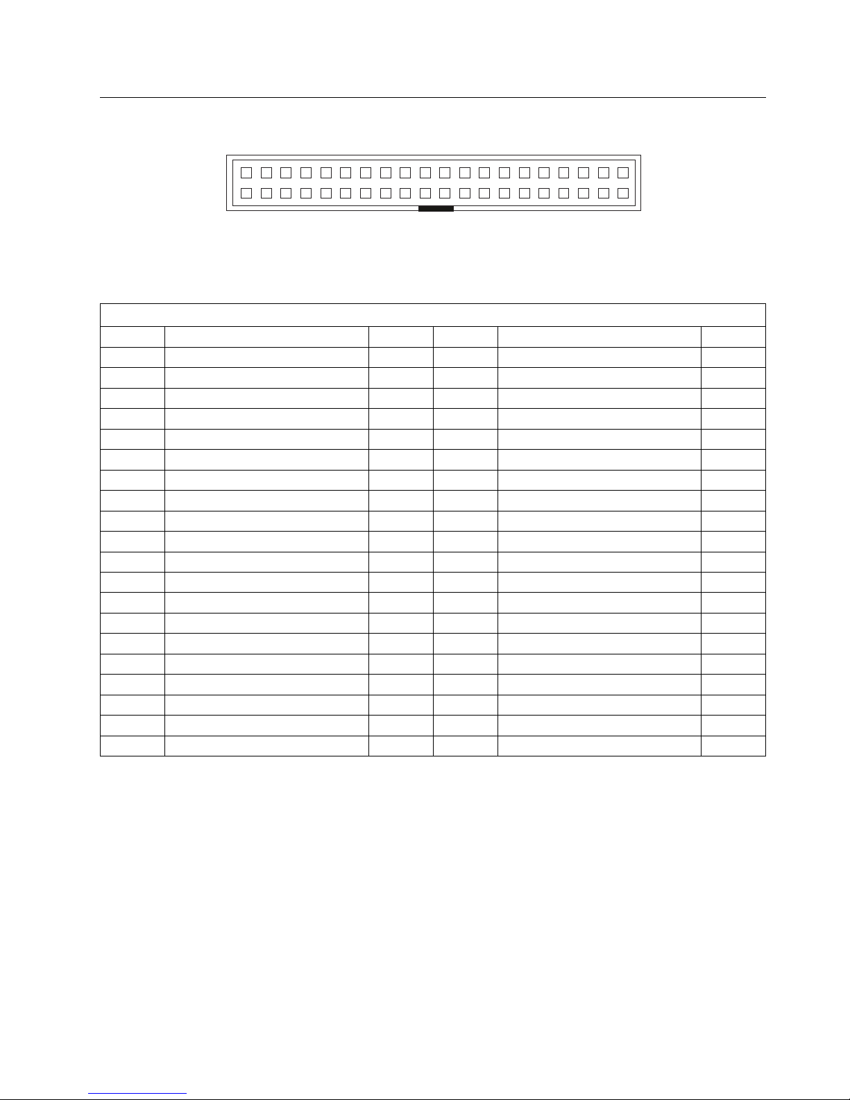
1. System Board . . . . . . . . . . . . . . . . . . . . . . . . . . . . . . . . . . . . . . . . . . . . . . . . 14
2. System Memory (DIMM) Connector .................................... 30
3. EIDE Connector . . . . . . . . . . . . . . . . . . . . . . . . . . . . . . . . . . . . . . . . . . . . . . . 33
4. Diskette Drive Connector .......................................... 34
5. Serial Port Connector ............................................ 35
6. Parallel Port Connector ........................................... 35
7. Keyboard and Mouse Port Connectors .................................. 36
8. USB Connector . . . . . . . . . . . . . . . . . . . . . . . . . . . . . . . . . . . . . . . . . . . . . . . 37
9. Infrared Port Connector ........................................... 37
10. ISA Connector . . . . . . . . . . . . . . . . . . . . . . . . . . . . . . . . . . . . . . . . . . . . . . . . 38
11. PCI Connector . . . . . . . . . . . . . . . . . . . . . . . . . . . . . . . . . . . . . . . . . . . . . . . . 40
vi Technical Information Manual
Page 9

Preface
This
Technical Information Manual
for developers who want to provide hardware and software products to operate with this IBM computer
and provides a more in-depth view of how this computer works. Users of this publication should have an
understanding of computer architecture and programming concepts.
Manual Style
provides information for the IBM PC 365 (Type 6589). It is intended
Warning: The term
Use of reserved areas can cause compatibility problems, loss of data, or permanent damage to the
hardware. When the contents of a register are changed, the state of the reserved bits must be preserved.
When possible, read the register first and change only the bits that must be changed.
In this manual, some signals are abbreviated. A minus sign in front of the signal indicates that the signal
is active low. No sign in front of the signal indicates that the signal is active high.
The use of the letter “h” indicates a hexadecimal number. Also, when numerical modifiers such as “K”,
“M” and “G” are used, they typically indicate powers of 2, not powers of 10. For example, 1 KB equals
1024 bytes (2
When expressing storage capacity, MB equals 1000 KB (1024000). The value is determined by counting
the number of sectors and assuming that every two sectors equals 1 KB.
Note: Depending on the operating system and other system requirements, the storage capacity available
to the user might vary.
10
reserved
), 1 MB equals 1 048576 bytes (220), and 1 GB equals 1073741824 bytes (230).
describes certain signals, bits, and registers that should not be changed.
Copyright IBM Corp. 1996, 1997 vii
Page 10

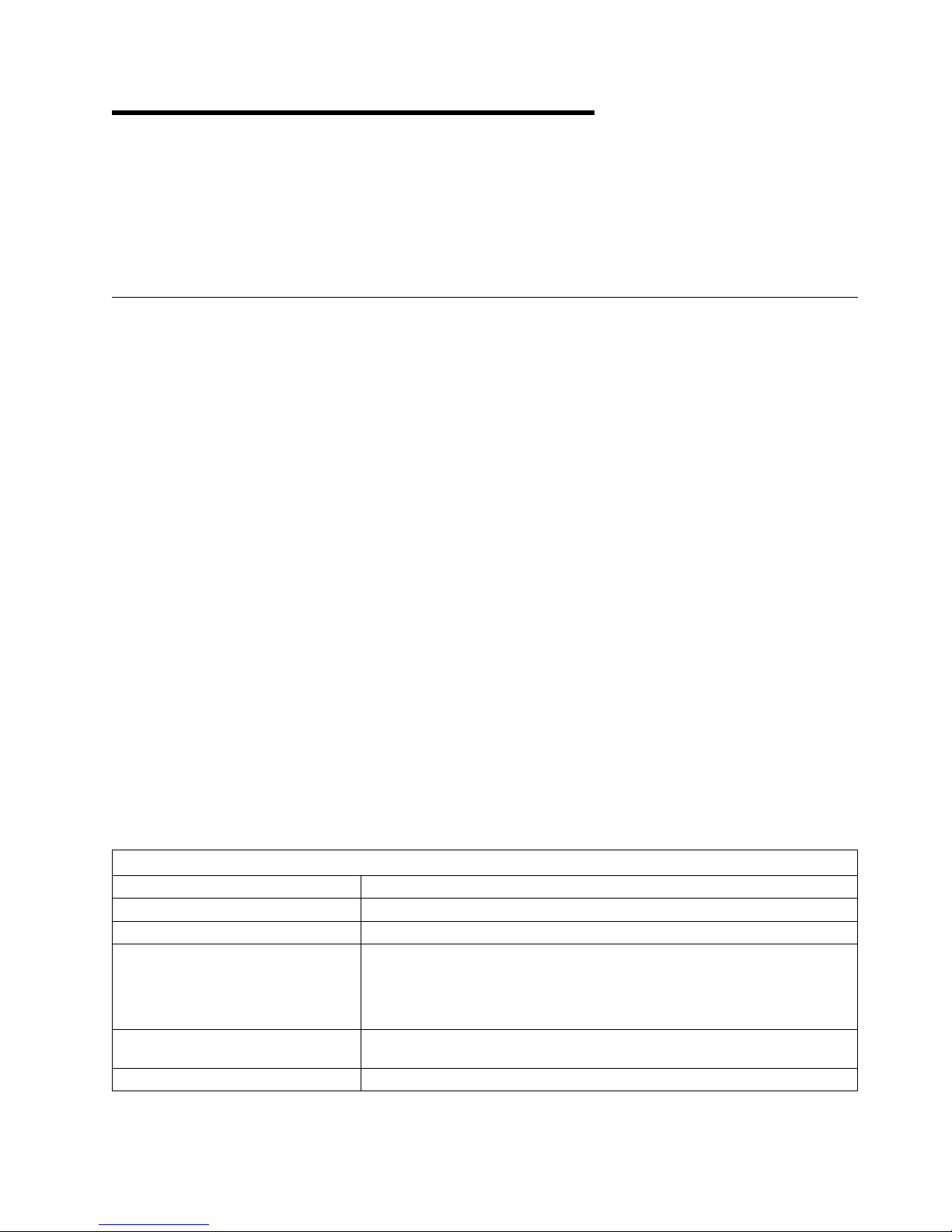
Related Publications
In addition to this manual, the following IBM publications provide information related to the operation of the
PC 365. To order publications in the U.S. and Puerto Rico, call 1-800-879-2755. In other countries,
contact an IBM reseller or an IBM marketing representative.
Using Your Personal Computer
This publication contains information about configuring, operating, and maintaining the PC 365. Also,
information on diagnosing and solving problems, how to get help and service, and warranty issues is
included.
Installing Options in Your Personal Computer
This publication contains instructions for installing options in the PC 365.
Understanding Your Personal Computer
This publication includes general information about using computers and detailed information about the
features of the PC 365.
PC 365 System (Type 6589) Compatibility Report
This publication contains information about compatible hardware and software for the PC 365. This
publication is available at
http://www.pc.ibm.com/cdt
.
S3 Trio64V+ SVGA Device Driver Installation Instructions
This publication contains instructions for installing device drivers for the S3 Trio64V+ SVGA Graphics
Adapter installed in some models.
Matrox MGA Millennium Graphics Adapter Software Installation Guide
This publication contains instructions for installing device drivers for the Matrox MGA Millennium
Graphics Adapter installed in some models. Also, this publication includes troubleshooting information
for related video problems.
Adaptec SCSI Support Package
This documentation, which is provided with models that have an IBM-installed SCSI adapter, includes
information on configuring the adapter and instructions for installing and configuring SCSI devices.
PC 365 Microprocessor Upgrade Installation Instructions
This publication contains information about installing a second Pentium Pro microprocessor on the
system board.
viii Technical Information Manual
Page 11

Chapter 1. System Overview
Chapter 1. System Overview
The IBM PC 365 (Type 6589) is a versatile product designed to provide state-of-the-art computing power
with room for future growth. Several model variations are available.
Hardware Features
Standard features in all models:
Intel Pentium Pro microprocessor with 256 KB of internal L2 cache
Dual processing support
Support for up to 512 MB of system memory
Enhanced IDE (EIDE) interface
Hard disk drive (EIDE or Fast/Wide SCSI)
One 3.5-inch, 1.44 MB diskette drive
One high-speed serial port
One high-speed parallel port
One monitor port provided with the graphics adapter
One universal serial bus port
One infrared port capable of supporting a 4 Mbps infrared transceiver
Keyboard and mouse ports
104-key keyboard and mouse provided
Standard features that vary by model:
Graphics adapter - S3 Trio64V+ SVGA Graphics Adapter
Riser card - 3 shared ISA/PCI connectors, 2 dedicated ISA connectors
connectors, 2 dedicated PCI connectors
Drive with optical media
Standard features in some models only:
Adaptec AHA-2940 Ultra Wide SCSI Adapter
Fast/Wide SCSI hard disk drive
Multimedia port for optional video features (provided with the Matrox MGA Millennium Graphics
Adapter)
1
- CD-ROM drive
or
PD/CD-ROM drive
or
Matrox MGA Millennium Graphics Adapter
or
3 shared ISA/PCI
1
Some models do not have this IBM-installed feature.
Copyright IBM Corp. 1996, 1997
1
Page 12

System Software Features
Chapter 1. System Overview
The PC 365 supports a variety of operating systems. Refer to
of supported operating systems
Note: Some models are shipped with a preloaded version of Windows NT Workstation. Also, a
Ready-to-Configure (RTC) CD-ROM is included with all models. The RTC CD-ROM has
applications and device driver support for Windows NT Workstation, Windows 95, and OS/2 Warp.
System software includes:
Basic input/output system (BIOS)
Plug and Play
Power-on self-test (POST)
Configuration/Setup Utility program
Advanced Power Management (APM)
Flash update utility program
Diagnostic programs
Using Your Personal Computer
for a listing
BIOS
The computer system uses the IBM SurePath BIOS. Enhancements to the BIOS software have been
added to provide support for the following features:
PCI bus, according to
PCI bus-master EIDE interface
Plug and Play, according to
Advanced Power Management (APM), according to
APIC (advanced programmable interrupt controls)
Multiple microprocessors, according to
Matrox video BIOS for the Matrox MGA Millennium Graphics Adapter
Bootable CD-ROM
PCI BIOS Specification 2.1
Plug and Play BIOS Specification 1.1
APM BIOS Interface Specification 1.2
Multiprocessor Specification 1.4
Plug and Play
The system conforms to the following:
Plug and Play BIOS Specification 1.1
Plug and Play BIOS Specification, Errata and Clarification 1.0
The system follows the guidelines described in the following:
Plug and Play BIOS Extension Design Guide 1.0
Guide to Integrating the Plug and Play BIOS Extensions with System BIOS 1.2
Plug and Play Kit for DOS and Windows
POST
The computer uses IBM power-on self-test (POST) software. Also, initialization code is included for the
Pentium Pro microprocessor, the 82440FX chip set, the I/O chip, and the Matrox MGA Millennium
Graphics Adapter.
POST software locates any hardware problems or configuration changes. If an error occurs while POST
is running, an error code in the form of a text message displays on the screen. For a description of a
POST error code, see “POST Error Codes” on page 48.
2 Technical Information Manual
Page 13

Chapter 1. System Overview
Configuration/Setup Utility Program
The Configuration/Setup Utility program provides menus for selecting options for devices, I/O ports, date
and time, system security, start options, advanced setup, ISA legacy resources, and power management.
More information on using the Configuration/Setup Utility program is provided in
Computer
.
Using Your Personal
Advanced Power Management
The PC 365 comes with energy-saving software that meets Energy Star requirements. Advanced Power
Management (APM) is a feature that reduces the power consumption when the entire system or
components of the computer system are not in use. When enabled, APM initiates reduced-power modes
for the monitor, microprocessor, hard disk drive, or the entire system after a specified period of inactivity is
reached.
2
APM is implemented according to
see
Using Your Personal Computer
APM BIOS Interface Specification 1.2
and
Understanding Your Personal Computer
. For more information on APM,
.
Flash Update Utility Program
The flash update utility is a stand-alone program to support flash code updates. This utility program
updates the BIOS code in flash and the MRI to different languages. The flash update utility program is
available on a 3.5-inch diskette.
Diagnostic Programs
Two diagnostic products are supplied with the PC 365: QAPlus/WIN-WIN, a Windows program, provides
the best software coverage; QAPlus/PRO for DOS provides the best hardware coverage. For more
information on these diagnostic programs, see
Using Your Personal Computer
.
2
APM does not support small computer system interface (SCSI) hard disk drives.
Chapter 1. System Overview
3
Page 14

Chapter 2. System Board Features
Chapter 2. System Board Features
This section includes information about system board features. To view an illustration of the system
board, see “System Board” on page 14.
For a list of features provided with the PC 365, see “Hardware Features” on page 1.
Microprocessor
The primary microprocessor in the PC 365 is the Intel P6, called the Pentium Pro. A voltage regulator
circuit on the system board provides the required power for the primary microprocessor. The Pentium Pro
microprocessor features:
Dynamic execution technology
Multiprocessing support
Optimization for 32-bit software
Internal L2 cache
– 4-way set associative
– Non-blocking
– 1 GB/second bandwidth communication with the microprocessor core
64-bit data bus
36-bit address bus
Upgradable to future Overdrive microprocessors
Math coprocessor
Note: Refer to
The microprocessor plugs directly into a zero-insertion-force (ZIF) socket (socket 8) on the system board.
Socket 8 allows for a performance upgrade. After an upgrade is installed, the internal speed of the
primary microprocessor is updated by setting switches on the system board (see “Switches” on page 16).
http://www.intel.com
for more information on the Intel Pentium Pro microprocessor.
Dual Processing Support
The combined technologies of the system board and the microprocessor provide support for dual
processing. The dual processing configuration is known as symmetric multiprocessing (SMP). The
PC 365 provides:
Power-supply margins for dual processing
Thermal margins for dual processing
A multiprocessor interrupt controller (for advanced programmable interrupt controls (APIC) on the
system board)
Code for APIC initialization
On the system board, directly beside the primary microprocessor, a second socket 8 is provided for
installing a second Pentium Pro microprocessor. Also, sockets are provided for connecting a
voltage-regulator module which supplies power to the second microprocessor, and a fan (part of a fan-sink
assembly), which helps cool the second microprocessor. To locate these connectors, see “System Board”
on page 14.
An upgrade kit for the PC 365 is an available option from IBM. The upgrade kit includes a Pentium Pro
microprocessor, a fan-sink assembly, a voltage-regulator module, and instructions for installation.
4 Copyright IBM Corp. 1996, 1997
Page 15

Chapter 2. System Board Features
Chip Set Control
The PC 365 uses the second-generation Intel 82440FX chip set. This chip set provides a bridge between
the peripheral component interconnect (PCI) bus and the microprocessor bus. (For information on the PCI
bus, see “PCI-to-ISA Bridge” on page 6.) Also, this chip set controls the system memory interface.
The PC 365 also uses the PIIX3 chip. This chip provides a bridge between the PCI and the industry
standard architecture (ISA) buses, a bus-master, enhanced integrated drive electronics (EIDE) interface,
and a universal serial bus (USB) port.
System Memory
Four dual inline memory module (DIMM) connectors are provided on the system board. The DIMM
connectors are powered by + 3.3 volts. Each DIMM connector is a 168-pin, gold-lead socket. For the pin
assignments, see “System Memory Connectors” on page 30.
The system board supports:
A maximum of 512 MB (128 MB modules in all four connectors).
Dynamic random access memory (DRAM) only.
64-bit (EDO) and 72-bit (ECC) wide memory modules.
Any configuration of DIMMs is acceptable. Characteristics
168-pin, unbuffered +3 V modules only.
Gold-lead tabs only.
60 nanosecond access speeds only.
Height of no more than 3.81 cm (1.5 in.).
To enable error-correcting code, all installed memory must be of the ECC type (a combination of ECC
and nonparity types is configured as nonparity)
Note: Single inline memory modules (SIMMs) are not supported in the PC 365.
required
by DIMMs include:
Chapter 2. System Board Features 5
Page 16

PCI-to-ISA Bridge
The PIIX3 chip provides the bridge between the peripheral component interconnect (PCI) and industry
standard architecture (ISA) buses. The chip is used to convert PCI bus cycles to ISA bus cycles.
Chapter 2. System Board Features
The PCI bus is compliant with
PCI Local Bus Specification 2.1
. The PCI bus runs synchronously to the
host bus and is driven at a frequency of 30 or 33 MHz, depending on the speed of the microprocessor bus
(60 MHz or 66 MHz). The ISA bus operates at speeds of 7.5 MHz or 8.33 MHz (one-quarter of the PCI
bus speed).
For information on the expansion connectors to the PCI and ISA buses, see “Riser Card” on page 13.
The following table shows the system resources used for the PCI-to-ISA bridge.
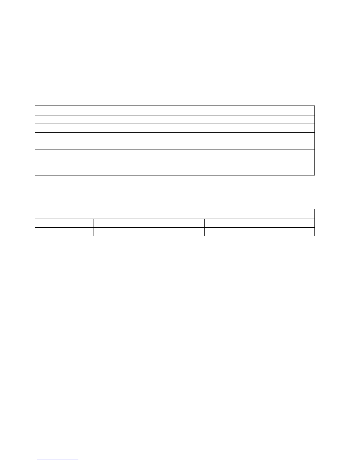
Table 1. System Resource Assignments for PCI-to-ISA Bridge
System Resource Assignment
ROM None
RAM None
I/O (hex) 00-0F, 20-43, 61, 70, 80-8F, 92, A0-BF, C0-DE, EE-F1, F4-F5
IRQ NMI, 0, 2
DMA None
Note: When the computer is started, the resource assignments are subject to change during the
power-on self-test (POST).
The chip that provides the PCI-to-ISA bridge also includes all the subsystems of the ISA bus. These
ISA-compatible subsystems are:
Two cascaded 82C59 interrupt controllers
Two 82C37 DMA controllers with four 8-bit and three 16-bit channels
Three counters equivalent to a 82C54 programmable interval timer
Power management features
6 Technical Information Manual
Page 17

Chapter 2. System Board Features
Bus Master EIDE Interface
The system board incorporates a PCI bus master, enhanced integrated drive electronics (EIDE) interface
that complies with
and EIDE buses.
The subsystem that controls internal devices is integrated with the EIDE interface. Up to four IDE devices
can be attached to the system board through a ribbon cable that connects to one of two connectors on the
system board. The IDE devices receive their power through a four-position power cable containing +5,
+12, and ground voltage.
When devices are added to the EIDE interface, one device is designated as the primary, or master, device
and another is designated as the secondary, or subordinate, device. These designations are determined
by switches or jumpers on each device. A bootable hard disk drive can be installed on either EIDE
connector.
Note: An IDE expansion adapter is not supported.
For a list of devices that might be installed in the computer, see “Internal Drives” on page 19.
The following table shows the system resources used by the EIDE interface.
AT Attachment Interface with Extensions
; this allows concurrent operations on the PCI
Table 2. System Resource Assignments for EIDE Interface
System Resource Assignment
ROM None
RAM None
I/O (hex) 170-177, 1F0-1F7, 376-377, 3F6-3F7
IRQ 14, 15
DMA None
Note: When the computer is started, the resource assignments are subject to change during the
power-on self-test (POST).
Two 40-pin connectors are provided on the system board for the EIDE interface. For information on the
pin assignments, see “EIDE Connectors” on page 33.
Chapter 2. System Board Features 7
Page 18

Chapter 2. System Board Features
USB Interface
Universal serial bus (USB) technology is a standard feature of the computer. The system board provides
the USB interface with one connector. A USB-enabled device can be attached to the connector, and if
that device is a hub, multiple peripheral devices can be attached to the hub and be used by the system.
The USB connector uses Plug and Play technology for installed devices. The speed of the USB is up to
12 Mb/second with a maximum of 255 peripheral devices.
The USB is compliant with
Universal Host Controller Interface Design Guide 1.0
. Features provided by
USB technology include:
Support for hot pluggable devices
Support for concurrent operation of multiple devices
Suitable for different device bandwidths
Connections of up to five meters in length from host to hub or hub to hub
Guaranteed bandwidth and low latencies appropriate for specific devices
Wide range of packet sizes
Limited power to hubs
The following table shows the system resources used by the USB interface.
Table 3. System Resource Assignments for USB Interface
System Resource Assignment
ROM None
RAM None
I/O (hex) Assigned by POST
IRQ Assigned by POST
DMA None
Note: When the computer is started, the resource assignments are subject to change during the
power-on self-test (POST).
At the rear of the computer, one 4-pin connector is provided for the USB interface. For information on the
pin assignments, see “USB Connector” on page 37.
8 Technical Information Manual
Page 19

Chapter 2. System Board Features
Input/Output Controller
Control of the integrated input/output (I/O) ports and diskette drive is provided by a single chip, the
National Semiconductor PC87308. This chip, which is compatible with
Specification 1.0
Diskette drive support
Serial port
Parallel port
Keyboard and mouse ports
Infrared port
General-purpose I/O ports
Real-time clock
, is a controller for the following:
Plug and Play ISA
Diskette Drive Support
The cable provided with your computer supports a maximum of two diskette drives and one tape backup
drive (see “Internal Drives” on page 19 for more information). The following is a list of devices that the
diskette drive subsystem will support:
1.44 MB, 3.5-inch diskette drive
1.2 MB, 5.25-inch diskette drive
1 Mbps, 500 Kbps, or 250 Kbps tape drive
Note: A 2.88 MB, 3.5-inch diskette drive is not supported.
One 34-pin, berg-strip connector is provided on the system board for the diskette drive. For information
on the connector pin assignments, see “Diskette Drive Connector” on page 34.
Serial Port
Two universal asynchronous receiver/transmitter (UART) serial ports are integrated into the system board.
Both ports include a 16-byte data first-in first-out (FIFO) buffer, are 16550A compatible, and have
programmable baud-rate generators.
One of the UART serial ports is used in the normal mode. The other serial port is configured as an
infrared port (see “Infrared Port” on page 10).
The following table shows the default port assignments for the serial port used in the configuration.
Table 4. Serial Port Assignments
Port Assignment Address Range IRQ Level
Serial 1 03F8h–03FFh IRQ4
Serial 2 02F8h–02FFh IRQ3
Serial 3 03E8h–03FFh IRQ4
Serial 4 02E8h–02FFh IRQ3
Note: When the computer is started, the resource assignments are subject to change during the
power-on self-test (POST).
On the system board, one 9-pin, male connector is provided for the serial port. For information on the
connector pin assignments, see “Serial Port Connector” on page 35.
Chapter 2. System Board Features 9
Page 20

Chapter 2. System Board Features
Infrared Port
Two UART serial ports are integrated into the system board. One of these ports is configured into an
infrared port. When an optional infrared module is attached to the port, the computer is capable of
transmitting and receiving wireless communications with other infrared-enable devices.
The infrared module plugs directly into the infrared port and provides a link of up to one meter. The
infrared port uses any of the same four assignments as the serial port. The infrared port is compliant with:
IrDA-2, including 4 Mbps, 1.2 Mbps, and 1.15 Mbps baud rates
Sharp-IR
TV-Remote mode
The system board has one 9-pin connector for the infrared port. For information on the connector pin
assignments for the infrared port, see “Infrared Port Connector” on page 37.
Parallel Port
Support for extended capabilities port (ECP), enhanced parallel port (EPP), and standard parallel port
(SPP) modes is integrated into the system board. The modes of operation are selected through the
Configuration/Setup Utility program with the default mode set to SPP. The ECP and EPP modes are
compliant with IEEE 1284.
The following table shows the default port assignments for the parallel port used in configuration.
Table 5. Parallel Port Assignments
Port Assignment Address Range IRQ Level
Parallel 1 03BCh–03BEh IRQ7
Parallel 2 0378h–037Fh IRQ5
Parallel 3 0278h–027Fh IRQ5
Note: When the computer is started, the resource assignments are subject to change during the
power-on self-test (POST).
On the system board, one 25-pin connector is provided for the parallel port. For information on the
connector pin assignments, see “Parallel Port Connector” on page 35.
10 Technical Information Manual
Page 21

Chapter 2. System Board Features
Keyboard and Mouse Ports
The keyboard-and-mouse subsystem is controlled by a general purpose 8-bit microcontroller. The
controller consists of 256 bytes of data memory and 2 KB of read-only memory (ROM).
The controller has two logical devices; one controls the keyboard, and the other controls the mouse. The
keyboard has two fixed I/O addresses and a fixed IRQ line and can operate without the mouse. The
mouse cannot operate without the keyboard because, although it has a fixed IRQ line, the mouse relies on
the addresses of the keyboard for operation. The following table shows the resource assignments for the
keyboard and mouse.
Table 6. System Resource Assignments for the Keyboard and Mouse
System Resource Assignment
ROM None
RAM None
I/O (hex) 60, 64
IRQ 1 (keyboard), 12 (mouse)
DMA None
Note: When the computer is started, the resource assignments are subject to change during the
power-on self-test (POST).
The system board has one 6-pin connector for the keyboard port and another 6-pin connector for the
mouse port. For information on the connector pin assignments, see “Keyboard and Mouse Port
Connectors” on page 36.
General-Purpose I/O Ports
The system board has up to 16 general-purpose input/output (GPIO) pins, which are implemented by two
8-bit GPIO ports. The use of GPIO pins is dependent upon system design. Features of the GPIO ports
are:
Open-drain outputs with internal pull-ups and transistor-transistor logic (TTL) inputs
Software-configurable base address
Programmable direction
4-byte I/O address
Chapter 2. System Board Features 11
Page 22

Chapter 2. System Board Features
Real-Time Clock
The real-time clock is a low-power clock that provides a time-of-day clock and a calendar. The clock
settings are maintained by an external battery source of +3 volts.
The system uses 242 bytes of memory to store complementary metal-oxide semiconductor (CMOS)
memory. Moving a jumper (J8) on the system board erases CMOS memory. To locate the battery or J8,
see “System Board” on page 14.
The following table shows the system resources used by the real-time clock.
Table 7. System Resource Assignments for the Real-Time Clock
System Resource Assignment
ROM None
RAM None
I/O (hex) 70, 71
IRQ 8
DMA None
Note: When the computer is started, the resource assignments are subject to change during the
power-on self-test (POST).
12 Technical Information Manual
Page 23

Chapter 2. System Board Features
Riser Card
The system board uses a riser card for expansion. The riser card plugs into the system board, and
adapters plug into the ISA-expansion or PCI-expansion connectors on the riser card. Signals from
adapters are routed to the ISA or PCI buses. Each ISA-expansion connector provides a 16-bit-wide data
path; each PCI-expansion connector provides a 32-bit-wide data path.
Each PCI-expansion connector is capable of driving one low-power Schottky load. Each ISA-expansion
connector is capable of driving two low-power Schottky loads. The ISA bus is permanently set to the PCI
bus speed divided by four.
The PCI bus shares interrupts with the ISA bus. IRQ 3, 5, 9, 10, or 11 is automatically assigned to PCI
adapters during POST. If no interrupts are available for the PCI adapters during POST, an error message
is generated.
One of two types of riser cards is used for expansion. Although both types of riser cards have five
expansion connectors, the number of dedicated PCI and ISA connectors varies. The following table
shows the characteristics of the two types of riser cards.
Table 8. Riser Card Characteristics
Expansion Connectors 5x5 Riser Card Enhanced 5x5 Riser Card
Shared ISA/PCI 3 3
Dedicated ISA 2 0
Dedicated PCI 0 2
Note: The enhanced 5x5 riser card has a PCI-to-PCI bridge chip that enables the card to support five
PCI slots.
The computer comes standard with adapters plugged into the expansion slots of the riser card. For more
information, see Chapter 3, “Adapters and Internal Drives” on page 17.
For information on the connector pin assignments, see “ISA Connectors” on page 38 and “PCI Connector”
on page 40.
Chapter 2. System Board Features 13
Page 24

Chapter 2. System Board Features
Physical Layout
The system board might look slightly different from the one shown.
Note: A diagram of the system board, including switch and jumper settings, is attached to the underside
of the computer top cover.
System Board
.1/ Parallel port connector
.2/ Universal serial bus port connector
.3/ Riser connector
.4/ Serial port connector
.5/ Mouse port connector
.6/ Keyboard port connector
.7/ J15 - Wake on LAN connector
.8/ Infrared port connector
.9/ 5 V auxiliary connector
.1ð/ J3 - Power switch connector
.11/ J8 - CMOS-clear jumper
.12/ Diskette connector
.13/ Microprocessor/diskette write-protection switches
.14/ SCSI LED connector
.15/ J13 - Wake on modem connector
.16/ J11 - Wake on modem connector
.17/ Primary EIDE connector
.18/ Secondary EIDE connector
.19/ Battery
.2ð/ Power connector
.21/ Power connector
.22/ Second microprocessor socket
.23/ Fan connector for second microprocessor
.24/ VRM connector
.25/ Primary microprocessor
.26/ J26 - Power LED connector
.27/ J30 - Front panel fan connector
.28/ System memory (DIMM) connectors
14 Technical Information Manual
Figure 1. System Board
Page 25

Chapter 2. System Board Features
Connections and the CMOS-Clear Jumper
Connections and jumpers on the system board allow custom configurations. The following tables list the
pin descriptions for specific connections and the CMOS-clear jumper. To locate these components, see
“System Board” on page 14.
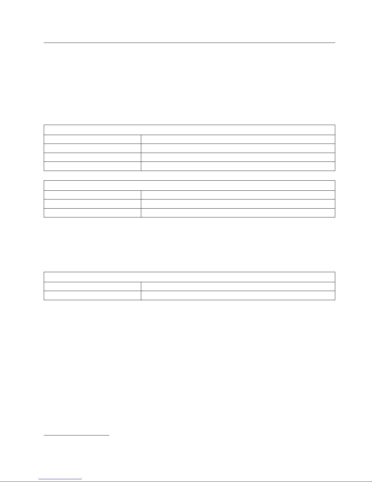
Table 9. J3 - System Power Connection
Pin Description
1 Auxiliary (+5 V dc)
2 Power switch input
Table 10. J11, J13 - Wake on Modem Ring Connections
Pin Description
1 Ground
2 Wake on Modem/Ring
Table 11. J15 - Wake on LAN Connection
Pin Description
1 Ground
2 External Wake on LAN/Ring
Table 12. J8 - CMOS-Clear Jumper
Pin Description
1 and 2 Normal
2 and 3 Clear CMOS
Chapter 2. System Board Features 15
Page 26
Switches
On the system board, a row of switches allows custom configuration of the microprocessor speed and
diskette write-protection. Refer to
accessing the switches.
After installing a microprocessor with a different speed, switches 1 through 6 are used for updating the
microprocessor speed. The following table shows the different configurations available.
Table 13. Switches 1 to 6 for Microprocessor Speeds
Switch 166 MHz 180 MHz 200 MHz 233 MHz
1 Off On On Off
2 On Off Off Off
3 On On On On
4 On On On On
5 Off On Off Off
6 On Off On On
Installing Options in Your Personal Computer
for information on
Chapter 2. System Board Features
Note: Switch 7 has no function.
The following table shows the configuration of switch 8 used for diskette write-protection.
Table 14. Switch 8 for Diskette Write-Protection
Switch Diskette Write-Enabled Diskette Write-Protected
8 Off On
16 Technical Information Manual
Page 27
Chapter 3. Adapters and Internal Drives
Chapter 3. Adapters and Internal Drives
The PC 365 comes standard with a graphics adapter and, in some models, a SCSI adapter. The
graphics adapter provides support for video, and the SCSI adapter provides an interface between the PCI
bus and SCSI devices.
Note: The IBM PCMCIA adapter for PCI or an IDE expansion adapter is not supported.
Graphics Adapters
The video subsystem is provided by one of two types of graphics adapters: the S3 Trio64V+ SVGA
Graphics Adapter or the Matrox MGA Millennium Graphics Adapter. Each adapter plugs into the riser card
and connects to the PCI bus; both adapters are compliant with
information on the riser card, see “Riser Card” on page 13.) The graphics adapters support DDC 1.1 and
DDC 2B standards.
Also, each adapter provides a 15-pin monitor connector (the Matrox MGA Millennium Graphics Adapter
also provides a multimedia connector for attaching optional video features).
PCI Local Bus Specification 2.1
. (For more
Instructions for installing device drivers for each graphics adapter are provided in
Device Driver Installation Instructions
Guide
.
and
Matrox MGA Millennium Graphics Adapter Software Installation
S3 Trio64V+ SVGA
S3 Trio64V+ SVGA Graphics Adapter
If an S3 Trio64V+ SVGA Graphics Adapter comes standard in the computer, the following major features
are provided:
2 MB of 60 ns EDO DRAM
One monitor connector
Support for all VGA modes
VESA 1.2 compliance for SVGA modes
Complete Plug and Play support
Local peripheral bus interface
The following table shows the system resources used by the S3 Trio64V+ SVGA Graphics Adapter.
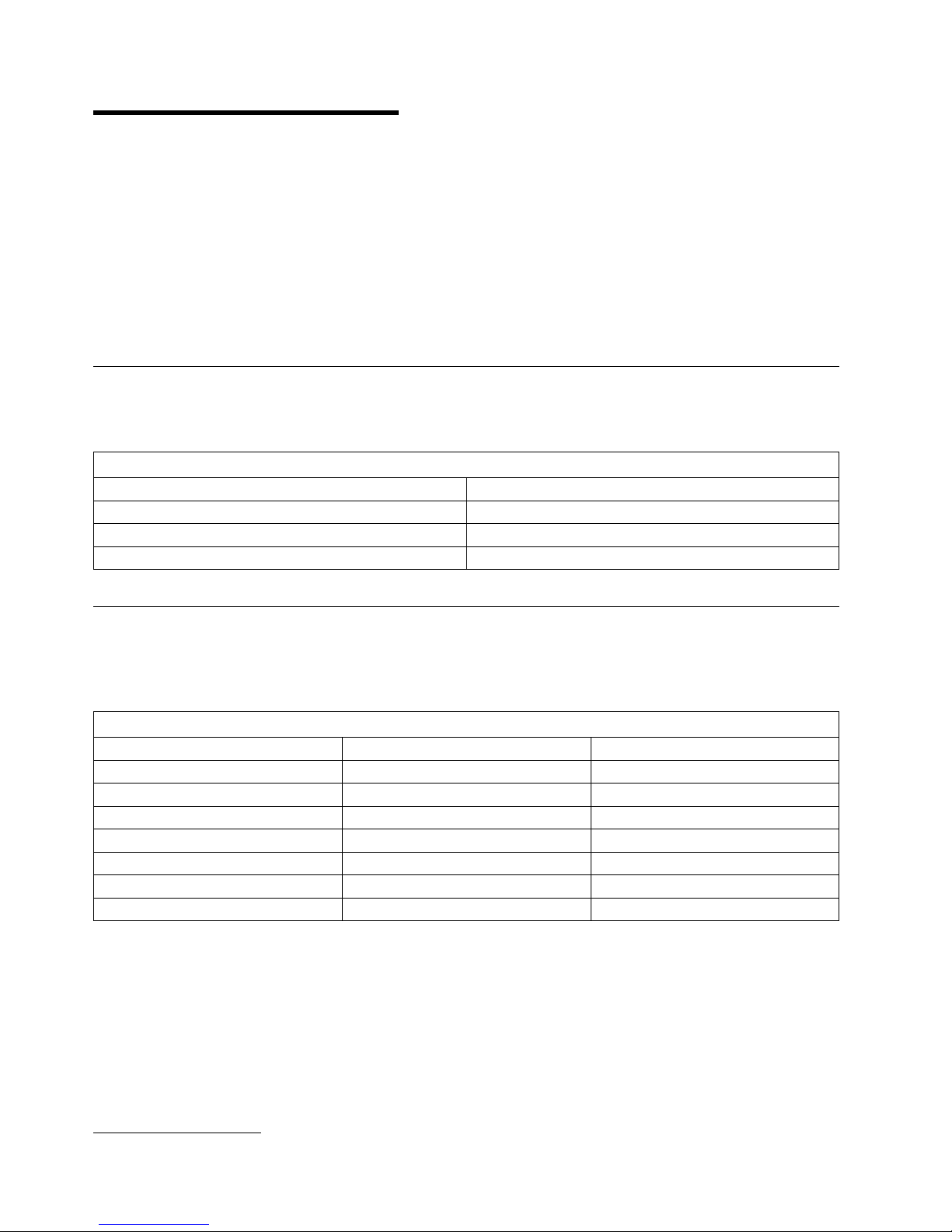
Table 15. System Resource Assignments for the S3 Trio64V+ Adapter
System Resource Assignment (hex)
ROM C0000-C7FFF (32 KB)
RAM A0000-BFFFF, (LFBBASE - (LFBBASE + 3FFFFFF)), 64 MB linear frame buffer
I/O (hex) 3B4-3B5, 3BA, 3C0-3CA, 3CC, 3CE-3CF, 3D4-3D5, 3DA, 42E8-42E9, 4AE8-4AE9,
8180-81A3, 81C0-81FF, 82E8-82EB, 86E8-86EB, 8AE8-8AEB, 8EE8-8EEB,
92E8-92EB, 96E8-96EB, 9AE8-9AEB, 9EE8-9EE9, A2E8-A2EB, A6E8-A6EB,
AAE8-AAEB, B2E8-B2EB, B6E8-B6E9, BAA38-BAE9, BEE8-BEE9, E2E8-E2EB,
EAE8-EAE9, FF00-FF37, FF40-FF5F
IRQ PCI interrupt #2 (typically assigned to ISA IRQ 9 by POST or can be disabled in the
Configuration/Setup Utility program)
DMA None
Note: When the computer is started, the resource assignments are subject to change during the
power-on self-test (POST).
Copyright IBM Corp. 1996, 1997 17
Page 28

Matrox MGA Millennium Graphics Adapter
If a Matrox MGA Millennium Graphics Adapter comes standard in the computer, the following major
features are provided:
4 MB of Windows RAM (WRAM), upgradable to 8 MB
One 15-pin monitor connector
One multimedia connector for attaching video devices
Support for all VGA modes
VESA 2.0 compliance for SVGA modes
Video POST/BIOS code
The following table shows the system resources used by the Matrox MGA Millennium Graphics Adapter.
Table 16. System Resource Assignments for the Matrox Adapter
System Resource Assignment (hex)
ROM C0000-C7FFF (32 KB)
RAM A0000-BFFFF, (MGABASE1 - (MGABASE1 + 3FFF)),
(MGABASE2 - (MGABASE2 + 7FFFFF)), 8 MB linear frame buffer
I/O (hex) 3B4-3B5, 3BA, 3C0-3C2, 3C4-3CA, 3CC, 3CE-3CF, 3D4-3D5, 3DA, 3DE-3DF
IRQ PCI interrupt #2 (typically assigned to ISA IRQ 9 by POST or can be disabled in the
Configuration/Setup Utility program)
DMA None
Chapter 3. Adapters and Internal Drives
Note: When the computer is started, the resource assignments are subject to change during the
power-on self-test (POST).
SCSI Adapter
Some models come with the Adaptec AHA-2940 Ultra Wide SCSI Adapter. This adapter provides the
interface between the PCI bus and SCSI devices. Multiple internal and external drives can be attached to
the SCSI adapter. SCSI technology is useful with multitasking operating environments because
instructions can be sent concurrently to every drive in the system. The Adaptec AHA-2940 Ultra Wide
SCSI Adapter has:
One external 68-pin, 16-bit connector
One internal 50-pin, 8-bit connector
One internal 68-pin, 16-bit connector
Up to a total of fifteen internal and external SCSI devices can be attached to the SCSI adapter, but the
number of internal devices installed is dependent upon the number of drive bays available. The PC 365
has five drive bays.
Note: A maximum of three internal SCSI hard disk drives are supported with the standard PD/CD-ROM
drive installed. A maximum of four internal hard disk drives are supported when Ultra SCSI hard
disk drives are installed.
An extra cable is provided with SCSI models. This cable provides five identical connectors for attaching
the SCSI adapter to internal SCSI devices.
For more information on connecting SCSI devices, see the
18 Technical Information Manual
Adaptec SCSI Support Package
.
Page 29
Chapter 3. Adapters and Internal Drives
Internal Drives
The EIDE, SCSI (in some models only), and diskette interfaces provide connectors for attaching internal
drives. The PC 365 comes standard with an EIDE or Fast/Wide SCSI hard disk drive, a diskette drive,
and a CD-ROM or a PD/CD-ROM drive.
Note: The appropriate device drivers are provided for the IBM-installed drives.
The following tables show the characteristics of internal drives that come standard with or are available for
the computer.
Table 17. Diskette Drives
Characteristics Number/Size
Standard One 3.5-inch, 1.44 MB
Maximum installed Three (the cable provided allows for a maximum of two diskette drives)
Optional drives 5.25-inch, 1.2 MB and 3.5-inch, 1.44 MB
Table 18. Hard Disk Drives
Characteristics Number/Size
Standard One EIDE or one Fast/Wide SCSI (size varies by model)
Maximum installed (internal) Four on the EIDE interface and four on the SCSI interface
3
Note: Although the maximum number of internal and external drives that can be connected to the SCSI
adapter is fifteen, the actual number of internal SCSI devices that can be installed is limited by the
number of available drive bays in the computer. Only three internal SCSI hard disk drives are
supported when the PD/CD-ROM drive is installed. Also, a maximum of four hard disk drives are
supported when Ultra Wide SCSI hard disk drives are installed.
Table 19. Drives with Optical Media
Characteristics Number/Size
Standard (some models only) One CD/ROM or one PD/CD-ROM4 (size varies by model)
Note: The PD/CD-ROM drive is a dual-function drive that can be used as a standard CD-ROM reader or
as an optical backup and storage device. When used as a backup and storage device, the
PD/CD-ROM drive uses a rewritable optical disk encased in a cartridge.
3
In some models, a CD-ROM or PD/CD-ROM drive is not a standard feature.
4
Both the CD/ROM and PD/CD-ROM drives connect to the EIDE interface.
Chapter 3. Adapters and Internal Drives
19
Page 30
Chapter 4. Power Supply
Chapter 4. Power Supply
Power is supplied by a 200-watt power supply that operates at either 115 V ac or 230 V ac. The voltage
setting is manually selected with a switch on the rear of the computer. The power supply converts ac
input voltages into dc output voltages and provides power for the following components:
System board
Keyboard and auxiliary ports
Riser card (ISA and PCI adapters)
Internal drives
Local area network device
Power Input
The following table shows the input power specifications.
Table 20. Power Input Requirements
Description Measurements
Input voltage, low range 90 V ac (min) to 137 V ac (max)
Input voltage, high range 180 V ac (min) to 265 V ac (max)
Input frequency 50 Hz ± 3 Hz or 60 Hz ± 3 Hz
Power Output
The power supply outputs shown in the following tables include the current supply capability of all the
connectors, including system board, internal drives, PCI, and auxiliary outputs.
Table 21. Power Output
Output Voltage Regulation Minimum to Maximum (amps)
+5 V dc +5% to −4% 1.5 to 20.0
+12 V dc +5% to −5% 0.2 to 8.0
−12 V dc +10% to −9% 0.0 to 0.5
−5 V dc +10% to −10% 0.0 to 0.5
+3.3 V dc +5% to −4% 0.0 to 20.0
+5 V dc (auxiliary) +5% to −10% 0.0 to .02
+5 V dc (Wake on LAN) +5% to −10% 0.0 to .70
5
5
5
Simultaneous loading of +3.3 V dc and +5 V dc must not exceed 120 watts.
20 Copyright IBM Corp. 1996, 1997
Page 31

Chapter 4. Power Supply
Component Outputs
The power supply provides separate voltage sources for the system board and internal storage devices.
The following tables show the approximate power that is provided for specific system components. Many
components draw less current than the maximum shown.
Table 22. System Board
Supply Voltage Maximum Current Regulation Limits
+3.3 V dc 3000 mA +5.0% to −4.0%
+5.0 V dc 4000 mA +5.0% to −4.0%
+12.0 V dc 25.0 mA +5.0% to −5.0%
−12.0 V dc 25.0 mA +10.0% to −9.0%
Table 23. Keyboard Port
Supply Voltage Maximum Current Regulation Limits
+5.0 V dc 275 mA +5.0% to −4.0%
Table 24. Auxiliary Device Port
Supply Voltage Maximum Current Regulation Limits
+5.0 V dc 300 mA +5.0% to −4.0%
Table 25. ISA-Bus Adapters (Per Slot)
Supply Voltage Maximum Current Regulation Limits
+5.0 V dc 4500 mA +5.0% to −4.0%
−5.0 V dc 200 mA +5.0% to −5.0%
+12.0 V dc 1500 mA +5.0% to −5.0%
−12.0 V dc 300 mA +10.0% to −9.0%
Table 26. PCI-Bus Adapters (Per Slot)
Supply Voltage Maximum Current Regulation Limits
+5.0 V dc 5000 mA +5.0% to −4.0%
+3.3 V dc 5000 mA +5.0% to −4.0%
Note: For each PCI connector, the maximum power consumption is rated at 25 watts for +5 V and
+3.3 V combined.
Chapter 4. Power Supply 21
Page 32

Table 27. Internal Devices (DASD)
Supply Voltage Maximum Current Regulation Limits
+5.0 V dc 1400 mA +5.0% to −5.0%
+12.0 V dc 1500 mA +5.0% to −5.0%
Note: Some adapters and hard disk drives draw more current than the recommended limits. These
adapters and drives can be installed in the system; however, the power supply will shut down if the
total power used exceeds the maximum power that is available.
Output Protection
The power supply protects against output overcurrent, overvoltage, and short circuits. Please see the
power supply specifications for details.
A short circuit that is placed on any dc output (between outputs or between an output and dc return)
latches all dc outputs into a shutdown state, with no damage to the power supply.
If this shutdown state occurs, the power supply returns to normal operation only after the fault has been
removed and the power switch has been turned off for at least one second.
Chapter 4. Power Supply
If an overvoltage fault occurs (in the power supply), the power supply latches all dc outputs into a
shutdown state before any output exceeds 130% of the nominal value of the power supply.
22 Technical Information Manual
Page 33

Chapter 4. Power Supply
Power Connectors
Note: The total power used by the any of following connectors must not exceed the amount shown in
“Component Outputs” on page 21.
The power supply provides 4-pin connectors for attaching internal devices. The following table lists the pin
assignments for these connectors.
Table 28. Pin Assignments for 4-Pin Power Connectors
Connector Location Pin 1 Pin 2 Pin 3 Pin 4
P3 3.5-inch diskette drive +5 V Ground Ground +12 V
P4 – +12 V Ground Ground +5 V
P5 DASD +12 V Ground Ground +5 V
P6 DASD +12 V Ground Ground +5 V
P7 DASD +12 V Ground Ground +5 V
P8 DASD +12 V Ground Ground +5 V
Connectors with 6 pins are used to connect the power supply to the system board and riser card. The
following table lists the pin assignments for these connectors.
Table 29. Pin Assignments for 6-Pin Power Connectors
Connector Location Pin 1 Pin 2 Pin 3 Pin 4 Pin 5 Pin 6
P1 System board Power
Good
P2 System board Ground Ground −5 V +5 V +5 V +5 V
P10 Riser 3 V +3.3 V +3.3 V +3.3 V Ground Ground Ground
P11 System board
3 V
+3.3 V +3.3 V +3.3 V Ground Ground Ground
+5 V +12 V −12 V Ground Ground
Connectors with 3 pins are provided to connect the power supply with the system board and a LAN
feature. The following table lists the pin assignments for these connectors.
Table 30. Pin Assignments for 3-Pin Power Connectors
Connector Location Pin 1 Pin 2 Pin 3
6
P9
P12 LAN +5 V Control Ground
System board +5 V Control Ground
6
AUX 5
Chapter 4. Power Supply
23
Page 34

Chapter 5. Physical Specifications
The section lists the physical specifications for the PC 365. The PC 365 has five drive bays for adding
internal drives and five expansion slots for adding adapters.
Note: The PC 365 is electromagnetically compatible with FCC Class B.
The following tables list the physical attributes.
Table 31. Size
Description Measurement
Width 420 mm (16.5 in.)
Depth 455 mm (17.9 in.)
Height 160 mm (6.3 in.)
Weight, minimum configuration 12.7 kg (28.0 lb)
Weight, maximum configuration 14.1 kg (31.0 lb)
Chapter 5. Physical Specifications
Table 32. Cables
Description Measurement
Power cable 1.63 m (5 ft 4 in.)
Keyboard cable 1.83 m (6 ft)
Ribbon cable (IDE interface) 0.51 m (1 ft 8 in.)
SCSI cable (some models only) 0.91 m (3 ft)
Table 33. Air Temperature
Description Measurement
System on 10.0 to 32.0°C (50.0 to 89.6°F)
System off 10.0 to 43.0°C (50.0 to 110.0°F)
Note: The maximum altitude at which the specified air temperatures apply is 2133.6 m (7000 ft). At
higher altitudes, the maximum air temperatures are lower than those specified.
24 Copyright IBM Corp. 1996, 1997
Page 35

Chapter 5. Physical Specifications
Table 34. Humidity
Description Measurement
System on 8% to 80%
System off 8% to 80%
Table 35. Heat Output
Description Measurement
Minimum configuration 35 W (120 Btu per hour)
Maximum configuration 204 W (700 Btu per hour)
Table 36. Electrical
Description Measurement
Low range 90 (min) to 137 (max) V ac
Low range nominal 100 to 127 V ac
High range 180 (min) to 265 (max) V ac
High range nominal 200 to 240 V ac
Frequency 50 ± 3 Hz or 60 ± 3 Hz
Input, minimum configuration 0.08 kVA
Input, maximum configuration 0.52 kVA
Chapter 5. Physical Specifications 25
Page 36

Chapter 6. System Compatibility
Chapter 6. System Compatibility
This chapter discusses some of the hardware, software, and BIOS compatibility issues for the computer.
Refer to
options.
Hardware Compatibility
This section discusses hardware and BIOS compatibility issues that must be considered when designing
application programs.
Many of the interfaces are the same as those used by the IBM Personal Computer AT. In most cases,
the command and status organization of these interfaces is maintained.
The functional interfaces are compatible with the following interfaces:
The Intel 8259 interrupt controllers (edge-triggered mode)
The National Semiconductor NS16450 and NS16550A serial communication controllers
PC 365 System (Type 6589) Compatibility Report
for a list of compatible hardware and software
The Motorola MC146818 Time of Day Clock command and status (CMOS reorganized)
The Intel 8254 timer, driven from a 1.193 MHz clock (channels 0, 1, and 2)
The Intel 8237 DMA controller, except for the Command and Request registers and the Rotate and
Mask functions; the Mode register is partially supported
The Intel 8272 or 82077 diskette drive controllers
The Intel 8042 keyboard controller at addresses 0060h and 0064h
All video standards using VGA, EGA, CGA, MDA, and Hercules modes
The parallel printer ports (Parallel 1, Parallel 2, and Parallel 3) in compatibility mode
Use the following information to develop application programs. Whenever possible, use the BIOS as an
interface to hardware to provide maximum compatibility and portability of applications among systems.
26 Copyright IBM Corp. 1996, 1997
Page 37

Chapter 6. System Compatibility
Hardware Interrupts
Hardware interrupts are level-sensitive for PCI interrupts and edge-sensitive for ISA interrupts. The
interrupt controller clears its in-service register bit when the interrupt routine sends an End of Interrupt
(EOI) command to the controller. The EOI command is sent regardless of whether the incoming interrupt
request to the controller is active or inactive.
The interrupt-in-progress latch is readable at an I/O-address bit position. This latch is read during the
interrupt service routine and might be reset by the read operation, or it might require an explicit reset.
Note: For performance and latency considerations, designers might want to limit the number of devices
sharing an interrupt level.
With level-sensitive interrupts, the interrupt controller requires that the interrupt request be inactive at the
time the EOI command is sent; otherwise, a new interrupt request will be detected. To avoid this, a
level-sensitive interrupt handler must clear the interrupt condition (usually by a read or write operation to
an I/O port on the device causing the interrupt). After processing the interrupt, the interrupt handler:
1. Clears the interrupt
2. Waits one I/O delay
3. Sends the EOI
4. Waits one I/O delay
5. Enables the interrupt through the Set Interrupt Enable Flag command
Hardware interrupt IRQ9 is defined as the replacement interrupt level for the cascade level IRQ2.
Program interrupt sharing is implemented on IRQ2, interrupt 0Ah. The following processing occurs to
maintain compatibility with the IRQ2 used by IBM Personal Computer products:
1. A device drives the interrupt request active on IRQ2 of the channel.
2. This interrupt request is mapped in hardware to IRQ9 input on the second interrupt controller.
3. When the interrupt occurs, the system microprocessor passes control to the IRQ9 (interrupt 71h)
interrupt handler.
4. This interrupt handler performs an EOI command to the second interrupt controller and passes control
to the IRQ2 (interrupt 0Ah) interrupt handler.
5. This IRQ2 interrupt handler, when handling the interrupt, causes the device to reset the interrupt
request before performing an EOI command to the master interrupt controller that finishes servicing
the IRQ2 request.
Chapter 6. System Compatibility 27
Page 38

Diskette Drives and Controller
The following tables show the reading, writing, and formatting capabilities of each type of diskette drive.
Table 37. 5.25-Inch Diskette Drive Reading, Writing, and Formatting Capabilities
Diskette Drive Type 250/500 KB Mode 300/500 KB Mode 1 MB Mode
Single sided (48 TPI) RWF — —
Double sided (48 TPI) RWF RWF —
High capacity (1.2 MB) RWF RWF RWF
Table 38. 3.5-Inch Diskette Drive Reading, Writing, and Formatting Capabilities
Diskette Drive Type 720 KB Mode 1.44 MB Mode 2.88 MB Mode
1.44 MB drive RWF RWF Not supported
Notes:
1. Do not use 5.25-inch diskettes that are designed for the 1.2 MB mode in either a 250/500 KB or
300/500 KB diskette drive.
2. Low-density 5.25-inch diskettes that are written to or formatted by a high-capacity 1.2 MB diskette
drive can be reliably read only by another 1.2 MB diskette drive.
Chapter 6. System Compatibility
Copy Protection
The following methods of copy protection might not work in systems using the 3.5-inch, 1.44 MB diskette
drive.
Bypassing BIOS routines:
– Data transfer rate: BIOS selects the proper data transfer rate for the media being used.
– Diskette parameter table: Copy protection, which creates its own diskette parameter table, might
not work in these drives.
Diskette drive controls:
– Rotational speed: The time between two events in a diskette drive is a function of the controller.
– Access time: Diskette BIOS routines must set the track-to-track access time for the different types
of media that are used in the drives.
– ‘Diskette change’ signal: Copy protection might not be able to reset this signal.
Write-current control: Copy protection that uses write-current control does not work, because the
controller selects the proper write current for the media that is being used.
Hard Disk Drives and Controller
Reading from and writing to the hard disk is initiated in the same way as in IBM Personal Computer
products; however, new functions are supported.
28 Technical Information Manual
Page 39

Chapter 6. System Compatibility
Software Compatibility
To maintain software compatibility, the interrupt polling mechanism that is used by IBM Personal Computer
products is retained. Software that interfaces with the reset port for the IBM Personal Computer
positive-edge interrupt sharing (hex address 02Fx or 06Fx, where x is the interrupt level) does not create
interference.
Software Interrupts
With the advent of software interrupt sharing, software interrupt routines must daisy-chain interrupts. Each
routine must check the function value, and if it is not in the range of function calls for that routine, it must
transfer control to the next routine in the chain. Because software interrupts are initially pointed to
address 0:0 before daisy chaining, check for this case. If the next routine is pointed to address 0:0 and
the function call is out of range, the appropriate action is to set the carry flag and do a RET 2 to indicate
an error condition.
Machine-Sensitive Programs
Programs can select machine-specific features, but they must first identify the machine and model type.
IBM has defined methods for uniquely determining the specific machine type. The machine model byte
can be found through Interrupt 15H, Return System Configuration Parameters function ((AH)=C0H).
Chapter 6. System Compatibility 29
Page 40

Appendix A. Connector Pin Assignments
The following tables show the pin assignments for various system board connectors.
System Memory Connectors
Appendix A. Connector Pin Assignments
85
1
168
84
Figure 2. System Memory (DIMM) Connector
Note: Each system memory connector is a 168-pin, gold-lead socket.
Table 39 (Page 1 of 3). 168-Pin Assignments for the System Memory Connector
Pin Signal Name I/O Pin Signal Name I/O
1 Ground NA 85 Ground NA
2 MD0 I/O 86 MD32 I/O
3 MD1 I/O 87 MD33 I/O
4 MD2 I/O 88 MD34 I/O
5 MD3 I/O 89 MD35 I/O
6 VDD I/O 90 VDD NA
7 MD4 I/O 91 MD36 NA
8 MD5 I/O 92 MD37 I/O
9 MD6 I/O 93 MD38 I/O
10 MD7 I/O 94 MD39 I/O
11 MD8 I/O 95 MD40 I/O
12 GND NA 96 Ground NA
13 MD9 I/O 97 MD41 I/O
14 MD10 I/O 98 MD42 I/O
15 MD11 O 99 MD43 I/O
16 MD12 O 100 MD44 I/O
17 MD13 O 101 MD45 I/O
18 VDD O 102 VDD NA
19 MD14 O 103 MD46 I/O
20 No connect/CB0 I/O 104 MD47 I/O
21 No connect/CB1 I/O 105 No connect/CB4 I/O
22 PAR2 I/O 106 No connect/CB5 I/O
23 Ground I/O 107 Ground NA
24 No connect NA 108 No connect NA
25 No connect NA 109 No connect NA
26 VDD O 110 VDD NA
27 WE0 O 111 DU NA
28 CAS0 O 112 CAS4 O
30 Copyright IBM Corp. 1996, 1997
Page 41

Appendix A. Connector Pin Assignments
Table 39 (Page 2 of 3). 168-Pin Assignments for the System Memory Connector
Pin Signal Name I/O Pin Signal Name I/O
29 CAS1 O 113 CAS5 O
30 RAS0 O 114 RAS1 O
31 OE0 O 115 DU NA
32 Ground O 116 Ground NA
33 A0 O 117 A1 O
34 A2 O 118 A3 O
35 A4 O 119 A5 O
36 A6 O 120 A7 O
37 A8 O 121 A9 O
38 A10 O 122 A11 O
39 A12 O 123 A13 O
40 VDD NA 124 VDD NA
41 No connect NA 125 DU NA
42 No connect (DU) NA 126 DU NA
43 Ground NA 127 Ground NA
44 OE2 O 128 DU NA
45 RAS2 O 129 RAS3 O
46 CAS2 O 130 CAS6 O
47 CAS3 O 131 CAS7 O
48 WE2 O 132 DU NA
49 VDD O 133 VDD NA
50 No connect NA 134 No connect NA
51 No connect NA 135 No connect NA
52 No connect/CB2 I/O 136 No connect/CB6 I/O
53 No connect/CB3 I/O 137 No connect/CB7 I/O
54 Ground NA 138 Ground NA
55 MD16 I/O 139 MD48 I/O
56 MD17 I/O 140 MD49 I/O
57 MD18 I/O 141 MD50 I/O
58 MD19 I/O 142 MD51 I/O
59 VDD NA 143 VDD NA
60 MD20 I/O 144 MD52 I/O
61 No connect NA 145 No connect NA
62 DU NA 146 DU NA
63 No connect NA 147 No connect NA
64 Ground NA 148 Ground NA
65 MD21 I/O 149 MD53 I/O
66 MD22 I/O 150 MD54 I/O
67 MD23 I/O 151 MD55 I/O
68 Ground NA 152 Ground NA
69 MD24 I/O 153 MD56 I/O
70 MD25 I/O 154 MD57 I/O
71 MD26 I/O 155 MD58 I/O
Appendix A. Connector Pin Assignments 31
Page 42

Table 39 (Page 3 of 3). 168-Pin Assignments for the System Memory Connector
Pin Signal Name I/O Pin Signal Name I/O
72 MD27 I/O 156 MD59 I/O
73 VDD NA 157 VDD NA
74 MD28 I/O 158 MD60 I/O
75 MD29 I/O 159 MD61 I/O
76 MD30 I/O 160 MD62 I/O
77 MD31 I/O 161 MD63 I/O
78 Ground NA 162 Ground NA
79 No connect I/O 163 No connect NA
80 No connect I/O 164 No connect NA
81 No connect I/O 165 SA0 I/O
82 SDA I/O 166 SA1 I/O
83 SCL I/O 167 SA2 I/O
84 VDD NA 168 VDD I/O
Appendix A. Connector Pin Assignments
32 Technical Information Manual
Page 43
Appendix A. Connector Pin Assignments
EIDE Connectors
2
1
40
39
Figure 3. EIDE Connector
Note: Each EIDE connector is a 40-pin, shrouded berg strip.
Table 40. 40-Pin Assignments for the EIDE Connectors
Pin Signal Name I/O Pin Signal Name I/O
1 Reset O 2 Ground NA
3 D7 I/O 4 D8 I/O
5 D6 I/O 6 D9 I/O
7 D5 I/O 8 D10 I/O
9 D4 I/O 10 D11 I/O
11 D3 I/O 12 D12 I/O
13 D2 I/O 14 D13 I/O
15 D1 I/O 16 D14 I/O
17 D0 I/O 18 D15 I/O
19 Ground NA 20 Key connector NA
21 No connect NA 22 Ground NA
23 IOW# O 24 No connect NA
25 IOR# O 26 Ground NA
27 IOCHRDY I 28 ALE O
29 No connect NA 30 Ground NA
31 IRQ I 32 CS16# I
33 SA1 O 34 PDIAG I
35 SA0 O 36 SA2 O
37 CS0# O 38 CS1 O
39 Active# I 40 Ground NA
Appendix A. Connector Pin Assignments 33
Page 44

Diskette Drive Connector
Appendix A. Connector Pin Assignments
2
1
34
33
Figure 4. Diskette Drive Connector
Note: The connector for the diskette drive is a 34-pin, berg strip.
Table 41. 34-Pin Assignments for the Diskette Drive Connector
Pin Signal Name I/O Pin Signal Name I/O
1 Reserved I 2 High density select O
3 Not connected NA 4 Not connected NA
5 Ground NA 6 Data rate 0 NA
7 Ground NA 8 Index# I
9 Reserved NA 10 Motor enable 0 O
11 Ground NA 12 Drive select 1 O
13 Ground NA 14 Drive select 0 O
15 Ground NA 16 Motor enable 1 O
17 MSEN1 I 18 Direction in# O
19 Ground NA 20 Step# O
21 Ground NA 22 Write data# O
23 Ground NA 24 Write enable# O
25 Ground NA 26 Track0# I
27 MSEN0 I 28 Write protect# I
29 Ground NA 30 Read data# I
31 Ground NA 32 Head 1 select# O
33 Data rate 1 NA 34 Diskette change# I
34 Technical Information Manual
Page 45
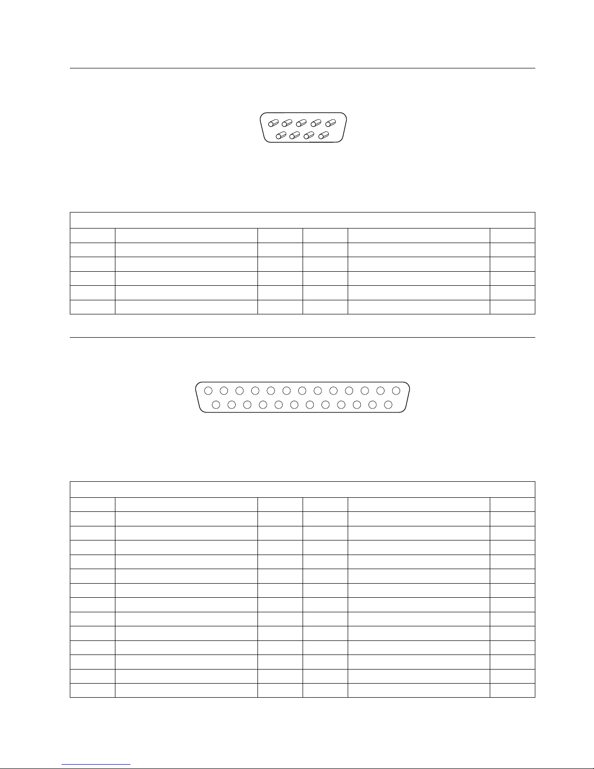
Appendix A. Connector Pin Assignments
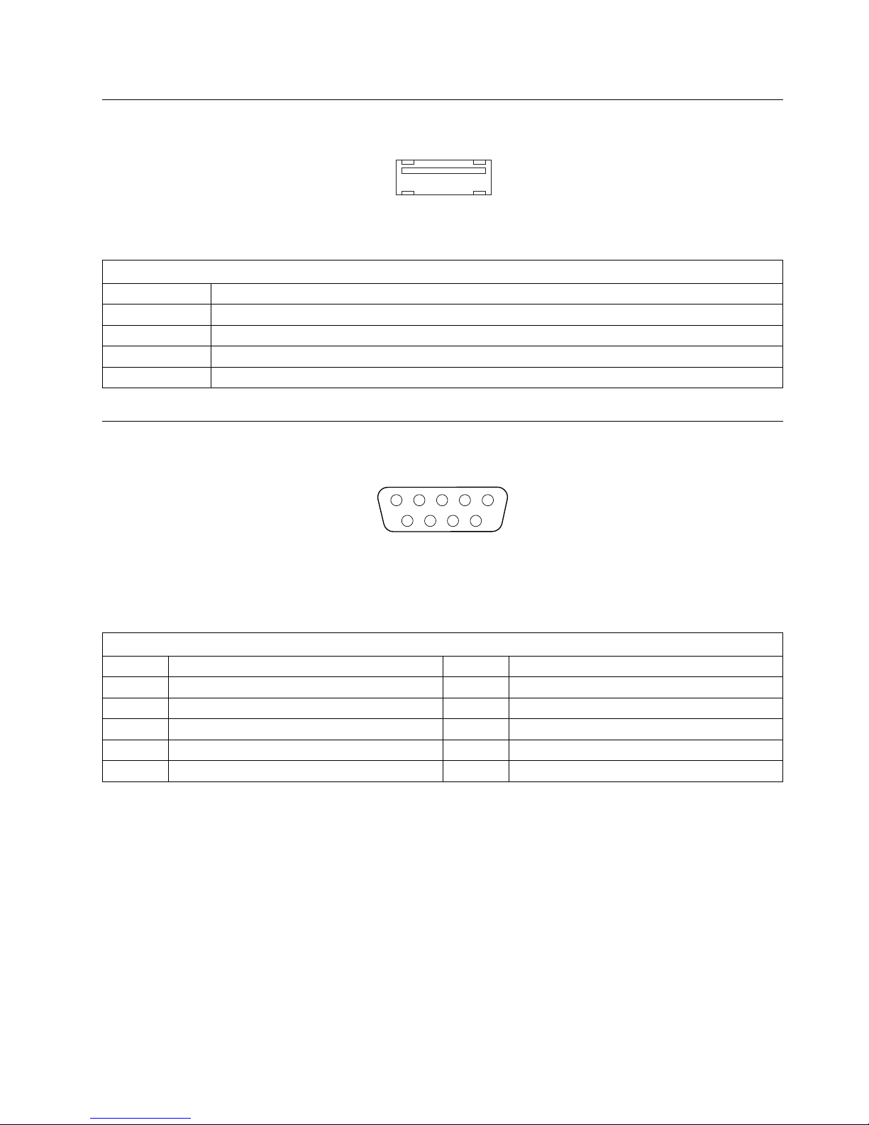
Serial Port Connector
1
5
69
Figure 5. Serial Port Connector
Note: The external interface for the serial port is a male, 9-pin D-shell connector.
Table 42. 9-Pin Assignments for the Serial Port Connector
Pin Signal Name I/O Pin Signal Name I/O
1 Data carrier detect I 2 Receive data# I
3 Transmit data# O 4 Data terminal read O
5 Ground NA 6 Data set ready I
7 Request to send O 8 Clear to send I
9 Ring indicator I
Parallel Port Connector
13
1
25 14
Figure 6. Parallel Port Connector
Note: The external interface for the parallel port is a female, 25-pin D-shell connector.
Table 43. 25-Pin Assignments for the Parallel Port Connector
Pin Signal Name I/O Pin Signal Name I/O
1 STROBE# I/O 2 D0 I/O
3 D1 I/O 4 D2 I/O
5 D3 I/O 6 D4 I/O
7 D5 I/O 8 D6 I/O
9 D7 I/O 10 ACK# I
11 BUSY I 12 PE I
13 SLCT I 14 AUTO FD XT# O
15 ERROR# I 16 INIT# O
17 SLCT IN# O 18 Ground NA
19 Ground NA 20 Ground NA
21 Ground NA 22 Ground NA
23 Ground NA 24 Ground NA
25 Ground NA
Appendix A. Connector Pin Assignments 35
Page 46
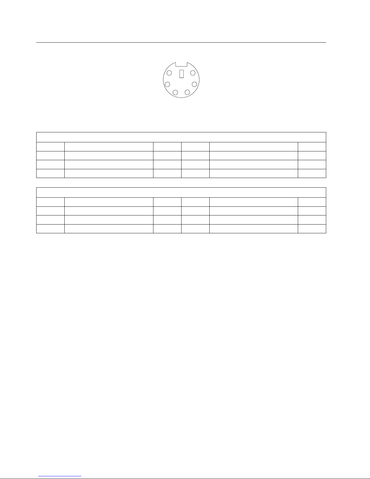
Keyboard and Mouse Port Connectors
6
5
3
4
1
2
Figure 7. Keyboard and Mouse Port Connectors
Note: The external interface for the keyboard and mouse ports are 6-pin, mini-DIN connectors.
Table 44. 6-Pin Assignments for the Keyboard Connector
Pin Signal Name I/O Pin Signal Name I/O
1 Data I/O 2 Aux data I/O
3 Ground NA 4 +5 V dc NA
5 Clock I/O 6 Aux clock I/O
Appendix A. Connector Pin Assignments
Table 45. 6-Pin Assignments for the Mouse Connector
Pin Signal Name I/O Pin Signal Name I/O
1 Data I/O 2 Reserved NA
3 Ground NA 4 +5 V dc NA
5 Clock I/O 6 Reserved NA
36 Technical Information Manual
Page 47
Appendix A. Connector Pin Assignments
USB Connector
Figure 8. USB Connector
Table 46. 4-Pin Assignments for the USB Connector
Pin Signal Name
1 VCC
2 -Data
3 +Data
4 Ground
Infrared Port Connector
1
3
1
2
4
5
69
Figure 9. Infrared Port Connector
Note: The external interface for the infrared port is a female, 9-pin D-shell connector.
Table 47. 9-Pin Assignments for the Infrared Connector
Pin Signal Name Pin Signal Name
1 IR transmitted data (output) 2 Ground
3 Reserved 4 IR module select 2
5 IR module select 1 6 IR received data (input)
7 Voltage (+5 V dc) 8 IR module select 0
9 No connect
Appendix A. Connector Pin Assignments 37
Page 48

ISA Connectors
Appendix A. Connector Pin Assignments
A1
B1
B31 D1
C18A31 C1
D18
Figure 10. ISA Connector
Note: The ISA connectors are part of the riser card.
Table 48 (Page 1 of 2). 98-Pin Assignments for the ISA Connector
Pin Signal Name I/O Pin Signal Name I/O
B1 Ground NA A1 IOCHCK# I
B2 RESET DRV O A2 SD7 I/O
B3 +5 V dc NA A3 SD6 I/O
B4 IRQ2 I A4 SD5 I/O
B5 −5 V dc NA A5 SD4 I/O
B6 DRQ2 I A6 SD3 I/O
B7 −12 V dc NA A7 SD2 I/O
B8 OWS# I A8 SD1 I/O
B9 +12 V dc NA A9 SD0 I/O
B10 Ground NA A10 IOCHRDY I
B11 SMEMW# O A11 AEN O
B12 SMEMR# O A12 SA19 I/O
B13 IOW# I/O A13 SA18 I/O
B14 IOR# I/O A14 SA17 I/O
B15 DACK3# O A15 SA16 I/O
B16 DRQ3 I A16 SA15 I/O
B17 DACK1# O A17 SA14 I/O
B18 DRQ1 I A18 SA13 I/O
B19 REFRESH# I/O A19 SA12 I/O
B20 CLK O A20 SA11 I/O
B21 IRQ7 I A21 SA10 I/O
B22 IRQ6 I A22 SA9 I/O
B23 IRQ5 I A23 SA8 I/O
B24 IRQ4 I A24 SA7 I/O
B25 IRQ3 I A25 SA6 I/O
B26 DACK2# O A26 SA5 I/O
B27 TC O A27 SA4 I/O
B28 BALE O A28 SA3 I/O
B29 +5 V dc NA A29 SA2 I/O
B30 OSC O A30 SA1 I/O
B31 Ground NA A31 SA0 I/O
D1 MEMCS16# I C1 SBHE# I/O
38 Technical Information Manual
Page 49

Appendix A. Connector Pin Assignments
Table 48 (Page 2 of 2). 98-Pin Assignments for the ISA Connector
Pin Signal Name I/O Pin Signal Name I/O
D2 IOCS16# I C2 LA23 I/O
D3 IRQ10 I C3 LA22 I/O
D4 IRQ11 I C4 LA21 I/O
D5 IRQ12 I C5 LA20 I/O
D6 IRQ15 I C6 LA19 I/O
D7 IRQ14 I C7 LA18 I/O
D8 DACK0# O C8 LA17 I/O
D9 DRQ0 I C9 MEMR# I/O
D10 DACK5# O C10 MEMW# I/O
D11 DRQ5 I C11 SD8 I/O
D12 DACK6# O C12 SD9 I/O
D13 DRQ6 I C13 SD10 I/O
D14 DACK7# O C14 SD11 I/O
D15 DRQ7 I C15 SD12 I/O
D16 +5 V dc NA C16 SD13 I/O
D17 MASTER# I C17 SD14 I/O
D18 Ground NA C18 SD15 I/O
Appendix A. Connector Pin Assignments 39
Page 50

PCI Connector
Appendix A. Connector Pin Assignments
A1
B1
B49 B52
A62A49 A52
B62
Figure 11. PCI Connector
Note: The PCI connectors are part of the riser card.
Table 49 (Page 1 of 2). 124-Pin Assignments for the PCI Connector
Pin Signal Name I/O Pin Signal Name I/O
A1 TRST# O B1 −12 V dc NA
A2 +12 V dc dc NA B2 TCK O
A3 TMS O B3 Ground NA
A4 TDI O B4 TDO I
A5 +5 V dc NA B5 +5 V dc NA
A6 INTA# I B6 +5 V dc NA
A7 INTC# I B7 INTB# I
A8 +5 V dc NA B8 INTD# I
A9 Reserved NA B9 PRSNT1# I
A10 +5 V dc (I/O) NA B10 Reserved NA
A11 Reserved NA B11 PRSNT2 I
A12 Ground NA B12 Ground NA
A13 Ground NA B13 Ground NA
A14 Reserved NA B14 Reserved NA
A15 RST# O B15 Ground NA
A16 +5 V dc (I/O) NA B16 CLK O
A17 GNT# O B17 Ground NA
A18 Ground NA B18 REQ# I
A19 Reserved NA B19 +5 V dc (I/O) NA
A20 Address/Data 30 I/O B20 Address/Data 31 I/O
A21 +3.3 V dc NA B21 Address/Data 29 I/O
A22 Address/Data 28 I/O B22 Ground NA
A23 Address/Data 26 I/O B23 Address/Data 27 I/O
A24 Ground NA B24 Address/Data 25 I/O
A25 Address/Data 24 I/O B25 +3.3 V dc NA
A26 IDSEL O B26 C/BE 3# I/O
A27 +3.3 V dc NA B27 Address/Data 23 I/O
A28 Address/Data 22 I/O B28 Ground NA
A29 Address/Data 20 I/O B29 Address/Data 21 I/O
A30 Ground NA B30 Address/Data 19 I/O
A31 Address/Data 18 I/O B31 +3.3 V dc NA
A32 Address/Data 16 I/O B32 Address/Data 17 I/O
A33 +3.3 V dc NA B33 C/BE 2# I/O
40 Technical Information Manual
Page 51

Appendix A. Connector Pin Assignments
Table 49 (Page 2 of 2). 124-Pin Assignments for the PCI Connector
Pin Signal Name I/O Pin Signal Name I/O
A34 FRAME# I/O B34 Ground NA
A35 Ground NA B35 IRDY# I/O
A36 TRDY# I/O B36 +3.3 V dc NA
A37 Ground NA B37 DEVSEL# I/O
A38 STOP# I/O B38 Ground NA
A39 +3.3 V dc NA B39 LOCK# I/O
A40 SDONE I/O B40 PERR# I/O
A41 SBO# I/O B41 +3.3 V dc NA
A42 Ground NA B42 SERR# I/O
A43 +3.3 V dc NA B43 +3.3 V dc NA
A44 C/BE(1)# I/O B44 C/BE 1# I/O
A45 Address/Data 14 I/O B45 Address/Data 14 I/O
A46 Ground NA B46 Ground NA
A47 Address/Data 12 I/O B47 Address/Data 12 I/O
A48 Address/Data 10 I/O B48 Address/Data 10 I/O
A49 Ground NA B49 Ground NA
A50 Key NA B50 Key NA
A51 Key NA B51 Key NA
A52 Address/Data 8 I/O B52 Address/Data 8 I/O
A53 Address/Data 7 I/O B53 Address/Data 7 I/O
A54 +3.3 V dc NA B54 +3.3 V dc NA
A55 Address/Data 5 I/O B55 Address/Data 5 I/O
A56 Address/Data 3 I/O B56 Address/Data 3 I/O
A57 Ground NA B57 Ground NA
A58 Address/Data 1 I/O B58 Address/Data 1 I/O
A59 +5 V dc (I/O) NA B59 +5 V dc (I/O) NA
A60 ACK64# I/O B60 ACK64# I/O
A61 +5 V dc NA B61 +5 V dc NA
A62 +5 V dc NA B62 +5 V dc NA
Appendix A. Connector Pin Assignments 41
Page 52

Appendix B. System Address Maps
System Memory Map
Memory can be mapped differently if POST detects an error.
Table 50. System Memory Map
Address Range (hex) Size Description
00000000–0007FFFF 512 KB DOS applications
640 KB Memory gap
768 KB Video buffer
1 MB Expansion and BIOS region
15 MB Cacheable
16 MB Optional memory space gap
512 MB Always cacheable
FEC00000–FEC01000 4 KB I/O APIC default
FEE00000–FE010000 4 KB APIC default
FFF80000–FFFDF000 384 KB Extended BIOS
FFFE0000–FFFFFFFF 128 KB BIOS memory shadowed
Appendix B. System Address Maps
42 Copyright IBM Corp. 1996, 1997
Page 53

Appendix B. System Address Maps
Input/Output Address Map
The following table lists resource assignments for the I/O address map. Any addresses that are not
shown are reserved.
Table 51. I/O Address Map
Address (Hex) Device
0000–000F DMA 1
0020–0021 Interrupt controller 1
0040–0043 Timer 1
0048–004B Timer 2
0060 Keyboard controller data byte
0061 NMI, speaker control
0064 Keyboard controller command/status byte
0070, bit 7 Enable NMI
0070, bits 6:0 Real-time clock, address
0071 Real-time clock, data
0078 Reserved (system board configuration)
007C Reserved (system board configuration)
0080–008F DMA page register
00A0–00A1 Interrupt controller 2
00C0–00DE DMA 2
00F0 Reset numeric error
0170–0177 Secondary IDE channel
01F0–01F7 Primary IDE channel
0278–027B Parallel port 2
02F8–02FF Onboard serial port 2
0376 Secondary IDE channel command port
0377 Secondary IDE channel status port
0378–037F Parallel port 1
03BC–03BF Parallel port x
03E8–03EF Serial port 3
03F0–03F5 Diskette channel 1
03F6 Primary IDE channel command port
03F7 (Write) Diskette channel 1 command
03F7, bit 7 Diskette change channel 1
03F7, bits 6:0 Primary IDE channel status port
03F8–03FF Onboard serial port 1
LPT + 400h ECP port, LPT + 400h
0CF8–0CFB PCI configuration address register
0CFC–0CFF PCI configuration data register
FF00–FF07 IDE bus master register
Appendix B. System Address Maps 43
Page 54

DMA I/O Address Map
The following table lists resource assignments for the DMA address map. Any addresses that are not
shown are reserved.
Table 52 (Page 1 of 2). DMA I/O Addresses
Address (Hex) Description Bits Byte Pointer
0000 Channel 0, Memory Address register 00–15 Yes
0001 Channel 0, Transfer Count register 00–15 Yes
0002 Channel 1, Memory Address register 00–15 Yes
0003 Channel 1, Transfer Count register 00–15 Yes
0004 Channel 2, Memory Address register 00–15 Yes
0005 Channel 2, Transfer Count register 00–15 Yes
0006 Channel 3, Memory Address register 00–15 Yes
0007 Channel 3, Transfer Count register 00–15 Yes
0008 Channels 0–3, Read Status/Write Command register 00–07
0009 Channels 0–3, Write Request register 00–02
000A Channels 0–3, Write Single Mask register bits 00–02
000B Channels 0–3, Mode register (write) 00–07
000C Channels 0–3, Clear byte pointer (write) NA
000D Channels 0–3, Master clear (write)/temp (read) 00–07
000E Channels 0–3, Clear Mask register (write) 00–03
000F Channels 0–3, Write All Mask register bits 00–03
0081 Channel 2, Page Table Address register
0082 Channel 3, Page Table Address register
0083 Channel 1, Page Table Address register
0087 Channel 0, Page Table Address register
0089 Channel 6, Page Table Address register
008A Channel 7, Page Table Address register
008B Channel 5, Page Table Address register
008F Channel 4, Page Table Address/Refresh register 00–07
00C0 Channel 4, Memory Address register 00–15 Yes
00C2 Channel 4, Transfer Count register 00–15 Yes
00C4 Channel 5, Memory Address register 00–15 Yes
00C6 Channel 5, Transfer Count register 00–15 Yes
00C8 Channel 6, Memory Address register 00–15 Yes
00CA Channel 6, Transfer Count register 00–15 Yes
00CC Channel 7, Memory Address register 00–15 Yes
00CE Channel 7, Transfer Count register 00–15 Yes
00D0 Channels 4–7, Read Status/Write Command register 00–07
00D2 Channels 4–7, Write Request register 00–02
00D4 Channels 4–7, Write Single Mask register bit 00–02
00D6 Channels 4–7, Mode register (write) 00–07
00D8 Channels 4–7, Clear byte pointer (write) NA
00DA Channels 4–7, Master clear (write)/temp (read) 00–07
7
7
7
7
7
7
7
00–07
00–07
00–07
00–07
00–07
00–07
00–07
Appendix B. System Address Maps
44 Technical Information Manual
Page 55

Appendix B. System Address Maps
Table 52 (Page 2 of 2). DMA I/O Addresses
Address (Hex) Description Bits Byte Pointer
00DC Channels 4–7, Clear Mask register (write) 00–03
00DE Channels 4–7, Write All Mask register bits 00–03
00DF Channels 5–7, 8- or 16-bit mode select 00–07
7
Upper byte of memory address register.
Appendix B. System Address Maps
45
Page 56

Appendix C. IRQ and DMA Channel Assignments
The following tables list the interrupt request (IRQ) and direct memory access (DMA) channel
assignments.
Table 53. IRQ Channel Assignments
IRQ System Resource
NMI Critical system error
SMI System/power management interrupt
0 Reserved (internal timer)
1 Reserved (keyboard)
2 Reserved (interrupt controller) timer in APIC mode
8
3
8
4
Infrared
Serial port
5 Available
6 Diskette
8
7
Parallel port
8 Real-time clock
9 Available
10 Available
11 Available
8
12
Mouse
13 Coprocessor
14 IDE drives (0, 1) if installed
15 IDE drives (2, 3) if installed
9
Appendix C. IRQ and DMA Channel Assignments
8
Can be modified to alternate settings or disabled.
9
With dual processing, the advanced programmable interrupt controller (APIC) manages hardware interrupts to the system BIOS.
The following interrupts are available only in the dual-processing APIC mode.
IRQ System Resource
16 PCI device
17 PCI device
18 PCI device
19 PCI device
20 Not available
21 Not available
22 Not available
23 Not available
24 SMI
46 Copyright IBM Corp. 1996, 1997
Page 57

Appendix C. IRQ and DMA Channel Assignments
Table 54. DMA Channel Assignments
DMA Channel Data Width System Resource
0 Available 8 bits
1 Infrared
2 Reserved (diskette drive) 8 bits
3 Parallel port
4 Available –
5 Available 16 bits
6 Available 16 bits
7 Available 16 bits
10
10
8 bit
8 bits
10
Can be modified to alternative settings or disabled.
Appendix C. IRQ and DMA Channel Assignments
47
Page 58

Appendix D. Error Codes
Appendix D. Error Codes
The following tables list the POST error codes and beep error codes for the computer.
POST Error Codes
POST error messages appear when POST finds problems with the hardware during power-on or when a
change in the hardware configuration is found. POST error messages are 3-, 4-, 5-, 8-, or 12-character
alphanumeric messages. An x in an error message can represent any number.
Table 55 (Page 1 of 2). POST Error Codes
Code Description
101 Interrupt failure
102 Timer failure
103 Timer-interrupt failure
104 Protected mode failure
105 Last 8042 command not accepted – keyboard failure
106 System board failure
108 Timer bus failure
109 Low MB chip select test
110 System board parity error 1 (system board parity latch set)
111 I/O parity error 2 (I/O channel check latch set)
112 I/O channel check error
113 I/O channel check error
114 External ROM checksum error
115 DMA error
116 System board port read/write error
120 Microprocessor test error
121 Hardware error
151 Real time clock failure
161 Bad CMOS Battery
162 CMOS RAM checksum/configuration error
163 Clock not updating
164 CMOS RAM memory size does not match
167 Clock not updating
175 Riser card or system board error
176 System cover has been removed
177 Corrupted administrator password
178 Riser card or system board error
183 Administrator password has been set and must be entered
184 Password removed due to checksum error
185 Corrupted boot sequence
186 System board or hardware security error
189 More than three password attempts were made to access system
201 Memory data error
48 Copyright IBM Corp. 1996, 1997
Page 59

Appendix D. Error Codes
Table 55 (Page 2 of 2). POST Error Codes
Code Description
202 Memory address line error 00-15
203 Memory address line error 16-23
221 ROM to RAM remapping error
225 Unsupported memory type installed or memory pair mismatch
301 Keyboard error
302 Keyboard error
303 Keyboard to system board interface error
304 Keyboard clock high
305 No keyboard +5Vdc
601 Diskette drive or controller error
602 Diskette IPL boot record not valid
604 Unsupported diskette drive installed
605 POST cannot unlock diskette drive
662 Diskette drive configuration error
762 Math coprocessor configuration error
11xx Serial port error (xx = serial port number)
1762 Hard disk configuration error
1780 Hard disk 0 failed
1781 Hard disk 1 failed
1782 Hard disk 2 failed
1783 Hard disk 3 failed
1800 PCI adapter has requested an unavailable hardware interrupt
1801 PCI adapter has requested an unavailable memory resource
1802 PCI adapter has requested an unavailable I/O address space, or a defective adapter
1803 PCI adapter has requested an unavailable memory address space, or a defective adapter
1804 PCI adapter has requested unavailable memory addresses
1805 PCI adapter ROM error
1962 Boot sequence error
2401 System board video error
8601 System board - keyboard/pointing device error
8602 Pointing device error
8603 Pointing device or system board error
12092 Level 1 cache error (Processor chip)
12094 Level 2 cache error
I9990301 Hard disk failure
I9990305 No operating system found
Appendix D. Error Codes 49
Page 60

Appendix D. Error Codes
Beep Codes
For the following beep codes, the numbers indicate the sequence and number of beeps. For example, a
“2-3-2” error symptom (a burst of two beeps, three beeps, then two beeps) indicates a memory module
problem. An x in an error message can represent any number.
Table 56. Beep Codes
Beep Code Probable Cause
1-1-3 CMOS write/read failure
1-1-4 BIOS ROM checksum failure
1-2-1 Programmable interval timer test failure
1-2-2 DMA initialization failure
1-2-3 DMA page register write/read test failure
1-2-4 RAM refresh verification failure
1-3-1 1st 64 K RAM test failure
1-3-2 1st 64 K RAM parity test failure
2-1-1 Slave DMA register test in progress or failure
2-1-2 Master DMA register test in progress or failure
2-1-3 Master interrupt mask register test failure
2-1-4 Slave interrupt mask register test failure
2-2-2 Keyboard controller test failure
2-3-2 Screen memory test in progress or failure
2-3-3 Screen retrace tests in progress or failure
3-1-1 Timer tick interrupt test failure
3-1-2 Interval timer channel 2 test failure
3-1-4 Time-of-Day clock test failure
3-2-4 Comparing CMOS memory size against actual
3-3-1 Memory size mismatch occurred
50 Technical Information Manual
Page 61

Appendix E. Notices and Trademarks
Appendix E. Notices and Trademarks
References in this publication to IBM products, programs, or services do not imply that IBM intends to
make these available in all countries in which IBM operates. Any reference to an IBM product, program,
or service is not intended to state or imply that only that IBM product, program, or service may be used.
Subject to IBM’s valid intellectual property or other legally protectable rights, any functionally equivalent
product, program, or service may be used instead of the IBM product, program, or service. The evaluation
and verification of operation in conjunction with other products, except those expressly designated by IBM,
are the responsibility of the user.
IBM may have patents or pending patent applications covering subject matter in this document. The
furnishing of this document does not give you any license to these patents. You can send license
inquiries, in writing, to:
IBM Director of Licensing
IBM Corporation
500 Columbus Avenue
Thornwood, NY 10594
U.S.A.
The following terms are trademarks of the IBM Corporation in the United States or other countries or both:
AT IBM OS/2
Personal Computer AT SurePath Wake on LAN
The following terms are trademarks of other companies:
Adaptec Adaptec, Inc.
AHA Adaptec, Inc.
Hercules Hercules Computer Technology
Matrox Matrox Electronic Systems, Ltd.
MGA Millennium Matrox Graphics, Inc.
Motorola Motorola, Inc.
National Semiconductor National Semiconductor Corporation
PCMCIA Personal Computer Memory Card International Association
QAPlus/PRO DiagSoft, Inc.
QAPlus/WIN Diagsoft, Inc.
S3 S3 Incorporated
Sharp Sharp Corporation
VESA Video Electronics Standards Association
Intel and Pentium are trademarks or registered trademarks of Intel Corporation.
Microsoft, Windows, and Windows NT are trademarks or registered trademarks of Microsoft Corporation.
Other company, product, and service names may be trademarks or service marks of others.
Copyright IBM Corp. 1996, 1997 51
Page 62

References
General Sources
Advanced Power Management (APM) BIOS Interface
Specification 1.2
Source: Intel Corporation
AT Attachment Interface with Extensions
Source: American National Standard of Accredited
Standards Committee
Extended Capabilities Port: Specification Kit
Source: Microsoft Corporation
Intel Microprocessor and Peripheral Component
Literature
Source: Intel Corporation
PCI BIOS Specification 2.1
Source: PCI Special Interest Group
PCI Local Bus Specification 2.1
Source: PCI Special Interest Group
Plug and Play BIOS Specification, Errata and
Clarifications
Source: Microsoft Corporation
World Wide Web Sources
82441FX PCI and Memory Controller (PMC)
Source: Intel Corporation; available at
http://www.intel.com/design/pcisets/datashts
82371SB PCI ISA IDE Xcelerator (PIIX3)
Source: Intel Corporation; available at
http://www.intel.com/design/pcisets/datashts
Plug and Play BIOS Specification 1.1
Source: Microsoft Corporation; available at
http://www.microsoft.com/hwdev
S3 Trio64V+ SVGA Graphics Adapter
Source: S3 Incorporated; available at
http://www.s3.com/products
Universal Serial Bus Specifications
Source:
Video Electronics Standards Association 1.2
Source:
http://www.teleport.com/˜usb
http://www.vesa.org
52 Copyright IBM Corp. 1996, 1997
Page 63

Index
Index
A
adapters
graphics 17
SCSI 18
address map
DMA 44
I/O 43
system memory 42
advanced power management 3
altitude 24
APM 3
B
beep codes 50
BIOS 2
BIOS data areas 42
bus
EIDE 7
ISA 6, 13
PCI 6, 13
universal serial bus 8
bypassing BIOS 28
C
cables 24
chip sets
control 5
PCI 5
clock, real-time 12
CMOS RAM 12
CMOS-clear jumper
configuration 12, 15
location 14
compatibility
hardware 26
software 29
component maximum current 21
configuration/setup utility program 3
connections 14, 15
connector
DIMM 30
diskette drive 34
EIDE 33
infrared port 37
ISA 38
keyboard/mouse ports 36
parallel port 35
PCI 40
power supply 23
serial port 35
connector
controller
copy protection 28
current, electrical 25
(continued)
USB 37
diskette drive 9, 28
I/O 9
keyboard/mouse 11
parallel 10
serial 9
D
depth, system unit 24
diagnostic programs 3
DIMM connectors 5
diskette drive
change signal 28
compatibility 28
controller 9
write current 28
diskette drives 28
DMA (direct memory access) channel assignments 47
DMA I/O address map 44
DRAM (dynamic random access memory) 5
drives, internal 19
dual inline memory modules (DIMMs) 5
dual processing 4
E
EIDE interface 7
electromagnetic compatibility 24
enhanced riser card 13
environment, operating 24
error codes, POST 48
expansion 13
F
fault, overvoltage 22
features
hardware 1
sotware 2
flash update 3
frequency 25
frequency, input power 20
G
GPIO ports 11
Copyright IBM Corp. 1996, 1997 53
Page 64

Index
H
hard disk drive
compatibility 28
controller 28
hardware compatibility 26
hardware features 1
hardware interrupts 27
heat output 25
height, system unit 24
humidity 25
I
I/O
controller 9
I/O address map 43
IDE, enhanced 7
information, related viii
infrared port 10
input power
frequency 20
requirements 20
voltage 20
internal drives 19
interrupt request assignments 46
ISA
bus 6, 13
connectors 13
K
keyboard
cable 24
connector 36
port 11
L
level-sensitive interrupts 27
load currents 21
M
machine-sensitive programs 29
measurements, system unit 24
mechanical specifications 24
memory
error in 42
map, system 42
RAM 42
system memory map 42
messages, POST error 48
microprocessor
features 4
upgrade socket 4
modes, power management 3
mouse
connector 36
port 11
O
operating systems 2
outputs, power supply 21
overvoltage fault 22
P
parallel port 10
PCI
bus 6, 13
connectors 13
PCI-to-ISA bridge 6
Pentium Pro microprocessor 4
pin descriptions
connections 15
diskette drive connector 34
EIDE connectors 33
infrared connector 37
ISA connector 38
keyboard/mouse connectors 36
parallel port connector 35
PCI connector 40
serial port connector 35
system memory 30
USB connector 37
Plug and Play 2
polling mechanism 29
port
GPIO 11
keyboard/mouse 10, 11
parallel 10
serial 9
POST 2
POST error codes 48
power
APM modes 3
cable 24
connectors 23
consumption 21
description 20
for components 21
load currents 21
output protection 22
outputs 21
specifications 25
protection, power supply 22
publications, related viii
54 Technical Information Manual
Page 65

Index
Q
QAPlus/PRO 3
QAPlus/WIN-WIN 3
R
RAM (random access memory) 42
random access memory (RAM) 42
references 52
related information viii
reserved areas vii
riser card 13
S
SCSI
cable 24
serial port 9
short circuit 22
size, system unit 24
socket, microprocessor upgrade 4
software
compatibility 29
features 2
interrupts 29
switches, configuration 16
system
memory map 42
specifications 24
system board, layout of 14
system memory
connectors 30
DIMMs 5
expansion 5
system resources
EIDE interface 7
graphic adapters 17, 18
keyboard/mouse 11
PCI-to-ISA bridge 6
real-time clock 12
system memory map 42
USB interface 8
V
voltage, input power 20
voltage, output power 20
W
warning, reserved areas vii
weight, system unit 24
width, system unit 24
write current, diskette 28
T
temperature 24
U
universal serial bus
connector 37
port 8
technology 8
Index 55
Page 66

IBM
Part Number: 84H0334
Printed in U.S.A.
S84H-ð334-ð1
84Hð334
 Loading...