Hyundai H-MP718 Service Manual
Service Manual
Converted Frolov V.V. 09/04
V1.2
H-MP718,
H-MP738

Precautions for Repair Work
(Provides general guidelines for undertaking safe and efficient repair work.)
※ Please read the following cautions, notes and warnings before any repair action.
AC Power Cord:
Don’t short the pins together when you use.
Don’t damage the AC power cord.
Don’t put the AC power cord near the fire source.
Take care about the input power specify.
Battery Pack:
Don’t short the terminals together.
Don’t put battery pack near the fire source.
Only use the standard battery and charger.
Component polarity:
Please check the components polarity before soldering
ESD: Semiconductor devices are easily damage by electric discharge To protect these
drives from ESD a wrist strap connected to ground must be worn. In addition to this
work surface must be covered with an anti-electrostatic mat, which should be grounded.
Grounding: Each test equipment should have electrically grounding, the third pin
provide a safety feature. Ensure the electrical outlet contains grounding feature and
connect to ground
Soldering and De-soldering: First the soldering-iron(or hot air tools)should have
ESD protective feature and fixed the temperature about 300℃. The soldering tip should
not be in contact with components or PCB tracks for longer than 2 seconds. Before
soldering and de-soldering ensure the cellular phone is power off and disconnected from
the power source. Heat the pad on the PCB and the lead, accurately and quickly apply
solder, remove heat and cool. After soldering is finished, ensure that all solder joints are
of good quality such as no dry joints, solder bridges, cracks or excess solder. After
soldering is finished, use a cotton cloth to clean PCB.
Test equipment calibration:
The test equipment should be calibrated before used and should be calibration periodical.
Cleaning:
Before soldering and de-soldering ensure the cellular phone is power off
2
and disconnected from the power source.
Use a soft cotton cloth to clean cellular phone’s surface.
Never use benzene or any other chemical to clean cellular phone.
Confidential:
The circuitry within this cellular phone contains several components which are regarded as
company confidential. Only TCL specified parts as replacements.
RF injury:
To avoid RF injury, direct exposure to radio frequency energy should be
avoid.
To avoid RF injury, do not touch the antenna directly.
PCB handling:
It is recommend that cotton gloves are worn during repair work. Don’t crash
connector finger
Chapter 1 Outer View
I. Model 718 Outer View
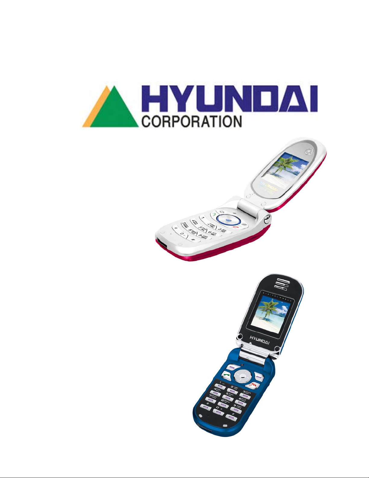
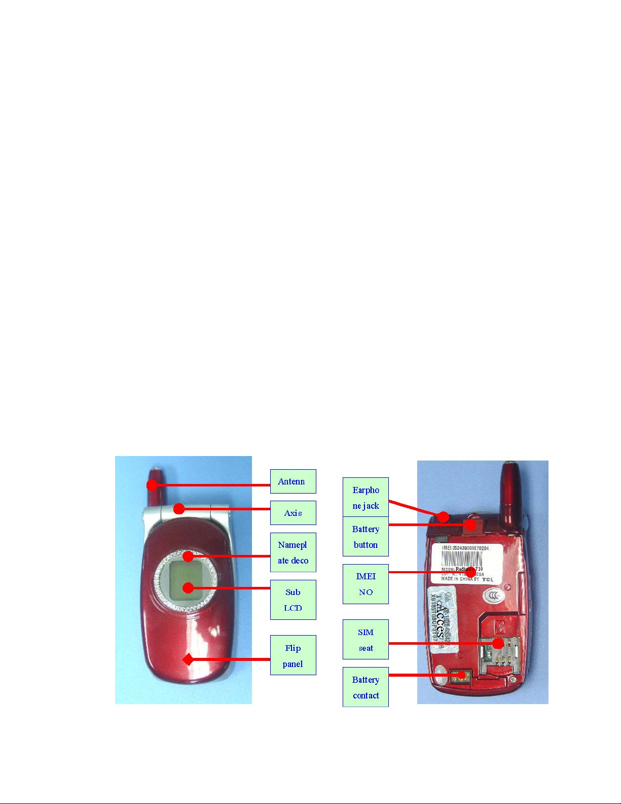
1. The cell phone has a diamond nameplate on main panel and double single-color LCDs (65000
shades) as shown in Fig. 1 and Fig. 2:
Fig. 1 Fig. 2
3
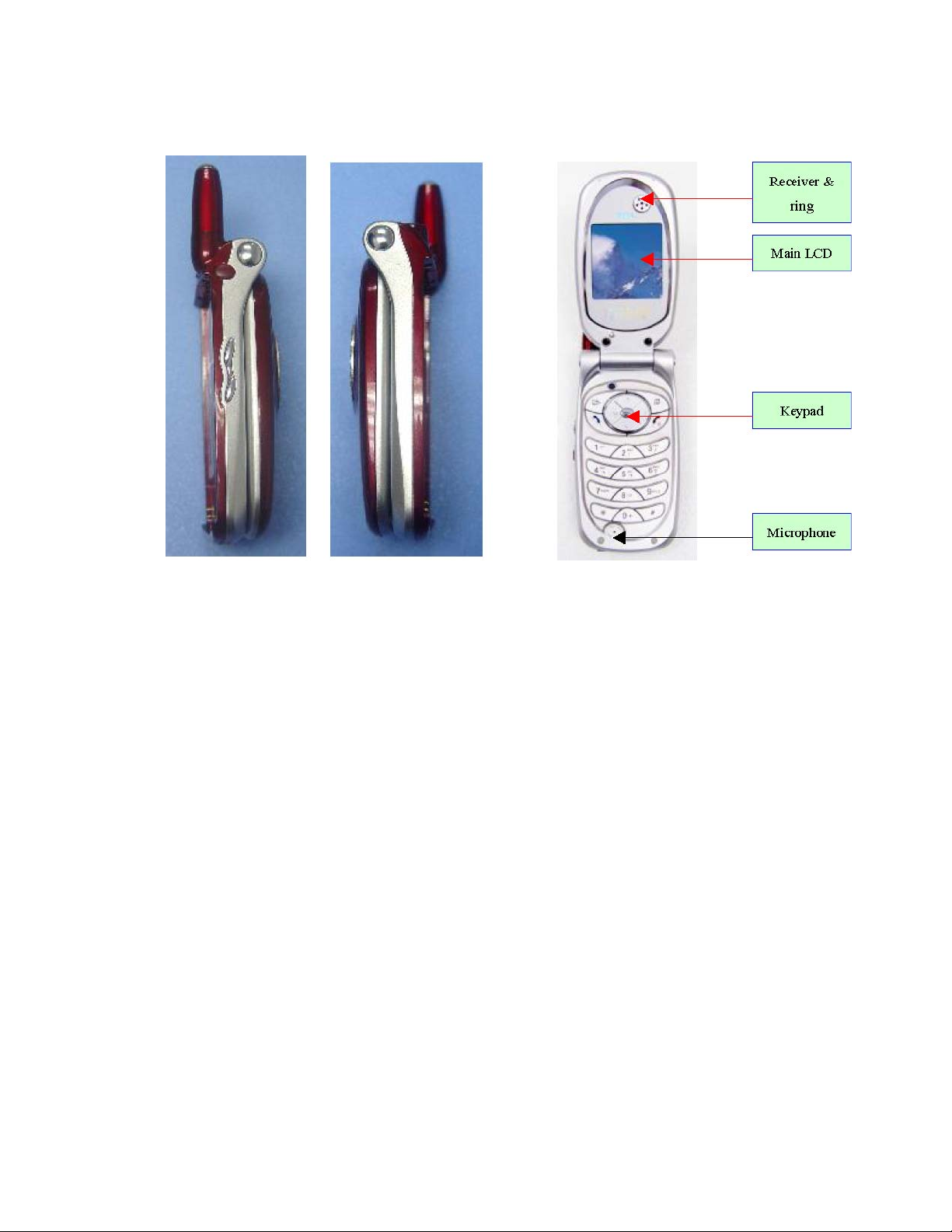
2. The side view is shown in Fig. 3 and Fig. 4. There are two side buttons and one RF port. The side
keys are usually used to regulate volume and to switch time mode.
Fig. 3 Fig. 4
4
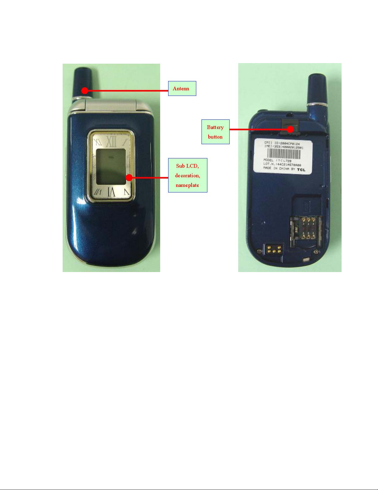
II. Model 728 Outer View
5
Chapter 2 Dismantling and Assembly
I.
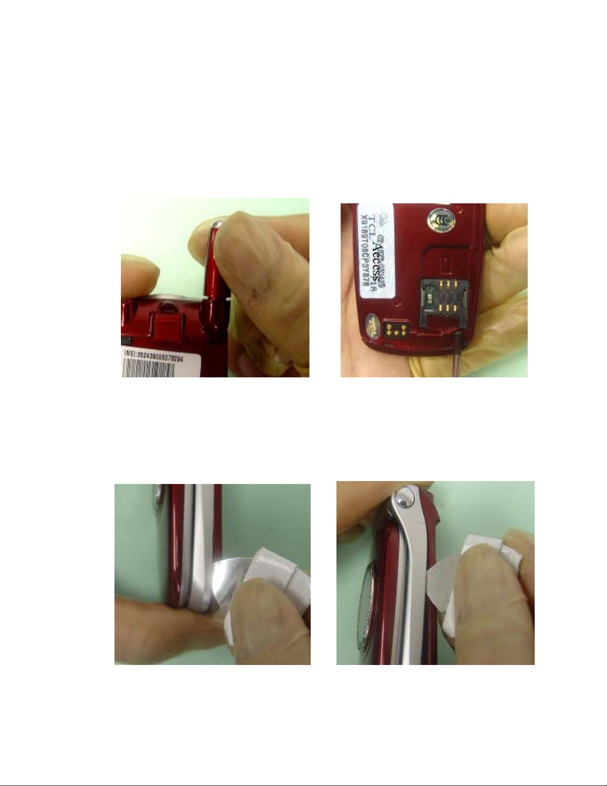
1. Unscrew and remove antenna, and remove screws with a Philips driver (two screws on main back
case) as shown in Fig. 5 and Fig.6:
Fig. 5 Fig. 6
2. Insert a small blade between the main panel case and main back case, and move it slowly up and
down to unlock the buckle between the two. Mind not to damage the cases (Fig. 7 and Fig. 8):
Fig. 7 Fig. 8
6
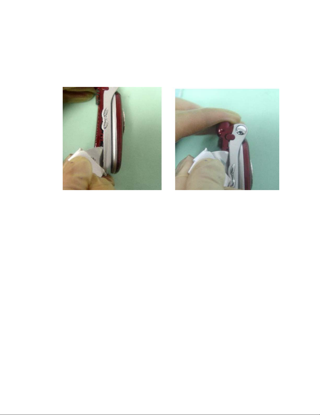
3. Unlock the two buckles on the other side and push the cases with force towards
different directions. Mind not to scratch cases (Fig. 9 and Fig. 10):
Fig. 9 Fig. 10
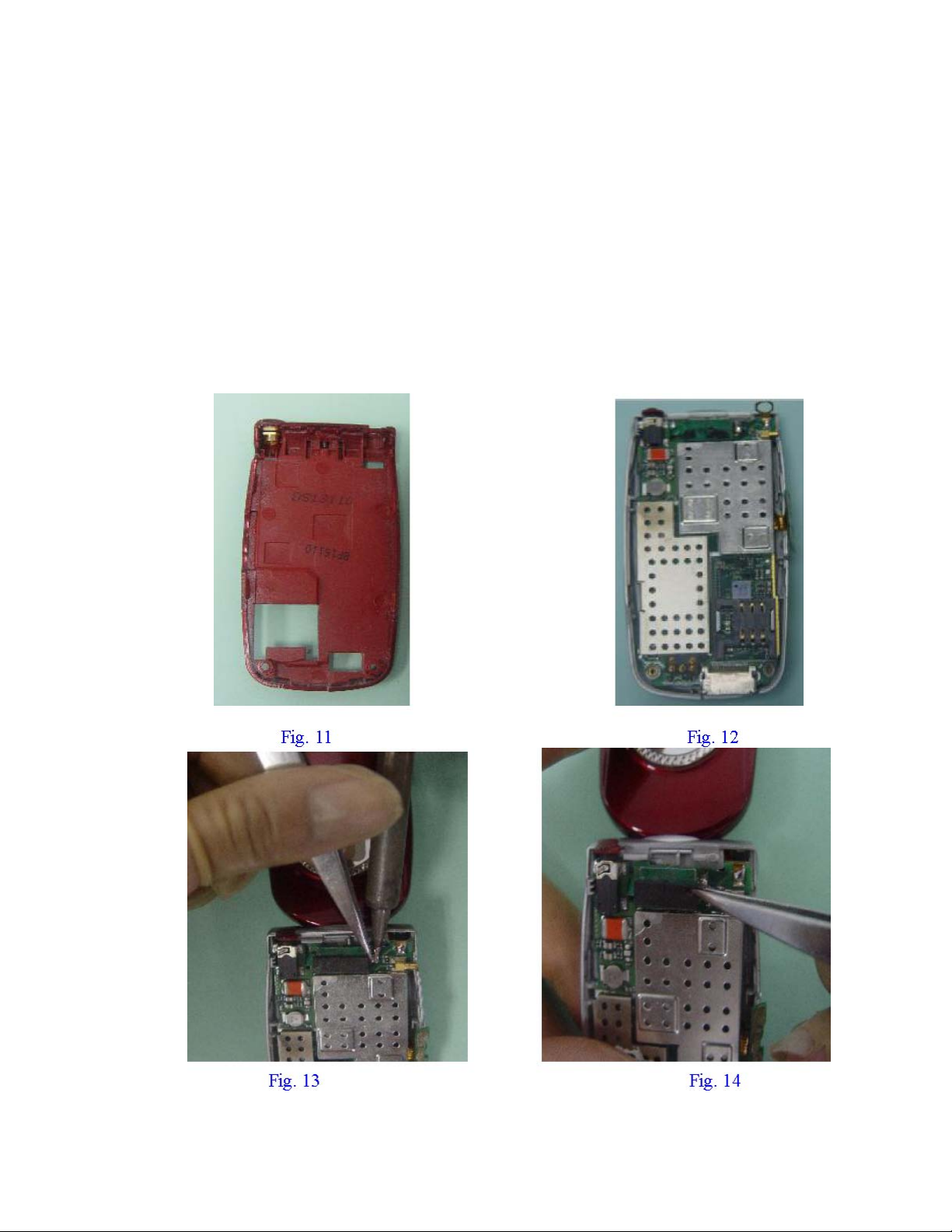
4. Mind not to damage the antenna contact, earphone cap and the two buckles at the
top of cases when splitting them. The inside view is shown in Fig. 11 and Fig. 12:
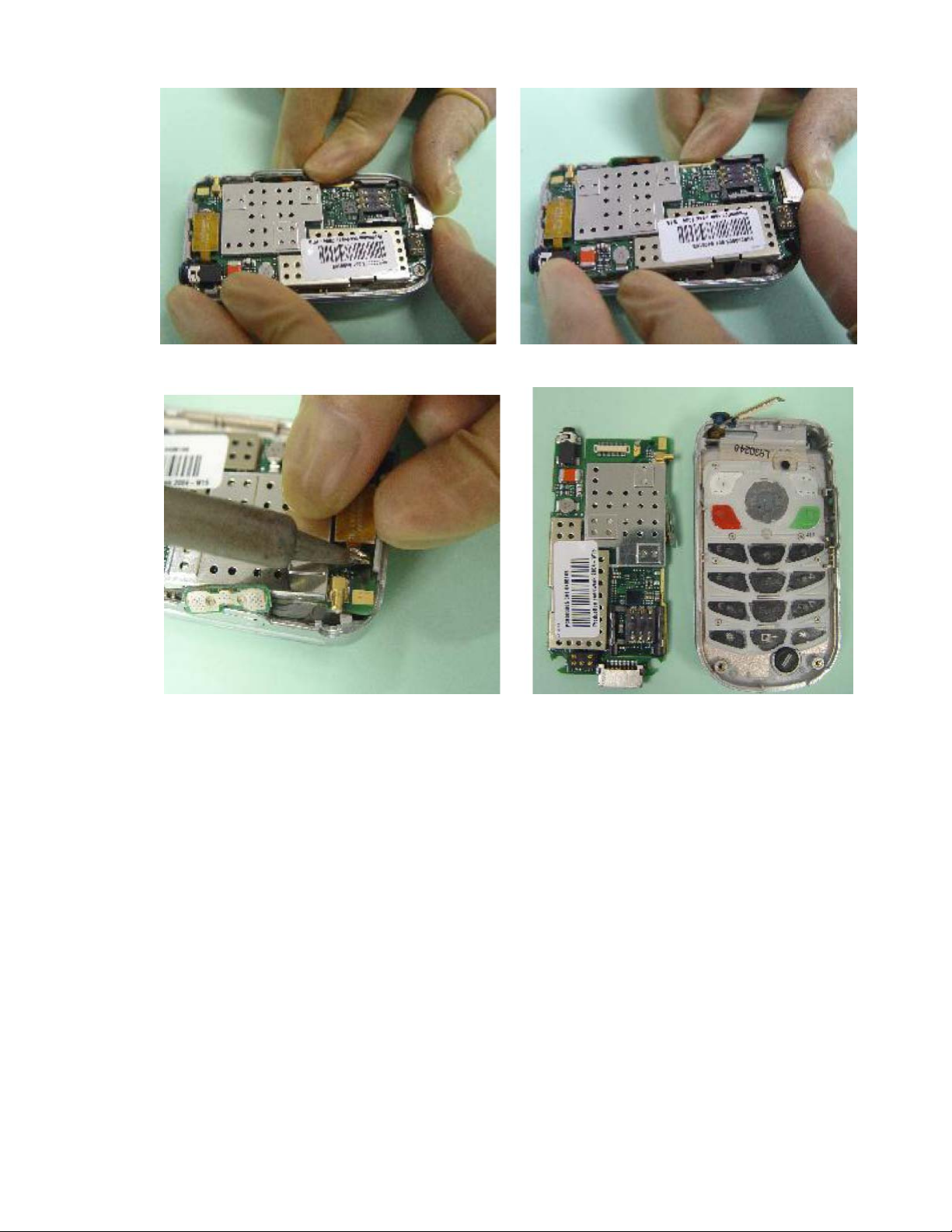
5. Use an iron to remove FPC line solder points and disconnect FPC from the
mainboard with a pair of forceps. Mind not to damage the cases or break the FPC
line (Fig. 13 and Fig. 14):
6. To separate flip component from main panel, hold the main panel in hand and use a
hook to push flip component by the axis. When the axis leaves main panel, press
the axis with hook and push flip component out (Fig. 15 and Fig. 16):
7
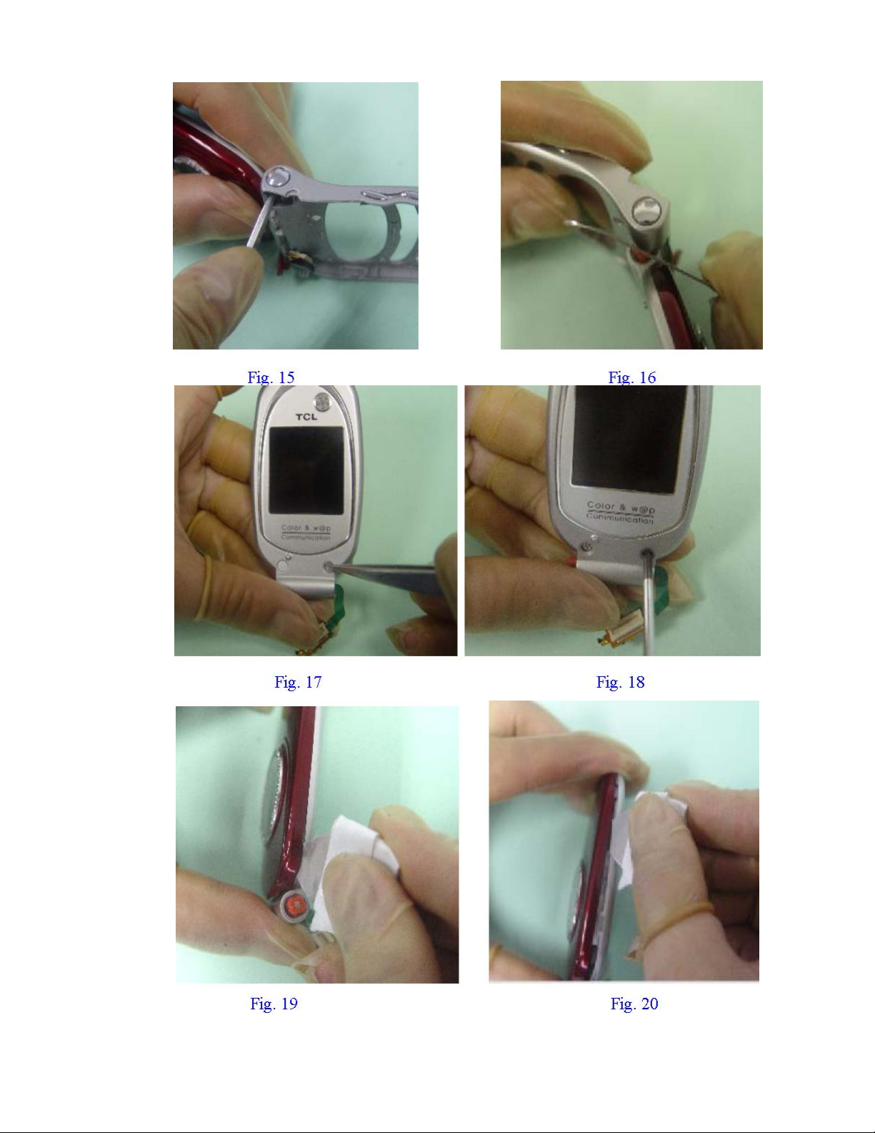
7. The flip component has two screws. Hold flip component in hand, remove screw
cap with a pair of forceps and remove screws with a screwdriver (Fig. 17 and Fig. 18):
8. Hold flip component in hand, insert a small blade into flip component and move it
slowly to the second buckle (Fig. 19 and Fig. 20):
8
1. 9. Separate flip panel from flip back and attach a transparent film on sub LCD. Do not touch
9
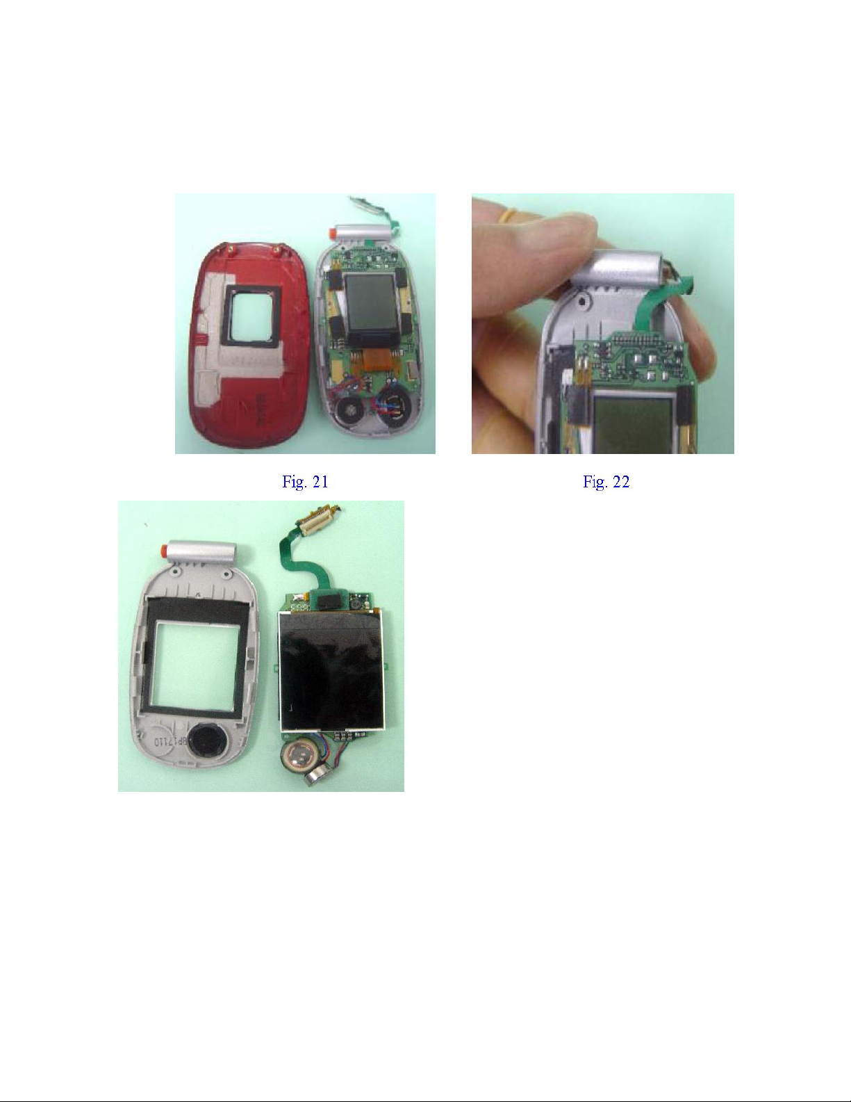
LCD surface with fingers. Remove LCD component along the bend of the FPC line. Do not damage
FPC line (Fig. 21 and Fig. 22):
2. 10. Attach a transparent film on main LCD of LCD component. Do not touch LCD surface
with fingers. LCD surface scratch should be absolutely avoided. Otherwise, the LCD might be
destructed (Fig. 23):
Fig. 23
10
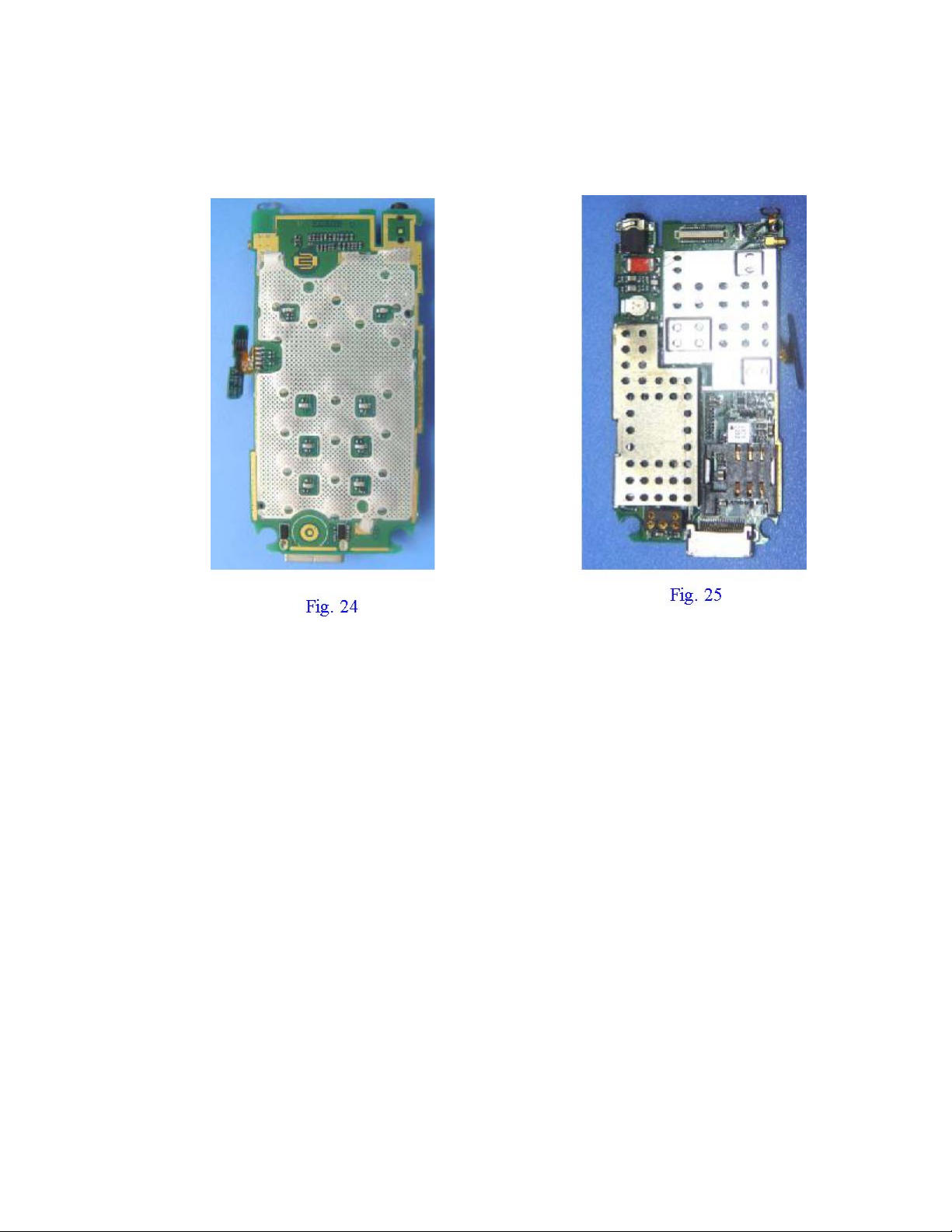
11. The front and back view of the mainboard is given in Fig. 24 and Fig. 25. Do not spoil such
peripheral devices as side buttons, button springs and shield cover:
12. The assembly of cell phone is contrary to the dismantling. During the assembly, do not remove
LCD film, and buckles and elements soldering should be installed in right
position to avoid element damage. Special attention should be paid to the
prevention of dirt. LCD surface should be cleaned and cell phone tested after
assembly.
11
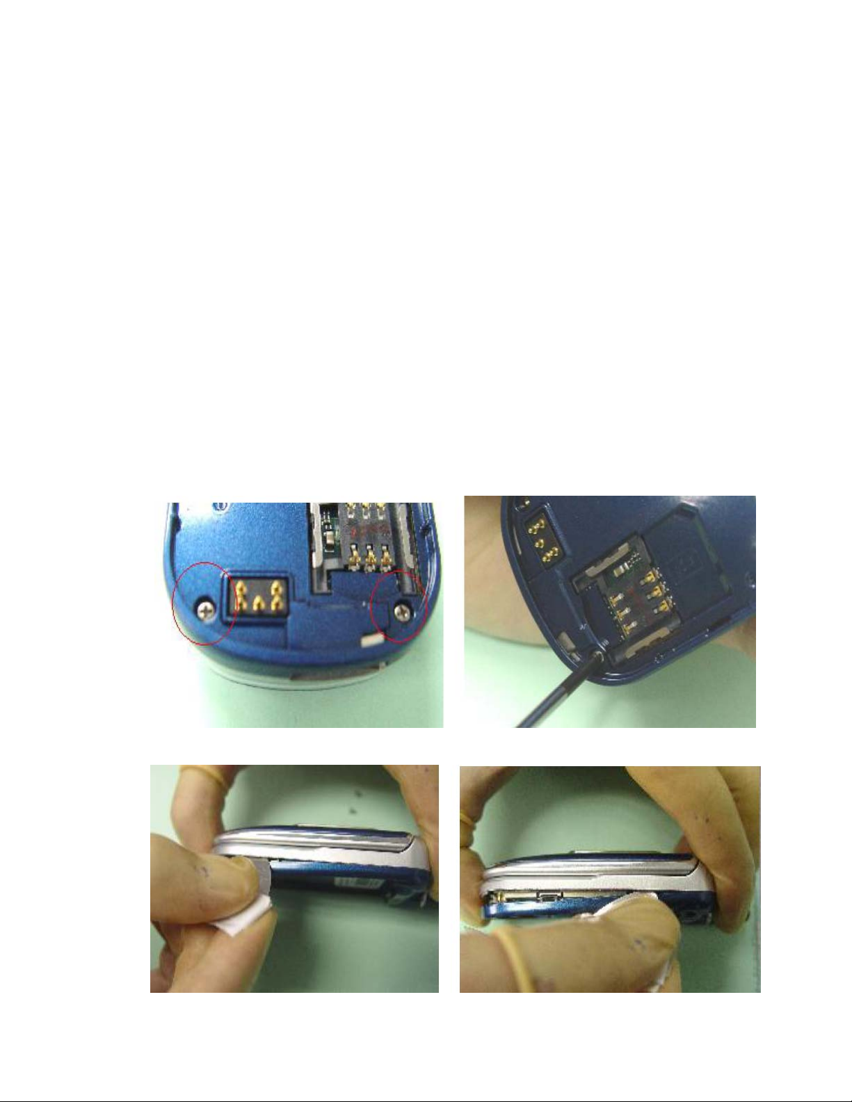
II. Models 728 and 738 Dismantling Flow
1. 1. The main back has two screws. Hold cell phone in hand and remove screws with a Philips driver
as shown below:
2. 2. As shown in Fig. 5, hold cell phone in hand, insert a small blade in cell phone from lower
end, and
Otherwise, it will be unable to reassemble.
3. 3. Hold cell phone by the other end, insert small blade into bottom end on the other side and
move it slowly upward to the first buckle (this only one buckle) (Fig. 7).
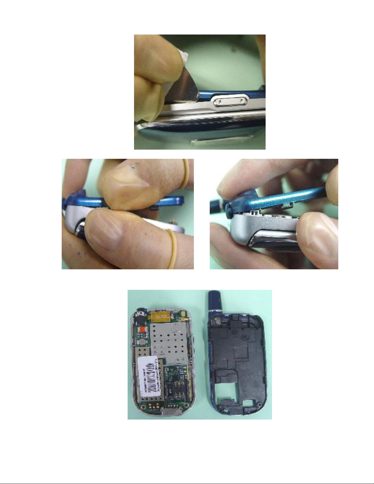
4. 4. Hold flip component and main panel in one hand, and main back in the other. Turn main
back left and right slightly and pull upward at the same time. Make it tender to avoid damage to the
buckle at the top of main back.
5. 5. Separate main panel from main back as shown below:
6. 6. As shown in figure below. Hold sides of main panel in both hands, press mainboard
bottom with two thumbs and push upward and remove mainboard from main panel case.
7. 7. Hold FPC line and use a iron to remove it and then separate mainboard from flip
component.
8. 8. When separating flip component from main panel, hold main panel in hand, press axis
with a hook and push flip component slightly. When axis leaves main panel, press it with hook and
push out flip component. Mind not to scratch the case or break the FPC line.
move it upward till the second buckle. Mind not to scratch cases or damage case buckle.
12
13
14
 Loading...