HYNIX HMS91C8032, HMS97C8032 Datasheet

HYNIX SEMICONDUCTOR INC.
8-BIT SINGLE-CHIP MICROCONTROLLERS
HMS91C8032
HMS97C8032
User’s Manual
(Ver. 1.02)

REVISION HISTORY
VERSION 1.01 (JUL., 2001) sticker
Add the interrupt control block and changed the P2.0 ~ P2.3 pins schematic block.
VERSION 1.02 (NOV., 2001) sticker
Changed Power-On Reset Circuit.
Version 1.02
Published by
MCU Team
2001 Hynix Semiconductor Inc. All right reserved.
Additional in for matio n of thi s ma nua l may be se rv ed b y H ynix Sem ico ndu ctor o ff ice s in Kor ea o r Dis tri butor s and Repr es entativ es liste d
at address directory.
Hynix Semiconductor reserves the right to mak e chang es to any info rma tion he re in at any time withou t no tice.
The information, diagrams and othe r data in this m anua l are c orrect a nd reli able; h oweve r, Hyni x Se micondu ctor is in no way responsible
for any violations of patents or other rights of the third party generated by the us e of this manual.

Table of Contents
HMS91C8032/97C8032
1. OVERVIEW............................................1
Description .........................................................1
Ordering Information
Features ............................... ..............................2
Pin Description .............. ....... ...... ....... ...... ....... .... 3
Pin Diagram ...................................... ...... ....... .... 5
2. MEMORY ORGANIZATION...................6
Program Memory .............................. ...... ....... .... 6
Data Memory .....................................................6
Special Function Register ..................................7
3. INSTRUCTION SET...............................8
Program Status Word ... ....... ...... ....... .................8
Addressing Modes .............................................8
Arithmetic Instructions ........................................9
Logical Instructions ..........................................10
Data Transfers .................................................11
Lookup Tables .................................................12
Boolean Instructions ........................................13
Relative Offset .................................................13
Jump Instructions .............................................13
CPU Timing ......................................................15
Machine Cycles ................................................16
4. HARDWARE DESCRIPTION...............17
Clock Generation Block ...................................18
Special Function Registers ..............................19
Timer/Counters (Timer0, Timer1 and Timer2) .43
Timer/Counters (Timer3 and Timer4) ..............47
Standard Serial Interface (UART) ....................49
Standard Serial Interface (SIO 1, SIO 2) .........57
Port Structure and Operation .......................... 66
Watch Dog Timer ............................................ 68
Buzzer ........................ ..................................... 70
IF Counter ........... ....... ...... ....... ........................ 71
PLL ...................... ....................................... ..... 76
ADC ............................ ............. ............. ........... 83
Interrupts .......................... ............................... 85
Reset .......................... ..................................... 89
Power-On Reset .............................................. 89
Power-Saving Modes of Operation ................. 90
The On-Chip Oscillators .................................. 91
5. ELECTRICAL CHARACTERISTICS....9 3
Operating Conditions ...................................... 93
AC Characteristics .......................................... 93
DC Characteristics .......................................... 97
6. INSTRUCTION DEFINITIONS.............99
Instruction Set Summary ................................. 99
Instruction Definitions .................................... 102
7. EPROM CHARACTERISTICS...........145
Reading the Signature Bytes: ....................... 145
Modified Quick-Pulse Programming .............. 145
Program Verification ...................................... 146
8. OTP PROGRAMMING.......................150
HMS97C8032 OTP Programm in g . ....... ......... 150
Device Configuration Data ........................... 150
9. DEVELOPMENT TOOLS...................152
10. PACKAGE DIMENSION..................153
HMS97C8032/91C8032 (80 pin package) .... 153
NOV., 2001 Ver 1.02
HMS91C8032/97C8032
HMS91C8032
HMS97C8032
1. OVERVIEW
1.1 Description
The HMS91C8032 and the HMS97 C8032 are a me mber of the HMS9XC80 32 series. T his devices a re the Dig ital Tuning System(DTS)
with PLL. It has extended Intel 8051 core, 32Kbytes one-time programmable(OTP) ROM. Because this device can be programmed by user,
it is suited for applications such as the small-scale production of many different products and rapid development and time-to-market of
new products.
• Extended 8051 core (7.2MHz / 32.768KHz)
• 1K-Byte Data RAM / 32K-Byte Program ROM
• 130 MHz Digital PLL block
• IFC (Intermediate Frequency Counter)
• 8-channel 8-bit ADC
• Five 16-bit Timers/Counters
• Two 3-wire SIO & One UART
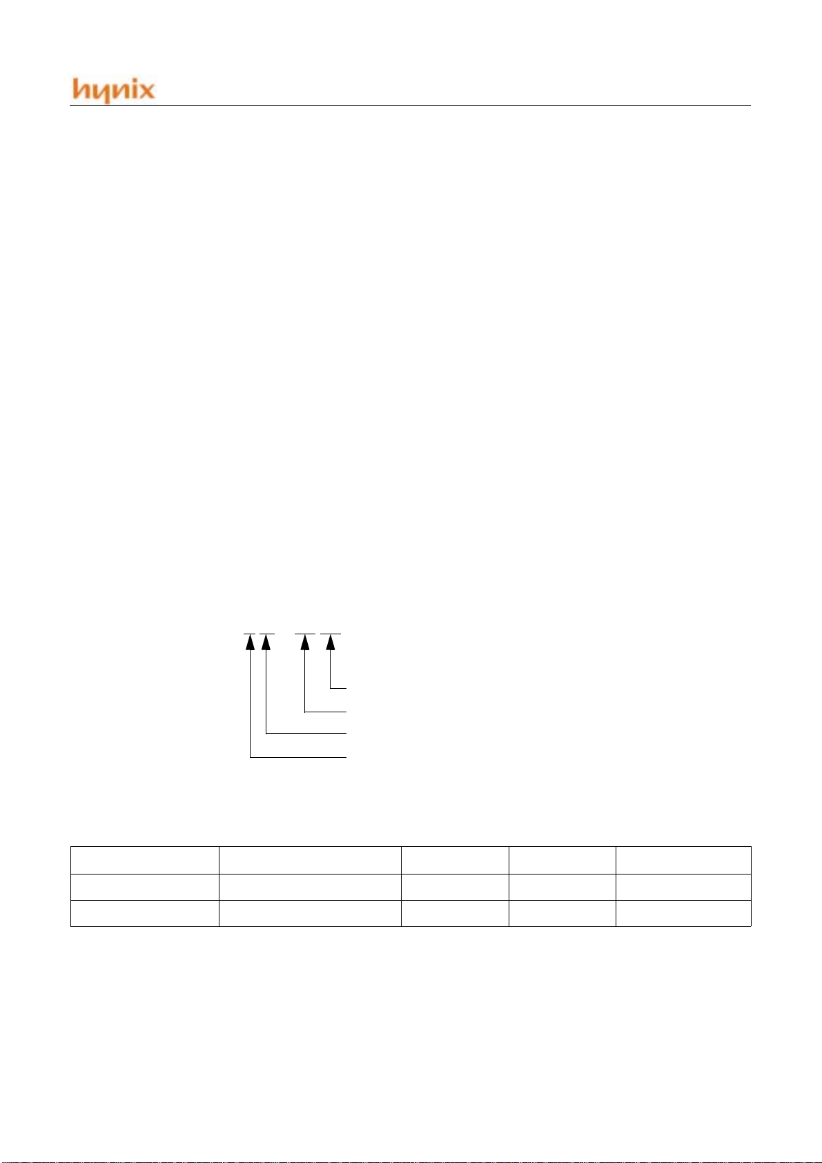
HMS9XC8032
32K ROM
Automotive application
7 : O TP , 1 : MAS K
Extended 8051 core family MCU
• 18 Interrupts Sources( 7 External Interrupts / 5
Timer Interrupts / 3 Serial Port Interrupts / WDT
Interrupt / IF Counter Interrupt / ADC Interrupt ),
Two Priority Levels
• Two Power Saving Mode (Idle Mode and Power
Down Modes)
•5V
10% Power supply
±±±±
• 80-MQFP Package
1.2 Ordering Information
Device na me ROM Size (bytes) RAM size Package
HMS91C8032 32K 1024 bytes 80MQFP Mask ROM version
HMS97C8032 32K bytes OTP 1024 bytes 80MQFP OTP ROM version
NOV., 2001 Ver 1.02 1

HMS91C8032/97C8032
1.3 Features
Item Features
ROM 32K x 8-bit
RAM 1K x 8-bit
Instruction Cycle
Instruction Set MCS-51 Micro-controller Compatible Instruction Set
I/O Port CMOS I/O : 62 pins (including 4-open drain ports)
A/D Converter 8-bit resolution x 8-channels
With variable instruction execution time function
1.66µs / 3.33µs / 26.6µs (with main system clock : 7.2MHz)
366.2µs (with sub-system clock : 32.768KHz)
Serial Interface
Timer/Counter
Buzzer(Beep) Output 1.2KHz (fx/6000), 2.4KHz (fx/3000), 4.5KHz (fx/1600), 8.0KHz (fx/900)
Interrupt Source 7 External, 11 Internal Sources
PLL
Frequency
Synthesizer
Frequency Counter
Standby Function
Division Mode
Reference
Frequency
Charge Pump Error out : EO pin
Phase Detector Unlock detectable by program
Reset
3-wire serial I/O mode : 2 channels
Full duplex UART : 1 channel
Five 16-bit timers/event counters
Dedicated Watchdog timer
Direct divis ion mode (VCOL pin)
Pulse swallow mode (VCOH and VCOL pins)
13 types selected by program
1, 1.25, 2.5, 3, 5, 6.25, 9, 10, 12.5, 18, 20, 25, 50KHz
Frequency Measur em en t
AMIFC pin : for 450KHz count
FMIFC pin : for 10.7MHz count
Idle mode
Power-down mode
Reset by RESET pin
Reset by Vdet circuit
Vdet circuit: Detection of less than 2.7V (Normal operation mode)
Power Supply Voltage
System Clock
Package 80 pin plastic MQFP
VDD = 4.5V to 5.5V (with PLL operating)
VDD > 1.8V (Data retention mode)
Main system clock : 7.2MHz
Sub-system clock : 32.768KHz
2 NOV., 2001 Ver 1.02

1.4 Pin Description
HMS91C8032/97C8032
Pin
Names
1
2
3
4
5
6
7
8
9
10
11
12
13
14
15
16
17
18
19
20
21
22
23
24
Port
Names
P0.0
P0.1
P0.2
P0.3
P0.4
P0.5
P0.6
P0.7
P1.0
P1.1
P1.2
P1.3
P1.4
P1.5
P1.6
P1.7
P2.0
P2.1
P2.2
P2.3
P2.4
P2.5
P2.6
P2.7
Alternative
s
N-ch
N-ch
N-ch
N-ch
Functions
8-bit general purpose bidirectional
Pin
Input and output mode selected by
8-bit Port Mode Register.
In Input mode, pin can use on-chip
pullup resister by software.
8-bit general purpose bidirectional
Pin
Input and output mode selected by
8-bit Port Mode Register.
In Input mode, pin can use on-chip
pullup resister by software.
8-bit general purpose bidirectional
Pin
Input and output mode selected by
8-bit Port Mode Register.
In Input mode, P2.4~P2.7pin can
use on-chip pullup resister by software. P2.0~P2.3pin have no pullup
Rese
t
LED drive ability. Input
Input
N-channel open drain (P2.0 P2.3)
N-channel open drain voltage :
Max. 6V
Input
25
26
27
28
29
30
31
41
71
32
50
74
33
34
35
36
37
38
39
40
P3.0
P3.1
P3.2
P3.3
P3.4
P3.5
VSS1
VSS2
VSS3
VDD!
VDD2
VDD3
P4.0
P4.1
P4.2
P4.3
P4.4
P4.5
P4.6
P4.7
T0
T1
T2
T3
T4
T2EX
INT0
INT1
INT2
INT3
INT4
INT5
INT6
BEEP
6-bit general purpose bidirectional
Pin
Input and Output mode selected by
8-bit Port Mode Register.
Ground -
DC
Supply Voltage is 5V +/- 10%.
In Power down mode, RAM data guaranteed until 1.8V
All VDD pin is connected in system.
VDD1 : I/O VDD, VDD2 : core VDD, VDD3 : analog VDD
8-bit general purpose bidirectional
Pin
Input and output mode selected by
8-bit Port Mode Register.
In Input mode, pin can use on-chip
pullup resister by software.
P3.0 - P3.5 pin can use Timer
input pin
P4.0 - P4.6 is External Interrupt
input pin.
level/falling detect : 2 pin
level/edge detect : 5 pin
P4.7 is beep clock putput.
Input
Input
-
NOV., 2001 Ver 1.02 3

HMS91C8032/97C8032
41
42
43
44
45
46
47
48
49
50
51
52
53
54
55
56
57 TstEn Ground
60 Avref+
61
62
63
64
65
66
67
68
P5.0
P5.1
P5.2
P5.3
P5.4
P5.5
P5.6
P5.7
P6.0
P6.1
P6.2
P6.3
P6.4
P6.5
P6.6
P6.7
P7.0
P7.1
P7.2
P7.3
P7.4
P7.5
P7.6
P7.7
TxD
RxD
SCK1
SO1
SI1
SCK2
SO2
SI2
ANI0
ANI1
ANI2
ANI3
ANI4
ANI5
ANI6
ANI7
8-bit general purpose bidirectional
Pin
Input and output mode selected by
8-bit Port Mode Register.
In Input mode, pin can use on-chip
pullup resister by software.
8-bit general purpose bidirectional
Pin
Input and Output mode selected by
8-bit Port Mode Register.
In Input mode, pin can use on-chip
pullup resister by software.
This pin is oniy ground.
Chip test pin
A/D converter reference voltage input pin
In AD converter, signal from ANI0 ~ ANI7 change to digital signal by reference between AVref+ and VSS.
8-bit general purpose bidirectional
Pin
Input and output mode selected by
8-bit Port Mode Register.
In Input mode, pin can use on-chip
pullup resister by software.
TxD, RxD : Asynchronous serial
data pin
SI1, SI2, SO1, SO2 : Synchronous
serial data pin
SCK1, SCK2 : Clock pin for Synchronous serial data
A/D converter 8-channel analog
input pin
If pin is not used by A/D converter
input, can use to general-purpose
bidirectional pin.
Input voltage in ANI0 - ANI7 is
between Avref+ and VSS.
Input
Input
GND
Input
69 AMIFC AM IF input pin
70 FMIFC FM IF input pin
72 VCOH FM band VCO frequency input pin
73 VCOL AM band VCO frequency input pin
Error output pin in PLL part (charge pump output)
75 EO
76 RESET Chip reset pin. Reset is active high.
77 Xin Crystal oscillator input pin for main system clock
78 Xout Main system clock output pin
79 Xtin Crystal oscillator input pin for Sub system clock
80 Xtout Sub system clock output pin
If tuning freq. = VCO freq., EO pin is floating.
If tuning freq. > VCO freq., EO pin is high.
If tuning freq. = VCO freq., EO pin is low.
4 NOV., 2001 Ver 1.02

1.5 Pin Diagram
P0.0
P0.1
P0.2
P0.3
P0.4
P0.5
P0.6
P0.7
P1.0
P1.1
P1.2
P1.3
P1.4
P1.5
P1.6
P1.7
P2.0
P2.1
P2.2
P2.3
P2.4
P2.5
P2.6
P2.7
10
11
12
13
14
15
16
17
18
19
20
21
22
23
24
1
2
3
4
5
6
7
8
9
XTout
XTin
79
80
Open Drain &
}
No Pull-up
25
26
Xout
Xin
78
RESETEOVDD3
76
77
75
74
VCOL
73
VCOH
72
HMS91C8032
HMS97C8032
P2.0~P2.3)
27
28
29
30
31
32
33
VSS3
71
34
FMIFC
70
35
AMIFC
69
36
P7.7/ANI7
68
37
P7.6/ANI6
67
38
P7.5/ANI5
66
39
HMS91C8032/97C8032
P7.4/ANI4
65
64
P7.3/ANI3
63
P7.2/ANI2
62
P7.1/ANI1
61
P7.0/ANI0
60
Avref+
59
VDD2
58
VSS2
57
TSTEN
(Only Ground)
56
P6.7
55
P6.6
54
P6.5
53
P6.4
52
P6.3
51
P6.2
50
P6.1
49
P6.0
48
P5.7/SI0
47
P5.6/SO0
46
P5.5/SCK0
45
P5.4/SI1
44
P5.3/SO1
43
P5.2/SCK1
42
P5.1/RxD
41
P5.0/TxD
40
VSS1
P3.0/T0
P3.1/T1
P3.2/T2
P3.3/T3
P3.4/T4
P3.5/T2EX
VDD1
P4.0/INT0
P4.1/INT1
P4.2/INT2
P4.3/INT3
P4.4/INT4
P4.5/INT5
P4.6/INT6
P4.7/BEEP
Figure 1-1 HMS9XC8032 Pin Diagram
NOV., 2001 Ver 1.02 5
HMS91C8032/97C8032
2. MEMORY ORGANIZATION
All HMS91C8032 de vices hav e separ ate add ress sp ace s for p rogram and data memory. The logical separation of program and
data memory allows the data memory to be accessed by 8-bit addresses, which can be quickly stored and manipulated by an 8-bit
CPU.
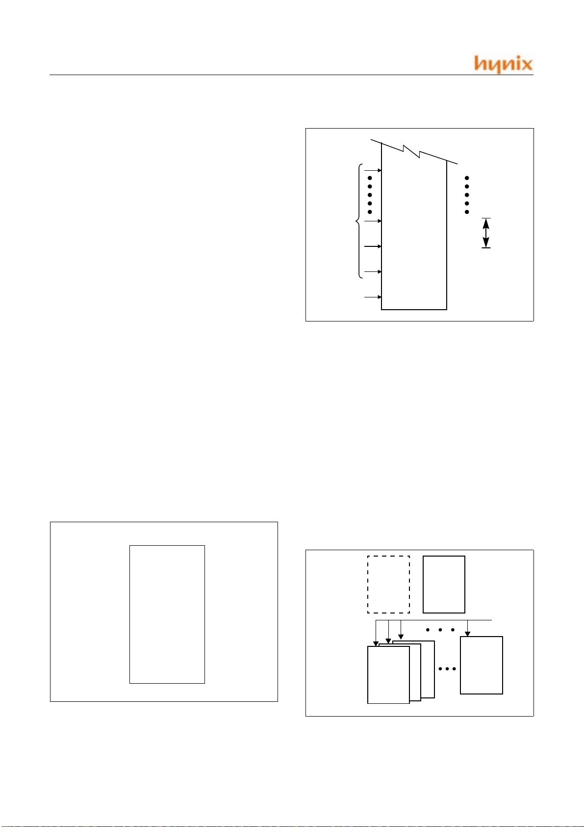
Program memory (ROM) can only be read, not written to. There
can be up to 32K bytes of program memory. In the
HMS9XC8032 devices, the Program Memory is provided
on-chip.
Data Memory (RAM) occupies a separate address space from
Program Memory. In the HMS9XC8032, the data memory is
on-chip.
Interrupt
Location
008BH
0013H
8 Bytes
000BH
2.1 Program Memory
Figure 2-1 shows a map of the lowe r pa r t o f the Pr o gr a m Me mo ry. After reset, the CPU begins executi on from lo cati on 0000 H.
As shown in Figur e 2-2, each in terrupt is assigne d a fixe d location in Program Memory. The interrupt causes the CPU to jump
to that location, wher e it commences ex ecution of the se rvice routine. External Interrupt 0, for example , is assigned to location
0003H. If External Interrupt 0 is going to be used, its service routine must begin at location 0003H. If the interrupt is not going to
be used, its service location is available as general purpose Program Memory.
The interrupt service locations are spaced at 8-byte intervals :
0003H for External Interrupt 0, 000BH for Timer 0, 0013H for
External Interrupt 1, 001BH for Timer 1 and etc. If an interrupt
service routine is short enou gh (as is often the case in control applications), it can reside entirely within that 8-byte interval.
Longer service routines can use a jump instruction to skip over
subsequent interrupt locations, if other interrupts are in use.
Program Memory addresses are always 16bits wide, even though
the actual amount of Program Memory used may be less than 32K
bytes.
7FFFH
0003H
Reset
0000H
Figure 2-2 Interrupt Location of Program Memory
2.2 Data Memory
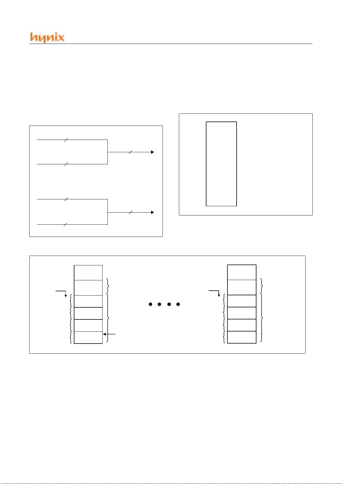
Figure 2-3, Fi gure 2-6 and Fig ure 2-6 shows the Memory spaces
available to the HMS9XC8032 use r. HMS9XC8032 can address
up to 1kbytes of data memory . 10bits address is config ured as follows.
10bits address for READ memory operation = 2bits of RDPG +
8bits of implied address in instruction
10bits address for WRITE memory operation = 2bits of WRPG +
8bits of implied address in instruction
(Where, 0 =< RDPG, WRPG =< 6)
(CAUTIONS: A valid value which can be stored in RD PG and
WRPG must be from 0 to 6. 7 is reserved for indirect addressable
memory region.( upper 128byt es region) A progr ammer who set
RDPG/WRPG to 7 or greater than 7 will get the invalid memory
operation results. )
7FH
Accessible
by Direct
Addressin g
Accessible
by Direct
Addressin g
RDPG
WRPG
32Kbyte
0000H
Upper
128
00H
7FH
Lower
128
00H
Accessible
by Indirect
Addressing
Only
Accessible
by Direct
Addressing
Figure 2-1 Program Mamory
Figure 2-3 Data Memory Structure
6 NOV., 2001 Ver 1.02
HMS91C8032/97C8032
Data memory consists of 7 pages, and each page can store
128bytes. According to the value of RDPG(FCH) and WRPG(FDH), HMS9XC8032 selects working memory page. Figure
2-4 shows the generation method of in ternal data memory address. For example, to read from data memory, HMS9XC8032
references the content of RDPG, generates 10bits address and ac-
RDPG [2 : 0]
3
Implied address of instruction
7
WRPG [2 : 0]
3
Implied address of instruction
7
RAM Read Address
10
RAM Write Address
10
cesses the corresponding data. The following two cases are
equivalent.
MOV 00H, A 1)
MOV R0, A 2)
FFH
No Bit-Addressable Spaces
80H
Figure 2-5 Upper 128bytes of Internal RAM
Figure 2-4 Data Memory Address Generation Method
7FH
Bank
Select
Bits
in PSW
2FH
20H
11
18H
10
10H
01
08H
00
0
1FH
17H
0FH
07H
Bit-Addressable
Space
(Bit Addresses 0-7F)
4 Banks of
8 Registers
R0-R7
Reset Value of
Stack Pointer
Page 0
Figure 2-6 Page0 ~ Page6 of Internal RAM
2.3 Special Function Register
Unlike Intel 805X series, HMS9XC8032 has two SFR pages. If
the content of SFRPG (address:FFH) is clear to 00H(01H),
HMS9XC8032 assumes working SFR page to SFR page 0(1).
Byte-addressing only registers in SFR pages have the same address in each SFR pages, but bit addressing registers in SFR page
7FH
Bank
Select
Bits
in PSW
2FH
20H
11
18H
10
10H
01
08H
00
0
1FH
17H
0FH
07H
Bit-Addressable
Space
(Bit Addresses 0-7F)
4 Banks of
8 Registers
R0-R7
Reset Value of
Stack Pointer
Page 6
0 and SFR page 1 are different except ACC, B and PSW.
The Port Data registers are located to SFR page1, and the Periph-
eral Control registers to SFR page0. Refer to "4.2 Special Function Registers" on page 19.
NOV., 2001 Ver 1.02 7
HMS91C8032/97C8032
HMS91C8032/HMS97C8032 Description
3. INSTRUCTION SET
The HMS9XC8032 instruction set is optimized for 8-bit control applications. It provides a variety of fast addressing modes for accessing
the internal RAM to facilitate byte opera tions on small data structure s. The instru ction set p rovid es extensi ve suppo rt for one - bit variables
as a separate data type, allowing direc t bit manipulation in control and logic syst ems that require Bool ean processing.
3.1 Program Status Word
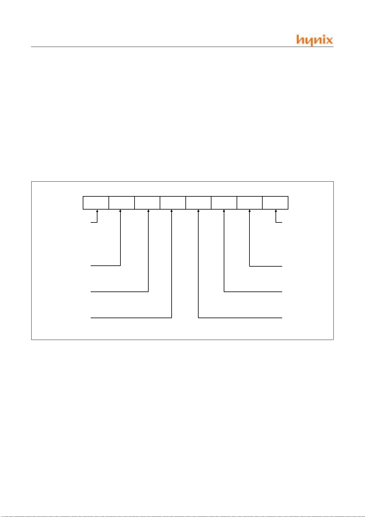
The Program Status Word (PSW) contains several status bits that
reflect the current stat e of the CPU. T he PSW, sho wn in Figu re
3-1, resides in the SFR space. It contains the Carry bit, the Auxiliary Carry (for BCD operations), the two register bank select
bits, the Overflow flag, a Parity bit, and two user-definable status
flags.
The Carry bit, other than serving the functions of a Carry bit in
arithmetic o perations, also serves as the “A ccumulator” for a
number of Boolean operations.
AC -CY F0 RS0 OV P
Carry flag receives carry out
from bit 7 of ALU operands
Auxiliary carry flag receives
carry out from bit 3
of addition operands
General purpose status flag
Register bank select bit 1
PSW 7
PSW 6
PSW 5
PSW 4
Figure 3-1 PSW (Program Status Word) Register in HMS9XC8032 Devices
RS0 and RS1 are used to select one of the four register banks.
Each register bank composed of eight registers.(R0 to R7) The
selection of a register bank is made at execution time.
The parity bit reflects the nu mbe r o f 1s in th e Accu m ulato r: P= 1
if the Accumulator contains an odd number of 1s, and P = 0 if the
Accumulator contains an even number of 1s. Thus the number of
1s in the Accumulator plus P is always eve n. Two bits in the PS W
are uncommitted and may be used as gen eral-purpose status
flags.
RS1
PSW 0
Parity of accumulator
set by hardware to 1 if it
contains an odd number
of 1s; otherwise it is
reset to 0
PSW 1
User-definable flag
PSW 2
Overflow flag set by
arithmetic operation
PSW 3
Register bank select bit 0
Direct Addressing
In direct addressing the op erand is specif ied by an 8-bit address
field in the instruction. Only interna l Data RAM an d SFRs can be
directly addressed.
Indirect Addressing
In indirect addressing the instruction specifies a register which
contains the address of the operand. Both internal and external
RAM can be indirectly addressed.
3.2 Addressing Modes
The addressing modes in the HMS9XC8032 instruction set are as
follows:
The address register for 8-bit addresses can be R0 or R1 of the selected bank, or the Stack Pointer. The address register for 16-bit
addresses can only be the 16-bit "data po inter" register, DPTR.
8 NOV., 2001 Ver 1.02
HMS91C8032/97C8032
Register Instructions
The register banks, containing registers R0 through R7, can be
accessed by certain instructions which carry a 3-bit register specification within the opcode o f the instruction. Inst ructions that access the registers this way are code efficient, since this mode
eliminates an address byte. When the in struction is executed , one
of the eight registers in the selected bank is accessed. One of four
banks is selected at execution time by the two bank sel ect bits in
the PSW.
Register-Specific Instructions
Some instructions are specific to a certain register. For example,
some instructions always operate on the Accumulator, or Data
Pointer, etc., so no address byte is needed to point to it. The opcode itself does that. Instructions that refer to the Accumulator as
A assemble as accumulator specific opcodes.
Immediate Constants
The value of a constant can follow the opcode in Program Memory. For example,
MOV A, #100
loads the Accumulator with the decimal number 100. The same
number could be specified in hex digits as 64H.
Indexed Addressing
Only Program Memory can be accessed with indexed addressing,
and it can be re ad. T h is addr es sing mo de i s i nte nde d for r eadi n g
look-up tables in Program Memory. A 16-bit base register (either
DPTR or the Program Cou nter) points to the base of the table, and
the Accumulator is set up with the table entry number.
The address of the ta ble entry in Pr ogram Memo ry is fo rmed by
adding the Accumulator data to the base pointer.
Another type of indexe d addressing is used in the "case jump" in struction. In this case the destination a ddress of a jump instruction
is computed as the sum of th e base po inter an d the Ac cumul ator
data.
3.3 Arithmetic Instructions
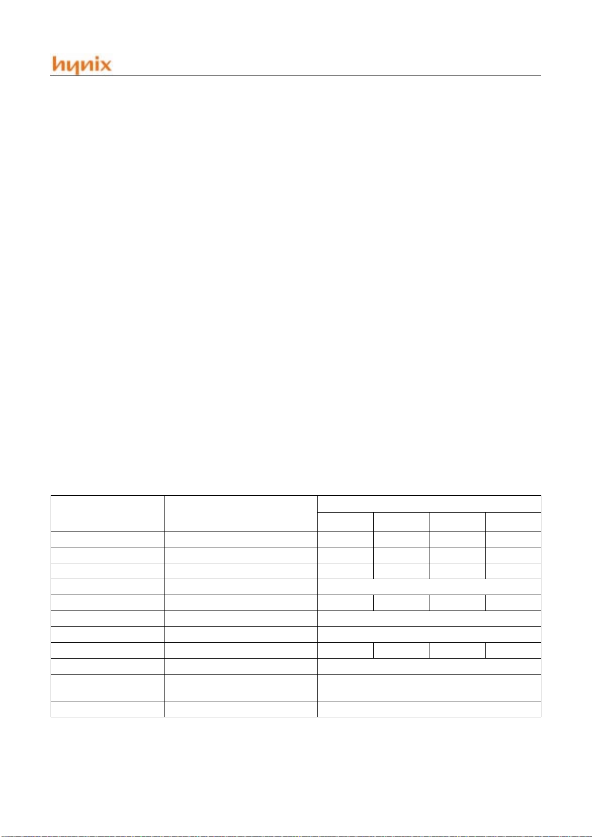
The arithmetic instructions is listed in Table 3-1. The table indicates the addressing modes that can be used with each instruction
to access the <byte> operand. For example, the ADD A, <byte>
instruction can be written as:
ADD a, 7FH (direct addressing)
ADD A, @R0 (indirect addressing)
ADD a, R7 (register addressing)
ADD A, #127 (immediate constant)
Note that any byte in the internal Data Memory space can be incremented without going through the Accumulator.
One of the INC instructions operates on the 16-bit Data Pointer.
The Data Pointer is used to genera te 16-b it addre sses for extern al
memory, so being able to increment it in one 16-bit operations is
a useful feature.
The MUL AB instruction multiplies the Accumulato r by the data
in the B register and puts the 16-bit product into the concatenated
B and Accumulator registers.
The DIV AB instruction divides the Accumulator by the data in
the B register and leaves the 8-bit quotient in the Accumulator,
and the 8-bit remainder in the B register.
MNEMONIC OPERATION ADDRESSING MODES
Dir Ind Reg Imm
ADD A,<byte> A = A+<byte> X X X X
ADDC A,<byte> A = A+<byte>+C X X X X
SUBB A,<byte> A = A-<byte>-C X X X X
IN C A = A+1 Accumulator only
INC <byte> <byte> = <byte>+1 X X X
INC DPTR DPTR = DPTR+1 Data Pointer only
DEC A A = A-1 Accumulator only
DEC <byte> <byte> = <byte>-1 X X X
MUL AB B:A = B x A ACC and B only
DIV AB
DA A Decimal Adjust Accumulator only
A = Int[A/B]
B = Mod[A/B]
Table 3-1 HMS9XC8032 Arithmetic Instructions
ACC and B only
NOV., 2001 Ver 1.02 9

HMS91C8032/97C8032
Oddly enough, DIV AB finds less use in arithmetic "divide" routines than in radix conversions and programmable shift operations. An exam ple of the use of DIV AB in a ra dix conver sion will
be given later. In shift operations, dividing a number by 2n shifts
its n bits to the right. Using DIV AB to p erform the div ision completes the shift in 4µs and leaves the B register holding the bits
that were shifted out. The DA A instructio n is for BCD arithmetic
operations. In BCD arithmetic, ADD and ADDC instructions
should always be followed by a DA A op eration, to ensure that
the result is also in BCD. Note th at DA A will n ot convert a bi nary number to BCD. The DA A operation prod uces a meaning ful
The addressing modes tha t can be used to a ccess t he <b yte> o perand are listed in Table 3-2.
The ANL A, <byte> instruction may take any of the forms:
ANL A,7FH(direct addressing)
ANL A, @R1 (indirect addressing)
ANL A,R6 (register addressing)
ANL A,#53H (immediate constant)
Note that Boolean operations can be performed on any byte in the
internal Data Memory space without going throug h the Accumulator. The XRL <byte>, #data instruction, for example, offers a
quick and easy way to invert port bits, as in
XRL P1, #0FFH.
result only as the second step in the addition of two BCD bytes.
3.4 Logical Instructions
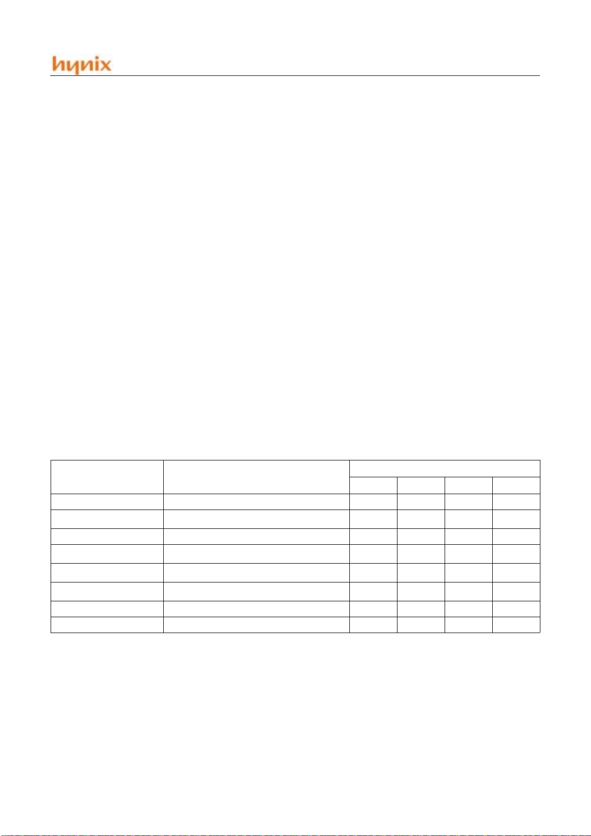
Table 3-2 shows list of HMS9XC8032 logical instructions. The
instructions that perform Boolean operations (AND, OR, Exclusive OR, NOT) on bytes perf orm t he opera tion on a bit-by -bit basis. That is, if the Accumulator contains 0011 0101B and byte
contains 01010011B, then :
ANL A, <byte>
will leave the Accumulator holding 00010001B.
If the operation is in response to an in terrupt, n ot using th e Accu mulator saves the time and effort to push it onto the stack in the
service routine.
The Rotate instructions (RL A, RLC A, etc.) shift the Accumulator 1 bit to the left or right. For a left rotation, the MSB rolls into
the LSB position. For a righ t rotation, the LSB rolls i nto the MSB
position.
The SWAP A instruc tion in terchange s the high and low ni bbles
within the Accumulator. This is a useful operation in BCD manipulations. For example, if the Accumulator contains a binary
number which is known to be less than 100, it can be quickly converted to BCD by the following code:
MNEMONIC OPERATION ADDRESSING MODES
Dir Ind Reg Imm
ANL A,<byte> A = A .AND. <byte> X X X X
ANL <byte>,A <byte> = <byte> .AND. A X
ANL <byte>,#data <byte> = <byte> .AND. #data X
ORL A,<byte> A = A .OR. <byte> X X X X
ORL <byte>,A <byte> = <byte> .OR. A X
ORL <byte>,#data <byte> = <byte> .OR. #data X
XRL A,<byte> A = A .XOR. <byte> X X X X
XRL <byte>,A <byte> = <byte> .XOR. A X
XRL <byte>,#data <byte> = <byte> .XOR. #data X
CRL A A = 00H Accumulator only
CPL A A = .NOT. A Accumulator only
RL A Rotate ACC Left 1 bit Accumulator only
RLC A Rotate Left through Carry Accumulator only
RR A Rotate ACC Right 1 bit Accumulator only
RRC A Rotate Right through Carry Accumulator only
SWAP A Swap Nibbles in A Accumulator only
Table 3-2 HMS9XC8032 Logical Instructions
10 NOV., 2001 Ver 1.02
HMS91C8032/97C8032
MOVE B,#10
DIV AB
SWAP A
ADD A,B
Dividing the number by 1 0 lea ves th e tens d igit in the low nibble
of the Accumulator, and the ones digit in the B register. The
SWAP and ADD instructions move the tens digit to the high nibble of the Accumulator, and the ones digit to the low nibble.
3.5 Data Tr ansfers
Internal RAM
Table 3-3 shows the menu of instructions that are available for
moving data around within the internal memory spaces, and the
addressing modes that can be used with each one.
The MOV <dest>, <src> instruction allo ws data to be transferred
between any two internal RAM or SFR locations without going
through the Accumulator. Remember, the Upp er 128 bytes of
data RAM can be accessed only by indirect addressing, and SFR
space only by direct addressin g.
Note that in HMS9XC8032 devices, the stack res ides in on-chi p
RAM, and grows upwards. The PUSH instruction first increments the Stack Pointer (SP), then copies the byte into the stack.
PUSH and POP use only direct addressing to identify the byte being saved or restored, but t he stack itsel f is accessed by i ndirect
addressing using the SP register. This means the stack can go into
the Upper 128 bytes of RAM, if they are implemented, but not
into SFR space.
The Data Transfer instructions include a 16 -b it MOV th at can b e
used to initialize the Data Pointer (DPTR) for look-up tables in
Program Memory.
The XCH A, <byte> instruction causes the Accumulator and addressed byte to exchange data. The XCHD A, @Ri instruction is
similar, but only the low nibbles are involved in the exchange.
To see how XCH and XCHD can be used to facilitate da ta manipulations, consider first the problem of shifting and 8-digit BCD
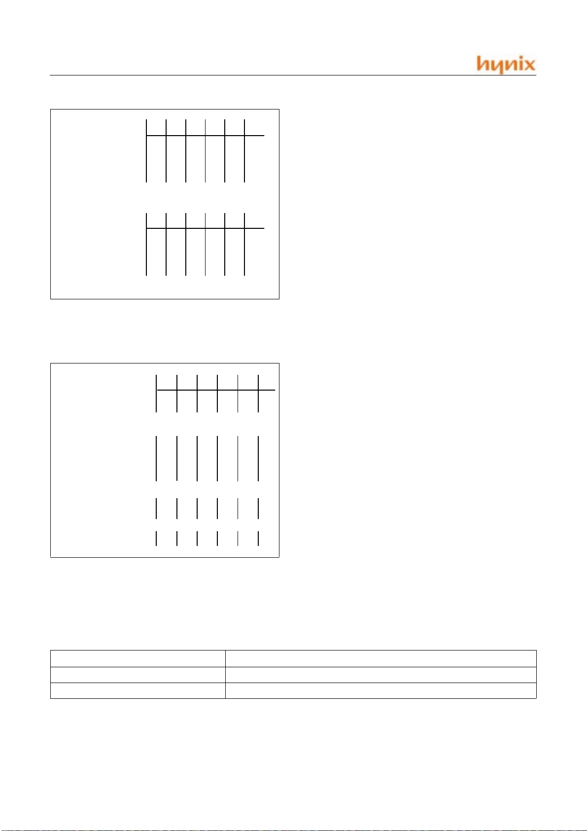
number two digits to the right. Figure 3-2 shows how this can be
done using XCH instructions. To aid in understanding how the
code works, the contents of the registers that are holding the BCD
number and the content of the Accumulator are shown alongside
each instruction to indicate their status after the instruction has
been executed.
After the routine has been executed, the Accumulator contains
the two digits that were shifte d out on th e right. Doin g the routin e
with direct MOVs uses 14 code bytes. The sa me operation with
XCHs uses only 9 bytes and execut es almost twice as fast.
To right-shift by an odd number of digits, a one-digit must be executed.
Figure 3-3 shows a sample of code that will right-shift a BCD
number one digit, using the XCHD instruction. Again, the contents of the registers holding the number and of the accumulator
are shown alongsid e each instruction.
MNEMONIC OPERATION ADDRESSING MODES
Dir Ind Reg Imm
MOV A,<src> A = <src>
MOV <dest>,A <dest> = A
MOV <dest>,<src> <dest> = <src>
MOV DPTR,#data16 DPTR = 16-bit immediate constant
PUSH <src> INC SP:MOV “@SP”, <src>
POP <dest> MOV <dest>, “@SP”:DEC SP
XCH A,<byte> ACC and <byte> exchange data X X X
XCHD A,@Ri ACC and @Ri exchange low nibbles X
Table 3-3 Data Transfer Instruction that Access Internal Data Memory Space
XXXX
XXX
XXXX
X
X
X
NOV., 2001 Ver 1.02 11
HMS91C8032/97C8032
2B
2A
12
MOV A,2EH
MOV 2EH,2DH
MOV 2DH,2CH
MOV 2CH,2BH
MOV 2BH,#0
A. Using d irect MOVs: 14 bytes, 9 us
CLR A
XCH A,2BH
XCH A,2CH
XCH A,2DH
XCH A,2EH
B. Using XCHs: 9 bytes, 5us
00
12
00
12
00
12
00
00
00
2B
2A
12
00
00
00
00
00
00
00
00
00
Figure 3-2 Shifting a BCD Number Two Digits to the
Right
2A
MOV R1,#2EH
MOV R0,#2DH
00
00
2D 2E ACC
2C
78
56
34
56
34
34
34
34
12
34
12
2D 2E ACC
2C
56
34
56
34
56
12
34
12
34
12
2D 2E
2C
2B
1212343456567878XX
78
56
78
56
78
56
78
56
78
78
00
78
12
78
34
78
56
56
78
ACC
XX
leaves the last byte, location 2EH, holding the last two digits of
the shifted number. The p ointers are decre mented, and the loop is
repeated for location 2DH. The CJNE instruction (Compare and
Jump if Not equal) is a loop control that will be described later.
The loop executed from LOOP to CJNE for R1 = 2EH, 2DH,
2CH, and 2BH. At that point the digit that was originally shifted
out on the right has pr opagated to location 2AH. Since that location should be left with 0s, the lost di git is moved to the Accum ulator.
External RAM
HMC9XC8032 series do NOT support external RAM access
mode.
3.6 Lookup Tables
Table 3-4 shows the two instructions that are available for reading lookup tables in Program Memory. Since these instructions
access only Program Memory, the lookup tables can only be read,
not updated.
The mnemonic is MOVC for "move constant." The first MOVC
instruction in Table 3-1 can accommodate a table of up to 256 entries numbered 0 through 25 5. T he numbe r of the desired entry is
loaded into the Accumu lator, and the Data Poi nter is set up to
point to the beginning of the table. Then:
MOVC A, @A+DPTR
loop for R1 = 2EH
MOV A,@R1
LOOP:
XCHD A,@R0
SWAP A
MOV @R1,A
DEC R1
DEC R0
CJNE R1,#2AH,LOOP
00
12
00
12
00
12
00
12
00
12
00
12
56
34
58
34
58
34
58
34
58
34
58
34
78
78
76
78
67
78
67
67
67
67
67
67
copies the desired table entry into the Accumulator.
The other MOVC instruction works the same way, exce pt the
Program Counter (PC) is used as the t able base, and the table is
accessed through a subroutine. First the number of the desired entry is loaded into the Accumulator, and the subroutine is called:
MOV A , ENTRY NUMBER
loop for R1 = 2DH:
loop for R1 = 2CH:
loop for R1 = 2BH:
CLR A
XCH A,2AH
00
00
08
000801
38
12
23
18
23
01
23
01
23
67
45
45
45
45
45
45
67
23
67
01
67
00
67
08
CALL TABLE
The subroutine "TABLE" would look like this:
TABLE: MOVC A , @A+PC
RET
Figure 3-3 Shifting a BCD Number One Digits to the
Right
The table itself immediately follows the RET (re turn ) instruc ti on
is Program Memory. This type of table can hav e up to 255 entries,
numbered 1 through 255. Number 0 cannot be used, because at
the time the MOVC instruction is executed, the PC contains the
First, pointers R1 and R0 are set up to point to the two bytes con taining the last four BCD digits. Then a loop is executed which
address of the RET instruction. An entry numbered 0 would be
the RET opcode itself.
MNEMONIC OPERATION
MOVC A, @A+DPTR Read program memory at (A + DPTR)
MOVC A, @A+PC Read program memory at (A + PC)
Table 3-4 Table B-4 HMS9XC8032 Data Transfer Instruction that Access Internal Data Memory Spcace
12 NOV., 2001 Ver 1.02

3.7 Boolean Instructions
HMS9XC8032 devices contain a complete Boolean (single-bit)
processor. One page of the int ernal RAM contains 128 addressable bits, and the SFR space can support up to 128 addressab le
bits as well. All of the port lines are bit-addressable, and each one
can be treated as a separate single-bit port. The instructions that
access these bits are not just conditional branches, but a complete
menu of move, set, clear, com plement, OR and AND instructions. These kind s of bi t operat ions ar e not ea sily obt ained in other architectures with any amount of byte-oriented software.
The instruction set for the Boolean processor is shown in Table
3-5. All bits accesses are by direct ad dressing.
Bit addresses 00H through 7FH are in the Lower 128, and b it addresses 80H through FFH are in SFR space.
Note how easily an inte rna l fl a g can be mo ve d to a port pin:
MOV C,FLAG
MOV P1.0,C
In this example, FLAG is the name of any addressable bit in the
Lower 128 or SFR space. An I/O line (the LSB of Port 1, in this
case) is set or cleared depending on whether the flag bit is 1 or 0.
HMS91C8032/97C8032
Note that the Boolean instruction set includ es ANL and ORL op-
erations, but not the XRL (Exclusive OR) operation. An XRL op-
eration is simple to implement in software. Suppose, fo r example,
it is required to form the Exclusive OR of two bits:
C = bit 1 .XRL. bit2
The software to do that could be as follows:
MOV C , bit1
JNB bit2, OVER
CPL C
OVER: (continue)
First, bit1 is moved to th e Car ry. If bit2 = 0, then C n ow co nta in s
the correct result. That is, bit1 .XRL. bit2 = bit1 if bit2 = 0. On
the other hand, if bit2 = 1, C now contains the complement of the
correct result. It need only be inverted (CPL C) to complete the
operation.
This code uses the JNB instruction, one of a series of bit-test in-
structions which execute a jump if the addressed bi t is set (JC, JB,
JBC) or if the addressed bit is not set (JNC, JNB). In the above
case, bit2 is being tested, and if bit2 = 0, the CPL C instruction is
jumped over.
The Carry bit in the PSW i s used as the sin gle-bit Accumul ator of
the Boolean processor. Bit instructions that refer to the Carry bit
as C assemble as Carry-specific instructions (CLR C, etc.). The
Carry bit also has a direct address, since it resides in the PSW register, which is bit-addressable.
MNEMONIC OPERATION
ANL C,bit C = A .AND. bit
ANL C,/bit C = C .AND..NOT. bit
ORL C,bit C = A .OR. bit
ORL C,/bit C = C .OR..NOT. bit
MOV C,bit C = bit
MOV bit,C bit = C
CLR C C = 0
CLR bit bit = 0
SETB C C = 1
SETB bit bit = 1
CPL C C = .NOT.C
CPL bit bit = .NOT.bit
JC rel Jump if C = 1
JNC rel Jump if C = 0
JB bit,rel Jump if bit = 1
JNB bit,rel Jump if bit = 0
JBC bit,REL Jump if bit = 1;CLR bit
Table 3-5 Table B-5 HMS9XC8032 Boolean Instructions
JBC executes the jump if the addresse d bit is set , and also clears
the bit. Thus a flag can be tested and cleared in one operation. All
the PSW bits are directly addressable, so th e Parity bit, or the gen-
eral-purpose flags, for example, are a lso available to the bit-test
instructions.
3.8 Relative Offset
The destination address for these jumps is specified to the assem-
bler by a label or by an actual address in Program memory. How-
ever, the destination address assembles to a relative offset byte.
This is a signed (two's complement) offset byte which is added to
the PC in two's complement arithmetic if the jump is executed.
The range of th e jump is the refore - 128 to +127 Program Me mory
bytes relative to the first byte following the instruction.
3.9 Jump Instructions
Table 3-6 shows the list of unconditional jumps.
MNEMONIC OPERATION
JMP addr Jump to addr
JMP @A+DPTR Jump to A+DPTR
CALL addr Call subroutine at addr
RET Return from subroutine
RETI Return from interrupt
NOP No operation
Table 3-6 Unconditional Jumps in HMS9XC8032
Devices
NOV., 2001 Ver 1.02 13

HMS91C8032/97C8032
The table lists a single "JMP add" instruct ion, but in fact there are
three SJMP, LJMP, and AJMP, which differ in the format of the
destination address. JMP is a generic mnemonic which can be
used if the programmer does not care which way the jump is encoded.
The SJMP instruction encodes the destination address as a relative offset, as described above. The instruction is 2 bytes long,
consisting of the opcode and the relative offset byte. The jump
distance is limited to a range of -128 to +12 7 bytes relative to the
instruction following the SJMP.
The LJMP instruction encodes the destination address as a 16-bit
constant. The instruction is 3 bytes long , consisting o f the opcode
and two address bytes. Th e dest inati on ad dress c an b e an ywhe re
in the 64K Program Memory space.
The AJMP instruction encodes the destination add ress as an
11-bit constant. The instruction is 2 bytes long, consisting of the
opcode, which itself contains 3 of the 11 address bits, followed by
another byte containing the low 8 bits of the de stination address.
When the instruction i s ex ecu te d, the s e 11 b its a re si mply sub s tituted for the low 11 bits in the PC. The hig h 5 bits sta y the same .
Hence the destination has to be within the same 2K block as the
instruction following the AJMP.
In all cases the programmer specifies the destination address to
the assembler in the same way: as a label or as a 16-bit constant.
The assembler will put the destination address into the correct
format for the given instruction. If the format required by the instruction will not support t he di stance to the specified destin ation
address, a "Destination out of range" message is written into the
List file.
Table 3-1 shows a single "CALL addr" instruction, but there are
two of them, LCALL and ACALL, which differ in the format in
which the subroutine address is give n to the CPU. CALL is a g e-
neric mnemonic whi ch can be used if the progr ammer does not
care which way the address is encoded.
The LCALL instruction uses the 16-bit address format, and the
subroutine can be anywhere in the 64K P r ogram Memory space.
The ACALL instruction uses the 11-bit format, and the subrou-
tine must be in the same 2K b lock as the i nstruction fo llowing the
ACALL.
In any case, the programmer specifies the subroutine address to
the assembler in the same way: as a label or as a 16-bit constant.
The assembler will put the address into the correct form at for th e
given instructions .
Subroutines should end with a RET instruction, which returns ex-
ecution to the instruction following the CALL.
RETI is used to return from an interrupt service routine . The only
difference between RET and RETI is that RETI tells the interrupt
control system that the interrupt in progress is done. If there is no
interrupt in progress at the time RETI is exec ut ed, th en th e RETI
is functionally identical to RET.
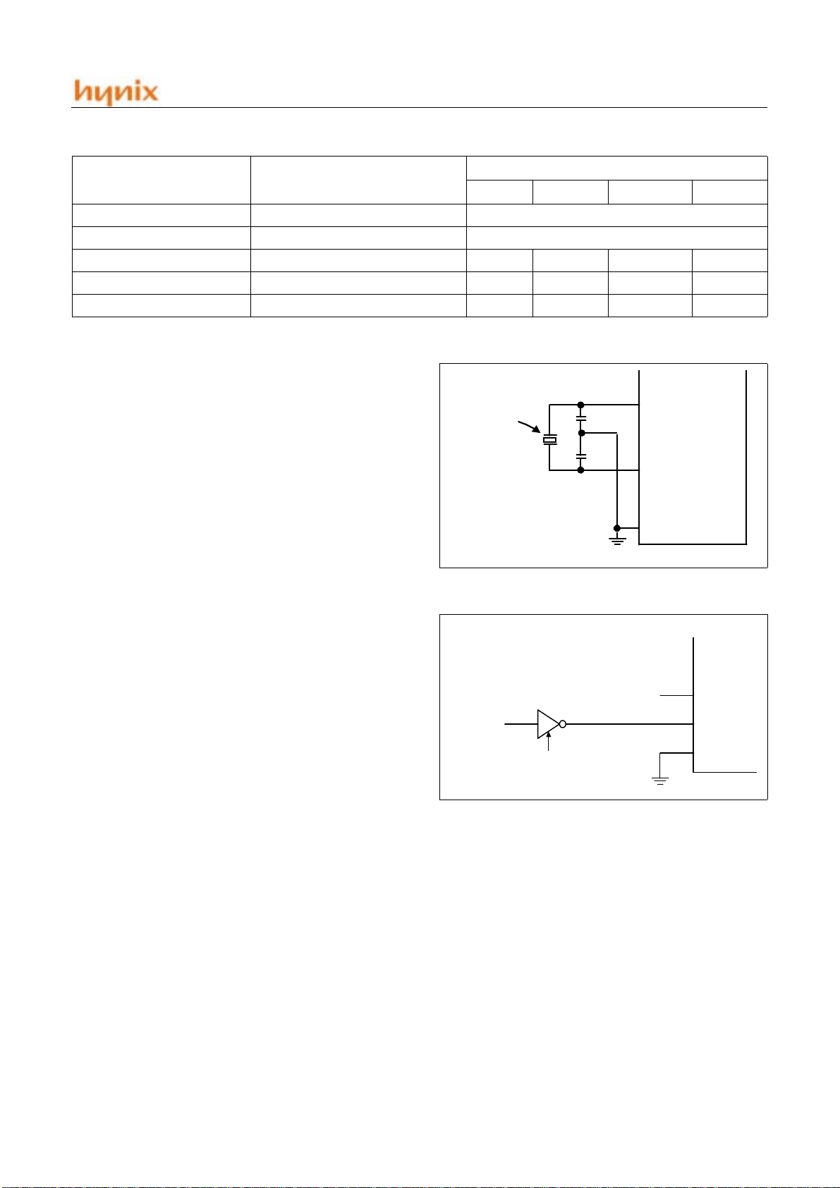
Table 3-7 shows the list of conditional jumps available to the
HMS9XC8032 user. All of these jumps specify the destination
address by the relative offset me thod, and so are limi ted to a jump
distance of -128 to +127 bytes from the instruction following the
conditional jump instruction. Im portant to note, however, th e user
specifies to the assembler the actual destination address the same
way as the other jumps: as a label or a 16-bit constant.
The JMP @A+DPTR instruction supports case jumps. The destination address is computed at exec ution time as the su m of the
16-bit DPTR register and the Accumulator. Typically. DPTR is
set up with the address of a jump table. In a 5-way branch, for example, an integer 0 thro ugh 4 is loade d into the Accumul ator. The
code to be executed might be as follows:
MOV DPTR,#JUMP TABLE
MOV A,INDEX_NUMBER
RL A
JMP @A+DPTR
The RL A instruction converts the index number (0 through 4) to
an even number on the r ange 0 thro ugh 8, be cause eac h entry in
the jump table is 2 bytes long:
JUMP TABLE:
AJMP CASE 0
AJMP CASE 1
AJMP CASE 2
AJMP CASE 3
AJMP CASE 4
There is no Zero bit in t he PSW . The JZ an d JNZ instruc tions test
the Accumulator data for that condition.
The DJNZ instruction (Decrement and Jump if Not Zero) is for
loop control. To execute a loop N times, load a counter byte with
N and terminate the loop with a DJNZ to the beginning of the
loop, as shown below for N = 10:
MOV COUNTER,#10
LOOP:(begin loop)
•
•
•
(end loop)
DJNZ COUNTER, LOOP
(continue)
.
The CJNE instruction (Compare and Jump if Not Equal) c an also
be used for loop control as in F igure 12. Two bytes are specified
in the operand field o f th e instru c tio n. The j um p is exe cute d on ly
if the two bytes are not equal. In the example of Figu re B-3 Shift-
ing a BCD Number One Digits to the Right, the two bytes were
data in R1 and the constant 2 AH. The initia l data in R1 was 2EH.
14 NOV., 2001 Ver 1.02
HMS91C8032/97C8032
MNEMONIC OPERATION ADDRESSING MODES
DIR IND REG IMM
JZ rel Jump if A = 0 Accumulator only
JNZ rel Jump if A ≠ 0 Accumulator only
DJNZ <byte>,rel Decrement and jump if not Zero X X
CJNE A,<byte>,rel Jump if A ≠ <byte> X X
CJNE <byte>,#data,rel Jump if <byte> ≠ #data X X
Table 3-7 Conditional Jumps in HMS9XC8032 Devices
Every time the loop was executed, R1 was d ecremented, and the
looping was to continue until the R1 data reached 2AH.
XTAL2
Another application of this instruction is in "greate r than, less
than" comparisons. The two bytes in the operand field are taken
as unsigned integers. If the first is less than the second, then the
Carry bit is set (1). If the first is greater than or equal to the second, then the Carry bit is cleared
Quartz crysta l
or ceramic
resonator
C1
C2
Xout (XTout)
Xin (XTin)
XTAL1
3.10 CPU Timing
All HMS9XC8032 microcontrollers have an on-chip oscillator
which can be used if desired as the clock source for the CPU. To
use the on-chip oscillator, connect a crystal or ceramic resonator
between the Xout (XTout) an d Xin(XTin) pi ns of the mi crocontroller, and capacitor s to gr ound as sh own in F igure 3-4 Using the
On-Chip Oscillator.
Examples of how to drive the clock with an extern al oscillato r are
shown in Figure 3-5 . In the CMOS dev ices (HMS9XC80 32, etc.) ,
the signal at the Xout(XTout) pin drives the internal clock generator. The internal clock ge nerat or defi nes t he sequ ence o f st ates
that make up the HMS9XC80 32 machine cycle.
Main Clock
Xin, Xout : 7.2 MHz
Sub Clock
XTin, XTout : 32.768 KHz
Figure 3-4 sing the On-Chip Oscillator
EXTERNAL
OSCILLATOR
SIGNAL
CMOS GATE
Figure 3-5 Using an External Clock
Vss
DTS3
NC
XTAL1
Xout (XTout)
XTAL2
Xin (XTin)
Vss
NOV., 2001 Ver 1.02 15
HMS91C8032/97C8032
3.1 1 Machine Cycles
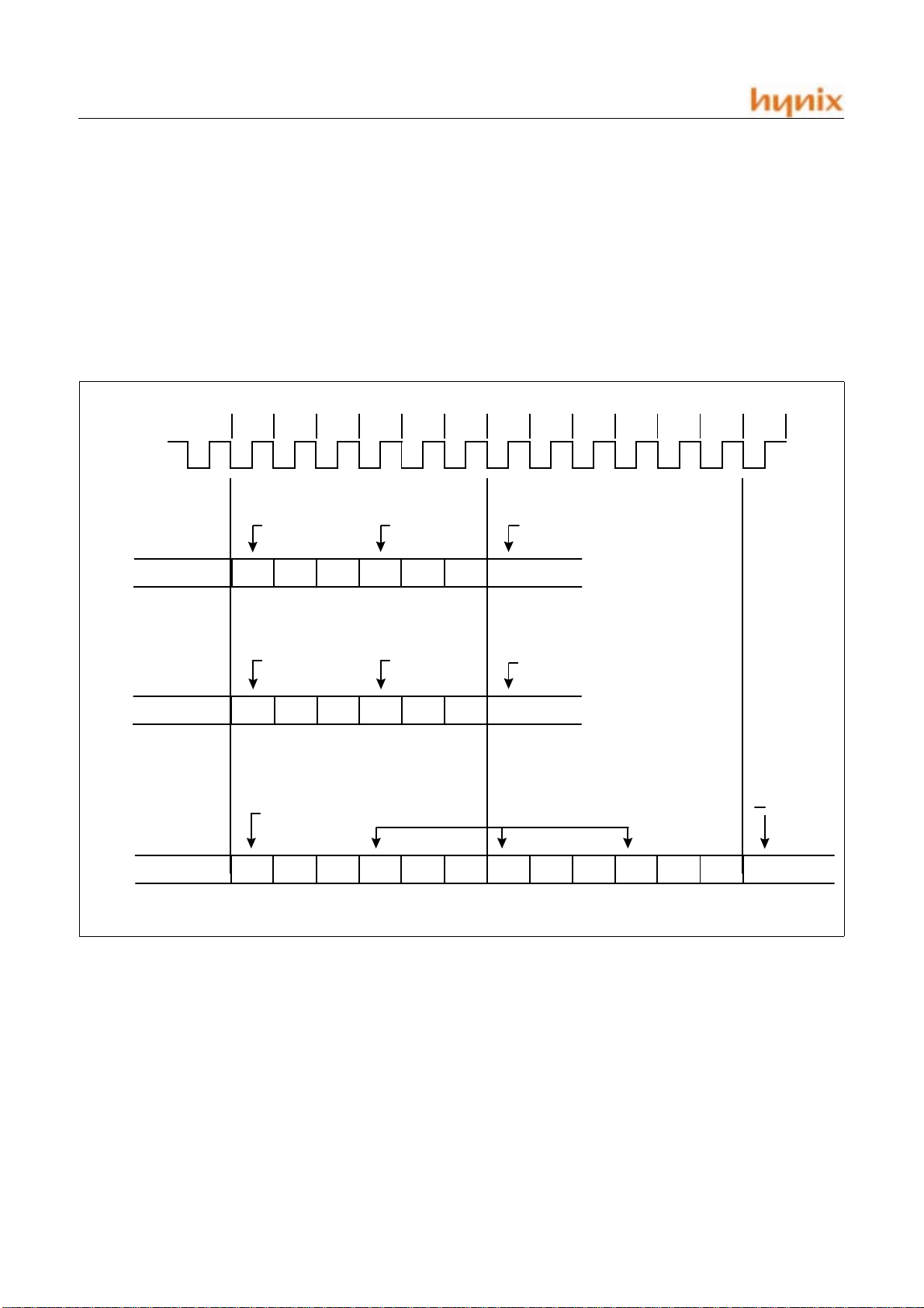
A machine cycle consists of a sequence of 6 states, numbered S1
through S6. One machine cycle period vary according to the SCMOD register value. Refer to Figure 3-6
Each state is divided into a Phase 1 half and a Phase 2 half. State
Sequence in HMS9XC8032 Devices shows that fetch/execute sequences in states and phases for vari ous kinds of instructi ons.
Normally two progra m fetches are gene rated during each machine cycle, even if the instruction being executed doesn't require
it. If the instruction being executed doesn't need more code bytes,
the CPU simply ignores the e xtra fetc h, a nd the Pro gram Coun ter
is not incremented.
Execution of a one-cycle instruction (Figure 3-6) begins during
State 1 of the machine cycle, when th e opc od e is latche d into the
Instruction Register. A second fetch occurs during S4 of the same
machine cycle. Execution is complete at the end of State 6 of this
machine cycle.
Osc.
CPU Clock
(XTAL2)
(f
)
CPU
S1 S2 S3 S4 S5 S6 S1 S2 S3 S4 S5 S6 S1
P1P2 P1P2 P1P2 P1P2 P1P2 P1P2 P1P2 P1P2 P1P2 P1P2 P1P2 P1P2
Read opcode.
S1
S2
S3
S4
a. 1-byte, 1-cycle instruction, e.g., INC A
Read opcode.
S1
S2
S3
S4
b. 2-byte, 1-cycle Instruction, e.g., ADD A, #data
Read opcode.
Read next
opcode
(discard).
S5
S6
Read 2nd byte.
S5
S6
Read next
opcode (discard)
P1P2
Read next opcode again.
Read next opcode.
Read next opcode again.
S1
S2
S3
S4
S5
S6
S1
S2
S3
S4
S5
S6
c. 1-byte, 2-cycle instruction, e.g., INC DPTR
Figure 3-6 State Sequence in HMS9XC8032 Devices
16 NOV., 2001 Ver 1.02
HMS91C8032/97C8032
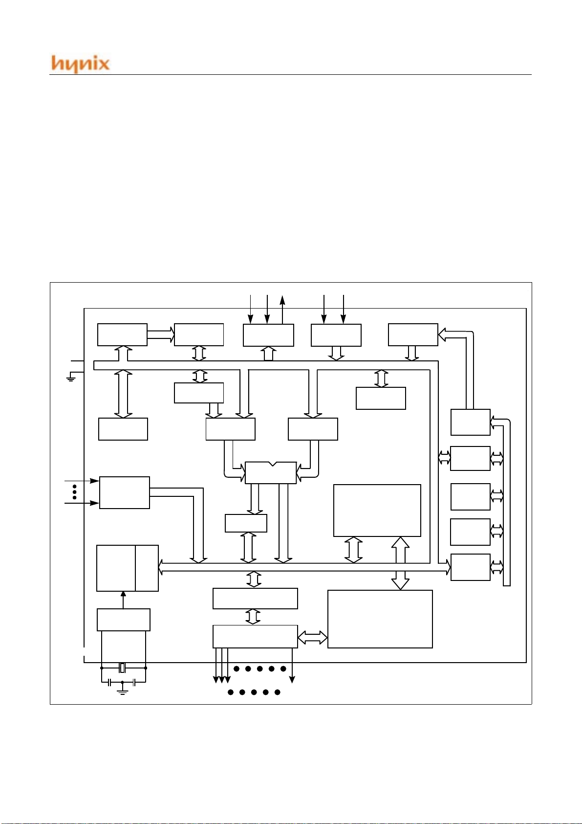
4. HARDWARE DESCRIPTION
This chapter provides a detailed description of the HMS9XC8032 microcontroller (see Figure 4-1) included in this description are the:
• Clock Genernation Block
• IF Counter
• Special Function Registers
• Timers/Counters
• Serial Interface (UART)
• Standard Serial Interface (SI0 1, SIO2)
• Port Structure
• Watch Dog Timer
•Buzzer
RAM Address
Register
Vcc
Vss
B
Register
RAM
ACC
TMP2 TMP1
•PLL
• ADC
• Interrupts
• Reset
• Power-On Reset
• Power-Saving Modes
• On-Chip Oscillators
Stack
Pointer
ROM
Program
Address
Register
XTAL1
Timing
And
Control
Oscillator
Instruction
XTAL2
Buffer
ALU
PC
Peripheral Control
PSW
Register
Register Blocks
Incrementer
Program
Counter
DPTR
Ports Latchs
Peripheral Blocks
(Interrupt, SIOs, Timers, etc)
Ports Drivers
P0 P7
Figure 4-1 HMS9XC8032 Architecture
NOV., 2001 Ver 1.02 17
HMS91C8032/97C8032
4.1 Clock Generation Block
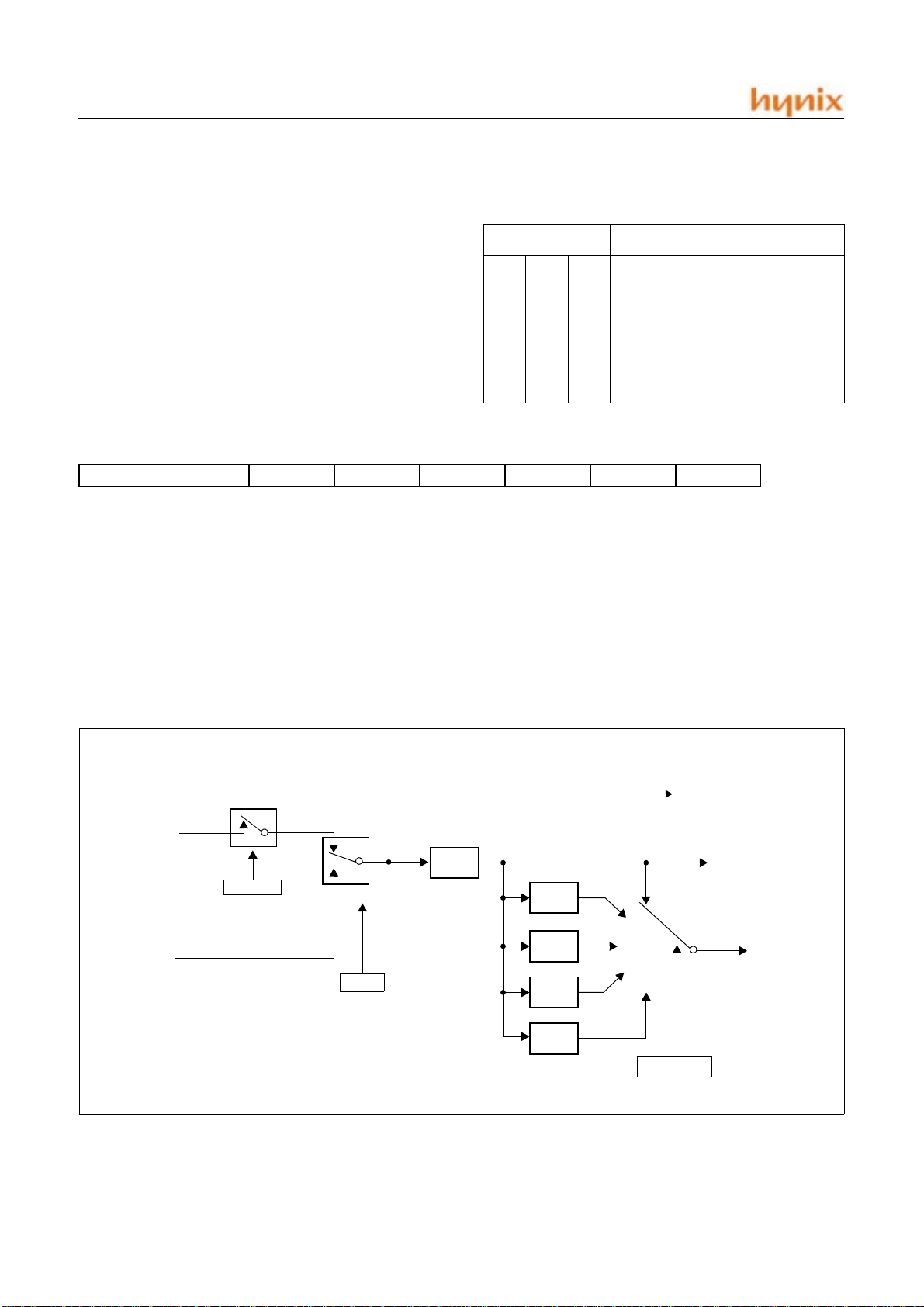
Software can control the system clock speed of HMS91C8032
with the SCMOD register. the SCMOD register determine system clock speed and clock source. Figure 4-3 shows the block diagram of the system clo c k generation block.
Guideline on the CPU clock speed
For determining the speed of CPU clock(f
constraints should be satisfied.
The maximum counting rate of timer0~4 in counter mode,
should be less than or equal to (1/6)f
CPU
The maximum timer clock rate of timer0~4 in timer mode
should be less than or equal to (1/2)f
CPU
), the following
CPU
SCMOD: SELECT CLOCK MODE. : 80H
- - - SCSTOP SCSW SCMOD2 SCMOD1 SCMOD0
- SCMOD.7 Reserved for future use *
- SCMOD.6 Reserved for future use *
- SCMOD.5 Reserved for future use *
SCSTOP SCMOD.4 Software control of the main system oscillator. A logic 1 pulls down the main
system oscillator (7.2MHz).
SCSW SCMOD.3 Software switch control betwee n main system oscillator and sub syst em oscillator.
A logic 1 switches sub syst em oscillator (32.768KHz).
SCMOD2 SCMOD.2 See NOTES
SCMOD1 SCMOD.1 See NOTES
SCMOD0 SCMOD.0 See NOTES
NOTE:
SCMOD[2:0] Select system clock
0xxfxx
1 0 0 fxx / 2
1 0 1 fxx / 4
1 1 0 fxx / 8
1 1 1 fxx / 16
PLL Clock
f
MOSC
(Main Oscillator Clock)
f
SOSC
(Sub Oscillator Clock)
SCSTOP
0
1
SCSW
f
OSC
(Oscillator
Clock)
1/2
f
XX
1/2
1/4
1/8
1/16
SCMOD1 ,2 ,3
Watchdog Clock
f
CPU
(CPU Clock)
Figure 4-2 System Clock Generation Block
18 NOV., 2001 Ver 1.02
4.2 Special Function Registers
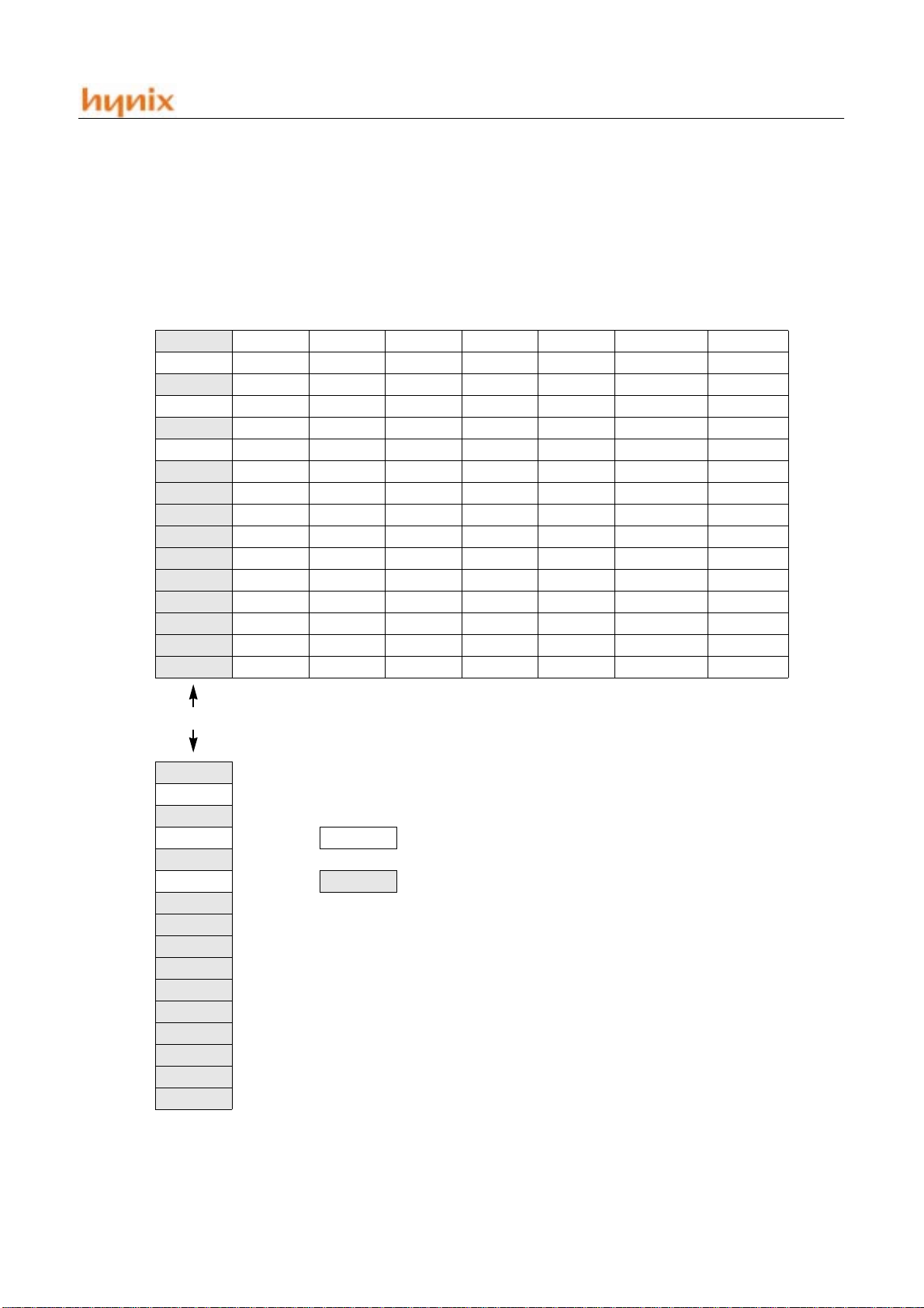
A map of the on -chip memory area called the Specia l Function
Register (SFR) space is shown in Table 4-1 and Table 4-2. Note
that in the SFRs not all of the addresses are occupied. Unoc cupied
addresses are not implemented on the chip. Read accesses to
these addresses will in general return random data, and write accesses will have no effect.
HMS91C8032/97C8032
User software should not write 1s to these unimplemented locations, sinc e they ma y be used in other H MS9XC8032 F amily
products to invoke new fe atures. In th at case th e reset or inac tive
values of the new bits will always be 0, and their active values
will be 1.
F8
F0 B PLLMOD PLLDRH PLLDRL IFCMOD IFCDR2 IFCDR1 IFCDR0 F7
E8 IR3 EF
E0 ACC E7
D8
D0 PSW D7
C8 T2CON RCAP2L RCAP2H TL2 TH2 CF
C0
B8 IP P4MOD P5MOD P6MOD P7MOD BF
B0 IE2 IP2 P0MOD P1MOD P2MOD P3MOD B7
A8
A0 S12CON SBUF1 SBUF2 P0CON P1CON P2CON P3CON A7
98 SCON SBUF 9F
90
88 TCO N TMOD TL0 TL1 TH0 TH1 8F
80 SCMOD SP DPL DPH ADCCON ADCDR PLLDEBUG PCON 87
F8
F0 B
E8 P6DATA
E0 ACC
D8
D0 PSW
C8
C0
B8 P3DATA
B0
A8 P2DATA
A0
98 P1DATA
90
88 P0DATA
80
WDTCON WDTDR RDPG WRPG SFRPG FF
IR2 IT2 DF
IE3 IP3 C7
IE P4CON P5CON P6CON P7CON AF
T34CON T34MOD TL3 TL4 TH3 TH4 97
Table 4-1 SFRPG0 SFR Memory Map (8 Bytes)
Bit Addressable
P7DATA
: in this area, the registers of SFRPG0 are the sam e regi sters of SFRPG1
P5DATA
: in this area, the registers of SFRPG0 are different from registers of SFRPG1
P4DATA
Table 4-2 SFRPG1 SFR Memory Map (8 Bytes)
NOV., 2001 Ver 1.02 19

HMS91C8032/97C8032
(MSB)
CY AC F0 RS1 RS0 OV - P
Symbol
CY
AC
F0
RS1
RS0
OV
-
P
NOTE: The contents of (RS1, RS0) enable the working register bank as follows:
Position
PSW.7
PSW.6
PSW.5
PSW.4
PSW.3
PSW.2
PSW.1
PSW.0
(0,0) - Bank 0 (00H-07H)
(0,1) - Bank 1 (08H-0FH)
(1,0) - Bank 2 (10H-17H)
(1,1) - Bank 3 (18H-1FH)
Name and Significance
Carry Flag.
Auxiliary Catrry flag. (For BCD Operations.)
Flag 0. (Available to the user for general purposes.)
Register bank select control bit 1.
Set/clear by software to determine working register bank. (See Note.)
Register bank select control bit 0.
Set/clear by software to determine working register bank. (See Note.)
Overflow flag.
User-definable flag.
Parity flag.
Set/cleared by hardware each instruction cycle to indicate an odd/even
number of "one" bits in the Accumulator, i.e., even parity.
Figure 4-3 Program Status Word (PSW) Register
(LSB)
Accumulator
ACC is the Accumulator register. The mnemonics for accumula-
tor-specific instructions, however, refer to the accumulator simply as A.
B Register
The B register is u s e d d uring multiply and divide operati on s . Fo r
other instructions it can be treated as ano ther scratch pad registe r.
Program Status Word
The PSW register contains program status information as detailed
in Figure 4-3.
Stack Pointer
The Stack Pointer register is 8 bi ts wide . It is in c re mente d b e fore
data is stored during PUSH and CALL executions. While the
stack may reside anywhere in on-chip RAM, the Stack Pointer is
initialized to 07H after a reset. This causes the stack to begin at
locations 08H.
But, it is forbidden to use th e area of 00H to
7FH as the Stack. Thus the stack pointer should be set to the
address larger than 7FH when it is initialized.
Data Pointer
The Data Pointer (DPTR) consists of a high byte (DPH) and a low
byte (DPL). Its intended function is to hold a 16-bit address. It
may be manipulated as a 16-bit register or as two independent
8-bit registers.
Serial Data Buffer
SBUF, SBUF1 and SBUF2 are Serial Buffers. SBUF register is
used by UART, SBUF1 used by SIO1 and SBUF2 used by SIO2.
The SBUF is actually two se parate registers, a transmit buffer a nd
a receive buffer. When data is moved to SBUF, it goes to the
transmit buffer and is held for serial transmission. (Moving a byte
to SBUF is what initiates the transmission.) When data is moved
from SBUF, it comes from the receive buffer.
Unlike SBUF, SBUF1(SBUF2) is one register. If the SIO1(SIO2)
run flag is activated, receive and transmit of serial data is done simultaneously using SBUF1(SBUF2).
Timer Registers Basic to HMS9XC8032
Register pairs (THx, TLx) are the 16-bit Counting regis ters for
Timer/Counters 0, 1, 2, 3 and 4, respectively.
Control Register for the HMS9XC8032
Special Functio n Regist ers IP x, IEx, TMOD, T 34MOD, TCO N,
T2CON, SCON, S12CON, PCON and etc. contain control and
status bits for the various peripherals in HMS9XC8032. They are
described in later sections.
20 NOV., 2001 Ver 1.02
HMS91C8032/97C8032
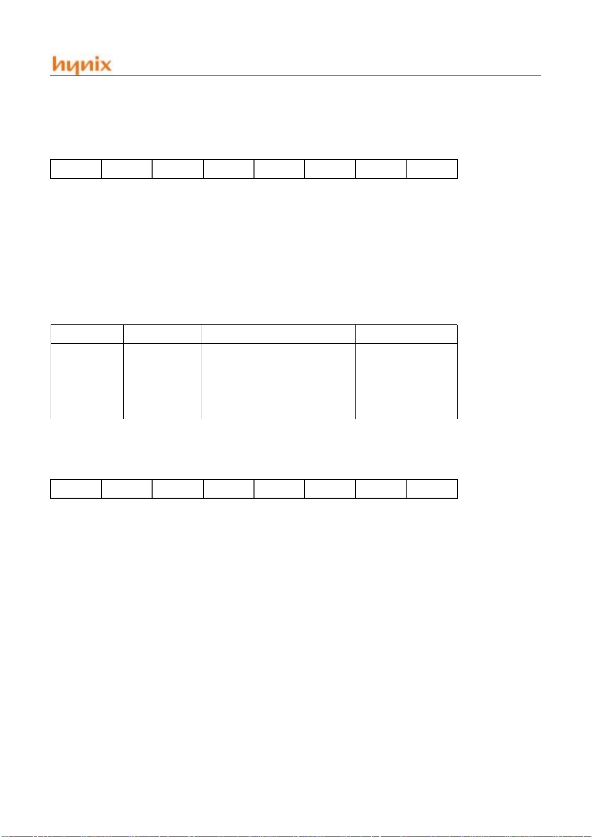
Summary of SFR
PSW: PROGRAM STATUS WORD. BIT ADDRESSABLE. : D0H
CY AC F0 RS1 RS0 OV - P
CY PSW.7 Carry Flag.
AC PSW.6 Auxiliary Carry Flag.
F0 PSW.5 Flag 0 available to the user for ge neral purpose.
RS1 PSW.4 Register Bank selector bit 1 (See NOTE 1).
RS0 PSW.3 Register Bank selector bit 0 (See NOTE 1).
OV PSW.2 Overflow Flag.
- PSW.1 User flag.
P PSW.0 Parity flag. Set/cleared by hardware each instruction cycle to indicate an odd/even number of ‘1’ bits in
th accumulator.
NOTE 1:
The value presented by RS0 and RS1 selects the corresponding register bank.
RS1 RS0 Register Bank Addresss
0 0 0 00H-07H
01 1 08H-0FH
1 0 2 10H-17H
11 3 18H-1FH
PCON: POWER CONTROL REGISTER. NOT BIT ADDRESSABLE. : 87H
SMOD - - - GF1 GF0 PD IDL
SMOD PCON.7 Double baud rate bit. If Timer 1 is used to generate baud rate and SMOD = 1, th e baud rate is doubled
when the Serial Port is used in modes 1, 2, or 3.
- PCON.6 Not implemented, reserved for future use.*
- PCON.5 Not implemented, reserved for future use.*
- PCON.4 Not implemented, reserved for future use.*
GF1 PCON.3 General pu rpose flag bit.
GF0 PCON.2 General pu rpose flag bit.
PD PCON.1 Power Down bit. Setting this bit activates Power Down operation.
IDL PCON.0 dle Mode bit. Setting this bit activates Idle Mode operation.
If 1s are written to PD and IDL at the same time, PD takes precedence.
*User software should not write 1s to reserved bits. These bits may be used in future DTS3 products to invoke new features. In that case,
the reset or inactive value of the new bit will be 0, and its active value will be 1.
NOV., 2001 Ver 1.02 21

HMS91C8032/97C8032
INTERRUPTS:
In order to use any of the interrupt in the DTS3, the following three steps must be taken.
1. Set the EA (Enable All) bit in the IE Register to 1.
2. Set the corresponding individual interrupt enable bit in the IE, IE2 and IE3 regi ster to 1.
3. Begin the interrupt service routine at the corresponding Vector Address of that interrupt. See Table below.
Interrupt
Source
INTEX0 0003H
INTT0 000BH
INTEX1 0013H
INTT1 001BH
INTS0 (RI & TI) 0023H
INTT2 (TF2 & EXF2) 002BH
INTWDT 0033H
INTIFC 003BH
INTAD 0043H
INTEX2 004BH
INTEX3 0053H
INTEX4 005BH
INTS1 0063H
INTS2 006BH
INTEX5 0073H
INTEX6 007BH
INTT3 0083H
INTT4 008BH
Vector
Address
Table 4-3 Intrrupt Vector
IE: INTERRUPT ENABLE REGISTER. BIT ADDRESSABLE. : A8H
If the bit is 0, the corresponding interrupt is disabled. If the bit is 1, the corresponding interrupt is enabled.
EA - IET2 IES0 IET1 IEX1 IET0 IEX0
EA IE.7 Disables all interrupt. If EA = 0. no interrupt will be acknowledged. IF EA = 1, each interrupt source is
individually enabled or disabled by setting or clearing its enable bit.
- IE.6 Not implemented, reserved for future use.*
IET2 IE.5 Enable or disable the Timer 2 overflow or capture interrupt
IES0 IE.4 Enable or disable the serial port interrupt.
IET1 IE.3 Enable or disable the Timer 1 overflow interrupt.
IEX1 IE.2 Enable or disable External Interrupt 1
IET0 IE.1 Enable or disable the Timer 0 overflow interrupt.
IEX0 IE.0 Enable or disable External Interrupt 0.
* User software should not write 1s to reserved bits. These bits may be used in future DTS3 products to invo ke new features. In that case,
the reset or inactive value of the new bit will be 0, and its active value will be 1.
22 NOV., 2001 Ver 1.02

HMS91C8032/97C8032
IE2: INTERRUPT ENABLE REGISTER 2. BIT ADDRESSABLE. : B0H
If the bit is 0, the corresponding interrupt is disabled. If the bit is 1, the corresponding interrupt is enabled.
- - - IEX6 IEX5 IEX4 IEX3 IEX2
- IE2.7 Not implemented, reserved for future use.*
- IE2.6 Not implemented, reserved for future use.*
- IE2.5 Not implemented, reserved for future use.*
IEX6 IE 2.4 Enable or disable External Interrupt 6
IEX5 IE 2.3 Enable or disable External Interrupt 5
IEX4 IE 2.2 Enable or disable External Interrupt 4
IEX3 IE 2.1 Enable or disable External Interrupt 3
IEX2 IE 2.0 Enable or disable External Interrupt 2.
* User software should not write 1s to reserved bits. These bits may be used in future DTS3 products to invo ke new features. In that case,
the reset or inactive value of the new bit will be 0, and its active value will be 1.
IE3: INTERRUPT ENABLE REGISTER 3. BIT ADDRESSABLE. : C0H
If the bit is 0, the corresponding interrupt is disabled. If the bit is 1, the corresponding interrupt is enabled.
- IEWDT IEADC IEIF IES2 IES1 IET4 IET3
- IE3.7 Not implemented, reserved for future use.*
IEWDT IE3.5 Enable or disable Watchdog timer interrupt
IEADC IE3.6 Enable or disable A/D conversion completion interrupt
IEIF IE3.4 Enable or disable IF counter interrupt
IES2 IE3.3 Enable or disable SIO2 interrupt
IES1 IE3.2 Enable or disable SIO1 Interrupt
IET4 IE3.1 Enable or disable the Timer 4 overflow interrupt.
IET3 IE3.0 Enable or disable the Timer 3 overflow interrupt.
* User software should not write 1s to reserved bits. These bits may be used in future DTS3 products to invo ke new features. In that case,
the reset or inactive value of the new bit will be 0, and its active value will be 1.
ASSIGNING HIGHER PRIORITY TO ONE OR MORE INTERRUPTS:
In order to assign higher priority to an interrupt the corresponding bit in the IP0, IP1 and IP2 register must be set to 1.
Remember that while an interrupt service is progress, it cannot be interrupted by a lower or same level interrupt.
PRIORITY WITHIN LEVEL:
Priority within level is only to resolve simultaneous requests of the same priority level.
From high to low, interrupt sources are listed below:
INTEX0
INTT0
INTEX1
INTT1
NOV., 2001 Ver 1.02 23

HMS91C8032/97C8032
INTS0 (RI or TI)
INTT2 (TF2 or EXF2)
INTWDT
INTIFC
INTAD
INTEX2
INTEX3
INTEX4
INTS1
INTS2
INTEX5
INTEX6
INTT3
INTT4
IP: INTERRUPT PRIORITY REGISTER. BIT ADDRESSABLE. : B8H
If the bit is 0, the corresponding interrupt has a lower priority and If the bit is 1, the corresponding interrupt has a higher priority.
- - IPT2 IPS0 IPT1 IPX1 IPT0 IPX0
- IP.7 Not implemented, reserved for future use.*
- IP.6 Not implemented, reserved for future use.*
IPT2 IP.5 Defines the Timer 2 interrupt priority level
IPS IP.4 Defines the Serial Port interrupt priority level.
IPT1 IP.3 Defines the Timer 1 interrupt priority level.
IPX1 IP.2 Defines External Interrupt 1 priority level.
IPT0 IP.1 Defines the Timer 0 interrupt priority level.
IPX0 IP.0 Defines the External Interrupt 0 priority level.
* User software should not write 1s to reserved bits. These bits may be used in future DTS3 products to invo ke new features. In that case,
the reset or inactive value of the new bit will be 0, and its active value will be 1.
IP2: INTERRUPT PRIORITY REGISTER 2. : B1H
If the bit is 0, the corresponding interrupt has a lower priority and If the bit is 1, the corresponding interrupt has a higher priority.
- - - IPX6 IPX5 IPX4 IPX3 IPX2
- IP2.7 Not implemented, reserved for future use.*
- IP2.6 Not implemented, reserved for future use.*
- IP2.5 Not implemented, reserved for future use.*
IPX6 IP2.4 Defines External Interrupt 6 priority level.
IPX5 IP2.3 Defines External Interrupt 5 priority level.
IPX4 IP2.2 Defines External Interrupt 4 priority level.
IPX3 IP2.1 Defines External Interrupt 3 priority level.
IPX2 IP2.0 Defines External Interrupt 2 priority level.
* User software should not write 1s to reserved bits. These bits may be used in future DTS3 products to invo ke new features. In that case,
the reset or inactive value of the new bit will be 0, and its active value will be 1.
24 NOV., 2001 Ver 1.02
HMS91C8032/97C8032
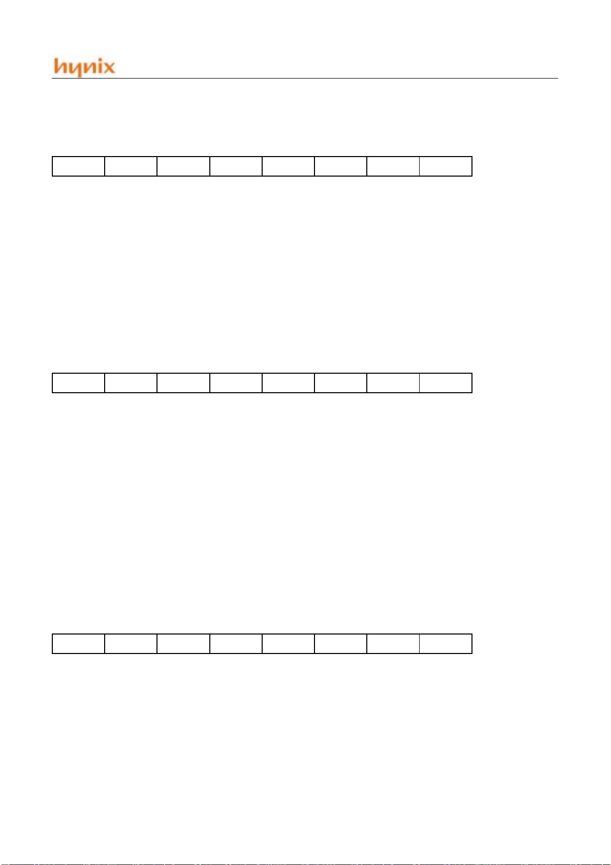
IP3: INTERRUPT PRIORITY REGISTER 3. : C1H
If the bit is 0, the corresponding interrupt has a lower priority and If the bit is 1, the corresponding interrupt has a higher priority.
- IPWDT IPADC IPIFC IPS2 IPS1 IPT4 IPT3
- IP3.7 Not implemented, reserved for future use.*
IPWDT IP3.6 Defines the Watchdog timer interrupt priority level.
IPADC IP3.5 Defines ADC interrupt priority level.
IPIFC IP3.4 Defines IF counter interrupt priority level.
IPS2 IP3.3 Defines SIO2 interrupt priority level.
IPS1 IP3.2 Defines SIO1 Interrupt priority level.
IPT4 IP3.1 Defines the Timer 4 interrupt priority level.
IPT3 IP3.0 Defines the Timer 3 interrupt priority level.
* User software should not write 1s to reserved bits. These bits may be used in future DTS3 products to invo ke new features. In that case,
the reset or inactive value of the new bit will be 0, and its active value will be 1.
REQUESTING TO SERVICE ONE OR MORE INTERRUPTS:
IR2: INTERRUPT REQUEST REGISTER 2. BIT ADDRESSABLE. : D8H
- - - IRX6 IRX5 IRX4 IRX3 IRX2
- IR2.7 Reserved for future use *
- IR2.6 Reserved for future use *
- IR2.5 Reserved for future use *
IRX6 IR2.4 External interrupt 6 flag. Set by hardware when External interrupt is detected. Cleared by hardware
when interrupt is processed.
IRX5 IR2.3 External interrupt 5 flag. Set by hardware when External interrupt is detected. Cleared by hardware
when interrupt is processed.
IRX4 IR2.2 External interrupt 4 flag. Set by hardware when External interrupt is detected. Cleared by hardware
when interrupt is processed.
IRX3 IR2.1 External interrupt 3 flag. Set by hardware when External interrupt is detected. Cleared by hardware
when interrupt is processed.
IRX2 IR2.0 External interrupt 2 flag. Set by hardware when External interrupt is detected. Cleared by hardware
when interrupt is processed.
* User software should not write 1s to reserved bits. These bits may be used in future DTS3 products to invo ke new features. In that case,
the reset or inactive value of the new bit will be 0, and its active value will be 1.
IR3: INTERRUPT REQUEST REGISTER 3. BIT ADDRESSABLE. : E8H
- IRWDT IRADC IRIFC IRS2 IRS1 IRT4 IRT3
- IR3.7 Reserved for future use *
IRWDT IR3.6 Watchdog timer overflow flag. Set by hardware when WDT overflows. Cleared by hardware as proces-
sor vectors to the interrupt service routine.
IRADC IR3.5 A/D conversion completio n flag. Set by hard ware when ADC completes. Cleared by hardware as pro-
cessor vectors to the interrupt service routine.
IRIFC IR3.4 IF counter interrupt flag. Set by hardware when run time of IF counter reaches to gate time. Cleared by
hardware as processor vectors to the interrupt service routine.
IRS2 IR3.3 SIO2 interrupt flag. Set by hardware when one TX/RX is completed. Cleared by hardware as processor
NOV., 2001 Ver 1.02 25

HMS91C8032/97C8032
vectors to the interrupt service routine.
IRS1 IR3.2 SIO1 interrupt flag. Set by hardware when one TX/RX is completed. Cleared by hardware when inter-
rupt is processed.
IRT4 IR3.1 Timer 4 Overflow flag. Set by hardware when the Timer/Counter 4 overflows. Cleared by hardware as
processor vectors to the interrupt service routine.
IRT3 IR3.0 Timer 3 Overflow flag. Set by hardware when the Timer/Counter 3 overflows. Cleared by hardware as
processor vectors to the interrupt service routine.
* User software should not write 1s to reserved bits. These bits may be used in future DTS3 products to invo ke new features. In that case,
the reset or inactive value of the new bit will be 0, and its active value will be 1.
IT2: EXTERNAL INTERRUPT TPYE REGISTER 2. BIT ADDRESSABLE. : D9H
IT5M1 IT5M0 IT4M1 IT4M0 IT3M1 IT3M0 IT2M1 IT2M0
IT5M1 IT2.7 See Table 4-4
IT5M0 IT2.6 See Table 4-4
IT4M1 IT2.5 See Table 4-4
IT4M0 IT2.4 See Table 4-4
IT3M1 IT2.3 See Table 4-4
IT3M0 IT2.2 See Table 4-4
IT2M1 IT2.1 See Table 4-4
IT2M0 IT2.0 See Table 4-4
ITxM[1:0] Select interrupt detect mode
0 0 Both rising & falling edge detection
0 1 Rising edge detect mode
1 0 Falling edge detect mode
1 1 Level (high) detect mode
Table 4-4 Interrupt Detect Mode
TCON: TIMER01/COUNTER01 CONTROL REGISTER. BIT ADDRESSABLE. : 88H
TF1 TR1 TF0 TR0 IE1 IT1 IE0 IT0
TF1 TCON.7 Timer 1 Overflow flag. Set by hardware when the Timer/Counter 1 overflows. Cleared by hardware as
processor vectors to the interrupt service routine.
TR1 TCON.6 Timer 1 run control bit. Set/cleared by software to turn Timer/Counter 1 ON/OFF.
TF0 TCON.5 Timer 0 Overflow flag. Set by hardware when the Timer/Counter 0 overflows. Cleared by hardware as
processor vectors to the interrupt service routine.
TR0 TCON.4 Timer 0 run control bit. Set/cleared by software to turn Timer/Counter 0 ON/OFF.
IE1 TCON.3 Interrupt 1 Edge flag. Set by hardware when external interrupt edge detected. Cleared when interrupt
processed.
IT1 TCON.2 Interrupt 1 Type control bit. Set/cleared by software to specify falling edge/low level triggered external
interrupts.
IE0 TCON.1 Interrupt 0 Edge flag. Set by hardware when external interrupt edge detected. Cleared when interrupt
processed.
IT0 TCON.0 Interrupt 0 Type control bit. Set/cleared by software to specify falling edge/low level triggered external
interrupts.
26 NOV., 2001 Ver 1.02
HMS91C8032/97C8032
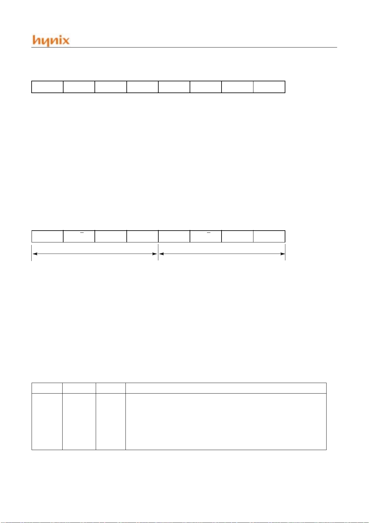
T34CON: TIMER34/COUNTER34 CONTROL REGISTER. BIT ADDRESSABLE. : 90H
TF4 TR4 TF3 TR3 T3_SUB T4_SUB
TF4 TCON.7 Timer 4 Overflow flag. Set by hardware when the Timer/Counter 4 overflows. Cleared by hardware as
processor vectors to the interrupt service routine.
TR4 TCON.6 Timer 4 run control bit. Set/cleared by software to turn Timer/Counter 4 ON/OFF.
TF3 TCON.5 Timer 3 Overflow flag. Set by hardware when the Timer/Counter 3 overflows. Cleared by hardware as
processor vectors to the interrupt service routine.
TR3 TCON.4 Timer 3 run control bit. Set/cleared by software to turn Timer/Counter 3 ON/OFF.
- TCON.3 Reserved for future use *
T3_SUB TCON.2 Switch main clock to sub clock for timer3 counting. This bit is a write-only register.
0 = Main Osc, 1 = Sub Osc.
- TCON.1 Reserved for future use *
T4_SUB TCON.0 Switch main clock to sub clock for timer4 counting. This bit is a write-only register.
0 = Main Osc, 1 = Sub Osc.
* User software should not write 1s to reserved bits. These bits may be used in future DTS3 products to invo ke new features. In that case,
the reset or inactive value of the new bit will be 0, and its active value will be 1.
TMOD: TIMER/COUNTER MODE CONTROL REGISTER. NOT BIT ADDRESSABLE. : 89H
GATE C /T M1 M0 GATE C/T M1 M0
Timer 1
GATE TMOD.7 When TRx (in TCON) is set and GATE = 1, TIMER/COUNTERx will run only while INTx pin is high
(hardware control). When GATE = 0, TIMER/COUNTERx will run only while TRx = 1 (software con-
trol).
C/T TMOD.6 Timer or Counter selector. Cleared for Timer operation (input from internal system clock). Set for
Counter operation (input from Tx input pin).
M1 TMOD.5 Mode selector bit. (See Table 4-5)
M0 TMOD.4 Mode selector bit. (See Table 4-5)
GATE TMOD.3 When TRx (in TCON) is set and GATE = 1, TIMER/COUNTERx will run only while INTx pin is high
(hardware control). When GATE = 0, TIMER/COUNTERx will run only while TRx = 1 (software con-
trol).
C/T TMOD.2 Timer or Counter selector. Cleared for Timer operation (input from internal system clock). Set for
Counter operation (input from Tx input pin).
M1 TMOD.1 Mode selector bit. (See Table 4-5)
M0 TMOD.0 Mode selector bit. (See Table 4-5)
M1 M0 Mode Operating Mode
0 0 0 13-bit Timer
0 1 1 16-bit Timer/Counter
1 0 2 8-bit Auto-Reload Timer/Counter
113
1 1 3 (Timer 1) Timer/Counter 1 stopped.
(Timer 0) TL0 is an 8-bit Timer/Counter controlled by the standard Timer 0
control bits, TH0 is an 8-bit Timer and is controlled by Timer 1 control bits.
Timer 0
Table 4-5 Timer 0 and Timer 1 Mode
NOV., 2001 Ver 1.02 27
 Loading...