HYNIX HMS91C7432 Datasheet

Hynix semiconductor
INTRODUCTION
From now on, you can hook your product onto the inter-net directly.
Put the PC aside, HMS91C7432 do all the jobs that the PC do for
inter-net connection.
HMS91C7432 is a CMOS IC with a complete TCP/IP protocol suite to facilitate
inter-net connection for embedded application. The built-in email engine can
transform any ASCII message to standard email format. It sends and receives
email; conduct the whole log on process automatically. Built-in PPP protocol
handle user-ISP handshaking and authentication process automatically. The
HMS91C7432 also includes the MODEM driver, no code should write to drive
the MODEM (parameter of modem must be transferred by the host to make
HMS91C7432 works with your modem).
Using HMS91C7432 is e asy, a simple 8 bit parallel p ort (8 bit data plus 4 control
lines) bridge the IC with your application. A serial DTE port is ready for directly
connect to an onboard modem or through DTE interface to a serial modem.
Make your product inter-net able, just add an HMS91C7432 on your BOM.
1

Hynix semiconductor
HMS91C7432 features and functions
z Implementation of the complete TCP/IP protocol suite
z Built-in Email sending and reception function.
z Standard SMTP protocol stack.
z Standard POP3 protocol stack.
z Standard PPP protocol stack to facilitate dial-up network log on.
z Standard DNS protocol stack, resolve URL with dynamic DNS server.
z Serial modem driver built-in.
z Support V.90 56Kflex modem or lower.
z 8 bit parallel interf ace to the user application.
z Serial DTE port for ease of modem interface.
z 5V or 3.3V operation voltage
z 20 pins SOP package
Detail description of HMS91C7432 function and its application
TCP/IP protocol suite is the key to inter-net
access. Email; Home Page materials and all
the data traffic on the inter-net are carry out
by using the TCP/IP well defined format.
Time before HMS91C7432 exist, most internet connection were to be handled by the PC.
Hand held devices and equipments must be
attached to the PC to get access to the
inter-net. Now the era of “PC-free” inter-net
connection has come. With HMS91C7432,
you can make your product be able to send
and receive email; surf on the WWW and
even “TALK” to another device through the
inter-net, by just plugging the telephone line
onto it.
The core of the HMS91C7432 is a complete
TCP/IP protocol suite. Files and messages
pass to the HMS91C7432 will be transformed
into the appropriate format and packets to
conform the inter-net standard. This
transformation is transparent to the user’s
application.
On top of the TCP/IP core, there is an Email
engine built-in. User’s program just needed
to inform the HMS91C7432 an email is going
to send and follow with the email body.
HMS91C7432 will then wake up the modem
and dial the ISP to log on the mail server. The
mail will be sent when log on has success.
HMS91C7432 complete this whole process
fully automatic.
the server, then it check and download any
email automatically. Each message will be
stored in the RAM buffer, HMS91C7432 will
notify the application program an email has
come and waiting for retrieve.
The built-in PPP module handles the “Log on
process”. This is a standard protocol to pass
the user’s account ID and the password to
the ISP. This module handles the
authentication and “Handshaking”. User’s
program just pass the user’s ID and
password to HMS91C7432 and the PPP do it
all.
HMS91C7432 (later version only) also equip
with a FTP module to facilitate file transfer
and file downloading from the FTP site. This
function is especially good for remote system
update and game download for hand-held
game inter-net access.
The standard serial DTE interface on the
HMS91C7432 ease the modem connection.
The built-in modem driver support V.90 and
56K flex dual modem or lower.
HMS91C7432 is controlled by an 8 bit
data/command port. This port accepts
command passed by the host MCU.
Incoming and outgoing mess age will be
passed between the host and the
HMS91C7432 through this port as well.
Reception of Email is as simple as getting
email on the PC. The application program
send a “Receive Email” command to the
HMS91C7432, it dial up the ISP and log on
2

Hynix semiconductor
Specifications of HMS91C7432
The HMS91C7432 TCP/IP communication controller is manufactured in advance CMOS
process.
The HMS91C7432 im plement complete TCP/I P protocol suite inc ludes PPP; IP; ICMP;T CP;
UDP; DNS; SMTP; POP3 protocol and additionally a general MODEM driver.
The HMS91C7432 is built-in with 96Kb SRAM (12K x 8) for communication and buffering, A full
duplex UART as DTE for ease of serial modem connection.
The HMS91C7432 has an 8 bits Data/Command port and 4 control pins to facilitate control and
communication between the Host MCU and the modem. There are only 20 simple commands,
each of which is a single byte long, to establish and to complete the whole internet
communication. 45 respond codes for the Host MCU to monitor the communication status.
Extremely low external component count. Very low power consumption.
Features :
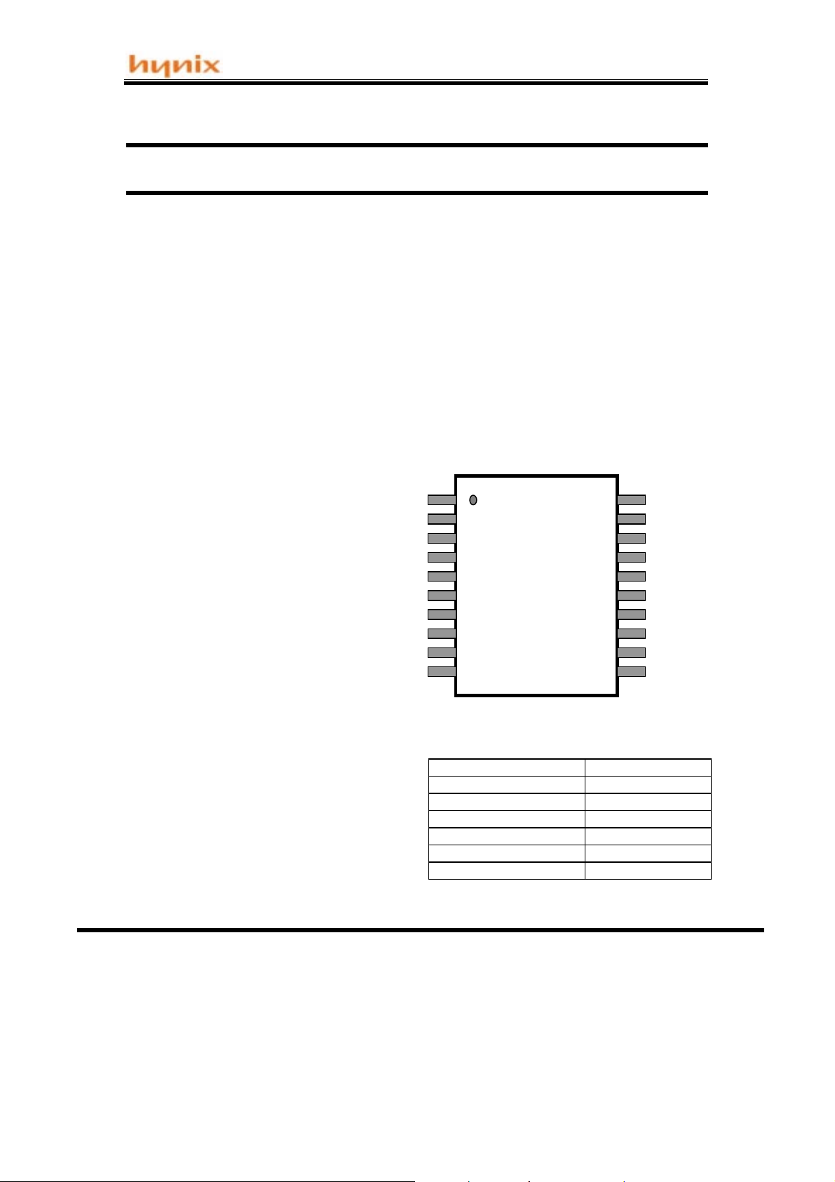
D0
D1
y
Implement TCP/IP protocol suit.
y
SMTP for sending email
y
POP3 for receiving email
y
PPP for dialup network log on
and hand shaking.
y
DNS protocol to resolve IP
address from URL
y
Full static operation
y
Full Duplex 56K/115Kbps UART
port for modem DTE connection.
y
Speed range up to 22.118MHz
y
8 bits Bi-directional Data/Command bus.
y
Modem driver included
y
Power control modes
9
Active mode
9
Power-down mode
y
Dissipating Current
ß
Active 25mA
ß
Power-down 10uA max.
y
20 single byte easy commands
y
45 respond codes
Package type 20-SOP
y
y
D2
D3
D4
D5
D6
D7
Test
VCC
20
2
3
HMS91C7432
4
5
6
7
8
9
10
Operating voltage 3.3V +/- 10%
Dissipating Current
Active mode 25 mA
Power down mode 10uA max.
Oscillation Frequency 11.0592 Mhz
Operating Temperature
Storage Temperature
SOP 20
19
18
17
16
15
14
13
12
11
-40 to +85
-65 to +150°C
RXD
TXD
Reset
Strobe
WR
INT
Wait
Xtal 2
Xtal 1
Vss
°C
3

Hynix semiconductor
Specifications of HMS91C7432
MNEMONIC PIN TYPE NAME AND FUNCTION
Vss 14
Vcc 9
D0 to D7 1 – 8 I/O
WAIT 14 Out
INT 15 Out
WR 16 In
STROBE 17 In
RXD 20 In
TXD 19 Out
RESET 13 In
TEST 10 In
XTAL 1 11 In
XTAL 2 12 Out
Ground :
Power Supply :
normal, and power-down operat io n.
Data/Command Port :
port with internal pull-ups . This port is for data transfer
between Host MCU, it also serves as command reception
and responds code iss uance port from and to the Host
MCU.
WAIT :
OK to start a cycle (assert a strobe), when high it
indicates that it is OK to end the cycle (de-assert a
strobe).
INT :
data/respond code are to be sent.
WRITE :
for a write cycle. Set this pin HIGH for a read cycle.
STROBE :
Data_Read or Data_Write operation is in process.
RXD :
TXD :
RESET :
oscillator is running resets the device.
TEST :
operation.
XTAL1 :
input to the internal clock generator circuits.
XTAL2 :
0V reference.
This is the power supply voltage for
This is an 8 bit bi-direc tional I/O
Handshake signal. W hen low it i ndicates that is
Active LOW Output a request to the Hos t MCU if
Active LOW write en ab le pin.
Data strobe signal.
UART serial input port.
UART serial output port.
A high level on this pin for 2us while the
Test pin, should be stuck at zero when norm al
Input to the inverting oscillator amplifier and
Output to the inverting oscillator amplifier.
Active low indicates a
Set this pin LOW
Table 1. Pin descript io ns
4

Hynix semiconductor
Specifications of HMS91C7432
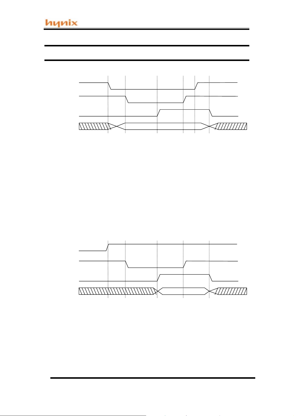
1 2 3 4 5 6
WR
Strobe
Wait
Data[7:0]
Figure 1. Data Write Cycle waveform
Data Write cycle phase transitions:
1. The Write line is asserted and the data is output to the parallel port
2. The data strobe is asserted, since WAIT is asserted low
3. The port waits for the acknowledge from the HMS91C7432 (WAIT de-asserted)
4. The data strobe is de-asserted
5. The write cycle ends
6. WAIT is asserted low to indicate that the next cycle may begin
Valid data
1 2 3 4 5
WR
Strobe
Wait
Data[7:0]
Figure 2. Data Read Cycle waveform
Data Read cycle phase transitions:
1. The Write line is set to HIGH to indicate read request
2. The data strobe is asserted, since WAIT is asserted low
3. The port waits for the acknowledge from the HMS91C7432 (WAIT de-asserted)
4. The data strobe is de-asserted after data is stored and the read cycle ends
5. WAIT is asserted low to indicate that the next cycle may begin
Valid data
5

Hynix semiconductor
µ
µ
µ
Specifications of HMS91C7432
❏
DC Characteristics
(Ta = -20 To +85 , Vcc = 5V 10%, Vss = 0V)
SYMBOL
V
IL
V
IL1
V
IH
V
IH1
V
IH2
V
OL
V
OH
I
IL
PARAMETER
Input low voltage,except Reset
Input low voltage,Reset
Input high voltage,except Xtal1,Reset
Input high voltage,Xtal1
Input high voltage, Reset
Output low voltage,D0~D7,Strobe,
WR,INT,Wait
Output high voltage, D0~D7,Strobe,
WR,INT,Wait
Logical 0 input current, D0~D7,Strobe,
WR,INT,Wait
I
OL
I
OH
V
IN
TEST
= 3.5mA
= -25µA
= 0.45V
LIMITS
MIN MAXCONDITIONS
-0.5
-0.5
0.7Vcc
0.7Vcc
0.6Vcc
0.75Vcc
-10
0.2Vcc-0.1
0.2Vcc+0.1
Vcc+0.5
Vcc+0.5VV
Vcc+0.5 V
1.0 V
-50
UNIT
V
V
V
A
I
TL
I
CC
Logical 1-to-0 input current,
D0~D7,Strobe,WR,INT,Wait
Power supply current :
Active mode@11.0592MHz
V
= 3.0V
IN
Vcc = 5V
-65
Power-down mode @11.0592MHz
NOTES :
1. See Figure 3 through 5 for Icc test conditions. Minimum Vcc for power down is 2V.
2. Under steady state (non-tra nsient) conditions,I
Maximum I
Maximum I
Maximum total I
If I
OL
per port : 10mA
OL
per 8-bit port D0~D7,Strobe,WR,INT,Wait : 15mA
OL
for all output pins : 71mA
OL
exceeds the test condition,VOL may exceed the related specification.Pins are not
must be externally limited as follows :
OL
guara nteed to sink current greater than the listed test conditions.
-650
16
10
A
mA
A
6

Hynix semiconductor
µ
µ
µ
Specifications of HMS91C7432
❏
DC Characteristics(Cont.)
(Ta = -20 To +85 , Vcc = 3.3V 10%, Vss = 0V)
SYMBOL
V
IL
V
IL1
V
IH
V
IH1
V
IH2
V
OL
V
OH
I
IL
PARAMETER
Input low voltage,except Reset
Input low voltage, Reset
Input high voltage,except Xtal1,Reset
Input high voltage,Xtal1
Input high voltage,Reset
Output low voltage,D0~D7,Strobe,
WR,INT,Wait
Output high voltage, D0~D7,Strobe,
WR,INT,Wait
Logical 0 input current, D0~D7,Strobe,
WR,INT,Wait
TEST
LIMITS
UNIT
MIN MAXCONDITIONS
-0.5
-0.5
0.7Vcc V
0.7Vcc V
0.6Vcc V
IOL= 1.6mA V
I
OH
V
IN
= -20µA
= 0.45V
2.7
-6
0.8
0.8
Vcc+0.3
Vcc+0.3
Vcc+0.3
0.45
-50
V
V
V
A
I
TL
I
CC
Logical 1-to-0 input current,
D0~D7,Strobe,WR,INT,Wait
Power supply current :
Active mode@11.0592
Power-down mode
= 2.0V
V
IN
Vcc = 3.3V
-40
-250
10
10
A
mA
A
7

Hynix semiconductor
Specifications of HMS91C7432
DC Characteristics(Cont.)
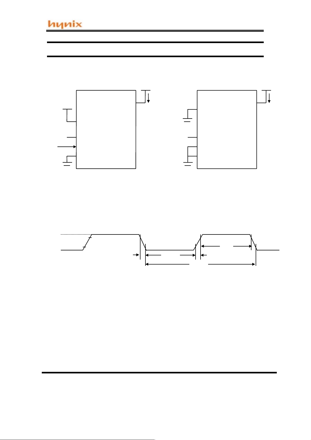
Vcc
Reset
(NC)
CLOCK
SIGNAL
All other pins are disconnected.
Figure 3. Icc Test Condition,Active Mode
Vcc-0.5
0. 5V
Xtal2
Xtal1
Vss
0.7Vcc
0.2Vcc-0.1
tCHCL
Vcc
Icc
Reset
(NC)
All other pins are disconnected.
Figure 4. Icc Test Condition,Power Down Mode
tCLCX tCLCH
Xtal2
Xtal1
Vss
tCHCX
Vcc
Icc
tCLCL
Figure 5. Clcok signal Wavefoerm for Icc Tests in Active Mode
tCLCH = tCHCL = 5ns
NOTES :
1. Icc(active mode) is meas ured with:
Xtal1 driven with tCLCH = tCHCL = 5ns, VIL = Vss + 0.5V, VIH = Vcc - 0.5V, X2 = N.C.
Reset = Vcc, all other pins are disconnected.
Icc would be slightly higher if a crystal oscillator is used (appr. 1mA)
2. Icc(power down mode) is measured with:
Xtal1 = Vss, Xtal2 = N.C., Reset = Vss, all other pins are disconnected.
8
 Loading...