


现货库存、技术资料、百科信息、热点资讯,精彩尽在鼎好!
p
Pulse-Width-Modulation Control Circuits TL494
CT
RT
GND
C1
SOP16/DIP16
(TOP VIEW)
1
2
3
4
5
6
7
8
16
15
14
13
12
11
10
NONINV
INPUT
INV INPUT
REF OUT
OUTPUT
CONTROL
Vcc
C2
E2
E1
9
Error
AMP 2
FEATURES
● Complete PWM Power Control Circuitry
● Uncommitted Outputs for 200 Ma Sink or Source Current
● Output Control Selects Single-Ended or Push-Pull Operation
● Internal Circuitry Prohibits Double Pulse at Either Output
● Variable Dead-Time Provides Control over Total Range
● Internal Regulator Provides a Stable 5-V Reference Supply,5%
● Circuit Architecture Allows Easy Synchronization
Error
AMP 1
NONINV
INPUT
INV INPUT
FEEDBACK
DEAD-TIME
CONTROL
DESCRIPTION
The TL494 incorporate on a single monolithic chip all the functions
required in the construction of a pulse-width-modulation control,
these devices offer the systems engineer the flexibility to tailor
the power supply control circuitry to his application.
The TL494 contains an error amplifier, an on-chip adjustable
oscillator, a dead-time control comparator, pulse-steering control
ORDERING INFORMATION
Device Package
TL494D 16 SOP
TL494N 18 DIP
flip-flop, a 5-volt, 5% precision regulator, and output-control circuit.
The error amplifier exhibits a common-mode voltage range from -0.3 volts to Vcc -2 volts. The dead-time control
comparator has a fixed offset that provides approximately 5% dead time when externally altered. The on-chip
oscillator may be bypassed by terminating R
(pin 6) to the reference output and providing a sawtooth in put to
T
CT (pin 5), or it may be used to drive the common circuits in synchronous multiple-rail power supplies. The
uncommited output transistors provide either common-emitter or emitter-follower output capability. Each Device
rovides for push-pull or single-ended output operation, which may be selected through the output-control funct
-ion. The architecture of these devices prohibits the possibility of either output being pulsed twice during push
-pull operation.
Functional Block Diagram
R
C
DEAD
TIME
CONTROL
NONINVERTING INPUT
INVERTING INPUT
NONINVERTING INPUT
INVERTING INPUT
Mar. 2006-Rev06
T
T
0.1V
ERROR AMPLIFIER
ERROR AMPLIFIER
OSCILLATOR
DEAD-TIME CONTROL COMPARATOR
+
1
-
+
2
-
PWM COMPARATOR
FEEDBACK
145
OUTPUT CONTROL
C1
PULSE-STEERING FLIP-FLOP
REFERENCE
Q1
Q2
C1
E1
C2
E2
Vcc
Vref
GND
HTC
Pulse-Width-Modulation Control Circuits TL494
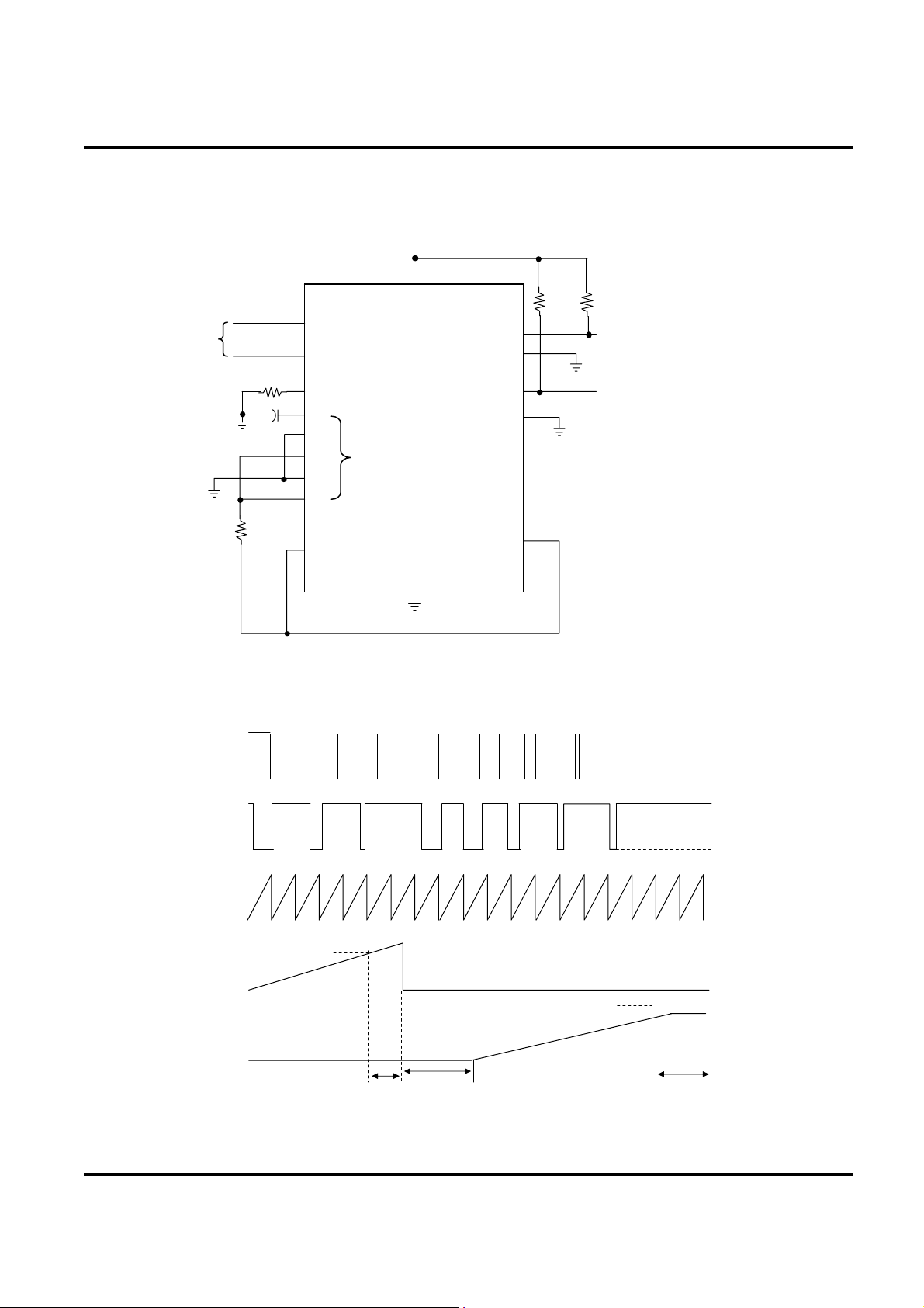
Parameter measurement information
Vcc = 15V
VOLTAGE
AT C1
TEST
INPUTS
50KΩ
12KΩ
0.01uF
DEAD-TIME
FEEDBACK
R
T
C
T
(+)
(-)
(+)
(-)
OUTPUT
CONTROL
ERROR
Vcc
GND
TEST CIRCUIT
C1
E1
C2
E2
REF OUT
150 Ω
2W
150 Ω
2W
OUTPUT 1
OUTPUT 2
Vcc
VOLTAGE
AT C2
VOLTAGE
AT C
DEAD-TIME
CONTROL
INPUT
FEEDBACK
DUTY
CIRCLE
Mar. 2006-Rev06
0
Vcc
0
T
THRESHOLD VOLTAGE
0 V
THRESHOLD VOLTAGE
0.7 V
0% MAX
0%
Figure 1. OPERATIONAL TEST CIRCUIT AND WAVEFORMS
HTC
146
 Loading...