

Page 1

Low Cost, Miniature Fiber
Optic Components with ST®,
SMA, SC and FC Ports
Technical Data
HFBR-0400 Series
Features
• Meets IEEE 802.3 Ethernet
and 802.5 Token Ring
Standards
• Low Cost Transmitters and
Receivers
• Choice of ST®, SMA, SC or
FC Ports
• 820 nm Wavelength
Technology
• Signal Rates up to 175
Megabaud
• Link Distances up to 4 km
• Specified with 50/125 µm,
62.5/125 µm, 100/140 µm,
and 200 µm HCS
• Repeatable ST Connections
within 0.2 dB Typical
• Unique Optical Port Design
for Efficient Coupling
• Auto-Insertable and Wave
Solderable
• No Board Mounting Hardware Required
• Wide Operating
Temperature Range
-40°C to 85°C
• AlGaAs Emitters 100%
Burn-In Ensures High
Reliability
• Conductive Port Option with
the SMA and ST Threaded
Port Styles
®
Fiber
Applications
• Local Area Networks
• Computer to Peripheral
Links
• Computer Monitor Links
• Digital Cross Connect Links
• Central Office Switch/PBX
Links
• Video Links
• Modems and Multiplexers
• Suitable for Tempest
Systems
• Industrial Control Links
Description
The HFBR-0400 Series of components is designed to provide cost
effective, high performance fiber
optic communication links for
information systems and
industrial applications with link
distances of up to 4 kilometers.
With the HFBR-24X6, the 125
MHz analog receiver, data rates
of up to 175 megabaud are
attainable.
Transmitters and receivers are
directly compatible with popular
“industry-standard” connectors:
ST, SMA, SC and FC. They are
completely specified with
multiple fiber sizes; including
50/125 µm, 62.5/125 µm, 100/
140 µm, and 200 µm.
Complete evaluation kits are
available for ST and SMA product
offerings; including transmitter,
receiver, connectored cable, and
technical literature. In addition,
ST and SMA connectored cables
are available for evaluation.
ST® is a registered trademark of AT&T.
HCS® is a registered trademark of the SpecTran Corporation.
46
5965-1655E (1/97)
Page 2
HFBR-0400 Series Part Number Guide
HFBR X4XXaa
1 = Transmitter Option T (Threaded Port Option)
2 = Receiver Option C (Conductive Port Receiver Option)
Option M (Metal Port Option)
4 = 820 nm Transmitter and Option K (Kinked Lead Option)
Receiver Products TA = Square pinout/straight lead
TB = Square pinout/bent leads
0 = SMA, Housed HA = Diamond pinout/straight leads
1 = ST, Housed HB = Diamond pinout/bent leads
2 = FC, Housed
E = SC, Housed 2 = Tx, Standard Power
3 = SMA Port, 90 deg. Bent Leads 4 = Tx, High Power
4 = ST Port, 90 deg. Bent Leads 2 = Rx, 5 MBd, TTL Output
5 = SMA Port, Straight Leads 6 = Rx, 125 MHz, Analog Output
6 = ST Port, Straight Leads
LINK SELECTION GUIDE
Data Rate (MBd) Distance (m) Transmitter Receiver Fiber Size (µm) Evaluation Kit
5 1500 HFBR-14X2 HFBR-24X2 200 HCS N/A
5 2000 HFBR-14X4 HFBR-24X2 62.5/125 HFBR-04X0
20 2700 HFBR-14X4 HFBR-24X6 62.5/125 HFBR-0414,
HFBR-0463
32 2200 HFBR-14X4 HFBR-24X6 62.5/125 HFBR-0414
55 1400 HFBR-14X4 HFBR-24X6 62.5/125 HFBR-0414
125 700 HFBR-14X4 HFBR-24X6 62.5/125 HFBR-0416
155 600 HFBR-14X4 HFBR-24X6 62.5/125 HFBR-0416
175 500 HFBR-14X4 HFBR-24X6 62.5/125 HFBR-0416
For additional information on specific links see the following individual link descriptions. Distances measured over temperature range
from 0 to 70°C.
Applications Support Guide
This section gives the designer
information necessary to use the
HFBR-0400 series components to
make a functional fiber-optic
transceiver. HP offers a wide
selection of evaluation kits for
hands-on experience with fiberoptic products as well as a wide
range of application notes complete with circuit diagrams and
board layouts. Furthermore, HP’s
application support group is
always ready to assist with any
design consideration.
Application Literature
Title Description
HFBR-0400 Series Transmitter & Receiver Reliability Data
Reliability Data
Application Bulletin 73 Low Cost Fiber Optic Transmitter & Receiver Interface Circuits
Application Bulletin 78 Low Cost Fiber Optic Links for Digital Applications up to 155 MBd
Application Note 1038 Complete Fiber Solutions for IEEE 802.3 FOIRL, 10Base-FB and 10 Base-FL
Application Note 1065 Complete Solutions for IEEE 802.5J Fiber-Optic Token Ring
Application Note 1073 HFBR-0319 Test Fixture for 1X9 Fiber Optic Transceivers
Application Note 1086 Optical Fiber Interconnections in Telecommunication Products
47
Page 3

HFBR-0400 Series Evaluation Kits
HFBR-0410 ST Evaluation Kit
Contains the following :
• One HFBR-1412 transmitter
• One HFBR-2412 five megabaud
TTL receiver
• Three meters of ST connectored 62.5/125 (µm fiber optic
cable with low cost plastic
ferrules.
• Related literature
HFBR-0414 ST Evaluation Kit
Includes additional components
to interface to the transmitter and
receiver as well as the PCB to
reduce design time.
Contains the following:
• One HFBR-1414T transmitter
• One HFBR-2416T receiver
• Three meters of ST connectored 62.5/125 µm fiber optic
cable
• Printed circuit board
• ML-4622 CP Data Quantizer
• 74ACTllOOON LED Driver
• LT1016CN8 Comparator
• 4.7 µH Inductor
• Related literature
HFBR-0400 SMA Evaluation Kit
Contains the following :
• One HFBR-1402 transmitter
• One HFBR-2402 five megabaud
TTL receiver
• Two meters of SMA
connectored 1000 µm plastic
optical fiber
• Related literature
HFBR-0416 Evaluation Kit
Contains the following:
• One fully assembled 1x9
transceiver board for 155 MBd
evaluation including:
-HFBR-1414 transmitter
-HFBR-2416 receiver
-circuitry
• Related literature
HFBR-0463 Ethernet MAU Evaluation Kit
Contains the following:
• One fully assembled Media
Attachment Unit (MAU) board
which includes:
-HFBR-1414 transmitter
-HFBR-2416 receiver
-HFBR-4663 IC
• Related literature
Note: Cable not included. Order
HFBR-BXS010 seperately (2
pieces)
Package and Handling Information
Package Information
All HFBR-0400 Series
transmitters and receivers are
housed in a low-cost, dual-inline
package that is made of high
strength, heat resistant, chemically resistant, and UL 94V-O
flame retardant ULTEM® (plastic
(UL File #E121562). The
transmitters are easily identified
by the light grey color connector
port. The receivers are easily
identified by the dark grey color
connector port. (Black color for
conductive port.) The package is
designed for auto-insertion and
wave soldering so it is ideal for
high volume production
applications.
Handling and Design Information
Each part comes with a protective
port cap or plug covering the
optics. These caps/plugs will vary
by port style. When soldering, it
is advisable to leave the protective cap on the unit to keep the
optics clean. Good system
performance requires clean port
optics and cable ferrules to avoid
obstructing the optical path.
Clean compressed air often is
sufficient to remove particles of
dirt; methanol on a cotton swab
also works well.
Recommended Chemicals for Cleaning/Degreasing HFBR-0400 Products
Alcohols: methyl, isopropyl,
isobutyl. Aliphatics: hexane,
heptane, Other: soap solution,
naphtha.
Do not use partially halogenated
hydrocarbons such as 1,1.1
trichloroethane, ketones such as
MEK, acetone, chloroform, ethyl
acetate, methylene dichloride,
phenol, methylene chloride, or
N-methylpyrolldone. Also, HP
does not recommend the use of
cleaners that use halogenated
hydrocarbons because of their
potential environmental harm.
Ultem® is a registered Trademark of the GE corporation.
48
Page 4
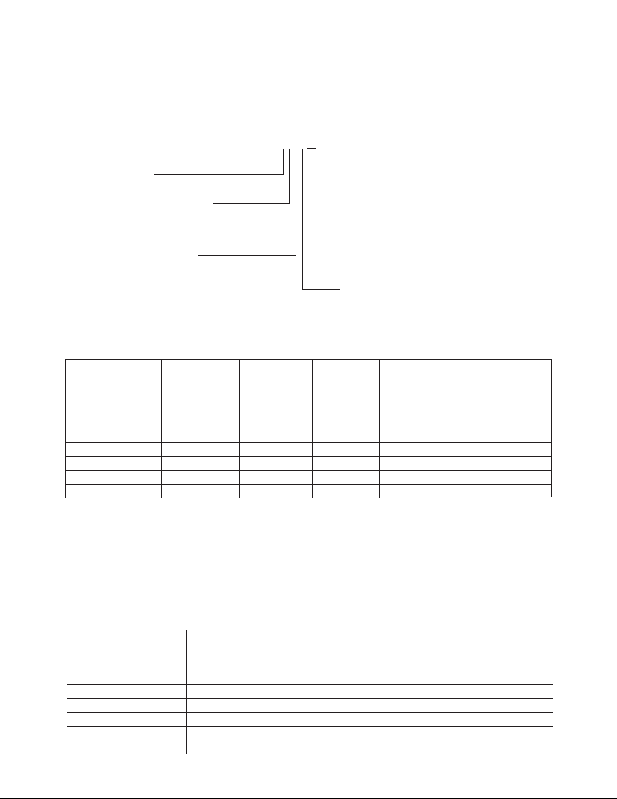
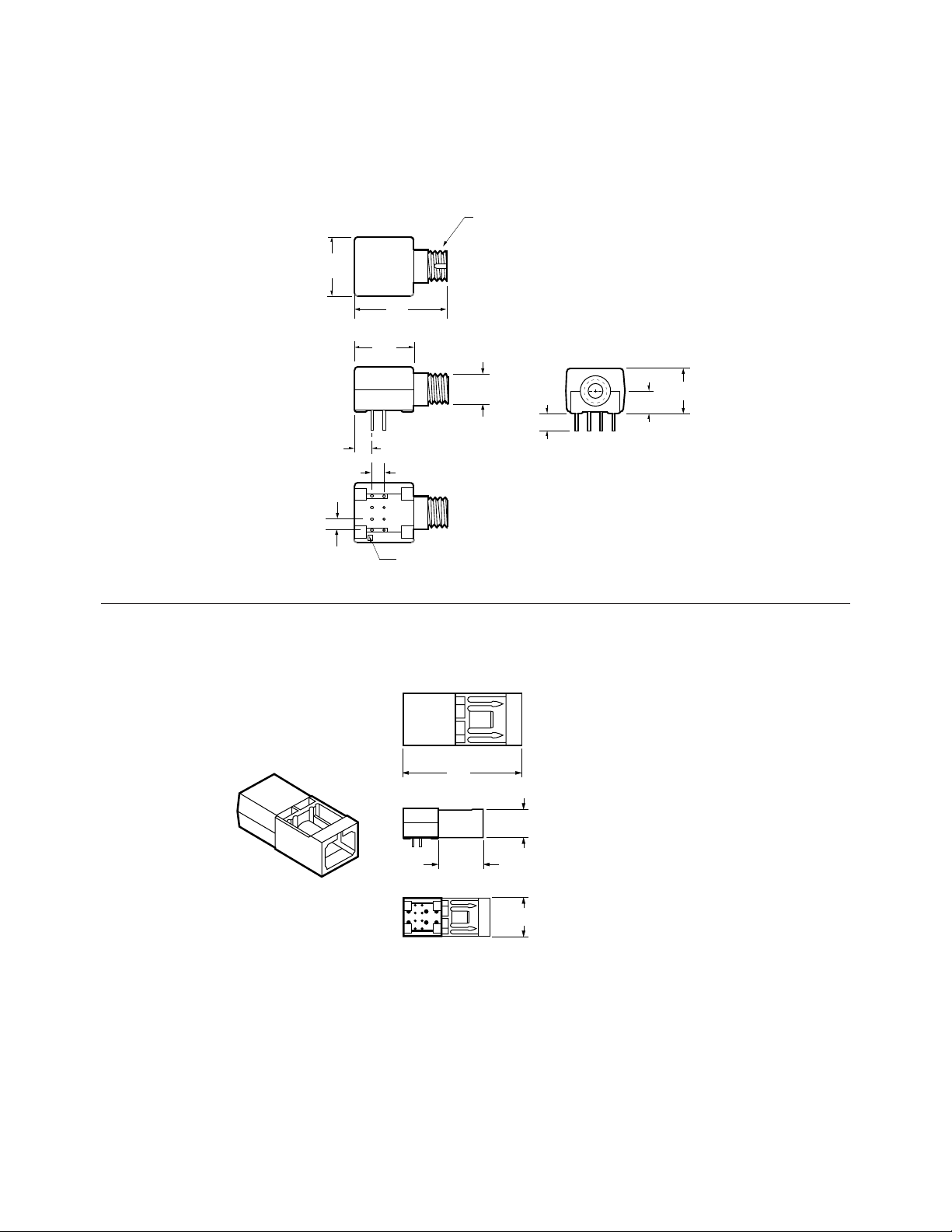
Mechanical Dimensions HFBR-0400 SMA Series
HFBR-X40X
12.7
(0.50)
Rx/Tx
ORIGIN
hp YYWW
COUNTRY OF
12.7
(0.50)
HFBR-X40X
22.2
(0.87)
1/4 - 36 UNS 2A THREAD
6.35
(0.25)
HFBR-X43X
8.6
(0.34)
DIA
PINS 1,4,5,8
0.51 X 0.38
(0.020 X 0.015)
PINS 2,3,6,7
0.46
(0.018)
2.5
(0.10)
12
34
3.81
(0.15)
DIA.
DIA PIN
CIRCLE
7.1
(0.28)
2.54
(0.10)
524
3
6
7
8
1
PIN NO. 1
INDICATOR
PART MARKING
4.8
TYP
(0.19)
2.3
TYP
(0.09)
YY WW
(0.25)
13.0
(0.51)
6.4
DIA
7.1
(0.28)
DIA
3.6
(0.14)
1.27
(0.05)
2.54
(0.10)
5.1
(0.20)
10.2
(0.40)
HFBR-X45X
3.6
MIN
(0.14)
NOTE 2
DIA
(0.34)
NOTE 2
NOTE: ALL DIMENSIONS IN MILLIMETRES AND (INCHES).
12
34
0.46
(0.018)
2.5
(0.10)
2.5
(0.10)
(0.28)
.46
(0.018)
7.1
TYP
DIA PIN
CIRCLE
DIA
DIA
TYP
2.5
(0.10)
3.0
(0.12)
9.1
(0.36)
TYP
TYP
13.2
(052)
PART MARKING
YY WW
13.0
(0.51)
2.0
(0.08)
4.1
(0.16)
7.1
(0.28)
(0.08)
(0.16)
2.0
4.1
DIA
1/4 - 36 UNS 2A
THREAD8.6
1/4 - 36 UNS 2A
THREAD
49
Page 5
Mechanical Dimensions HFBR-0400 ST Series
HFBR-X41X
12.7
(0.50)
Rx/Tx
ORIGIN
hp YYWW
COUNTRY OF
12.7
(0.50)
HFBR-X41X
27.2
(1.07)
8.2
(0.32)
6.35
(0.25)
HFBR-X44X
3.6
(0.14)
8.6
(0.34)
MIN
NOTE 2
(0.10)
2.5
DIA
(0.020 X 0.015)
PINS 2,3,6,7
(0.018)
TYP
PINS 1,4,5,8
0.51 X 0.38
0.46
DIA
2.5
(0.10)
12
34
3.81
(0.15)
DIA PIN
CIRCLE
7.1
(0.28)
0.46 (0.018)
PIN DIA
2.54
(0.10)
5
4
6
2
7
8
13
PIN NO. 1
INDICATOR
4.9
TYP
(0.19)
2.4
TYP
(0.09)
3.0
TYP
(0.12)
2.5
TYP
(0.10)
X-YWW
(0.73)
(0.28)
2.0
(0.08)
7.0
DIA
(0.28)
18.6
7.1
DIA
PART MARKING
7.0
(0.28)
3.6
(0.14)
DIA
8.2
8.2
(0.32)
1.27
(0.05)
2.54
(0.10)
5.1
(0.20)
10.2
(0.40)
HFBR-X46X
50
8.6
(0.34)
NOTE 2
DIA
21
34
2.5 (0.10)
DIA PIN
CIRCLE
0.46
(0.018)
7.1
(0.28)
PIN DIA
18.6
(0.73)
13.2
(0.52)
9.1
(0.36)
NOTE: ALL DIMENSIONS IN MILLIMETRES AND (INCHES).
X-YWW
2.O
(0.08)
7.1
DIA
(0.28)
PART MARKING
7.0
(0.28)
DIA
8.2
(0.32)
Page 6
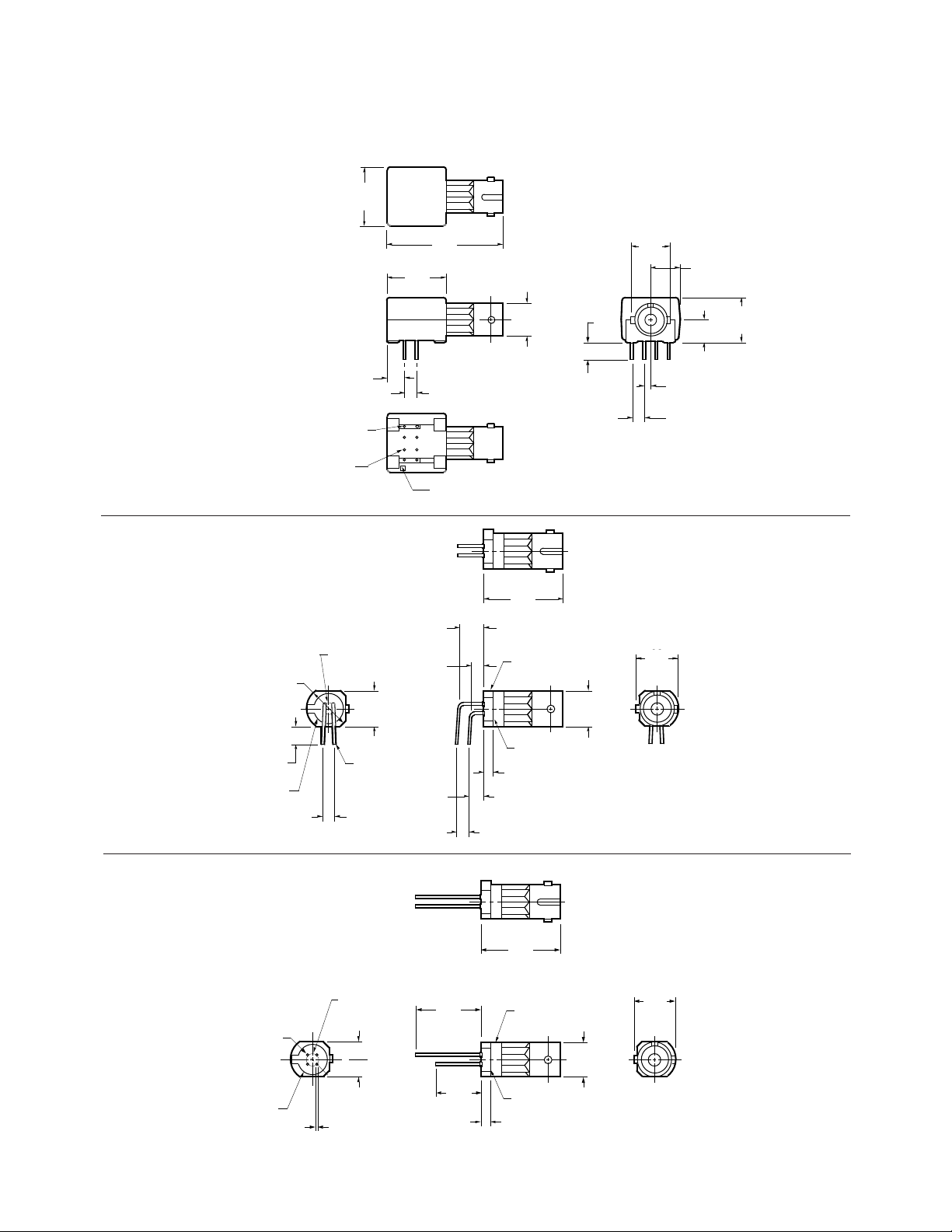
Mechanical Dimensions HFBR-0400T Threaded ST Series
HFBR-X41XT
12.7
(0.50)
Rx/Tx
ORIGIN
hp YYWW
COUNTRY OF
12.7
(0.50)
5.1
(0.20)
HFBR-X41XT
27.2
(1.07)
8.4
(0.33)
7.6
(0.30)
6.35
(0.25)
HFBR-X44XT
HFBR-X46XT
8.6
(0.34)
3.6
(0.14)
NOTE 2
MIN
DIA
(0.020 X 0.015)
PINS 2,3,6,7
(0.018)
2.5
(0.10)
12
34
3.81
(0.15)
PINS 1,4,5,8
0.51 X 0.38
0.46
DIA
DIA PIN
CIRCLE
7.1
(0.28)
0.46 (0.018)
PIN DIA
2.5
TYP
(0.10)
(0.19)
(0.09)
3.0
(0.12)
2.5
(0.10)
4.9
2.4
2.54
(0.10)
5
3
6
24
7
8
1
PIN NO. 1
INDICATOR
TYP
TYP
TYP
TYP
DIA.
YY WW
7.1
(0.28)
3/8 - 32 UNEF - 2A
5.1
(0.20)
18.5
(0.73)
PART MARKING
7.1
DIA
(0.28)
2.0
(0.08)
4.1
(0.16)
5.1
(0.20)
DIA
7.6
(0.30)
ACROSS THREAD
FLATS
3/8 - 32 UNEF - 2A
THREAD
3.6
(0.14)
8.4
(0.33)
1.27
(0.05)
2.54
(0.10)
5.1
(0.20)
10.2
(0.40)
8.6
(0.34)
NOTE 2
DIA
2.5
(0.10)
12
34
DIA PIN
CIRCLE
(0.28)
0.46
(0.018)
7.1
PIN DIA
9.1
(0.36)
13.2
(0.52)
(0.08)
(0.16)
18.5
(0.73)
8.4
(0.33)
PART MARKING
YY WW
2.0
4.1
7.6
(0.30)
ACROSS THREAD
FLATS
3/8 - 32 UNEF - 2A
THREAD
51
Page 7
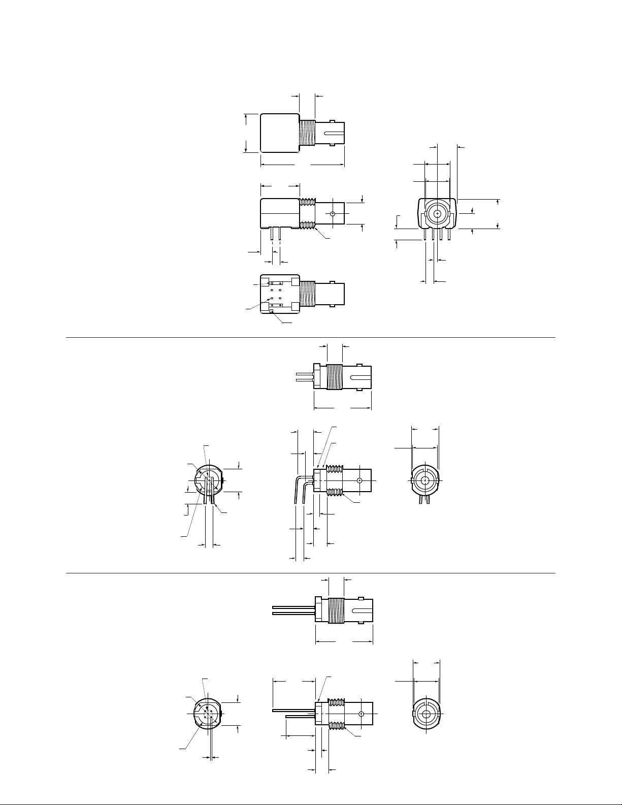
Mechanical Dimensions HFBR-0400 FC Series
12.7
(0.50)
Rx/Tx
ORIGIN
hp YYWW
COUNTRY OF
19.6
(0.77)
12.7
(0.50)
HFBR-X42X
M8 x 0.75 6G
THREAD (METRIC)
Mechanical Dimensions HFBR-0400 SC Series
HFBR-X4EX
3.81
(0.15)
2.5
(0.10)
2.5
(0.10)
5
3
6
24
7
8
1
PIN NO. 1
INDICATOR
Rx/Tx
COUNTRY OF
ORIGIN
hp YYWW
(1.128)
7.9
(0.31)
HFBR-X4EX
28.65
10.0
(0.394)
3.6
(0.14)
5.1
(0.20)
10.2
(0.40)
52
15.95
(0.628)
12.7
(0.500)
Page 8
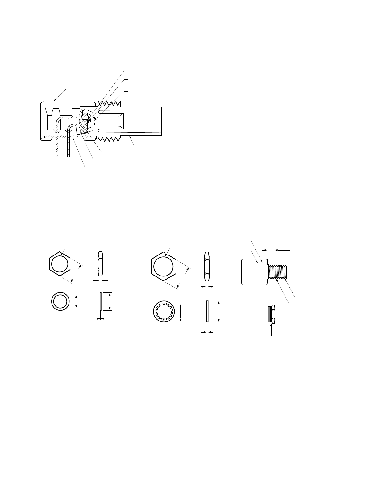
LED OR DETECTOR IC
LENS–SPHERE
HOUSING
HEADER
EPOXY BACKFILL
PORT GROUNDING PATH INSERT
(ON TRANSMITTERS ONLY)
LENS–WINDOW
CONNECTOR PORT
Figure 1. HFBR-0400 ST Series Cross-Sectional View.
Panel Mount Hardware
HFBR-4401: for SMA Ports HFBR-4411: for ST Ports
1/4 – 36 UNEF –
2B THREAD
3/8 – 32 UNEF2B THREAD
PART NUMBER
DATE CODE
0.2 IN.
7,87
HEX-NUT
WASHER
(0.310)
6.61
(0.260)
DIA
(0.065)
7.87
(0.310)
(0.005)
1.65
0.14
TYP
DIA
HEX-NUT
WASHER
12.70
(0.50)
10.41
(0.410)
DIA
MAX
DIA
(0.065)
14.27
(0.563)
0.46
(0.018)
1.65
(Each HFBR-4401 and HFBR-4411 kit consists of 100 nuts and 100 washers.)
Port Cap Hardware
HFBR-4402: 500 SMA Port Caps
HFBR-4120: 500 ST Port Plugs (120 psi)
HFBR-4412: 500 FC Port Caps
HFBR-4417: 500 SC Port Plugs
TYP
DIA
Rx/Tx
ORIGIN
hp YYWW
COUNTRY OF
WALL
HFBR-X40X
3/8 - 32 UNEF - 2A THREADING
1 THREAD AVAILABLE
NUT
WASHER
53
Page 9
Options
In addition to the various port
styles available for the HFBR0400 series products, there are
also several extra options that
can be ordered. To order an
option, simply place the corresponding option number at the
end of the part number. For
instance, a metal-port option SMA
receiver would be HFBR-2406M.
You can add any number of
options in series at the end of a
part number. Please contact your
local sales office for further
information or browse HP’s fiber
optics home page at http://
www.hp.com/go/fiber
Option T (Threaded Port
Option)
• Allows ST style port components to be panel mounted.
• Compatible with all current
makes of ST multimode
connectors
• Mechanical dimensions are
compliant with MIL-STD83522/13
• Maximum wall thickness when
using nuts and washers from
the HFBR-4411 hardware kit is
2.8 mm (0.11 inch)
• Available on all ST ports
Option C (Conductive Port Receiver Option)
• Designed to withstand electrostatic discharge (ESD) of 25kV
to the port
• Significantly reduces effect of
electromagnetic interference
(EMI) on receiver sensitivity
• Allows designer to separate the
signal and conductive port
grounds
• Recommended for use in noisy
environments
• Available on SMA and threaded
ST port style receivers only
Option M (Metal Port Option)
• Nickel plated aluminum connector receptacle
• Designed to withstand electrostatic discharge (ESD) of 15kV
to the port
• Significantly reduces effect of
electromagnetic interference
(EMI) on receiver sensitivity
• Allows designer to separate the
signal and metal port grounds
• Recommended for use in very
noisy environments
• Available on SMA, FC, ST, and
threaded ST ports
Option K (Kinked Lead Option)
• Grounded outside 4 leads are
“kinked”
• Allows components to stay
anchored in the PCB during
wave solder and aqueous wash
processes
Options TA, TB, HA, HB (Active Device Mount Options)
(These options are unrelated to
the threaded port option T.)
• All metal, panel mountable
package with a 3 or 4 pin
receptacle end
• Available for HFBR-14X4, 24X2
and 24X6 components
• Choose from diamond or
square pinout, straight or bent
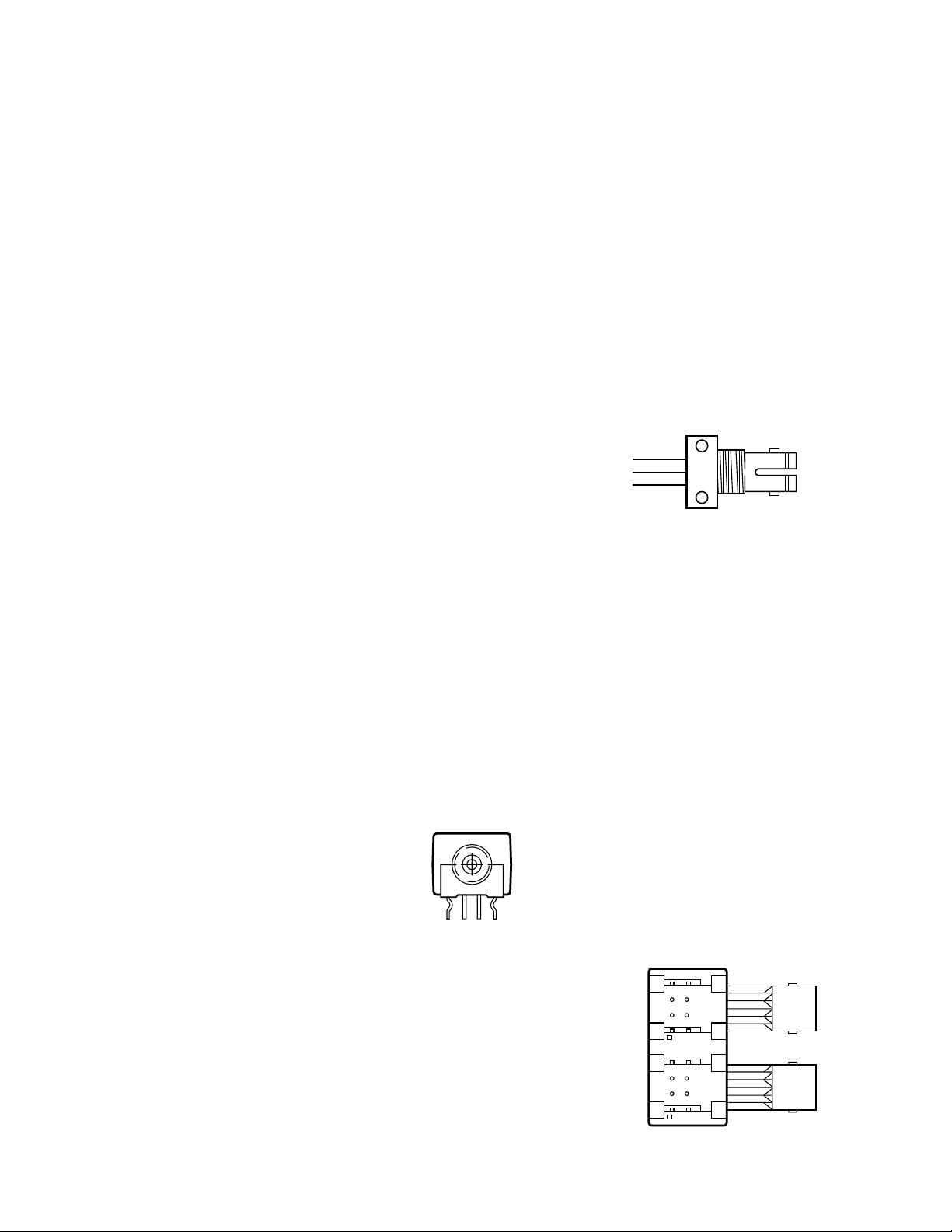
leads ADM Picture
• TA = Square pinout/straight
leads
TB = Square pinout/bent leads
HA = Diamond pinout/straight
leads
HB = Diamond pinout/bent
leads
Duplex Option
In addition to the standard
options, some HFBR-0400 series
products come in a duplex configuration with the transmitter on
the left and the receiver on the
right. This option was designed
for ergonomic and efficient
manufacturing. The following
part numbers are available in the
duplex option:
HFBR-5414 (Duplex ST)
HFBR-5414T (Duplex Threaded
ST)
HFBR-54E4 (Duplex SC)
45
36
27
54
18
45
36
27
18
Page 10

Typical Link Data
HFBR-0400 Series
Description
The following technical data is
taken from 4 popular links using
the HFBR-0400 series: the 5 MBd
link, Ethernet 20 MBd link,
Token Ring 32 MBd link, and the
155 MBd link. The data given
corresponds to transceiver solutions combining the HFBR-0400
series components and various
recommended transceiver design
circuits using off-the-shelf
electrical components. This data
is meant to be regarded as an
example of typical link performance for a given design and does
not call out any link limitations.
Please refer to the appropriate
application note given for each
link to obtain more information.
5 MBd Link (HFBR-14XX/24X2)
Link Performance -40°C to +85°C unless otherwise specified
Parameter Symbol Min. Typ. Max. Units Conditions Reference
Optical Power Budget OPB
50
with 50/125 µm fiber NA = 0.2
Optical Power Budget OPB
62.5
with 62.5/125 µm fiber NA = 0.27
Optical Power Budget OPB
100
with 100/140 µm fiber NA = 0.30
Optical Power Budget OPB
200
with 200 µm fiber NA = 0.37
Date Rate Synchronous dc 5 MBd Note 2
Asynchronous dc 2.5 MBd Note 3,
Propagation Delay t
PLH
LOW to HIGH PR = -21 dBm Peak
Propagation Delay t
PHL
HIGH to LOW
System Pulse Width t
PLH-tPHL
Distortion length = 1 m
Bit Error Rate BER 10
4.2 9.6 dB HFBR-14X4/24X2 Note 1
8.0 15 dB HFBR-14X4/24X2 Note 1
8.0 15 dB HFBR-14X2/24X2 Note 1
12 20 dB HFBR-14X2/24X2 Note 1
Fig. 7
72 ns TA = 25°C, Figs. 6, 7, 8
46 ns
26 ns Fiber cable
-9
Data Rate <5 Bd
PR > -24 dBm Peak
Notes:
1. OPB at TA = -40 to 85°C, VCC = 5.0 V dc, I
2. Synchronous data rate limit is based on these assumptions: a) 50% duty factor modulation, e.g., Manchester I or BiPhase
Manchester II; b) continuous data; c) PLL Phase Lock Loop demodulation; d) TTL threshold.
3. Asynchronous data rate limit is based on these assumptions: a) NRZ data; b) arbitrary timing-no duty factor restriction; c) TTL
threshold.
= 60 mA. PR = -24 dBm peak.
F ON
55
Page 11
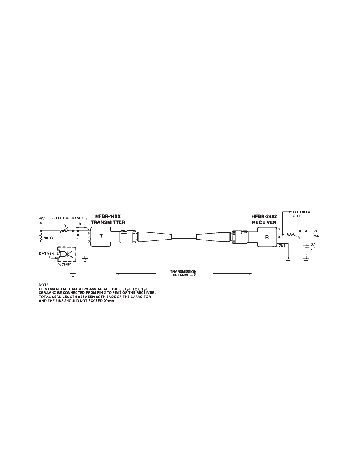
5 MBd Logic Link Design
If resistor R1 in Figure 2 is
70.4 Ω, a forward current IF of
48 mA is applied to the HFBR14X4 LED transmitter. With IF =
48 mA the HFBR-14X4/24X2
logic link is guaranteed to work
with 62.5/125 µm fiber optic
cable over the entire range of 0
to 1750 meters at a data rate of
dc to 5 MBd, with arbitrary data
format and pulse width distortion
typically less than 25%. By
setting R1 = 115 Ω, the transmitter can be driven with IF= 30 mA,
if it is desired to economize on
power or achieve lower pulse
distortion.
The following example will illustrate the technique for selecting
the appropriate value of IF and R1.
Maximum distance required
= 400 meters. From Figure 3 the
drive current should be 15 mA.
From the transmitter data
VF= 1.5 V (max.) at IF = 15 mA
as shown in Figure 9.
VCC - VF5 V - 1.5 V
R1 = ––––––– = –––––––––
I
F
15 mA
R1 = 233␣ Ω
The curves in Figures 3, 4, and 5
are constructed assuming no inline splice or any additional
system loss. Should the link
consists of any in-line splices,
these curves can still be used to
calculate link limits provided they
are shifted by the additional
system loss expressed in dB. For
example, Figure 3 indicates that
with 48 mA of transmitter drive
current, a 1.75 km link distance
is achievable with 62.5/125 µm
fiber which has a maximum
attenuation of 4 dB/km. With
2 dB of additional system loss, a
1.25 km link distance is still
achievable.
Figure 2. Typical Circuit Configuration.
56
Page 12

0
60
Figure 3. HFBR-1414/HFBR-2412
Link Design Limits with 62.5/125 µm
Cable.
75
70
65
60
55
50
45
40
PROPOGATION DELAY –ns
35
PHL
30
OR t
25
PHL
t
20
-22 -21 -20 -19 -18 -17 -16 -15 -14 -13 -12
t
(TYP) @ 25°C
PLH
t
(TYP) @ 25°C
PHL
PR – RECEIVER POWER – dBm
Figure 4. HFBR-14X2/HFBR-24X2
Link Design Limits with 100/140 µm
Cable.
55
50
45
40
35
30
D – NRZ DISTORTION – ns
t
25
20
-22 -21 -20 -19 -18 -17 -16 -15 -14 -13 -12
PR – RECEIVER POWER – dBm
-1
-2
-3
-4
-5
-6
0 0.4 0.8 1.2 1.6 2
10 LOG (t/to) NORMALIZED TRANSMITTER CURRENT (dB)
WORST CASE
-40°C, +85°C
UNDERDRIVE
CABLE ATTENUATION dB/km
α MAX (-40°C, +85°C) 4
α MIN (-40°C, +85°C) 1
α TYP (-40°C, +85°C) 2.8
LINK LENGTH (km)
TYPICAL 26°C
UNDERDRIVE
Figure 5. HFBR-14X4/HFBR-24X2
Link Design Limits with 50/125 µm
Cable.
50
40
30
20
TRANSMITTER FORWARD CURRENT (mA)
F
I
Figure 6. Propagation Delay through
System with One Meter of Cable.
Figure 7. Typical Distortion of Pseudo
Random Data at 5 Mb/s.
Figure 8. System Propagation Delay Test Circuit and Waveform Timing Definitions.
57
Page 13

Ethernet 20 MBd Link (HFBR-14X4/24X6)
(refer to Application Note 1038 for details)
Typical Link Performance
Parameter Symbol Typ.
[1,2]
Units Conditions
Receiver Sensitivity -34.4 dBm 20 MBd D2D2 Hexadecimal Data
average 2 km 62.5/125 µm fiber
Link Jitter 7.56 ns pk-pk ECL Out Receiver
7.03 ns pk-pk TTL Out Receiver
Transmitter Jitter 0.763 ns pk-pk 20 MBd D2D2 Hexadecimal Data
Optical Power P
LED rise time t
LED fall time t
T
r
f
-15.2 dBm 20 MBd D2D2 Hexadecimal Data
average Peak I
F,ON
= 60 mA
1.30 ns 1 MHz Square Wave Input
3.08 ns
Mean difference |tr-tf| 1.77 ns
Bit Error Rate BER 10
-10
Output Eye Opening 36.7 ns At AUI Receiver Output
Data Format 50% Duty Factor 20 MBd
Notes:
1. Typical data at TA = 25°C, VCC = 5.0 V dc.
2. Typical performance of circuits shown in Figure 1 and Figure 3 of AN-1038 (see applications support section).
Token Ring 32 MBd Link (HFBR-14X4/24X6)
(refer to Application Note 1065 for details)
Typical Link Performance
Parameter Symbol Typ.
[1,2]
Units Conditions
Receiver Sensitivity -34.1 dBm 32 MBd D2D2 Hexadecimal Data
average 2 km 62.5/125 µm fiber
Link Jitter 6.91 ns pk-pk ECL Out Receiver
5.52 ns pk-pk TTL Out Receiver
Transmitter Jitter 0.823 ns pk-pk 32 MBd D2D2 Hexadecimal Data
Optical Power Logic Level “0” P
Optical Power Logic Level “1” P
T OFF
LED Rise Time t
LED Fall Time t
T ON
r
f
-12.2 dBm peak Transmitter TTL in I
I
= 1 mA
-82.2
F OFF
F ON
1.3 nsec 1 MHz Square Wave Input
3.08 nsec
= 60 mA,
Mean Difference |tr-tf| 1.77 nsec
Bit Error Rate BER 10
-10
Data Format 50% Duty Factor 32 MBd
Notes:
1. Typical data at TA = 25°C, VCC = 5.0 V dc.
2. Typical performance of circuits shown in Figure 1 and Figure 3 of AN-1065 (see applications support section)
58
Page 14

155 MBd Link (HFBR-14X4/24X6)
(refer to Application Bulletin 78 for details)
Typical Link Performance
Parameter Symbol Typ.
Optical Power Budget OPB
50
with 50/125 µm fiber
Optical Power Budget OPB
62
with 62.5/125 µm fiber
Optical Power Budget OPB
100
with 100/140 µm fiber
Optical Power Budget OPB
200
with 200 µm HCSfFiber
Data Format 20% to 1 175 MBd
80% Duty Factor
System Pulse Width |t
PLH-tPHL
| 1 ns PR = -7 dBm Peak
Distortion 1 meter 62.5/125 µm fiber
Bit Error Rate BER 10
Notes:
1. Typical data at TA = 25°C, VCC = 5.0 V dc, PECL serial interface.
2. Typical OPB was determined at a probability of error (BER) of 10-9. Lower probabilities of error can be achieved with short fibers
that have less optical loss.
[1,2]
Units Max. Units Conditions Ref.
7.9 13.9 dB NA = 0.2 Note 2
11.7 17.7 dB NA = 0.27
11.7 17.7 dB NA = 0.30
16.0 22.0 dB NA = 0.35
-9
Data Rate < 100 MBaud
PR >-31 dBm Peak Note 2
59
Page 15

HFBR-14X2/14X4 LowCost High-Speed
Transmitters
Description
The HFBR-14XX fiber optic
transmitter contains an 820 nm
AlGaAs emitter capable of
efficiently launching optical
power into four different optical
fiber sizes: 50/125 µm, 62.5/125
µm, 100/140 µm, and 200 µm
HCS®. This allows the designer
flexibility in choosing the fiber
size. The HFBR-14XX is designed
to operate with the HewlettPackard HFBR-24XX fiber optic
receivers.
The HFBR-14XX transmitter’s
high coupling efficiency allows
the emitter to be driven at low
current levels resulting in low
power consumption and increased
reliability of the transmitter. The
HFBR-14X4 high power transmitter is optimized for small size
fiber and typically can launch
-15.8 dBm optical power at
60 mA into 50/125 µm fiber and
-12 dBm into 62.5/125 µm fiber.
The HFBR-14X2 standard
transmitter typically can launch
-12 dBm of optical power at
60 mA into 100/140 µm fiber
cable. It is ideal for large size
fiber such as 100/140 µm. The
high launched optical power level
is useful for systems where star
couplers, taps, or inline connectors create large fixed losses.
Consistent coupling efficiency is
assured by the double-lens optical
system (Figure 1). Power coupled
into any of the three fiber types
varies less than 5 dB from part to
part at a given drive current and
temperature. Consistent coupling
efficiency reduces receiver
dynamic range requirements
which allows for longer link
lengths.
Housed Product
Unhoused Product
Absolute Maximum Ratings
Parameter Symbol Min. Max. Units Reference
Storage Temperature T
Operating Temperature T
S
A
Lead Soldering Cycle Temp. +260 °C
Time 10 sec
Forward Input Current Peak I
dc I
Reverse Input Voltage V
FPK
Fdc
BR
-55 +85 °C
-40 +85 °C
200 mA Note 1
100 mA
1.8 V
60
Page 16

Electrical/Optical Specifications -40°C to +85°C unless otherwise specified.
Parameter Symbol Min. Typ.
Forward Voltage V
1.48 1.70 2.09 V IF = 60 mA dc Figure 9
F
Forward Voltage ∆VF/∆T -0.22 mV/°CIF = 60 mA dc Figure 9
Temperature Coefficient
Reverse Input Voltage V
Peak Emission Wavelength λ
Diode Capacitance C
BR
P
T
1.8 3.8 V IF = 100 µA dc
792 820 865 nm
Optical Power Temperature ∆PT/∆T -0.006 dB/°C I = 60 mA dc
Coefficient
Thermal Resistance θ
JA
14X2 Numerical Aperture NA 0.49
14X4 Numerical Aperture NA 0.31
14X2 Optical Port Diameter D 290 µm Note 4
14X4 Optical Port Diameter D 150 µm Note 4
[2]
Max. Units Conditions Reference
1.84 IF = 100 mA dc
-0.18 IF = 100 mA dc
55 pF V = 0, f = 1 MHz
-0.010 I = 100 mA dc
260 °C/W Notes 3, 8
HFBR-14X2 Output Power Measured Out of 1 Meter of Cable
Parameter Symbol Min. Typ.
50/125 µmP
T50
Fiber Cable
NA = 0.2
-21.8 -18.8 -16.8 dBm TA = 25°CIF = 60 mA dc Notes 5, 6, 9
-22.8 -15.8
-20.3 -16.8 -14.4 TA = 25°CIF = 100 mA dc
-21.9 -13.8
62.5/125 µmP
T62
Fiber Cable
NA = 0.275
-19.0 -16.0 -14.0 dBm TA = 25°CIF = 60 mA dc
-20.0 -13.0
-17.5 -14.0 -11.6 TA = 25°CIF = 100 mA dc
-19.1 -11.0
100/140 µmP
T100
Fiber Cable
NA = 0.3
-15.0 -12.0 -10.0 dBm TA = 25°CIF = 60 mA dc
16.0 -9.0
-13.5 -10.0 -7.6 TA = 25°CIF = 100 mA dc
-15.1 -7.0
200 µm HCS P
Fiber Cable
NA = 0.37
T200
-10.7 -7.1 -4.7 dBm TA = 25°CIF = 60 mA dc
-11.7 -3.7
-9.2 -5.2 -2.3 TA = 25°CIF = 100 mA dc
-10.8 -1.7
[2]
Max. Unit Conditions Reference
peak
peak
peak
peak
CAUTION: The small junction sizes inherent to the design of these components increase the components’
susceptibility to damage from electrostatic discharge (ESD). It is advised that normal static precautions be
taken in handling and assembly of these components to prevent damage and/or degradation which may be
induced by ESD.
61
Page 17

HFBR-14X4 Output Power Measured out of 1 Meter of Cable
Parameter Symbol Min. Typ.
50/125 µm PT50 -18.8 -15.8 -13.8 dBm TA = 25°CIF = 60 mA dc Notes 5, 6, 9
Fiber Cable
NA = 0.2
-19.8 -12.8
-17.3 -13.8 -11.4 TA = 25°CIF = 100 mA dc
-18.9 -10.8
62.5/125 µm PT62 -15.0 -12.0 -10.0 dBm TA = 25°CIF = 60 mA dc
Fiber Cable
NA = 0.275
-16.0 -9.0
-13.5 -10.0 -7.6 TA = 25°CIF = 100 mA dc
-15.1 -7.0
100/140 µm PT100 -9.5 -6.5 -4.5 dBm TA = 25°CIF = 60 mA dc
Fiber Cable
NA = 0.3
-10.5 -3.5
-8.0 -4.5 -2.1 TA = 25°CIF = 100 mA dc
-9.6 -1.5
200 µm HCS PT200 -5.2 -3.7 +0.8 dBm TA = 25°CIF = 60 mA dc
Fiber Cable
NA = 0.37
-6.2 +1.8
-3.7 -1.7 +3.2 TA = 25°CIF = 100 mA dc
-5.3 +3.8
[2]
Max. Unit Conditions Reference
peak
peak
peak
peak
14X2/14X4 Dynamic Characteristics
Parameter Symbol Min. Typ.
Rise Time, Fall Time tr, t
f
(10% to 90%) No Pre-bias Figure 12
Rise Time, Fall Time tr, t
f
(10% to 90%) 100 mA Figure 11
Pulse Width Distortion PWD 0.5 nsec Figure 11
[2]
Max. Units Conditions Reference
4.0 6.5 nsec IF = 60 mA Note 7,
3.0 nsec IF = 10 to Note 7,
Notes:
1. For I
2. Typical data at TA = 25°C.
3. Thermal resistance is measured with the transmitter coupled to a connector assembly and mounted on a printed circuit board.
4. D is measured at the plane of the fiber face and defines a diameter where the optical power density is within 10 dB of the
maximum.
5. PT is measured with a large area detector at the end of 1 meter of mode stripped cable, with an ST® precision ceramic ferrule (MILSTD-83522/13) for HFBR-1412/1414, and with an SMA 905 precision ceramic ferrule for HFBR-1402/1404.
6. When changing µW to dBm, the optical power is referenced to 1 mW (1000 µW). Optical Power P (dBm) = 10 log P (µW)/1000 µW.
7. Pre-bias is recommended if signal rate >10 MBd, see recommended drive circuit in Figure 11.
8. Pins 2, 6 and 7 are welded to the anode header connection to minimize the thermal resistance from junction to ambient. To further
reduce the thermal resistance, the anode trace should be made as large as is consistent with good RF circuit design.
9. Fiber NA is measured at the end of 2 meters of mode stripped fiber, using the far-field pattern. NA is defined as the sine of the half
angle,determined at 5% of the peak intensity point. When using other manufacturer’s fiber cable, results will vary due to differing
NA values and specification methods.
> 100 mA, the time duration should not exceed 2 ns.
FPK
All HFBR-14XX LED transmitters are classified as IEC 825-1 Accessible Emission Limit (AEL)
Class 1 based upon the current proposed draft scheduled to go in to effect on January 1, 1997.
AEL Class 1 LED devices are considered eye safe. Contact your Hewlett-Packard sales
representative for more information.
CAUTION: The small junction sizes inherent to the design of these components increase the components’
susceptibility to damage from electrostatic discharge (ESD). It is advised that normal static precautions be
taken in handling and assembly of these components to prevent damage and/or degradation which may be
induced by ESD.
62
Page 18

Recommended Drive
Circuits
The circuit used to supply current
to the LED transmitter can
significantly influence the optical
switching characteristics of the
LED. The optical rise/fall times
and propagation delays can be
improved by using the appropriate circuit techniques. The
LED drive circuit shown in
(VCC - VF) + 3.97 (VCC - VF - 1.6 V) (5 - 1.84) + 3.97 (5 - 1.84 - 1.6)
Ry = ––––––––––––––––––––––––––––––– Ry = –––––––––––––––––––––––––––––
I
F ON
Figure 11 uses frequency compensation to reduce the typical
rise/fall times of the LED and a
small pre-bias voltage to minimize
propagation delay differences
that cause pulse-width distortion.
The circuit will typically produce
rise/fall times of 3 ns, and a total
jitter including pulse-width distortion of less than 1 ns. This
circuit is recommended for applications requiring low edge jitter
(A) 0.100
or high-speed data transmission
at signal rates of up to 155 MBd.
Component values for this circuit
can be calculated for different
LED drive currents using the
equations shown below. For
additional details about LED
drive circuits, the reader is
encouraged to read HewlettPackard Application Bulletin 78
and Application Note 1038.
1 R
RX1 = – –––– Ry = ––––––––––– = 93.5 Ω
2 3.97 0.100
R
(Ω) = RX1 - 1 RX1 = – –––– = 11.8 Ω
EQ2
RX2 = RX3 = RX4 = 3(R
C(pF) = –––––––– RX2 = RX3 = RX4 = 3(10.8) = 32.4 Ω
Example for I
obtained from Figure 9 (= 1.84 V).
y
)
(
2000(ps)
RX1(Ω)
F ON
)R
EQ2
= 100 mA: VF can be C = ––––––– = 169 pF
3.16 + 6.19
1 93.5
2 3.97
= 11.8 - 1 = 10.8 Ω
EQ2
2000 ps
11.8 Ω
(
)
63
Page 19

2.0
1.8
1.6
1.4
1.2
1.0
0.8
0.6
0.4
0.2
) – P(60 mA) – RELATIVE POWER RATIO
0
F
0
20 40 80
10 30 50 70 90
P(I
IF – FORWARD CURRENT – mA
60 100
3.0
2.0
1.4
1.0
0.8
0
-1.0
-2.0
-3.0
-4.0
-5.0
-7.0
) – P(60 mA) – RELATIVE POWER RATIO – dB
F
P(I
Figure 9. Forward Voltage and
Current Characteristics.
Figure 11. Recommended Drive Circuit.
Figure 10. Normalized Transmitter
Output vs. Forward Current.
Figure 12. Test Circuit for Measuring tr, tf.
64
Page 20

HFBR-24X2 Low-Cost
5 MBd Receiver
Description
The HFBR-24X2 fiber optic
receiver is designed to operate
with the Hewlett-Packard HFBR14XX fiber optic transmitter and
50/125 µm, 62.5/125 µm, 100/
140 µm, and 200 µm HCS® fiber
optic cable. Consistent coupling
into the receiver is assured by the
lensed optical system (Figure 1).
Response does not vary with fiber
size ≤ 0.100 µm.
The HFBR-24X2 receiver incorporates an integrated photo IC
containing a photodetector and
dc amplifier driving an opencollector Schottky output
transistor. The HFBR-24X2 is
designed for direct interfacing to
popular logic families. The
absence of an internal pull-up
resistor allows the open-collector
output to be used with logic
families such as CMOS requiring
voltage excursions much higher
than VCC.
Both the open-collector “Data”
output Pin 6 and VCC Pin 2 are
referenced to “Com” Pin 3, 7. The
“Data” output allows busing,
strobing and wired “OR” circuit
configurations. The transmitter is
designed to operate from a single
+5 V supply. It is essential that a
bypass capacitor (0.1 µF
ceramic) be connected from
Pin 2 (VCC) to Pin 3 (circuit
common) of the receiver.
Housed Product
Unhoused Product
PIN FUNCTION
1
V
(5 V)
CC
2
COMMON
3
DATA
4
COMMON
Absolute Maximum Ratings
Parameter Symbol Min. Max. Units Reference
Storage Temperature T
Operating Temperature T
S
A
Lead Soldering Cycle Temp. +260 °C Note 1
Time 10 sec
Supply Voltage V
Output Current I
Output Voltage V
Output Collector Power Dissipation P
CC
O
O
O AV
Fan Out (TTL) N 5 Note 2
-55 +85 °C
-40 +85 °C
-0.5 7.0 V
25 mA
-0.5 18.0 V
40 mW
65
Page 21

Electrical/Optical Characteristics -40°C to + 85°C unless otherwise specified
Fiber sizes with core diameter ≤ 100 µm and NA ≤ 0.35, 4.75 V ≤ VCC ≤ 5.25 V
Parameter Symbol Min. Typ.
High Level Output Current I
OH
[3]
Max. Units Conditions Reference
5 250 µAV
= 18
O
PR < -40 dBm
Low Level Output Voltage V
OL
0.4 0.5 V IO = 8 mA
PR > -24 dBm
High Level Supply Current I
CCH
3.5 6.3 mA VCC = 5.25 V
PR < -40 dBm
Low Level Supply Current I
CCL
6.2 10 mA VCC = 5.25 V
PR > -24 dBm
Equivalent N.A. NA 0.50
Optical Port Diameter D 400 µm Note 4
Dynamic Characteristics
-40°C to +85°C unless otherwise specified; 4.75 V ≤ VCC ≤ 5.25 V; BER ≤ 10
Parameter Symbol Min. Typ.
Peak Optical Input Power P
Logic Level HIGH
Peak Optical Input Power P
Logic Level LOW
RH
RL
-25.4 -9.2 dBm pk TA = +25°C, Note 5
2.9 120 µW pk
[3]
Max. Units Conditions Reference
-40 dBm pk λP = 820 nm Note 5
0.1 µW pk
-24.0 -10.0 dBm pk IOL = 8 mA
4.0 100 µW pk
Propagation Delay LOW t
PLHR
65 ns TA = 25°C, Note 6
to HIGH PR = -21 dBm,
Propagation Delay HIGH t
PHLR
49 ns
to LOW
-9
IOL = 8 mA
Data Rate =
5 MBd
Notes:
1. 2.0 mm from where leads enter case.
2. 8 mA load (5 x 1.6 mA), RL = 560 Ω.
3. Typical data at TA = 25°C, VCC = 5.0 Vdc.
4. D is the effective diameter of the detector image on the plane of the fiber face. The numerical value is the product of the actual
detector diameter and the lens magnification.
5. Measured at the end of 100/140 µm fiber optic cable with large area detector.
6. Propagation delay through the system is the result of several sequentially-occurring phenomena. Consequently it is a combination
of data-rate-limiting effects and of transmission-time effects. Because of this, the data-rate limit of the system must be described in
terms of time differentials between delays imposed on falling and rising edges.
7. As the cable length is increased, the propagation delays increase at 5 ns per meter of length. Data rate, as limited by pulse width
distortion, is not affected by increasing cable length if the optical power level at the receiver is maintained.
CAUTION: The small junction sizes inherent to the design of these components increase the components’
susceptibility to damage from electrostatic discharge (ESD). It is advised that normal static precautions be
taken in handling and assembly of these components to prevent damage and/or degradation which may be
induced by ESD.
66
Page 22

HFBR-24X6 Low-Cost
N
125 MHz Receiver
Description
The HFBR-24X6 fiber optic
receiver is designed to operate
with the Hewlett-Packard HFBR14XX fiber optic transmitters and
50/125 µm, 62.5/125 µm, 100/
140 µm and 200 µm HCS® fiber
optic cable. Consistent coupling
into the receiver is assured by the
lensed optical system (Figure 1).
Response does not vary with fiber
size for core diameters of 100 µm
or less.
The receiver output is an analog
signal which allows follow-on
circuitry to be optimized for a
variety of distance/data rate
requirements. Low-cost external
components can be used to convert
the analog output to logic
compatible signal levels for various
data formats and data rates up to
175 MBd. This distance/data rate
tradeoff results in increased optical
power budget at lower data rates
which can be used for additional
distance or splices.
The HFBR-24X6 receiver contains
a PIN photodiode and low noise
transimpedance pre-amplifier
BIAS & FILTER
CIRCUITS
integrated circuit. The HFBR-24X6
receives an optical signal and
converts it to an analog voltage.
The output is a buffered emitterfollower. Because the signal
amplitude from the HFBR-24X6
receiver is much larger than from a
simple PIN photodiode, it is less
susceptible to EMI, especially at
high signaling rates. For very noisy
environments, the conductive or
metal port option is recommended.
A receiver dynamic range of 23 dB
over temperature is achievable
(assuming 10-9 BER).
The frequency response is typically
dc to 125 MHz. Although the
HFBR-24X6 is an analog receiver,
it is compatible with digital
systems. Please refer to
Application Bulletin 78 for simple
and inexpensive circuits that
operate at 155 MBd or higher.
The recommended ac coupled
receiver circuit is shown in Figure
12. It is essential that a 10 ohm
resistor be connected between pin
6 and the power supply, and a 0.1
µF ceramic bypass capacitor be
connected between the power
supply and ground. In addition, pin
6 should be filtered to protect the
6
POSITIVE
V
CC
SUPPLY
receiver from noisy host systems.
Refer to AN 1038, 1065, or AB 78
for details.
Housed Product
6
V
CC
ANALOG
2
SIGNAL
3, 7
V
EE
524
3
6
7
81
BOTTOM VIEW
* PINS 3 AND 7 ARE ELECTRICALLY
CONNECTED TO THE HEADER.
† PINS 1, 4, 5, AND 8 ARE ISOLATED FROM
THE INTERNAL CIRCUITRY, BUT ARE
ELECTRICALLY CONNECTED TO EACH OTHER.
PIN NO. 1
INDICATOR
PIN FUNCTIO
N.C.
1†
SIGNAL
2
V
3*
EE
N.C.
4†
N.C.
5†
V
6
CC
V
7*
EE
N.C.
8†
Unhoused Product
PIN FUNCTION
1
SIGNAL
2*
V
EE
V
3
CC
V
4*
EE
Figure 11. Simplified Schematic Diagram.
CAUTION: The small junction sizes inherent to the design of these components increase the components’
susceptibility to damage from electrostatic discharge (ESD). It is advised that normal static precautions be
taken in handling and assembly of these components to prevent damage and/or degradation which may be
induced by ESD.
mA
300 pF
2
ANALOG
V
OUT
SIGNAL
5.0
3, 7
NEGATIVE
V
EE
SUPPLY
67
Page 23

Absolute Maximum Ratings
Parameter Symbol Min. Max. Units Reference
Storage Temperature T
Operating Temperature T
S
A
-55 +85 °C
-40 +85 °C
Lead Soldering Cycle Temp. +260 °C Note 1
Time 10 s
Supply Voltage V
Output Current I
Signal Pin Voltage V
CC
O
SIG
-0.5 6.0 V
25 mA
-0.5 V
CC
V
Electrical/Optical Characteristics -40°C to +85°C; 4.75 V ≤ Supply Voltage ≤ 5.25 V,
R
= 511 Ω, Fiber sizes with core diameter ≤ 100 µm, and N.A. ≤ -0.35 unless otherwise specified
LOAD
Parameter Symbol Min. Typ.
Responsivity R
P
5.3 7 9.6 mV/µWTA= 25°C Note 3, 4
4.5 11.5 mV/µW @ 820 nm, 50 MHz
RMS Output Noise V
NO
Voltage @ 75 MHz
Equivalent Input P
N
Optical Noise Power @ 75 MHz
(RMS)
Optical Input Power P
R
(Overdrive)
Output Impedance Z
dc Output Voltage V
Power Supply Current I
o
o dc
EE
-4.2 -3.1 -2.4 V PR = 0 µW
Equivalent N.A. NA 0.35
Equivalent Diameter D 324 µm Note 7
[2]
Max. Units Conditions Reference
@ 820 nm, 50 MHz Figure 16
0.40 0.59 mV Bandwidth Filtered Note 5
PR = 0 µW
0.70 mV Unfiltered Bandwidth Figure 13
PR = 0 µW
-43.0
0.050
-41.4
0.065
dBm
µW
Bandwidth Filtered
-7.6 dBm pk TA = 25°C Figure 14
175 µW pk Note 6
-8.2 dBm pk
150 µW pk
30 Ω Test Frequency =
50 MHz
915mAR
LOAD
= 510 Ω
CAUTION: The small junction sizes inherent to the design of these components increase the components’
susceptibility to damage from electrostatic discharge (ESD). It is advised that normal static precautions be
taken in handling and assembly of these components to prevent damage and/or degradation which may be
induced by ESD.
68
Page 24

Dynamic Characteristics -40°C to +85°C; 4.75 V ≤ Supply Voltage ≤ 5.25 V; R
= 511 Ω, C
LOAD
= 5 pF unless otherwise specified
Parameter Symbol Min. Typ.
Rise/Fall Time tr, t
f
[2]
Max. Units Conditions Reference
3.3 6.3 ns PR = 100 µW peak Figure 15
10% to 90%
Pulse Width Distortion PWD 0.4 2.5 ns PR = 150 µW peak Note 8,
Figure 14
Overshoot 2 % PR = 5 µW peak, Note 9
tr = 1.5 ns
Bandwidth (Electrical) BW 125 MHz -3 dB Electrical
Bandwidth - Rise 0.41 Hz • s Note 10
Time Product
Notes:
1. 2.0 mm from where leads enter case.
2. Typical specifications are for operation at TA = 25°C and VCC = +5 V dc.
3. For 200 µm HCS fibers, typical responsivity will be 6 mV/µW. Other parameters will change as well.
4. Pin #2 should be ac coupled to a load ≥ 510 ohm. Load capacitance must be less than 5 pF.
5. Measured with a 3 pole Bessel filter with a 75 MHz, -3 dB bandwidth. Recommended receiver filters for various bandwidths are
provided in Application Bulletin 78.
6. Overdrive is defined at PWD = 2.5 ns.
7. D is the effective diameter of the detector image on the plane of the fiber face. The numerical value is the product of the actual
detector diameter and the lens magnification.
8. Measured with a 10 ns pulse width, 50% duty cycle, at the 50% amplitude point of the waveform.
9. Percent overshoot is defined as:
VPK - V
100%
–––––––––– x 100%
( V
10. The conversion factor for the rise time to bandwidth is 0.41 since the HFBR-24X6 has a second order bandwidth limiting
characteristic.
100%
)
LOAD
0.1 µF
+5 V
10 Ω
6
30 pF
2
3 & 7
Figure 12. Recommended ac Coupled Receiver Circuit. (See AB 78 and AN 1038 for more information.)
POST
AMP
R
LOADS
500 Ω MIN.
LOGIC
OUTPUT
CAUTION: The small junction sizes inherent to the design of these components increase the components’
susceptibility to damage from electrostatic discharge (ESD). It is advised that normal static precautions be
taken in handling and assembly of these components to prevent damage and/or degradation which may be
induced by ESD.
69
Page 25

150
Z
125
100
75
50
25
SPECTRAL NOISE DENSITY – nV/ H
0
0 50 100 150 200 250
FREQUENCY – MH
3.0
2.5
2.0
1.5
1.0
0.5
PWD – PULSE WIDTH DISTORTION – ns
0
10 60
300
Z
02030405070
– INPUT OPTICAL POWER – µW
P
R
80
6.0
5.0
4.0
3.0
– RESPONSE TIME – ns
f
, t
r
2.0
t
1.0
t
f
t
r
-60 -40 -20 0 20 40
TEMPERATURE – °C
80 100
60
Figure 13. Typical Spectral Noise
Distortion vs. Peak Input Power.
1.25
1.00
0.75
0.50
NORMALIZED RESPONSE
0.25
0
400 480 560 640 720 800
λ – WAVELENGTH – nm
880
Figure 16. Receiver Spectral
Response Normalized to 820 nm.
960 1040
Figure 14. Typical Pulse Width
Density vs. Frequency.
Figure 15. Typical Rise and Fall
Times vs. Temperature.
70
Page 26

Conductive Port Option for Low
Cost Miniature Link Components
Technical Data
Applications
Features
• Significantly Decreases
Effect of Electromagnetic
Interference (EMI) on
Receiver Sensitivity
• Available with Both SMA
and Threaded ST Styled Port
Receivers
• Allows the Designer to
Separate the Signal and
Conductive Port Grounds
Description
The conductive port option for
the Low Cost Miniature Link
component family consists of a
grounding path from the
conductive port to four
grounding pins as shown in the
package outline drawing. Signal
ground is separate from the four
grounding pins to give the
designer more flexibility. This
option is available with all SMA
and ST panel mount styled port
receivers. Electrical/optical
performance of the receivers is
not affected by the conductive
port. Refer to the HFBR-0400
data sheets for more information.
HP recommends that the designer
use separate ground paths for the
signal ground and the conductive
port ground in order to minimize
the effects of coupled noise on
the receiver circuitry. If the
designer notices that extreme
noise is present on the system
chassis, care should be taken to
electrically isolate the conductive
port from the chassis.
In the case of ESD, the conductive port option does not alleviate
the need for system recovery
procedures. A 15 kV ESD event
entering through the port will not
Package Outline
NON-CONDUCTIVE
PLASTIC HOUSING
524
3
1
8
PIN NO. 1
INDICATOR
6
7
CONDUCTIVE
PLASTIC PORT
Option C
cause catastrophic failure for any
HFBR-0400 receivers, but may
cause soft errors. The conductive
port option can reduce the
amount of soft errors due to ESD
events, but does not guarantee
error-free performance.
Pin
Function
1
Port Ground Pin
2
Part Dependent
3
Part Dependent
4
Port Ground Pin
5
Port Ground Pin
6
Part Dependent
7
Part Dependent
8
Port Ground Pin
5965-9237E (5/97)
71
Page 27

Reliability Information
Low Cost Miniature Link
components with the Conductive
Port Option are as reliable as
standard HFBR-0400
components. The following tests
were performed to verify the
mechanical reliability of this
option.
Ordering Information
To order the Conductive Port
Option with a particular receiver
component, place a “C” after the
base part number. For example,
to order an HFBR-2406 with this
option, order an HFBR-2406C. As
another example, to order an
HFBR-2416T with this option,
order an HFBR-2416TC.
This option is available with the
following part numbers:
HFBR-2402 HFBR-2442T
HFBR-2404 HFBR-2444T
HFBR-2406 HFBR-2446T
HFBR-2412T HFBR-2452
HFBR-2414T HFBR-2454
HFBR-2416T HFBR-2456
HFBR-2432 HFBR-2462T
HFBR-2434 HFBR-2464T
HFBR-2436 HFBR-2466T
Mechanical and Environmental Tests
[1]
MIL-STD-883/
Other Units Total
Test Reference Test Conditions Tested Failed
Temperature Cycling 1010 -55°C to +125°C700
Condition B 15 min. dwell/5 min. transfer
100 cycles
Thermal Shock 1011 -55°C to +125°C450
Condition B 5 min. dwell/10 sec. transfer
500 cycles
High temp. Storage 1008 TA = 125°C500
Condition B 1000 hours
Mechanical Shock 2002 1500 g/0.5 ms 40 0
Condition B 5 impacts each axis
[2]
Port Strength TA = 25°C 6 Kg-cm no port damage 20 0
Seal Dye Penetrant 1014 45 psi, 10 hours 15 0
(Zyglo) Condition D No leakage into microelectronic cavity
Solderability 2003 245°C100
Resistance to 2015 3 one min. immersion brush 13` 0
Solvents after solvent
Chemical Resistance - 5 minutes in Acetone, Methanol, 12 0
Boiling Water
Temperature- - TA = 85°C, RH = 85% 30 0
Humidity Biased, 500 hours
Lead Integrity 2004 8 oz. wt. to each lead tested for 16 0
Condition B2 three 90° arcs of the case
Electrostatic IEC-801-2 Direct contact discharge to port, 16 0
Discharge (ESD) 0-15 kV
[3]
Notes:
1.
Tests were performed on both SMA an ST products with the conductive port option.
2.
The Port Strength test was designed to address the concerns with hand tightening the SMA connector to the fiber optic port. The limit
is set to a level beyond most reasonable hand fastening loading.
3.
HP has previously used an air discharge method to measure ESD; results using this method vary with air temperature and humidity.
The direct contact discharge method is perferred due to better repeatability and conformance with IEC procedures. ESD immunity
measured with the air discharge method is generally higher than with the direct contact discharge method.
72
Page 28

Threaded ST Port Option
for Low Cost Miniature
Link Components
Technical Data
Option T
Features
• Threading Allows ST Styled
Port Components to be
Panel Mounted
• Compatible with all Current
Makes of ST Multimode
Connectors
• Mechanical Dimensions are
Compliant with
MIL-STD-83522/13
Description
Low Cost Miniature Link components with the Threaded ST Port
Option come with 0.2 inch
(5.1 mm) of 3/8-32 UNEF-2A
threads on the port. This option is
available with all HFBR-0400, ST
styled port components. Components with this option retain the
same superior electrical/optical
and mechanical performance as
that of the base HFBR-0400
components. Refer to the HFBR0400 data sheets for more
information on electrical/optical
performance and the HFBR-0400
Reliability data sheet for more
information on mechanical
durability.
5965-9238E (5/97)
Panel Mounting
Low Cost Miniature Link components with the Threaded ST Port
Option are suitable for panel
mounting to chassis walls. The
maximum wall thickness possible
when using nuts and washers
from the HFBR-4411
kit is 0.11 inch (2.8 mm).
Package Outline
Housed Product
12.7
(0.50)
3.81
(0.15)
PINS 1, 4, 5, 8
0.51 x 0.38
(0.020 x 0.015)
PINS 2, 3, 6, 7
0.46
DIA.
(0.018)
3
12.7
(0.50)
(0.20)
YYWW
HFBR-X4XXT
27.2
(1.07)
2.54
(0.10)
524
6
7
81
PIN NO. 1
INDICATOR
5.1
7.1
(0.28)
3/8 - 32 UNEF - 2A
THREADING
DIA.
3.60
(0.14)
2.54
(0.10)
8.4
(0.33)
7.6
(0.30)
6.35
(0.25)
1.27
(0.05)
5.1
(0.20)
73
10.2
(0.40)
Page 29

Package Outline
DATE CODE
Port Product
2.5
DIA. PIN CIRCLE
(0.10)
8.6
DIA.
(0.34)
12
43
0.46
DIA.
(0.018)
ALL DIMENSIONS IN MILLIMETERS AND (INCHES).
7.1
(0.28)
13.2
(0.52)
(0.36)
2.0
(0.08)
4.1
(0.16)
9.1
5.1
(0.20)
YY WW
(0.28)
18.5
(0.73)
7.1
DIA.
3/8 - 32 UNEF - 2A
THREADING
7.1
(0.28)
DIA.
8.4
(0.33)
7.6
(0.30)
ACROSS
THREAD
FLATS
The HFBR-4411 kit consists of
100 nuts and 100 washers with
dimensions as shown in Figure 1.
These kits are available from HP
or any authorized distributor. Any
standard size nut and washer will
work, provided the total thickness
of the wall, nut, and washer does
not exceed 0.2 inch (5.1mm).
When preparing the chassis wall
for panel mounting, use the
3/8 - 32 UNEF 2A THREAD
9.53
DIA.
(0.375)
12.70
DIA.
(0.50)
TYP.
14.27
DIA.
(0.563)
10.41
MAX.
(0.410)
DIA.
mounting template in Figure 2.
When tightening the nut, torque
should not exceed 0.8
N-m (8.0 in-lb).
Ordering Information
To order the Threaded ST Port
Option with a particular component, place a “T” after the base
part number. For example, to
order an HFBR-2416 with this
option, order an HFBR-2416T.
1.65
(0.065)
ALL DIMENSIONS IN MILLIMETERS
AND (INCHES).
9.80
(0.386)
DIA.
8.0
(0.315)
This option is available with the
following part numbers:
HFBR-1412
HFBR-1414
HFBR-1442
HFBR-1444
HFBR-1462
HFBR-1464
HFBR-2412
HFBR-2414
INTERNAL TOOTH LOCK WASHER
ALL DIMENSIONS IN MILLIMETERS AND (INCHES).
Figure 1. HFBR-4411 Mechanical Dimensions.
74
Figure 2. Recommended Cut-out for
Panel Mounting.
Page 30

Metal Port Option for
HFBR-0400 Series Components
Technical Data
Option M
Features
• Nickel Plated Aluminum
Connector Receptacle
• Withstands Electro-static
Discharge (ESD) of 15 kV to
the Port
• Significantly Decreases
Effect of Electro-magnetic
Interference (EMI) on
Receiver Sensitivity
• Allows Separate Signal and
Metal Port Grounds
• Available with SMA, ST,
Threaded ST, and FC
Styled Ports
Description
The metal port option for the
HFBR-0400 Series gives
designers the ability to have a
metal connector receptacle with
the familiar HFBR-0400 dual inline package (DIP). The metal
port option components have an
internal electrical connection
between the metal port and the
four grounding pins, as shown in
the package outline drawing.
Signal ground is separate from
the four grounding pins to give
the flexibility in connecting the
port to signal or chassis ground.
This feature aids in maintaining
the integrity of the signal ground
if the chassis is exposed to electrical noise. In addition, when the
metal port is in good electrical
contact with a well-grounded
chassis, the metal port provides
additional EMI shielding from
electrically noisy circuits.
Applications
HP recommends that the designer
use separate ground paths for the
signal ground and the conductive
metal port ground in order to
minimize the effects of external
coupled noise on receiver
circuitry. If noise is present on
the system chassis, care should
be taken to electrically isolate the
metal port from the chassis.
In the case of ESD, the metal port
option does not alleviate the need
for system recovery procedures.
A 15 kV ESD event entering
through the connector port will
not cause catastrophic failure,
but the metal port does not
guarantee error-free performance
during an ESD event.
The Metal Port Option is available
with SMA, ST, Threaded ST
(panel mount) and FC styled port
transmitters and receivers. The
electrical/optical specifications,
the mechanical dimensions, and
the pinouts of the components
with metal ports are identical to
the standard plastic port
products.
5963-5603E (2/95)
75
Page 31

Package Outline
NON-CONDUCTIVE
PINS 1,4,5,8
0.51 X 0.38
(0.020 X 0.015)
PINS 2,3,6,7
0.46 DIA
(0.018) DIA
PLASTIC HOUSING
METAL PORT
PIN NO. 1
INDICATOR
Ordering Information
This option will be available with
the following part numbers:
Transmitters Receivers
HFBR-1402 HFBR-2402
HFBR-1412 HFBR-2412
HFBR-1412T HFBR-2412T
HFBR-1422 HFBR-2422
HFBR-1404 HFBR-2406
HFBR-1414 HFBR-2416
HFBR-1414T HFBR-2416T
HFBR-1424 HFBR-2426
DATE CODE
PART NUMBER
YYWW
HFBR-X4XXTM
Refer to the HFBR-14XX and
HFBR-24XX data sheeets for
electrical/optical/mechanical
specifications for each part. To
order the Metal Port Option with
a particular transmitter or
receiver component, simply add
the letter “M” to the end of the
standard part number. For
example, HFBR-1412T with
the metal port option is
HFBR-1412TM.
Pin Function
1 Port Ground Pin
2 Part Dependent
3 Part Dependent
4 Port Ground Pin
5 Port Ground Pin
6 Part Dependent
7 Part Dependent
8 Port Ground Pin
Reliability Information
Low Cost Miniature Link
Components with the Metal Port
Option use the same semiconductor devices and
manufacturing processes as
standard HFBR-0400
components, so reliability data
for the HFBR-0400 Series is
directly applicable. The tests
listed below demonstrate the
mechanical reliability of this
package.
Mechanical and Environmental Tests
MIL-STD-883 or Units Total
Test Other Reference Test Conditions Tested Failed
Temperature Cycling 1010 -55 to +125°C, 15 minutes dwell, 40 0
Condition B 5 minutes transfer, 170 cycles
Unbiased Pressure 121°C, 100% relative humidity, 5 0
Pot Test 2 atmospheres, 48 hours
Mechanical Shock 2002 5 blows each X1, X2, Y1, Y2, Z1, Z2 40 0
Condition B 1500 G, 0.5 msec. pulse
Vibration Variable 2007 50 G, 20 to 2000 Hz. 4, 40 0
Frequency Condition A 4 minute cycles each X, Y, Z
76
Page 32

WWW.ALLDATASHEET.COM
Copyright © Each Manufacturing Company.
All Datasheets cannot be modified without permission.
This datasheet has been download from :
www.AllDataSheet.com
100% Free DataSheet Search Site.
Free Download.
No Register.
Fast Search System.
www.AllDataSheet.com
 Loading...