HP MGA-87563-BLK, MGA-87563-TR1 Datasheet

0.5 – 4 GHz 3 V Low Current
GaAs MMIC LNA
Technical Data
MGA-87563
Features
• Ultra-Miniature Package
• 1.6 dB Min. Noise Figure at
2.4 GHz
• 12.5 dB Gain at 2.4 GHz
• Single +3 V or 5 V Supply,
4.5␣ mA Current
Applications
• LNA or Gain Stage for PCS,
ISM, Cellular, and GPS
Applications
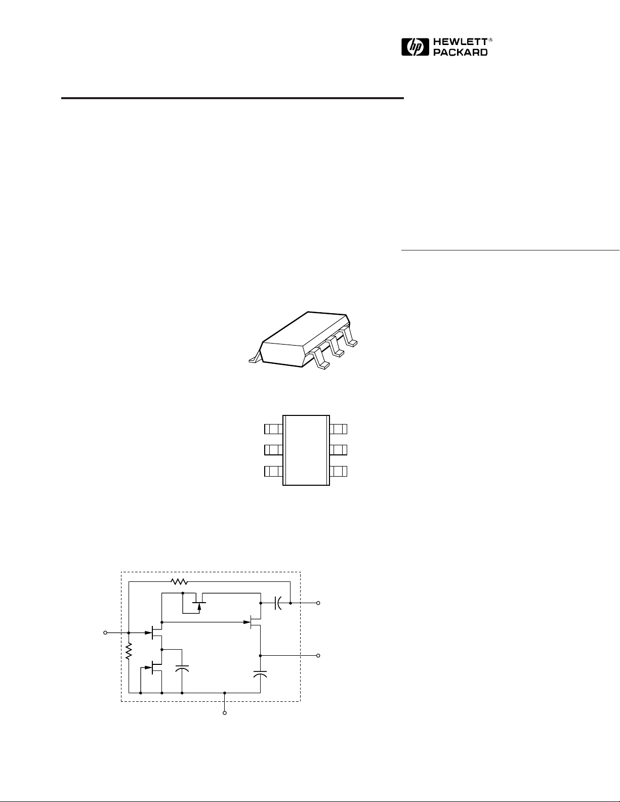
Equivalent Circuit
RF
INPUT
3
Surface Mount SOT-363 (SC-70) Package
Pin Connections and Package Marking
GND
1
87
GND
2
INPUT
Note:
Package marking provides orientation
and identification.
3
6
RF
OUTPUT
4
V
dd
6
5
4
OUTPUT
GND
V
dd
Description
Hewlett-Packard’s MGA-87563 is
an economical, easy-to-use GaAs
MMIC amplifier that offers low
noise and excellent gain for
applications from 0.5 to 4 GHz.
Packaged in an ultra-miniature
SOT-363 package, it requires half
the board space of a SOT-143
package.
With the addition of a simple
shunt-series inductor at the input,
the device is easily matched to
achieve a noise of 1.6 dB at
2.4␣ GHz. For 2.4 GHz applications
and above, the output is well
matched to 50 Ohms. Below
2␣ GHz, gain can be increased by
using conjugate matching.
The circuit uses state-of-the-art
PHEMT technology with selfbiasing current sources, a sourcefollower interstage, resistive
feedback, and on-chip impedance
matching networks. A patented,
on-chip active bias circuit allows
operation from a single +3 V or
+5␣ V power supply. Current
consumption is only 4.5 mA,
making this part ideal for battery
powered designs.
5965-9688E
GROUND
1, 2, 5
6-234

Absolute Maximum Ratings
Absolute
Symbol Parameter Units Maximum
V
dd
V
in
V
out
P
in
T
ch
T
STG
Device Voltage, RF V 6
Output to Ground
RF input or RF Output V +0.5
Voltage to Ground –1.0
CW RF Input Power dBm +13
Channel Temperature °C 150
Storage Temperature °C -65 to 150
[1]
Thermal Resistance
θ
= 160°C/W
ch-c
Notes:
1. Operation of this device above any one
of these limits may cause permanent
damage.
2. T
= 25°C (T
C
temperature at the package pins where
contact is made to the circuit board).
is defined to be the
C
[2]
:
MGA-87563 Electrical Specifications
[3]
, T
= 25°C, ZO = 50 Ω, V
C
= 3 V
dd
Symbol Parameters and Test Conditions Units Min. Typ. Max.
[3]
G
NF
test
test
NF
[3]
o
Optimum Noise Figure f = 0.9 GHz dB 1.9
f = 2.0 GHz 11 14
f = 2.0 GHz 1.8 2.3
(Tuned for lowest noise figure) f = 1.5 GHz 1.6
f = 2.0 GHz 1.6
f = 2.4 GHz 1.6
f = 4.0 GHz 2.0
G
a
Associated Gain at NF
O
f = 0.9 GHz dB 14.6
(Tuned for lowest noise figure) f = 1.5 GHz 14.5
f = 2.0 GHz 14.0
f = 2.4 GHz 12.5
f = 4.0 GHz 10.3
P
1dB
Output Power at 1 dB Gain Compression f = 0.9 GHz dBm -2.0
f = 1.5 GHz -1.8
f = 2.0 GHz -2.0
f = 2.4 GHz -2.0
f = 4.0 GHz -2.6
IP
3
Third Order Intercept Point f = 2.4 GHz dBm +8
VSWR Output VSWR f = 2.4 GHz 1.8
I
dd
Device Current mA 4.5
Note:
3. Guaranteed specifications are 100% tested in the circuit in Figure 10 in the Applications Information section.
6-235

MGA-87563 Typical Performance, T
5
20
= 25° C, V
C
= 3 V
dd
0
4
3
+85
2
NOISE FIGURE (dB)
1
0
0.5
1.5 2.5 3.5
FREQUENCY (GHz)
2.0
+25
-40
3.01.0
4.0
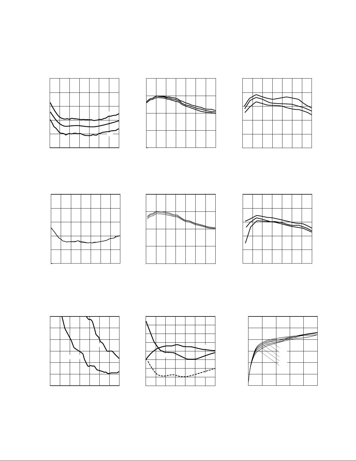
Figure 1. Minimum Noise Figure
(Optimum Tuning) vs. Frequency and
Temperature.
5
4
3
2
NOISE FIGURE (dB)
1
15
10
5
ASSOCIATED GAIN (dB)
0
0.5
1.0 2.5 3.5
2.0
1.5
FREQUENCY (GHz)
Figure 2. Associated Gain (Optimum
Tuning) vs. Frequency and
Temperature.
20
15
3.3 V
3.0 V
2.7 V
10
5
ASSOCIATED GAIN (dB)
3.0
-1
-2
-3
P 1 dB (dBm)
-4
-5
0.5
1.0 1.5 2.5 3.5
FREQUENCY (GHz)
2.0
4.0
-40
+25
+85
Figure 3. Output Power for 1 dB Gain
Compression (into 50 Ω) vs.
Frequency and Temperature.
0
-1
3.3 V
3.0 V
2.7 V
-2
-3
P 1dB (dBm)
-4
3.0
4.0
-40
+25
+85
3.3 V
3.0 V
2.7 V
0
0.5
1.0 1.5 2.5 3.5
2.0
FREQUENCY (GHz)
3.0
4.0
Figure 4. Minimum Noise Figure
(Optimum Tuning) vs. Frequency and
Voltage.
4.0
3.5
3.0
2.5
VSWR (n:1)
2.0
1.5
1.0
0.5
OUTPUT
1.5 3.52.5
FREQUENCY (GHz)
2.0
INPUT
3.0
4.01.0
Figure 7. Input and Output VSWR
(into 50 Ω) vs. Frequency.
0
0.5
1.0 2.5 3.5
2.0
FREQUENCY (GHz)
3.01.5
Figure 5. Associated Gain (Optimum
Tuning) vs. Frequency and Voltage.
5.0
4.5
4.0
3.5
3.0
2.5
2.0
NOISE FIGURE (dB)
1.5
1.0
0.5
NF 50
1.5
1.0 2.5 3.5
FREQUENCY (GHz)
2.0
3.0
Ga 50
NF OPT
4.0
Figure 8. 50 Ω Noise Figure and
Associated Gain vs. Frequency.
4.0
0.5
1.0 2.5 3.5
2.0
FREQUENCY (GHz)
-5
Figure 6. Output Power for 1 dB Gain
Compression (into 50 Ω) vs.
Frequency and Voltage.
20
15
10
5
ASSOCIATED GAIN (dB)
0
6
5
4
3
2
CURRENT (mA)
1
0
0
1
2
VOLTAGE (V)
Figure 9. Device Current vs. Voltage.
+85
+50
+25
-40
3.01.5
0
3
4.0
4
5
6-236
 Loading...