HP MGA-86576-TR1, MGA-86576-STR Datasheet

1.5 – 8 GHz Low Noise GaAs
MMIC Amplifier
Technical Data
MGA-86576
Features
• 1.6 dB Noise Figure at 4 GHz
• 23 dB Gain at 4 GHz
• +6 dBm P
at 4 GHz
1dB
• Single +5 V Bias Supply
Applications
• LNA or Gain Stage for 2.4
GHz and 5.7 GHz ISM Bands
• Front End Amplifier for GPS
Receivers
• LNA or Gain Stage for PCN
and MMDS Applications
• C-Band Satellite Receivers
• Broadband Amplifier for
Instrumentation
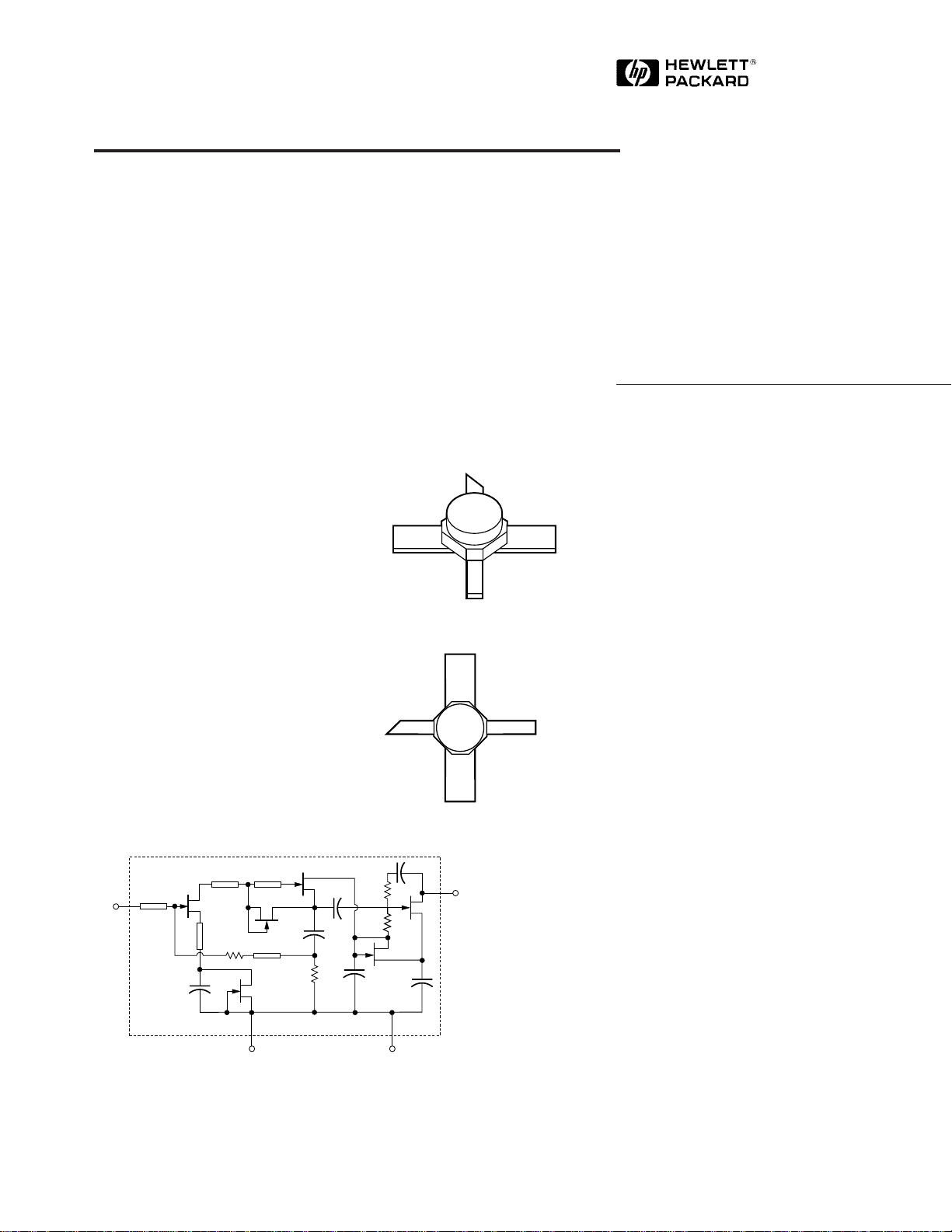
Schematic Diagram
RF
INPUT
1
Surface Mount Ceramic Package
Pin Connections
4 GROUND
GROUND
RF OUTPUT
AND V
d
RF INPUT
13
865
2
RF OUTPUT
AND V
d
3
Description
Hewlett-Packard’s MGA-86576 is
an economical, easy-to-use GaAs
MMIC amplifier that offers low
noise and excellent gain for
applications from 1.5 to 8 GHz.
The MGA-86576 may be used
without impedance matching as a
high performance 2 dB NF gain
block. Alternatively, with the
addition of a simple series
inductor at the input, the device
noise figure can be reduced to
1.6␣ dB at 4 GHz.
The circuit uses state-of-the-art
PHEMT technology with selfbiasing current sources, a sourcefollower interstage, resistive
feedback, and on chip impedance
matching networks.
A patented, on-chip active bias
circuit allows operation from a
single +5 V power supply. Current
consumption is only 16 mA.
5965-9687E
These devices are 100% RF tested
to assure consistent performance.
24GROUNDGROUND
6-228

Absolute Maximum Ratings
Absolute
Symbol Parameter Units Maximum
V
d
V
g
P
in
T
ch
T
STG
Device Voltage, RF output V 9
to ground
Device Voltage, RF input V +0.5
to ground -1.0
CW RF Input Power dBm +13
Channel Temperature °C 150
Storage Temperature °C -65 to 150
[1]
Thermal Resistance
θ
= 110°C/W
ch-c
Notes:
1. Operation of this device above any one
of these limits may cause permanent
damage.
2. T
= 25°C (T
c
temperature at the package pins where
contact is made to the circuit board).
is defined to be the
c
[2]
:
MGA-86576 Electrical Specifications, T
= 25° C, Zo = 50 Ω, V
C
= 5 V
d
Symbol Parameters and Test Conditions Units Min. Typ. Max.
Gp Power Gain (|S21|2) f = 1.5 GHz dB 21.2
f = 2.5 GHz 23.7
f = 4.0 GHz 20 23.1
f = 6.0 GHz 19.3
f = 8.0 GHz 15.4
NF
50
50 Ω Noise Figure f = 1.5 GHz dB 2.2
f = 2.5 GHz 1.9
f = 4.0 GHz 2.0 2.3
f = 6.0 GHz 2.3
f = 8.0 GHz 2.5
NF
o
Optimum Noise Figure f = 1.5 GHz dB 1.6
(Input tuned for lowest noise f = 2.5 GHz 1.5
figure) f = 4.0 GHz 1.6
f = 6.0 GHz 1.8
f = 8.0 GHz 2.1
P
1dB
Output Power at 1 dB Gain f = 1.5 GHz dBm 6.4
Compression f = 2.5 GHz 7.0
f = 4.0 GHz 6.3
f = 6.0 GHz 4.3
f = 8.0 GHz 3.8
IP
3
Third Order Intercept Point f = 4.0 GHz dBm 16.0
VSWR Input VSWR f = 1.5 GHz 3.6:1
f = 2.5 GHz 3.3:1
f = 4.0 GHz 2.2:1 3.6:1
f = 6.0 GHz 1.4:1
f = 8.0 GHz 1.2:1
Output VSWR f = 1.5 GHz 2.5:1
f = 2.5 GHz 2.1:1
f = 4.0 GHz 1.7:1
f = 6.0 GHz 1.4:1
f = 8.0 GHz 1.3:1
I
d
Device Current mA 9 16 22
6-229
 Loading...