

Page 1
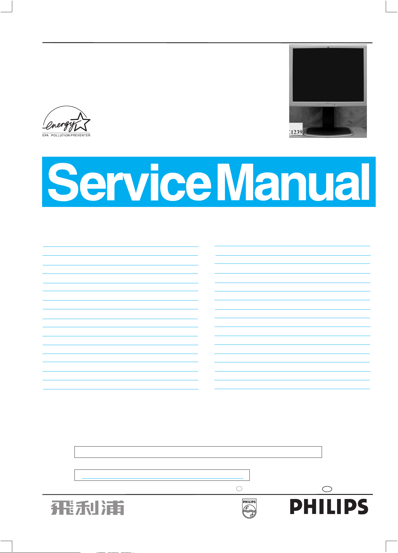
20" TFT LCD Colour Monitor
Service
Service
Service
TABLE OF CONTENTS
Description Page
Important Safety Notice ---------------------------------- 2
Technical Data ------------------------------------------ 3~4
Connection to PC, Front Control--------------------- 5~6
OSD User Mode-------------------------------------------- 7
OSD Lock/Unlock--- --- -----------------------------------8
Troubleshooting------------ --------- -- -------------------9
Safety Test Requirements-------------------------------10
Mechanical Instructions----------------------------- 11~12
Wiring Diagram-------------------------------------------- 13
Display Adjustment,Aging Mode -----------------------14
Electrical Instructions----------------------------------- 15
DDC Instructions-------------- ---------------------- 16~20
DDC Hex Data---------------------------------------- 21~22
Firmware upgraded for CPU -----------------------23~24
Block diagram-----------------------------------------25~26
DVI/DSUB Diagram---------------------------------------27
ADC Diagram---------------------------------------------- 28
HP L2035
FJ6B2S/76
Horizontal frequencies
30-94kHz
Description Page
TMSD RX Diagram-------------------------------------- 29
LVDS Diagram------------------------------------------- 30
SCALER Diagram--------------------------------------- 31
VIDEO Diagram------------------------------------------32
MEMORY/CLKGEN Diagram--------------------------33
I/O CONTROL Diagram---------------------------------34
POWER SUPPLY Diagram-----------------------------35
POWER + INVERTER Diagram------------------ 36~37
Scaler Panel (C.B.A.)------------------------------ 38~39
Control Diagram & Panel (C.B.A.) --------------------40
Power +Inverter Panel(C.B.A.)------------------- 41~42
RIepair Flow Chart-----------------------------------43~45
Exploded View ------------------------------------------- 46
Recommended
Spare parts list--------------------------------------- 48~51
General Product Specification-------------------- 52~76
parts list-- ----- ------------------------47
SAFETY NOTICE
ANY PERSON ATTEMPTING TO SERVICE THIS CHASSIS MUST FAMILIARIZE HIMSELF WITH THE CHASSIS
AND BE AWARE OF THE NECESSARY SAFETY PRECAUTIONS TO BE USED WHEN SERVICING ELECTRONIC
EQUIPMENT CONTAINING HIGH VOLTAGES.
CAUTION: USE A SEPARATE ISOLATION TRANSFORMER FOR THIS UNIT WHEN SERVICING.
REFER TO BACK COVER FOR IMPORTANT SAFETY GUIDELINES
Published by BU Monitor Printed in Taiwan Copyright reserved Subject to modification M Oct. 24 2003
GB
3138 106 10318
Page 2

2
HP L2035
Go to cover page
Important Safety Notice
Proper service and repair is important to the safe, reliable
operation of all HP Consumer Electronics Company**
Equipment. The service procedures recommended by
HP and described in this service manual are effective
methods of performing service operations. Some of these
service operations require the use of tools specially designed
for the purpose. The special tools should be used when and
as recommended.
It is important to note that this manual contains various
CAUTIONS and NOTICES which should be carefully read in
order to minimize the risk of personal injury to service
personnel. The possibility exists that improper service
methods may damage the equipment. It is also important to
understand that these CAUTIONS and NOTICES ARE NOT
EXHAUSTIVE. HP could not possibly know, evaluate and
advise the service trade of all conceivable ways in which
service might be done or of the possible hazardous
consequences of each way. Consequently, HP has not
undertaken any such broad evaluation. Accordingly, a
servicer who uses a service procedure or tool which is not
recommended by HP must first satisfy himself thoroughly that
neither his safety nor the safe operation of the equipment will
be jeopardized by the service method selected.
* * Hereafter throughout this manual, HP Consumer
Electronics Company will be referred to as HP.
WARNING
Critical components having special safety characteristics are
identified with a by the Ref. No. in the parts list and
enclosed within a broken line*
(where several critical components are grouped in one area)
along with the safety symbol on the schematics or
exploded views.
Use of substitute replacement parts which do not have the
same specified safety characteristics may create shock, fire,
or other hazards.
FOR PRODUCTS CONTAINING LASER :
DANGER-
CAUTION-
CAUTION-
TO ENSURE THE CONTINUED RELIABILITY OF THIS
PRODUCT, USE ONLY ORIGINAL MANUFACTURER'S
REPLACEMENT PARTS, WHICH ARE LISTED WITH THEIR
PART NUMBERS IN THE PARTS LIST SECTION OF THIS
SERVICE MANUAL.
Invisible laser radiation when open.
AVOID DIRECT EXPOSURE TO BEAM.
Use of controls or adjustments or
performance of procedures other than
those specified herein may result in
hazardous radiation exposure.
The use of optical instruments with this
product will increase eye hazard.
Take care during handling the LCD module with backlight
unit
- Must mount the module using mounting holes arranged in four
corners.
- Do not press on the panel, edge of the frame strongly or electric
shock as this will result in damage to the screen.
- Do not scratch or press on the panel with any sharp objects, such
as pencil or pen as this may result in damage to the panel.
- Protect the module from the ESD as it may damage the electronic
circuit (C-MOS).
- Make certain that treatment person s body are grounded through
wrist band.
- Do not leave the module in high temperature and in areas of high
humidity for a long time.
- Avoid contact with water as it may a short circuit within the module.
- If the surface of panel become dirty, please wipe it off with a soft
material. (Cleaning with a dirty or rough cloth may damage the
panel.)
Under no circumstances should the original design be
modified or altered without written permission from HP. HP
assumes no liability, express or implied, arising out of any
unauthorized modification of design.
Servicer assumes all liability.
* Broken Line
Page 3
Technical Data
HP L2035
Go to cover page
3
Technical Specifications
1. LCD monitor
Screen size : 359 mm x 287 mm
Maximal resolution :1600x1200 pixels
2.1 LCD Panel
Type NR. : LM201U04 (LG.PHILIPS)
Outline dimensions : 432.0(H)331.5(V)25.0(D) (Typ) mm
Pitch ( mm ) : 0.255 (per one triad) x 0.0.255mm
Color pixel arrangement: RGB vertical stripes
Display surface : low reflection, antiglare with hard coating
Color depth : 16777216 colors (8 bits)
Backlight : Six CCFL's
Active area(WxH) : 408x306mm (20.1 diagonal)
View angle : Horizontal & Vertical 170 degree (CR>5)
Contrast ratio : 300:1
White luminance : 250 nits (Typ)
2.2 Scanning frequencies
2.3 Video dot rate : < 205 MHz
2.4 Power input : 90-264 V AC, 50/60 +/- 2 Hz
2.5 Power consumption : < 75 W maximum
2.6 Dimensions : 466 * 460 * 220 mm
2.7 Weight : 9.5 KGS
2.8 Functions :
2.9 Ambient temperature : 5 C - 35 C
Hor. : 30 - 94 KHz
Ver. :48-85Hz
(1) D-shell analog R/G/B separate inputs, H/V sync separated,
Composite (H+V) TTL level, SOG sync
(2) DVI digital Panel Link TMDS input
(3) CVBS Video :1Vp-p,75 Ohm
(4) S-Video :Y-1Vp-p,75 Ohm
C-0.3Vp-p,75 Ohm
OO
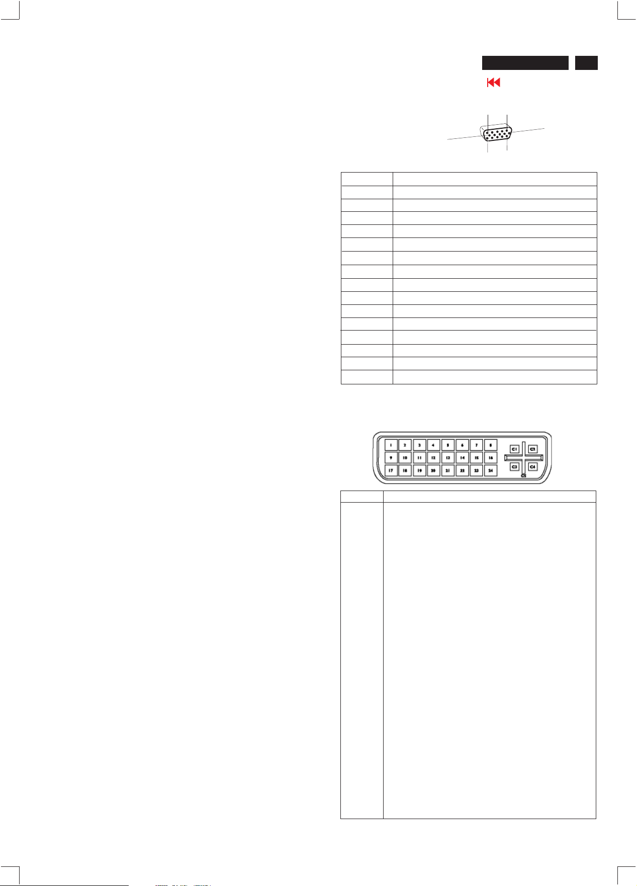
Pin Assignment
D-Sub connector
10
Pin No. Assignment
1 Red video input
2 Green video input / Sync On Green
3 Blue video input
4 Sense (Ground)
5 Not connected
6 Red video ground
7 Green video ground
8 Blue video ground
9NC
10 Sync. ground
11 Sense Ground
12 Bi-directional data
13 H/H+V Sync
14 V. Sync
15 Data Clock
15
1
5
6
11
The digital/analog DVI-I connector contains 29 signal contacts
organized in three rows of eight contacts. Signal pin
assignments are listed in the following table:
3.1 Interface signals
The input signals can be applied in three different modes :
1). D-shell Analog
Input signal : Video, Hsync., Vsync
Video : 0.7 Vp-p, input impedance, 75 ohm @DC
Sync. : Separate sync TTL level , input impedance 2k2 ohm terminate
Hor. sync Positive/Negative
Ver. sync Positive/Negative
Composite sync TTL level, input impedance 2k2 ohm
terminate (Positive/Negative)
Sync on green video 0.3 Vp-p Negative
(Video 0.7 Vp-p Positive)
2). Intel DVI Digital
Input signal : Single channel TMDS signal
3.1 Interface
3.2.1 D-Sub Cable
Length : 1870 mm (fixed) /with H-sync
impedence 50 Ohm +/- 10%
Connector type : D-sub male with DDC2B pin
assignments.
Blue connector thumb-operated jack screws
Pin No.
Description
1 TMDS data22 TMDS data2+
3 TMDS data2 shield
4NC
5NC
6 DDC clock
7 DDC data
8 Analog V-sync
9 TMDS data110 TMDS data1+
11 TMDS data1 shield
12 NC
13 NC
14 +5V
15 Ground(return for +5V and H/Vsync)
16 Hot plug detect
17 TMDS data018 TMDS data0+
19 TMDS data0 shield
20 NC
21 NC
22 TMDS clock shield
23 TMDS clock+
24 TMDS clock-
C1 Analog R
C2 Analog G
C3 Analog B
C4 Analog H-sync
C5 Analog GND (Analog R, G, Breturn)
Page 4

4
HP L2035
Go to cover page
Technical Data(Continued)
Recognizin g Pr es et Dis play Resolu tions
The display resolutions listed below are the most commonly used
modes and are set as factory defaults. This monitor automatically
recognizes these preset modes and they will appear properly sized
and centered on the screen.
Fact or y Pr es et Dis play Mod es
Pr es et P ix el For ma t
1640x480 31.5 60.0
2 6 40 x 480 37.5 75.0
3 6 40 x 480 43.3 85.0
4 720 x 4 00 31.5 70.1
5800x600 37.9 60.3
6 800 x 600 53.7 85.1
78 32x624 49.7 75.0
8 1024x768 48.4 60.0
9 1024x768 60.0 75.0
10 1024 x 768 68.7 85.0
11 115 2 x 870 69.0 75.1
12 1152 x 90 0 61.8 66.0
13 1280 x 960 60.0 60.0
14 1280 x 10 24 64.0 60.0
15 1280 x 10 24 80.0 75.0
16 1280 x 10 24 91.2 85.0
17 1600 x 1200 75.0 60.0
18 1600 x 1200 93.8 75.0
Ho rz F r eq
(kHz) Ver t Fr eq (Hz)
(Sun Mode II)
Usin g t h e Ener gy S aver Featur e
When the monitor is in its normal operating mode, the monitor
uses less than 75 watts of power and the Power light is green.
The monitor also supports a reduced power state. The reduced
power state will be entered into if the monitor detects the absence
of either the horizontal sync signal and/or the vertical sync signal.
Upon detecting the absence of these signals, the monitor screen is
blanked, the backlight is turned off, and the Power light is turned
amber. When the monitor is in the reduced power state, the
monitor will utilize less than 3 watts of power. There is a brief
warm up period before the monitor will return to its normal
operating mode.
Refer to your computer manual for instructions on setting energy
saver features (sometimes called power management features).
By selecting settings in the monitor s Energy Saver utility, you
can also program the monitor to enter into the reduced power
state at a predetermined time. When the monitor s Energy Saver
utility causes the monitor to enter the reduced power state, the
Power light blinks amber.
En terinGUs er Mod es
The video controller signal may occasionally call for a mode that
is not preset if:
You are not using a Hewlett Packard standard graphics
adapter.
You are not using a preset mode.
If this occurs, you may need to readjust the parameters of the
monitor screen by using the on-screen display. Your changes can
be made to any or all of these modes and saved in memory. The
monitor automatically stores the new setting, then recognizes the
new mode just as it does a preset mode. In addition to the 18
factory preset modes, there are four user modes that can be
entered and stored.
Page 5
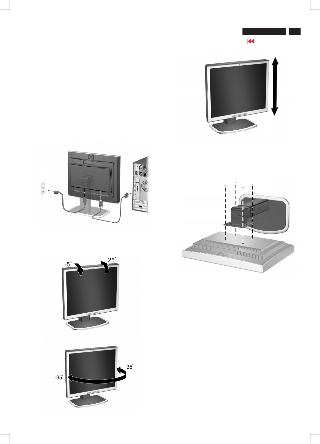
Connection to PC
S ettin g U p th e Monitor
To set up the monitor, ensure that the power is turned off to the
monitor, computer system, and other attached devices, then
follow these steps:
1. Place the monitor in a convenient, well-ventilated location
near your computer.
2. Connect one end of the monitor signal cable to the video
connector on the rear panel of the computer, and the other end
to the back of the monitor.
3. Connect the power cable to the back of the monitor, and the
other end of the power cable to an electrical wall outlet.
HP L2035
5
Go to cover page
Re movi n g th e M on i t or B as e
You can remove the monitor base to mount the monitor on a wall,
swing arm, or other mounting fixture. Read the caution and
warning statements below before beginning the procedure.
2. Remove the four screws as shown in the following
illustration.
4. Adjust the monitor as needed for your comfort using the
monitor s tilt, swivel, and height adjustment capabilities.
Moun tin g t h e Monitor
1. Remove the monitor base. Refer to R e moving the Monitor
Base steps in the previous section.
When the base is removed, four threaded mounting holes are
exposed on the monitor panel to be used for mounting
purposes. These mounting holes are spaced 100 mm apart
and are compliant with the Video Electronics Standards
Association (VESA) standard for mounting flat panel
displays.
2. Mount the monitor to a swing arm or other mounting fixture
by following the instructions included with the mounting
fixture to be used.
Page 6
6
HP L2035
Go to cover page
Front Panel Components
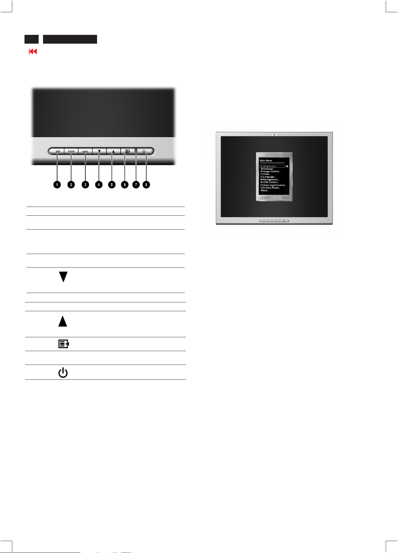
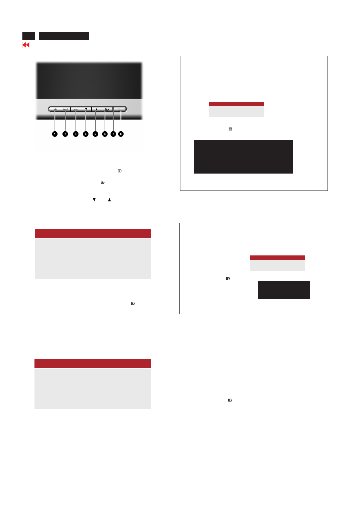
Fr on t P an el Compon en ts
N o. I con Con tr ol Function
1 P i P P i P b ut ton A ct i vat es Pi ctu r e i n P i ct ure ( Pi P )
2 input Si gnal Input
button
3 auto A uto button A uto ad justm entofdisplayed
4 OSD A djust Sel ect and adjust the OSD Menu
wi ndow
Si gnal input selection - scr olls
through VGA, DVI-A nalog,
DVI-Digital, Super video, and
composite video input
image
settings
Selects VGA in put when OSD is
not active
Adj u s tin g Monitor Set tin gs
Press the Menu button on the front panel of the monitor to view
the On Screen Display (OSD) Menu. The Main Menu window
pops up and you can make adjustments to your monitor s various
features. Use the left, right, up, and down arrow keys to make
your adjustments within the menu.
N o. Icon Con tr ol Fu n ction
5 OS D Adjust Select and adjust theOSD Menu
6 Menu button Launches the On-Screen Display
7 Pow er LE D Ful l pow er = G ree n
8 Power Sw itch Turns the monitor on and off
settings
Selects DVI-I input when OSD is
not active
(OSD) menu and selects func tions.
Sleep = Amber
Page 7
OSD User Mode
HP L2035
Go to cover page
7
Usin g the On-Sc r een Dis play
The adjustments for screen settings are located in the on-screen
display (OSD). Press the Menu button on the monitor's front
panel to view the OSD menu in one of six available languages.
The following table shows the menus and their functions at each
level:
OSD M en u Levels
Me nu Lev el1Me nu Lev el2Me nu Lev el3Me nu Lev el
4
Brightness Adjustment
Contrast A djustment
Image Control Auto
Co lor 930 0K
Language De utsch
Scale
Scale
Adjustme nt
Horizontal
Positi on
Ver ti cal
Positi on
Custom
Scaling
Sharpness Adjustment
Clock A djustment
Clock Phase A djustment
6500 K - sRGB
CustomColor Red, Green,
VideoColor Hue,
Espa ol
Adjusting
Message
Adjustment
Scale
Adjustment
Scale
Fi ll to S creen
Fill to Aspect
Ratio
One to One
Scale
Scale
Scale
Blue
Saturation
OSD M en u Levels
Me nu L ev el1Me nu L ev el2Me nu L ev el3Me nu Lev el
4
Francais
Italiano
Nederlands
Management Power Saver On/Off
Power O n
Recall
Mode Dis play On/Off
Serial Number (display seri al
Sleep T imer Set current&
Basic Menu
OSD Control H oriz onta l
VideoInput
Controls
Positi on
Ver ti cal
Positi on
OS D TimeoutAdjustment
OS D
Tr ansparenc y
VideoInput
Select
Selection
On/Off
Selection
Selection
number)
sleep time
Adjustment
Scale
Adjustment
Scale
Scale
Adjustment
Scale
Analog (VGA)
Analog (DVI)
Digital (DVI)
S -Vi deo
OSD M en u Lev els
Me nu Lev el1Me nu Lev el2Me nu Lev el3Me nu Lev el
4
Co mposite
Video
Auto Detect
Pi P Control PiP S ourc e Super Video
Co mposite
Video
PiP S ize Pi P O ff
Small
Medium
Large
Horizontal
Positi on
Ver ti cal
Positi on
Factory Reset Yes
No
Exit
Adj Scale
Adj Scale
Page 8
8
HP L2035
Go to cover page
OSD Lock/Unlock, Service Mode
Front control panel
To Lock/Unlock OSD function (User Mode)
The OSD function can be locked by pressing button for more than
10 seconds, the screen shows following windows for 3 seconds.
Everytime when you press or button, this message
appears
on the screen automatically. The & (brightness) ,
(input) hotkey are still functional for brightness and input signal
AUTO
INPUT
Access Service Mode (in USER MODE)
Method 1:
Step 1: Disconnect signal cable on Rear side of monitor.
Don't disconnect signal cable on PC side, because CPU will
detect pin-9 of D-SUB (15 pin connector).
(Monitor & PC are still ON.)
Bring up "CHECK CABLE CONNECTION" screen.
ATTENTION
CHECK CABLE CONNECTION
Step 2: Press MENU" " button for more than 15 seconds.
Bring up message as below.
SERVICE MODE
SERIAL NO. : 002DA03PA001
HOURS OF OPERATION: 000323
Leave service mode by either re-feed video signal or simply turn off
and on the power of monitor.
ATTENTION
OSD MAIN CONTROLS LOCKED
Locked OSD function can be released by pressing button for
more than 10 seconds again. While press "MENU" button for OSD
locked purpose, the screen will keep showing OSD MAIN
CONTROLS LOCKED u ntil OSD function locked and screen
automatically shows following window for 3 seconds.
ATTENTION
OSD MAIN CONTROLS UNLOCKED
Access Service Mode (in USER MODE)
Method 2:
Step 1:
- Turn off monitor.
- Disconnect signal cable on PC side.
- Turn on monitor.
Bring up "NO VIDEO INPUT"
(After 3 seconds)
Step 2: Press MENU" " button for more than 15 seconds.
Bring up "SERVICE MODE".
Leave service mode by either re-feed video signal or simply turn off
and on the power of monitor.
ATTENTION
NO VIDEO INPUT
SERVICE MODE
SERIAL NO. : 002DA03PA001
HOURS OF OPERATION: 000323
Access Service Mode (in USER MODE)
Method 3:
Step 1:
-PCoff.
- Signal cable connect to rear side of Monitor only.
- Turn on monitor.
Bring up "NO VIDEO INPUT"
Step 2: Press MENU" " button for more than 15 seconds.
Bring up "SERVICE MODE".
Leave service mode :simply turn off and on the power of monitor.
Page 9

Troubleshooting
Solving Common Problems:
Problem Possible Cause Solution
Screen is blank. Power cord is Connect the power cord.
Disconnected.
Power switch is turned Turn on the power.
Off.
Video cable is Connect the video cable
improperly connected. Properly.
Screen blanking utility is Depress any key on the
active. keyboard or move
themouse to inactivate the
screen blanking utility.
Image appears Brightness and contrast Press the Minus button on
blurred, indistinct, or are too low. the monitor front panel to
too dark. auto-adjust the screen. If that
does not work, press the
menu button to open the
basic OSD Menu, and
adjust the brightness and
contrast scales as needed.
HP L2035
Go to cover page
9
Image is not Position may need When OSD is inactive,
Centered. adjustment. press (minus button) to
Check Video Monitor video cable is Connect the 15-pin monitor
Cable is displayed disconnected. video cable to the VGA
on screen. connector on the computer.
Input Signal Out of Video resolution and/or Restart your computer and
Range is displayed refresh rate are set enter Windows Safe Mode
on screen. higher than what your by pressing the F6 Function
monitor supports. key when the computer starts
auto-adjust the screen
image.
Press the Menu button to
access the Advanced OSD
menu. Select Image
Control/Horizontal Position
or Vertical Position to adjust
the horizontal or vertical
position of the image.
Be sure that the computer
power is off while
connecting the video cable.
to boot up. Change your
settings to a supported
setting. Restart your
computer so that the new
settings take effect.
Page 10
10
HP L2035
Go to cover page
Safty Test Requirements
All units that are returned for service or repair must pass the
original manufactures safety tests. Safety testing requires both
and testing.Hipot Ground Continuity
HI-POT TEST INSTRUCTION
1. Application requirements
1.1 All mains operated products must pass the Hi-Pot test as
described in this instruction.
1.2 This test must be performed again after the covers have
been refitted following the repair, inspection or modification
of the product.
2. Test method
2.1 Connecting conditions
2.1.1 The test specified must be applied between the parallel-
blade plug of the mainscord and all accessible metal
parts of the product.
2.1.2 Before carrying out the test, reliable conductive
connections must be ensured and thereafter be
maintained throughout the test period.
2.1.3 The mains switch(es) must be in the "ON" position.
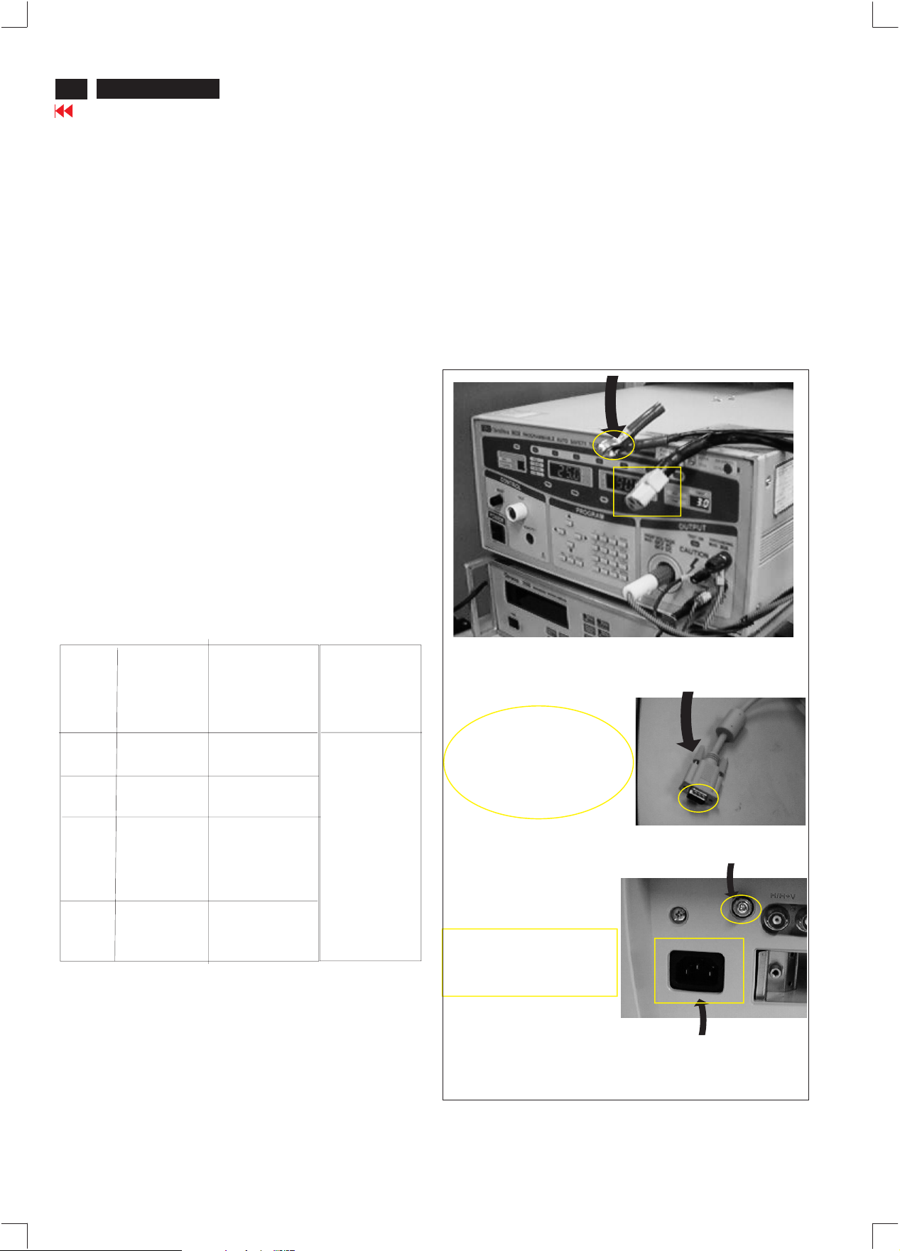
3. Equipments and Connection
3.1. Equipments
For example :
- ChenHwa 9032 PROGRAMMABLE AUTO SAFETY
TESTER
- ChenHwa 510B Digital Grounding Continuity Tester
- ChenHwa 901 (AC Hi-pot test), 902 (AC, DC Hi-pot test)
Withstanding Tester
3.2. Connection
* Turn on the power switch of monitor before Hipot and
Ground Continuity testing.
Clip
Clip
2.2 Test Requirements
All products should be HiPot and Ground Continuity tested as
follows:
Condition HiPot Test for HiPot Test for Ground Continuity
products where products where Test requirement
the mains input the mains input is
range is Full 110V AC(USA
range(or 220V type)
AC)
Test 2820VDC 1700VDC Test current:
voltage (2000VAC) (1200VAC) 25A,AC
Test time:
Test time 3 seconds 1 second 3 seconds(min.)
(min.) Resistance
required:
Trip set at 100 uA 5 mA <=0.09+R ohm,
current for Max. R is the
(Tester) limitation; set resistance of
at 0.1 uA for the mains cord.
Min. limitation
Ramp set at 2
time seconds
(Tester)
(ChenHwa 9032 tester)
Video cable
Connect the "video cable"
or "grounding screw"
to the CLIP on your tester.
Grounding screw
Connect the power cord
to the monitor.
2.2.1 The test with AC voltage is only for production purpose,
Service center shall use DC voltage.
2.2.2 The minimum test duration for Quality Control Inspector
must be 1 minute. No breakdown during the test.
2.2.3 The test voltage must be maintained within the specified
voltage + 5%.
2.2.4 The grounding blade or pin of mains plug must be
conducted with accessible metal parts.
4. Recording
Hipot and Ground Continuity testing records have to be kept for
a period of 10 years.
Power outlet
(Rear view of monitor)
Page 11
Mechanical Instructions
HP L2035
Go to cover page
11
Front view as shown
in Fig. 1.
Fig. 1
To use the height adjustment
base in Fig. 2.
Fig. 2
Step 1 :
Disconnect screw and push
up and down the the monitor
as shown in Fig. 3.
BASE
After removing the base, turn the set over,then disconnect the 2 screws
Step 3 :
Remove Front Bezel by "-" screw driver on click holes to dig the back
cover as shown in Fig. 7 .
Front Bezel==>
Plastic clip (left & right) can be released by "-" screw driver as shown in
Fig.8&9.
screw
Fig. 7
Fig. 6
dig out here
screw
Fig. 4
Step 2 :
Lay the front bezel
1.
down
on a soft area to
prevent it from getting
scratched, defaced, or
broken.
2.Remove the four screws
as shown in Fig. 5.
3.Remove the monitor
base from the monitor
as shown in Fig. 5.
Fig. 3
Fig. 4
4 SCREWs
Disconnect screw
Fig. 8
Fig. 9
Step 4 :
Remove front bezel as shown in Fig. 10.
Fig. 5
Control panel ==>
Fig. 10
Page 12
12
HP L2035
Mechanical Instructions (Continued)
Go to cover page
Step 6 :
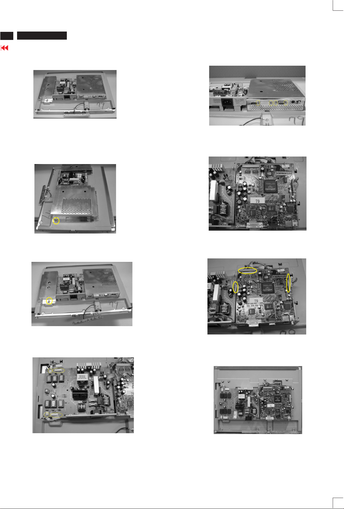
1.Take out LCD panel from back cover as shown in Fig. 11.
Step 10 :
1.Disconnect DVI and D-SUB hexagonal screw as shown Fig.15
.
Fig. 11
Step 7:
Remove scaler metal cover screws as shown in Fig. 12.
Metal Frame
Fig. 12
SCREW
Step 8 :
Remove power & inverter metal cover screws as shown in Fig. 13.
Fig. 15
2.Then remove metal shield as shown Fig. 16.
Step 11 :
Disconnect 1711,1701,1501 connector on scaler
as shown in Fig. 17.
1501
Metal Frame
Hexagonal screw
ard board
Metal Frame
Fig. 13
Step 9 :
Disconnect 1803 ,1807,1806,1804 connector on inverter board
as shown in Fig. 14.
Fig. 14
1806
1803
1804
1807
Fig. 17
Step 12 :
C
onnect 1803,1807,1806,1804 1711,1701,1501 connector on the
inverter+ power board and scaler
Fig. 18
1711
ard board as shown in Fig. 18.
1701
Page 13
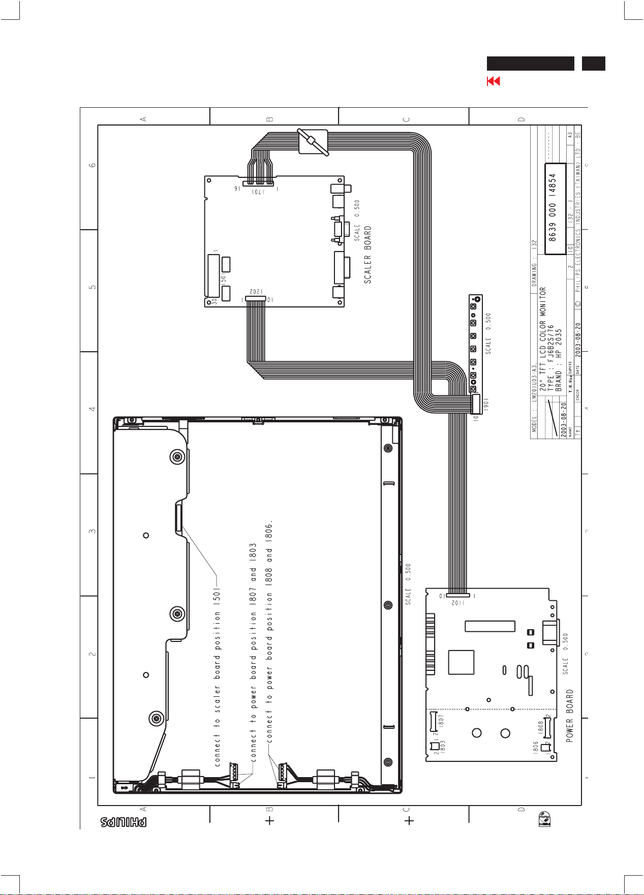
Wiring Diagram
HP L2035
Go to cover page
13
Page 14
14
HP L2035
Go to cover page
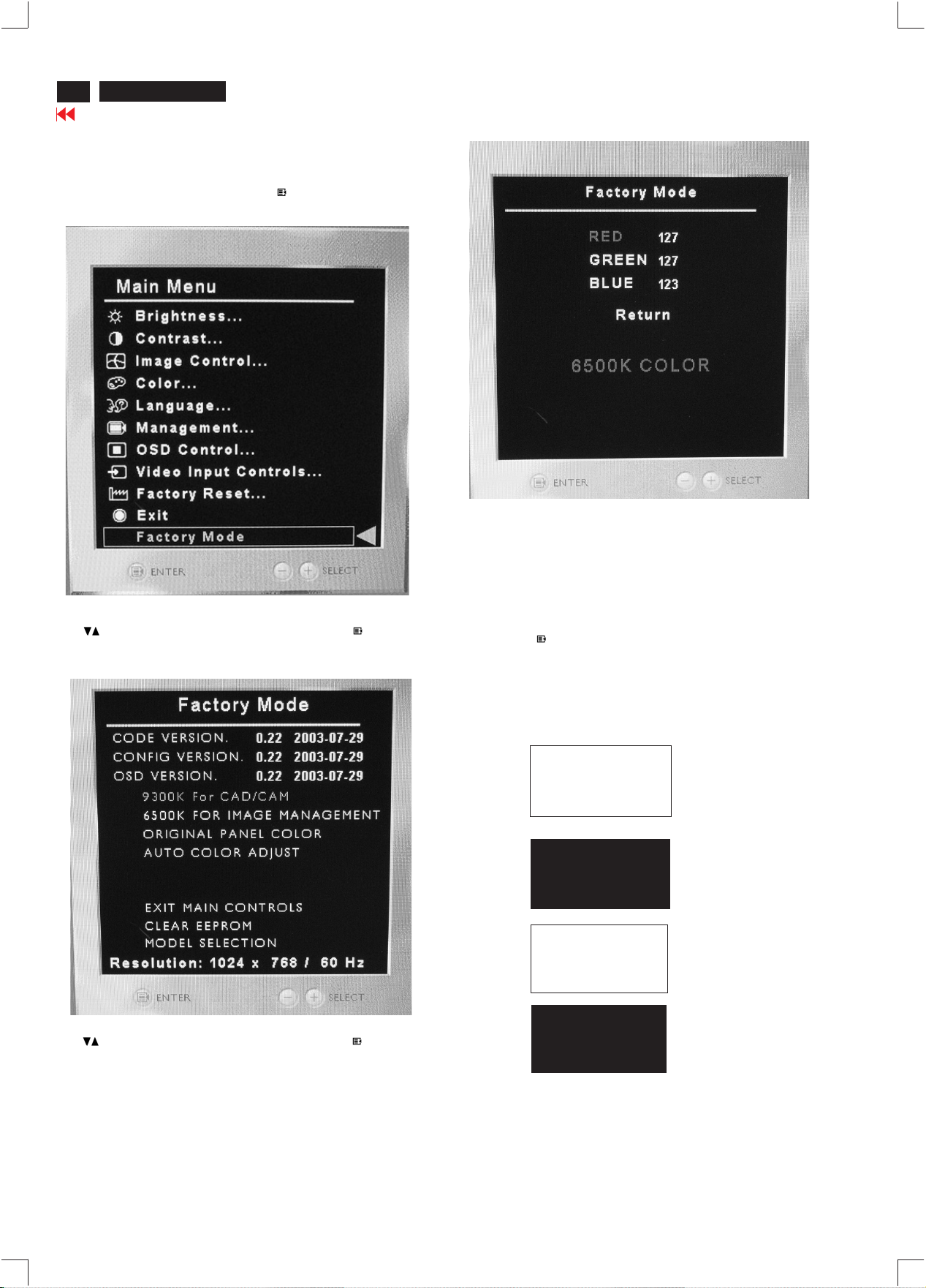
Factory mode Adjustment:
Display Adjustment , Aging Mode
Entering factory mode as Press and button
simultaneously and power ON as Fig. 1shown below.
Use buttons to Factory Mode to enter byMenu then
appearFig.2 as below
Menu auto
9300KRGB
6500KRGB
Color temperature gain adjustment. Use these menu items
to adjust the RGB gains of pre-amp for different color
temperatures, ranges from 0 to 255.
Access AGING Mode (Burn in mode) : IN Factory MODE
Step 1 :
Push Menu " " & " " buttons at the same time and power ONAuto
Step 2: Disconnect Interface (Signal) cable.
=> Bring up
"Full black pattern (if black, wait 5 seconds
around)"
or
"Full White pattern with character "Aging"
as below.
Use buttons to Factory Mode to enter byMenu then
9300K For CAD/CAM,6500K For IMAGE MANAGEMENT,
ORIGINAL PANEL COLOR,AITO COLOR ADJUST.
Bring up
After 5 seconds, bring up :
After 5 seconds, bring up :
:
Aging
Aging
After 5 seconds, bring up :
----------
----------Repeatly
How to return to Normal display (User Mode)
Method : reconnect the interface cable of LCD monitor.
Page 15
Electrical instructions
HP L2035
Go to cover page
15
1. General points
1.1 During the test and measuring, supply a distortion free AC
mains voltage to the apparatus via an isolated transformer with
low internal resistance.
1.2 All measurements mentioned hereafter are carried out at a
Normal mains voltage (90 - 132 VAC for USA version, 195 -264
VAC for EUROPEAN version, or 90 - 264 VAC for the model with
full range power supply, unless otherwise stated.)
1.3 All voltages are to be measured or applied with respect to
Ground, unless otherwise stated.
Note: don't use heat-sink as ground.
1.4 The test has to be done on a complete set including LCD panel
in a room with temperature of 25 +/- 5 degree C.
1.5 All values mentioned in these test instruction are only applicable
of a well aligned apparatus, with correct signal.
1.6 The letters symbols (B) and (S) placed behind the test
instruction denotes (B): carried out 100% inspection at
assembly line
(S): carried out test by sampling
1.7 The white balance (color temperature), has to be tested in
subdued lighted room.
1.8 Repetitive power on/off cycle are allowed.
1.9 All optical characteristics (including WHITE-D, Brightness, and
so on) are determined according to panel specification after
warming up approximate 30 minutes that brightness stability is
optimal, and follow strictly after panel specification.
2. Input signal
Signal Type
2.1.1 Analog Video: 0.7 Vp-p linear, positive polarity
Sync. : TTL level, separate, positive or negative polarity
Signal source : pattern generator format as attachment.
( Table 1 to 47 ) Reference generator : Quantumdada 802G
2.1.2 Digital Video : 600m Vp-p TMDS signal
2.1.3 CVBS Video : 1Vp-p, 75Ohm
2.1.4 S-Video : Y-1 Vp-p, 75 Ohm
2.2 Input signal Mode
Item H.Freq.
(KHz)
C-0.3V
p-p, 75 Ohm
Mode Resolution V.Freq.
(Hz)
1 31.469 IBM VGA 3H 720x400 70.087
2 31.469 IBM VGA 12H 640x480 59.940
10
3
4
5
6
7
8
9
11
12
13
37.500
43.27
37.879
VESA
VESA
VESA
53.67 VESA
49.700
48.363
60.023
68.68 VESA
68.700
61.80
60.00
MACINTOSH
VESA
VESA
MACINTOSH1152x870 75.000
SUN WS
VESA
640x480
640x480
800x600
800x600
832x624
1024x768
1024x768
1024x768
1152x900
1280x960 60.00
75.000
85.01
60.317
85.06
75.000
60.004
75.029
85.00
65.96
15
16
17
18
3.AC Power Board
3.0 Detach 1102 from the scalar board.
Check the O/P (output) voltage within 18 +/- 0.9 VDC, 3.3+/-0.15VDC
and the start up circuit
3.1.1
Set AC input at 264/90 V, add 3.1A loading to C2118 and DC O/P
voltage is 18 +/- 0.9V, Add1A load to C2003 and DC O/P voltage is
3.3V+/-0.15VDC (B)
3.1.2
Check switching frequency at 6112 Anode is 60KHz~175KHz at
normal load,17KHz +/- 3KHz at no load condition. (S)
3.2 Over Voltage protection test
If an over-voltage fault on the adapter output, the adapter should be
shut down before the output voltage exceeds 23V. (B)
3.2.1
Set the AC I/P : 264VAC.
3.2.2
Add a resistor 47Kohm in parallel with the 3131. (B)
3.2.3
Then the O.V.P. circuit should be activated before the output of the
adapter over 23V (B)
3.2.4
Take off the resistor 47Kohm and discharge C2118, the O/P should be
:18V +/-0.9V. (B)
3.3
Over load protection test
3.3.1
Set I/P AC power input at 264VAC
3.3.2
Rise the 18VDC output current higher than 5 Amp. The adapter
should be shut down before 7 Amp.(B)
3.4 Short Circuit protection test
3.4.1
Set AC input at 264V, O/P is 18V/3.33A.
3.4.2
Short 18VDC O/P, the I/P power consumption is less than 5 W. (B)
3.4.3
Open the short circuit, the 18VDC output should be resolved and
stable.
4.0DC/DC power supply
4.01
Detach 1102 to the scaler board before testing the function.
4.02
Apply 1.3Amp load to 3.3V at C2003 (B)
4.03
Check frequency at 6001 is 240KHz +/- 15KHz (S)
4.05
Check voltage at C2003 should be within the range 3.3V +/-
0.15V (B)
79.976 VESA
91.1
75.0
93.8
VESA 1280x1024
VESA 1600x1200
VESA
1280x1024
x1200 75
1600
75.025
85
60
14
63.981
VESA
1280x1024 60.020
Page 16
HP L2025
16
HP L2035
Go to cover page
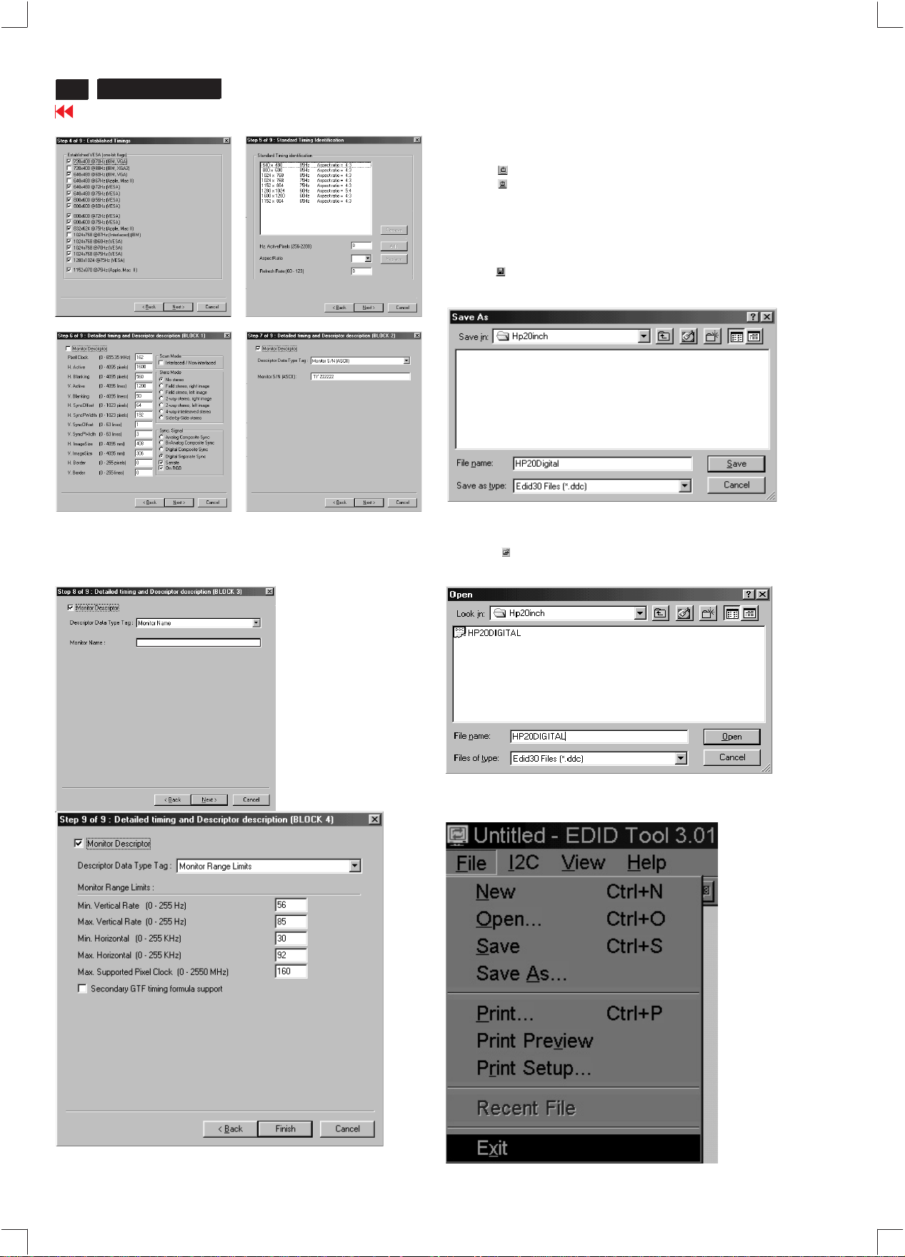
DDC Instructions
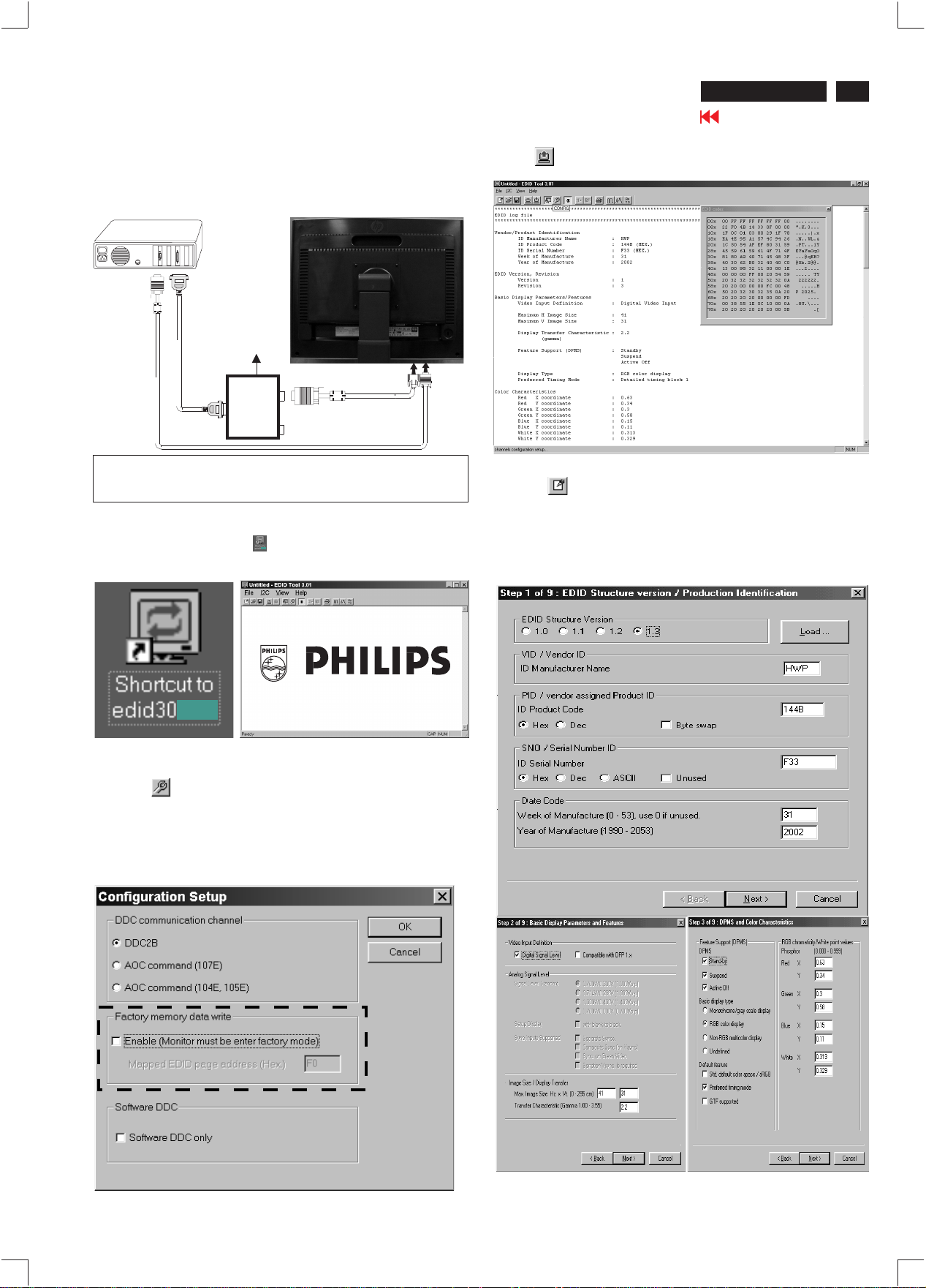
General
DDC Data Re-programming
In case the DDC data memory IC or main EEPROM which storage all
factory settings were replaced due to a defect, the serial numbers have
to be re-programmed.
It is advised to re-soldered DDC IC and main EEPROM from the old
board onto the new board if circuit board have been replaced, in this
case the DDC data does not need to be re-programmed.
Additional information
Additional information about DDC (Display Data Channel) may be
obtained from Video Electronics Standards Association (VESA).
Extended Display Identification Data(EDID) information may be also
obtained from VESA.
DDC EDID structure
For Analog interface: Standard Version 3.0
For Digital inferface: Standard Version 3.0
Structure Version 1.2
Structure Version 1.3
System and equipment requirements
1. An i486 (or above) personal computer or compatible.
2. Microsoft operation system Windows 95/98.
3. EDID301.EXE program (3138 106 10103) as shown in Fig. 1
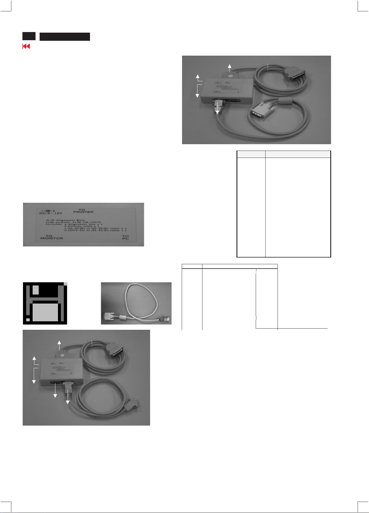
4. A/D Alignment kits (3138 106 10079):
inclusion : a. Alignment box x1 (as Fig. 2)
b. Printer cable x1
Note: The EDID301.EXE (Release Version 1.58 20000818)is a
windows-based program, which cannot be run in MS-DOS.
EDID301.EXE
Ver:1.58
Diskette with EDID301.EXE
c. (D-Sub) to (D-Sub) cable x1
d. (DVI-D) to (D-Sub) cable x1 (as Fig. 3)
Fig. 3Fig. 3
Fig. 1Fig. 1
(DVI-D) to (D-Sub) cable
To Printer
Fig. 2Fig. 2
To Printer
DC 8V~12V
Power
indicator
To Monitor
(Digital port)
A/D Alignment Kits - Digital connectionA/D Alignment Kits - Digital connection
Pin assignment
A. 15-pin D-Sub Connector
PIN No. SIGNAL
1 Red
2 Green/ SOG
3 Blue
4 Sense (GND)
5 Cable detect
6 Red GND
7 Green GND
8 Blue GND
9 +5V
10 Sync GND
11 Sense (GND)
12 Bi-directional data
13 H/H+V sync
14 V-sync
15 Data clock
B. DVI-D Connector
Pin No. Description
1 TMDS data22 TMDS data2+
3 TMDS data2 shield
4NC
5NC
6 DDC clock
7 DDC data
8 Analog V-sync
9 TMDS data110 TMDS data1+
11 TMDS data1 shield
12 NC
13 NC
14 +5V
15 Ground(return for +5V and H/V-sync)
16 Hot plug detect
17 TMDS data018 TMDS data0+
19 TMDS data0 shield
20 NC
21 NC
22 TMDS clock shield
23 TMDS clock+
24 TMDS clockC1 Analog R
C2 Analog G
C3 Analog B
C4 Analog H-sync
C5 Analog GND (Analog R, G, B return)
Configuration and procedure
DC 8V~12V
Power
indicator
To Monitor
Video Card
Video Card
A/D Alignment Kits - Analog connectionA/D Alignment Kits - Analog connection
Note: The alignment box has already build-in a batteries socket for
using batteries (9V) as power source. Pull out the socket by
remove four screws at the rear of box. Please do not forget that
remove batteries after programming. The energy of batteries can
only drive circuits for a short period of time.
There are threeips contained serial number on the circuit board,
Analog DDC IC (7202), Digital DDC IC (7201) and main
EEPROM (7362) which storage all factory settings. Following
descriptions are the connection and procedure for Analog DDC
IC and Digital DDC IC, the main EEPROM can be reprogrammed along with Analog IC by enable factory memory
data write function on the DDC program (EDID301.EXE).
Initialize alignment box
In order to avoid that monitor entering power saving mode due to
sync will cut off by alignment box, it is necessary to initialize
alignment box before running programming software (EDID301.EXE).
Following steps show you the procedures and connection.
Page 17
DDC Instructions
HP L2025
HP L2035
HP L2025
HP L2025
Go to cover page
25
7
17
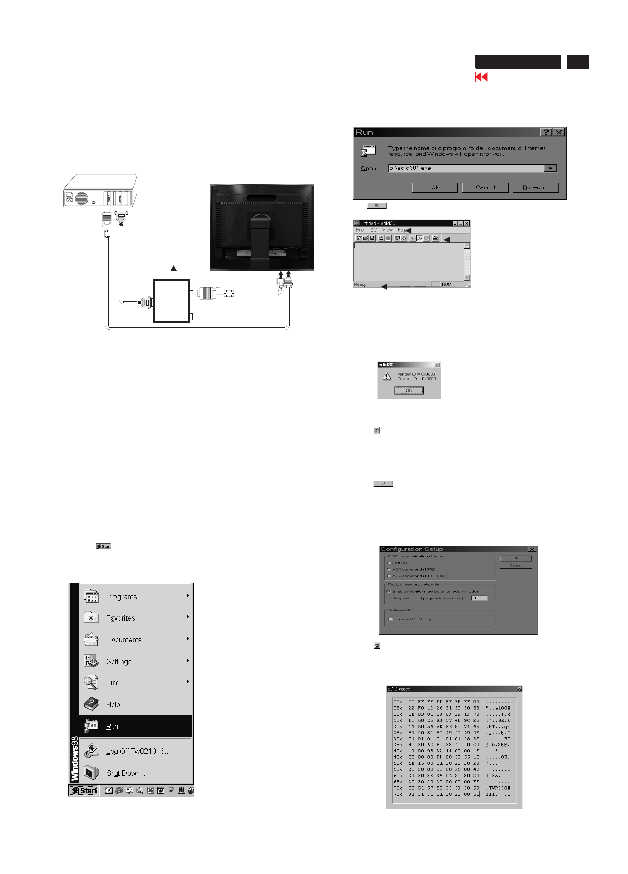
Step 1: Supply 8~12V DC power source to the Alignment box by
plugging a DC power cord or using batteries.
Step 2: Connecting printer cable and video cable of monitor as Fig. 4
Step 3: Run the EDID301.EXE program until the main menu appears.
This is for initialize alignment box.
1=DVI-I connector
PC
DC Power
8~12 V
~
~
To video card
Fig. 4
Note: DVI-Dto D-Sub adapter can be removed if graphic card of PC with
a DVI-D interface connector.
To printer port (LTP1)
Printer
Port
DVI-I to D-Sub cable
To
Monitor
To P C
D-Sub connector
2=D-SUB connector
2
1
3. At the submenu, type the letter of your computer's floppy disk drive
followed by :EDID301 (for example, A:\EDID301.exe,)
as shown in Fig. 6.
Fig. 6
4. Click button. The main menu appears (as shown on Fig. 7).
Command bar
Tools bar
Fig. 7
Status bar
Note:
If the connection is improper, you will see the following error
message before entering the main menu. Meanwhile, the
(read EDID) function will be disable. At this time, please make
sure all cables are connected correctly and fixedly, and the
procedure has been performed properly.
Re-programming DDC IC
Step 1: After initialize alignment box, connecting all cables and box as
Fig. 4
Step 2: Follow the steps on DDC re-programming instructions to staring
re-programming.
Re-programming Analog Device As Fig. 4
DDC re-programming instructions
Start on DDC program
Start Microsoft Windows.
1. Insert the disk containing EDID301.EXE program into floppy disk
drive.
2. Click , choose Run at start menu of Windows 95/98.
Loading DDC data from monitor
1. Click icon on the tools bar to bring up the Configuration Setup
windows as Fig.8
2. Select the DDC2B as the communication channel.
3. Enable Factory memory data write function and fill in page address
F0 to the block.
4. Disable Software DDC function.
5. Click button to confirm your selection.
Note: The Factory memory data write function will allow EDID301 to
rewrite serial numbers both Analog DDC IC and main EEPROM to
make sure both S/N are exactly the same. You may confirm the
function by checking the S/N at Product information of the OSD
menu after restarting the monitor.
Fig. 8
6. Click icon to read DDC EDID data from monitor. The EDID
codes will display on screen as following. (The EDID codes are
depend on the model.) Meanwhile, The status bar will indicate 00%
to 100% when reading.
Page 18
18
HP L2035
Go to cover page
DDC Instructions
Note:
During the loading, EDID301 will verify the EDID data which just
loaded from monitor before proceed any further function, once the
data structure of EDID can not be recognized, the following error
message will appear on the screen, as below. Please confirm
following steps to avoid this message.
1. The data structure of EDID was incorrect.
2. DDC IC that you are trying to load data is empty.
3. Wrong communication channel has set at configuration setup
Windows.
4. Cables loosed or poor contact of connection.
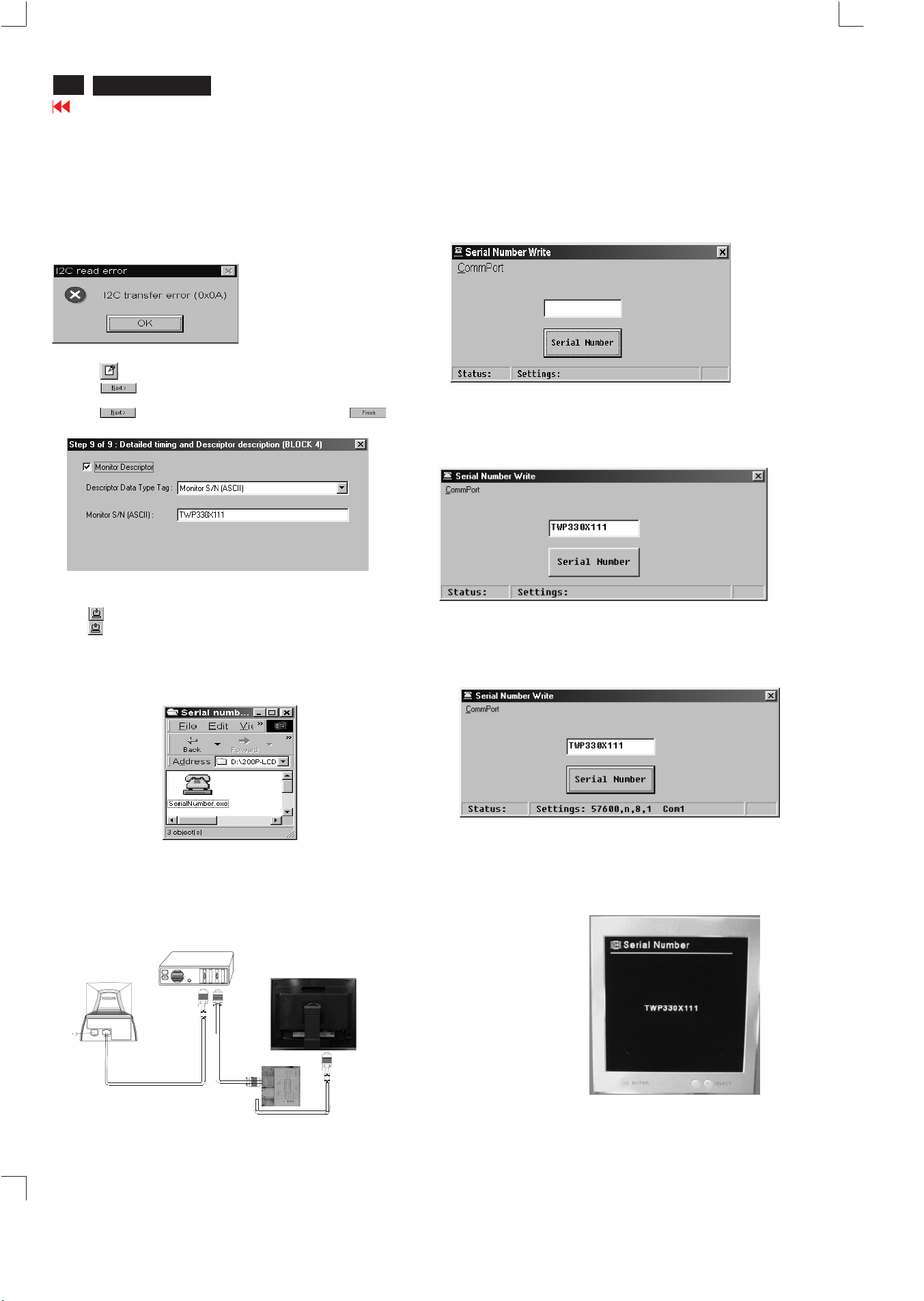
Modify DDC data (Serial No.)
1. Click icon on the toosl bar.
2. Click till the Step 9 of 9 window appears.
3. Type the new Serial No. (for example, TWP330X111).
4. Click till the last step window appears, then click to
exit the Step window.
Attention :
Before doing "SerialNumber.exe" in your windows 98 PC, The HPL2035 monitor
must be in the factory mode, then run following process as below.
Step 1: Double click "SerialNumber.exe"
Bring up: Fig. 3
Fig. 3
Fill out serial number of monitor.
For example "TWP330X111" as shown in Fig. 4.
Write DDC data to monitor
1. Click icon from the tools bar to starting rewrite DDC data.
2. Click for confirmation.
3. In order to match the same serial number in OSD with DDC data,
The following action should be executed.
*****************************************************************************
Change/update the serial number which should be proceeded
by application software "SerialNumber.exe" as shown in Fig. 1
*****************************************************************************
Fig. 1
*****************************************************************************
Connection :Using IIC & Rs232 Alignment Kits(3138 106 10198)
for Serial Number applicationFig.2.
*****************************************************************************
Monitor (A)
PC
25 pins
Com1 or
Com2
9 pins
Monitor (B)
Rear view of HP L2035
---------------->
Fig. 4
(click "Serial Number")
Step 2: Click "Serial Number" as shown in Fig. 5.
---->
Fig. 5
(Com port for application)
Bring up Fig. 5 with "57600,n,8,1 Com1"
Step 3: Verify "Serial Number" by OSD as shown in Fig. 6.
Press OK button
=>select "management"
=>press OK Button,then
=>select "Serial Number"
=>press OK Button
Bring up :
Fig. 6 for verification.
Connect to
Mains cord
Video cable
To video card
To Com1 or Com2 (PC)
9 pins
Fig. 6
Fig. 2
Fig. 9
Page 19
DDC Instructions (Continued)
HP L2035
Go to cover page
19
Re-programming Digital DDC IC
Connecting all cables and alignment box as shown in
Step 1:
Fig. 9.
1=DVI-I connector
PC
DC Power
8~12 V
~
~
To video card
Fig. 9
After connection for Digital DDC application, if it is still in Analog DDC
application of EDID301.
Exit EDID301 program before Digital DDC application.
Step 2: Initialize alignment box
(Shortcut of EDID301.EXE on
Double click EDID301 icon (as shown in Fig. 10) which is
on the screen of Windows Wallpaper.
Bring up main menu of EDID301 as shown in Fig. 11.
To printer port (LTP1)
Printer
Port
DVI-I to D-Sub cable
To
Monitor
To P C
D-Sub connector
Windows Wallpaper already.)
1
2=D-SUB connector
2
1
4. Click icon (Read EDID function) to read DDC EDID data from
monitor. The EDID codes will display on screen as shown in Fig. 13.
Fig. 13
Step 4: Modify DDC data (verify EDID version, week, year)
1. Click (new function) icon from the tool bar, bring up
Step 1 of 9 (Digital) as shown in Fig. 14 .
EDID30 DDC application provides the function selection and
text change (select & fill out) from Step 1 to Step 9.
Fig. 14
1
Fig. 10
Step 3: Read DDC data from monitor
1. Click icon from the tool bar to bring up the Channels
Configuration Setup windows as shown in Fig. 11.
2. Select the DDC2B as the communication channel.
Disable "Factory memory data write" for Digital DDC
application
3. Click OK button to confirm your selection.
as shown in Fig. 12.
Fig. 11
Fig. 12
Fig. 15
Fig. 16
Page 20
HP L2025
20
HP L2035
Go to cover page
Fig. 17
DDC Instructions (Continued)
Step 6: Write DDC data
1. Click (Write EDID) icon from the tool bar to write DDC data.
2. Click (Read EDID) to confirm (check contents) it.
Step 7: Save DDC data
Sometimes, you may need to save DDC data as a text file for using
in other IC chip. To save DDC data, follow the steps below:
1. Click (Save) icon (or click "file"-> "save as") from the tool bar
and give a file name as shown in Fig. 23.
2. Click .Save
Fig. 18
Fig. 23
Fig. 19
Step 5: Modify DDC data (Monitor Serial No.)
Monitor S
YEKA000700)
erial No. can be filled up or be changed (for example,
as shown in Fig. 20.
HPL2035
Fig. 21
Fig. 20
Step 8: Load DDC data
1. Click from the tool bar.
2. Select the file you want to open as shown in Fig 24.
3. Click .
Step 9: Exit DDC program
Pull down the File menu and select Exit as shown in Fig. 25.
Open
Fig. 25
Fig. 24
Click to exit the Step window as shown in Fig. 22.Finish
Fig. 22
Page 21

Data of DDC2B
HP L2035
Go to cover page
21
**********************************************************************
EDID log file (EDID HPL2035 analog V4 29Aug2003)
**********************************************************************
Vendor/Product Identification
ID Manufacturer Name: HWP
ID Product Code : 2612 (HEX.)
ID Serial Number : Unused
Week of Manufacture : 30
Year of Manufacture : 2003
EDID Version, Revision
Version : 1
Revision : 3
Basic Display Parameters/Features
Video Input Definition:Analog Video Input
0.700V/0.300V (1.00Vpp)
without Blank-to-Black Setup
Separate Sync
Composite Sync
Sync on Green
Serration required
Maximum H Image Size: 41
Maximum V Image Size: 31
Display Transfer Characteristic : 2.2
(gamma)
Feature Support (DPMS): Standby
Suspend
Active Off
Display Type : RGB color display
Preferred Timing Mode: Detailed timing block 1
Color Characteristics
Red X coordinate : 0.638
Red Y coordinate : 0.342
Green X coordinate : 0.293
Green Y coordinate : 0.609
Blue X coordinate : 0.147
Blue Y coordinate : 0.068
White X coordinate : 0.313
White Y coordinate : 0.329
Established Timings
Established Timings I : 720 x 400 @70Hz (IBM,VGA)
640 x 480 @60Hz (IBM,VGA)
640 x 480 @75Hz (VESA)
800 x 600 @60Hz (VESA)
Established Timings II :800 x 600 @75Hz (VESA)
832 x 624 @75Hz (Apple,Mac II)
1024 x 768 @60Hz (VESA)
1024 x 768 @70Hz (VESA)
1024 x 768 @75Hz (VESA)
1280 x 1024 @75Hz (VESA)
Manufacturer's timings:1152 x 870 @75Hz (Apple,Mac II)
Standard Timing Identification #1
Horizontal active pixels: 640
Aspect Ratio : 4:3
Refresh Rate : 85
Standard Timing Identification #2
Horizontal active pixels: 800
Aspect Ratio : 4:3
Refresh Rate : 85
Standard Timing Identification #3
Horizontal active pixels : 1024
Aspect Ratio : 4:3
Refresh Rate : 85
Standard Timing Identification #4
Horizontal active pixels : 1280
Aspect Ratio : 4:3
Refresh Rate : 60
Standard Timing Identification #5
Horizontal active pixels : 1280
Aspect Ratio : 5:4
Refresh Rate : 60
Standard Timing Identification #6
Horizontal active pixels : 1280
Aspect Ratio : 5:4
Refresh Rate : 85
Standard Timing Identification #7
Horizontal active pixels : 1600
Aspect Ratio : 4:3
Refresh Rate : 60
Standard Timing Identification #8
Horizontal active pixels : 1600
Aspect Ratio : 4:3
Refresh Rate : 75
Detailed Timing #1
Pixel Clock (MHz) : 162
H Active (pixels) : 1600
H Blanking (pixels) : 560
V Active (lines) : 1200
V Blanking (lines) : 50
H Sync Offset (F Porch) (pixels): 64
H Sync Pulse Width (pixels) : 192
V Sync Offset (F Porch) (lines) : 1
V Sync Pulse Width (lines): 3
H Image Size (mm) : 408
V Image Size (mm) : 306
H Border (pixels) : 0
V Border (lines) : 0
Flags : Non-interlaced
: Normal Display, No stereo
: Digital Separate sync.
: Positive Vertical Sync.
: Positive Horizontal Sync.
Monitor Descriptor #2
Monitor Range Limits
Min. Vt rate Hz : 48
Max. Vt rate Hz : 85
Min. Horiz. rate kHz : 30
Max. Horiz. rate kHz : 94
Max. Supported Pixel : 210
No secondary GTF timing formula supported.
Monitor Descriptor #3
Monitor Name : hp L2035
Monitor Descriptor #4
Serial Number : TWP330X001
Extension Flag : 0
Check sum : E2 (HEX.)
**********************************************************************
EDID data (128 bytes)
**********************************************************************
0: 00 1: ff 2: ff 3: ff 4: ff 5: ff 6: ff 7: 00
8: 22 9: f0 10: 12 11: 26 12: 01 13: 01 14: 01 15: 01
16: 1e 17: 0d 18: 01 19: 03 20: 0f 21: 29 22: 1f 23: 78
24: ea 25: 60 26: e5 27: a3 28: 57 29: 4b 30: 9c 31: 25
32: 11 33: 50 34: 54 35: a5 36: 6f 37: 80 38: 31 39: 59
40: 45 41: 59 42: 61 43: 59 44: 81 45: 40 46: 81 47: 80
48: 81 49: 99 50: a9 51: 40 52: a9 53: 4f 54: 48 55: 3f
56: 40 57: 30 58: 62 59: b0 60: 32 61: 40 62: 40 63: c0
64: 13 65: 00 66: 98 67: 32 68: 11 69: 00 70: 00 71: 1e
72: 00 73: 00 74: 00 75: fd 76: 00 77: 30 78: 55 79: 1e
80: 5e 81: 15 82: 00 83: 0a 84: 20 85: 20 86: 20 87: 20
88: 20 89: 20 90: 00 91: 00 92: 00 93: fc 94: 00 95: 68
96: 70 97: 20 98: 4c 99: 32 100: 30 101: 33 102: 35 103: 0a
104: 20 105: 20 106: 20 107: 20 108: 00 109: 00 110: 00 111: ff
112: 00 113: 54 114: 57 115: 50 116: 33 117: 33 118: 30 119: 58
120: 30 121: 30 122: 31 123: 0a 124: 20 125: 20 126: 00 127: e2
Page 22

22
HP L2035
Go to cover page
Data of DDC2B
**********************************************************************
EDID log file (EDID HPL2035 digital v4 29Aug2003)
**********************************************************************
Vendor/Product Identification
ID Manufacturer Name : HWP
ID Product Code : 2613 (HEX.)
ID Serial Number : Unused
Week of Manufacture : 30
Year of Manufacture : 2003
EDID Version, Revision
Version : 1
Revision : 3
Basic Display Parameters/Features
Video Input Definition : Digital Video Input
Maximum H Image Size : 41
Maximum V Image Size : 31
Display Transfer Characteristic : 2.2
(gamma)
Feature Support (DPMS) : Standby
Suspend
Active Off
Display Type : RGB color display
Preferred Timing Mode : Detailed timing block 1
Color Characteristics
Red X coordinate : 0.638
Red Y coordinate : 0.342
Green X coordinate : 0.293
Green Y coordinate : 0.609
Blue X coordinate : 0.147
Blue Y coordinate : 0.068
White X coordinate : 0.313
White Y coordinate : 0.329
Established Timings
Established Timings I : 720 x 400 @70Hz (IBM,VGA)
640 x 480 @60Hz (IBM,VGA)
640 x 480 @75Hz (VESA)
800 x 600 @60Hz (VESA)
Established Timings II :800 x 600 @75Hz (VESA)
832 x 624 @75Hz (Apple,Mac II)
1024 x 768 @60Hz (VESA)
1024 x 768 @70Hz (VESA)
1024 x 768 @75Hz (VESA)
1280 x 1024 @75Hz (VESA)
Standard Timing Identification #5
Horizontal active pixels : 1280
Aspect Ratio : 5:4
Refresh Rate : 60
Standard Timing Identification #6
Horizontal active pixels : 1280
Aspect Ratio : 5:4
Refresh Rate : 85
Standard Timing Identification #7
Horizontal active pixels : 1600
Aspect Ratio : 4:3
Refresh Rate : 60
Detailed Timing #1
Pixel Clock (MHz) : 162
H Active (pixels) : 1600
H Blanking (pixels) : 560
V Active (lines) : 1200
V Blanking (lines) : 50
H Sync Offset (F Porch) (pixels): 64
H Sync Pulse Width (pixels) : 192
V Sync Offset (F Porch) (lines) : 1
V Sync Pulse Width (lines) : 3
H Image Size (mm) : 408
V Image Size (mm) : 306
H Border (pixels) : 0
V Border (lines) : 0
Flags : Non-interlaced
: Normal Display, No stereo
: Digital Separate sync.
: Positive Vertical Sync.
: Positive Horizontal Sync.
Monitor Descriptor #2
Monitor Range Limits
Min. Vt rate Hz : 48
Max. Vt rate Hz : 85
Min. Horiz. rate kHz : 30
Max. Horiz. rate kHz : 76
Max. Supported Pixel : 170
No secondary GTF timing formula supported.
Monitor Descriptor #3
Monitor Name : hp L2035
Monitor Descriptor #4
Serial Number : TWP330X001
Extension Flag : 0
Check sum : 7C (HEX.)
Manufacturer's timings : 1152 x 870 @75Hz (Apple,Mac II)
Standard Timing Identification #1
Horizontal active pixels : 640
Aspect Ratio : 4:3
Refresh Rate : 85
Standard Timing Identification #2
Horizontal active pixels : 800
Aspect Ratio : 4:3
Refresh Rate : 85
Standard Timing Identification #3
Horizontal active pixels : 1024
Aspect Ratio : 4:3
Refresh Rate : 85
Standard Timing Identification #4
Horizontal active pixels : 1280
Aspect Ratio : 4:3
Refresh Rate : 60
**********************************************************************
EDID data (128 bytes)
**********************************************************************
0: 00 1: ff 2: ff 3: ff 4: ff 5: ff 6: ff 7: 00
8: 22 9: f0 10: 13 11: 26 12: 01 13: 01 14: 01 15: 01
16: 1e 17: 0d 18: 01 19: 03 20: 80 21: 29 22: 1f 23: 78
24: ea 25: 60 26: e5 27: a3 28: 57 29: 4b 30: 9c 31: 25
32: 11 33: 50 34: 54 35: a5 36: 6f 37: 80 38: 31 39: 59
40: 45 41: 59 42: 61 43: 59 44: 81 45: 40 46: 81 47: 80
48: 81 49: 99 50: a9 51: 40 52: 01 53: 01 54: 48 55: 3f
56: 40 57: 30 58: 62 59: b0 60: 32 61: 40 62: 40 63: c0
64: 13 65: 00 66: 98 67: 32 68: 11 69: 00 70: 00 71: 1e
72: 00 73: 00 74: 00 75: fd 76: 00 77: 30 78: 55 79: 1e
80: 4c 81: 11 82: 00 83: 0a 84: 20 85: 20 86: 20 87: 20
88: 20 89: 20 90: 00 91: 00 92: 00 93: fc 94: 00 95: 68
96: 70 97: 20 98: 4c 99: 32 100: 30 101: 33 102: 35 103: 0a
104: 20 105: 20 106: 20 107: 20 108: 00 109: 00 110: 00 111: ff
112: 00 113: 54 114: 57 115: 50 116: 33 117: 33 118: 30 119: 58
120: 30 121: 30 122: 31 123: 0a 124: 20 125: 20 126: 00 127: 7c
Page 23
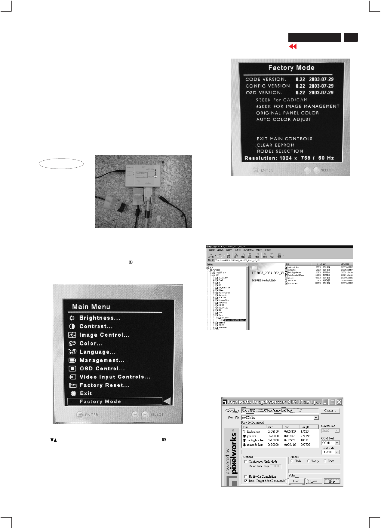
Firmware upgrade for CPU
Configuration and procedure
There is an application software to upgrade the firmware of CPU.
Bootcode of CPU should be embeded into CPU in production line
before you use those application (.exe) file.
Flashupgrader.exe => for Win95, 98 & ME
FlashupgraderNT.exe => for Win2000, NT & XP
CPU software=>Flashupgrader.exe or FlashupgraderNT.exe
I2C & RS232 Alignment KITs(3138 106 10198)
RS232 cable(9pins to 9pins) as below
Fig. 1 => Connection for Firmware upload.
** Do not connect Mains cord to Monitor at this moment. **
OPTIONAL TOOL
I2C & RS232 Alignment Kits --------------------->
(3138 106 10198)
9 pins to 9 pins cable --------------------->
Fig. 1
D-sub cable ----------------------------------------------->
Factory mode Adjustment:
HP L2035
Go to cover page
Fig. 3
Check Firmware version : example as below.
CODE VERSION. 0.22 2003-07-29
CONFIG VERSION. 0.22 2003-07-29
OSD VERSION. 0.22 2003-07-29
The updated firmware of CPU => as shown
in Fig. 4
1. Configdata.hex 2. Flasher.hex 3. Gui.hex 4. romcode.hex
Fig. 4
23
Entering factory mode as Press and button
simultaneously and power ON as Fig. 1shown below.
Menu auto
Execution files => as shown in Fig. 4
1.Make sure FlashUpgrader or FlashUpgraderNT is placed in the
same directory with *.hex files and pwSDK.ini
2.There two versions of FlashUpgraders for different Windows
operating systems.
Flashupgrader.exe => for Win95, 98 & ME
FlashupgraderNT.exe => for Win2000, NT & XP
3.
Remove the AC power cable
4. After double icon, you will see this
window:
clicking the FlashUpgrader
Use buttons to Factory Mode to enter by Menu then
appear Fig.2 TO SEE CODE VERSION as below
Page 24
24
HP L2035
Go to cover page
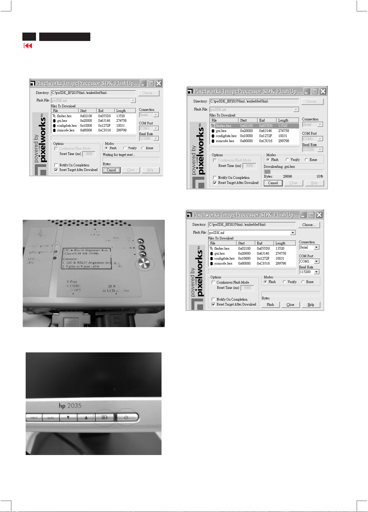
Firmware upgrade for CPU (Continued)
5. Make sure you choose the path of the files.
6. You will see the following screen
FlashUpgrader is waiting for the AC reset signal.
7.Make sure the I2C & RS232 switch (the circled button at the
right hand side of the following photo) of the communication box
is held down, the orange and the red LEDs light on while the other
green LED is off.
Then click Flash
9. Hold the two function keys and connect the AC cable.
The download progress should automatically start. When you see
a running progress bar like the diagram below, you may release
the two function keys.
10. When the download progress is completed, you may see the
FlashUpgrader like this:
Connect the box to the serial port of your PC via RS232 cable and
to the monitor via D-SUB cable.
8. Press the power and the menu key of the monitor at the same
The monitor will automatically be reset and you may confirm the
version number in the service menu.
PS. If the download does not start, reseting the power of the
communication box or restarting Windows may solve the
problem.
Page 25

Scalerboard function block of L2035
HP L2035
Go to cover page
Brightness
25
DVI-I
DVI-I
RG B
HV
D-SUB
IIC bus of EDID
EDID digital
DVI receiver
TMDS
THC63DV161
ADC
RG B HV
Multiplex
IIC bus of EDID
M24C02
AD9888KS-205
74LV4053
Flash memory
M29W800DT
Address bus A1~A19
Data bus D0~D15
2 pixel 8 bits data
bus & signal
IIC bus
2 pixel 8 bits data
bus & signal
ISP control
Scaler&
MCU
PW171
EEP ROM
M24C32
IIC bus
To DVI-RX
To ADC
To video decoder
DAC
& back light
control
M62334
+18V & +3.3V from power
& inverter board
+5V
+18v & 3v3
regulator
Power
To scaler chip
management
regulator and
To each block
switch to each
block
S-video
CVBS
EDID analog
M24C02
Video
decoder
SAA7115
RS-232
RS-232
port
IIC bus
YUV 16 bits & sync clk
Reset
LM8103X
Bus D0~D7
Buffer 74LVC541
8 bits data bus
& sync signal
8 bits data bus
& sync signal
LVDS TX
THC63LVDM83A
LVDS TX
THC63LVDM83A
Key pad & LED
Panel
inter-
face &
power
supply
Page 26

26
HP L2035
Go to cover page
Power board & inverter function block of L2035
AC inlet
& filter
AC 90 ~
240V
Rectifier
Power
stage
Controller
CPP, OPP
OVP
Regulation
feedback
Transformer
Low voltage
rectifier
+3.3V
regulator
+3V3 to
scalerboard
+18V to scaler
board and
inverter circuit
+18V
BL control
Brightness control
Power
switch &
regulator
Power stage
Full bridge &
transformer
Controller
CCFL X3
CCFL X3
Current
sense &
OVP/
Feed back/
Open lamp protect
OZ960G
feedback
Page 27

A
B
C
D
E
G
H
Schematic diagram(DVI/DSUB)
HP L2035
Go to cover page
3456
47K
2241
2223
8
7221
M24C02
3237
75R
645
7201
74LV4053PWT
1
2Y1
2
2Y0
3
3Y1
4
3Z
5
3Y0
6
E
7
VEE
8
GND
10p
DVI_A_VS
2242
100n
E0
E1
E2
SCL
WC_
1
1
1
3238
75R
16
VCC
1Y1
1Y0
10p
DVI_5V
+5V
1
2
3202
3
6
7
I017
I018
I019
+5V_DVI
15
2Z
14
1Z
13
12
11
S1
10
S2
9
S3
BAT54
6231
BAT54
6232
BAT54
6233
BAT54
6234
+5V
6226
BAT54
DSUB_HS DSUB_VS DVI_A_HS DVI_A_VS
4.8V
10K
6220
BAS32L
DSUB_B
DSUB_G
DSUB_R
3242
3247
3
F001
F002
F003
F004
1201
74320-1004
F005
F019
F020
100R3243
100R
100R
DVI_5V
DVI_SCL
DVI_SDA
DVI_5V
DVIVS
DVI_B
DVI_R
DVI_G
DVIHS
TXD_ISP
10K
ISP_SW
3225
0R
3228
F028
F029
F030
DSUB_VS
DSUB_HS
33p
F015
F016
F017
0R05
F023
F022
F006
F007
F008
F018
1
2
3
4
5
6
7
8
3244
3245
3246
0R
0R
5
4
3
2
1
I011
I012
2228
330p
RXC-
RXC+
RX0+
RX0-
RX1-
RX1+
RX2-
RX2+
F010
F011
F012
F014
100MHZ
5203
100MHZ5201
5202 100MHZ
+5V
2221
DSUB_SCL_ROM
+3.3V
3209 1K
3239
33p
2226
DSUB_SDA_ROM
1K
+5V_ESD
220n
2202
321475R
32192K2
2K2 3217
75R 3240
75R 3215
6218
BAS32L
6219
6227
BAV99
I013
2222
6225
BAT54
100n
+5V_ESD
BAV99
5221
100MHZ
100n
DSUB_CA
+5V_ESD +5V_ESD
6228
BAV99
100R
3216
I010
2201
BZX84-C5V1
3221
2224
6229
100R3218
10K
I016
I015
33p
6201
BAV99
6202
BAV99
DVI_A_VS
DVI_A_B
DVI_A_R
DVI_A_G
DVI_A_HS
2205
330p
+5V_ESD
220n
3222
2225
5222
5223
5224
+5V_ESD
6230
BAV99
2206
33p
10K
4.8V
33p
100MHZ
100MHZ
100MHZ
DVI_A_HS
I014
5
3236
75R
SDA
VSS
3226
VCC
4
1
2
A
SCALER PCB
SB: 58821 x2
PB: 58831
3203
1K
+3.3V
3204
+5V_ESD
2204
1K
F021
33p
F009
B
DVI_CA
C
D
6203
BAV99
7204
74LV4053PWT
1
6221
BAV99
6222
BAV99
6223
BAV99
2Y1
2
2Y0
3
3Y1
4
3Z
5
3Y0
6
E
7
VEE
8
GND
DSUB_SDA
F025
F026
F027
All rights reserved. Reproduction in whole or in parts
owner.
is prohibited without the written consent of the copyright
E
RXD_ISP
RXD
3220 1K
RXD_DDCCI
0R
3248
F
+5V_ESD
G
F
H
gedeeltelijk, is niet toegestaan dan met schriftelijke
toestemming van de auteursrechthebbende.
Alle rechten voorbehouden. Verveelvuldiging, geheel of
I
6224
BAV99
J
2K2
3212
17
18
19
20
21
22
23
24
VCC
1Y1
1Y0
3223
3224
DSUB_SCL
F024
F031
2K2
3229
2Z
1Z
S1
S2
S3
3230
3231
30
C6
100R
27
28
100R
15
14
13
12
11
31
9
10
11
12
13
14
15
16
C1
C3
C4
C2
32
16
15
14
13
12
11
10
DDCCI_SW
9
1221
17
16
100R
100R
25
29
C5
26
100n
2245
10
9
8
7
6
2227
EXCEPT 1201,1221 WERE CHIP COMPONENTS.
1
3
4
56
7
3205
0R
3208
2212
10u
2243
74HCT1G14GW
NC
INA
GND
EDID_SW
232270296001
3248
Ref Des WITHOUT_DDCCI
7
7
8
0R
3206
DVI_SDA
3207
100R
2213
330p
2244
7222
1
2
3
0R
DVI_SCL
100R
330p
+5V_DVI
220n
ADC5V
2229
VCC
5
OUTY
4
3232
0R05
3241
7226
MUN2211J
A_DSW
CHN SETNAME UH3 (HUD-3 / HPQ2035)
TYT12-
CLASS_NO
8
9
7202
M24C02
8
5
47K
Ref Des RESERVED
2231 223886775339
TMDS_HS
TMDS_VS
VCC
SDA
VSS
4
VCC
5
SDA
VSS
4
33p
33p
2233 223886775339
2235 223886775339
7223
74HCT1G14GW
NC
1
INA
2
GND
3
74LVC126AD
I021
I020
8
33p
33p
2237 223886775339
7227-A
2
1
5
5V
4
SCL
WC_
E0
E1
E2
SCL
WC_
10p
2241 223886715109
5
4
47K
3210
+5V_DVI
3211
7203
M24C02
10u
100n
2230
_DSUB_HS _DSUB_VS _DVI_A_HS
2231
33p
+3.3V
10K
DVI / DSUB
FJ6B2S/76
2003-08-27 3
NAME
Yikuan Yu/Sandy Yuan
CHECKMGr DATE
8
SUPERS.
******** 2003-08-27
9
910
11
6205
ESD0805A
RX0+
1
E0
2
E1
3
E2
6
7
1
2
3
6
7
223886715109
10p
2242
2243 222224119876
VCC
OUTY
3233
0R05
14
7
14
7
3213
223824615654
220n
10u
2244
ADC5V
2232
100n
3
6
7227-B
74LVC126AD
47K
3227
47K
3201
6235
10K
47K
3213 319802134730
3201 232270260103
3211 319802134730
2233
33p
+3.3V
2238
2
3200
10K
6236
BAS32L
47K
0R
3225 232270296001
74HCT1G14GW
NC
INA
GND
2.9V
100n
10K
BAS32L
EDID_SW
319802134730
3226
RX0-
RX1+
RX1-
DVI_R
DVI_G
DVI_B
232270296001
0R
47K
3242
7224
1
2
3
6213
ESD0805A
6214
ESD0805A
6215
ESD0805A
dio-esd0805a
3247 2322702960010R6205
VCC
5
OUTY
4
AHSOUT
AVSOUT
A_DSW
6206
6207
6208
ESD0805A
6206 dio-esd0805a
dio-esd0805a
6207
ADC5V
3234
0R05
I024
I025
3.3V
3138 158 5556
91
C
KONINKLIJKE PHILIPS ELECTRONICS N.V. 2000
10
11
ESD0805A
6208 dio-esd0805a
6209 dio-esd0805a
100n
2234
2.9V
3
11
12
6209
ESD0805A
RX2+
6210
RX2-
6211
RXC+
6212
RXC-
+5V_ESD
ESD0805A
ESD0805A
dio-esd0805a
6211 dio-esd0805a
6210
2235
33p
4
dio-esd0805a
ESD0805A
BAT54
BAT54
6214 dio-esd0805a
6215
6212 dio-esd0805a
6213 dio-esd0805a
6231 933742280215
6232 933742280215
7225
74HCT1G14GW
NC
5
1
INA
2
GND
4
3
9
10
12
13
8
14
7
14
7
13010 *** A3
74LVC126AD
11
7227-D
74LVC126AD
7227-C
12
6216
BAV99
6217
BAV99
BAT54
6233 933742280215
VCC
OUTY
I022
I023
1310
DVIHS
DVIVS
BAT54
BAS32L
6234 933742280215
6235 933913910115
7201 935174970118
ADC5V
2236
100n
_DVI_A_VS
3235
0R05
GHS
GVS
1
132
1212
74LV4053PWT
M24C02
7203 932214526668
2237
33p
--------
A
B
C
D
E
F
G
H
I
J
A
B
C
D
E
G
H
1201 A3
1221 F3
2201 D5
2202 A4
2204 C2
2205 C5
2206 C5
2212 B7
2213 B7
2221 E4
2222 E4
2223 E5
2224 F5
2225 F5
2226 G4
2227 H3
2228 H3
2229 E7
2230 E8
2231 E8
2232 E9
2233 E9
2234 E10
2235 E11
2236 E12
2237 E12
2238 F9
2241 D6
2242 D6
2243 D7
2244 D8
2245 D3
3200 A10
3201 B9
3202 F6
3203 B2
3204 B2
3205 B7
3206 B7
3207 B7
3208 B7
3209 F4
3210 A8
3211 B8
3212 H2
3213 B9
3214 C4
3215 C4
3216 C5
3217 C4
3218 C5
3219 C4
3220 D1
3221 E5
3222 E5
3223 F2
3224 F2
3225 F3
3226 C5
3227 A9
3228 G3
3229 H2
3230 H2
3231 H2
3232 E7
3233 E9
3234 E10
3235 E12
3236 G5
3237 G5
3238 G6
F
3239 G4
3240 C4
3241 F8
3242 F3
3243 D3
3244 E3
3245 E3
3246 E3
3247 F3
3248 E1
5201 C4
5202 C4
5203 C4
5221 E4
5222 G5
5223 G5
5224 G5
6201 A5
6202 A5
6203 C1
6205 A10
6206 A10
6207 A10
6208 B10
6209 A11
6210 A11
6211 A11
6212 B11
6213 B10
6214 B10
6215 C10
6216 B12
6217 B12
6218 D4
6219 D4
6220 F6
6221 E2
6222 F2
6223 G2
6224 H2
6225 E4
6226 E6
6227 F4
6228 H4
6229 H4
6230 H5
6231 D7
6232 D7
6233 D7
6234 D7
6235 C9
6236 C9
7201 B6
7202 A8
7203 B9
7204 D2
7221 F5
7222 E7
7223 E8
7224 E10
7225 E11
7226 F7
7227-A F9
7227-B G9
7227-C F11
7227-D G11
F001 A3
F002 A3
F003 A3
F004 A3
F005 A3
F006 B3
F007 B3
F008 B3
F009 C2
F010 B4
F011 B4
F012 B4
F014 C4
F015 C3
F016 C3
F017 C3
F018 C4
F019 B3
F020 B3
F021 B2
F022 G3
F023 G3
F024 G2
F025 F2
F026 G2
F027 G2
F028 G3
F029 G3
F030 G3
F031 G2
I010 D5
I011 H3
I012 H3
I013 E4
I014 E5
I015 F5
I016 F5
I017 G6
I018 G6
I019 G6
I020 G8
I021 F8
I022 F11
I023 G11
I024 F10
I025 G10
1 1601-3
1 V/div AC
2 mS/div
1 1601-2
1 V/div AC
2 mS/div
1 1601-1
1 V/div AC
2 mS/div
2 7602-6
0.5 V/div AC
5 mS/div
3 7602-9
0.5 V/div AC
5 uS/div
4 7602-12
0.5 V/div AC
5 mS/div
27
1
432
5
109876
11 12
Page 28

28
HP L2035
Go to cover page
Schematic diagram(ADC)
A
B
C
D
E
G
H
12345678910
26
AVDD1034AVDD1137AVDD1238AVDD13
AD9888KS-205
4
2
65
39
OVDD156OVDD269OVDD379OVDD489OVDD598OVDD6
7253
2258
6
47u
DVDD
GND2078GND21
68
5253
100MHZ
102
112
122
OVDD7
OVDD8
GND2299GND23
GND24
88
100
I030
GND25
101
2257
7
PVDD
52
PVDD147PVDD248PVDD3
DATACKB
SOGOUT
GND26
GND27
GND28
111
121
128
10u
7
ROUTA0
ROUTA1
ROUTA2
ROUTA3
ROUTA4
ROUTA5
ROUTA6
ROUTA7
ROUTB0
ROUTB1
ROUTB2
ROUTB3
ROUTB4
ROUTB5
ROUTB6
ROUTB7
GOUTA0
GOUTA1
GOUTA2
GOUTA3
GOUTA4
GOUTA5
GOUTA6
GOUTA7
GOUTB0
GOUTB1
GOUTB2
GOUTB3
GOUTB4
GOUTB5
GOUTB6
GOUTB7
BOUTA0
BOUTA1
BOUTA2
BOUTA3
BOUTA4
BOUTA5
BOUTA6
BOUTA7
BOUTB0
BOUTB1
BOUTB2
BOUTB3
BOUTB4
BOUTB5
BOUTB6
BOUTB7
DATACK
VSOUT
HSOUT
DVDD
8
DVDD
100n2275
2274 100n
120
AGRE0
119
AGRE1
118
AGRE2
117
AGRE3
116
AGRE4
115
AGRE5
114
AGRE6
113
AGRE7
110
AGRO0
109
AGRO1
108
AGRO2
107
AGRO3
106
AGRO4
105
AGRO5
104
AGRO6
103
AGRO7
97
AGGE0
96
AGGE1
95
AGGE2
94
AGGE3
93
AGGE4
92
AGGE5
91
AGGE6
90
AGGE7
87
AGGO0
86
AGGO1
85
AGGO2
84
AGGO3
83
AGGO4
82
AGGO5
81
AGGO6
80
AGGO7
77
AGBE0
76
AGBE1
75
AGBE2
74
AGBE3
73
AGBE4
72
AGBE5
71
AGBE6
70
AGBE7
64
AGBO0
63
AGBO1
62
AGBO2
61
AGBO3
60
AGBO4
59
AGBO5
58
AGBO6
57
AGBO7
I060
123
124
I057
127
I058
126
I059
125
CHN SETNAME UH3 (HUD-3 / HPQ2035)
CLASS_NO
2276 100n
3265 47R
47R3266
3267 47R
47R3268
TYT12-
100n2277
100n
2278
1.6V
1.8V
2V
2.1V
2.1V
1.6V
1.7V
0.7V
0.6V
0.8V
1.7V
1.2V
1.4V
1.3V
18
20
NI
2298
100n2280
2279 100n
I065
AGRE0
AGRE1
AGRE2
6
AGRE3
7
AGRO0
AGRO1
AGRO2
AGRO3
AGGE0
AGGE1
AGGE2
AGGE3
AGGO0
AGGO1
AGGO2
AGGO3
AGBE0
AGBE1
AGBE2
AGBE3
AGBO0
AGBO1
AGBO2
AGBO3
1
5
I066
2
I067
3
I068
45
2.1V
I073
1
8
I074
2
9
3
10
45
11
I081
12
1
I082
13
2
14
3
45
1.4V
I089
1
I090 I518
2
U95
3
I092
4
I097
1
1.2V
1.3V
2
I099
3
1.3V
45
1.8V
I105
1
1.8V
I106
2
1.4V
3
1.4V
I108
45
1.3V
1.6V
I064
2.9V
I063
NI
2p2
33p
2250
2281 100n
3269
3271
3273
3275
3277
3279
GCLK
AVSOUT
AHSOUT
GFBK
R
R
47R
R
R
R
R
47R
R
R
R
R
47R
R
R
R
R
47R
R
R
R
R
47R
R
R
R
R
47R
R
R
ADC
FJ6B2S/76
2003-08-27 3
Yikuan Yu/Sandy Yuan
NAME
CHECKMGr DATE
SUPERS.
******** 2003-08-27
98
109
PVDD
11
SCALER PCB
SB: 58821 x2
PB: 58831
I069
1
I070
2
3270
I071
3
I072
45
I077
1
2
3272
I079
3
I080
45
1
2
3274
3
I088
45
I093
1
I094
2
3276
I095
3
I096
45
1
I102
2
3278
I103
3
45
I109
1
I110
2
3280
I111
3
I112
45
NI
33p
223886775228
2p2
100MHZ
2422549434095255
100MHZ
2422549434095256
100MHZ
GRE0
GRE1
GRE2
GRE3
GRO0
GRO1
GRO2
GRO3
GGE0
GGE1
GGE2
GGE3
GGO0
GGO1
GGO2
GGO3
GBE0
GBE1
GBE2
GBE3
GBO0
GBO1
GBO2
GBO3
2283 100n
100n2284
AGRE4
AGRE5
AGRE6
AGRE7
AGRO4
AGRO5
AGRO6
AGRO7
AGGE4
AGGE5
AGGE6
AGGE7
AGGO4
AGGO5
AGGO6
AGGO7
AGBE4
AGBE5
AGBE6
AGBE7
AGBO4
AGBO5
AGBO6
AGBO7
Ref Des
2250 223886775339
2298
5254 242254943409
100n2282
I113
8
I114
7
5206
6
I116
I121
8
I122
7
I123
6
I124
I129
8
I529
7
I530
6
I531
I517
8
7
I519
6
I520
5
I521
8
I522
7
I523
6
I524
I525
8
I526
7
I527
6
I528
19
17
3138 158 5556
92
C
KONINKLIJKE PHILIPS ELECTRONICS N.V. 2000
10
123
AVDD
4
A
3251
15
AVDD
PVDD
100n2272
100n
2271
I032
I035
I036
1n2292
47n2294
47n2295
47n2297
2273 100n
3K3
50
FILT
2
REF_BYPASS
9
RMIDSCV
24
BMIDSCV
31
SDA
32
SCL
33
A0
I039
29
CKINV
I040
30
53
CLAMP
I041
54
COAST
I042
CKEXT
45
HSYNC0
44
VSYNC0
5
RAIN0
13
GAIN0
I045
12
SOGIN0
20
BAIN0
43
HSYNC1
42
VSYNC1
8
RAIN1
17
GAIN1
I052
16
SOGIN1
23
BAIN1
GND1
3
4
ADC5V
4 132
AVDD
1
10
AVDD1
AVDD514AVDD618AVDD721AVDD825AVDD9
AVDD26AVDD37AVDD4
GND315GND419GND522GND627GND728GND835GND9
GND2
11
100MHZ
7254
LM2937IMP-3.3
1
2249
100n
5
GND1040GND1141GND1246GND1349GND1451GND1555GND1665GND1766GND1867GND19
36
5256
Vi3Vo
GND
100n2261
2262 100n
100n2263
2264 100n
2265 100n
100n2266
2267 100n
100n2268
100n2269
100n2270
B
PVDD
C
7251
Vi1Vo
Vin2Vout
5254
100MHZ
4
GND
5255
100MHZ
GND
2
3
SDA
SCL
GHSFOUT
GBLKSPL
GCOAST
_DVI_A_HS
_DVI_A_VS
DVI_A_R
DVI_A_G
DVI_A_B
_DSUB_HS
_DSUB_VS
DSUB_R
DSUB_G
DSUB_B
3
7252
LM3480IM3-3.3
1
DVDD
0R053257
0R053258
0R053260 2293 47n
3261 0R05
3262 0R05
3264 0R05
I026
2253
I028 I029
2256
D
All rights reserved. Reproduction in whole or in parts
is prohibited without the written consent of the copyright
owner.
E
F
G
F
H
gedeeltelijk, is niet toegestaan dan met schriftelijke
Alle rechten voorbehouden. Verveelvuldiging, geheel of
toestemming van de auteursrechthebbende.
ADC5V
LM2937IMP-3.3
2251
100n
I
ADC5V
2254
J J
100n
2289 100n
3252 100R
3253 100R
3254 10K
3255 10K
5251
100MHZ
47u
5252
100MHZ
47u
I027
2252
2255
0R053263
I047
I048
I049
100n2287
100n2288
10K3256
4.2V
I055
I056
3.2V
39n2285
2286 3n9
2290 47n
2291 47n
3.7V
2296 1n
10u
10u
3
11 12
12
I117
GRE4
8
R
I118
GRE5
7
R
47R
I119
GRE6
6
R
I120
R
R
R
47R
R
R
R
R
47R
R
R
R
R
47R
R
R
R
R
47R
R
R
R
R
47R
R
R
GRE7
I125
GRO4
8
I126
GRO5
7
I127
GRO6
6
I128
GRO7
I532
GGE4
8
I533
GGE5
7
I534
GGE6
6
I535
GGE7
I536
GGO4
8
I537
GGO5
7
I538
GGO6
6
I539
GGO7
I542
GBE4
8
I543
GBE5
7
I544
GBE6
6
I545
GBE7
I546
GBO4
8
I547
GBO5
7
I548
GBO6
6
I549
GBO7
13010 ***
12111
1
13
--------
A
B
C
D
E
F
G
H
I
A3
G
2249 H5
2250 G8
2251 G2
2252 G3
2253 G3
2254 H2
2255 H3
2256 H3
2257 H6
2258 H6
2261 A2
2262 A2
2263 A2
A
2264 A2
2265 A3
2266 A3
2267 A3
2268 A3
2269 A4
2270 A4
2271 A4
2272 A4
2273 A4
2274 A7
2275 A7
B
2276 A8
2277 A8
2278 A8
2279 A8
2280 A8
2281 A9
2282 A9
2283 A9
2284 A10
2285 B3
2286 C4
C
2287 C3
2288 C3
2289 C3
2290 E4
2291 E4
2292 E4
2293 E4
2294 E4
2295 E4
2296 F4
2297 F4
2298 G8
D
3251 B4
3252 C3
3253 C3
3254 D3
3255 D3
3256 D3
3257 E3
3258 E3
3260 E3
3261 E3
3262 E3
3263 D3
E
3264 F3
3265 F7
3266 F7
3267 F7
3268 F7
3269 B9
3270 B10
3271 C9
3272 C10
3273 C9
3274 C10
F
3275 D9
3276 D10
3277 E9
3278 E10
3279 E9
3280 E10
5206 B9
5251 F3
5252 H3
5253 H6
5254 F3
5255 G3
5256 G5
7251 F3
7252 G3
7253 D6
7254 G5
I026 F3
I027 F4
I028 H3
I029 H3
I030 H6
I032 C4
I035 C4
H
I036 C4
I039 D4
I040 D4
I041 D4
I042 D4
I045 E4
I047 E4
I048 E4
I049 E4
I052 E4
I055 E4
I056 F4
I057 F7
I058 F7
I059 F7
I060 F7
I063 F8
I064 F8
I065 B8
I066 B8
I067 B8
I068 B8
I069 B10
I070 B10
I071 B10
I072 B10
I073 C8
I074 C8
I077 C1
I079 C10
I080 C1
I081 C8
I082 C8
I088 D10
I089 D8
I090 D8
I092 D8
I093 D1
I094 D10
I095 D10
I096 D10
I097 D8
I099 E8
I102 E10
I103 E10
I105 E8
I106 E8
I108 F8
I109 E1
I110 E10
I111 E1 0
I112 F10
I113 B9
I114 B9
I116 B9
I117 B1
I118 B11
I119 B11
I120 B11
I121 C9
I122 C9
I123 C9
I124 C9
I125 C1
I126 C11
I127 C11
I128 C11
I129 C9
I517 D9
I518 D9
I519 D9
I520 D9
I521 D9
I522 E9
I523 E9
I524 E9
I525 E9
I526 E9
I527 E9
I528 F9
I529 C9
I530 C9
I531 D9
I532 C1
I533 C11
I534 C11
I535 D11
I536 D11
I537 D11
I538 D11
I539 D11
I542 D11
I543 E11
I544 E11
I545 E11
I546 E11
I547 E11
I548 E11
I549 F11
IXXX D8
0
0
0
0
1
1
1
5 3269-1 12 3273-1
0.5 V/div AC
10 uS/div
0.5 V/div AC
10 uS/div
6 3269-3 13 3273-2
0.5 V/div AC
5 mS/div
0.5 V/div AC
10 uS/div
7 3269-4 14 3273-3
0.5 V/div AC
5 mS/div
8 3271-1
0.5 V/div AC
5 mS/div
9 3271-2
0.5 V/div AC
5 mS/div
10 3271-3
0.5 V/div AC
10 uS/div
11 3271-4
0.5 V/div AC
10 uS/div
19 7253-126
0.5 V/div AC
10 uS/div
0.5 V/div AC
10 uS/div
15 7253-42
0.5 V/div AC
5 mS/div
16 7253-43
0.5 V/div AC
5 uS/div
17 7253-125
0.5 V/div AC
5 uS/div
18 7253-123
0.5 V/div AC
20 mS/div
20 7253-127
0.5 V/div AC
5 mS/div
1234567891011
12
Page 29

A
B
C
D
G
H
Schematic diagram(TMSD RX)
HP L2035
Go to cover page
7
1
254
3
6
7
8
89
9
10 11
11 1210
12123456
13
SCALER PCB
TMDSRX5V
7305
2326
3324
0R05
100n
TMDS_VS
NI
2328
33p
VCC
5
OUTY
4
GBE0
6
GBE1
7
GBE2
8
GBE3
GGE0
6
GGE1
7
GGE2
8
GGE3
GRE0
6
GRE1
7
GRE2
8
GRE3
GBO0
6
GBO1
7
GBO2
8
GBO3
GGO0
6
GGO1
7
GGO2
8
GGO3
GRO0
6
GRO1
7
GRO2
8
GRO3
74HCT1G14GW
NC
1
INA
2
GND
3
45
PGBE4
3
PGBE5
PGBE6
PGBE7
PGGE4
PGGE5
PGGE6
PGGE7
PGRE4
PGRE5
PGRE6
PGRE7
PGBO4
PGBO5
PGBO6
PGBO7
PGGO4
PGGO5
PGGO6
PGGO7
PGRO4
PGRO5
PGRO6
PGRO7
3311
2
1
45
3
3313
2
1
45
3
3315
2
1
45
3
3317
2
1
45
3
3319
2
1
45
3
3321
2
1
LM2937IMP-3.3
2313
100n
2320
100n
SB: 58821 x2
PB: 58831
AVCC
2301 470p
5305
100MHZ
7302
4
Vi1Vo
GND
5306
100MHZ
7303
LM3480IM3-3.3
2
Vin1Vout
GND
3
470p2302
2303 470p
Ref Des NI
2324 223886775228
2328
2329 223886775339
3305 232270296001
3322
5305 242254943409
5306 242254943409
3
2
I430
470p2304
2p2
223886775339
33p
33p
0R
319802131030
10K
100MHZ
100MHZ
I076
47u
2316
47u
2322
OVCC
5301
100MHZ
5302
100MHZ
5303
100MHZ
5304
100MHZ
470p2305
2306 470p
2318
2315
2314
2321
I431
I429
I416
10u
I415
10u
10u
10u
470p2307
2308 470p
2309 470p
_TMDSRXPD
OVCC
CVCC
AVCC
PVCC
OVCC
CVCC
470p2310
AVCC
I062
2317
2311 470p
100n
SCDT
RX2RX2+
RX1RX1+
RX0RX0+
RXC+
RXC-
470p2312
3301
3323
0R05
3302
3305
I075
510R
OVCC
3322
10K
0R
NI
I051
NI
I061
3310
3312
3314
3316
3318
3320
7304
74HCT1G14GW
NC
1
INA
2
GND
3
R
R
47R
R
R
R
R
47R
R
R
R
R
47R
R
R
R
R
47R
R
R
R
R
47R
R
R
R
R
47R
R
R
OVCC
AVCC
95
AVCC182AVCC284AVCC388AVCC4
96
EXT_RES
9
PDO
81
RX2-
80
RX2+
86
RX1-
85
RX1+
91
RX0-
90
RX0+
93
RXC+
94
RXC-
10K
2
PD
100
OCK_INV
4
PIXS
7
STAG_OUT
99
RSVD
1
DFO
3
ST
AGND179AGND283AGND387AGND489AGND5
OVCC118OVCC229OVCC343OVCC457OVCC5
THC63DV161
OGND119OGND2
92
28
7301
OGND345OGND458OGND5
78
76
CVCC
VCC16VCC3
PVCC
38
67
TOUT
TEST
GND15GND3
68
39
97
PVCC
PGND
98
2323
100n
SCDT
ODCK
VSYNC
HSYNC
B10
B11
B12
B13
B14
B15
B16
B17
G10
G11
G12
G13
G14
G15
G16
G17
R10
R11
R12
R13
R14
R15
R16
R17
B20
B21
B22
B23
B24
B25
B26
B27
G20
G21
G22
G23
G24
G25
G26
G27
R20
R21
R22
R23
R24
R25
R26
R27
CT1
CT2
CT3
2324
GFBK
I078
SCDT
GCLK
I083
GPEN
NI
2p2
45
PGBE0
3
PGBE1
2
PGBE2
1
PGBE3
45
PGGE0
3
PGGE1
2
PGGE2
1
PGGE3
45
PGRE0
3
PGRE1
2
PGRE2
1
45
PGBO0
3
PGBO1
2
PGBO2
1
PGBO3
45
PGGO0
3
PGGO1
2
PGGO2
1
PGGO3
45
PGRO0
3
PGRO1
2
PGRO2
1
PGRO3
UH3 (HUD-3 / HPQ2035)SETNAMECHN
3308 47R
8
44
46
DE
47
48
10
I085
11
I086
12
I087
13
I098
14
I100
15
I101
16
I432
17
I433
20
I434
21
I435
22
I436
23
I437
24
25
26
I438
27
I439
30
31
32
33
I440
34
35
I442
36
I443
37
I444
49
I445
50
I446
51
I447
52
I448
53
I449
54
I450
55
I451
56
I452
59
I453
60
I454
61
62
63
64
65
I455
66
I456
69
I457
70
I458
71
I459
72
I460
73
I461
74
I462
75
I463
77
40
41
42
CLASS_NO
3327 47R
PGBE0
PGBE1
PGBE2
PGBE3
PGBE4
PGBE5
PGBE6
PGBE7
PGGE0
PGGE1
PGGE2
PGGE3
PGGE4
PGGE5
PGGE6
PGGE7
PGRE0
PGRE1
PGRE2
PGRE3
PGRE4
PGRE5
PGRE6
PGRE7
PGBO0
PGBO1
PGBO2
PGBO3
PGBO4
PGBO5
PGBO6
PGBO7
PGGO0
PGGO1
PGGO2
PGGO3
PGGO4
PGGO5
PGGO6
PGGO7
PGRO0
PGRO1
PGRO2
PGRO3
PGRO4
PGRO5
PGRO6
PGRO7
TYT12-
47R3309
A
B
C
D
All rights reserved. Reproduction in whole or in parts
is prohibited without the written consent of the copyright
owner.
E
F
E
G
TMDSRX5V
F
H
gedeeltelijk, is niet toegestaan dan met schriftelijke
toestemming van de auteursrechthebbende.
Alle rechten voorbehouden. Verveelvuldiging, geheel of
TMDSRX5V
I
TMDSRX5V
2327
3325
0R05
100n
TMDS_HS
2329
NI
33p
VCC
5
OUTY
4
A
A
B
B
C
47R
47R
47R
47R
47R
47R
GBE4
6
GBE5
7
GBE6
8
GBE7
GGE4
6
GGE5
7
GGE6
8
GGE7
GRE4
6
GRE5
7
GRE6
8
GRE7PGRE3
GBO4
6
GBO5
7
GBO6
8
GBO7
GGO4
6
GGO5
7
GGO6
8
GGO7
D
E
F
G
C
D
E
F
GRO4
6
GRO5
7
GRO6
8
GRO7
H
R
R
R
R
R
R
R
R
R
R
R
R
R
R
R
R
R
R
R
R
R
R
R
R
G
I
--------
1
TMDS RX
J
2003-08-27
Yikuan Yu/Sandy Yuan
NAME
1
2
34 5
6
7
810
3
FJ6B2S/76
SUPERS.
2003-08-27********
DATEMGr CHECK
91112
3138 158 5556
C
KONINKLIJKE PHILIPS ELECTRONICS N.V. 2000
J
H
39
***10 130
A3
13
2301 B2
2302 B2
2303 B2
2304 B3
2305 B3
2306 B3
2307 B3
2308 B4
2309 B4
2310 B4
2311 B5
2312 B5
2313 F2
2314 F3
2315 E3
2316 F3
2317 E4
2318 E3
2320 G2
2321 G3
2322 G3
2323 B7
2324 C8
2326 A10
2327 A11
2328 B10
2329 B11
3301 B5
3302 E5
3305 E5
3308 B7
3309 B7
3310 C9
3311 C11
3312 D9
3313 D11
3314 D9
3315 D11
3316 E9
3317 E11
3318 F9
3319 F11
3320 F9
3321 F11
3322 D5
3323 D5
3324 B10
3325 B11
3327 B7
5301 E3
5302 E3
5303 F3
5304 G3
5305 E2
5306 F2
7205 E2
7301 D6
7303 G2
7304 A9
7305 A11
I051 B5
I061 D5
I062 D4
I075 E5
I076 E3
I078 B8
I083 B8
I085 C7
I086 C7
I087 C7
I098 C7
I100 C7
I101 C7
I415 E3
I416 F3
I429 E3
I430 G2
I431 G3
I432 C7
I433 C7
I434 C7
I435 C7
I436 C7
I437 C7
I438 D7
I439 D7
I440 D7
I442 D7
I443 D7
I444 D7
I445 D7
I446 E7
I447 E7
I448 E7
I449 E7
I450 E7
I451 E7
I452 E7
I453 E7
I454 E7
I455 F7
I456 F7
I457 F7
I458 F7
I459 F
I460 F7
I461 F7
I462 F7
I463 F7
29
7
321
54
67
8 9 10 11 12
Page 30

30
HP L2035
Go to cover page
A
B
C
D
All rights reserved. Reproduction in whole or in parts
is prohibited without the written consent of the copyright
E
F
gedeeltelijk, is niet toegestaan dan met schriftelijke
Alle rechten voorbehouden. Verveelvuldiging, geheel of
G
H
Schematic diagram(LVDS TX)
123456789101112
12 13
TO PANEL
60934
U79
FXXX
SR0M
SR0P
SR1M
SR1P
SR2M
SR2P
SR3M
SR3P
U80
FR3M
FR3P
U81
31 32
U34
U35
U36
U37
U38
U39
U40
U41
U42
U43
U44
U45
U46
U47
U48
U49
U50
U51
U52
U53
1
LCM18V
49
2533
SCLKINM
SCLKINP
100n
FR0M
FR0P
FR1M
FR1P
FR2M
FR2P
FCLKINM
FCLKINP
13
1501
30
29
28
27
26
25
24
23
22
21
20
19
18
17
16
15
14
13
12
11
10
9
8
7
6
5
4
3
2
1
--------
A
B
C
D
E
F
G
H
I
J
A3***10 130
A
B
C
D
owner.
E
F
G
H
toestemming van de auteursrechthebbende.
I
J
1
SCALER PCB
2501
100n
100n
2502
2521
100n
100n
2527
1
2
SB: 58821 x2
PB: 58831
2503
100n
2504
100n
+3.3V_LVDS
5521
100MHZ
U77
10u
2523
2522
100n
+3.3V_LVDS
5523
100MHZ
U76
10u
100n
2529
2528
2
3501
2R2
2505
100n
2506
+3.3_LVDS_OD
+3.3_PLL_OD
543
+3.3V_LVDS+3.3V
5501
100MHZ
+3.3_TTL_OD
100n
2507
10u
2511
100n
2513
100n
2512
2524
2530
100n
100n
100n
+3.3V_LVDS
2525
100n
+3.3V_LVDS
100n
2531
2514
5522
2526
5524
2532
100n
10u
10u
2515
100MHZ
U22
+3.3_LVDS_EV
100MHZ
U78
+3.3_PLL_EV
100n
+3.3V_LVDS
2516
100n
3541
5511
2517
U10
10u
100MHZ
+3.3_TTL_EV
NIRef Des
232270296001
0R
2322702960013544
0R
+3.3_TTL_EV
3541
NI
3542
+3.3_TTL_EV
U74
1
U12
PEV_R7
+3.3_TTL_EV
PEV_R5
PEV_G0
PEV_G1 PEV_R0
PEV_G2
PEV_G6
PEV_G7
+3.3_TTL_EV
PEV_G3
PEV_G4
PEV_G5
PEV_B0
0R
PEV_B6
PEV_B7
PEV_B1
0R05
PEV_B2
PEV_B3
PEV_B4
PEV_B5
3543
10K
LVDS_HS
LVDS_VS
LVDS_SW
2
U14
3
U15
4
5
U25
6
7
8
9
U26
10
11
12
13
U27 U28
14
15
16
U21
17
18
19
20
21
22
23
24
U75
25
26
U23
27
U24
28
Vcc0
TD1
TA5
TA6
GND0
TB0
TB1
TD2
Vcc1
TD3
TB2
TB3
GND1
TB4
TB5
TD4
R_F
TD5
TB6
TC0
GND2
TC1
TC2
TC3
TD6
Vcc2
TC4
TC5
7
7501
THC63LVDM83A
TA4
TA3
TA2
GND4
TA1
TA0
TD0
LVDSGND2
TA+
TB+
LVDSVcc
LVDSGND1
TC+
TCLK-
TCLK+
TD+
LVDSGND0
PLLGND1
PLLVcc
PLLGND0
PDWN
CLKIN
TC6
GND3
TA-
TB-
TC-
TD-
CLASS_NO
PEV_R4
56
PEV_R3
55
PEV_R2
54
53
PEV_R1
52
51
PEV_R6
50
49
SR0M
48
47
SR0P
SR1M
46
SR1P
45
+3.3_LVDS_EV
44
43
SR2M
42
41
SR2P
SCLKINM
40
SCLKINP
39
38
SR3M
SR3P
37
36
35
+3.3_PLL_EV
34
33
32
PANEL_CLK
31
LVDS_EN
30
29
TYT12-
910
U11
1
Vcc0
U16
+3.3_TTL_OD
3544
NI
3546
+3.3_TTL_OD
0R
0R05
POD_R7
+3.3_TTL_OD
POD_R5
POD_G0
POD_G1
POD_G2
POD_G6
POD_G7
+3.3_TTL_OD
POD_G3
POD_G4
POD_G5
POD_B0
POD_B6
POD_B7
POD_B1
POD_B2
POD_B3
POD_B4
POD_B5
3545
10K
LVDS_HS
LVDS_VS
2
TD1
U17
3
TA5
U18
4
TA6
5
GND0
U30
6
TB0
7
TB1
8
TD2
9
Vcc1
U29
10
TD3
11
TB2
12
TB3
13
GND1
14
TB4
15
TB5
16
TD4
U20
17
R_F
18
TD5
19
TB6
20
TC0
21
GND2
22
TC1
23
TC2
24
TC3
U19
25
TD6
26
Vcc2
27
TC4
28
TC5
UH3 (HUD-3 / HPQ2035)SETNAMECHN
7502
THC63LVDM83A
GND4
TD0
LVDSGND2
LVDSVcc
LVDSGND1
TC+
TCLK-
TCLK+
TD+
LVDSGND0
PLLGND1
PLLVcc
PLLGND0
PDWN
CLKIN
TC6
GND3
TA4
TA3
TA2
TA1
TA0
TA+
TB+
TC-
TD-
1186
POD_R4
56
POD_R3
55
POD_R2
54
53
POD_R1
52
POD_R0
51
POD_R6
50
49
FR0M
48
TA-
47
FR0P
FR1M
46
TB-
45
FR1P
+3.3_LVDS_OD
44
43
FR2M
42
41
FR2P
FCLKINM
40
39
FCLKINP
38
FR3M
FR3P
37
36
35
+3.3_PLL_OD
34
33
32
PANEL_CLK
31
LVDS_EN
30
29
LVDS TX
3138 158 5556
32003-08-27
Yikuan Yu/Sandy Yuan
NAME
3
7
MGr CHECK
8
FJ6B2S/76
SUPERS.
DATE
2003-08-27********
C
KONINKLIJKE PHILIPS ELECTRONICS N.V. 2000
109654
11 12
A
B
C
D
E
F
G
H
U10 B5
U10 B6
U11 B9
U12 B6
U14 B6
U15 B6
U16 B9
U17 B9
U18 B9
U19 E9
U20 D9
U21 D6
U22 C2
U22 E2
U22 C4
U22 E4
U22 E6
U23 E6
U24 F6
U25 B6
U26 C6
U27 D6
U28 D9
U29 C9
U30 B9
U34 B12
U35 B12
U36 C12
U37 C12
U38 C12
U39 C12
U40 C12
U41 C12
U42 C12
U43 D12
U44 D12
U45 D12
U46 D12
U47 D12
U48 E12
U49 E12
U50 E12
U51 E12
U52 E12
U53 E12
U79 A11
U80 F12
U81 D12
1501 D12
2501 B2
2502 B2
2503 B2
2504 B2
2505 B2
2506 B3
2507 B3
2511 B3
2512 B4
2513 B4
2514 B4
2515 B4
2516 B5
2517 B5
2521 D2
2522 D2
2523 D2
2524 D4
2525 D4
2526 D4
2527 E2
2528 E2
2529 E2
2530 E4
2531 E4
2532 E4
2533 B11
3501 B3
3541 D5
3542 D5
3543 E6
3544 D8
3545 E9
3546 D8
5501 B3
5511 B5
5521 C2
5522 C4
5523 E2
5524 E4
7501 D7
7502 D10
FXXX D12
1234
56789101112
Page 31

A
B
C
D
E
G
H
Schematic diagram(SCALER Pw171)
HP L2035
Go to cover page
1234
4
POD_B2
POD_B1
POD_B3
6
7
100R
R
3403
45
DBOI1
DBOI2
DBOI3
D0
SCDT
SLEEPLED
I351
I352
I353
I354
A3
H2
D0H3D1
PORTA5B3PORTA6A2PORTA7
RESET
UCSRC
MCKEXT
WDTEN
DCKEXT
CLKIN
F4
E1
Y3
Y2
AF15
AE15
I367
I366
I380
I381
RESET
MCKEXT
WDTEN
DCKEXT
0R
3417
100n2419
100n2418
2420 100n
POD_B6
POD_B5
POD_B4
6
7
8
100R
RRR
3404
123
DBOI4
DBOI5
DBOI6
D9D8D7D6D5D4D3D2D1
I346
I347
I350
I349
I344
I348
I345
L4
D2J4D3J3D4K1D5K2D6L1D7L2D8L3D9
RXDD1TXD
IRRCVR0E3IRRCVR1
XTAL_I
XTAL_O
Y4
100n2421
D2
I368
TXD
RXD
IRRCVR0
1401
10p2433
14M31818HZ
100n
2422
E2
100n2423
CPUEN
F2
+3.3V
2424 100n
D10
I343
A14
VUV0
A
B
SCALER PCB
SB: 58821 x2
12
+3.3V_S
100n
2451
100n
2452
100n
2453
100n
2454
100n
2455
ADCPW
VIDEOPW
TMDSRXPW
I364
I363
I365
100n
2456
LVDS_SW
LCDPW
I362
I361
A7
100n
100n
2457
2458
VIDEOLED
PCLED
AUDIOPW
U3
I359
I360
C9
100n
100n
2459
2460
_EEWR
VIDEO_CE
EDID_SW
I357
A_DSW
100n
2438
ISP_SW
MUTEOUT
I355
I356
3
+3.3V
100n
34013K3
2439
POWERLED
DSUB_CA
SDA
B6
3402
DVI_CA
SCL
POD_B0
8
RRR
123
3K3
DBOI0
DCSW1
MUTEIN
_TMDSRXPD
U2
D5
PB: 58831
PORTB0C5PORTB1D6PORTB2B4PORTB3A4PORTB4C6PORTB5B5PORTB6A5PORTB7
PORTC5B8PORTC6D9PORTC7
AF9
AF5
AF3
AC7
AC4
AB1
AA4
Y23
W26
U23
N25
N23
M23
K23
H24
G23
D23
D20
D17
D13
D10
B24
B20
B19
A19
A18
A17
0R053421
D3
Y1
U4
P4
M2
K4
J2
G4
D7
D4
A1
10K3419
100n2404
VSS55
VSS54
VSS53
VSS52
VSS51
VSS50
VSS49
VSS48
VSS47
VSS46
VSS45
VSS44
VSS43
VSS42
VSS41
VSS40
VSS39
VSS38
VSS37
VSS36
VSS35
VSS34
VSS33
VSS32
VSS31
VSS30
VSS29
VSS28
VSS27
VSS26
VSS25
VSS24
VSS23
VSS22
VSS21
VSS20
VSS19
VSS18
VSS17
VSS16
VSS15
VSS14
VSS13
VSS12
VSS11
VSS10
VSS9
VSS8
VSS7
VSS6
VSS5
VSS4
VSS3
VSS2
VSS1
VSS0
A8
I370
34220R05
2405 100n
MODE1
MODE2
E4
AC5
I372
I371
342410K
0R05 3423
100n2406
PORTC0A6PORTC1D8PORTC2C8PORTC3B7PORTC4
MODE0
CPUTCLK
CPUTDI
CPUTDO
B9
AF2
AE4
TDO
TDI
TCK
100n2407
2408 100n
NMI
EXTINT0G2EXTINT1G1EXTINT2
CPU_TMS
F1
H1
B17
I373
NMI
TMS
3418
4K7
Ref Des RESERVED
2462 223886715109
3422 319802190030
3428 232270260229
100n2411
100n2409
2410 100n
CS0R3CS1R4CS2T1CS3
I374
_CS0
+3.3V
10p
0R05
22R
2412 100n
AF22
AF21
AF20
AF16
AE26
AE25
AE20
AE14
AD22
AC23
AC20
AC18
AC17
AC14
AC13
AC11
AC10
AB25
All rights reserved. Reproduction in whole or in parts
is prohibited without the written consent of the copyright
owner.
C
D
E
F
G
F
H
+3.3V
gedeeltelijk, is niet toegestaan dan met schriftelijke
Alle rechten voorbehouden. Verveelvuldiging, geheel of
toestemming van de auteursrechthebbende.
3420 10K
I
+2.5V
J
10u
100n
2401
2402
2403 100n
1
RAMOE
RAMWEP1RD
ROMWE
T2
P2
R2
R1
I376
I377
I375
_ROMWE
_ROMOE
+3.3V
100n2413
2415 100n
2414 100n
3
PORTA0C1PORTA1C2PORTA2B1PORTA3B2PORTA4
ROMOE
WR
BHEN
T3
T4
U1
_BHEN
100n2416
I378
100n
2417
3416
10K
F3
I379
56789101112
5
POD_B7
POD_G0
5
8
R
RRR
4
123
DBOI7
DGOI0
D15
D14
D13
D12
D11
I339
I340
I338
I342
I341
N4
D10M3D11M4D12N1D13N2D14N3D15
VB2
VB3
VB4
VB5
VB0
VB1
B15
A15
D15
C15
D16
VUV5
VUV4
VUV3
VUV2
VUV1
PANEL_CLK
10p
2432
POD_G3
POD_G2
POD_G1
6
7
100R
R
3405
45
DGOI1
DGOI2
DGOI3
A4A3A2A1A0
I335
I334
I337
I332
I333
I336
V1
A0U2A1
A2V2A3W1A4V3A5V4A6W3A7W4A8
VB6
VB7
VG0
VG1
VG2
A16
B12
A12
VUV7
C12
VY0
VY1
3427
VY2
B13
VY3
470R
C16
VUV6
POD_G5
POD_G4
7
8
RRR
123
DGOI4
DGOI5
I331
I330
I329
AA1
VG3
VG4
VG5
A13
D14
C14
VY6
VY5
VY4
2461
POD_R0
POD_G7
POD_G6
8
6
100R
RRR
R
3406
A9A8A7A6A5
I328
AB2
VG6
B14
VY7
123
45
DROI0
DGOI6
DGOI7
A16
A15
A14
A13
A12
A11
A10
I325
I326
I327
I323
I322
I321
I324
AA3
AB3
AE1
AB4
AC1
AD1
AD2
A9
A10
A11
A12
A13
A14
A15
VR3
3428
VR0A9VR1
B10
5401
BLM21
VR4
VR2
B11
A10
D11
C11
22R
VG7
10p
7
POD_R3
POD_R2
POD_R1
6
7
100R
R
3407
45
DROI1
DROI2
DROI3
A19
A18
A17
I320
I318
I319
AF1
AE2
AC3
A16
VR5
A11
A17
A18
A19
7401
PW171B-20U
VR6
VR7
D12
C21
VFIELD
10p
2462
AD16
AC16
DENB
VFIELD
VHS
A22
B21
VVS
DCLK
AF17
DENG
VVS
A21
VHS
POD_R5
POD_R4
LVDS_EN
I317
7
8
RRR
123
DCLK
I315
AD15
AC15
DVS
DHS
DENR
VLAV
VPEN
VCLK
B18
B16
VPEN
VCLK
LVDS_VS
LVDS_HS
6
100R
R
3425
45
DBOI3
DBOI2
DBOI1
DBOI0
I314
I311
AF6
AE7
AE6
AC6
AD13
DBO0
DBO1
DBO2
DCLK_OUT
GBO0
GBO1
GBO2
GBO3
B22
A23
B23
D21
C22
GBO0
GBO4
GBO3
GBO2
GBO1
8
RRR
123
DROI4
DBOI4
DBOI5
I310
AE5
AD5
DBO3
DBO4
GBO4
GBO5
D22
C23
GBO6
GBO5
DBOI6
I308
AF4
DBO5
GBO6
A24
GBO7
7
DROI5
DBOI7
I307
AE3
DBO6
GBO7
3408
DBO7
F23
GGO0
POD_R6
6
100R
DROI6
DGOI0
AF10
DGO0
GGO0
GGO1
D25
GGO1
EXCEPT 4401 WERE CHIP COMPONENTS.
TYT12-
+3.3V_S
CLASS_NO
PEV_B1
PEV_B2
PEV_B0
POD_R7
8
RRR
R
45
123
DBEI0
DROI7
DGOI3
DGOI2
DGOI4
DGOI1
DGOI5
I303
I305
I304
I302
I301
AE9
AD8
AC8
AD9
AC9
DGO3
DGO4
DGO1
DGO2
GGO2
GGO3
GGO4
GGO5
F24
F25
E25
E26
D26
GGO6
GGO5
GGO4
GGO3
GGO2
PEV_B3
6
7
100R
R
3409
45
DBEI1
DBEI2
DBEI3
DROI0
DROI1
DGOI6
DGOI7
I297
I296
I295
I298
I300
AF8
AF7
AF13
AC12
AD12
DRO1
DRO0
DGO5
DGO6
DGO7
GRO0
GRO1
GRO2
GGO6
GGO7
T23
F26
R24
R25
R26
GRO2
GRO1
GRO0
GGO7
DROI2
GRO3
SCALER PW171
DROI3
I294
AE12
DRO2
GRO3
T24
GRO4
PEV_B4
8
RRR
123
DBEI4
DROI4
DROI5
AF12
AE11
DRO3
DRO4
GRO4
GRO5
T25
T26
GRO6
GRO5
UH3 (HUD-3 / HPQ2035)SETNAMECHN
1098
PEV_B5
PEV_B6
PEV_B7
6
7
100R
R
3410
45
DBEI5
DBEI6
DBEI7
DBEI2
DBEI0
DBEI1
DROI7
DROI6
I289
I288
I290
I291
AF11
AF23
AE10
AE23
AD21
DBE1
DBE0
DRO5
DRO6
DRO7
GBE2
GRO6
GRO7
GBE0
GBE1
E23
B25
A26
D24
U25
GBE3
GBE2
GBE1
GBE0
GRO7
DBEI3
AE22
DBE2
GBE3
C25
GBE4
DBE3
GBE4
PEV_G0
8
RRR
123
DGEI0
DBEI4
DBEI5
DBEI6
AE19
AE18
AD18
DBE4
DBE5
GBE5
GBE6
B26
E24
C26
GBE7
GBE6
GBE5
PEV_G1
7
DGEI1
DBEI7
AE17
DBE6
DBE7
GBE7
H23
GGE0
3411
116 13
PEV_G3
PEV_G4
PEV_G2
6
100R
R
45
DGEI2
DGEI3
DGEI3
DGEI2
DGEI0
DGEI1
I281
I280
AB23
AC24
AD26
AD23
DGE0
DGE1
DGE2
GGE0
GGE1
GGE2
GGE3
P23
P24
H25
G26
GGE4
GGE3
GGE2
GGE1
8
RRR
123
DGEI4
DGEI4
DGEI5
I277
AE24
AC22
DGE3
DGE4
GGE4
GGE5
P25
P26
GGE6
GGE5
DGEI6
AF25
DGE5
GGE6
R23
GGE7
PEV_G5
7
DGEI5
DGEI7
I274
AF24
DGE6
DGE7
GGE7
U26
PEV_G6
6
100R
3412
DGEI6
Y25
GRE0
V24
GRE0
DREI0
I273
AA26
DRE0
GRE1
V23
GRE1
PEV_G7
5
R
4
DGEI7
DREI1
I272
2217
AA25
DRE1
GRE2
V25
GRE2
DREI2
GRE3
DREI3
I270
AB26
DRE2
GRE3
V26
GRE4
PEV_R0
8
RRR
123
DREI0
DREI4
DREI5
AA24
AA23
DRE3
DRE4
GRE4
GRE5
W25
W24
GRE6
GRE5
DREI6
I267
AC26
DRE5
GRE6
W23
GRE7
PEV_R1
7
DREI1
DREI7
I266
AC25
DRE6
DRE7
GRE7
12
100R
3413
I265
PLLCLK
L23
PEV_R2
6
DREI2
M26
GADCCLK
GFIELD
L26
PEV_R3
5
R
4
DREI3
GBLKSPL
GHSFOUT
J23
M25
M24
GBLKSPL
GHSFOUT
GSOG
GFBK
J26
K25
H26
GHS
GFBK
PEV_R4
8
RRR
123
DREI4
GCOAST
J24
J25
GREF
GCOAST
GCLKOUT
VDD33
VDD32
VDD31
VDD30
VDD29
VDD28
VDD27
VDD26
VDD25
VDD24
VDD23
VDD22
VDD21
VDD20
VDD19
VDD17
VDD16
VDD15
VDD14
VDD13
VDD12
VDD11
VDD10
VDD9
VDD8
VDD7
VDD6
VDD5
VDD4
VDD3
VDD2
VDD1
VDD0
VCC21
VCC20
VCC19
VCC18
VCC17
VCC16
VCC15
VCC14
VCC13
VCC12
VCC11
VCC10
VCC9
VCC8
VCC7
VCC6
VCC5
VCC4
VCC3
VCC2
VCC1
VCC0
GVS
GHS
GPEN
L25
L24
K26
GVS
GPEN
PEV_R5
PEV_R6
PEV_R7
6
7
100R
R
3414
45
DREI5
DREI6
DREI7
AF26
AF19
AF18
AF14
AE21
AD25
AD20
AD19
AD17
AD10
AD7
AD4
AC19
AA2
Y24
U24
U3
N26
K24
K3
G24
G3
D19
D18
C20
C19
C18
C17
C10
C7
C4
A25
A20
+3.3V_S
AE16
AE13
AE8
AD24
AD14
AD11
AD6
AD3
AC21
AC2
AB24
Y26
W2
P3
N24
M1
J1
H4
G25
C24
C13
C3
GCLK
GCLK
1
1
+2.5V
3426
4401
2
--------
I426
27R
V25P
47u
2434
R
100n
2435
3138 158 5556
100n2425
2426 100n
100n2427
2428 100n
100n2429
2430 100n
100n
2431
10u
2440
100n
2441
100n
2444
100n
2445
100n
2446
100n
2447
100n
100n
100n
2449
2450
NAME
2448
7
32003-08-27
Yikuan Yu/Sandy Yuan
8910
100n
100n
2442
2443
6542
FJ6B2S/76
SUPERS.
DATEMGr CHECK
2003-08-27********
C
KONINKLIJKE PHILIPS ELECTRONICS N.V. 2000
11
12
59
A3***10 130
13
A
B
C
D
E
F
G
H
I
J
A
B
C
D
E
F
G
H
U2 B3
U3 B2
1401 H4
2217 B10
2401 H1
2402 H1
2403 H1
2404 H2
2405 H2
2406 H2
2407 H2
2408 H2
2409 H2
2410 H2
2411 H3
2412 H3
2413 H3
2414 H3
2415 H3
2416 H3
2417 H3
2418 H4
2419 H4
2420 H4
2421 H4
2422 H4
2423 H4
2424 H4
2425 H5
2426 H5
2427 H5
2428 H5
2429 H5
2430 H5
2431 H5
2432 H5
2433 H4
2434 D12
2435 D12
2438 A3
2439 A3
2440 H6
2441 H6
2442 H6
2443 H6
2444 H6
2445 H6
2446 H6
2447 H7
2448 H7
2449 H7
2450 H7
2451 A1
2452 A2
2453 A2
2454 A2
2455 A2
2456 A2
2457 A2
2458 A2
2459 A3
2460 A3
2461 H6
2462 H6
3401 A3
3402 A3
3403 A4
3404 A4
3405 A5
3406 A6
3407 A6
3408 A8
3409 A8
3410 A9
3411 A10
3412 A10
3413 A11
3414 A12
3416 G4
3417 H4
3418 G2
3419 G1
3420 G1
3421 G1
3422 G2
3423 G2
3424 G2
3425 A7
3426 C12
3427 H5
3428 G6
4401 G12
5401 H6
7401 D7
I265 B11
I266 B11
I267 B11
I270 B10
I272 B10
I273 B10
I274 B10
I277 B10
I280 B10
I281 B10
I288 B9
I289 B9
I290 B9
I291 B9
I294 B9
I295 B8
I296 B8
I297 B8
I298 B8
I300 B8
I301 B8
I302 B8
I303 B8
I304 B8
I305 B8
I307 B8
I308 B7
I310 B7
I311 B7
I314 B7
I315 B7
I317 A7
I318 B6
I319 B6
I320 B6
I321 B6
I322 B6
I323 B6
I324 B6
I325 B6
I326 B6
I327 B6
I328 B6
I329 B6
I330 B6
I331 B5
I332 B5
I333 B5
I334 B5
I335 B5
I336 B5
I337 B5
I338 B5
I339 B5
I340 B5
I341 B5
I342 B5
I343 B5
I344 B4
I345 B4
I346 B4
I347 B4
I348 B4
I349 B4
I350 B4
I351 B4
I352 B4
I353 B4
I354 B4
I355 B3
I356 B3
I357 B3
I359 B2
I360 B2
I361 B2
I362 B2
I363 B2
I364 B2
I365 B2
I366 G4
I367 G4
I368 G4
I370 G2
I371 G2
I372 G2
I373 G2
I374 G3
I375 G3
I376 G3
I377 G3
I378 G4
I379 G4
I380 G4
I381 G4
I426 C1
21 1401
0.2 V/div AC
5 mS/div
22 3425-8
0.5 V/div AC
5 mS/div
23 3425-6
0.5 V/div AC
10 uS/div
24 3425-5
0.5 V/div AC
5 mS/div
2
31
1234
56789101112
Page 32

32
HP L2035
Go to cover page
Schematic diagram(VIDEO)
A
B
C
D
G
123
1
32
SCALER PCB
A
SB: 58821 x2
PB: 58831
VIDEO5V
2331 100n
B
U71
2345
220n
35
68
4
3
2
1
All rights reserved. Reproduction in whole or in parts
is prohibited without the written consent of the copyright
owner.
C
D
+3.3V
1331
69015
124
U85
E
1332
61138
F
E
G
F
H
Ref Des NI
5333 242254943409
gedeeltelijk, is niet toegestaan dan met schriftelijke
Alle rechten voorbehouden. Verveelvuldiging, geheel of
toestemming van de auteursrechthebbende.
100MHZ
45678910
BAV99
U86
Vi
6331
5333
100MHZ
1
GND
7332
LM2937IMP-3.3
U83
U84
U82
4
4
3
Vo
2
6332
BAV99
+3V3D
7333
2N7002 LT1
1
+3V3D
7334
2N7002 LT1
1
3344
3K3
3346
3K3
U69
+3V3
2361
3
2
3
2
47u
6333
BAV99
3331
18R
3332
18R
3335
18R
3343
3345
5
100MHZ
100MHZ
SCLSDA
5331
5332
100R
100R
3333
U58
U57
56R
U70
U72
2360
U73
2362
47u
47u
3334
3336
+3V3D
6
+3V3A
+3V3D
2346
47n
2347
47n
56R
2348
47n
56R
+3V3D
3347 10K
1
2
3
45
R
R
R
R
VIDEO_CE
235122p
22p2352
8
7
6
7
+3V3A
100n2353
47n2349
2350 47n
3337 3K3
1333
2332 100n
24M576HZ
100n2333
U59
U60
U61
U62
U63
U64
U66
U67
U65
U68
U54
U55
U56
8
+3V3D
100n2336
100n2334
2335 100n
20
AI11
18
AI12
19
AI1D
16
AI21
14
AI22
12
AI23
10
AI24
13
AI2D
27
CE
47
ITRI
80
XTRI
31
SCL
32
SDA
U4
7
XTALI
6
XTALO
4
XTOUT
96
XRDY
95
XDQ
94
XCLK
91
XRV
92
XRH
90
XPD0
89
XPD1
87
XPD2
86
XPD3
85
XPD4
84
XPD5
82
XPD6
81
XPD7
97
TRSTN
98
TCK
99
TMS
2
TDO
3
TDI
41
AMXCLK
40
ALRCLK
39
ASCLK
37
AMCLK
100n
2337
+3V3A +3V3D
23
17
11
VDDA0
VDDA1
VDDA2
VSSA015VSSA19VSSA2
24
2338 100n
1
25
VDDD_EP1
VDDD_EP251VDDD_EP375VDDD_EP4
SAA7115HL_V1
AGND
21
2339 100n
33
VDDD_ICO1
7331
VSSD_EP276VSSD_EP3
VSSD_EP1
50
26
100n2340
68
83
93
43
VDDD_ICO258VDDD_ICO3
VDDD_ICO4
VDDD_ICO5
VDDD_ICO6
VSSD_ICO163VSSD_ICO2
VSSD_EP4
38
88
100
100n
2341
VSSD_ICO3
10911
100n2344
100n2343
100n2342
3348 47R
1
PUV0
2
PUV1
3
PUV2
45
PUV3
PUV4
8
22
AOUT
VDD_XTAL
VSS_XTAL
5
TEST5
TEST4
TEST3
TEST2
TEST1
TEST0
IGP0
IGP1
ITRDY
ICLK
IDQ
IGPV
IGPH
IPD0
IPD1
IPD2
IPD3
IPD4
IPD5
IPD6
IPD7
HPD0
HPD1
HPD2
HPD3
HPD4
HPD5
HPD6
HPD7
LLC
LLC2
RTS0
RTS1
RTCO
RESON
79
78
77
74
73
44
48
49
42
45
46
52
53
PY0
62
PY1
61
PY2
60
PY3
59
PY4
57
PY5
56
PY6
55
PY7
54
PUV0
72
PUV1
71
PUV2
70
PUV3
69
PUV4
67
PUV5
66
PUV6
65
PUV7
64
28
29
34
35
36
30
1
PUV5
2
PUV6
3
PUV7
45
45
3
2
1
PY0
1
PY1
2
PY2
3
PY3
45
PY4
PY5
PY6
PY7
3351 47R
1
2
3
45
3342
47R
1112
12
13
A
A
B
B
R
8
R
R
R
47R3349
R
R
R
R
47R3350
R
R
R
R
47R3353
R
R
R
R
R
R
R
R
VUV0
7
VUV1
6
VUV2
VUV3
8
VUV4
7
VUV5
6
VUV6
VUV7
VFIELD
VPEN
VCLK
6
VVS
7
VHS
8
8
VY0
7
VY1
6
VY2
VY3
8
VY4
7
VY5
6
VY6
VY7
C
D
E
F
G
C
D
E
F
H
G
I
I
U4 D7
U54 F7
U55 F7
F7
U56
D5
U57
U58 C5
U59 C7
U60 C7
U61 D7
U62 D7
U63 D7
U64 D7
U65 E7
U66 D7
U67 D7
U68 F7
U69 A5
U70 D5
U71 B4
U72 A5
U73 B5
U82 D4
U83 C4
U84 D4
U85 D3
U86 E4
1331 C3
1332 E3
1333 E7
2331 B4
2332 B7
2333 B7
2334 B7
2335 B7
2336 B8
2337 B8
2338 B8
2339 B8
2340 B9
2341 B9
2342 B9
2343 B9
2344 B9
2345 C3
2346 C6
2347 D6
2348 D6
2349 D7
2350 D7
2351 E6
2352 E6
2353 B7
2360 A5
2361 B5
2362 B5
3331 C5
3332 D5
3333 D5
3334 D5
3335 D5
3336 D5
3337 D7
3342 D10
3343 E5
3344 E5
3345 F5
3346 F5
3347 F6
3348 B10
3349 C10
3350 E10
3351 E10
3353 E10
5331 A5
5332 B5
5333 A4
6331 C4
6332 C4
6333 C5
7331 E8
7332 A4
7333 E5
7334 F5
H
1
234
5
6
7
123456
EXCEPT 1331,1332 WERE CHIP COMPONENTS.
TYT12-
CLASS_NO
UH3 (HUD-3 / HPQ2035)SETNAMECHN
VIDEO
FJ6B2S/76
SUPERS.
DATEMGr CHECK
2003-08-27********
Yikuan Yu/Sandy yuan
NAME
32003-08-27
78
3138 158 5556
C
KONINKLIJKE PHILIPS ELECTRONICS N.V. 2000
1098
11
12 13
910
--------
1
69
***10 130
11 12
JJ
H
A3
Page 33

A
B
C
D
G
H
Schematic diagram(MEMORY/CLKGEN)
HP L2035
Go to cover page
1
1
A
B
C
D
All rights reserved. Reproduction in whole or in parts
owner.
is prohibited without the written consent of the copyright
E
+5V
F
E
G
F
H
gedeeltelijk, is niet toegestaan dan met schriftelijke
Alle rechten voorbehouden. Verveelvuldiging, geheel of
toestemming van de auteursrechthebbende.
I
J
1
23456789101112
8
+5V
7470
BC858C
10K
I487
I488
3474
470R
3472
470R
2
4
2
4
RESET
1419
1418
NMI
4K7
3470
3471
1
3
1
+5V
3
EXCEPT 7463,1413,1417,1418,1419 WERE CHIP COMPONENTS.
TYT12-
CLASS_NO
UH3 (HUD-3 / HPQ2035)SETNAMECHN
MEMORY / CLKGEN
FJ6B2S/76
SUPERS.
DATE
2003-08-27********
NAME
Yikuan Yu/Sandy Yuan
32003-08-27
MGr CHECK
91011
109
1211
13
SCALER PCB
SB: 58821 x2
PB: 58831
Ref Des NI
823827708961
1413
641261
1414 823827707601
104549-8
1417
823827708961
641261
1418
243812800197
1419
243812800197
3464
319802133320
3K3
3465
319802133320
3K3
319802133320
3466
3K3
319802133320
3467
3K3
3470 319802134720
4K7
319802131030
3471
10K
319802134710
3472
470R
3474
319802134710
470R
319802131020
3475
1K
933628680215
7470
BC858C
+3.3V_S
3473
I489
3475
100R
2471
100n
3
VCC
2
RESET
GND
1
NMI
1K
7471
LM810M3X-2.93
2472
RESET
100n
1
--------
3138 158 5556
A3***10 130
C
KONINKLIJKE PHILIPS ELECTRONICS N.V. 2000
79
12
_ROMOE
_ROMWE
A1
A2
A3
A4
A5
A6
A7
A8
A9
A10
A11
A12
A13
A14
A15
A16
A17
A18
A19
3463
2
+3.3V
3K3
A2
A4
A6
A9
A11
A12
A14
A17
A19
_ROMOE
D15
D14
D5
D4
D3
D2
D9
D8
M29W800DT-90N1
12
RP
47
BYTE
14
NC3
28
G
11
W
26
E
25
A0
24
A1
23
A2
22
A3
21
A4
20
A5
19
A6
18
A7
8
A8
7
A9
6
A10
5
A11
4
A12
3
A13
2
A14
1
A15
48
A16
17
A17
16
NC4
1414
104549-8
1
3
5
78
9
11 1 2
13 14
15 16
17 18
19
21
23 24
25 26
27 28
29
31 32
33 34
35 36
37 38
39
41 42
43 44
45 46
47 48
49
51 52
53 54
55 56
57 58
59
MT1
MT2 MT3
7461
8
7
6
5
2464
VCC
WC
SCL
SDA
5
2468
100n
7463
M24C32-WBN6
5
VSS
100MHZ
10u
E0
E1
E2
5461
6
+3.3V
1
2
3
4
7
NON INSERTION
_IRST
F060
1417
641261
1
F058
34
F059
+5V
68
2
F061
7
34
37
VCC
13
NC2
D0
29
DQ0
DQ1
DQ2
DQ3
DQ4
DQ5
DQ6
DQ7
DQ8
DQ9
DQ10
DQ11
DQ12
DQ13
DQ14
DQ15A-1
NC0
NC1
RB
VSS1
VSS2
F054
12
F056
NI
34
2
A1
4
A3
6
A5
A7
10
A8
A10
I464
A13
20
A15
22
A16
A18
I465
I466
30
_ROMWE
D7
D6
D13
40
D12
D11
D10
50
D1
D0
60
3464
3465
3466
3467
31
33
35
38
40
42
44
30
32
34
36
39
41
43
45
9
10
15
46
27
1413
641261
NI
+5V
+5V
D1
D2
D3
D4
D5
D6
D7
D8
D9
D10
D11
D12
D13
D14
D15
F055
F057
NI
3K3
3K3
NI
NI
3K3
3K3
NI
32 13
100n
_EEWR
SCL
SDA
+3.3V
+3.3V
+3.3V
2469
+3.3V
10K
3462
100R
3468
3469
100R
I467
I468
4
A
B
C
D
E
F
G
H
I
J
A
B
C
D
E
F
G
H
1413 C3
1414 D2
1417 E6
1418 F7
1419 F7
2464 A5
2468 A5
2469 A4
2471 E10
2472 E11
3462 B4
3463 C2
3464 E3
3465 E3
3466 E3
3467 F3
3468 B4
3469 C4
3470 E8
3471 E8
3472 E9
3473 E11
3474 F9
3475 F9
5461 A5
7461 A3
7463 B5
7470 E9
7471 E11
F054 C3
F055 C4
F056 D3
F057 D4
F058 F6
F059 F6
F060 E7
F061 F7
I464 E3
I465 E3
I466 F3
I467 B4
I468 C4
I487 F9
I488 E9
I489 E10
33
12
3456789
10 11 12
Page 34

34
HP L2035
Go to cover page
Schematic diagram(I/O CONTROL)
A
B
C
D
E
G
H
1
1
A
B
C
+3.3V
D
10u
2701
All rights reserved. Reproduction in whole or in parts
owner.
is prohibited without the written consent of the copyright
E
F
G
F
H
gedeeltelijk, is niet toegestaan dan met schriftelijke
Alle rechten voorbehouden. Verveelvuldiging, geheel of
toestemming van de auteursrechthebbende.
I
J
15
23456789101112
SCALER PCB
SB: 58821 x2
PB: 58831
3740 100R
DVI_SCL
DSUB_SCL_ROM
TXD_DDCCI
TXD
TXD_ISP
_CS0
20
19
100n
2702
D0
18
D1
17
D2
16
D3
15
D4
14
D5
13
D6
12
D7
11
VCC
OE2
Y0
Y1
Y2
Y3
Y4
Y5
Y6
Y7
2
100R3741
37450R
74LVC541AD
POWERLED
2
1
2
3
4
5
6
7
8
7701
SLEEPLED
PCLED
VIDEOLED
7711
74LV4053PWT
2Y1
2Y0
3Y1
3Z
3Y0
E
VEE
GND
OE1
A0
A1
A2
A3
A4
A5
A6
A7
GND
I500
+5V
100n
100R3742
DVI_SDA
DSUB_SDA_ROM
6
7
R
R
3702
4K7
2
3
+3.3V
+3.3V
+3.3V
+3.3V
7705
BC848C
4
+3.3V
6
8
R
1
I497
7
R
R
R
3703
4K7
2
3
45
3708
I490
150R
3711
I491
150R
3713
I492
150R
3715
150R
3 1312
2724
16
VCC
15
2Z
14
1Z
13
1Y1
1Y0
1
2
3
4
5
6
7
8
9
10
3707
10K
3710
10K
3712
10K
3714
10K
S1
S2
S3
F065
F066
F067
F068
F069
F070
F071
F072
12
11
10
9
I493
I494
I496
I499
3743 100R
3744 100R
DDCCI_SW
5
R
4
7702
BC848C
7703
BC848C
7704
BC848C
5
6703
BAS32L
10u
2725
2727
15p
1710
2728
15p
8
R
1
F075
F076
F077
F078
+3.3V
OSD
UP
DOWN
LEFT
AUTO
PIP
SOURCE
DCSW1
MUTEIN
POWER
SLEEP
PC
VIDEO
3719
HC49S
10K
12MHZ
1K 3705
3723
3722
37041K
6
10K
1
2
3
4
I038
5
U100
6
2M
3724
7
100R
8
9
10
3730
3731
3732
3733
3734
3735
3736
3737
3738
3739
2713100n
7
7712
P87LPC764
100n 2715
P0.5_CMPREF
100R
100R
100R
100R
100R
100R
100R
100R
100R
100R
2716100n
P0.1_CIN2B
P0.2_CIN2A
BRAKE
P0.3_CIN1B
AD0
P0.4_CIN1A
AD1
AD2
VDD
P0.6_CMP1
AD3
P0.7_T1
P1.0_TxD
P1.1_RxD
2711100n
PWM3_CMP2
P0.0 PWM0
PWM2_P1.7
PWM1_P1.6
RST_P1.5
VSS
X1_P2.1
X2_CLKOUT
P2.0
INT1_P1.4
SDA_INT0
P1.3
SCL_T0
P1.2
100n 2714
100n 2712
20
19
18
17
16
15
14
13
12
11
100n 2703
RXD_DDCCI
TXD_DDCCI
100n 2704
8910
+3.3V
U99
2705100n
3746
2726
2706100n
U97
100n
U98
0R
100n 2707
+5V
100n 2708
3747
0R
2709100n
LVDS_SW
F073
F074
2710100n
U87
U88
U89
U90
U91
U92
U93
U94
1711
JFE6338V
1
2
3
4
5
1701
JFE61186V
1
2
3
4
5
6
7
8
9
10
11
12
13
14
15
16
F079
F080
3725
10K
3726
TO POWER BOARD
TO CONTROL BOARD
7709
BC848C
47K
BL_BRIGHTNESS
VOLUME
BL_ENABLE
RXD
TXD
+3.3V
3720
6701
BAV99
3K3
3727
10K
100n
100n
100n
2720
2723
2722
3721
1K
Ref Des
1703 313816872051
2717 222224119876
2718 223878615649
3712 319802131030
3713 319802131510
3714 319802131030
3715 319802131510
7704 933967310685
7705 933967310685
EXCEPT 1701,1703,1711 WERE CHIP COMPONENTS.
TYT12-
CHN SETNAME UH3 (HUD-3 / HPQ2035)
CLASS_NO
47K
3728
7710
BC858C
1
2
3
4
100n
2721
+3.3V
6204
I504
220n
2734
RESERVED
JFE6338V
10u
100n
10K
150R
10K
150R
BC848C
BC848C
M62334FP
Ao1
Ao2
Ao3
Ao4
BAS32L
11
7706
6702
BAV99
+5V
3729
10R
8
Vcc
7
I502
SCL
6
I503
SDA
5
GND
10u
Ref Des WITHOUT_DDCCI WITH_DDCCI
1710 NOT USED 243854300075
1711
2724 NOT USED 223878615649
2725
2726
2727 NOT USED 223886715159
2728 NOT USED 223886715159
3719 NOT USED 319802131030
3722 NOT USED
3723 NOT USED 232270260205
3724
3740
3741 NOT USED 319802131010
3742 NOT USED 319802131010
3743 NOT USED 319802131010
3744 NOT USED 319802131010
3745 232270296001
3746 NOT USED 232270296001
3747
6703 NOT USED 933913910115
7711 NOT USED 935174970118
7712 NOT USED so_P87LPC764
3K3
3709
3717
3K3
2719
1703
JFE6338V
5
F088
4
3
F091
2
F089
1
NOT USED 313816872051
NOT USED 222224119876
NOT USED 223878615649
NOT USED 319802131010
NOT USED 319802131010
0R
NOT USED 232270296001
7707
2N7002 LT1
3716
I037
100R
7708
2N7002 LT1
3718
U96
100R
2717
HC49S
12MHZ
JFE6338V
100n
10u
100n
15p
15p
10K
319802131030
10K
2M
100R
100R
100R
100R
100R
100R
NOT USED
0R
0R
BAS32L
74LV4053PWT
P87LPC764
1
+5V
F090
10u
2718
--------
SCL
SDA
100n
I / O CONTROL
2003-08-27 3
FJ6B2S/76
NAME
Yikuan Yu/Sandy Yuan
6
7
CHECKMGr DATE
8
SUPERS.
******** 2003-08-27
934
98
10
3138 158 5556
13010 ***
C
KONINKLIJKE PHILIPS ELECTRONICS N.V. 2000
11
12
A3
13
A
B
C
D
E
F
G
H
I
J
A
B
C
D
E
F
G
H
U87 D8
U88 D8
U89 D8
U90 D8
U91 E8
U92 E8
U93 E8
U94 E8
U96 C11
U97 C7
U98 C7
U99 C7
1701 D8
1703 E11
1710 C5
1711 B8
2701 D1
2702 D2
2703 F7
2704 F7
2705 F7
2706 F7
2707 F7
2708 F8
2709 F8
2710 F8
2711 F7
2712 F7
2713 F6
2714 F6
2715 F6
2716 F6
2717 D12
2718 D12
2719 B11
2720 C9
2721 C10
2722 C9
2723 C9
2724 B4
2725 B5
2726 A7
2727 B5
2728 C5
2734 E10
3702 C4
3703 C4
3704 D6
3705 D6
3707 F3
3708 F4
3709 B11
3710 G3
3711 G4
3712 G3
3713 H4
3714 H3
3715 H4
3716 B12
3717 B11
3718 B12
3719 A5
3720 D9
3721 D9
3722 A6
3723 C6
3724 C6
3725 A8
3726 B8
3727 A9
3728 A10
3729 A10
3730 D6
3731 D6
3732 D6
3733 E6
3734 E6
3735 E6
3736 E6
3737 E6
3738 E6
3739 E6
3740 B2
3741 B2
3742 B4
3743 B4
3744 B4
3745 B2
3746 A7
3747 A8
6204 D10
6701 E9
6702 E10
6703 A5
7701 D3
7702 F4
7703 G4
7704 H4
7705 H4
7706 B10
7707 B11
7708 B11
7709 A9
7710 A10
7711 A3
7712 A6
F065 D3
F066 D3
F067 D3
F068 D3
F069 D3
F070 E3
F072 E3
F073 E8
F074 E8
F075 F5
F071 E3
F076 F5
F077 F5
F078 F5
F079 F8
F080 F8
F088 D11
F089 D11
F090 D12
F091 D11
I037 B11
I038 B6
I490 F4
I491 G4
I492 H4
I493 F3
I494 G3
I496 G3
I497 H4
I499 H3
I500 F3
I502 B10
I503 B10
I504 E10
1
23
4
56789101112
Page 35

A
B
C
D
G
H
Schematic diagram(POWER SUPPLY)
HP L2035
Go to cover page
123B456789101112
7753
D1
D2
D3
D4
7757
D1
D2
D3
D4
NIRef Des
223878615649
100n
0R05
100MHZ
BLM21
242254943409
100MHZ
BLM31
CHN
CLASS_NO
8
TYT12-
9
(TO PANEL)
LCM18V
F130
8
7
6
5
8
7
6
5
2764
(TO THC63DV161)
F132
2768
47u
+2.5V
TMDSRX5V
47u
10 11
3760
0R05
VIDEOPW
3758
3759
+5V
100K
10K
I514
7760
MUN2211J
3762
100K
10K
3763
U8
7762
MUN2211J
2769
2772
100n
100n
+3.3V
I513
+5V
U7
1
S1
2
S2
3
S3
4
G
SI4835DY
1
S1
2
S2
3
S3
4
G
12 13
3761
0R05
8
D1
7
D2
6
D3
5
D4
7759
7761
SI4835DY
8
D1
7
D2
6
D3
5
D4
F133
U13
2770
2773
5758
100MHZ
47u
(TO SAA7115)
VIDEO5V
47u
(TO PW171B)
+3.3V_S
10u
2771
A
A
B
C
D
E
D
F
E
F
ADCPW
+5V
3764
3765
100K
10K
I516
7764
MUN2211J
2774
100n
I515
+5V
F134
(TO AD9888)
ADC5V
47u
2775
G
7763
SI4835DY
1
S1
2
S2
3
S3
4
G
8
D1
7
D2
6
D3
5
D4
H
G
I
UH3 (HUD-3 / HPQ2035)SETNAME
1
--------
21
34 5
6
7
SCALER PCB
A
B
C C
D
All rights reserved. Reproductionin whole or in parts
is prohibited withoutthe written consent of the copyright
owner.
E
SB: 58821 x2
PB: 58831
+3.3V
1202
JFE6339V
1
2
3
4
5
6
7
8
9
10
IRU1206-25CY
2760
F116
F117
F118
F119
F120
F121
F122
F123
100n
7752
1
2752
Vi
GND
5752
100MHZ
2754
2758
4
2
100n2751
100n
2753
ADJ
100n
100n
Vo
5754
10u
5756
10u
100n
+18V
SI4835DY
1
I507
I511
+5V
S1
2
S2
3
S3
4
G
SI4835DY
1
S1
2
S2
3
S3
4
G
47K
2763
100K
U1
7754
MUN2211J
100K
10K
I512
7758
MUN2211J
2767
100n
100n
3752
3753
+5V
3768
3757
2762
BL_ENABLE
(TO PW171B)
10u
PWR_SAVING
+18V
+3.3V
+2.5V
LCDPW
TMDSRXPW
5757
F138
3
100MHZ
47u
2761
5753
100MHZ
5751
100MHZ
2755
2759
BL_BRIGHTNESS
U9
I505
F135
470u
F137
470u
U6
F
E
2776
100n
G
7755
L5972D
F
H
22n
2779
gedeeltelijk, is niettoegestaan dan met schriftelijke
toestemming van deauteursrechthebbende.
Alle rechten voorbehouden.Verveelvuldiging, geheel of
I
3766
IXXX
4K7
8
U33
45
COMP
GND02GND13GND2
2780
100n
OUTVCC
FB
GND3
67
1
U5
1K8
3767
SS34
2778
470u
2
1
6751
+18V
5759
35uH
2777
470u
+3.3V
5761
100MHZ
5760
U32U31
5K6
3769
+5V
10u
2753
3761 232273091002
5751 242254944197
5761
POWER SUPPLY
J
32003-08-27
NAME
Yikuan Yu/Sandy Yuan
1
2
4
5
6
7
8
FJ6B2S/76
SUPERS.
DATEMGr CHECK
2003-08-27********
93
10
3138 158 5556
C
KONINKLIJKE PHILIPS ELECTRONICS N.V. 2000
11
12
99
13
J
H
A3***10 130
U1 B6
U5 F3
U6 C3
U7 D10
U8 D10
U9 C4
U13 D11
U31 F3
U32 F5
U33 F2
1202 C2
2751 C3
2752 C3
2753 C3
2754 D3
2755 D3
2758 D3
2759 D3
2760 B2
2761 B3
2762 B4
2763 B6
2764 B8
2767 D6
2768 D8
2769 A10
2770 B11
2771 B12
2772 D10
2773 D11
2774 F10
2775 F11
2776 E3
2777 F4
2778 E4
2779 G2
2780 G2
3752 B6
3753 B6
3757 D6
3758 A9
3759 B9
3760 B9
3761 A11
3762 D9
3763 D9
3764 F9
3765 F9
3766 G2
3767 G3
3768 D6
3769 F5
5751 C3
5752 C3
5753 C3
5754 D3
5756 D3
5757 B4
5758 A12
5759 F4
5760 F5
5761 F5
6751 F4
7752 B3
7753 A7
7754 B6
7755 F3
7757 C7
7758 D6
7759 B11
7760 B9
7761 C11
7762 D10
7763 E11
7764 F10
F116 C2
F117 C2
F118 C2
F119 C2
F120 D2
F121 D2
F122 D2
F123 D2
F130 B8
F132 C8
F133 A11
F134 E11
F135 D4
F137 D4
F138 B3
I505 C4
I507 B7
I511 D7
I512 D6
I513 B10
I514 B10
I515 F10
I516 F10
IXXX G2
35
1
2
3456789101112
Page 36

36
HP L2035
Go to cover page
Schematic diagram(POWER)
A
B
C
D
All rights reserved. Reproduction in whole or in parts
owner.
is prohibited without the written consent of the copyright
E
F
G
H
gedeeltelijk, is niet toegestaan dan met schriftelijke
Alle rechten voorbehouden. Verveelvuldiging, geheel of
toestemming van de auteursrechthebbende.
I
J
A
B
C
D
1103
T3.15AH
250V
I002
1u
22n
BC847C
+3.3V
1104
T3.15AH
250V
9104
3105
I006
7108
+18VCC
+18V
4
3132
1%
1K
/275V
2101
220n
47K
7107
BC847C
1
2
3
4
2102
2103
Vcc
Gnd
Ctrl
Dem
56K
2112
2n2
250V
2n2
250V
F117
TEA1533AP/N17101
3111
1/2W/1%
25
100u
6110
BZX79-C6V8
Drain
Hvs
Driver
Sense
7103
BC337-40
+18VCC
1
12mH
5102
4
6105
BAV103
3112
47K
6106
5
6
7
8
9
45678 9
3102 3104
3103
25
1u
470K
470K
820K
2004
3001
1206
1206
1206
3101
SCK104
5106
C8B-R6H
7102
STU9NC80ZI
3109
12K
2108
330n
6107
BYV26C
5107
W6-RH
/100V
2113
22u
/50V
22n
2005
4K7
F119
6101
GBU8J
F120
F104
G
4101
HeatSink
8
VCC
4
COMP
GND02GND13GND267GND3
220p
4K7
2106
D
S
3115
/1206
7001
L5972D
F103
km/450V
120u
9116
JUMPER
4103
HeatSink
12
2105
I113
/630V
47n
I114
NI
OUT
AC ADAPTER
/1/2W
3120
220K
3117
I005
1
I012
5
FB
3116
6111
1%
3118
/1W
0R33
/1KV
/1/2W
2109
1n
220K
BYV95C
5104
ZBF503D-00TA
1%
/1W
0R27
7105
TCET1103G
5001
35uH
6001
SB240
3003
3002
5103
LS-PH03P-003
4
3
5
2
1
2126
2n2
250V
/1%
5K6
2003
/1%
3K3
8103
/10V
820u
2125
2n2
250V
7
8
6
10
I119
K
A
3124
3121
10R
I115
6112
STPS20H100CFP
R
7106
TL431
+3.3V
NI
1K
/1/2W
HeatSink
3129
51K
2115
1n
/1KV
4102
/1206
3125
820R
2122
560p
2123
6n8
STANDS FOR CHIP COMPONENTS.
678 9
CHN SETNAME UH3 (HUD-3 / HPQ2035)
TYT12-
CLASS_NO
F118F116
2
3
F102
3106
8
1R
7
3107
6
10R
/1/2W
3122
5
470R
I003
3113
47K
10K
3110
I004
3114
4K7
NI
2128
BZX284-C12
2002
45
12 13
3
123
1101
E
F
N
GND
L
20145
NI
9102
F121
3
5108
C8B-R6H NI
2
5109
C8B-R6H
1
9103
NI
Y/G WIRE
F105
1102
10
9
8
7
6
5
4
3
2
1
AC INLET
8102
NI
F122
1
TO SCALER BOARD
F100
NI
2120
NI
/275V
2n2
100n
2114
/250V /250V
2121
2n2
NI
F101
Ref Des NI
2114
202233000029
100n
2120
202055490158
2n2
2121
202055490158
2n2
2128 223891015649
232271161472
3123
4K7
2322734610023124
1K
3135
319802190020
319802151030
3136
4103 313815160891
7110 933567130126
BC517
8102 313811871211
8103 313811871211
F108
F109
F110
F112
BRIGHTNESS
BL_CTL
PWR_SAVING
25
2054
1u
25
2056
1u
F107
F106
1
9mH
5101
4
2001
F113
2
F115
3
C8B-R6H
25V
470u
5105
5051
5u
F114
2110
2107
3133
68K
123
10
11
12
POWER
SB: 58122 x2
PB: 58132
I116
2A
/25V
/25V
2116
2117
1000u
1%
3127
15K4
I120
1%
3131
2K49
/25V
/25V
4K7
3123
2119
2118
1000u
1000u
1000u
NI
6114
I008
7109
BT169B
NI
7110
BC517
I010
NI
3135
JUMPER
3139
A
G
K
NI
3136
BZX284-C22
10R
I009
3134
+18V
1K
2124
PWR_SAVING
22n
POWER
3138 158 5731
2003-08-27 3
Henry Lo
NAME
CHECK DATE
1
2
3
4
5
6
7
8
FJ6B2S/76
SUPERS.
2003-08-27
9
10
21
C
KONINKLIJKE PHILIPS ELECTRONICS N.V. 2000
11
130 A3
12
A
B
C
D
E
F
1101 A1
1102 E1
1103 A3
1104 A3
2001 F2
2002 F4
2003 F6
2004 F4
2005 F4
2054 F1
2056 F1
2101 A3
2102 A3
2103 A3
2105 A5
2106 A5
2107 C2
2108 C4
2109 A6
2110 B2
2112 D3
2113 D4
2114 A1
2115 A8
2116 A8
2117 A8
2118 A8
2119 A9
2120 A1
2121 A1
2122 D7
2123 D8
2124 D9
2125 B7
2126 B7
2128 D4
3001 F4
3002 F6
3003 F6
3101 A4
3102 A4
3103 A4
3104 A4
3105 C3
3106 B4
3107 B4
3109 C4
3110 C4
3111 C3
3112 C4
3113 C4
3114 D4
3115 D5
3116 A6
3117 C5
3118 C6
3120 A5
3121 A7
3122 C4
3123 A9
3124 F7
3125 C7
3127 C8
3129 D7
3131 E8
3132 D3
3133 D2
3134 D9
3135 E8
3136 D9
3139 D9
4101 C5
4102 B7
4103 C5
5001 E6
5051 E2
1
13
5101 A2
5102 A4
5103 A6
5104 B6
5105 A2
5106 A5
5107 D4
5108 A1
5109 A1
6001 F6
6101 A5
6105 C4
6106 D4
6107 C4
6110 D3
6111 B6
6112 A7
6114 C9
7001 E5
7101 B3
7102 B5
7103 D4
7105 D6
7106 E7
7107 E3
7108 E3
7109 D9
7110 D8
8102 B1
8103 A7
9102 A1
9103 B1
9104 A3
9116 C5
F100 A1
F101 B1
F102 B4
F103 A5
F104 B5
F105 B1
F106 F2
F107 F2
F108 E1
F109 E1
F110 E1
F112 E1
F113 A2
F114 A2
F115 B2
F116 A3
F117 A3
F118 A4
F119 A5
F120 A5
F121 A1
F122 B1
I002 B3
I003 C4
I004 D4
I005 D6
I006 D3
I008 C9
I009 D9
I010 E9
I012 F6
I113 B5
I114 C5
I115 A7
I116 A8
I119 D7
I120 D8
--------
A
B
C
D
E
F
G
H
I
J
Page 37

Schematic Diagram( INVERTER)
HP L2035
Go to cover page
14
14
7
8
7
8
7
8
4
3
7
8
7
8
7
8
3850
3851
3853
3855
3854
0R
0R
5807
G01007
0R
0R
0R
14
14
2823
2824
2827 2826
2829
2830
28382839
2835
2836
2832
2833
/3KV
12p
I042
22n
/3KV
12p
I047
22n
/3KV
12p
I052
22n
/3KV
12p
I067
22n
/3KV
12p
I062
22n
/3KV
12p
I057
22n
NAME
15
1807
6807
BAV99LT1
6809
BAV99LT1
6815
BAV99LT1
6813
BAV99LT1
6811
BAV99LT1
Wei jen Ch o
64024
TO LAMP
TYT12-
3
1
2
3
4
CHECK DATE
6805
BAV99LT1
CHN SETNAME UH3 (HUD-3 / HPQ2035)
CLASS_NO
2003-08-27
15 18 2015
16
16
6806
BAV99LT1
6808
BAV99LT1
6810
BAV99LT1
6816
BAV99LT1
TO LAMP
1808
64024
1
2
3
4
6812
BAV99LT1
INVERTER
FJ6B2S/76
SUPERS.
16
16
I041
I043
3829
I046
3831
I050
I051
3833
I065
I066
3839
I060
I061
3837
I055
I056
3835
2003-08-27
I058
I044
330R
I048
330R
I053
330R
I068
330R
BAV99LT1
I063
330R
330R
6814
1
2
MMBT3904
1
2
MMBT3904
1
2
MMBT3904
1
2
MMBT3904
1
2
MMBT3904
1
2
MMBT3904
18
470K
470K
+5Vi
2825
+5Vi
470K
2828
+5Vi
470K
2831
+5Vi
470K
2840
+5Vi
2837
+5Vi
470K
2834
3828
6817
BAS32L
1u
3830
6818
BAS32L
1u
3832
6819
BAS32L
1u
3838
6822
BAS32L
1u
3836
6821
BAS32L
1u
3834
6820
BAS32L
1u
181 17 19
G
A
B
C
D
E
F
H
I
19
1801 A13
1802 B13
1803 C13
1804 H13
1805 F13
1806 E13
1807 A12
1808 G12
2801 F2
2802 E3
2803 F3
2804 F3
2805 G3
2806 G3
2807 G3
2808 H4
2809 A6
2811 E6
2812 E5
2813 F5
2814 F5
2815 G5
2816 I4
2817 A9
2818 A9
2819 A9
2820 E9
2821 E9
2822 E9
2823 A11
2824 A11
2825 A14
2826 B11
2827 B11
2828 C14
2829 C11
2830 D11
2831 D14
2832 H11
2833 H11
2834 I14
2835 G11
2836 G11
2837 G14
2838 E11
2839 F11
2840 F14
2841 A9
2842 E9
2844 G3
2845 C2
2846 C4
3801 F2
3802 F3
3803 G3
3804 H4
3805 H3
3806 I3
3807 H4
3808 E5
3809 E6
3810 F5
3811 G5
3812 G5
3813 A7
3814 A7
3815 B7
3816 B7
3817 E7
3818 F7
3819 G7
3820 G7
3821 I4
3822 I7
3823 I8
3824 I8
3825 I8
3826 I9
3827 I9
3828 A14
3829 A13
3830 B14
3831 C13
3832 C14
3833 D13
3834 H14
3835 I13
3836 G14
3837 G13
3838 E14
3839 F13
3842 C4
3843 C4
3844 B3
3845 C2
3846 C2
3847 C3
3848 C3
3849 C4
3850 B11
3851 D11
3853 E11
3854 H11
3855 G11
5801 A10
5802 B10
5803 C10
5804 I10
5805 F10
5806 E10
5807 D11
6801 E5
6802 E6
6803 H5
6804 H5
6805 A11
6806 A13
6807 B11
6808 B13
6809 C11
6810 D13
6811 H11
6812 H13
6813 G11
6814 G13
6815 E11
6816 F13
6817 A14
6818 B14
6819 D14
6820 H14
6821 G14
6822 F14
6824 C3
6825 C3
7801 E4
7802 A8
7803 B8
7804 E8
7805 F8
7806 I4
7807 A13
7808 B13
7809 D13
7810 H13
7811 G13
7812 F13
7813 B3
7814 C3
7815 C4
9801 D3
I014 B4
I015 C3
I016 C4
I019 G3
I022 E3
I025 F3
I026 F5
I032 G5
I033 A9
I034 B9
I035 E9
I036 G9
I037 A10
I039 E10
I041 A13
I042 A11
I043 A13
I044 A13
I045 A14
I046 B13
I047 B11
I048 B13
I049 B14
I050 C13
I051 C13
I052 D11
I053 D13
I054 D14
I055 H13
I056 H13
I057 H11
I058 H13
I059 H14
I060 F13
I061 F13
I062 G11
I063 G13
I064 G14
I065 E13
I066 E13
I067 F11
I068 F13
I069 F14
1801
61196
1802
61196
1803
61196
1806
61196
1805
61196
1804
61196
17
NI
7807
I045
NI
7808
I049
TO LAMPTOLAMP
7809
I054
7812
I069
NI
7811
I064
NI
7810
I059
3138 158 5731
22
C
KONINKLIJKE PHILIPSELECTRONICS N.V. 2000
17
17
18
130
19
19
20
A
A
B
B
C
C
D
D
E
E
F
F
G
G
H
H
I
I
J
J
K
K
L
L
M
M
N
N
O
O
1
--------
P
P
A2
20
3801
6824
9801
3844
1u
0R
10K
RT
2844
3847
BZX84-C15
7814
MMBT3904
15n
4
4
+18Vi
4
4
5 13
5
6
6
7 20
8
83
9
9
5678
+18Vi
7813
PDTA144EU
I014
5K1
2K
I015
BZX79-B5V6
I022
I025
1u
I019
1n5
7806
2N7002
2808
BRIGHTNESS
I016
100n
3849
2846
OZ960G
1
2
3
4
5
6
7
8
9
10
7801
3804
3848
6825
1A
2802
1u
470n
2803
3802
22R
2804
2805
100n
3803
5%
62K
2806
10n
2807
3805
1%
56K
3806
120K
1%
1K8
3842
7815
MMBT3904
470n
CTIMR
OVP
ENA
Active "HIGH"
SST
VDDA
GNDA
REF
RT1
FB
CMP
1M
2816
470n
1K8
3821
3807
3843
1K8
+5Vi
10K
3808
6801
20
NDR_B
19
PDR_A
I026
18
CT
RT
17
RT
16
PGND
15
LCT
14
DIM
13
LPWM
I032
12
PDR_C
11
NDR_D
OVP
6803
1N4148
6804
10K
1N4148
2M2
BZX79-B5V6
47n
2812
2813
3810 33K
1%
2814
3811 10K
1%
3812
FB-A
FB-B
P
2815
470p
8n2
10K
6802
BZX79-B5V6
47n
3809
/25V
2809
470u
/25V
10K
2811
470u
3822
3813
3814
3815
3816
3817
3818
3819
3820
10
10
11
11 15
12
12
132
91011121314
1u
3827
560R
2841
2817
2819 1u
2842
2820
2822 1u
1u
1u2818
1u
1u
1u2821
OVP
FB-A
FB-B
P
7802
FDS8958A
1
2
10R
3
4
10R
1
2
10R
3
4
10R
1
2
10R
3
4
10R
1
2
10R
3
4
10R
3823
560R
560R
S1
G1
S2
G2
7803
FDS8958A
S1
G1
S2
G2
7804
FDS8958A
S1
G1
S2
G2
7805
FDS8958A
S1
G1
S2
G2
3824
D1_1
D1_2
D2_1
D2_2
D1_1
D1_2
D2_1
D2_2
D1_1
D1_2
D2_1
D2_2
D1_1
D1_2
D2_1
D2_2
3825
560R
I033
8
7
6
5
8
7
6
I034
5
I035
8
7
6
5
8
7
6
I036
5
3826
560R
560R
5801
I00154B
5
6
4
3
I037
1
2
5802
I00154B
5
6
4
3
1
2
5803
I00154B
5
6
4
3
1
2
1
2
5806
I00154B
5
6
4
3
I039
1
2
5805
I00154B
5
6
4
3
1
2
5
6
4
3
1
2
5804
I00154B
5 6 7 8 9 10 11 12 13 14
6
5
5
6
7
8
8
97
109
10
11
11
12
12
13
13
1
A
A
2
1234
37
INVERTER
SB: 58122 x2
NI
61196
3138188773411802
61196
313818877341
61196
61196
0R
BZX84-C15
BL_CTL
PB: 58132
3845
100K
3846
120K
NI
NI
2845
B
B
A
Ref Des
C
C
B
D
D
E
E
C
F
F
1801 313818877341
1804
1805 313818877341
3844 213810100369
6824 933388260215
D
G
G
+18V
E
H
H
2801
I
I
F
J
J
1u
+5Vi
G
K
K
All rights reserved.Reproduction in whole or inparts
owner.
is prohibited withoutthe written consent of thecopyright
H
LL
M
M
I
N
N
Alle rechten voorbehouden.Verveelvuldiging, geheel of
toestemming van deauteursrechthebbende.
gedeeltelijk, isniet toegestaan dan met schriftelijke
O
O
P
P
STANDS FOR CHIPCOMPONENTS.
1234
1
1
22
3
3
37
Page 38

38
HP L2035
Go to cover page
Scaler board C.B.A.
Page 39

SCALER BOARD C.B.A.-2
HP L2035
Go to cover page
39
Page 40

40
HP L2035
Go to cover page
Control board C.B.A.
All rights reserved. Reproduction in whole or in parts
A
B
C
D
is prohibited without the written consent of the copyright
owner.
E
F
A
B
C
D
1
2
1234
CONTROL BOARD
SB:58701 x28
PB:58711
1901
63370
TO SCALER BOARD
10
8902
JFE63041
1
3
F951
F952
F953
F954
F955
F956
F957
F959
F960
MENU
UP
DOWN
AUTO
PIP
INPUT
DC-SWI
1
2
3
4
5
6
7
F958
8
9
4
1902
SKHHAR2520
4
1903
SKHHAR2520
4
1904
SKHHAR2520
4
1905
SKHHAR2520
4
1906
SKHHAR2520
4
1907
SKHHAR2520
4
1908
SKHHAR2520
4
6901
L-3WYGW
12
3
12
3
12
3
12
3
12
3
12
3
12
3
56
1901 B1
1902 A3
1903 B3
1904 B3
1905 C3
1906 C3
1907 D3
1908 D3
6901 E3
A
F951 B2
F952 B2
F953 C2
F954 C2
F955 C2
F956 C2
F957 C2
F958 C2
F959 C2
F960 D2
B
A
B
C
D
C
E
D
F
G
Alle rechten voorbehouden. Verveelvuldiging, geheel of
gedeeltelijk, is niet toegestaan dan met schriftelijke
toestemming van de auteursrechthebbende.
H
I
J
CHN
CLASS_NO
NAME
E
F
1234
TYT12-
CONTROL BOARD
32003-08-27
Yi kuan Yu
FJ6B2S/76
SUPERS.
DATECHECK
12
UH3 (HUD-3 / HPQ2035)SETNAME
2003-08-27
G
3
1
2
K
Y
E
G
F
H
I
--------
1
3138 158 5666
11
C
KONINKLIJKE PHILIPS ELECTRONICS N.V. 2000
3
4
5
6
J
A4130
Page 41

Power + Inverter Board C.B.A.-1
HP L2035
Go to cover page
41
Page 42

42
HP L2035
Go to cover page
Power + Inverter Board C.B.A.-2
Page 43

Repair Flow Chart
Power on
Power on
LED
LED
HP L2035
Go to cover page
43
Amber
Amber
Check cable connection
Check cable connection
or system into DPMS
or system into DPMS
see display message
see display message
Display picture
Display picture
Check back_light_inverter
Check back_light_inverter
- Brightness
- Brightness
- BL_control
- BL_control
- Panel_IDX
- Panel_IDX
Adjustment
Green
Green
Ye sNo
Ye sNo
Go to Adjustment
Go to Adjustment
OFF
OFF
Go to chassis Debug
Go to chassis Debug
END adjustment
yes
OK
Activate Auto_adj
Good picture ?
no
preset mode ?
yes
Manual adjust
- Clock
- Phase
- Position
Set default mode
no
no
Go to chassis Debug
Page 44

44
HP L2035
Go to cover page
Repair Flow Chart
Chassis debug
Check
DC_supplies
Check
Key_scan
Check
oscillator
- Confirm CPU operation
- Check signal paths
- Check PLL_clocks
- Check panel v, CLK ,data, controls
- Fix any abnormal
Fix defects
Fix defects
Fix defects
Level 1:
DC power_3.3V
Scaler power
+3.3v: beads
+2.5v beads,
regulator
LED -G
Display
No
CPU Reset IC
+3.3V(7405)
off
Ye s
Crystal signal
+3.3V_D(5401)
check crystal(
1410)
Check LED
Check BC857C
Check resisters
Check Solder Status
EEPROM(7302)
+3.3V
Flash Memory
+3.3V(5402)
Page 45

Repair Flow Chart
No Display
HP L2035
Go to cover page
45
Level 2:
Back light
control signals
Scaler signals
CLK
STV
STH
Level 1?
Input signals
Schmitt trigger
resisters
No
Ye s
Panel power
Panel_PWR
3.3V(7504)
12V(7509)
Go to level 1
EEPROM
I2C SCL
I2C SDA
Flash Memory
ADDRESS bus
DATA bus
Check components
-Scaler
-EEPROM
-Flash Memory
-Schmitt trigger
Level 1
Ye s
Level 2
Ye s
Check wires
-FFC
-Key pad wire
-Wire to power board
-DDC
Page 46

46
HP L2035
Go to cover page
Exploded View
40
313815755251
BACK COVER ASSY
1053
313815855561
SCALER ASSY
1074
823827713381
TFT-LCD MOD LM201U04-A3
1052
313815857311
POWER ASSY
30
313815755241
FRONT BEZEL ASSY
1051
313815856661
CONTROL ASSY
50
313815755231
BASE ASSY
Page 47

Recommended Parts List
Model :FJ6B2S-76
0030 313815755241 FRONT BEZEL ASSY
0032 313815410481 LENS
0033 313815410471 BUTTON-CONTROL
0040 313815755251 BACK COVER ASSY
0050 313815755231 STAND
0450 313815635911 CARTON
0451 313815635901 CUSHION-R
0452 313815635891 CUSHION-L
0453 313810645302 P.E. BAG
0601 313811706041 HP CD-ROM INF.
0615 313811705731 HEX CODE OF F/W (NO MATL)
1051 313815856661 CONTROL ASSY
1052 313815857311 POWER ASSY(5813)
1053 313815855561 SCALER ASSY
1073 313812874901 MAINSCORD
1074 823827713381 TFT-LCD MOD LM201U04-A3
1081 313816878931 I/F DVI CABLE (CE101320063710)
1101 313818875621 CBLE 3P/90/FHOOK
1103 242208610239 FUSE 5X20 HT 3A15 250V IEC B
1104 242208610239 FUSE 5X20 HT 3A15 250V IEC B
5102 313818872221 FIL MAINS 12MH 1A5 HJC-S1266
5103 313818879221 TFM SMT LAYER LS-PH03P-003WIRE
5104 242254942026 IND FXD BEAD EMI 100MHZ 50R A
7001 932219076668 IC SM L5972D (ST00) R
7101 935270037112 IC TEA1533AP/N1 (PHSE) L
7102 932216376687 FET POW STU9NC80ZI (ST00) L
7103 933179600126 TRA SIG BC337-40 (PHSE) A
7105 932214014667 OPT CP TCET1103(G) (VISH) L
7106 933771100686 IC TL431CLP S (MOTA) R
7107 933589600215 TRA SIG SM BC847C (PHSE) R
7108 933589600215 TRA SIG SM BC847C (PHSE) R
7109 933826850126 THYRIS BT169B (PHSE) A
7202 932214526668 IC SM M24C02-WMN6 (ST00) R
7204 935174970118 IC SM 74LV4053PW (PHSE) R
7221 932214526668 IC SM M24C02-WMN6 (ST00) R
7222 935245720115 IC SM 74HCT1G14GW (PHSE) R
7226 932209265685 TRA SIG SM MUN2211J (ONSE) R
7227 935241100118 IC SM 74LVC126AD (PHSE) R
7251 932218493668 IC SM LM2937IMP-3.3 (NSC0) R
7252 932218487685 IC SM LM3480IM3-3.3 (NSC0) R
7253 932218279671 IC SM AD9888KS-205 (ANA0) Y
7254 932218493668 IC SM LM2937IMP-3.3 (NSC0) R
7301 932218466671 IC SM THC63DV161 (THIN) Y
7304 935245720115 IC SM 74HCT1G14GW (PHSE) R
7331 935270666518 IC SM SAA7115HL/V1 (PHSE) R
7332 932218493668 IC SM LM2937IMP-3.3 (NSC0) R
7333 932215686685 FET SIG SM 2N7002L (ONSE) R
7401 932218558671 IC SM PW171B-20U (PIXE) Y
7461 932218665671 IC SM M29W800DT-90N1 (ST00) Y
7463 932212209682 IC M24C32-WBN6 (ST00) L
7471 932219334685 IC SM LM810M3-2.93 (NSC0) R
7502 932217686668 IC SM THC63LVDM83A (THIN) R
7701 935260901118 IC SM 74LVC541AD (PHSE) R
7702 933589600215 TRA SIG SM BC847C (PHSE) R
7706 932218367668 IC SM M62334FP (MITJ) R
7707 932215686685 FET SIG SM 2N7002L (ONSE) R
7710 932217439685 TRA SIG SM BC857C (KEC0) R
7752 932218206685 IC SM IRU1206-25CY (INR0) R
7753 932202899668 FET POW SM SI4835DY (VISH) R
7754 932209265685 TRA SIG SM MUN2211J (ONSE) R
7755 932219076668 IC SM L5972D (ST00) R
7757 932202899668 FET POW SM SI4835DY (VISH) R
7764 932209265685 TRA SIG SM MUN2211J (ONSE) R
7801 932219312668 IC SM OZ960G (O2MI) R
7802 932219871668 FET POW SM FDS8958A (FSC0) R
7806 932215686685 FET SIG SM 2N7002L (ONSE) R
7807 933864360215 TRA SIG SM MMBT3904 (PHSE) R
7813 934044130115 TRA SIG SM PDTA144EU (PHSE) R
HP L2035
Go to cover page
47
Page 48

48
HP L2035
Go to cover page
Spare Parts List
Model Type: FJ6B2S/76(LPL)
0030 313815755241 FRONTBEZEL ASSY
0031 313815410451 BEZEL
0032 313815410481 LENS
0033 313815410471 BUTTON-CONTROL
0034 313815410521 HP LOGO
0040 313815755251 BACK COVER ASSY
0041 313815410461 BACK COVER
0042 313815133511 VESA PLATE
0050 31
3815755231 STAND
0090313815161151 SHIELD-SCALER
0091 313815161161 SHIELD-POWER
0092313815161171 BRACKET-AC
0097313810440571 HOUSING COVER
0098313815561371 FRONT COVER
0128 313810600121 FAMIL
0129 313810659671 PE BAG
0130 313815522491 GUIDE QUICK USERS-NA/LA/AP
0131 313815522281GDEAGENYSAFETY WARNING-NA/LA
0132 313815522271WARRANTYCOM.DISPLAY-AMER
0140 313800990021 PROCESS BOX
0171 313810358831 SCALER B
0291 313815561381 LABEL
0295313815561381 LABEL
0301 313815161181 MAIN FRAME
0450 313815635911 CARTON
0451 313815635901CUSHION-R
0452 313815635891 CUSHION-L
0453 313810645302 P.E. BAG
0508 313815635911 CARTON
0601 3
13811706041 HP CD-ROM INF.
0615313811705731 HEX CODE OFF/W (NO MATL)
1051 313815856661CONTROL ASSY
1052 313815857311 POWER ASSY(5813)
1053 313815855561 SCALER ASSY
1073 313812874901 MAINSCORD
1074 823827713381 TFT-LCD MOD LM201U04-A3
1075 3
13815856781 MAIN FRAMEASSY
1076 823827714051 LVDS WIRE ASSY
1077 823827714071DSUB INTERFACE CABLE1.8M
1078 313818872251CORDDVI1M8 SUB-D F 15BLK
1079 313818875441CORDRCA/1M8/RCA MM BK
1080 313818874551CORDMD 4/1M8/4 MD M/M BK
1081 313816878931I/F DVI CABLE (
1101 313818875621CBLE 3P/90/FHOOK
1103 242208610239 FUSE 5X20 HT 3A15 250VIEC B
1104 242208610239 FUSE 5X20 HT 3A15 250VIEC B
1190313815856771 DIODE ASSY
1191 313815856311 DIODE ASSY
1192313815856681 MOS ASSY
1201 242203300374 SOC DVI H29PF 1.91DVI-I B
1221 242202518065 SOC
1331 243803100431 SOC MDIN H4PF 69015B
1332 242202605389 SOC CINCHH 1PF1L1YEB
1333 243854300089RES XTL SM 24.576HZ16P HC49/S
1401 243854300086 RES XTL SM 14M318 18P HC49/S R
1902 243812800196SWI TACTH=5 GY 160G SKHHAMB
1903 243812800196SWI TACTH
1904 243812800196SWI TACTH=5 GY 160G SKHHAMB
1905 243812800196SWI TACTH=5 GY 160G SKHHAMB
1906 243812800196SWI TACTH=5 GY 160G SKHHAMB
1907 243812800196SWI TACTH=5 GY 160G SKHHAMB
1908 243812800196SWI TACTH=
2001 202203100068 ELCAP GL25V S 470U PM20 B
2002 222291019863 CER20805Y5V 25V1UP8020 R
2003 202203100131ELCAPLZ10V S820U PM20 B
2004 223858015641CER20805X7R 50V 22N PM10 R
2005 223886115221CER10805 NP0 50V 220P PM5 R
2054 222291019863 CER20805Y5V 25V1UP8020 R
2056 222291019863 CER20805Y
2101 203830100314 CAPMPP 275V S220N PM10B
2102 202055490158 CERSAF CD 250V S2N2PM20B
2103 202055490158 CERSAF CD 250V S2N2PM20B
2105 203830200203 CAPMPOL630V S47N PM10B
2106 202203100052 ELCAP KM450V S 120U PM20 B
2107 223858015641CER20805X7R 50V 22N
2108 222291019856 CER20805Y5V 25V 330N P8020 R
2109 225260108026 CER2 DC X7R1KVS 1N PM10 A
2110 222291019863 CER20805Y5V 25V1UP8020 R
2112 203803527304 ELCAP KM25V S 100U PM20 A
2113 203803527703 ELCAP KM 100V S22U PM20 A
2115 225260108026 CER2 DC X7R1KVS 1N PM
2116 202203100132 ELCAPLZ 25V S 1000U PM20 B
2117 202203100132 ELCAPLZ 25V S 1000U PM20 B
2118 202203100132 ELCAPLZ 25V S 1000U PM20 B
Y SHEET- SERVICE
OARD-MULTI
CE101320063710)
SUBD H 15P F BU900 Y
=5 GY 160G SKHHAMB
5 GY 160G SKHHAMB
5V 25V1UP8020 R
PM10 R
10 A
2119 202203100132 ELCAPLZ 25V S 1000U PM20 B
2122 223886115561CER10805 NP0 50V 560P PM5 R
2123 223858015634 CER20805X7R
2124 223858015641CER20805X7R 50V 22N PM10 R
2125 202055490158 CERSAF CD 250V S2N2PM20B
2126 202055490158 CERSAF CD 250V S2N2PM20B
2201 223824615654 CER20603X7R10V 220N PM10 R
2202 223824615654 CER20603X7R10V 220N PM10 R
2204 223886715339CER10603 NP0 50
2205 223886715331CER10603 NP0 50V 330P PM5 R
2206 223886715339CER10603 NP0 50V 33P PM5 R
2212 223886715331CER10603 NP0 50V 330P PM5 R
2213 223886715331CER10603 NP0 50V 330P PM5 R
2221 223878615649CER20603X7R16V100N PM10 R
2222 223878615649CER20603X7R16V100N PM10 R
2223 223878615649CER20603X7R16V100N PM10 R
2224 223886715339CER1
2225 223886715339CER10603 NP0 50V 33P PM5 R
2226 223886715339CER10603 NP0 50V 33P PM5 R
2227 223886715331CER10603 NP0 50V 330P PM5 R
2228 223886715339CER10603 NP0 50V 33P PM5 R
2229 223878615649CER20603X7R16V100N PM10 R
2230 222224119876 CER2 1206 Y5V10V10U P8020 R
2232 223878615649CER20603X7R16V100N PM10 R
2234 223878615649CER20603
2236 223878615649CER20603X7R16V100N PM10 R
2238 223878615649CER20603X7R16V100N PM10 R
2245 223878615649CER20603X7R16V100N PM10 R
2249 223878615649CER20603X7R16V100N PM10 R
2251 223878615649CER20603X7R16V100N PM10 R
2252 222224119876 CER2 1
2253 202202000781ELCAPSM RV225V 47U PM20 R
2254 223878615649CER20603X7R16V100N PM10 R
2255 222224119876 CER2 1206 Y5V10V10U P8020 R
2256 202202000781ELCAPSM RV225V 47U PM20 R
2257 222224119876 CER2 1206 Y5V10V10U P8020 R
2258 202202000781ELCAPSM RV225V 47U PM20 R
2261 223878615649CER20603
2262 223878615649CER20603X7R16V100N PM10 R
2263 223878615649CER20603X7R16V100N PM10 R
2264 223878615649CER20603X7R16V100N PM10 R
2265 223878615649CER20603X7R16V100N PM10 R
2266 223878615649CER20603X7R16V100N PM10 R
2267 223878615649CER20603X7R16V1
2268 223878615649CER20603X7R16V100N PM10 R
2269 223878615649CER20603X7R16V100N PM10 R
2270 223878615649CER20603X7R16V100N PM10 R
2271 223878615649CER20603X7R16V100N PM10 R
2272 223878615649CER20603X7R16V100N PM10 R
2273 223878615649CER20603X7R16V100
2274 223878615649CER20603X7R16V100N PM10 R
2275 223878615649CER20603X7R16V100N PM10 R
2276 223878615649CER20603X7R16V100N PM10 R
2277 223878615649CER20603X7R16V100N PM10 R
2278 223878615649CER20603X7R16V100N PM10 R
2279 223878615649CER20603X7R16V100N PM1
2280 223878615649CER20603X7R16V100N PM10 R
2281 223878615649CER20603X7R16V100N PM10 R
2282 223878615649CER20603X7R16V100N PM10 R
2283 223878615649CER20603X7R16V100N PM10 R
2284 223878615649CER20603X7R16V100N PM10 R
2285 223858015644 CER20805X7R 50V 39N PM10 R
2286 2238580
2287 223878615649CER20603X7R16V100N PM10 R
2288 223878615649CER20603X7R16V100N PM10 R
2289 223878615649CER20603X7R16V100N PM10 R
2290 223878615645 CER20603X7R16V 47N PM10 R
2291 223878615645 CER20603X7R16V 47N PM10 R
2292 223858615623 CER20603X7R 50V1NPM10 R
2293 223878615645 CER20603X7R16V 47N PM10 R
2294 223878615645 CER20603X7R16V 47N PM10 R
2295 223878615645 CER20603X7R16V 47N PM10 R
2296 223858615623 CER20603X7R 50V1NPM10 R
2297 223878615645 CER20603X7R16V 47N PM
2301 223886715471CER10603 NP0 50V 470P PM5 R
2302 223886715471CER10603 NP0 50V 470P PM5 R
2303 223886715471CER10603 NP0 50V 470P PM5 R
2304 223886715471CER10603 NP0 50V 470P PM5 R
2305 223886715471CER10603 NP0 50V 470P PM5 R
2306 223886715471CER10603 NP0 50V 470P PM5 R
2307 223886715471CER10603 NP0 50V 470P PM5 R
2308 223886715471CER10603 NP0 50V 470P PM5 R
2309 223886715471CER10603 NP0 50V 470P PM5 R
2310 22388671
2311 223886715471CER10603 NP0 50V 470P PM5 R
15631CER20805X7R 50V 3N9 PM10 R
5471CER10603 NP0 50V 470P PM5 R
50V 6N8PM10 R
V 33P PM5 R
0603 NP0 50V 33P PM5 R
X7R16V100N PM10 R
206 Y5V10V10U P8020 R
X7R16V100N PM10 R
00N PM10 R
N PM10 R
0 R
10 R
2312 223886715471CER10603 NP0 50V 470P PM5 R
2313 223878615649CER20603X7R16V100N PM10 R
2314 222224119876 CER2 1206 Y5V10V10U P8020 R
2315 222224119876 CER2 1206 Y5V10V10U P8020 R
2316 202202000781ELCAPSM RV225V 47U PM20 R
17 223878615649CER20603X7R16V100N PM10 R
23
2318 222224119876 CER2 1206 Y5V10V10U P8020 R
2320 223878615649CER20603X7R16V100N PM10 R
2321 222224119876 CER2 1206 Y5V10V10U P8020 R
2322 202202000781ELCAPSM RV225V 47U PM20 R
2323 223878615649CER20603X7R16V100N PM10 R
2326 223878615649CER
2327 223878615649CER20603X7R16V100N PM10 R
2331 223878615649CER20603X7R16V100N PM10 R
2332 223878615649CER20603X7R16V100N PM10 R
2333 223878615649CER20603X7R16V100N PM10 R
2334 223878615649CER20603X7R16V100N PM10 R
2335 223878615649CER20603X7
2336 223878615649CER20603X7R16V100N PM10 R
2337 223878615649CER20603X7R16V100N PM10 R
2338 223878615649CER20603X7R16V100N PM10 R
2339 223878615649CER20603X7R16V100N PM10 R
2340 223878615649CER20603X7R16V100N PM10 R
2341 223878615649CER20603X7R1
2342 223878615649CER20603X7R16V100N PM10 R
2343 223878615649CER20603X7R16V100N PM10 R
2344 223878615649CER20603X7R16V100N PM10 R
2345 223824615654 CER20603X7R10V 220N PM10 R
2346 223878615645 CER20603X7R16V 47N PM10 R
2347 223878615645 CER20603X7R16V 47N PM
2348 223878615645 CER20603X7R16V 47N PM10 R
2349 223878615645 CER20603X7R16V 47N PM10 R
2350 223878615645 CER20603X7R16V 47N PM10 R
2351 223886715229CER10603 NP0 50V 22P PM5 R
2352 223886715229CER10603 NP0 50V 22P PM5 R
2353 223878615649CER20603X7R16V100N PM10 R
2360 202202000781ELCAPSM RV225V 47U
2361 202202000781ELCAPSM RV225V 47U PM20 R
2362 202202000781ELCAPSM RV225V 47U PM20 R
2401 222224119876 CER2 1206 Y5V10V10U P8020 R
2402 223878615649CER20603X7R16V100N PM10 R
2403 223878615649CER20603X7R16V100N PM10 R
2404 223878615649CER20603X7R16V100N PM10 R
2405 223878615649CER20603X7
2406 223878615649CER20603X7R16V100N PM10 R
2407 223878615649CER20603X7R16V100N PM10 R
2408 223878615649CER20603X7R16V100N PM10 R
2409 223878615649CER20603X7R16V100N PM10 R
2410 223878615649CER20603X7R16V100N PM10 R
2411 223878615649CER20603X
2412 223878615649CER20603X7R16V100N PM10 R
2413 223878615649CER20603X7R16V100N PM10 R
2414 223878615649CER20603X7R16V100N PM10 R
2415 223878615649CER20603X7R16V100N PM10 R
2416 223878615649CER20603X7R16V100N PM10 R
17 223878615649CER20603X7R16V100N PM10 R
24
2418 223878615649CER20603X7R16V100N PM10 R
2419 223878615649CER20603X7R16V100N PM10 R
2420 223878615649CER20603X7R16V100N PM10 R
2421 223878615649CER20603X7R16V100N PM10 R
2422 223878615649CER20603X7R16V100N PM1
2423 223878615649CER20603X7R16V100N PM10 R
2424 223878615649CER20603X7R16V100N PM10 R
2425 223878615649CER20603X7R16V100N PM10 R
2426 223878615649CER20603X7R16V100N PM10 R
2427 223878615649CER20603X7R16V100N PM10 R
2428 223878615649CER20603X7R16V100N PM10 R
2429 2238786
2430 223878615649CER20603X7R16V100N PM10 R
2431 223878615649CER20603X7R16V100N PM10 R
2432 223886715109CER10603 NP0 50V10P PM5 R
2433 223886715109CER10603 NP0 50V10P PM5 R
2434 202202000781ELCAPSM RV225V 47U PM20 R
2435 223878615649CER20603X7R16V100N PM10 R
2438 223878615649CER20603X7R16V100N PM10 R
2439 223878615649CER20603X7R16V100N PM10 R
2440 222224119876 CER2 1206 Y5V10V10U P8020 R
2441 223878615649CER20603X7R16V100N PM10 R
2442 223878615649CER20603X7R16V100N PM10 R
2443 223878615649CER20603X7R16V100N PM10 R
2444 2238786
2445 223878615649CER20603X7R16V100N PM10 R
2446 223878615649CER20603X7R16V100N PM10 R
2447 223878615649CER20603X7R16V100N PM10 R
2448 223878615649CER20603X7R16V100N PM10 R
15649CER20603X7R16V100N PM10 R
15649CER20603X7R16V100N PM10 R
20603X7R16V100N PM10 R
R16V100N PM10 R
6V100N PM10 R
10 R
PM20 R
R16V100N PM10 R
7R16V100N PM10 R
0 R
Page 49

Spare Parts List
HP L2035
Go to cover page
49
2449 223878615649 CER2 0603 X7R 16V 100N PM10 R
2450 223878615649 CER2 0603 X7R 16V 100N PM10 R
2451 223878615649 CER2 0603 X7R 16V 100N PM10 R
2452 223878615649 CER2 0603 X7R 16V 100N PM10 R
2453 223878615649 CER2 0603 X7R 16V 100N PM10 R
2454 223878615649 CER2 0603 X7R 16V 100N PM10 R
2455 223878615649 CER2 0603 X7R 16V 100N PM10 R
2456 223878615649 CER2 0603 X7R 16V 100N PM10 R
2457 223878615649 CER2 0603 X7R 16V 100N PM10 R
2458 223878615649 CER2 0603 X7R 16V 100N PM10 R
2459 223878615649 CER2 0603 X7R 16V 100N PM10 R
2460 223878615649 CER2 0603 X7R 16V 100N PM10 R
2461 223886715109 CER1 0603 NP050V 10PPM5 R
2464 223878615649 CER2 0603 X7R 16V 100N PM10 R
2468 222224119876 CER2 1206 Y5V 10V 10U P8020 R
2469 223878615649 CER2 0603 X7R 16V 100N PM10 R
2471 223878615649 CER2 0603 X7R 16V 100N PM10 R
2472 223878615649 CER2 0603 X7R 16V 100N PM10 R
2501 223878615649 CER2 0603 X7R 16V 100N PM10 R
2502 223878615649 CER2 0603 X7R 16V 100N PM10 R
2503 223878615649 CER2 0603 X7R 16V 100N PM10 R
2504 223878615649 CER2 0603 X7R 16V 100N PM10 R
2505 223878615649 CER2 0603 X7R 16V 100N PM10 R
2506 223878615649 CER2 0603 X7R 16V 100N PM10 R
2507 222224119876 CER2 1206 Y5V 10V 10U P8020 R
2511 223878615649 CER2 0603 X7R 16V 100N PM10 R
2512 223878615649 CER2 0603 X7R 16V 100N PM10 R
2513 223878615649 CER2 0603 X7R 16V 100N PM10 R
2514 223878615649 CER2 0603 X7R 16V 100N PM10 R
2515 223878615649 CER2 0603 X7R 16V 100N PM10 R
2516 223878615649 CER2 0603 X7R 16V 100N PM10 R
2517 222224119876 CER2 1206 Y5V 10V 10U P8020 R
2521 223878615649 CER2 0603 X7R 16V 100N PM10 R
2522 223878615649 CER2 0603 X7R 16V 100N PM10 R
2523 222224119876 CER2 1206 Y5V 10V 10U P8020 R
2524 223878615649 CER2 0603 X7R 16V 100N PM10 R
2525 223878615649 CER2 0603 X7R 16V 100N PM10 R
2526 222224119876 CER2 1206 Y5V 10V 10U P8020 R
2527 223878615649 CER2 0603 X7R 16V 100N PM10 R
2528 223878615649 CER2 0603 X7R 16V 100N PM10 R
2529 222224119876 CER2 1206 Y5V 10V 10U P8020 R
2530 223878615649 CER2 0603 X7R 16V 100N PM10 R
2531 223878615649 CER2 0603 X7R 16V 100N PM10 R
2532 222224119876 CER2 1206 Y5V 10V 10U P8020 R
2533 223878615649 CER2 0603 X7R 16V 100N PM10 R
2701 222224119876 CER2 1206 Y5V 10V 10U P8020 R
2702 223878615649 CER2 0603 X7R 16V 100N PM10 R
2703 223878615649 CER2 0603 X7R 16V 100N PM10 R
2704 223878615649 CER2 0603 X7R 16V 100N PM10 R
2705 223878615649 CER2 0603 X7R 16V 100N PM10 R
2706 223878615649 CER2 0603 X7R 16V 100N PM10 R
2707 223878615649 CER2 0603 X7R 16V 100N PM10 R
2708 223878615649 CER2 0603 X7R 16V 100N PM10 R
2709 223878615649 CER2 0603 X7R 16V 100N PM10 R
2710 223878615649 CER2 0603 X7R 16V 100N PM10 R
2711 223878615649 CER2 0603 X7R 16V 100N PM10 R
2712 223878615649 CER2 0603 X7R 16V 100N PM10 R
2713 223878615649 CER2 0603 X7R 16V 100N PM10 R
2714 223878615649 CER2 0603 X7R 16V 100N PM10 R
2715 223878615649 CER2 0603 X7R 16V 100N PM10 R
2716 223878615649 CER2 0603 X7R 16V 100N PM10 R
2719 222224119876 CER2 1206 Y5V 10V 10U P8020 R
2720 223878615649 CER2 0603 X7R 16V 100N PM10 R
2721 223878615649 CER2 0603 X7R 16V 100N PM10 R
2722 223878615649 CER2 0603 X7R 16V 100N PM10 R
2723 223878615649 CER2 0603 X7R 16V 100N PM10 R
2734 223824615654 CER2 0603 X7R 10V 220N P
2751 223878615649 CER2 0603 X7R 16V 100N PM10 R
2752 223878615649 CER2 0603 X7R 16V 100N PM10 R
2754 223878615649 CER2 0603 X7R 16V 100N PM10 R
2755 202203100068 ELCAP GL 25V S 470U PM20 B
2758 222258015649 CER2 0805 X7R 50V 100N PM10 R
2759 202203100068 ELCAP GL 25V S 470U PM20 B
2760 223878615649 CER2 0603 X7R 16V 100N PM10 R
2761 202202000781 ELCAPSM RV2 25V 47U PM20 R
2762 222224119876 CER2 1206 Y5V 10V 10U P8020 R
2763 222258015649 CER2 0805 X7R 50V 100N PM10 R
2764 202202000781 ELCAPSM RV2 25V 47U PM20 R
2767 223878615649 CER2 0603 X7R 16V 100N PM10 R
2768 202202000781 ELCAPSM RV2 25V 47U PM20 R
2769 223878615649 CER2 0603 X7R 16V 100N PM10 R
2770 202202000781 ELCAPSM RV2 25V 47U PM20 R
2771 222224119876 CER2 1206 Y5V 10V 10U P8020 R
2772 223878615649 CER2 0603 X7R 16V 100N PM10 R
2773 202202000781 ELCAPSM RV2 25V 47U PM20 R
M10 R
2774 223878615649 CER2 0603 X7R 16V 100N PM10 R
2775 202202000781 ELCAPSM RV2 25V 47U PM20 R
2776 223878615649 CER2 0603 X7R 16V 100N PM10 R
2777 202203100068 ELCAP GL 25V S 470U PM20 B
2778 202203100068 ELCAP GL 25V S 470U PM20 B
2779 223858015641 CER2 0805 X7R 50V 22N PM10 R
2780 222258015649 CER2 0805 X7R 50V 100N PM10 R
2801 222278019763 CER2 0805 Y5V 16V 1U PM20 R
2802 222291019863 CER2 0805 Y5V 25V 1U P8020 R
2803 223878019858 CER2 0805 Y5V 16V 470N P8020 R
2804 222291019863 CER2 0805 Y5V 25V 1U P8020 R
2805 223891015649 CER2 0805 X7R 25V 100N PM10 R
2806 223858015636 CER2 0805 X7R 50V 10N PM10 R
2807 223858015625 CER2 0805 X7R 50V 1N5 PM10 R
2808 223891015649 CER2 0805 X7R 25V 100N PM10 R
2809 202203100068 ELCAP GL 25V S 470U PM20 B
2811 202203100068 ELCAP GL 25V S 470U PM20 B
2812 223858015645 CER2 0805 X7R 50V 47N PM10 R
2813 223886115471 CER1 0805 NP050V 470PPM5 R
2814 223858015635 CER2 0805 X7R 50V 8N2 PM10 R
2815 223858015645 CER2 0805 X7R 50V 47N PM10 R
2816 223878019858 CER2 0805 Y5V 16V 470N P8020 R
2817 222278115663 CER2 1206 X7R 16V 1U PM10 R
2818 222278115663 CER2 1206 X7R 16V 1U PM10 R
2819 222278115663 CER2 1206 X7R 16V 1U
2820 222278115663 CER2 1206 X7R 16V 1U PM10 R
2821 222278115663 CER2 1206 X7R 16V 1U PM10 R
2822 222278115663 CER2 1206 X7R 16V 1U PM10 R
2823 823827713651 CER2 DC MPO3KVS 12PPM1 A
2824 223858015641 CER2 0805 X7R 50V 22N PM10 R
2825 222278019763 CER2 0805 Y5V 16V 1U PM20 R
2826 823827713651 CER2 DC MPO3KVS 12PPM1 A
2827 223858015641 CER2 0805 X7R 50V 22N PM10 R
2828 222278019763 CER2 0805 Y5V 16V 1U PM20 R
2829 823827713651 CER2 DC MPO3KVS 12PPM1 A
2830 223858015641 CER2 0805 X7R 50V 22N PM10 R
2831 222278019763 CER2 0805 Y5V 16V 1U PM20 R
2832 823827713651 CER2 DC MPO3KVS 12PPM1 A
2833 223858015641 CER2 0805 X7R 50V 22N PM10 R
2834 222278019763 CER2 0805 Y5V 16V 1U PM20 R
2835 823827713651 CER2 DC MPO3KVS 12PPM1 A
2836 223858015641 CER2 0805 X7R 50V 22N PM10 R
2837 222278019763 CER2 0805 Y5V 16V 1U PM20 R
2838 823827713651 CER2 DC MPO3KVS 12PPM1 A
2839 223858015641 CER2 0805 X7R 50V 22N PM10 R
2840 222278019763 CER2 0805 Y5V 16V 1U PM20 R
2841 222278115663 CER2 1206 X7R 16V 1U PM10 R
2842 222278115663 CER2 1206 X7R 16V 1U PM10 R
2844 223858015638 CER2 0805 X7R 50V 15N PM10 R
2845 222278019763 CER2 0805 Y5V 16V 1U PM20 R
2846 223878019858 CER2 0805 Y5V 16V 470N P8020 R
3001 232273061472 RST SM 0805 RC11 4K7 PM5 R
3002 232273463302 RST SM 0805 RC12H 3K3 PM1 R
3003 232273465602 RST SM 0805 RC12H 5K6 PM1 R
3101 212261200059 NTC DC SCK-104 S 10R PM15 B
3102 232271161474 RST SM 1206 RC01 470K PM5 R
3103 232271161824 RST SM 1206 RC01 820K PM5 R
3104 232271161474 RST SM 1206 RC01 470K PM5 R
3105 232273461002 RST SM 0805 RC12H 1K PM1 R
3106 232271161108 RST SM 1206 RC01 1R PM5 R
3107 231291511009 RSTMFLM MBB0207 A 10R PM1 A
3109 232273061123 RST SM 0805 RC11 12K PM5 R
3110 232273061103 RST SM 0805 RC11 10K PM5 R
3111 231291515603 RSTMFLM MBB0207 A 56K PM1 A
3112 232273061473 RST SM 0805 RC11 47K PM5 R
3113 232273061473 RST SM 0805 RC11 47K PM5 R
3114 232273061472 RST SM 0805 RC11 4K7 PM5 R
3115 213811273472 RST CRB CFR-25 A 4K7 PM5 A
3116 231291512204 RSTMFLM MBB0207 A 220K PM1 A
3117 212010590708 RSTMOX 1W RSS A0R33PM5 A
3118 213810500213 RSTMOX 1W RSS A0R27PM5 A
3120 231291512204 RSTMFLM MBB0207 A 220K PM1 A
3121 231291511009 RSTMFLM MBB0207 A 10R PM1 A
3122 232273061471 RST SM 0805 RC11 470R PM5 R
3125 231291518201 RSTMFLM MBB0207 A 820R PM1 A
3127 823827713691 RST SM 0805 RC A 15.4K PM1 T
3129 232273061513 RST SM 0805 RC11 51K PM5 R
3131 232273462492 RST SM 0805 RC12H 2K49 PM1 R
3132 232273061473 RST SM 0805 RC11 47K PM5 R
3133 232273061683 RST SM 0805 RC11 68K
3134 232273461002 RST SM 0805 RC12H 1K PM1 R
3139 232273061109 RST SM 0805 RC11 10R PM5 R
3200 232270260103 RST SM 0603 RC21 10K PM5 R
3202 232270260103 RST SM 0603 RC21 10K PM5 R
3203 232270260102 RST SM 0603 RC21 1K PM5 R
PM10 R
PM5 R
3204 232270260102 RST SM 0603 RC21 1K PM5 R
3205 232270296001 RST SM 0603 JUMP. MAX 0R05 R
3206 232270260101 RST SM 0603 RC21 100R PM5 R
3207 232270260101 RST SM 0603 RC21 100R PM5 R
3208 232270296001 RST SM 0603 JUMP. MAX 0R05 R
3209 232270260102 RST SM 0603 RC21 1K PM5 R
3210 232270260473 RST SM 0603 RC21 47K PM5 R
3212 232270260222 RST SM 0603 RC21 2K2 PM5 R
3214 232270260759 RST SM 0603 RC21 75R PM5 R
3215 232270260759 R
3216 232270260101 RST SM 0603 RC21 100R PM5 R
3217 232270260222 RST SM 0603 RC21 2K2 PM5 R
3218 232270260101 RST SM 0603 RC21 100R PM5 R
3219 232270260222 RST SM 0603 RC21 2K2 PM5 R
3220 232270260102 RST SM 0603 RC21 1K PM5 R
3221 232270260103 RST SM 0603 RC21 10K PM5 R
3222 232270260103 RST SM 0603 RC21 10K PM5 R
3223 232270260101 RST SM 0603 RC21 100R PM5 R
3224 232270260101 RST SM 0603 RC21 100R PM5 R
3227 232270260473 RST SM 0603 RC21 47K PM5 R
3228 232270296001 RST SM 0603 JUMP. MAX 0R05 R
3229 232270260222 RST SM 0603 RC21 2K2 PM5 R
3230 232270260101 RST SM 0603 RC21 100R PM5 R
3231 232270260101 RST S
3232 232270296001 RST SM 0603 JUMP. MAX 0R05 R
3233 232270296001 RST SM 0603 JUMP. MAX 0R05 R
3234 232270296001 RST SM 0603 JUMP. MAX 0R05 R
3235 232270296001 RST SM 0603 JUMP. MAX 0R05 R
3236 232270260759 RST SM 0603 RC21 75R PM5 R
3237 232270260759 RST SM 0603 RC21 75R PM5 R
3238 232270260759 RST SM 0603 RC21 75R PM5 R
3239 232270260102 RST SM 0603 RC21 1K PM5 R
3240 232270260759 RST SM 0603 RC21 75R PM5 R
3241 232270260103 RST SM 0603 RC21 10K PM5 R
3243 232270260101 RST SM 0603 RC21 100R PM5 R
3244 232270260103 RST SM 0603 RC21 10K PM5 R
3245 232270260101 RST SM 0603 RC21 100R PM5 R
3246 232270260101 RST SM 0603 RC21 100R PM5 R
3248 232270296001 RST SM 0603 JUMP. MAX 0R05 R
3251 232270260332 RST SM 0603 RC21 3K3 PM5 R
3252 232270260101 RST SM 0603 RC21 100R PM5 R
3253 232270260101 RST SM 0603 RC21 100R PM5 R
3254 232270260103 RST SM 0603 RC21 10K PM5 R
3255 232270260103 RST SM 0603 RC21 10K PM5 R
3256 232270260103 RST SM 0603 RC21 10K PM5 R
3257 232270296001 RST SM 0603 JUMP. MAX 0R05 R
3258 232270296001 RST SM 0603 JUMP. MAX 0R05 R
3260 232270296001 RST SM 0603 JUMP. MAX 0R05 R
3261 232270296001 RST SM 0603 JUMP. MAX 0R05 R
3262 232270296001 RST SM 0603 JUMP. MAX 0R05 R
3263 232270296001 RST SM 0603 JUMP. MAX 0R05 R
3264 232270296001 RST SM 0603 JUMP. MAX 0R05 R
3265 232270260479 RST
3266 232270260479 RST SM 0603 RC21 47R PM5 R
3267 232270260479 RST SM 0603 RC21 47R PM5 R
3268 232270260479 RST SM 0603 RC21 47R PM5 R
3269 235003510479 RSTNETWSM ARV24 4X 47R PM5 R
3270 235003510479 RSTNETWSM ARV24 4X 47R PM5 R
3271 235003510479 RSTNETWSM ARV24 4X 47R PM5 R
3272 235003510479 RSTNETWSM ARV24 4X 47R PM5 R
3273 235003510479 RSTNETWSM ARV24 4X 47R PM5 R
3274 235003510479 RSTNETWSM ARV24 4X 47R PM5 R
3275 235003510479 RSTNETWSM ARV24 4X 47R PM5 R
3276 235003510479 RSTNETWSM ARV24 4X 47R PM5 R
3277 235003510479 RSTNETWSM ARV24 4X 47R PM5 R
3278 235003510479 RSTNETWSM ARV24 4X 47R PM5 R
3279 235003510479 RSTNETWSM ARV24 4X 47R P
3280 235003510479 RSTNETWSM ARV24 4X 47R PM5 R
3301 232270260511 RST SM 0603 RC21 510R PM5 R
3302 232270260103 RST SM 0603 RC21 10K PM5 R
3308 232270260479 RST SM 0603 RC21 47R PM5 R
3309 232270260479 RST SM 0603 RC21 47R PM5 R
3310 235003510479 RSTNETWSM ARV24 4X 47R PM5 R
3311 235003510479 RSTNETWSM ARV24 4X 47R PM5 R
3312 235003510479 RSTNETWSM ARV24 4X 47R PM5 R
3313 235003510479 RSTNETWSM ARV24 4X 47R PM5 R
3314 235003510479 RSTNETWSM ARV24 4X 47R PM5 R
3315 235003510479 RSTNETWSM ARV24 4X 47R PM5 R
3316 235003510479 RSTNETWSM ARV24 4X 47R PM5 R
3317 235003510479 RSTNETWSM ARV24 4X 47R PM5 R
3318 235003510479 RSTNETWSM ARV24 4X 47R PM5 R
3319 235003510479 RS
3320 235003510479 RSTNETWSM ARV24 4X 47R PM5 R
3321 235003510479 RSTNETWSM ARV24 4X 47R PM5 R
3323 232270296001 RST SM 0603 JUMP. MAX 0R05 R
ST SM 0603 RC21 75R PM5 R
M 0603 RC21 100R PM5 R
SM 0603 RC21 47R PM5 R
M5 R
TNETWSM ARV24 4X 47R PM5 R
Page 50

50
HP L2035
Go to cover page
Spare Parts List
3324 232270296001RST SM 0603 JUMP.MAX0R05 R
3325 232270296001RST SM 0603 JUMP.MAX0R05 R
3327 232270260479 RST SM 0603 RC21 47R PM5 R
3331 232270260189 RST SM 0603 RC21 18R PM5 R
3332 232270260189 RST SM 0603 RC2
3333 232270260569 RST SM 0603 RC21 56R PM5 R
3334 232270260569 RST SM 0603 RC21 56R PM5 R
3335 232270260189 RST SM 0603 RC21 18R PM5 R
3336 232270260569 RST SM 0603 RC21 56R PM5 R
3337 23227026
3342 232270260479 RST SM 0603 RC21 47R PM5 R
3343 232270260101RST SM 0603 RC21100R PM5 R
3344 232270260332 RST SM 0603 RC21 3K3PM5 R
3345 232270260101RS
3346 232270260332 RST SM 0603 RC21 3K3PM5 R
3347 235003510103 RSTNETWSMARV244X10K PM5 R
3348 235003510479 RSTNETWSMARV24 4X 47R PM5 R
3349 235003510479 RSTNETWSMARV24 4X 47R PM5 R
3350 235003510479 RSTNETWSMARV24 4X 47R
3351 235003510479 RSTNETWSMARV24 4X 47R PM5 R
3353 235003510479 RSTNETWSMARV24 4X 47R PM5 R
3401 232270260332 RST SM 0603 RC21 3K3PM5 R
3402 232270260332 RST SM 0603 RC21 3K3PM5 R
3403 235003510101RSTNETWSMARV244X100R P
3404 235003510101RSTNETWSMARV244X100R PM5 R
3405 235003510101RSTNETWSMARV244X100R PM5 R
3406 235003510101RSTNETWSMARV244X100R PM5 R
3407 235003510101RSTNETWSMARV244X100R PM5 R
3408 235003510101RSTNETW
3409 235003510101RSTNETWSMARV244X100R PM5 R
3410 235003510101RSTNETWSMARV244X100R PM5 R
3411 235003510101RSTNETWSMARV244X100R PM5 R
3412 235003510101RSTNETWSMARV244X100R PM5 R
3413 235003510101RS
3414 235003510101RSTNETWSMARV244X100R PM5 R
3416 232270260103 RST SM 0603 RC2110K PM5 R
3417 232270296001RST SM 0603 JUMP.MAX0R05 R
3418 232270260472 RST SM 0603 RC214K7PM
3419 232270260103 RST SM 0603 RC2110K PM5 R
3420 232270260103 RST SM 0603 RC2110K PM5 R
3421 232270296001RST SM 0603 JUMP.MAX0R05 R
3423 232270296001RST SM 0603 JUMP.MAX0R05 R
3
424 232270260103 RST SM 0603 RC2110K PM5 R
3425 235003510101RSTNETWSMARV244X100R PM5 R
3426 232270462709RST SM 0603 RC22H 27R PM1 R
3427 232270260471 RST SM 0603 RC21470R PM5 R
3462 23227
3463 232270260332 RST SM 0603 RC21 3K3PM5 R
3468 232270260101RST SM 0603 RC21100R PM5 R
3469 232270260101RST SM 0603 RC21100R PM5 R
3473 2322
3501 232271161228RST SM1206RC01 2R2PM5 R
3542 232270296001RST SM 0603 JUMP.MAX0R05 R
3543 232270260103 RST SM 0603 RC2110K PM5 R
3545 232270260103 R
3546 232270296001RST SM 0603 JUMP.MAX0R05 R
3702 235003510472 RSTNETWSMARV244X4K7PM5 R
3703 235003510472 RSTNETWSMARV244X4K7PM5 R
3704 232270260102 RST SM 0603 RC211KPM5 R
705 232270260102 RST SM 0603 RC211KPM5 R
3
3707 232270260103 RST SM 0603 RC2110K PM5 R
3708 232270260151RST SM 0603 RC21150R PM5 R
3709 232270260332 RST SM 0603 RC21 3K
3710 232270260103 RST SM 0603 RC2110K PM5 R
3711 232270260151RST SM 0603 RC21150R PM5 R
3716 232270260101RST SM 0603 RC21100R PM5 R
3717 232270260332 RST SM 0603 RC21 3
3718 232270260101RST SM 0603 RC21100R PM5 R
3720 232270260332 RST SM 0603 RC21 3K3PM5 R
3721 232270260102 RST SM 0603 RC211KPM5 R
3725 232270260103 RST SM 0603 RC211
3726 232270260473 RST SM 0603 RC21 47K PM5 R
3727 232270260103 RST SM 0603 RC2110K PM5 R
3728 232270260473 RST SM 0603 RC21 47K PM5 R
3729 232270260109RST S
3730 232270260101RST SM 0603 RC21100R PM5 R
3731 232270260101RST SM 0603 RC21100R PM5 R
3732 232270260101RST SM 0603 RC21100R PM5 R
3733 2322702601
3734 232270260101RST SM 0603 RC21100R PM5 R
3735 232270260101RST SM 0603 RC21100R PM5 R
3736 232270260101RST SM 0603 RC21100R PM5 R
737 232270260101RST SM 0603 RC21100R PM5 R
3
3738 232270260101RST SM 0603 RC21100R PM5 R
3739 232270260101RST SM 0603 RC21100R PM5 R
0332 RST SM 0603 RC21 3K3PM5 R
T SM 0603 RC21100R PM5 R
TNETWSMARV244X100R PM5 R
0260103 RST SM 0603 RC2110K PM5 R
70260101RST SM 0603 RC21100R PM5 R
ST SM 0603 RC2110K PM5 R
M 0603 RC2110R PM5 R
01RST SM 0603 RC21100R PM5 R
1 18R PM5 R
PM5 R
M5 R
SMARV244X100R PM5 R
5 R
3PM5 R
K3PM5 R
0K PM5 R
3745 232270296001RST SM 0603 JUMP.MAX
3752 232273061473 RST SM 0805 RC11 47K PM5 R
3753 232273061104RST SM 0805 RC11 100K PM5 R
3757 232270260103 RST SM 0603 RC2110K PM5 R
3758 232270260104RST SM 0603 RC21100K PM5
3759 232270260103 RST SM 0603 RC2110K PM5 R
3760 232270296001RST SM 0603 JUMP.MAX0R05 R
3762 232270260104RST SM 0603 RC21100K PM5 R
3763 232270260103 RST SM 0603 RC2110K PM
3764 232270260104RST SM 0603 RC21100K PM5 R
3765 232270260103 RST SM 0603 RC2110K PM5 R
3766 232273061472 RST SM 0805 RC11 4K7 PM5 R
3767 232273461802 RST SM 0805 RC12H 1K8 PM1 R
3768 232270260
3769 232273465602 RST SM 0805 RC12H 5K6 PM1 R
3801 232273061103 RST SM 0805 RC11 10K PM5 R
3802 232273061229RST SM 0805 RC11 22R PM5 R
3803 213810113623 RST CRB CFR-1
3804 232273061105 RST SM 0805 RC11 1M PM5 R
3805 213811273563 RST CRB CFR-25 A 56K PM5 A
3806 231291511204RSTMFLMMBB0207A120K PM1 A
3807 231291511003 RSTMFLMMBB0207A 10K PM1 A
3808 2322
3809 232273061103 RST SM 0805 RC11 10K PM5 R
3810 232273463303 RST SM 0805 RC12H 33K PM1 R
3811 232273461003 RST SM 0805 RC12H 10K PM1 R
3812 232273061103 RST SM 0805 RC11 1
3813213810113109RST CRB CFR-12 A10R PM5 A
3814 213810113109RST CRB CFR-12 A10R PM5 A
3815213810113109RST CRB CFR-12 A10R PM5 A
3816 213810113109RST CRB CFR-12 A10R PM5 A
3817 213810
3818 213810113109RST CRB CFR-12 A10R PM5 A
3819 213810113109RST CRB CFR-12 A10R PM5 A
3820 213810113109RST CRB CFR-12 A10R PM5 A
3821 232273061225 RST SM 0805 RC11 2M
3822 232273061561 RST SM 0805 RC11 560R PM5 R
3823 232273061561 RST SM 0805 RC11 560R PM5 R
3824 232273061561 RST SM 0805 RC11 560R PM5 R
3825 232273061561 RST SM 0805 RC11 560R PM5
3826 232273061561 RST SM 0805 RC11 560R PM5 R
3827 232273061561 RST SM 0805 RC11 560R PM5 R
3828 232273061474 RST SM 0805 RC11 470K PM5 R
3829 232273061331RST SM 0805 RC11 330R PM5 R
30 232273061474 RST SM 0805 RC11 470K PM5 R
38
3831 232273061331RST SM 0805 RC11 330R PM5 R
3832 232273061474 RST SM 0805 RC11 470 K PM5 R
3833 232273061331RST SM 0805 RC11 330R PM5 R
3834 232273061474 RST SM 0805 RC11 470
3835 232273061331RST SM 0805 RC11 330R PM5 R
3836 232273061474 RST SM 0805 RC11 470K PM5 R
3837 232273061331RST SM 0805 RC11 330R PM5 R
3838 232273061474 RST SM 0805 RC11 470K PM5 R
3839 23227
3842 232273061182 RST SM 0805 RC11 1K8 PM5 R
3843 232273061182 RST SM 0805 RC11 1K8 PM5 R
3845231291511004RSTMFLMMBB0207A100K PM1 A
3846 232273061124RST SM 0805 RC11 120K PM5 R
847 213810113512 RST CRB CFR-12 A 5K1 PM5 A
3
3848 232273061202 RST SM 0805 RC11 2K PM5 R
3849 232273061182 RST SM 0805 RC11 1K8 PM5 R
3850 232271191032 RST SM1206JUMP.MAX0R05 R
3851 232271191032 RST SM1206JUMP.MAX0R05 R
3853 232271191032 RST SM1206JUMP.MAX0R05 R
3854 232271191032 RST SM1206JUMP.MAX0R05 R
3855 232271191032 RST SM1206JUMP.MAX0R05 R
4444 313810610317 SERVICE MANUAL -CDROM
4444 313810610318 SERVICE MANUAL
5001 313818875691 COI CHOKE 35UH 82MOHM DR10X8
5051 313810874951CHOKE COIL5.0UHPM10
5101 313818870151 LINE FILTER 9MH
5102 313818872221FIL MAINS 12MH 1A5HJC-S1266
5103 313818879221 TFM SMT LAYER LS-PH03P-003WIRE
5104 242254942026 IND FXD BEAD EMI 100MHZ 50RA
5105 313816874511 FERRITE BEAD
106 313816874511 FERRITE BEAD
5
5107 243853598028 IND FXD BEAD EMI 100MHZ75RR
5201 242254944755 IND FXD 0603 EMI 100MHZ10RR
5202 242254944755 IND FXD 0603 EMI 100MHZ10RR
5203 242254944755 IND FXD 0603 EMI 100MHZ10RR
5221 242254944197 IND FXD 0805 EMI 100MHZ 220RR
5222 242254944755 IND FXD 06
5223 242254944755 IND FXD 0603 EMI 100MHZ10RR
5224 242254944755 IND FXD 0603 EMI 100MHZ10RR
5251 242254943409INDFXD1206EMI100MHZ 50RR
104RST SM 0603 RC21100K PM5 R
2 A62K PM5 A
73061103 RST SM 0805 RC11 10K PM5 R
113109RST CRB CFR-12 A10R PM5 A
3061331RST SM 0805 RC11 330R PM5 R
03 EMI 100MHZ10RR
0R05 R
R
5 R
0K PM5 R
2PM5 R
R
K PM5 R
5252 242254943409INDFXD1206EMI100MHZ 50RR
5253 242254943409INDFXD1206EMI100MHZ 50RR
5301 24225494340
5302 242254943409INDFXD1206EMI100MHZ 50RR
5303 242254943409INDFXD1206EMI100MHZ 50RR
5304 242254943409INDFXD1206EMI100MHZ 50RR
5331 242254945582 IND FXD 0805 EMI 100MHZ 300RR
5332 242254945582 IND FXD 0805 EMI 100MHZ 300RR
5401
242254944197 IND FXD 0805 EMI 100MHZ 220RR
5461 242254943409INDFXD1206EMI100MHZ 50RR
5501 242254943409INDFXD1206EMI100MHZ 50RR
5511 242254943409INDFXD1206EMI100MHZ 50RR
5521 242254943409INDFXD1206EMI100MHZ 50RR
5522 242254943409INDFXD1206EMI100MHZ 50
5523 242254943409INDFXD1206EMI100MHZ 50RR
5524 242254943409INDFXD1206EMI100MHZ 50RR
5752 242254944197 IND FXD 0805 EMI 100MHZ 220RR
5753 242254944197 IND FXD 0805 EMI 100MHZ 220RR
5754 242253600428INDFXDTSL0808 S 10U PM10 B
5756 2422536004
5757 242254943409INDFXD1206EMI100MHZ 50RR
5758 242254943409INDFXD1206EMI100MHZ 50RR
5759 313818875691 COI CHOKE 35UH 82MOHM DR10X8
5760242253594969 IND FXD NSL0808 S 10U PM10 A
5801 313
5802 313818879231 TFM POWER INVERTER UI-15
5803 313818879231 TFM POWER INVERTER UI-15
5804 313818879231 TFM POWER INVERTER UI-15
5805 313818879231 TFM POWER INVERTER UI-15
5806 313818879231 TFM POWER INVERTER UI-15
5807 313818879241 TFM SIG DRIVER H00331
5997 313818875731 FERRITE CORE W8 T4X1.5X2
6001932216670682 DIO REC
6101932213176671 BRIDGE GBU8J (VISH)Y
6105 933952580685 DIO SIG SM BAV103 (VISH)R
6106934038700115 DIO REG SMBZX284-C12 (PHSE) R
6107933653500113 DIO REC BYV26C A (PHSE) R
6110 933117750133 DIO REG BZX79-C6V8 A (PHSE) A
6111 933500180133 DIO REC BYV95CA(PHSE) A
6112 932219203687 DIO REC STPS20H1
6114 934038760115 DIO REG SMBZX284-C22 (PHSE) R
6201933215370215 DIO SIG SM BAV99 (PHSE) R
6202 933215370215 DIO SIG SM BAV99 (PHSE) R
6203 933215370215 DIO SIG SM BAV99 (PHSE) R
6204933913910115 DIO SIG SMBAS32L (PHSE) R
6216 93321
6217 933215370215 DIO SIG SM BAV99 (PHSE) R
6218 933913910115 DIO SIG SMBAS32L (PHSE) R
6219 933137390215 DIO REG SM BZX84-C5V1 (PHSE) R
6220 933913910115 DIO SIG SMBAS32L (PHSE) R
6221933215370215 DIO SIG SM BAV99 (
6222 933215370215 DIO SIG SM BAV99 (PHSE) R
6223 933215370215 DIO SIG SM BAV99 (PHSE) R
6224933215370215 DIO SIG SM BAV99 (PHSE) R
6225 933742280215 DIO SIG SM BAT54(PHSE) R
6226933742280215 DIO SIG SM BAT54(PHSE) R
6227933215370215
6228933215370215 DIO SIG SM BAV99 (PHSE) R
6229933215370215 DIO SIG SM BAV99 (PHSE) R
6230 933215370215 DIO SIG SM BAV99 (PHSE) R
6236933913910115 DIO SIG SMBAS32L (PHSE) R
6331933215370215 DIO SIG SM BAV99 (PHSE) R
6332 93321537
6333 933215370215 DIO SIG SM BAV99 (PHSE) R
6701933215370215 DIO SIG SM BAV99 (PHSE) R
6702 933215370215 DIO SIG SM BAV99 (PHSE) R
6751932208282668 DIO REC SM SS34(VISH)R
6801933166820133 DIO REG BZX79 B5V6 A (PHSE) A
6802 933166820133 DIO REG BZX79 B5V6 A (PHS
6803 933083990133 DIO SIG 1N4148 A (PHSE) A
6804933083990133 DIO SIG 1N4148 A (PHSE) A
6805 932205042685 DIO SIG SM BAV99L (ONSE) R
6806932205042685 DIO SIG SM BAV99L (ONSE) R
6807932205042685 DIO SIG SM BAV99L (ONSE) R
6808932205042685 DIO SIG SM BAV99L (ONSE) R
9932205042685 DIO SIG SM BAV99L (ONSE) R
680
6810 932205042685 DIO SIG SM BAV99L (ONSE) R
6811 932205042685 DIO SIG SM BAV99L (ONSE) R
6812 932205042685 DIO SIG SM BAV99L (ONSE) R
6813 932205042685 DIO SIG SM BAV99L (ONSE) R
6814 932205042685 DIO SIG SM BAV99L (ONSE) R
6815 93220504
6816 932205042685 DIO SIG SM BAV99L (ONSE) R
6817 933913910115 DIO SIG SMBAS32L (PHSE) R
6818 933913910115 DIO SIG SMBAS32L (PHSE) R
9INDFXD1206EMI100MHZ 50RR
RR
28INDFXDTSL0808 S 10U PM10 B
818879231 TFM POWER INVERTER UI-15
SB240 A(VISH)B
00CFP (ST00) L
5370215 DIO SIG SM BAV99 (PHSE) R
PHSE) R
DIO SIG SM BAV99 (PHSE) R
0215 DIO SIG SM BAV99 (PHSE) R
E) A
2685 DIO SIG SM BAV99L (ONSE) R
Page 51

Spare Parts List
HP L2035
Go to cover page
51
6819 933913910115 DIO SIG SMBAS32L (PHSE) R
6820 933913910115 DIO SIG SMBAS32L (PHSE) R
6821 933913910115 DIO SIG SMBAS32L (PHSE) R
6822 933913910115 DIO SIG SMBAS32L (PHSE) R
6825 933166820133 DIO REG BZX79 B5V6 A (PHSE) A
6901 932214603682 LED VSL-3WYGW (KIEL)B
7001 932219076668 IC SM L5972D (ST00) R
7101 935270037112 IC TEA1533AP/N1 (PHSE) L
7102 932216376687 FET POW STU9NC80ZI (ST00) L
7103 933179600126 TRA SIG BC337-40 (PHSE) A
7105 932214014667 OPTCP TCET1103(G) (VISH)
7106 933771100686 IC TL431CLP S (MOTA) R
7107 933589600215 TRA SIG SM BC847C (PHSE) R
7108 933589600215 TRA SIG SM BC847C (PHSE) R
7109 933826850126 THYRIS BT169B (PHSE) A
7202 932214526668 IC SM M24C02-WMN6 (ST00) R
7204 935174970118 IC SM74LV4053PW(PHSE) R
7221 932214526668 IC SM M24C02-WMN6 (ST00) R
7222 935245720115 IC SM 74HCT1G14GW (PHSE) R
7223 935245720115 IC SM 74HCT1G14GW (PHSE) R
7224 935245720115 IC SM 74HCT1G14GW (PHSE) R
7225 935245720115 IC SM 74HCT1G14GW (PHSE) R
7226 932209265685 TRA SIG SM MUN2211J (ONSE) R
7227 935241100118 IC SM74LVC126AD (PHSE) R
7251 932218493668 IC SM LM2937IM
7252 932218487685 IC SM LM3480IM3-3.3 (NSC0) R
7253 932218279671 IC SM AD9888KS-205 (ANA0) Y
7254 932218493668 IC SM LM2937IMP-3.3 (NSC0) R
7301 932218466671 IC SM THC63DV161 (THIN) Y
7302 932218493668 IC SM LM2937IMP-3.3 (NSC0) R
7303 932218487685 IC SM LM3480IM3-3.3 (NSC0) R
7304 935245720115 IC SM 74HCT1G14GW (PHSE) R
7305 935245720115 IC SM 74HCT1G14GW (PHSE) R
7331 935270666518 IC SM SAA7115HL/V1 (PHSE) R
7332 932218493668 IC SM LM2937IMP-3.3 (NSC0) R
7333 932215686685 FET SIG SM 2N7002L (ONSE) R
7334 932215686685 FET SIG SM 2N7002L (ONSE) R
7401 932218558671 IC SM PW171B-20U (
7461 932218665671 IC SM M29W800DT-90N1 (ST00) Y
7463 932212209682 IC M24C32-WBN6 (ST00) L
7471 932219334685 IC SM LM810M3-2.93 (NSC0) R
7501 932217686668 IC SM THC63LVDM83A (THIN) R
7502 932217686668 IC SM THC63LVDM83A (THIN) R
7701 935260901118 IC SM74LVC541AD (PHSE) R
7702 933589600215 TRA SIG SM BC847C (PHSE) R
7703 933589600215 TRA SIG SM BC847C (PHSE) R
7706 932218367668 IC SM M62334FP (MITJ) R
7707 932215686685 FET SIG SM 2N7002L (ONSE) R
7708 932215686685 FET SIG SM 2N7002L (ONSE) R
7709 933589600215 TRA SIG SM BC847C (PHSE) R
7710 932217439685 TRA SIG SM BC857C (KEC0) R
7752 932218206685 IC SM IRU1206-25CY (INR0) R
7753 932202899668 FET POW SM S
7754 932209265685 TRA SIG SM MUN2211J (ONSE) R
7755 932219076668 IC SM L5972D (ST00) R
7757 932202899668 FET POW SM SI4835DY (VISH) R
7758 932209265685 TRA SIG SM MUN2211J (ONSE) R
7759 932202899668 FET POW SM SI4835DY (VISH) R
7760 932209265685 TRA SIG SM MUN2211J (ONSE) R
7761 932202899668 FET POW SM SI4835DY (VISH) R
7762 932209265685 TRA SIG SM MUN2211J (ONSE) R
7763 932202899668 FET POW SM SI4835DY (VISH) R
7764 932209265685 TRA SIG SM MUN2211J (ONSE) R
7801 932219312668 IC SM OZ960G (O2MI) R
7802 932219871668 FET POW SMFDS8958A (FSC0) R
7803 932219871668 FET POW SMFDS8958A (FS
7804 932219871668 FET POW SMFDS8958A (FSC0) R
7805 932219871668 FET POW SMFDS8958A (FSC0) R
7806 932215686685 FET SIG SM 2N7002L (ONSE) R
7807 933864360215 TRA SIG SM MMBT3904 (PHSE) R
7808 933864360215 TRA SIG SM MMBT3904 (PHSE) R
7809 933864360215 TRA SIG SM MMBT3904 (PHSE) R
7810 933864360215 TRA SIG SM MMBT3904 (PHSE) R
7811 933864360215 TRA SIG SM MMBT3904 (PHSE) R
7812 933864360215 TRA SIG SM MMBT3904 (PHSE) R
7813 934044130115 TRA SIG SM PDTA144EU (PHSE) R
7814 933864360215 TRA SIG SM MMBT3904 (PHS
7815 933864360215 TRA SIG SM MMBT3904 (PHSE) R
8902 313818874422 CBLE RING TERM/100/FAST AWG18
P-3.3 (NSC0) R
I4835DY (VISH) R
L
PIXE) Y
C0) R
E) R
DiversityofFJ6B2S/76(LPL)comparedwithFJ6B2S/76(AUO)
Item 12NC Description
0030 313815757551 FORNT BEZEL ASSY
0031 313815412511 BEZEL
0050 313815755232 STAND
0098 313815561372 FRONT COVER
0210 313800991701 PROCESS BOX
0291 313815564532 LABEL-AD9888-AUO
0295 313815564532 LABEL-AD9888-AUO
0301 313815161661 METAL FRAME-AU
0305 313815461161 GASKET(2X10X48)
0316 313815133751 HEAT SINK
0326 313815131561 HEAT SINK
0450 313815638012 CARTON
0451 313815638032 CUSHION-R
0452 313815638022 CUSHION-L
0453 313815639071 PROTECTIVE BAG
0456 313815639061 BASE P.E. BAG
0601 313811706044 HP CD-ROM INF.
0615 313811707402 HEX CODE -AD9888-AUO
0616 313811707412 HEX CODE -MST9888-AUO
1053 313815856671 SCALER ASS
1074 932220491682 TFT-LCD LM201U04-A3K3 (LGPH) B
1074 823827716001 TFT-LCD M201NU02(AUO0)
1075 313815859791 MAIN FRAME ASSY
1076 313819873372 CBLE-012 30/120/30-130 AWG30
1077 313818879681 CORD SUB-D 15/1M8/SUB-D 15 BK
1201 242203300522 SOC DVI H 29P F 1.91DVI-I Y
1401 242254300999 RES XTLSM 14M318 20PSMD-49 R
2434 202203100206 ELCAPSM HV 25V 47U PM20 R
2761 202203100206 ELCAPSM HV 25V 47U PM20 R
2764 202203100206 ELCAPSM HV 25V 47U PM20 R
2770 202203100206 ELCAPSM HV 25V 47U PM20 R
2802 222278019865 CER2 0805 Y5V 16V 1U5 P8020 R
2823 202055890659 CER2 DC SL 3KV S 12PPM5 B
2826 202055890659 CER2 DC SL 3KV S 12PPM5 B
2829 202055890659 CER2 DC SL 3KV S 12PPM5 B
2832 202055890659 CER2 DC SL 3KV S 12PPM5 B
2835 202055890659 CER2 DC SL 3KV S 12PP
2838 202055890659 CER2 DC SL 3KV S 12PPM5 B
3002 232273461502 RST SM 0805 RC12H 1K5 PM1 R
3003 232273462702 RST SM 0805 RC12H 2K7 PM1 R
3127 232273461543 RST SM 0805 RC12H 15K4 PM1 R
3244 232270260102 RST SM 0603 RC21 1K PM5 R
3245 232270260471 RST SM 0603 RC21 470R PM5 R
3753 232273061472 RST SM 0805 RC11 4K7 PM5 R
3755 232270260103 RST SM 0603 RC21 10K PM5 R
5108 313816874511 FERRITE BEAD
5109 313816874511 FERRITE BEAD
5201 242254943769 IND FXD 0603 EMI 100MHZ 30R R
5202 242254943769 IND FXD 0603 EMI 100MHZ 30R R
5203 242254943769 IND FXD 0603 EMI 100MHZ 30R R
5222 242254943769 IND FXD 0603 EMI 100MHZ 30R R
5223 242254943769 IND FXD 0603 EMI 100MHZ 30R R
5224 242254943769 IND FXD 0603 EMI 100MHZ 30R R
5760 242253600035 IND FXD TSL0808 S 10U PM10 A
5762 242254943409 IND FXD 1206 EMI 100MHZ 50R R
7461 932218669671 IC SM AT49BV8192AT-12TC(ATME)Y
7756 932213086661 IC SM LM2596S-ADJ (NSC0) R
8061 313819870221 CBLE-216 16/360/10-210 AWG28
8063 313818879672 CBLE-020 10/70/10-920 AWG28
DiversityofFJ6B2S/02 comparedwithFJ6B2S/76
Item12NC Description
0130 313815522571 GUIDE QUICK USERS-EU
0130 313815522572 GUIDE QUICK USERS-EU
0131 313815522301 GDE AGENY SAFETY WARNING-EMEA
0132 313815522291 WARRANTY COM. DISPLAY-EMEA
0132 313815522292 WARRANTY COM. DISPLAY-EMEA
0134 313815555201 PIVOT LABEL
0136 313815560051 TCO03 LABEL
0316 313815131571 HEAT SINK
0508 313815638012 CARTON
1073 313812874931 MAINSCORD
Y
M5 B
DiversityofFJ6B2S/33 comparedwithFJ6B2S/76
Item12NC Description
0105 313815161291 ALUMINUM FOIL 4.X25
0106 313815160981 ALUMINUM FOIL
0127 313815562431 CARTON ALBEL
0130 313815522492 GUIDE QUICK USERS-NA/LA/AP
0131 313815522501 GDE AGENY SAFETY WARNING-AP-CH
0133 313815522701 CARD MONITOR RSOLUTION(EN/JP)
0134 313815555201 PIVOT LABEL
0135 313815522711 CARD WARR MON-JP
0136 313815560051 TCO03 LABEL
0137 313815521751 WARRANTY CARD-JPN
0138 313815634682 ENVELOPE BAG
0450 313815635912 CARTON
0508 313815635912 CARTON
0601 313811706042 HP CD-ROM INF.
0616 313811706061 HEX CODE OF F/W-MST9888
1073 313818871871 MAINSCORDJIS 7A 1M8 DET BK
1076 313818879841 CBLE-012 30/120/30-147 AWG30
1083 313818871881 JIS ADAPTOR
1102 313818879671 CBLE-020 10/70/10-920 AWG28
DiversityofFJ6B2S/69 comparedwithFJ6B2S/76
Item 12NC Description
0131 313815522501 GDE AGENY SAFETY WARNING-AP-CH
0132 313815522161 WARRANTY APD P/N 330876-371
0501 283880090302 PALLET
Page 52

52
HP L2035
Go to cover page
GENERAL PRODUCT SPECIFICATION
HP 2035 20
GENERAL PRODUCT
SPECIFICATION
. ANALOG AND DIGITAL DUAL INPUT
. AUTO PICTURE ADJUSTMENT
. 18 FACTORY PRESET MODES AND 47 PRESET MODES WHICH
CANBERECOVEREDTOPRESETMODES
. USER FRIENDLY OSD DISPLAY FOR MODE IDENTIFICATION
/ADJUSTMENT
. DDC 2B COMMUNICATION CAPABILITY
. MAX. RESOLUTION 1600*1200 NON-INTERLACED AT 75 HZ
. 20 COLOR TFT LCD FLAT PANEL
. EASY TILT & SWIVEL BASE
. FULL RANGE POWER SUPPLY 90 264 VAC
. CE ENVIRONMENTAL POLICY
. ANTI-GLARE TO REDUCE LIGHT REFLECTION
. POWER MANAGEMENT CAPABILITY
. SOG SUPPORT
. TCO 99 , TCO 03
.
2003-09-04
Yikuan Yu
20" TFT UXGA LCD MONITOR
(HUDSON3-200P4 HP L2035)
TYPE : FJ6B2S/76
BRAND : HP
2003-09-04
25
8639 000 14854
590
1
Page 53

GENERAL PRODUCT SPECIFICATION(Continued)
CONTENTS
1.0 Foreword
2.0 Product profile
2.1 LCD
2.2 Scanning frequencies
2.3 Video dot rate
2.4 Power input
2.5 Power consumption
2.6 Dimensions
2.7 Weight
2.8 Functions
2.9 Ambient temperature
2.10 Regulatory compliance
3.0 Electrical characteristics
- Interface signals
1. Video
3.2 Interface
3.2.1 D -sub cable
3.2.2 DVI cable
3.2.3 OSD function control
3.3 Timing requirement
3.3.1 Mode storing capacity
3.3.2 Preset timings
3.3.3 Horizontal scanning
3.3.4 Vertical scanning
3.4 Power input connection
3.5 Power management
6.2 Display identification
3.6.1 Analog DDC
3.6.2 Digital DDC
HP 2035
Go to cover page
53
2003-09-04
Yikuan YU
4.0 Visual characteristics
4.1 Test conditions
4.2 Resolution
4.3 Brightness
20" TFT UXGA LCD MONITOR
(HUDSON3-200P4 HP L2035)
TYPE : FJ6B2S/76
BRAND : HP
2003-09-04
25
8639 000 14854
590
2
Page 54

54
HP L2035
Go to cover page
GENERAL PRODUCT SPECIFICATION
5.0 Mechanical characteristics
5.1 Controls
5.2 Unit dimension / weight
5.3 Tilt and swivel base
5.4 Transportation packages
5.4.1 Shi pping dimension / weight
5.4.2 Block unit / palletization
6.0 Environmental characteristics
6.1 Susceptibility of display to external environment
6.2 Transportation tests
6.3 Dis play disturbances from external environment
6.4 Display disturbances to external environment
6.4.1 EMI
7.0 Reliability
7.1 Mean time between failures
8.0 Quality assurance requir ements
8.1 Acceptance test
9.0 Serviceability
2003-09-04
Yikuan Yu
20" TFT UXGA LCD MONITOR
(HUDSON3-200P4 HP L2035)
TYPE : FJ6B2S/76
BRAND : HP
2003-09-04
25
8639 000 14854
590
3
Page 55

GENERAL PRODUCT SPECIFICATION(Continued)
1.0 FOREWORD
This specification describes a 20" UXGA multi-scan color
TFT
LCD monitor with max. resolution up to 1600*1200 /75 Hz
non-interlaced.
2.0 PRODUCT PROFILE
This display monitor unit is a color display monitor enclosed in
HP own styling cabinet which has an integrated tilt and swivel base.
2.1 LCD
Type NR. : LM201U04 (LG.PHILIPS)
Outline dimensions : 432.0(H)*331.5(V)*25.0(D) (Typ) mm
Pitch ( mm ) : 0.255 (per one triad) x 0.0.255mm
Color pixel arrangement : RGB vertical stripes
Display surface : low reflection, antiglare with hard coating
Color depth : 16777216 colors (8 bits)
Backlight : Six CCFL s
Active area(WxH) : 408x306mm (20.1 diagonal)
View angle : Horizontal & Vertical 170 degree (CR>5)
Contrast ratio : 300:1
White luminance : 250 nits (Typ)
HP 2035
Go to cover page
55
2003-09-04
Yikuan YU
2.2 Scanning frequencies
Hor. : 30 94 K Hz
Ver. : 48 - 85 Hz
2.3 Video dot rate : < 205 MHz
2.4 Power input : 90 -264 V AC, 50/60 2 Hz
2.5 Power consumption : < 75W maximum
2.6 Dimensions : 488* 46 0 *220mm
2.7 Weight :9.5 KGS
2.8 Functions :
- D-shell analog R/G/B separate inputs, H/V sync
separated, Composite (H+V) TTL level, SOG sync
- DVI digital Panel Link TMDS input
(3) CVBS Video :1Vp -p,75 Ohm
20" TFT UXGA LCD MONITOR
(HUDSON3-200P4 HP L2035)
TYPE : FJ6B2S/76
BRAND : HP
25
2003-09-04
8639 000 14854
590
4
Page 56

56
HP L2035
Go to cover page
GENERAL PRODUCT SPECIFICATION
EN 60950 (IEC 950):
CB SCHEME CERTIFICATION:
UL APPROVAL:
CSA APPROVAL:
VDE / TUV APPROVAL:
NORDIC SAFETY APPROVAL:
MEXICAN SAFETY COMPLIANCE:
POLAND COMPLIANCE (PCBC):
RUSSIAN COMPLIANCE (GOST):
SLOVENIAN APPROVAL (SIQ):
Safety
SLOVAK REPUBLIC APPROVAL (EVPU):
CROATIA APPROVAL (KONKAR):
CHINA APPROVAL (CCC):
SINGAPORE CONSUMER PROTECTION REGISTRATION SCHEME
OF SINGAPORE ( SISIR ):
UKRAINE APPROVAL (UKRSERTCOMPUTER):
SAUDI ARABIA APPROVAL (SASO):
BELARUS APPROVAL (BNCI):
LITHUANIA APPROVAL (INFOSTRUKTURA
ARGENTINA CERTIFICATION (IRAM):
2003-09-04
Yikuan Yu
FCC APPROVAL (USA): Part 15 class B
C.I.S.P.R. REQUIREMENTS: C.I.S.P.R. Publication 22 Class B.
V.C.C.I. APPROVAL (Japan): Class B.
MINISTRY OF COMMERCE REQUIREMENTS (New Zealand): Class
B.
CANADIAN REQUIREMENTS: ICES-003 Class B
AUSTRALIAN ACA APPROVAL: ACA AS/NZS 3548, Class B
TAIWAN BSMI APPROVAL: (CNS) 13438 (CISPR 22), Class B
EMC
CHINA CCC APPROVAL:
KOREA MIC APPROVAL: MIC Korea "EMC Registration
Regulation" Class B
HARMONIC CURRENT EMISSIONS : IEC 61000 -3-2 (EN 61000-3-3 )
VOLTAGE FLUCTUATIONS FLICKER REQUIREMENTS:
IEC 61000-3-3 ( EN 61000 -3-2 )
EN 55022:1998
EN 55024 consisting of: IEC 61000 -4-2 / -3 /-4/ -5 / -6 / -8 / -11
20" TFT UXGA LCD MONITOR
(HUDSON3-200P4 HP L2035)
TYPE : FJ6B2S/76
BRAND : HP
2003-09-04
25
8639 000 14854
590
5
Page 57

GENERAL PRODUCT SPECIFICATION(Continued)
ISO ERGONOMICS: ISO13406-2 (Class II is required for pixel
defects )(TUV/ERG )
Ergonomics
Agency
Compatibility PC2001, Windows 2000, Windows 98/Me, Windows XP.
3.0 Electrical characteristics
SWEDISH ERGONOMICS AND EMISSIONS: MPRII, TCO99 , TCO 03
GERMAN ERGONOMIC APPROVAL: EK1-ITB2000 ( TUV/GS )
CCC (China), CE (Europe), CSA (Canada),
IEC950 CB Report, NOMNYCE (Mexico),
PSB (Singapore), SEMKO (Nordic), IRMA ( Argentina )
TUV (Germany), UL (USA) GOST (Russia),
B-MARK (Poland), DEMKO (Nordic), FIMKO (Nordic),
SISIR, CPA (Singapore), EZU (Czech) , MIC ( Korea)
HP 2035
Go to cover page
57
3.1 Interface signals
The input signals can be applied in three different modes :
1). D-shell Analog
Input signal : Video, Hsync., Vsync
Video : 0.7 Vp-p, input impedance, 75 ohm @DC
Sync. : Separate sync TTL level , input impedance 2k ohm
terminate
2). Intel DVI Digital
Input signal : Single channel TMDS signal
Hor. sync Positive/Negative
Ver. sync Positive/Negative
Composite sync TTL level, input impedance 2k ohm terminate
(Positive/Negative)
Sync on green video 0.3 Vp-p Negative (Video 0.7 Vp-p
Positive)
2003-09-04
Yikuan YU
20" TFT UXGA LCD MONITOR
(HUDSON3-200P4 HP L2035)
TYPE : FJ6B2S/76
BRAND : HP
2003-09-04
25
8639 000 14854
590
6
Page 58

58
HP L2035
Go to cover page
GENERAL PRODUCT SPECIFICATION
3.1 Interface
D-Sub Cable
pin assignment :
2003-09-04
Yikuan Yu
3.2.2 DVI Cable
Length : 1.8 M +/- 50 mm (fixed)
20" TFT UXGA LCD MONITOR
(HUDSON3-200P4 HP L2035)
TYPE : FJ6B2S/76
BRAND : HP
2003-09-04
25
8639 000 14854
590
7
Page 59

GENERAL PRODUCT SPECIFICATION(Continued)
“
HP 2035
Go to cover page
59
2003-09-04
Yikuan YU
20" TFT UXGA LCD MONITOR
(HUDSON3-200P4 HP L2035)
TYPE : FJ6B2S/76
BRAND : HP
2003-09-04
25
8639 000 14854
590
8
Page 60

60
HP L2035
Go to cover page
GENERAL PRODUCT SPECIFICATION
*AnalogR
3.2.3 CVBS
3.2.4 S-Video
GND
GND
GND
GND
LUMA
CHROMA
2003-09-04
Yikuan Yu
20" TFT UXGA LCD MONITOR
(HUDSON3-200P4 HP L2035)
TYPE : FJ6B2S/76
BRAND : HP
2003-09-04
25
8639 000 14854
590
9
Page 61

GENERAL PRODUCT SPECIFICATION(Continued)
t
3.2.5 Software control functions via OSD/control
Menu Level 1 Menu Level 2
Brightness ADJ Scale
Contrast ADJ Scale
Auto Adjustment
Advanced Menu
Exit
TABLE 1
ADVANCED OSD MENU LEVELS
HP 2035
Go to cover page
61
Level 1 Menu Level 2 Menu Level 3 Menu Level
4
Factory
Reset?
ness ADJ Scale N (FD = 60)
ast ADJ Scale N (FD = 80)
Control Auto Adjustment ( Adjusting
message)
Horizontal Position ADJ Scale Y (Auto ADJ)
Vertical Position ADJ Scale Y (Auto ADJ)
Custom Scaling Fill to Screen
Fill to Aspect Ratio
Y (Fill to Screen)
One to One
Sharpness
Sharpness Selection
Y (3)
Cancel
Save and Return
Clock ADJ Scale Y (Auto ADJ)
Clock Phase ADJ Scale Y (Auto ADJ)
2003-09-04
Yikuan YU
Cancel
20" TFT UXGA LCD MONITOR
(HUDSON3-200P4 HP L2035)
TYPE : FJ6B2S/76
BRAND : HP
2003-09-04
25
8639 000 14854
590
10
Page 62

62
HP L2035
Go to cover page
GENERAL PRODUCT SPECIFICATION
Save and Return
9300 K
6500 K
Custom Color Custom Color ADJ Y(RP, GP, BP)
Y (6500 K)
Video Color Hue & Saturation
ADJ
Cancel
Save and Return
ge
Deutsch
English N (FD=English)
Espa ol
Fran ais
Italiano
Nederlands
Cancel
Save and Return
Power Saver Of f / On Selection N (FD=ON)
Power On Recall Off / On Selection N (FD=ON)
Mode Display Off / On Selection N (FD=OFF)
Serial Number (display serial
Y(HueP & SatP)
N
number)
Sleep Timer Timer Set Menu N (FD=0;OFF)
Basic Menu
N (FD=Basic
Menu)
Cancel
Save and Return
l Horizontal Position ADJ Scale Y (50)
Vertical Position ADJ Scale Y (50)
OSD Timeout ADJ Scale Y (10 sec)
20" TFT UXGA LCD MONITOR
2003-09-04
Yikuan Yu
(HUDSON3-200P4 HP L2035)
TYPE : FJ6B2S/76
BRAND : HP
25
2003-09-04
8639 000 14854
590
11
Page 63

GENERAL PRODUCT SPECIFICATION(Continued)
HP 2035
Go to cover page
OSD Transparency ADJ Scale Y (0)
Cancel
Save and Return
63
Input
ol
Video Input Select Analog (D-SUB)
Analog (DVI)
Digital (DVI)
S-Video
Composite Video
Auto Detect N (FD=Auto)
PiP Control Pip Source Super Video
Composite
Video
PiP Size PiP Off
Small
Medium
Large
Horizontal Position Adj Scale
Vertical Position Adj Scale
ry Reset Yes
2003-09-04
Yikuan YU
Cancel
Save and Return
No
20" TFT UXGA LCD MONITOR
(HUDSON3-200P4 HP L2035)
TYPE : FJ6B2S/76
BRAND : HP
2003-09-04
Cancel
Save and Return
25
8639 000 14854
590
12
Page 64

64
)
HP L2035
Go to cover page
GENERAL PRODUCT SPECIFICATION
3.3 Timing requirement
3.3.1 Mode storing capacity
(1) Factory preset modes : 18
(2) Preset modes : 47
3.3.2 Factory preset timings
The factory settings of size and centering are according to the reference
timing charts
( see fig-4, fig-5
MODENO.1234
RESOLUTION 720 x 400 640 x 480 640 x 480 640 x 480
Dot clock(MHz) 28.321 25.175 31.5 31.500
f h 31.468kHz 31.5kHz 37.9kHz 37.5kHz
A ( us ) 31.78(900dots) 31.778(800 dots) 26.413(832 dots) 26.667 (840 dots)
B ( us ) 3.813(108dots) 3.813( 96 dots) 1.270( 40 dots) 2.032 ( 64 dots)
C ( us ) 1.907(54dots) 1.907( 48 dots) 3.810( 120 dots) 3.81 ( 120 dots)
D ( us ) 25.42(720dots) 25.422( 640 dots) 20.317( 640 dots) 20.317 (640 dots)
E ( us ) 0.636(18dots) 0.636( 16 dots) 1.016( 32 dots) 0.508 ( 16 dots)
f v 70Hz(70.085) 60Hz(59.940) 72Hz 75Hz
O (ms ) 14.27(449 lines) 16.683 (525 lines) 13.735 (520 lines) 13.333 (500 lines
P ( ms ) 0.064(2 lines) 0 .064 ( 2 lines) 0.079 ( 3 lines) 0.08 ( 3 lines )
Q (ms ) 1.112(34 lines) 1.049 ( 33 lines) 0.528 ( 20 lines) 0.427 ( 16 lines )
R ( ms ) 12.71(400 lines) 15.253 (480 lines) 12.678 (480 lines) 12.8 (480 lines )
S ( ms ) 0.381(13 lines) 0.317 ( 10 line ) 0.450 ( 17 line ) 0.026 ( 1 lines)
SYNC.H/V -/+ -/- -/- -/POLARITY
SEP.SYNCYYYY
MODENO.5678
RESOLUTION 640 x 480 800 x 600 800 x 600 832 x 624
Dot clock(MHz) 36.000 40 56.251 57.28
f h 43.3kHz 37.879kHz 53.700kHz 49.7kHz
A ( us ) 23.111 (832 dots) 26.4 (1056 dots) 18.631 (1048 dots) 20.11(1152 dots)
B ( us ) 1.556 ( 56 dots) 3.2 ( 128 dots) 1.138 ( 64 dots) 1.117(64 dots)
C ( us ) 2.222 ( 80 dots) 2.2 ( 88 dots) 2.702 ( 152 dots) 3.91(224 dots)
D ( us ) 17.778 (640 dots) 20 ( 800 dots) 14.222 ( 800 dots) 14.52(832 dots)
E ( us ) 1.555 ( 56 dots) 1 ( 40 dots) 0.569 ( 32 dots) 0.563(32 dots)
f v 85Hz 60.317Hz 85Hz 75Hz
O (ms ) 11.763 (509 lines ) 16.579 (628 lines) 11.756 (631 lines) 13.41(667 lines)
P ( ms ) 0.069 ( 3 lines ) 0.106 ( 4 lines) 0.056 ( 3 lines) 0.06(3 lines)
Q (ms ) 0.578 ( 25 lines ) 0.607 ( 23 lines) 0.503 ( 27 lines) 0.784(39 lines)
R ( ms ) 11.093 (480 lines ) 15.84 (600lines) 11.179 (600lines) 12.55(624 lines)
S ( ms ) 0.023 ( 1 lines) 0.026 ( 1 line ) 0.018 ( 1 line ) 0.016(1 lines)
SYNC. H/V - / - + / + + / + +/+
2003-09-04
Yikuan Yu
20" TFT UXGA LCD MONITOR
(HUDSON3-200P4 HP L2035)
TYPE : FJ6B2S/76
BRAND : HP
2003-09-04
25
8639 000 14854
590
13
Page 65

GENERAL PRODUCT SPECIFICATION(Continued)
HP 2035
65
Go to cover page
POLARITY
SEP . SYNC Y Y Y Y
MODE NO. 9 10 11 12
RESOLUTION 1024 x 768 1024 x 768 1024 x 768 1152 x 870
Dot clock(MHz) 65 78.75 94.5 100
f h 48.363kHz 60.023kHz 68.7kHz 68.7kHz
A ( us ) 20.677(1344 dots) 16.66 (1312dots) 14.561 (1376 dots) 14.56 (1456 dots)
B ( us ) 2.092(136 dots) 1.219 ( 96 dots) 1.016 ( 96 dots) 1.28 ( 128 dots)
C ( us ) 2.462(160 dots) 2.235 ( 176 dots) 2.201( 208 dots) 1.44( 144 dots)
D ( us ) 15.754(1024 dots) 13.003 ( 1024 dots) 10.836 ( 1024 dots) 11.52 ( 1152 dots)
E ( us ) 0.369(24 dots) 0.203 ( 16 dots) 0.508 ( 48 dots) 0.32 ( 32 dots)
f v 60.004Hz 75Hz ( 75.000) 85Hz 75Hz
O (ms ) 16.666(806 lines) 13.328 (800 lines) 11.765 (808 lines) 13.333 (916 lines)
P ( ms ) 0.124(6 lines) 0.05( 3 lines) 0.044 ( 3 lines) 0.044 ( 3 lines)
Q (ms ) 0.600(29 lines) 0.446 ( 28 lines) 0.524( 36 lines) 0.568( 39 lines)
R ( ms ) 15.880(768 lines) 12.80 (768 lines) 11.183 (768 lines) 12.678 (870 lines)
S ( ms ) 0.062(3 lines) 0.017 ( 1 line ) 0.014 ( 1 line ) 0.043 ( 4 line )
SYNC.H/V -/- +/+ +/+- -/POLARITY
SEP.SYNCYYYY
MODE NO. 13 14 15 16
RESOLUTION 1152 x 900 1280 x 960 1280 x 1024 1280 x 1024
Dot clock(MHz) 94.5 108 108 135
f h 61.800kHz 60.000kHz 63.981kHz 79.976kHz
A ( us ) 16.169 (1528dots) 16.667 (1800 dots) 15.63 (1688 dots) 12.504(1688 dots)
B ( us ) 1.354 ( 128 dots) 1.037 ( 112 dots) 1.037 ( 112 dots) 1.067(144 dots)
C ( us ) 2.201 ( 208 dots) 2.889 ( 312 dots) 2.296 ( 248 dots) 1.837(248 dots)
D ( us ) 12.19 ( 1152 dots) 11.852 ( 1280 dots) 11.852 ( 1280 dots) 9.481(1280 dots)
E ( us ) 0.424 ( 40 dots) 0.889 ( 96 dots) 0.445 ( 48 dots) 0.119(16 dots)
f v 66.000Hz 60.000Hz 60.020Hz 75.025Hz
O (ms ) 15.151 (937 lines) 16.667 (1000 lines) 16.661 (1066 lines) 13.329(1066 lines)
P ( ms ) 0.065 ( 4 lines) 0.05 ( 3 lines) 0.047 ( 3 lines) 0.038(3 lines)
Q (ms ) 0.501 ( 31 lines) 0.60 ( 36 lines) 0.594 ( 38 lines) 0.475(38 lines)
R ( ms ) 14.552 (900 lines) 16.000 (960 lines) 16.005 (1024 lines) 12.804(1024 lines)
S ( ms ) 0.033 ( 2 lines) 0.017 ( 1 line) 0.015 ( 1 line) 0.012 (1 line)
SYNC. H/V - /- + / + + / + +/+
POLARITY
SEP.SYNCYYYY
20" TFT UXGA LCD MONITOR
2003-09-04
Yikuan YU
(HUDSON3-200P4 HP L2035)
TYPE : FJ6B2S/76
BRAND : HP
25
2003-09-04
8639 000 14854
590
14
Page 66

66
HP L2035
Go to cover page
GENERAL PRODUCT SPECIFICATION
MODE NO. 17 18 19
RESOLUTION 1280x1024 1600 x 1200 1600 x 1200
Dot clock(MHz) 157.5 162 202.5
f h 91.146kHz 75kHz 93.750kHz
A ( us ) 10.971(1728dots) 13.333(2160 dots) 10.667(2160 dots)
B ( us ) 1.106(160dots) 1.185(192 dots) 0.948(192 dots)
C ( us ) 1.422(224dots) 1.877(304 dots) 1.501(304 dots)
D ( us ) 8.127(1280dots) 9.877(1600 dots) 7.901(1600 dots)
E ( us ) 0.406(64dots) 0.395(64 dots) 0.316(64 dots)
f v 85.024Hz 60.000Hz 75.000Hz
O (ms ) 11.761(1072lines) 16.667(1250 lines) 13.333(1250 lines)
P ( ms ) 0.033(3lines) 0.040(3 lines) 0.032(3 lines)
Q (ms ) 0.483(44lines) 0.613(46 lines) 0.491(46 lines)
R ( ms ) 11.234(1024lines) 16.000(1200 lines) 12.800(1200 lines)
S ( ms ) 0.011(1line) 0.013(1 lines) 0.011(1 lines)
SYNC. H/V +/+ +/+ +/+
POLARITY
SEP . SYNC Y Y Y
2003-09-04
Yikuan Yu
20" TFT UXGA LCD MONITOR
(HUDSON3-200P4 HP L2035)
TYPE : FJ6B2S/76
BRAND : HP
2003-09-04
25
8639 000 14854
590
15
Page 67

GENERAL PRODUCT SPECIFICATION(Continued)
3.3.3 Horizontal scanning
Sync polarity : Positive or Negative
Scanning frequency : 30 - 94 K Hz
3.3.4 Vertical scanning
Sync polarity : Positive or Negative
Scanning frequency : 48 - 85 Hz
3.4 Power input connection
Power cord length : 1.8 M
Power cord type : 3 leads power cord with
protective earth plug.
3.5 Power management
HP 2035
Go to cover page
67
requirement
3.6 Display identification
3.6.1 In accordance with VESA Display Channel Standard V1.0 and
3.6.2 In accordance with DVI requirement (DDWG digital Visual Interface
The power consumption and the status indication of the set
with power management function are as follows,
Note : Disconnect DVI signal cable and audio module
STATUS
Horizontal Vertical Power Spec LED
On Pulse Pulse < 75W Green
H-off V-on No Pulse Pulse < 3 W Amber
H-on V-off Pulse No Pulse < 3 W Amber
off No Pulse No Pulse < 3 W Amber
According to VESA power saving signal. TCO 03 power saving
EPA energy star requirement
(Power Switch Off)
for Digital input power consumption is less 3W
( In non-DMPM recoverable off mode)
having DDC 2B capability
revision 1.0)
2003-09-04
Yikuan YU
20" TFT UXGA LCD MONITOR
(HUDSON3-200P4 HP L2035)
TYPE : FJ6B2S/76
BRAND : HP
2003-09-04
25
8639 000 14854
590
16
Page 68

68
HP L2035
Go to cover page
GENERAL PRODUCT SPECIFICATION
4.0 Visual characteristics
4.1 Test conditions
Unless otherwise specified, this specification is defined
under the following conditions.
(1) Input signal : As defined in 3.3, 1600x 1200
non-interlaced mode (94K/75Hz), signal
sources must have 75 ohm output impedance.
(2) Luminance setting : controls to be set to 200 nits with
full screen 70 % duty cycle white signal
(3) Warm up: more than 30 minutes after power on with signal
supplied.
(4) Ambient light: 400 -- 600 lux.
(5) Ambient temperature: 20 5 °C
4.2 Resolution
Factory preset modes ( 18 modes )
Note: 1.Screen displays perfect picture at 18 factory preset modes
2003-09-04
Yikuan Yu
2.Screen displays visible picture with OSD warning when input
20" TFT UXGA LCD MONITOR
(HUDSON3-200P4 HP L2035)
TYPE : FJ6B2S/76
BRAND : HP
2003-09-04
25
8639 000 14854
590
17
Page 69

GENERAL PRODUCT SPECIFICATION(Continued)
HP 2035
4.3 Brightness : 200 nits (at panel color temperature, at center of the screen )
4.4 Image size
4.4.1 Actual display size
408x306mm
4.5 Brightness uniformity
Set contrast at 100% and turn the brightness to get average above 200
nits
at center of the screen.
Apply the Fig 1, it should comply with the following formula:
69
Go to cover page
2003-09-04
Yikuan YU
4.6 Check Cross talk (S)
Apply Pattern 2. Set contrast and brightness at 100 %.
Measure YA. Then output Pattern 3 and measure YB.
the cross talk value :
20" TFT UXGA LCD MONITOR
(HUDSON3-200P4 HP L2035)
TYPE : FJ6B2S/76
BRAND : HP
2003-09-04
ABS( YA - YB )
¾¾¾¾¾¾¾¾¾ X 100% < 2.5 %
YA
8639 000 14854
25
590
18
Page 70

70
HP L2035
Go to cover page
GENERAL PRODUCT SPECIFICATION
4.7 White color adjustment
There are two factory preset white color 9300K, 6500K.
Apply full gray64 pattern, with brightness in 100 % position
and the contrast control at 50 % position.
The 1931 CIE Chromaticity (color triangle) diagram (x,y)
coordinate for the screen center should be:
9300K CIE coordinates X = 0.283 0.020
Y = 0.297 0.020
6500K CIE coordinates X = 0.313 0.020
Y = 0.329 0.020
5.0 Mechanical characteristics
5.1 Controls
Front side: - DC power switch
- OSD (menu) key
-UP
-DOWN
-AUTO
-SOURCE
-PIP
2003-09-04
Yikuan Yu
5.2 Unit dimension / Weight
20" TFT UXGA LCD MONITOR
(HUDSON3-200P4 HP L2035)
TYPE : FJ6B2S/76
BRAND : HP
2003-09-04
25
8639 000 14854
590
19
Page 71

GENERAL PRODUCT SPECIFICATION(Continued)
Set dimension (incl. pedestal): 453(W) * 531(H) * 210(D) mm
Netweight: :9.5KG
5.3 Tilt and swivel base
tilt angle : -5 ° to +25 °
5.4 Transportation packages
5.4.1 Shipping dimension/Weight
Carton dimension : 606(W) X 556(H) X 292(D) mm
Gross weight : 12.5 KG
5.4.2 Block unit / Palletization
HP 2035
Go to cover page
71
layers/block
sets/layer sets/block unit
7428
6.0 Environmental characteristics
The following sections define the interference and
susceptibility condition limits that might occur
between external environment and the display device.
6.1 Susceptibility of display to external environment
Operating
- Temperature : 5 to 35 degree C
- Humidity : 80% max
- Altitude : 0-3658m
- Air pressure : 600-1100 mBAR
Storage
- Temperature : -20 to 60 degree C
- Humidity : 85% max (
40 )
- Altitude : 0-12192m
- Air pressure : 300-1100 mBAR
Note: recommend at 5 to 35°C, Humidity less than 60 %
2003-09-04
Yikuan YU
20" TFT UXGA LCD MONITOR
(HUDSON3-200P4 HP L2035)
TYPE : FJ6B2S/76
BRAND : HP
2003-09-04
25
8639 000 14854
590
20
Page 72

72
0
HP L2035
Go to cover page
6.2 Transportation tests
Swept-sine vibration, transportation profile random vibration, and drop tests
shall be
performed sequentially on each sample. Packaging or test unit may not be
changed at
any point in the test. and a minimum of 3 units must be tests.
Standard HP Drawing No. 109291
Container 30 min. Dwell at lowest natural freq. Each axis, 3
Resonance Test Electrical function ok
Vibration 30 Min @ each axis/profile, total 3 ax
GENERAL PRODUCT SPECIFICATION
Sequence 5-150 Hz, 0.5 G
Result Mechanical function ok
No serious damage on set appearance
First 0.5 Grms, Truck spectrum,
Sequence Then followed 1.0 Grms Air spectrum
Test
Electrical function ok
Result Mechanical function ok
No serious damage on set appearance
Height 76 cm
Sequence 2 corners remark:filter is use 2
Drop 2 edges
Test 6 faces
Electrical function ok
Test Mechanical function ok
Result No serious damage on set appearance
(Room temp./-10 c, humidity 70 %)
6.3 Display disturbances from external environment
According to IEC 801-2 for ESD disturbances
6.4 Display disturbances to external environment
6.4.1 EMI
EMI : FCC,VCCI,CE,C-Tick, BSMI
7.0 Reliability
7.1 Mean Time Between Failures
2003-09-04
Yikuan Yu
System MTBF (Excluding the LCD panel and CCFL) : 50,000 hrs
CCFL MTBF : 40,000 hrs
20" TFT UXGA LCD MONITOR
(HUDSON3-200P4 HP L2035)
TYPE : FJ6B2S/76
BRAND : HP
25
2003-09-04
8639 000 14854
590
21
Page 73

GENERAL PRODUCT SPECIFICATION(Continued)
8.0 Quality assurance requirements
8.1 Acceptance test
according to MIL-STD-105D Control II level
AQL : 0.65 (major)
2.50 (minor)
(please also refer to annual quality agreement)
Customer acceptance criteria : UAW0377/00
9.0 Serviceability
The serviceability of this monitor should fulfill the
requirements which are prescribed in UAW-0346 and must
be checked with the check list UAT-0361.
Fig 1: Brightness and Uniformity
HP 2035
Go to cover page
73
400
800
P2 P6 P3
P7 P8
P1
P4
Average = 9 points average
1200
PIXEL
300
600
900
P5P9
2003-09-04
Yikuan YU
20" TFT UXGA LCD MONITOR
(HUDSON3-200P4 HP L2035)
TYPE : FJ6B2S/76
BRAND : HP
2003-09-04
25
8639 000 14854
590
22
Page 74

74
HP L2035
Go to cover page
GENERAL PRODUCT SPECIFICATION
Fig 2: Cross talk pattern
Gray level 46 (64 Gray level)
1/6
1/2
YA
1/2
1/3
1/3
1/3
Fig 3: Cross talk Pattern
Center at Gray level 0 (Black)
1/3 1/3
1/6
1/2
YB
1/2
2003-09-04
Yikuan Yu
20" TFT UXGA LCD MONITOR
(HUDSON3-200P4 HP L2035)
TYPE : FJ6B2S/76
BRAND : HP
2003-09-04
25
8639 000 14854
590
23
Page 75

GENERAL PRODUCT SPECIFICATION(Continued)
SEPARATE SYNC.
VIDEO
HP 2035
Go to cover page
75
HORIZONTAL
VERTICAL
C
D
E
B
A
VIDEO
Q
R
S
P
O
COMPOSITE SYNC.
HORIZONTAL
2003-09-04
Yikuan YU
C
B
FIG-4 TIMING CHART -1
20" TFT UXGA LCD MONITOR
(HUDSON3-200P4 HP L2035)
TYPE : FJ6B2S/76
BRAND : HP
2003-09-04
VIDEO
D
A
25
E
8639 000 14854
590
24
Page 76

76
HP L2035
Go to cover page
GENERAL PRODUCT SPECIFICATION
VIDEO
QR S
VERTICAL
P
O
COMPOSITE SYNC.
( SYNC. ON GR EEN )
HORIZONTAL
B
VERTICAL
B
&VIDEO
C
S
D
A
P
Q
E
R
O
2003-09-04
Yikuan Yu
FIG-5 TIMING CHART -2
20" TFT UXGA LCD MONITOR
(HUDSON3-200P4 HP L2035)
TYPE : FJ6B2S/76
BRAND : HP
2003-09-04
25
8639 000 14854
590
25
Page 77

Go to cover page
9
TELEVISION/MONITOR SAFETY GUIDELINES FOR THE PROFESSIONAL SERVICE TECHNICIAN
Safety Checks
After the original service problem has been corrected,a complete safety check
should be made. Be sure to check over the entire set, not just the areas
where you have worked. Some previous servicer may have left an unsafe
condition,which could be unknowingly passed on to your customer. Be sure
to check all of the following:
Fire and Shock Hazard
1. Be sure all components are positioned in such a way as to avoid the
possibility of adjacent component shorts. This is especially important
on those chassis which are transported to and from the service shop.
2. Never release a repaired unit unless all protective devices such as
insulators, barries, covers, strain reliefs, and other hardware have been
installed in accordance with the original design.
3. Soldering and wiring must be inspected to locate possible cold solder
joints,solder splashes,sharp solder points, frayed leads, pinched leads,
or damaged insulation ( including the ac cord).Be certain to remove
loose solder balls and all other loose foreign particles.
4. Check across-the-line components and other components for physical
evidence of damage or deterioration and replace if necessary. Follow
original layout,lead length, and dress.
5. No lead or component should touch a receiving tube or a resistor rated
at 1 watt or more. Lead tension around protruding metal surfaces or
edges must be avoided.
6. Critical components having special safety characteristics are identified
with ans by the Ref. No. in the parts list and enclosed within a broken line
* (where several critical components are grouped in one area) along with
the safety symbols on the schematic diagrams and/or exploded views.
7. When servicing any unit, always use a separate isolation transformer
for the chassis Failure to use a separate isolation transformer may
expose you to possible shock hazard, and may cause damage to
servicing instruments.
8. Many electronic products use a polarized ac line cord (one wide pin on
the plug.) Defeating this safety feature may create a potential hazard to
the service and the user. Extension cords which do not incorporate the
polarizing feature should never be used.
9. After reassembly of the unit, always perform an leakage test or resistance
test from the line cord to all exposed metal parts of the cabinet. Also check
all metal control shafts(with knobs removed), antenna terminals, handles,
screws, etc. to be sure the unit may be safety operated without danger of
electrical shock.
* Broken line
Implosion
1. All picture tubes used in current model receivers are equipped with an
integral implosion system. Care should always be used, and safety
glasses worn,whenever handling any picture tube. Avoid scratching or
otherwise damaging the picture tube during installation.
2. Use only replacement tubes specified by the manufacturer.
X-radiation
1. Be sure procedures and instructions to all your service personnel cover
the subject of X-radiation. Potential sources of X-rays in TV receivers are
the picture tube and the high voltage circuits. The basic precaution which
must be exercised is to keep the high voltage at the factory recommended
level.
2. To avoid possible exposure to X-radiation and electrical shock, only the
manufacturer's specified anode connectors must be used.
3. It is essential that the service technician has an accurate HV meter
available at all times. The calibration of this meter should be checked
periodically against a reference standard.
4. When the HV circuitry is operating properly there is no possibility of an xradiation problem. High voltage should always be kept at the manufacturer's
rated value-no higher - for optimum performance. Every time a color set is
serviced, the brightness should be run up and down while monitoring the
HV with a meter to be certain that the HV is regulated correctly and does
not exceed the specified value. We suggest that you and your technicians
review test procedures so that HV and HV regulation are always checked as
a standard servicing procedure, and the reason for this prudent routine is
clearly understood by everyone. It is important to use an accurate and
reliable HV meter. It is recommended that the HV recorded on each
customer's invoice, which will demonstrate a proper concern for the
customer's safety.
5. When troubleshooting and making test measurements in a receiver with
a problem of excessive high voltage, reduce the line voltage by means of
a Variac to bring the HV into acceptable limits while troubleshooting. Do
not operate the chassis longer than necessary to locate the cause of the
excessive HV.
6. New picture tubes are specifically designed to withstand higher operathng
voltages without creating undesirable X-radiation. It is strongly
recommended that any shop test fixture which is to be used with the new
higher voltage chassis be equipped with one of the new type tubes
designed for this service. Addition of a permanently connected HV meter
to the shop test fixture is advisable. The CRT types used in these new
sets should never be replaced with any other types, as this may result in
excessive X-radiation.
7. It is essential to use the specified picture tube to avoid a possible X-diation
problem.
8. Most TV receivers contain some type of emergency "Hold Down" circuit to
prevent HV from rising to excessive levels in the presence of a failure
mode. These various circuits should be understood by all technicians
servicing them, especially since many hold down circuits are inoperative
as long as the receiver performs normally.
Leakage Current Cold Check
1. Unplug the ac line cord and connect a jumper between the two prongs of
the plug.
2. Turn on the power switch.
3. Measure the resistance value between the jumpered ac plug and all
exposed cabinet parts of the receiver, such as screw heads, antennas,
and control shafts. When the exposed metallic part has a return path to
the chassis, the reading should be between 1 megohm and 5.2 megohms.
When the exposed metal does not have a return path to the chassis, the
reading must be infinity. Remove the jumper from the ac line cord.
TO
INSTRUMENTS
EXPOSED
METAL PARTS
Leakage Current Hot Check
1. Do not use an isolation transformer for this test. Plug the completely
reassembled receiver directly into the ac outlet.
2. Connect a 1.5k, 10w resistor paralleled by a 0.15uf. capacitor between
each exposed metallic cabinet part and a good earth ground such as a
water pipe, as shown above.
3. Use an ac voltmeter with at least 5000 ohms volt sensitivity to measure
the potential across the resistor.
4. The potential at any point should not exceed 0.75 volts. A leakage current
tester may be used to make this test; leakage current must not exceed
0.5 milliamps. If a measurement is outside of the specified limits, there is
a possibility of shock hazard. The receiver should be repaired and
rechecked before returning it to the customer.
5. Repeat the above procedure with the ac plug reversed.( Note: An ac
adapter is necessary when a polarized plug is used. Do not defeat the
polarizing feature of the plug.)
Picture Tube Replacement
The primary source of X-radiation in this television receiver is the picture
tube. The picture tube utilized in this chassis is specially constructed to limit
X-radiation emissions. For continued X-radiation protection, the replacement
tube must be the same type as the original, including suffix letter, or a Philips
approved type.
Parts Replacement
Many electrical and mechanical parts in Philips television sets have special
safety related characteristics. These characteristics are often not evident from
visual inspection nor can the protection afforded by them necessarily be
obtained by using replacement components rated for higher voltage, wattage,
etc. The use of a substitute part which does not have the same safety
characteristics as the Philips recommended replacement part shown in this
service manual may create shock, fire, or other hazards
0.15 uF
1500 ohm, 10W
WATER
PIPE
EARTH
GROUND
WARNING OFF
SERVICE NOTE
:
Before removing the CRT anode cap, turn the unit and short the HIGH VOLTAGE to the CRT DAG ground.
:
The CRT DAG is not at chassis ground.
 Loading...