

Page 1
23 GHz LNA
(21.2 – 26.5 GHz)
Technical Data
Features
• Frequency Range:
21 .2 – 23.6 GHz and
24.5 – 26.5 GHz Specified
21 – 30 GHz Performance
• Low Noise Temperature:
226 K (2.5 dB N.F.) Typical
• High Gain: 24 dB Typical
• 50 Ω Input/Output Matching
• Single Supply Bias with
Optional Bias Adjust:
5 volts (@ 24 mA Typical)
HMMC-5023
Chip Size: 2980 x 620 µm (74 x 24.4 mils)
Chip Size Tolerance: ± 10 µm (± 0.4 mils)
Chip Thickness: 127 ± 15 µm (5.0 ± 0.6 mils)
Pad Dimensions: 80 x 80 µm (3.1 x 3.1 mils), or larger
Description
The HMMC-5023 MMIC is a highgain low-noise amplifier (LNA)
that operates from 21 GHz to over
30 GHz. By eliminating the
complex tuning and assembly
processes typically required by
hybrid (discrete-FET) amplifiers,
the HMMC-5023 is a cost-effective
alternative in 21.2 – 23.6 GHz and
24.5 – 26.5 GHz communications
receivers. The device has good
input and output match to
50␣ ohms and is unconditionally
stable to more than 40 GHz. The
backside of the chip is both RF
and DC ground. This helps
simplify the assembly process
and reduces assembly related
performance variations and costs.
It is fabricated using a PHEMT
integrated circuit structure that
provides exceptional noise and
gain performance.
Absolute Maximum Ratings
[1]
Symbol Parameters/Conditions Units Min. Max.
VD1, V
VD1, V
I
D1
I
D2
P
in
T
ch
T
A
T
STG
T
max
Notes:
1. Absolute maximum rating for continuous operation unless otherwise noted.
2. Operating at this power level for extended (continuous) periods is not
recommended.
3. Refer to DC Specifications/Physical Properties table for derating information.
Drain Supply Voltage V 3 8
D2
Gate Supply Voltage V 0.4 2
D2
Drain Supply Current mA 35
Drain Supply Current mA 35
RF Input Power
Operating Channel Temp.
[2]
[3]
dBm 15
°C +150
Backside Ambient Temp. °C -55 +140
Storage Temperature °C - 65 +165
Maximum Assembly Temp. °C +300
5965-5448E
6-34
Page 2
HMMC-5023 DC Specifications/Physical Properties
[1]
Symbol Parameters and Test Conditions Units Min. Typ. Max.
VD1, V
VG1, V
ID1, I
D2
Recommended Drain Supply Voltage V 3 5 7
D2
Gate Supply Voltage V 0.4 0.8
G2
[VD1 ≤ VD1(max), V
D2
≤ V
(max)]
D2
Input and Output Stage Drain Supply Current mA 12 35
[2]
(VG1 = VG2 = Open, VD1 = VD2 = 5 Volts)
ID1 + I
Total Drain Supply Current mA 13 24 30
D2
(VG1 = VG2 = Open, VD1 = VD2 = 5 Volts)
θ
ch-bs
Thermal Resistance
(Channel-to-Backside at T
T
ch
Notes:
1. Backside ambient operating temperature T
2. Open circuit voltage at VG1 and VG2 when VD1 and VD2 are 5 volts.
3. Thermal resistance (in °C/Watt) at a channel temperature T (°C) can be estimated using this equation:
θ(T) @ 75 x [T(°C)+ 273] / [150°C+ 273].
4. Derate MTTF by a factor of two for every 8°C above T
Channel Temperature
V
= VG2 = Open, V
G1
[3]
= 150° C)
ch
[4]
(T
= 140° C, MTTF = 106 hrs, °C 150
A
= VD = 5 Volts)
D1
= 25°C unless otherwise noted.
A
° C/Watt 75
.
ch
HMMC-5023 RF Specifications,
T
= 25°C, V
op
Symbol Parameters and Test Conditions Units Min. Typ. Max. Min. Typ. Max.
BW Operating Bandwidth GHz 21.2 23.6 24.5 26.5
Gain Small Signal Gain dB 21 24 28 17 21 25
∆ Gain Small Signal Gain Flatness dB ±1 ±1.5
(RLin)
MIN
(RL
out)MIN
Isolation Reverse Isolation dB 40 50 40 48
P
-1dB
P
sat
2nd Harm. Second Harmonic Power Level dBc -30 -30
NF
= V
D1
= 5 V, VG1 = VG2= Open, Z
D2
= 50 Ω, unless otherwise noted
O
21.2–23.6 GHz 24.5–26.5 GHz
Minimum Input Return Loss dB 10 12 12 20
Minimum Output Return Loss dB 8 10 8 10
Output Power @ 1 dB Gain Compression dBm 10 10
Output Power @ 1 dB Gain Compression dBm 14 14
(VD = 5 V, VG1= Open, VD2 = 7 V,
VG2 set for ID2 = 35 mA)
Saturated Output Power dBm 12 12
(@ 3 dB Gain Compression)
[f = 2 fo, P
(fo) = P
out
-1dB
,
21.2 GHz ≤ fo ≤ 23.6 GHz]
Noise Figure, 22 GHz
Noise Figure, 25 GHz 2.8 3.3
dB
2.5 3.0
2
6-35
Page 3

HMMC-5023 Applications
The HMMC-5023 low noise
amplifier (LNA) is designed for
use in digital radio communication systems that operate within
the 21.2 GHz to 23.6 GHz frequency band. High gain and low
noise temperature make it ideally
suited as a front-end gain stage.
The MMIC solution is a cost
effective alternative to hybrid
assemblies.
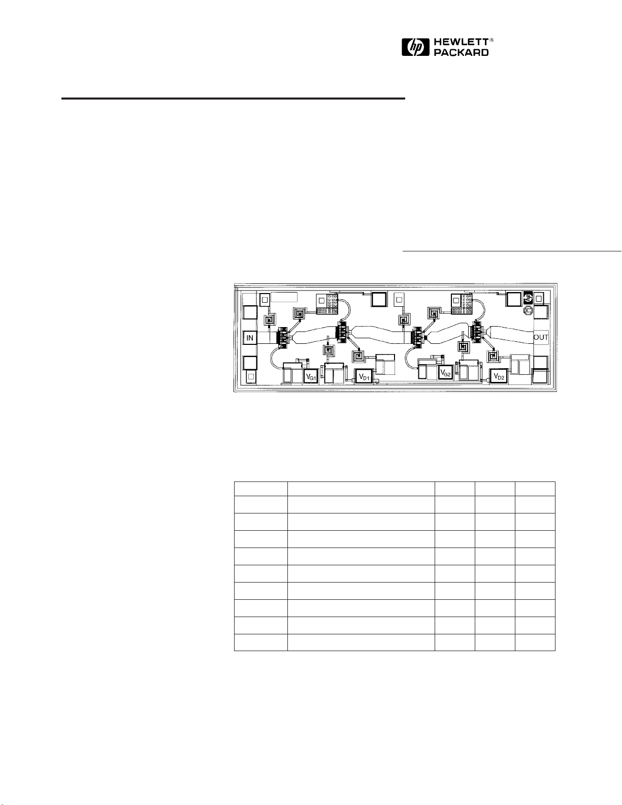
Biasing and Operation
The HMMC-5023 has four cascaded gain stages as shown in
Figure 1. The first two gain stages
at the input are biased with the
VD1 drain supply. Similarly the
two output stages are biased with
the VD2 supply. Standard LNA
operation is with a single positive
DC drain supply voltage
(VD1=VD2=5 V) using the assembly diagram shown in Figure 9(a).
If desired, the output stage DC
supply voltage (VD2) can be
increased to improve output
power capability while maintaining optimum low noise bias
conditions for the input section.
The output power may also be
adjusted by applying a positive
voltage at VG2 to alter the operating bias point for both output
FETs. Increasing the voltage
applied to VG2 (more positively)
results in a more negative gate-tosource voltage and, therefore,
lower drain current. Figures 9(b)
and 9(c) illustrate how the device
can be assembled for both
independent drain supply operation and for output-stage gate
bias control.
No ground wires are required
since ground connections are
made with plated through-holes
to the backside of the device.
Assembly Techniques
Solder die attach using a fluxless
gold-tin (AuSn) solder preform is
the recommended assembly
method. A conductive epoxy such
as ABLEBOND® 71-1LM1 or
ABLEBOND® 36-2 may also be
used for die attaching provided
the Absolute Maximum Thermal
Ratings are not exceeded. The
device should be attached to an
electrically conductive surface to
complete the DC and RF ground
paths. Ground path inductance
should be minimized (<10 pH) to
assure stable operation. The
backside metallization on the
device is gold.
It is recommended that the RF
input and RF output connections
be made using either 500 line/inch
(or equivalent) gold wire mesh, or
dual 0.7 mil diameter gold wire.
The RF wires should be kept as
short as possible to minimize
inductance. The bias supply wire
can be a 0.7 mil diameter gold
wire attached to either of the
VDD bonding pads.
Thermosonic wedge is the
preferred method for wire
bonding to the gold bond pads.
Mesh wires can be attached using
a 2 mil round tacking tool and a
tool force of approximately
22␣ grams with an ultrasonic
power of roughly 55 dB for a
duration of 76 ± 8 msec. A guided-
wedge at an ultrasonic power
level of 64 dB can be used for the
0.7 mil wire. The recommended
wire bond stage temperature is
150 ± 2 °C.
For more detailed information
see HP application note #999
“GaAs MMIC Assembly and
Handling Guidelines.”
GaAs MMICs are ESD sensitive.
Proper precautions should be used
when handling these devices.
INPUT STAGE OUTPUT STAGE
IN
92 Ω
V
G1
Figure 1. HMMC-5023 Simplified Schematic.
V
D1
92 Ω
6-36
OUT
V
G2
V
D2
Page 4

HMMC-5023 Typical Performance
V
= VD2 = 5.0 V
D1
30
Gain
26
22
18
14
SMALL-SIGNAL GAIN (dB)
10
19.0 20.2 21.4 22.6 23.8 25.0
Figure 2. Gain and Isolation vs.
Frequency.
Spec Range
21.2 – 23.6 GHz
FREQUENCY
Isolation
(GHz)
0
10
20
30
40
50
REVERSE ISOLATION (dB)
60
70
V
= VD2 = 5.0 V
D1
0
Spec Range
5
10
15
20
INPUT RETURN LOSS (dB)
25
19.0 20.2 21.4 22.6 23.8 25.0
Figure 3. Input and Output Return
Loss vs. Frequency.
21.2 – 23.6 GHz
Input
FREQUENCY
(GHz)
Output
0
5
10
15
20
OUTPUT RETURN LOSS (dB)
25
Typical Scattering Parameters
Freq. S
11
[1]
, (T
= 25° C, V
op
S
21
= VD2 = 5.0 V, VG1 = VG2 = Open, Z
D1
S
12
= 50 Ω
o
S
22
GHz dB Mag Ang dB Mag Ang dB Mag Ang dB Mag Ang
19.0 -6.3 0.486 61.9 -61.6 0.0008 122.7 22.3 13.090 83.3 -6.6 0.470 -179.1
19.2 -6.4 0.477 59.4 -61.6 0.0008 116.3 22.6 13.509 74.2 -6.9 0.450 175.7
19.4 -6.6 0.466 56.7 -61.0 0.0009 113.1 22.5 13.355 64.0 -7.4 0.427 169.7
19.6 -6.8 0.455 53.8 -61.3 0.0009 104.2 23.2 14.459 56.1 -7.9 0.403 163.5
19.8 -7.1 0.443 50.6 -62.3 0.0008 93.0 23.0 14.142 45.0 -8.4 0.381 156.5
20.0 -7.4 0.428 47.1 -61.2 0.0009 72.6 23.5 14.913 36.4 -8.9 0.358 148.8
20.2 -7.8 0.409 43.8 -61.3 0.0009 66.1 23.9 15.599 26.2 -9.5 0.333 139.9
20.4 -8.2 0.391 40.2 -60.9 0.0009 47.3 24.4 16.617 15.7 -10.2 0.309 130.7
20.6 -8.7 0.368 36.2 -59.5 0.0011 25.8 24.7 17.085 5.7 -10.8 0.290 119.5
20.8 -9.3 0.344 31.8 -59.6 0.0011 11.5 25.1 18.061 -4.7 -11.2 0.274 106.2
21.0 -10.0 0.318 27.4 -58.2 0.0012 -4.2 25.4 18.663 -15.3 -11.7 0.259 91.3
21.2 -10.8 0.288 22.9 -56.0 0.0016 -17.6 25.6 19.010 -26.6 -12.0 0.252 74.6
21.4 -11.8 0.256 18.4 -54.9 0.0018 -36.9 25.7 19.209 -38.7 -12.1 0.247 56.4
21.6 -13.1 0.220 14.9 -55.1 0.0018 -52.2 25.7 19.209 -51.3 -12.2 0.247 38.2
21.8 -14.7 0.185 12.1 -53.8 0.0020 -64.6 25.7 19.354 -61.4 -11.9 0.254 21.9
22.0 -16.5 0.149 11.0 -52.5 0.0024 -75.8 25.9 19.769 -74.0 -11.7 0.261 6.8
22.2 -18.5 0.118 12.1 -51.2 0.0028 -90.4 25.6 19.066 -85.2 -11.3 0.271 -6.6
22.4 -20.6 0.094 15.9 -50.5 0.0030 -100.3 25.6 19.113 -96.2 -11.0 0.282 -18.4
22.6 -22.7 0.074 22.8 -50.0 0.0031 -108.7 25.0 17.824 -107.5 -10.7 0.291 -28.7
22.8 -24.3 0.061 37.4 -49.3 0.0034 -118.9 25.1 17.943 -116.9 -10.5 0.298 -37.9
23.0 -24.9 0.057 54.0 -48.5 0.0037 -126.2 24.3 16.401 -127.6 -10.4 0.301 -45.5
23.2 -24.7 0.059 68.3 -47.6 0.0042 -134.9 24.2 16.279 -137.5 -10.4 0.300 -52.3
23.4 -24.2 0.061 78.9 -47.3 0.0043 -144.0 23.9 15.625 -146.3 -10.5 0.298 -58.0
23.6 -23.6 0.066 86.3 -47.2 0.0044 -148.9 23.2 14.469 -154.0 -10.6 0.295 -62.4
23.8 -23.3 0.068 93.5 -46.9 0.0045 -156.1 23.3 14.607 -163.4 -10.5 0.298 -65.9
24.0 -22.6 0.074 98.0 -46.4 0.0048 -161.1 22.4 13.168 -170.8 -10.6 0.296 -69.2
24.2 -22.2 0.078 100.8 -46.1 0.0049 -167.3 22.3 13.002 -179.0 -10.6 0.294 -72.0
24.4 -21.8 0.082 102.8 -45.5 0.0053 -171.7 21.6 12.087 173.1 -10.6 0.294 -74.7
24.6 -21.4 0.086 105.5 -45.6 0.0052 -176.4 21.8 12.350 166.3 -10.7 0.291 -76.8
24.8 -21.2 0.088 108.1 -44.9 0.0057 179.1 21.4 11.771 159.2 -10.8 0.289 -78.4
25.0 -20.9 0.091 293.2 -44.4 0.0061 353.0 21.0 11.257 331.9 -10.8 0.289 -79.3
Note:
1. Data obtained from wafer-probed measurements.
6-37
Page 5

HMMC-5023 Typical Performance
V
= VD2 = 5.0 V
D1
30
26
22
18
14
SMALL-SIGNAL GAIN (dB)
Spec Range
21.2 – 23.6 GHz
0.02 dB/°C
typical
[1]
–55°C
–30°C
0° C
+30°C
+60°C
+100°C
V
= VD2 = 5.0 V, TA = 25°C
D1
5
4
3
2
NOISE FIGURE (dB)
1
Spec Range
21.2 – 23.6 GHz
[3]
10
19.0 20.2 21.4 22.6 23.8 25.0
FREQUENCY
(GHz)
Figure 4. Small-Signal Gain vs.
Frequency and Ambient Temperature
V
= VD2 = 5.0 V
D1
20
21 GHz
25
Gain
20
GAIN (dB)
15
10
24681012
Figure 6. Gain Compression and
Efficiency Characteristics
23 GHz
OUTPUT POWER (dBm)
[2]
η
added
.
[1]
.
20
15
10
5
POWER-ADDED EFFICIENCY (%)
0
0
19.0 20.2 21.4 22.6 23.8 25.0
FREQUENCY
(GHz)
Figure 5. Noise Figure vs. Frequency
V
= VD2 = 5.0 V, fO = 22 GHz
D1
0
–15
–30
–45
2nd Harmonic
SMALL HARMONIC DISTORTION (dBc)
–60
24681012
OUTPUT POWER (dBm)
Figure 7. Second Harmonic and Gain
Compression Characteristics
Gain
[2]
.
30
25
20
15
10
Notes:
1. Device tested while mounted on a HP83040 Modular Microcircuit Fixture calibrated at the coaxial
connectors. Test results shown have been degraded by the fixture due to loss and impedance mismatch
errors. The temperature coefficient of the fixture alone is approximately 0.003 dB/°C at 20 GHz.
2. Data obtained from wafer-probed measurements.
3. The temperature coefficient of noise figure was measured for one device mounted on a HP83040 Modular
Microcircuit Fixture. The uncorrected result, <0.014 dB/°C, includes the effects of the fixture.
[2]
.
GAIN (dB)
600
520
RF INPUT
300
80
0
0 435 755 1235 1555 1880
Figure 8. HMMC-5023 Bonding Pad Locations. (Dimensions are in micrometers)
6-38
RF OUTPUT
300
105 (VG2 Y-axis)
0
Page 6

Gold Plated Shim (Optional)
RF
RF
IN
IN
V
D1
V
D2
RF
OUT
V
G2
RF
OUT
≥20 pF Capacitor
≥20 pF Capacitor
To V
DC Power Supply
DD
V
D1
R
R
V
D2
R (typ.) ≥90 Ω
Figure 9a. Single DC Drain Supply. Figure 9b. Assembly for custom biasing of output gain
stages using an external chip resistor.
To V
(Optional)
RF
IN
G2
≥20 pF Capacitor
RF
IN
V
G2
V
RF
OUT
V
V
D1
D2
V
D1
G2
RF
OUT
V
D2
DC Power Supply
≥20 pF Capacitor
To V
DC Power Supply
D1
To VD2
DC Power Supply
Figure 9c. A VG2 DC supply or a resistive divider network can also be used to bias the output stages for custom applications.
Figure 9. HMMC-5023 Assembly Diagram Examples.
This data sheet contains a variety of typical and guaranteed performance data. The
information supplied should not be interpreted as a complete list of circuit specifications. In this data sheet the term typical refers to the 50th percentile performance. For
additional information contact your local HP sales representative.
6-39
 Loading...