

Page 1
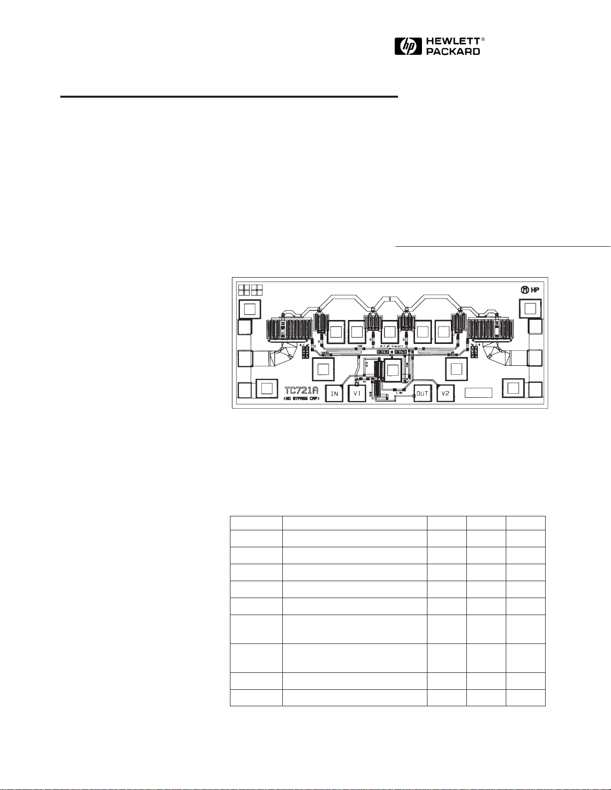
DC – 50 GHz Variable Attenuator
Technical Data
Features
• Specified Frequency Range:
DC - 26.5 GHz
• Return Loss: 10 dB
• Minimum Attenuation:
2.0␣ dB
• Maximum Attenuation:
30.0␣ dB
HMMC-1002
Description
The HMMC-1002 is a monolithic,
voltage variable, GaAs IC attenuator that operates from DC to
50␣ GHz. It is fabricated using
MWTC’s MMICB process which
features an MBE epitaxial layer,
backside ground vias, and FET
gate lengths of approximately
0.4␣ mm. The variable resistive
elements of the HMMC-1002 are
two 750 mm wide series FETs
and four 200 mm wide shunt
FETs. The distributed topology of
the HMMC-1002 minimizes the
parasitic effects of its series and
shunt FETs, allowing the
HMMC-1002 to exhibit a wide
dynamic range across its full
bandwidth. An on-chip DC
reference circuit may be used to
maintain optimum VSWR for any
attenuation setting or to improve
the attenuation versus voltage
linearity of the attenuator circuit.
Chip Size: 1470 x 610 µm (57.9 x 24.0 mils)
Chip Size Tolerance: ± 10 µm (± 0.4 mils)
Chip Thickness: 127 ± 15 µm (5.0 ± 0.6 mils)
RF Pad Dimensions: 60 x 70 µm (2.4 x 2.8 mils), or larger
DC Pad Dimensions: 75 x 75 µm (3.0 x 3.0 mils), or larger
Absolute Maximum Ratings
[1]
Symbol Parameters/Conditions Units Min. Max.
V
DC-RF
V
1
V
2
V
DC
P
in
T
mina
T
maxa
T
STG
T
max
Note:
1. Operation in excess of any one of these conditions may result in permanent
damage to this device.
DC Voltage to RF Ports V -0.6 +1.6
V1 Control Voltage V -5.0 +0.5
V1 Control Voltage V -5.0 +0.5
DC In/DC Out V -0.6 +1.0
RF Input Power dBm 17
Minimum Ambient
Operating Temperature
Maximum Ambient
Operating Temperature
°C -55
°C +125
Storage Temperature °C -6 5 +165
Maximum Assembly Temp. °C +300
5965-5452E
7-12
Page 2
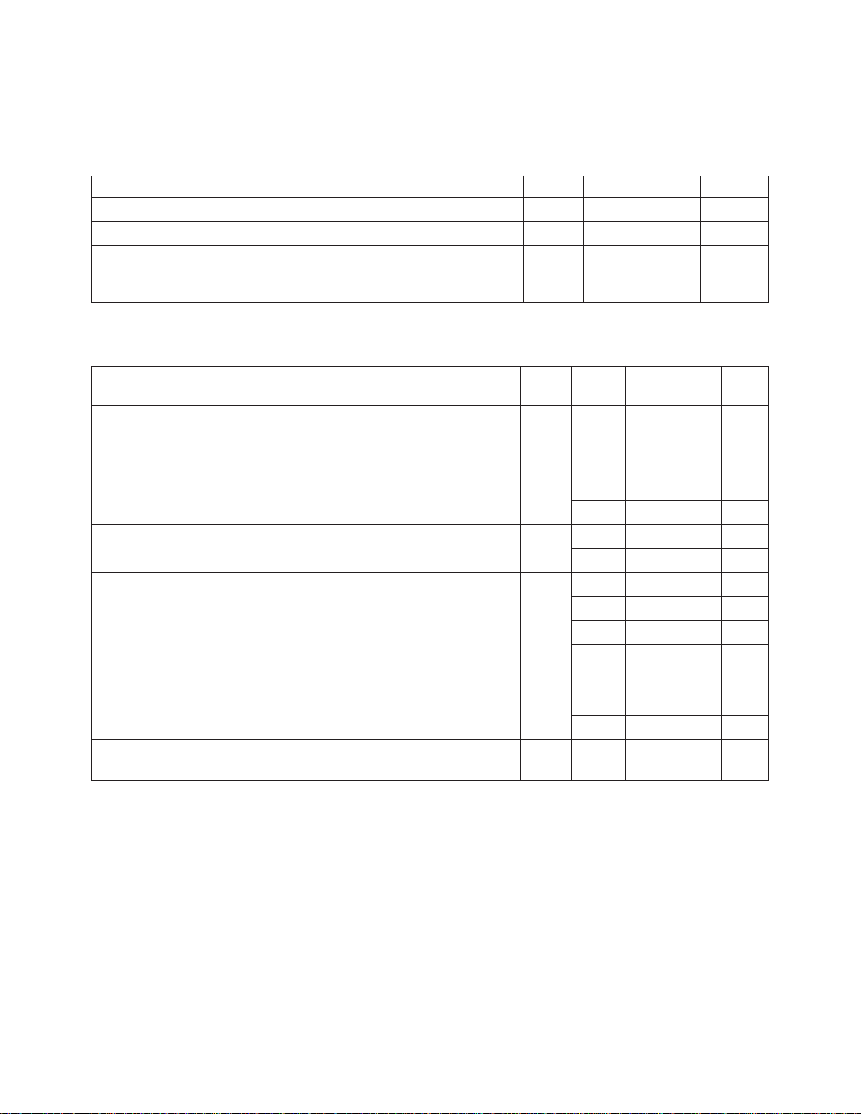
DC Specifications/Physical Properties, T
= 25°C
A
Symbol Parameters and Test Conditions Units Min. Typ. Max.
I
V1
I
V2
V1 Control Current, (V1 = -4V) mA 5.3 9.3 12
V2 Control Current, (V2 = -4V) mA 5.3 9.3 12
Pinch-off Voltage (V2, with V1 = 0 V)
V
p
Four 200 µm wide shunt FETs, V
= 1 V @ RFin, V -0.6 -1.3 -2.5
DD
IDD = 5 mA
Electrical Specifications
[1]
, T
= 25°C, ZO = 50 Ω
A
Parameters and Test Conditions Units
Minimum Attenuation, |S21|V
= 0 V, V2 = -4 V d B 20.00 1.7 2.4
1
Input/Output Return Loss @ Min. Attenuation Setting,
V1 = 0 V, V2 = - 4 V <50.0 8
dB
Freq.
(GHz)
Min. Typ. Max.
1.5 1.0 2.4
8.0 1.4 2.4
26.5 2.0 2.4
50.0 3.9
<26.5 10 16
1. 5 27 30
8. 0 27 38
Maximum Attenuation, |S21|V
= -4 V, V2 = 0 V d B 20.0 27 38
1
Input/Output Return Loss @ Max. Attenuation Setting,
V1 = -4 V, V2 = 0 V <50.0 10
DC Power Dissipation
(does not include input signals) V1 = -5 V, V2 = -5 V
mW 152
dB
26.5 27 40
50.0 35
<26.5 8 10
7-13
Page 3
Applications
The HMMC-1002 is designed to be
used as a gain control block
in an AGC assembly. Because of
its wide dynamic range and
return loss performance, the
HMMC-1002 may also be used as
a broadband pulse modulator or
single-pole single-throw, nonreflective switch.
Operation
The attenuation of the
HMMC-1002 is adjusted by
applying negative voltages to V1
and V2. V1 controls the drain-tosource resistances of the series
FETs while V2 controls the drainto-source resistances of the shunt
FETs. For any HMMC-1002 the
values of V1 may be adjusted so
that the device attenuation versus
voltage is monotonic for both V1
and V2; however, this will slightly
degrade the input and output
return loss.
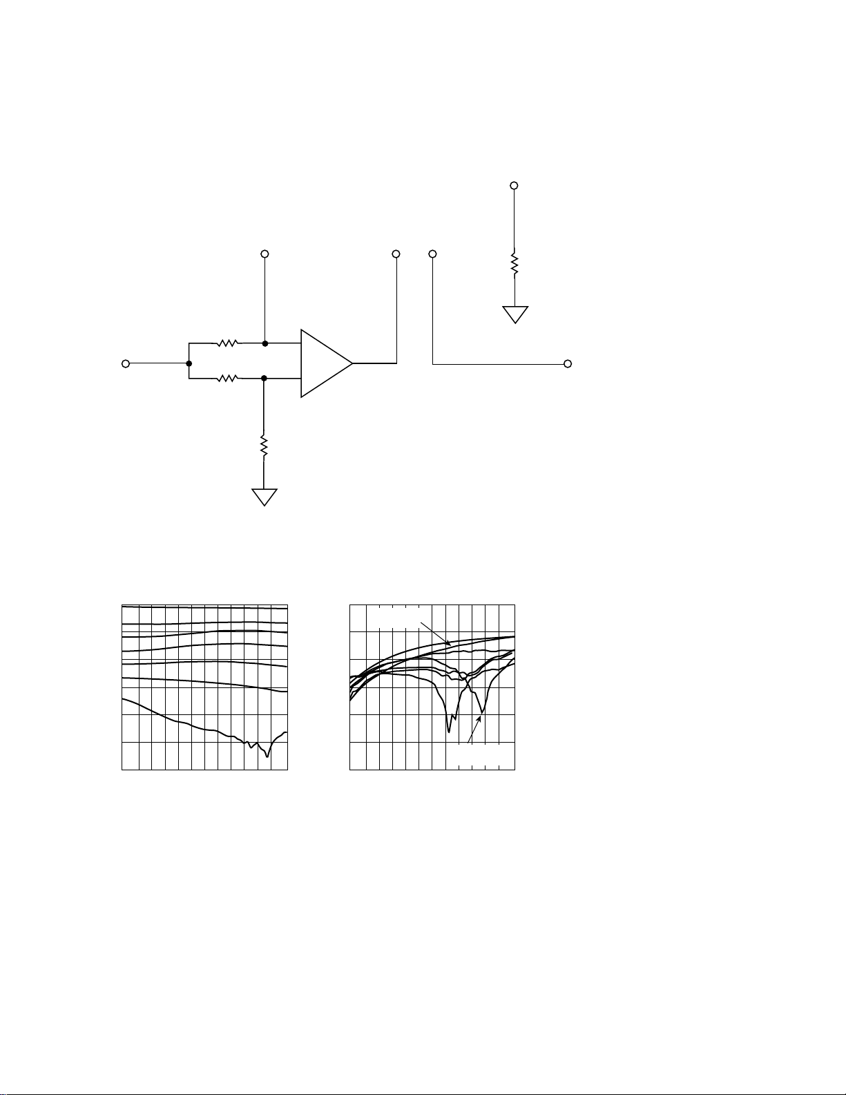
The attenuation of the
HMMC-1002 may also be controlled using only a single input
voltage by utilizing the on-chip
DC reference circuit and the
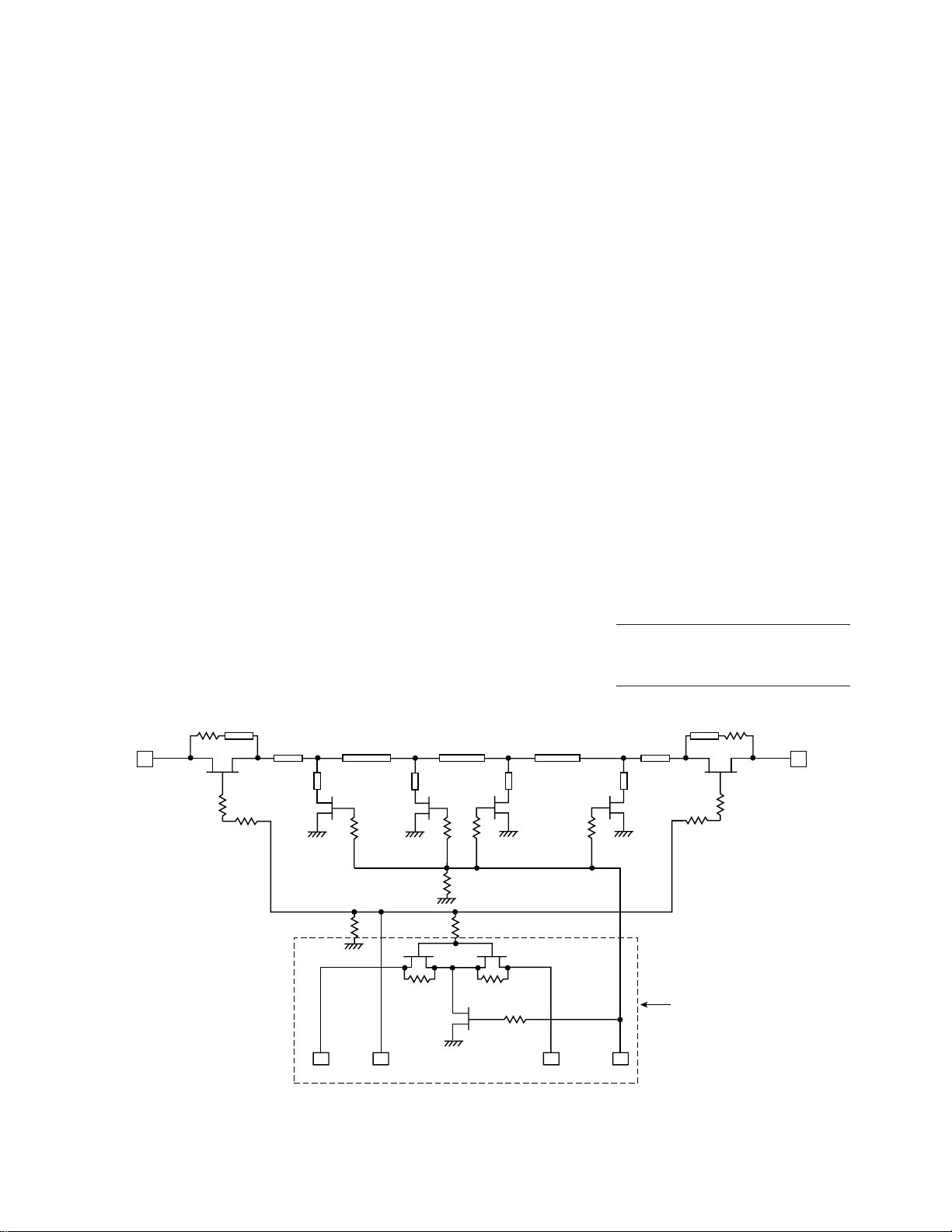
driver circuit shown in Figure 4.
This circuit optimizes VSWR for
any attenuation setting. Because
of process variations, the values
of V
REF
, R
, and RL are different
REF
for each wafer if optimum
performance is required. Typical
values for these elements are
given. The ratio of the resistors
R1 and R2 determines the sensitivity of the attenuation versus
voltage performance of the
attenuator. For more information
on the performance of the
HMMC-1002 and the driver
circuits previously mentioned see
MWTC’s Application Note #37,
“HMMC-1002 Attenuator: Attenuation Control.” For more
S-parameter information, see
MWTC’s Application Note #44,
“HMMC-1002 Attenuator:
S-Parameters.”
Assembly Techniques
Solder die attach using a AuSn
solder preform is the recommended assembly method;
however, an epoxy die attach
method using ABLEBOND
71-1LM1 or ABLEBOND® 36-2
may also be employed. Gold
thermosonic wedge bonding with
0.7 mil wire is the recommended
method for bonding to the device.
Tool force should be
22␣ grams␣ ± ␣ 1␣ gram, stage temperature is 150␣ ± ␣2°C, and ultrasonic
power and duration of 64 ± 1␣ dB
and 76 ± 8␣ msec, respectively.
The top and bottom metallization
is gold.
For more detailed information
see HP application note #999
“GaAs MMIC Assembly and
Handling Guidelines.”
GaAs MMICs are ESD sensitive.
Proper precautions should be used
when handling these devices.
®
RF
IN
Figure 1. HMMC-1002 Schematic.
DC
RF
OUT
DC Reference Circuit
IN
V
1
DC
OUT
V
2
7-14
Page 4
610
233
RF
IN
0
584
0
476
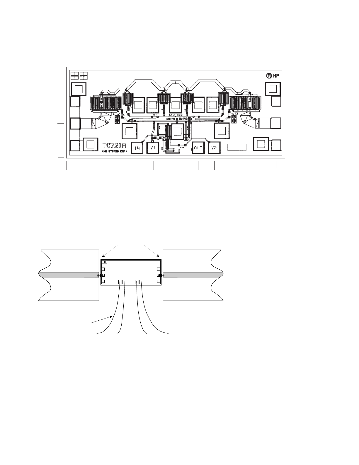
Notes:
1. All dimensions in microns and shown to center of bond pad.
2. DCin, V1, DC
, and V2 bonding pads are 75 x 75 microns.
out
3. RF input and output bonding pads are 60 x 70 microns.
4. Chip thickness: 127 ± 15 µm.
Figure 2. HMMC-1002 Bonding Pad Locations.
2.0 mil
nom. gap
RF
IN
TC721A
887 994
RF
OUT
RF
OUT
1410
233
1470
4 Wire Bonds using
0.7 mil dia. Gold Bond Wire
(Length NOT important)
DC
V
IN
1
Figure 3. HMMC-1002 Assembly Diagram.
DC
OUT
V
2
7-15
Page 5
DC
To
OUT
To
DC
IN
–
+
R
REF
Op. Amp
V
REF
(-0.4V to -1.0V)
500 Ω
500 Ω
(350 Ω – 500 Ω)
Figure 4. Attenuator Driver.
HMMC-1002 Typical Performance
0
10
0
10
To
V
1
Maximum
Attenuation
To
V
2
R
L
(400 Ω – 500 Ω)
V
IN
(0V to -4.0V)
20
30
40
INSERTION LOSS (dB)
50
60
1.5 4.0 8.0 12.0 16.0 24.020.0 26.5
FREQUENCY (GHz)
Figure 5. Attenuation vs. Frequency
[1]
20
30
40
RETURN LOSS (dB)
50
60
1.5 4.0 8.0 12.0 16.0 24.020.0 26.5
.
Figure 6. Output Return Loss vs.
Frequency
Note:
1. Data obtained from on-wafer measurements. T
FREQUENCY (GHz)
[1]
= 25°C.
chuck
.
7-16
Minimum
Attenuation
Page 6
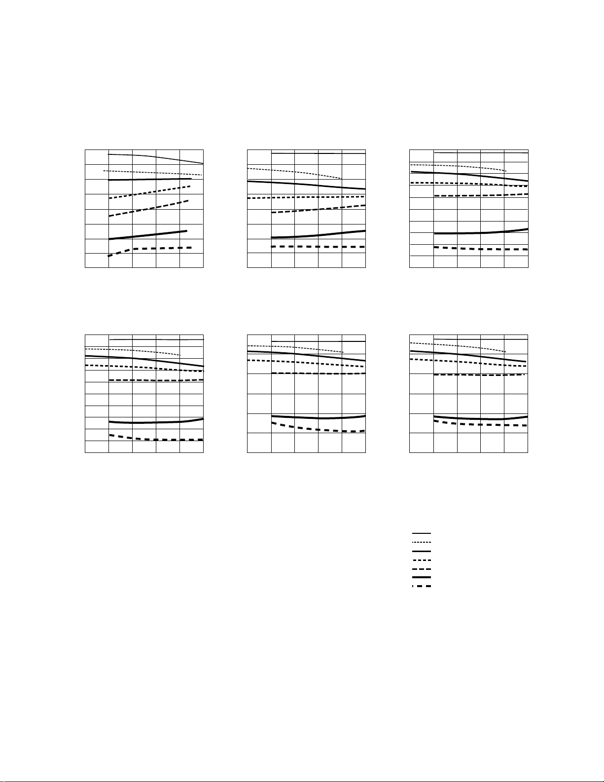
HMMC-1002 Typical Power Performance
All Attenuation Settings were done at 1 GHz.
0
10
20
ATTENUATION (dB)
30
40
-5 5 10 15020
INPUT POWER (dBm)
Figure 7. Attenuation vs. Input Power
@ 50.0 MHz.
0
10
20
30
ATTENUATION (dB)
40
[1]
.
0
10
20
ATTENUATION (dB)
30
40
-5 5 10 15020
Figure 8. Attenuation vs. Input Power
@ 2.0 GHz.
0
10
20
30
40
ATTENUATION (dB)
50
INPUT POWER (dBm)
[1]
.
0
10
20
30
ATTENUATION (dB)
40
50
-5 5 10 15020
INPUT POWER (dBm)
Figure 9. Attenuation vs. Input Power
@ 10.0 GHz.
0
10
20
30
40
ATTENUATION (dB)
50
[1]
.
50
-5 5 10 15020
INPUT POWER (dBm)
Figure 10. Attenuation vs. Input Power
@ 14.0 GHz.
[1]
.
60
-5 5 10 15020
INPUT POWER (dBm)
Figure 11. Attenuation vs. Input Power
@ 18.0 GHz.
[1]
.
Note:
1. Data taken with the device mounted in connectorized package.
60
-5 5 10 15020
INPUT POWER (dBm)
Figure 12. Attenuation vs. Input Power
@ 22.0 GHz.
[1]
.
Key for Attenuation Settings:
Min.
Min. + 5 dB
Min. + 10 dB
Min. + 15 dB
Min. + 20 dB
Min. + 30 dB
Max.
7-17
Page 7
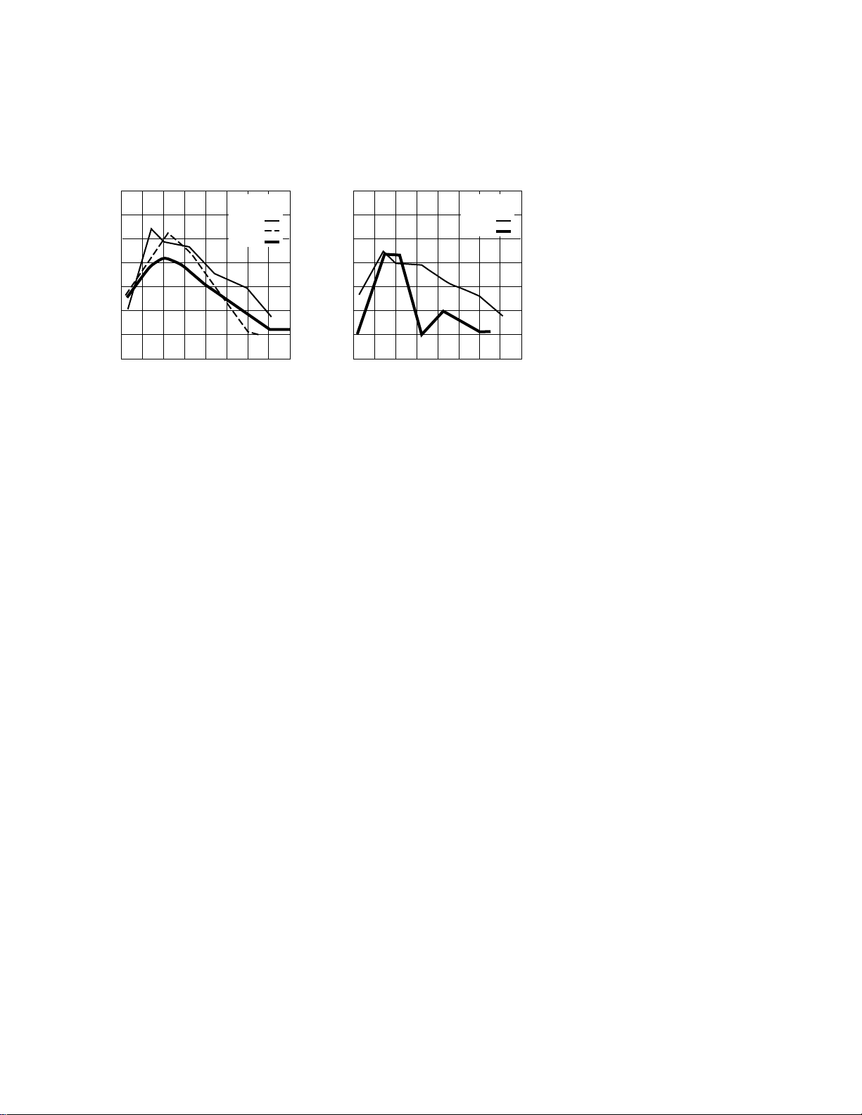
HMMC-1002 Typical Harmonic Performance
-20
-30
-40
-50
-60
-70
HARMONICS (dBc)
-80
-90
0 5 10 15 20 3025 4035
ATTENUATION (dB)
Fundamental
Frequency:
50 MHz
10 GHz
2 GHz
Figure 13. Second Harmonic
Suppression vs. Attenuation. Input
Power = 0 dBm
[1]
.
-20
-30
-40
-50
-60
-70
HARMONICS (dBc)
-80
-90
0 5 10 15 20 3025 4035
ATTENUATION (dB)
Figure 14. Third Harmonic
Suppression vs. Attenuation. Input
Power = 0 dBm
[1]
.
Note:
1. Data taken with the device mounted in connectorized package.
Fundamental
Frequency:
50 MHz
2 GHz
7-18
Page 8
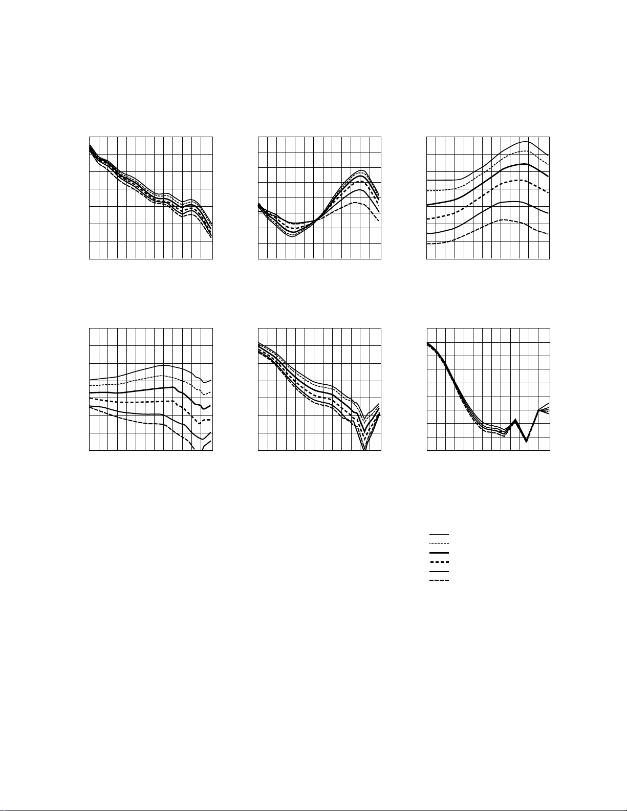
HMMC-1002 Typical Temperature Performance
1.5
1
3.5
(dB)
21
2
(dB)
21
5.5
(dB)
21
12
8
3
ATTENUATION S
4
2 101418226 26.5
FREQUENCY (GHz)
Figure 15. Attenuation vs. Temperature
@ Minimum Attenuation.
18
(dB)
21
22
26
ATTENUATION S
30
2 101418226 26.5
FREQUENCY (GHz)
Figure 18. Attenuation vs. Temperature
@ 20 dB Attenuation.
[2]
.
[2]
.
7.5
ATTENUATION S
9.5
2 101418226 26.5
FREQUENCY (GHz)
Figure 16. Attenuation vs. Temperature
@ 5 dB Attenuation.
28
(dB)
21
32
36
ATTENUATION S
40
2 101418226 26.5
FREQUENCY (GHz)
Figure 19. Attenuation vs. Temperature
@ 30 dB Attenuation.
[2]
.
[2]
.
16
ATTENUATION S
20
2 101418226 26.5
FREQUENCY (GHz)
Figure 17. Attenuation vs. Temperature
@ 10 dB Attenuation.
32
(dB)
36
21
40
44
ATTENUATION S
48
2 101418226
FREQUENCY (GHz)
Figure 20. Attenuation vs. Temperature
@ Max. Attenuation.
[2]
.
26.5
[2]
.
Note:
1. Data taken with the device mounted in connectorized package.
This data sheet contains a variety of typical and guaranteed performance data. The
information supplied should not be interpreted as a complete list of circuit specifications. In this data sheet the term typical refers to the 50th percentile performance. For
additional information contact your local HP sales representative.
7-19
Key for Temperature Settings:
-55°C
-25°C
0° C
+25°C
+55°C
+85°C
 Loading...