HP HMMC-2006 Datasheet

DC – 6 GHz Unterminated SPDT
Switch
Technical Data
Features
• Frequency Range: DC-6 GHz
• Insertion Loss:
<1dB @ 6 GHz
• Isolation:
>70 dB @ 45 MHz
>35 dB @ 6 GHz
• Return Loss: >12 dB
(Both Input & Output)
• Switching Speed: <1 ns
•P
-1dB
:
23 dBm @ 50 MHz
>27dBm @ 6 GHz
• Harmonics: <-25 dBc @
20␣ dBm (DC coupled)
Description
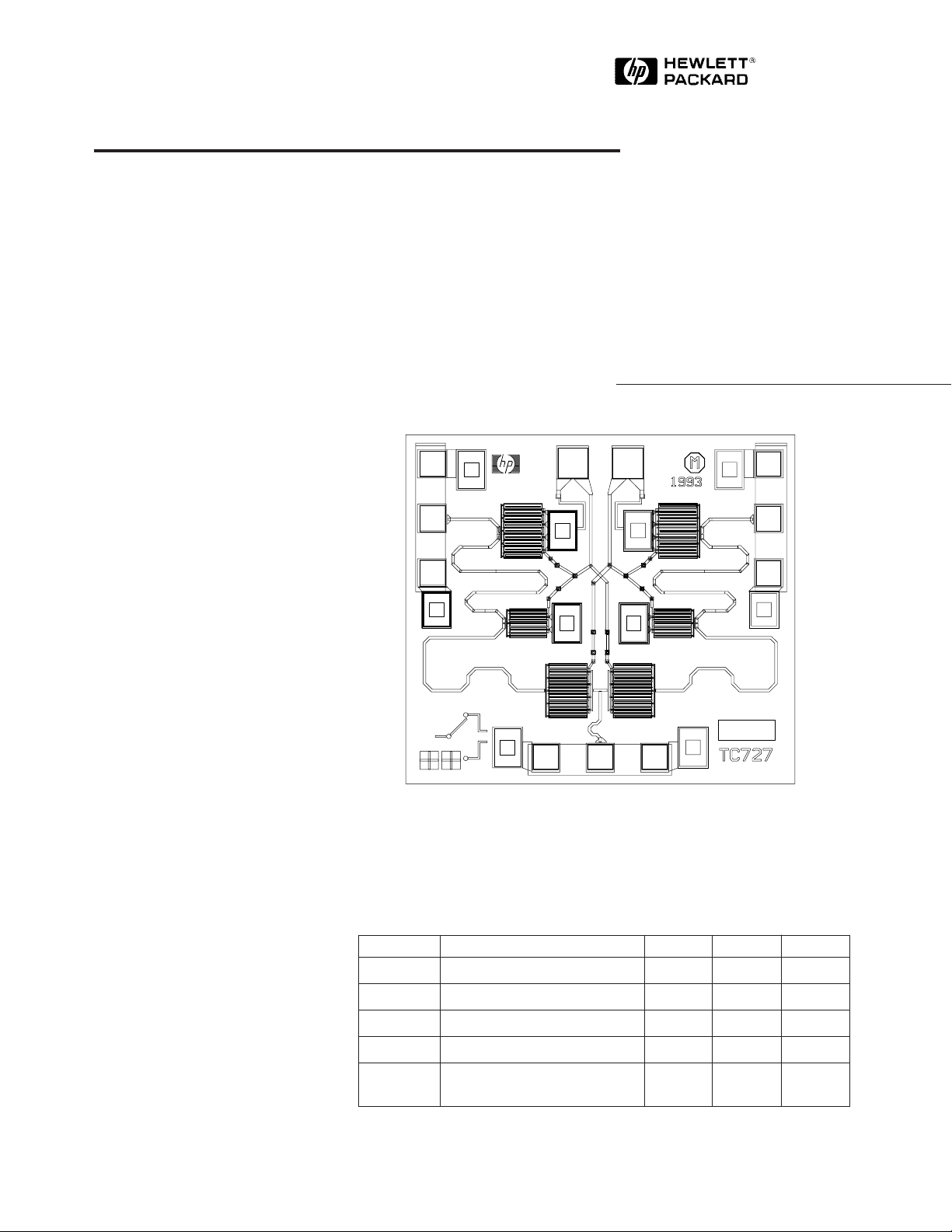
The HMMC-2006 is a GaAs
monolithic microwave integrated
circuit (MMIC) designed for low
insertion loss and high isolation
from DC to 6 GHz. It is intended
for use as a general-purpose,
singlepole, double-throw (SPDT)
switch. One series and two shunt
MESFETs per throw provide
1.2␣ dB maximum insertion loss
and 35 dB minimum isolation at
6␣ GHz. HMMC-2006 chips use
through-substrate vias to provide
ground connections to the chip
backside and minimize the
number of wire bonds required.
The HMMC-2006 is also available
in an 8-lead flatpack (1GG7-4201).
Chip Size: 960 x 1070 µm (37.8 x 42.1 mils)
Chip Size Tolerance: +0, -10 µm (+0, -0.4 mils)
Chip Thickness: 127 ± 15 µm (5.0 ± 0.6 mils)
Pad Dimensions: 80 x 80 µm (3.2 x 3.2 mils), or larger
Absolute Maximum Ratings
Symbol Parameters/Conditions Units Min. Max.
Note:
1. Operation in excess of any one of these conditions may result in permanent
damage to this device. T
RF
OUT2
V
sel
P
in
T
op
T
STG
T
max
Select Voltages 1 and 2 V -12 +3
RF Input Power dBm 30
Operating Temperature °C -5 5 +125
Storage Temperature °C -6 5 +165
Maximum Assembly Temp.
(for 60 seconds max.)
= 25° C except for T
A
HMMC-2006
SEL1 SEL2
RF
IN
[1]
RF
OUT1
Chip ID
°C +300
, T
, and T
ch
STG
max
.
5965-9071E
7-20

DC Specifications/Physical Properties, T
= 25°C
A
Symbol Parameters and Test Conditions Units Min. Typ. Max.
I
l
V
p
BV
gss
RF Specifications, T
Leakage Current @ -10 V µA 100
Pinch-off Voltage @ 8 mA V -6.75 -3.25
Breakdown Voltage Total V -18.0 -12.5
= 25°C, ZO = 50 Ω, V
A
high = 0 V, V
sel
low = -10 V
sel
Symbol Parameters and Test Conditions Units Min. Typ. Max.
BW Guaranteed Operating Bandwidth GHz DC 6
IL Insertion Loss, RFin to RF
ISO Isolation, RFin to RF
RL
RL
P
out
1 dB
t
s
in
Input Return Loss dB 12 14
Output Return Loss dB 12 15
Input Power where IL increases by 1 dB f = 50 MHz dBm 18 23
Switching Speed, 10% – 90% RF Envelope, f = 2 GHz ns 1
out
, f = 6 GHz, ON throw dB 1 1.2
out
, f = 6 GHz, OFF throw dB 35 40
7-21
 Loading...